WO2023210475A1 - 光学フィルタ - Google Patents
光学フィルタ Download PDFInfo
- Publication number
- WO2023210475A1 WO2023210475A1 PCT/JP2023/015700 JP2023015700W WO2023210475A1 WO 2023210475 A1 WO2023210475 A1 WO 2023210475A1 JP 2023015700 W JP2023015700 W JP 2023015700W WO 2023210475 A1 WO2023210475 A1 WO 2023210475A1
- Authority
- WO
- WIPO (PCT)
- Prior art keywords
- optical filter
- wavelength
- transmittance
- absorber
- filter according
- Prior art date
Links
- 230000003287 optical effect Effects 0.000 title claims abstract description 127
- 238000010521 absorption reaction Methods 0.000 claims abstract description 70
- 229910052769 Ytterbium Inorganic materials 0.000 claims abstract description 38
- 239000006096 absorbing agent Substances 0.000 claims abstract description 37
- NAWDYIZEMPQZHO-UHFFFAOYSA-N ytterbium Chemical compound [Yb] NAWDYIZEMPQZHO-UHFFFAOYSA-N 0.000 claims abstract description 34
- 239000011347 resin Substances 0.000 claims abstract description 29
- 229920005989 resin Polymers 0.000 claims abstract description 29
- 229910010272 inorganic material Inorganic materials 0.000 claims abstract description 18
- 239000011147 inorganic material Substances 0.000 claims abstract description 18
- 238000002834 transmittance Methods 0.000 claims description 108
- 230000003595 spectral effect Effects 0.000 claims description 103
- 239000011521 glass Substances 0.000 claims description 64
- 238000003384 imaging method Methods 0.000 claims description 12
- 239000000463 material Substances 0.000 claims description 11
- 239000000203 mixture Substances 0.000 claims description 8
- 239000013078 crystal Substances 0.000 claims description 7
- FIXNOXLJNSSSLJ-UHFFFAOYSA-N ytterbium(III) oxide Inorganic materials O=[Yb]O[Yb]=O FIXNOXLJNSSSLJ-UHFFFAOYSA-N 0.000 claims 1
- 239000000975 dye Substances 0.000 description 95
- 239000010410 layer Substances 0.000 description 80
- 238000010586 diagram Methods 0.000 description 16
- 150000001875 compounds Chemical class 0.000 description 15
- 239000000919 ceramic Substances 0.000 description 11
- JNDMLEXHDPKVFC-UHFFFAOYSA-N aluminum;oxygen(2-);yttrium(3+) Chemical compound [O-2].[O-2].[O-2].[Al+3].[Y+3] JNDMLEXHDPKVFC-UHFFFAOYSA-N 0.000 description 9
- 238000000576 coating method Methods 0.000 description 9
- 229910019901 yttrium aluminum garnet Inorganic materials 0.000 description 9
- 229910004298 SiO 2 Inorganic materials 0.000 description 8
- 230000002745 absorbent Effects 0.000 description 8
- 239000002250 absorbent Substances 0.000 description 8
- 239000003513 alkali Substances 0.000 description 8
- 239000011248 coating agent Substances 0.000 description 8
- 238000000034 method Methods 0.000 description 7
- YMWUJEATGCHHMB-UHFFFAOYSA-N Dichloromethane Chemical compound ClCCl YMWUJEATGCHHMB-UHFFFAOYSA-N 0.000 description 6
- 229910010413 TiO 2 Inorganic materials 0.000 description 6
- 230000031700 light absorption Effects 0.000 description 6
- 239000002585 base Substances 0.000 description 5
- VZSRBBMJRBPUNF-UHFFFAOYSA-N 2-(2,3-dihydro-1H-inden-2-ylamino)-N-[3-oxo-3-(2,4,6,7-tetrahydrotriazolo[4,5-c]pyridin-5-yl)propyl]pyrimidine-5-carboxamide Chemical compound C1C(CC2=CC=CC=C12)NC1=NC=C(C=N1)C(=O)NCCC(N1CC2=C(CC1)NN=N2)=O VZSRBBMJRBPUNF-UHFFFAOYSA-N 0.000 description 4
- 239000011358 absorbing material Substances 0.000 description 4
- 230000005540 biological transmission Effects 0.000 description 4
- 230000000903 blocking effect Effects 0.000 description 4
- 239000010419 fine particle Substances 0.000 description 4
- 229920001721 polyimide Polymers 0.000 description 4
- 239000009719 polyimide resin Substances 0.000 description 4
- 239000002904 solvent Substances 0.000 description 4
- ANRHNWWPFJCPAZ-UHFFFAOYSA-M thionine Chemical compound [Cl-].C1=CC(N)=CC2=[S+]C3=CC(N)=CC=C3N=C21 ANRHNWWPFJCPAZ-UHFFFAOYSA-M 0.000 description 4
- 238000007740 vapor deposition Methods 0.000 description 4
- DEXFNLNNUZKHNO-UHFFFAOYSA-N 6-[3-[4-[2-(2,3-dihydro-1H-inden-2-ylamino)pyrimidin-5-yl]piperidin-1-yl]-3-oxopropyl]-3H-1,3-benzoxazol-2-one Chemical compound C1C(CC2=CC=CC=C12)NC1=NC=C(C=N1)C1CCN(CC1)C(CCC1=CC2=C(NC(O2)=O)C=C1)=O DEXFNLNNUZKHNO-UHFFFAOYSA-N 0.000 description 3
- AFCARXCZXQIEQB-UHFFFAOYSA-N N-[3-oxo-3-(2,4,6,7-tetrahydrotriazolo[4,5-c]pyridin-5-yl)propyl]-2-[[3-(trifluoromethoxy)phenyl]methylamino]pyrimidine-5-carboxamide Chemical compound O=C(CCNC(=O)C=1C=NC(=NC=1)NCC1=CC(=CC=C1)OC(F)(F)F)N1CC2=C(CC1)NN=N2 AFCARXCZXQIEQB-UHFFFAOYSA-N 0.000 description 3
- 230000007423 decrease Effects 0.000 description 3
- 150000002500 ions Chemical class 0.000 description 3
- 239000007788 liquid Substances 0.000 description 3
- 239000001007 phthalocyanine dye Substances 0.000 description 3
- -1 polyparaphenylene Polymers 0.000 description 3
- 229910001415 sodium ion Inorganic materials 0.000 description 3
- WNZQDUSMALZDQF-UHFFFAOYSA-N 2-benzofuran-1(3H)-one Chemical compound C1=CC=C2C(=O)OCC2=C1 WNZQDUSMALZDQF-UHFFFAOYSA-N 0.000 description 2
- YLZOPXRUQYQQID-UHFFFAOYSA-N 3-(2,4,6,7-tetrahydrotriazolo[4,5-c]pyridin-5-yl)-1-[4-[2-[[3-(trifluoromethoxy)phenyl]methylamino]pyrimidin-5-yl]piperazin-1-yl]propan-1-one Chemical compound N1N=NC=2CN(CCC=21)CCC(=O)N1CCN(CC1)C=1C=NC(=NC=1)NCC1=CC(=CC=C1)OC(F)(F)F YLZOPXRUQYQQID-UHFFFAOYSA-N 0.000 description 2
- 229920000178 Acrylic resin Polymers 0.000 description 2
- 239000004925 Acrylic resin Substances 0.000 description 2
- RTZKZFJDLAIYFH-UHFFFAOYSA-N Diethyl ether Chemical compound CCOCC RTZKZFJDLAIYFH-UHFFFAOYSA-N 0.000 description 2
- 229910021193 La 2 O 3 Inorganic materials 0.000 description 2
- FHKPLLOSJHHKNU-INIZCTEOSA-N [(3S)-3-[8-(1-ethyl-5-methylpyrazol-4-yl)-9-methylpurin-6-yl]oxypyrrolidin-1-yl]-(oxan-4-yl)methanone Chemical compound C(C)N1N=CC(=C1C)C=1N(C2=NC=NC(=C2N=1)O[C@@H]1CN(CC1)C(=O)C1CCOCC1)C FHKPLLOSJHHKNU-INIZCTEOSA-N 0.000 description 2
- MWPLVEDNUUSJAV-UHFFFAOYSA-N anthracene Chemical compound C1=CC=CC2=CC3=CC=CC=C3C=C21 MWPLVEDNUUSJAV-UHFFFAOYSA-N 0.000 description 2
- 229910052792 caesium Inorganic materials 0.000 description 2
- TVFDJXOCXUVLDH-UHFFFAOYSA-N caesium atom Chemical compound [Cs] TVFDJXOCXUVLDH-UHFFFAOYSA-N 0.000 description 2
- 230000008859 change Effects 0.000 description 2
- 229940125904 compound 1 Drugs 0.000 description 2
- 229940125782 compound 2 Drugs 0.000 description 2
- 229940126214 compound 3 Drugs 0.000 description 2
- 229940125898 compound 5 Drugs 0.000 description 2
- 238000001035 drying Methods 0.000 description 2
- 238000010030 laminating Methods 0.000 description 2
- 229910001416 lithium ion Inorganic materials 0.000 description 2
- DZVCFNFOPIZQKX-LTHRDKTGSA-M merocyanine Chemical compound [Na+].O=C1N(CCCC)C(=O)N(CCCC)C(=O)C1=C\C=C\C=C/1N(CCCS([O-])(=O)=O)C2=CC=CC=C2O\1 DZVCFNFOPIZQKX-LTHRDKTGSA-M 0.000 description 2
- 229920005668 polycarbonate resin Polymers 0.000 description 2
- 239000004431 polycarbonate resin Substances 0.000 description 2
- 229920001225 polyester resin Polymers 0.000 description 2
- 239000004645 polyester resin Substances 0.000 description 2
- 229920005672 polyolefin resin Polymers 0.000 description 2
- 230000008569 process Effects 0.000 description 2
- 239000002994 raw material Substances 0.000 description 2
- 238000001228 spectrum Methods 0.000 description 2
- 238000004528 spin coating Methods 0.000 description 2
- PBYZMCDFOULPGH-UHFFFAOYSA-N tungstate Chemical compound [O-][W]([O-])(=O)=O PBYZMCDFOULPGH-UHFFFAOYSA-N 0.000 description 2
- 238000000870 ultraviolet spectroscopy Methods 0.000 description 2
- BCHZICNRHXRCHY-UHFFFAOYSA-N 2h-oxazine Chemical compound N1OC=CC=C1 BCHZICNRHXRCHY-UHFFFAOYSA-N 0.000 description 1
- 229930192627 Naphthoquinone Natural products 0.000 description 1
- ZCQWOFVYLHDMMC-UHFFFAOYSA-N Oxazole Chemical compound C1=COC=N1 ZCQWOFVYLHDMMC-UHFFFAOYSA-N 0.000 description 1
- WYNCHZVNFNFDNH-UHFFFAOYSA-N Oxazolidine Chemical compound C1COCN1 WYNCHZVNFNFDNH-UHFFFAOYSA-N 0.000 description 1
- 239000004962 Polyamide-imide Substances 0.000 description 1
- 239000004695 Polyether sulfone Substances 0.000 description 1
- 229920000265 Polyparaphenylene Polymers 0.000 description 1
- 239000004721 Polyphenylene oxide Substances 0.000 description 1
- YXFVVABEGXRONW-UHFFFAOYSA-N Toluene Chemical compound CC1=CC=CC=C1 YXFVVABEGXRONW-UHFFFAOYSA-N 0.000 description 1
- 238000000862 absorption spectrum Methods 0.000 description 1
- 239000000980 acid dye Substances 0.000 description 1
- 229910052783 alkali metal Inorganic materials 0.000 description 1
- 229910001413 alkali metal ion Inorganic materials 0.000 description 1
- 150000001340 alkali metals Chemical class 0.000 description 1
- 239000001000 anthraquinone dye Substances 0.000 description 1
- 239000000987 azo dye Substances 0.000 description 1
- XJHABGPPCLHLLV-UHFFFAOYSA-N benzo[de]isoquinoline-1,3-dione Chemical compound C1=CC(C(=O)NC2=O)=C3C2=CC=CC3=C1 XJHABGPPCLHLLV-UHFFFAOYSA-N 0.000 description 1
- 230000015572 biosynthetic process Effects 0.000 description 1
- 238000005229 chemical vapour deposition Methods 0.000 description 1
- 230000000052 comparative effect Effects 0.000 description 1
- 238000001723 curing Methods 0.000 description 1
- 125000004122 cyclic group Chemical group 0.000 description 1
- 230000006866 deterioration Effects 0.000 description 1
- 238000003618 dip coating Methods 0.000 description 1
- 239000002612 dispersion medium Substances 0.000 description 1
- 150000004662 dithiols Chemical class 0.000 description 1
- 230000009977 dual effect Effects 0.000 description 1
- 239000002355 dual-layer Substances 0.000 description 1
- 238000005516 engineering process Methods 0.000 description 1
- 239000003822 epoxy resin Substances 0.000 description 1
- 238000001125 extrusion Methods 0.000 description 1
- 230000009477 glass transition Effects 0.000 description 1
- 238000010438 heat treatment Methods 0.000 description 1
- 230000006872 improvement Effects 0.000 description 1
- AMGQUBHHOARCQH-UHFFFAOYSA-N indium;oxotin Chemical class [In].[Sn]=O AMGQUBHHOARCQH-UHFFFAOYSA-N 0.000 description 1
- 239000001013 indophenol dye Substances 0.000 description 1
- 229910052746 lanthanum Inorganic materials 0.000 description 1
- FZLIPJUXYLNCLC-UHFFFAOYSA-N lanthanum atom Chemical compound [La] FZLIPJUXYLNCLC-UHFFFAOYSA-N 0.000 description 1
- 239000002609 medium Substances 0.000 description 1
- 239000000434 metal complex dye Substances 0.000 description 1
- 238000012986 modification Methods 0.000 description 1
- 230000004048 modification Effects 0.000 description 1
- HRRDCWDFRIJIQZ-UHFFFAOYSA-N naphthalene-1,8-dicarboxylic acid Chemical compound C1=CC(C(O)=O)=C2C(C(=O)O)=CC=CC2=C1 HRRDCWDFRIJIQZ-UHFFFAOYSA-N 0.000 description 1
- LKKPNUDVOYAOBB-UHFFFAOYSA-N naphthalocyanine Chemical compound N1C(N=C2C3=CC4=CC=CC=C4C=C3C(N=C3C4=CC5=CC=CC=C5C=C4C(=N4)N3)=N2)=C(C=C2C(C=CC=C2)=C2)C2=C1N=C1C2=CC3=CC=CC=C3C=C2C4=N1 LKKPNUDVOYAOBB-UHFFFAOYSA-N 0.000 description 1
- 150000002791 naphthoquinones Chemical class 0.000 description 1
- 239000003960 organic solvent Substances 0.000 description 1
- WCPAKWJPBJAGKN-UHFFFAOYSA-N oxadiazole Chemical compound C1=CON=N1 WCPAKWJPBJAGKN-UHFFFAOYSA-N 0.000 description 1
- AUONHKJOIZSQGR-UHFFFAOYSA-N oxophosphane Chemical compound P=O AUONHKJOIZSQGR-UHFFFAOYSA-N 0.000 description 1
- 238000000016 photochemical curing Methods 0.000 description 1
- 230000000704 physical effect Effects 0.000 description 1
- 239000000049 pigment Substances 0.000 description 1
- 229920002492 poly(sulfone) Polymers 0.000 description 1
- 229920006122 polyamide resin Polymers 0.000 description 1
- 229920002312 polyamide-imide Polymers 0.000 description 1
- 229920001230 polyarylate Polymers 0.000 description 1
- 229920000412 polyarylene Polymers 0.000 description 1
- 229920000647 polyepoxide Polymers 0.000 description 1
- 229920000570 polyether Polymers 0.000 description 1
- 229920006393 polyether sulfone Polymers 0.000 description 1
- 229920005990 polystyrene resin Polymers 0.000 description 1
- 229920005749 polyurethane resin Polymers 0.000 description 1
- WVIICGIFSIBFOG-UHFFFAOYSA-N pyrylium Chemical compound C1=CC=[O+]C=C1 WVIICGIFSIBFOG-UHFFFAOYSA-N 0.000 description 1
- 230000035945 sensitivity Effects 0.000 description 1
- 239000007921 spray Substances 0.000 description 1
- 238000004544 sputter deposition Methods 0.000 description 1
- 238000003756 stirring Methods 0.000 description 1
- 125000005504 styryl group Chemical group 0.000 description 1
- 239000000126 substance Substances 0.000 description 1
- 239000000758 substrate Substances 0.000 description 1
- 230000001629 suppression Effects 0.000 description 1
- 239000004094 surface-active agent Substances 0.000 description 1
- 238000001029 thermal curing Methods 0.000 description 1
- OKYDCMQQLGECPI-UHFFFAOYSA-N thiopyrylium Chemical compound C1=CC=[S+]C=C1 OKYDCMQQLGECPI-UHFFFAOYSA-N 0.000 description 1
- 229910001887 tin oxide Inorganic materials 0.000 description 1
- QHGNHLZPVBIIPX-UHFFFAOYSA-N tin(ii) oxide Chemical class [Sn]=O QHGNHLZPVBIIPX-UHFFFAOYSA-N 0.000 description 1
- 150000003852 triazoles Chemical class 0.000 description 1
- 238000001771 vacuum deposition Methods 0.000 description 1
- XLYOFNOQVPJJNP-UHFFFAOYSA-N water Substances O XLYOFNOQVPJJNP-UHFFFAOYSA-N 0.000 description 1
Images


Classifications
-
- C—CHEMISTRY; METALLURGY
- C03—GLASS; MINERAL OR SLAG WOOL
- C03C—CHEMICAL COMPOSITION OF GLASSES, GLAZES OR VITREOUS ENAMELS; SURFACE TREATMENT OF GLASS; SURFACE TREATMENT OF FIBRES OR FILAMENTS MADE FROM GLASS, MINERALS OR SLAGS; JOINING GLASS TO GLASS OR OTHER MATERIALS
- C03C4/00—Compositions for glass with special properties
- C03C4/08—Compositions for glass with special properties for glass selectively absorbing radiation of specified wave lengths
-
- C—CHEMISTRY; METALLURGY
- C09—DYES; PAINTS; POLISHES; NATURAL RESINS; ADHESIVES; COMPOSITIONS NOT OTHERWISE PROVIDED FOR; APPLICATIONS OF MATERIALS NOT OTHERWISE PROVIDED FOR
- C09K—MATERIALS FOR MISCELLANEOUS APPLICATIONS, NOT PROVIDED FOR ELSEWHERE
- C09K3/00—Materials not provided for elsewhere
-
- G—PHYSICS
- G02—OPTICS
- G02B—OPTICAL ELEMENTS, SYSTEMS OR APPARATUS
- G02B5/00—Optical elements other than lenses
- G02B5/20—Filters
- G02B5/22—Absorbing filters
-
- G—PHYSICS
- G02—OPTICS
- G02B—OPTICAL ELEMENTS, SYSTEMS OR APPARATUS
- G02B5/00—Optical elements other than lenses
- G02B5/20—Filters
- G02B5/26—Reflecting filters
-
- G—PHYSICS
- G02—OPTICS
- G02B—OPTICAL ELEMENTS, SYSTEMS OR APPARATUS
- G02B5/00—Optical elements other than lenses
- G02B5/20—Filters
- G02B5/28—Interference filters
-
- G—PHYSICS
- G03—PHOTOGRAPHY; CINEMATOGRAPHY; ANALOGOUS TECHNIQUES USING WAVES OTHER THAN OPTICAL WAVES; ELECTROGRAPHY; HOLOGRAPHY
- G03B—APPARATUS OR ARRANGEMENTS FOR TAKING PHOTOGRAPHS OR FOR PROJECTING OR VIEWING THEM; APPARATUS OR ARRANGEMENTS EMPLOYING ANALOGOUS TECHNIQUES USING WAVES OTHER THAN OPTICAL WAVES; ACCESSORIES THEREFOR
- G03B11/00—Filters or other obturators specially adapted for photographic purposes
Definitions
- the present invention relates to an optical filter that transmits visible light and blocks specific near-infrared light.
- imaging devices using solid-state imaging devices is expanding to devices that capture images both day and night, such as surveillance cameras and vehicle-mounted cameras. In such a device, it is necessary to obtain a visible light-based (color) image and an infrared light-based (black and white) image, respectively.
- optical filters that have a function of selectively transmitting specific near-infrared light are required.
- the use of dual bandpass filters is being considered.
- Patent Document 1 describes an optical filter that transmits visible light and near-infrared light around 850 nm and blocks other light, which is a combination of a dielectric multilayer film and a resin base material containing a near-infrared absorbing dye. has been done.
- Patent Document 2 discloses an optical filter that transmits visible light and near-infrared light around 800 nm and blocks other light, which is a combination of a dielectric multilayer film and a resin base material containing a near-infrared absorbing dye. is listed.
- sensors in the imaging field use laser light that includes a part of the range from 800 to 1000 nm, so optics that can transmit near-infrared light in the sensing range and block other near-infrared light that causes noise is needed. Filters are needed.
- optical filters having a dielectric multilayer film since the optical thickness of the dielectric multilayer film changes depending on the incident angle of light, there is a problem in that the spectral transmittance curve changes depending on the incident angle. For example, as the incident angle of light increases, the reflection characteristics shift toward shorter wavelengths, which may result in a decrease in the reflection characteristics in the area that is originally desired to be shielded. Such a phenomenon is more likely to occur as the incident angle becomes larger. When such a filter is used, the spectral sensitivity of the solid-state imaging device may be affected by the angle of incidence. As camera modules have become shorter in recent years, they are expected to be used under high angle of incidence conditions, so there is a need for optical filters that are less susceptible to the angle of incidence.
- the shift in the visible light transmitting region or the region switching from the near-infrared shielding region on the short wavelength side to the near-infrared transmitting region can be reduced by using an absorbing material such as a dye.
- an absorbing material such as a dye.
- An object of the present invention is to provide an optical filter that has excellent transmittance of visible light, excellent shielding properties of specific near-infrared light, and a small shift in the spectral curve even at high incident angles.
- the present invention provides an optical filter having the following configuration.
- An absorber made of an inorganic material containing ytterbium, an absorption layer containing a resin and a dye having a maximum absorption wavelength between 350 nm and 1200 nm;
- the optical filter of the present invention it is possible to provide an optical filter that has excellent visible light transmittance and excellent near-infrared light shielding properties even at high incident angles.
- the optical filter of the present invention has a spectral transmittance curve in the boundary region between the near-infrared light region of 800 to 1000 nm, which is the sensing wavelength region, and the wavelength region on the long wavelength side that is desired to be blocked, even at high incident angles. It is an optical filter that is difficult to shift depending on the angle of incidence and is not easily affected by the angle of incidence.
- FIG. 1 is a cross-sectional view schematically showing an example of an optical filter according to an embodiment.
- FIG. 2 is a cross-sectional view schematically showing another example of the optical filter of one embodiment.
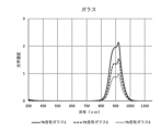
- FIG. 3 is a diagram showing spectral transmittance curves of Yb-containing glasses 1 to 3 and alkali glass.
- FIG. 4 is a diagram showing optical density curves of Yb-containing glasses 1 to 3.
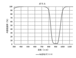
- FIG. 5 is a diagram showing a spectral transmittance curve of the Yb-containing glass 4.
- FIG. 6 is a diagram showing an optical density curve of Yb-containing glass 4.
- FIG. 7 is a diagram showing a spectral transmittance curve of ceramics.
- FIG. 8 is a diagram showing an optical density curve of ceramics.
- FIG. 1 is a cross-sectional view schematically showing an example of an optical filter according to an embodiment.
- FIG. 2 is a cross-sectional view schematically showing another example of the optical filter of one embodiment.
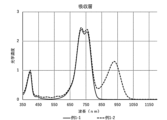
- FIG. 9 is a diagram showing spectral transmittance curves of the absorption layers of Example 1-1 and Example 1-2.
- FIG. 10 is a diagram showing optical density curves of the absorption layers of Example 1-1 and Example 1-2.
- FIG. 11 is a diagram showing a spectral transmittance curve and a spectral reflectance curve of the optical filter of Example 2-1.
- FIG. 12 is a diagram showing the spectral transmittance curve of the optical filter of Example 2-2.
- FIG. 13 is a diagram showing the spectral transmittance curve of the optical filter of Example 2-3.
- FIG. 14 is a diagram showing the spectral transmittance curve and spectral reflectance curve of the optical filter of Example 2-4.
- FIG. 15 is a diagram showing the spectral transmittance curve of the optical filter of Example 2-5.
- FIG. 16 is a diagram showing the spectral transmittance curve of the optical filter of Example 2-6.
- FIG. 17 is a diagram showing the spectral transmittance curve of the optical filter of Example 2-7.
- FIG. 18 is a diagram showing the spectral transmittance curve of the optical filter of Example 2-8.
- NIR dyes near-infrared absorbing dyes
- UV dyes ultraviolet absorbing dyes
- the compound represented by formula (I) is referred to as compound (I).
- the dye composed of compound (I) is also referred to as dye (I), and the same applies to other dyes.
- the group represented by formula (I) is also referred to as group (I), and the same applies to groups represented by other formulas.
- internal transmittance refers to the ratio of measured transmittance to interface reflection, which is expressed by the formula ⁇ actually measured transmittance (incident angle 0 degrees)/(100-reflectance (incident angle 5 degrees)) ⁇ 100. This is the transmittance obtained by subtracting the influence.
- optical density indicates a value converted from internal transmittance using the following formula.
- Optical density at wavelength ⁇ nm -log10 (iT ⁇ /100) iT ⁇ : Internal transmittance at an incident angle of 0 degrees at a wavelength of ⁇ nm
- transmittance Internal transmittance
- the transmittance measured by dissolving a dye in a solvent such as dichloromethane, the transmittance of a dielectric multilayer film, and the transmittance of an optical filter having a dielectric multilayer film are actually measured transmittances.
- a transmittance of 90% or more means that the transmittance is not less than 90% in the entire wavelength range, that is, the minimum transmittance is 90% or more in that wavelength range. means.
- a transmittance of 1% or less means that the transmittance does not exceed 1% in the entire wavelength range, that is, the maximum transmittance in that wavelength range is 1% or less.
- the average transmittance and average internal transmittance in a specific wavelength range are the arithmetic averages of the transmittance and internal transmittance for every 1 nm in the wavelength range. Spectral properties can be measured using a UV-visible spectrophotometer. In this specification, " ⁇ " representing a numerical range includes the upper and lower limits.
- An optical filter according to an embodiment of the present invention includes an absorber made of an inorganic material containing ytterbium, and an absorber containing a dye and resin having a maximum absorption wavelength between 350 nm and 1200 nm. layer, and a dielectric multilayer film. Due to the reflection characteristics of the dielectric multilayer film and the absorption characteristics of the absorber and absorption layer, the optical filter as a whole has excellent transparency in the visible light region and a specific near-infrared light region, and excellent transparency in other near-infrared light regions. Excellent shielding performance can be achieved.
- FIG. 1 and 2 are cross-sectional views schematically showing an example of an optical filter according to an embodiment.
- the optical filter 1A shown in FIG. 1 includes an absorber 10 made of an inorganic material containing ytterbium, a dielectric multilayer film 21 laminated on one main surface of the absorber 10, and a dielectric multilayer film 21 laminated on the other main surface of the absorber 10.
- the optical filter 1B shown in FIG. 2 is an example in which a dielectric multilayer film 22 is further provided on the surface of the absorption layer 30.
- ⁇ Absorber> Equipped with an absorber made of an inorganic material containing ytterbium.
- Inorganic materials containing ytterbium have excellent transparency in the visible light region and in the near-infrared light region from visible light to about 800 nm, and in the near-infrared light region after 850 nm, especially in the near-infrared light region from 900 to 1000 nm. Absorbs external light. Furthermore, since light is blocked by absorption characteristics, the light blocking property is not affected by the incident angle, unlike a dielectric multilayer film.
- an inorganic material containing ytterbium especially when the sensing wavelength range is 800 to 900 nm, it has excellent transparency in the near-infrared light region even at high incident angles, and it is possible to achieve excellent transparency in the near-infrared light region even at high incident angles, and to An optical filter can be obtained in which the spectral transmittance curve of the boundary region between the two regions is less likely to shift depending on the angle of incidence, and is less susceptible to the influence of the angle of incidence.
- the inorganic material containing ytterbium has a steep absorption band, it is possible to maintain high transmittance in a region other than the maximum absorption wavelength region.
- the optical filter described in Patent Document 1 mentioned above since the wavelength side longer than the sensing wavelength region is blocked mainly by the absorption ability of the near-infrared light absorbing dye, the transmittance of the sensing wavelength is also reduced. There is a risk.
- the absorber preferably satisfies the following spectral characteristics (iii-1).
- (iii-1) Average optical density OD 940-960_AVE at wavelength 940 nm to 960 nm / Average optical density OD 840-860_AVE at wavelength 840 nm to 860 nm >5
- the ratio of the spectral characteristic (iii-1) increases as the average transmittance in the wavelength range of 840 nm to 860 nm increases and as the average transmittance in the wavelength range of 940 nm to 960 nm decreases.
- the absorber sufficiently transmits near-infrared light with a wavelength of 840 nm to 860 nm and sufficiently absorbs near-infrared light with a wavelength of 940 nm to 960 nm. means.
- the ratio of spectral characteristics (iii-1) is more preferably 10 or more, and even more preferably 20 or more.
- the absorber satisfies the following spectral characteristics (iii-2).
- (iii-2) Average optical density OD 920-930_AVE at wavelength 920 nm to 930 nm / Average optical density OD 870-880_AVE at wavelength 870 nm to 880 nm >3
- the ratio of the spectral characteristic (iii-2) is more preferably 5 or more, still more preferably 7 or more.
- the absorber satisfies the following spectral characteristics (iii-3).
- (iii-3) Optical density OD 1000 at wavelength 1000 nm / Optical density OD 800 at wavelength 800 nm >10
- the ratio of spectral characteristic (iii-3) increases as the transmittance at a wavelength of 800 nm increases and the transmittance at a wavelength of 1000 nm decreases.
- a ratio of spectral characteristic (iii-3) greater than 10 means that the absorber sufficiently transmits near-infrared light with a wavelength of around 800 nm and sufficiently absorbs near-infrared light with a wavelength of around 1000 nm. do.
- the ratio of spectral characteristics (iii-3) is more preferably 50 or more.
- Examples of inorganic materials containing ytterbium include single crystal and polycrystalline sintered bodies such as Yb 2 O 3 , Yb:YAG (yttrium aluminum garnet), and Yb:YVO 4 , and glass containing ytterbium.
- glass containing ytterbium is more preferable from the viewpoint of processability, stability of material quality, and ease of adjusting physical properties.
- the ytterbium-containing glass preferably has a maximum absorption wavelength of 940 nm to 1000 nm.
- the average internal transmittance of the ytterbium-containing glass at a wavelength of 450 nm to 600 nm and an incident angle of 0 degrees is preferably 60% or more, more preferably 80% or more, and even more preferably 90% or more.
- the average internal transmittance of the ytterbium-containing glass at a wavelength of 700 nm to 800 nm and an incident angle of 0 degrees is preferably 60% or more, more preferably 80% or more, and still more preferably 90% or more.
- Examples of the ytterbium-containing glass include glasses having any of the following compositions.
- a glass further contains SiO 2 as an essential component, and the SiO 2 content is 5 mol% to 35 mol%.
- a glass further contains La 2 O 3 as an essential component, and the content of La 2 O 3 is 1 mol% to 20 mol%.
- ytterbium-containing glass commercially available products may be used, and it can be produced by known methods described in Japanese Patent Application Laid-open No. 61-163138 and Japanese Patent Application Publication No. 56-78447.
- ytterbium-containing glass is a glass containing an alkali metal, and alkali metal ions (for example, Li ions, Na ions) with alkali ions having a larger ionic radius (for example, Na ions or K ions for Li ions, and K ions for Na ions). May be used.
- alkali metal ions for example, Li ions, Na ions
- alkali ions having a larger ionic radius for example, Na ions or K ions for Li ions, and K ions for Na ions.
- the inorganic material containing ytterbium is a single crystal or polycrystalline sintered body containing ytterbium
- these single crystal or polycrystalline sintered bodies contain 10 mol% or more of Yb 2 O 3 in mol% based on oxide.
- the amount of Yb included or doped is 10 at % or more in terms of the composition ratio of Yb and the element in the base material to be substituted.
- YAG since Y in Y 3 Al 5 O 12 is substituted with Yb, it is preferable that [Yb/(Yb+Y)] ⁇ 100 is 10 at % or more.
- the shape of the absorber is preferably a flat plate, a wedge-shaped flat plate, a curved shape with a constant thickness, or a lens shape with a thickness deviation, from the viewpoint of functioning as a support that maintains the shape of the optical filter.
- it is flat.
- the thickness of the absorber is preferably 3 mm or less, more preferably 2 mm or less, and even more preferably 1 mm or less, from the viewpoint of ease of optical design when incorporated into the camera module, and from the viewpoint of element strength and desired optical properties.
- the diameter is preferably 0.1 mm or more.
- the present filter includes an absorption layer containing a resin and a dye having a maximum absorption wavelength between 350 nm and 1200 nm. Thereby, the area where light is not blocked by the reflective property of the dielectric multilayer film can be compensated for by the absorption property of the dye.
- the absorption region of the absorber made of inorganic material containing ytterbium is mainly from 900 to 1000 nm
- various bandpass filters can be designed by appropriately selecting the maximum absorption wavelength region of the dye. can.
- the dye in the absorption layer is a near-infrared light-absorbing dye that has a maximum absorption wavelength in a wavelength region shorter than 800 nm
- a dual layer that selectively transmits visible light and near-infrared light in the range of 800 to 900 nm may be used.
- a passband filter is obtained.
- the dye in the absorption layer is a near-infrared light absorbing dye (hereinafter also referred to as "dye X 800S ”) having a maximum absorption wavelength in a wavelength region shorter than 800 nm will be described.
- the absorption layer containing the dye X 800S preferably satisfies all of the following spectral characteristics (ii-1) to (ii-2).
- (ii-1) The shortest wavelength at which the internal transmittance is 30% in the spectral transmittance curve of wavelengths 650 to 720 nm is ⁇ A_VIS (30%) , and the internal transmittance is 30% in the spectral transmittance curve of wavelengths 720 to 1000 nm.
- the maximum absorption wavelength should be in the range of 680 to 740 nm.
- a certain dye may be combined with a dye having a wavelength of 740 to 800 nm.
- squarylium dyes may be used from the viewpoint of realizing a wide range of absorption with a small amount added.
- Characteristic (ii-2) means that the absorption layer has both high visible light transmittance at 450 nm and high near-infrared light shielding property at 720 nm.
- OD_720 - OD_450 is preferably 1.5 or more, more preferably 2 or more.
- a symmetrical squarylium dye may be used as a near-infrared absorbing dye, from the viewpoint of strongly absorbing around 720 nm and maintaining high transmittance in the visible light region. .
- the dye X 800S is preferably a dye (hereinafter also referred to as "NIR dye") having a maximum absorption wavelength in the wavelength range of 680 to 800 nm in dichloromethane.
- NIR dye a dye having a maximum absorption wavelength in the wavelength range of 680 to 800 nm in dichloromethane.
- the absorption layer can absorb a wide range of near-infrared light absorption bands centered at 720 nm, and absorb visible light at 450 nm, as shown in characteristics (ii-1) and (ii-2) above. It is easy to achieve both transparency and near-infrared light shielding property of 720 nm.
- two types of dyes with different maximum absorption wavelengths in the range of 680 to 800 nm should be combined, preferably a dye with a maximum absorption wavelength in the range of 680 to 740 nm and a dye in the range of 740 to 800 nm. It is preferable to combine them.
- NIR dyes include squarylium dyes, cyanine dyes, phthalocyanine dyes, naphthalocyanine dyes, dithiol metal complex dyes, azo dyes, polymethine dyes, phthalide dyes, naphthoquinone dyes, anthraquinone dyes, indophenol dyes, pyrylium dyes, thiopyrylium dyes, At least one kind selected from the group consisting of quinceconium dyes, tetradehyde ocholine dyes, phenylmethane dyes, aminium dyes, and diimmonium dyes is preferred.
- the NIR dye preferably contains at least one dye selected from squarylium dyes, phthalocyanine dyes, and cyanine dyes.
- squarylium dyes and cyanine dyes are preferable from a spectral point of view, and phthalocyanine dyes are preferable from a durability point of view.
- the content of the NIR dye in the absorption layer is preferably 0.1 to 25 parts by weight, more preferably 0.3 to 15 parts by weight, based on 100 parts by weight of the resin. Note that when two or more types of compounds are combined, the above content is the sum of each compound.
- the absorption layer may contain other dyes in addition to the above NIR dyes.
- a dye (UV dye) having a maximum absorption wavelength in the resin from 370 to 440 nm is preferable. Thereby, the near-ultraviolet light region can be efficiently blocked.
- UV dyes examples include oxazole dyes, merocyanine dyes, cyanine dyes, naphthalimide dyes, oxadiazole dyes, oxazine dyes, oxazolidine dyes, naphthalic acid dyes, styryl dyes, anthracene dyes, cyclic carbonyl dyes, triazole dyes, and the like.
- merocyanine dyes are particularly preferred.
- one type may be used alone, or two or more types may be used in combination.
- the absorbent layer is preferably laminated on at least one main surface of the absorber. Since the absorber is an inorganic material as described above, it can have both near-infrared light absorption ability and the function as a support.
- the resin in the absorption layer is not limited as long as it is a transparent resin, and examples include polyester resin, acrylic resin, epoxy resin, ene-thiol resin, polycarbonate resin, polyether resin, polyarylate resin, polysulfone resin, polyethersulfone resin, One or more transparent resins selected from polyparaphenylene resin, polyarylene ether phosphine oxide resin, polyamide resin, polyimide resin, polyamideimide resin, polyolefin resin, cyclic olefin resin, polyurethane resin, polystyrene resin, etc. are used. These resins may be used alone or in combination of two or more. From the viewpoint of the spectral characteristics, glass transition point (Tg), and adhesiveness of the absorption layer, one or more resins selected from polyimide resins, polycarbonate resins, polyester resins, and acrylic resins are preferred.
- NIR dyes or other dyes these may be contained in the same absorption layer, or may be contained in separate absorption layers.
- the absorption layer is prepared by preparing a coating solution by dissolving or dispersing the dye, resin or raw material components of the resin, and each component added as necessary in a solvent, and coating this on a support and drying it. It can be further formed by hardening as needed.
- the support may be the above-mentioned absorbent material, or may be a peelable support used only when forming the resin film.
- the solvent may be any dispersion medium that can be stably dispersed or a solvent that can be dissolved.
- the coating liquid may also contain a surfactant to improve voids caused by microbubbles, dents caused by adhesion of foreign substances, and repellency during the drying process.
- a dip coating method, a cast coating method, a spin coating method, or the like can be used for applying the coating liquid.
- a curing treatment such as thermal curing or photocuring is further performed.
- the absorbent layer can be manufactured into a film by extrusion molding.
- the present filter can be manufactured by laminating the obtained film-like absorbent layer on an absorbent body and integrating the absorbent layer by thermocompression bonding or the like.
- the optical filter may have one absorption layer, or two or more absorption layers.
- each layer may have the same or different configurations, and may be formed on each surface of the dielectric multilayer film, or two or more layers may be stacked on the surface of one dielectric multilayer film.
- the thickness of the absorption layer is 10 ⁇ m or less, preferably 5 ⁇ m or less from the viewpoint of in-plane film thickness distribution within the substrate after coating and appearance quality, and from the viewpoint of expressing desired spectral characteristics at an appropriate dye concentration. It is preferably 0.5 ⁇ m or more.
- the total thickness of each absorption layer is within the said range.
- This filter includes a dielectric multilayer film.
- This filter may have one or more dielectric multilayer films, but at least one is designed as a reflective film that reflects a portion of near-infrared light (hereinafter also referred to as "NIR reflective film”). It is preferable.
- Other dielectric multilayer films may be designed as reflective layers or antireflection layers having a reflection region other than the near-infrared region.
- the NIR reflective layer has wavelength selectivity, for example, to transmit visible light, transmit near-infrared light in the transmission region of the absorption layer, and mainly reflect other near-infrared light.
- the NIR reflective layer may be appropriately designed to further reflect light in a wavelength range other than near-infrared light, for example, near-ultraviolet light.
- a dielectric multilayer film designed as an NIR reflective layer preferably satisfies the following spectral characteristics.
- the average reflectance R D_450-600AVE in the spectral reflectance curve of the optical filter at a wavelength of 450 to 600 nm and an incident angle of 5 degrees is 3% or less
- the average reflectance R D_1000 in the spectral reflectance curve of the optical filter at a wavelength of 1000 to 1200 nm and an incident angle of 5 degrees is a dielectric multilayer film designed as a NIR reflective layer.
- the reflection characteristics of the dielectric multilayer film can be appropriately designed so that the optical filter as a whole has a desired transmittance.
- the NIR reflective layer is composed of, for example, a dielectric multilayer film in which dielectric films with a low refractive index (low refractive index film) and dielectric films with a high refractive index (high refractive index film) are alternately laminated.
- the high refractive index film preferably has a refractive index of 1.6 or more, more preferably 2.2 to 2.5.
- materials for the high refractive index film include Ta 2 O 5 , TiO 2 , and Nb 2 O 5 . Among these, TiO 2 is preferred in terms of film formability, reproducibility in refractive index, stability, and the like.
- the low refractive index film preferably has a refractive index of less than 1.6, more preferably 1.45 or more and less than 1.55.
- the material for the low refractive index film include SiO 2 and SiO x N y .
- SiO 2 is preferred from the viewpoint of reproducibility in film formation, stability, economic efficiency, and the like.
- the NIR reflective layer In order for the NIR reflective layer to transmit visible light and specific near-infrared light, it is possible to combine several types of dielectric multilayer films with different spectral characteristics when transmitting and selecting a desired wavelength band. For example, it can be adjusted by the material constituting the film, the thickness of each layer, and the number of layers.
- the NIR reflective layer preferably has a total number of dielectric multilayer films constituting the reflective layer of 20 or more layers, more preferably 25 or more layers, and a ripple suppression layer. From this point of view, the number of layers is preferably 60 or less.
- the thickness of the dielectric multilayer film is preferably 100 nm or more, more preferably 300 nm or more, from the viewpoint of suppressing deterioration of the absorbing material, and in order to improve productivity and suppress reflection ripples in the visible light region. From this viewpoint, the thickness is preferably 5 ⁇ m or less.
- a vacuum film forming process such as a CVD method, a sputtering method, a vacuum evaporation method, or a wet film forming process such as a spray method or a dip method can be used.
- the NIR reflecting layer may have one layer (a group of dielectric multilayer films) that provides predetermined optical properties, or two layers that provide predetermined optical properties.
- each reflective layer may have the same configuration or different configurations.
- it is usually composed of a plurality of reflective layers with different reflection bands.
- one is a near-infrared reflective layer that blocks light in the short wavelength band of the near-infrared region
- the other is a near-infrared reflective layer that blocks light in the long wavelength band of the near-infrared region and the near-ultraviolet region. It may also be a near-infrared/near-ultraviolet reflective layer that blocks light.
- dielectric multilayers may be designed as antireflection layers.
- the antireflection layer include a dielectric multilayer film, an intermediate refractive index medium, and a moth-eye structure in which the refractive index gradually changes.
- dielectric multilayer films are preferred from the viewpoint of optical efficiency and productivity.
- the antireflection layer is obtained by alternately laminating high refractive index dielectric films and low refractive index dielectric films.
- This filter may also include, as other components, a component (layer) that provides absorption by inorganic fine particles or the like that controls the transmission and absorption of light in a specific wavelength range.
- a component (layer) that provides absorption by inorganic fine particles or the like that controls the transmission and absorption of light in a specific wavelength range.
- inorganic fine particles include ITO (Indium Tin Oxides), ATO (Antimony-doped Tin Oxides), cesium tungstate, lanthanum boride, and the like.
- ITO fine particles and cesium tungstate fine particles have high visible light transmittance and have light absorption properties over a wide range of infrared wavelengths exceeding 1200 nm, so they can be used when such infrared light shielding properties are required. .
- the optical filter of the present invention preferably satisfies the following spectral characteristics.
- (i-1) In the spectral transmittance curve at a wavelength of 450 nm to 600 nm and an incident angle of 0 degrees, the average transmittance T 450-600 (0 deg) AVE is 60% or more satisfying spectral characteristics (i-1). This means that it has excellent transparency in the visible light range of ⁇ 600 nm.
- T 450-600 (0deg) AVE is preferably 80% or more, more preferably 88% or more.
- a dielectric multilayer film having excellent transparency in the visible light region and a dye having excellent transparency in the visible light region may be used.
- the optical filter of the present invention preferably satisfies the following spectral characteristics.
- (i-2) In the spectral transmittance curve at a wavelength of 800 nm to 900 nm and an incident angle of 0 degrees, the maximum transmittance T 800-900 (0deg) MAX is 60% or more satisfying spectral characteristics (i-2). This means that it has excellent transparency in the near-infrared light region of ⁇ 900 nm.
- T 800-900 (0deg) MAX is preferably 70% or more, more preferably 80% or more, even more preferably 85% or more.
- a dielectric multilayer film having excellent transparency in the near-infrared light region of 800 to 900 nm may be used.
- the optical filter of the present invention preferably satisfies the following spectral characteristics.
- (i-3) In the spectral transmittance curve at a wavelength of 930 nm to 950 nm and an incident angle of 0 degrees, the maximum transmittance T 930-950 (0 deg) MAX is 20% or less This means that it has excellent shielding properties in the near-infrared light region of ⁇ 950 nm.
- T 930-950 (0deg) MAX is preferably 16% or less, more preferably 12% or less, even more preferably 8% or less. Further, in order to satisfy the spectral characteristic (i-3), for example, light may be blocked by the absorption ability of the ytterbium-containing inorganic material.
- the optical filter of the present invention preferably satisfies the following spectral characteristics.
- (i-4) In the spectral transmittance curve at a wavelength of 800 nm to 1000 nm and an incident angle of 0 degrees, when the wavelength at which the maximum transmittance occurs is ⁇ 800-1000 (0 deg) MAX , A wavelength ⁇ IRL (0deg) (50%) where the transmittance is 50% in a wavelength range longer than ⁇ 800-1000 (0deg) MAX and at an incident angle of 0 degrees, ⁇ IRL (35 deg) (50%), which is a wavelength longer than 800-1000 (0 deg) MAX and has a transmittance of 50% at an incident angle of 35 degrees, satisfies the following relational expression
- ⁇ 15nm Satisfying the spectral characteristic (i-4) means that the spectral curve in the wavelength range of 800 nm to 1000 nm is less likely to shift
- light may be blocked by the absorption ability of the ytterbium-containing inorganic material.
- the optical filter of the present invention has excellent spectral characteristics, including excellent transmittance of visible light, excellent shielding properties of specific near-infrared light, and small shift of the spectral curve even at high incident angles. .
- the imaging device of the present invention preferably includes the optical filter of the present invention.
- the imaging device further includes a solid-state imaging device and an imaging lens.
- the present invention relates to the following optical filter and the like.
- An absorber made of an inorganic material containing ytterbium, an absorption layer containing a resin and a dye having a maximum absorption wavelength between 350 nm and 1200 nm;
- the absorber is made of glass containing ytterbium, The optical filter according to any one of [1] to [3], wherein the glass contains Yb 2 O 3 in an amount of 10 mol % or more expressed as mol % based on oxides.
- the absorber is made of a single crystal or polycrystalline sintered body containing ytterbium, The single crystal or polycrystalline sintered body contains 10 mol % or more of Yb 2 O 3 in mol % based on oxide, or the doping amount of Yb is different from the element in the base material that replaces Yb.
- An ultraviolet-visible spectrophotometer manufactured by Hitachi High-Technologies Corporation, model UH-4150 was used to measure each spectral characteristic. Note that, unless the incident angle is specified, the spectral characteristics are values measured at an incident angle of 0 degrees (perpendicular to the main surface of the optical filter).
- the dyes used in each example are as follows.
- Compound 1 (squarylium compound): Synthesized based on US Pat. No. 5,543,086.
- Compound 2 squarylium compound: Synthesized based on International Publication No. 2017/135359.
- Compound 3 (merocyanine compound): Synthesized based on German Patent Publication No. 10109243.
- Compound 4 (cyanine compound): Synthesized based on Dyes and Pigments 73 (2007) 344-352.
- Compound 5 (squarylium compound): Synthesized based on Japanese Patent Application Publication No. 2020-31198. Note that Compound 1, Compound 2, Compound 4, and Compound 5 are near-infrared absorbing dyes (NIR dyes), and Compound 3 is a near-ultraviolet absorbing dye (UV dye).
- NIR dyes near-infrared absorbing dyes
- UV dye near-ultraviolet absorbing dye
- Yb ytterbium
- the reflectance curve was measured, and the optical density was calculated from the obtained transmittance.
- the results are shown in the table below. Note that the spectral characteristics shown in the table below were evaluated based on internal transmittance in order to avoid the influence of reflection at the air interface and glass interface.
- Internal transmittance (%) ⁇ Actually measured transmittance (0deg) / (100 - reflectance (5deg) ) ⁇ ⁇ 100
- the spectral transmittance curves of Yb-containing glasses 1 to 3 and alkali glass are shown in FIG. 3
- the optical density curves of Yb-containing glasses 1 to 3 are shown in FIG. 4
- the spectral transmittance curve of Yb-containing glass 4 is shown in FIG.
- the optical density curves of the Yb-containing glass 4 are shown in FIG. 6, respectively.
- Yb:YAG ceramics manufactured by Kamishima Chemical Co., Ltd.
- % here refers to the doping amount of Yb, that is, the composition ratio of Yb to the element in the base material to be substituted, and the unit is at %.
- YAG since Y out of 12 Y 3 Al 5 O is substituted with Yb, it refers to the value of [Yb/(Yb+Y)] ⁇ 100.
- Spectral characteristics of absorption layer Mix any of the dyes of Compounds 1 to 5 to a polyimide resin solution prepared in the same manner as when calculating the spectral characteristics of the above compound at the concentrations listed in the table below, and stir and dissolve at 50 ° C. for 2 hours. A coating solution was thus obtained. The resulting coating solution was applied to alkali glass (manufactured by SCHOTT, D263 glass, thickness 0.2 mm) by a spin coating method to form an absorption layer having the thickness shown in the table below. The spectral transmittance curve and spectral reflectance curve of the obtained absorption layer in the wavelength range of 350 to 1200 nm were measured using an ultraviolet-visible spectrophotometer.
- Example 2-1 Spectral characteristics of optical filter>
- a first dielectric multilayer film (reflective film) was formed by alternately stacking SiO 2 and TiO 2 on one surface of an infrared absorbing glass (Yb-containing glass 1) by vapor deposition.
- Yb-containing glass 1 an infrared absorbing glass
- a resin solution was applied to the surface of the first dielectric multilayer film, and the organic solvent was removed by sufficient heating to form an absorption layer with a thickness of 1.3 ⁇ m.
- a second dielectric multilayer film (antireflection film) was formed on the surface of the absorption layer by alternately stacking SiO 2 and TiO 2 by vapor deposition.
- Example 2-2 Optical filter 2-2 was produced in the same manner as Example 2-1 except that the infrared absorbing glass was changed from Yb-containing glass 1 to Yb-containing glass 2.
- Example 2-3 Optical filter 2-3 was produced in the same manner as Example 2-1 except that the infrared absorbing glass was changed from Yb-containing glass 1 to Yb-containing glass 3.
- Optical filter 2-4 was prepared in the same manner as Example 2-1, except that the infrared absorbing glass (Yb-containing glass 1) was changed to non-absorbing glass (alkali glass, manufactured by SCHOTT, D263, 0.3 mm). Manufactured.
- Example 2-5 The infrared absorbing glass (Yb-containing glass 1) was changed to a non-absorbing glass (alkali glass, made by SCHOTT, D263, 0.2 mm), and the absorption layer was changed from Example 1-1 to Example 1-2 with a thickness of 1.5 ⁇ m.
- Optical filter 2-5 was manufactured in the same manner as Example 2-1 except for the following changes.
- Example 2-6 A first dielectric multilayer film (reflective film) is formed by alternately layering SiO 2 and TiO 2 on one surface of non-absorbing glass (alkali glass, manufactured by SCHOTT, D263, 0.2 mm) by vapor deposition. was formed. A second dielectric multilayer film (antireflection film) was formed on the other surface of the non-absorbing glass by alternately stacking SiO 2 and TiO 2 by vapor deposition. Through the above steps, optical filter 2-6 was manufactured.
- non-absorbing glass alkali glass, manufactured by SCHOTT, D263, 0.2 mm
- Example 2-7 Optical filter 2-7 was manufactured in the same manner as Example 2-1 except that the inorganic material (absorber) was changed from Yb-containing glass 1 to Yb-containing glass 4.
- Example 2-8 Optical filter 2-8 was manufactured in the same manner as Example 2-1 except that the inorganic material (absorber) was changed from Yb-containing glass 1 to 10% Yb:YAG ceramics.
- the table below shows the reflectance of each of the above optical filters when measured using the first dielectric multilayer film as the incident surface.
- the spectral transmittance curve at an incident angle of 0 degrees and 35 degrees in the wavelength range of 350 to 1200 nm and the spectral reflection at an incident angle of 5 degrees were determined using a UV-visible spectrophotometer. The rate curve was measured. From the obtained spectral characteristic data, the characteristics shown in Tables 6 and 7 below were calculated. Further, spectral transmittance (reflectance) curves of the optical filters of Examples 2-1 to 2-8 are shown in FIGS. 11 to 18, respectively.
- Examples 2-1 to 2-3 and Examples 2-7 to 2-8 are examples, and Examples 2-4 to 2-6 are comparative examples.
- the optical filters of Examples 2-1, 2-2, and 2-3 have excellent transmittance for visible light and near-infrared light of 800 to 1000 nm, especially 800 to 900 nm, and It can be seen that this optical filter has excellent light-shielding properties for external light, especially in the wavelength range of 1050 to 1200 nm, and also has a small shift in the spectral curve even at high incident angles.
- the optical filter of Example 2-6 which does not use ytterbium-containing glass or near-infrared light-absorbing dye and blocks part of the near-infrared light region only by the reflection characteristics of the dielectric multilayer film, has
- the optical filters of Examples 2-7 and 8 also have excellent transmittance for visible light and near-infrared light of 800 to 1000 nm, especially 800 to 900 nm, and have excellent transparency for other near-infrared light, especially 1050 nm. It can be seen that this optical filter has excellent light blocking properties in the wavelength region of ⁇ 1200 nm, and further shows a small shift in the spectral curve even at high incident angles.
- the optical filter of the present invention has excellent visible light transmittance and has specific near-infrared light shielding properties. In recent years, performance has been increasing, and it is useful for information acquisition devices such as cameras and sensors for transportation aircraft.
Landscapes
- Physics & Mathematics (AREA)
- Chemical & Material Sciences (AREA)
- General Physics & Mathematics (AREA)
- Optics & Photonics (AREA)
- Engineering & Computer Science (AREA)
- Materials Engineering (AREA)
- Organic Chemistry (AREA)
- Life Sciences & Earth Sciences (AREA)
- Chemical Kinetics & Catalysis (AREA)
- General Chemical & Material Sciences (AREA)
- Geochemistry & Mineralogy (AREA)
- Optical Filters (AREA)
Abstract
本発明は、イッテルビウムを含む無機材料からなる吸収体と、350nm~1200nmの間に最大吸収波長を有する色素と樹脂とを含む吸収層と、誘電体多層膜とを備えた光学フィルタに関する。
Description
本発明は、可視光領域を透過し、特定の近赤外光領域を遮断する光学フィルタに関する。
固体撮像素子を用いた撮像装置には、監視カメラや車載カメラ等、昼夜を問わず撮像する装置にまでその用途を拡げている。このような装置では、可視光に基づく(カラー)画像と赤外光に基づく(白黒)画像をそれぞれ取得する必要がある。
このため、可視光を透過させ、該可視光に基づく画像を忠実に再現するための近赤外線カットフィルタ機能に加え、特定の近赤外光を選択的に透過させる機能を備えた光学フィルタ、いわゆるデュアルバンドパスフィルタの使用が検討されている。
特許文献1には、誘電体多層膜と近赤外線吸収色素を含む樹脂基材とを組み合わせた、可視光と850nm付近の近赤外光を透過し、それ以外の光を遮断する光学フィルタが記載されている。
また、特許文献2には、誘電体多層膜と近赤外線吸収色素を含む樹脂基材とを組み合わせた、可視光と800nm付近の近赤外光を透過し、それ以外の光を遮断する光学フィルタが記載されている。
近年、イメージング分野のセンサでは800~1000nmの一部の領域を含むレーザー光が用いられるため、かかるセンシング領域の近赤外光を透過でき、ノイズとなるそれ以外の近赤外光を遮断できる光学フィルタが求められている。
また、誘電体多層膜を有する光学フィルタは、光の入射角度により誘電体多層膜の光学膜厚が変化するために、入射角による分光透過率曲線の変化が問題である。例えば、光の入射角度が大きくなると反射特性が短波長側にシフトする結果、本来遮蔽したい領域において反射特性が低下するおそれがある。かかる現象は入射角度が大きいほど強く発生しやすい。このようなフィルタを使用すると、固体撮像素子の分光感度が入射角の影響を受けるおそれがある。近年のカメラモジュール低背化に伴い高入射角条件での使用が想定されるため、入射角の影響を受けにくい光学フィルタが求められている。
可視光透過領域や、短波側近赤外遮光領域から近赤外透過領域に切り替わる領域におけるシフトは色素等の吸収材料を用いることでシフトを低減することができる。一方で近赤外光透過領域から長波側近赤外光遮光領域に切り替わる領域は吸収材料によってシフトを低減することが難しい。この領域のみシフトが大きい場合には、入射角度により近赤外光の透過光量が変化してしまい、固体撮像素子における可視光と赤外光の取り込み光量の比率も入射角により変化することになる。その結果可視光に基づく(カラー)画像の色再現性や、赤外光に基づく(白黒)画像の再現性に影響を及ぼすことが懸念される。
この点、特許文献2に記載の光学フィルタは、高入射角の光に対する分光曲線のシフト低減の点で改善の余地がある。
本発明は、可視光の透過性に優れ、特定の近赤外光の遮蔽性に優れ、高入射角においても分光曲線のシフトが小さい光学フィルタの提供を目的とする。
本発明は、以下の構成を有する光学フィルタを提供する。
〔1〕イッテルビウムを含む無機材料からなる吸収体と、
350nm~1200nmの間に最大吸収波長を有する色素と樹脂とを含む吸収層と、
誘電体多層膜とを備えた光学フィルタ。
〔1〕イッテルビウムを含む無機材料からなる吸収体と、
350nm~1200nmの間に最大吸収波長を有する色素と樹脂とを含む吸収層と、
誘電体多層膜とを備えた光学フィルタ。
本発明によれば、高入射角においても、可視光の透過性に優れ、特定の近赤外光の遮蔽性に優れた光学フィルタが提供できる。本発明の光学フィルタは、特に、高入射角においてもセンシング波長領域である800~1000nmの近赤外光領域の透過領域と、遮蔽したい長波長側の波長領域との境界領域の分光透過率曲線が入射角度によってシフトしにくく、入射角の影響を受けにくい光学フィルタである。
以下、本発明の実施の形態について説明する。
本明細書において、近赤外線吸収色素を「NIR色素」、紫外線吸収色素を「UV色素」と略記することもある。
本明細書において、式(I)で示される化合物を化合物(I)という。他の式で表される化合物も同様である。化合物(I)からなる色素を色素(I)ともいい、他の色素についても同様である。また、式(I)で表される基を基(I)とも記し、他の式で表される基も同様である。
本明細書において、近赤外線吸収色素を「NIR色素」、紫外線吸収色素を「UV色素」と略記することもある。
本明細書において、式(I)で示される化合物を化合物(I)という。他の式で表される化合物も同様である。化合物(I)からなる色素を色素(I)ともいい、他の色素についても同様である。また、式(I)で表される基を基(I)とも記し、他の式で表される基も同様である。
本明細書において、内部透過率とは、{実測透過率(入射角0度)/(100-反射率(入射角5度))}×100の式で示される、実測透過率から界面反射の影響を引いて得られる透過率である。
本明細書において、光学濃度は下記式より内部透過率から換算した値を示す。
波長λnmにおける光学濃度=-log10(iTλ/100)
iTλ:波長λnmにおける入射角0度での内部透過率
本明細書において、ガラスの透過率、色素が樹脂に含有される場合を含む吸収層の透過率の分光は、「透過率」と記載されている場合も全て「内部透過率」である。一方、色素をジクロロメタン等の溶媒に溶解して測定される透過率、誘電体多層膜の透過率、誘電体多層膜を有する光学フィルタの透過率は、実測透過率である。
本明細書において、光学濃度は下記式より内部透過率から換算した値を示す。
波長λnmにおける光学濃度=-log10(iTλ/100)
iTλ:波長λnmにおける入射角0度での内部透過率
本明細書において、ガラスの透過率、色素が樹脂に含有される場合を含む吸収層の透過率の分光は、「透過率」と記載されている場合も全て「内部透過率」である。一方、色素をジクロロメタン等の溶媒に溶解して測定される透過率、誘電体多層膜の透過率、誘電体多層膜を有する光学フィルタの透過率は、実測透過率である。
本明細書において、特定の波長域について、透過率が例えば90%以上とは、その全波
長領域において透過率が90%を下回らない、すなわちその波長領域において最小透過率が90%以上であることをいう。同様に、特定の波長域について、透過率が例えば1%以下とは、その全波長領域において透過率が1%を超えない、すなわちその波長領域において最大透過率が1%以下であることをいう。内部透過率においても同様である。特定の波長域における平均透過率および平均内部透過率は、該波長域の1nm毎の透過率および内部透過率の相加平均である。
分光特性は、紫外可視分光光度計を用いて測定できる。
本明細書において、数値範囲を表す「~」では、上下限を含む。
長領域において透過率が90%を下回らない、すなわちその波長領域において最小透過率が90%以上であることをいう。同様に、特定の波長域について、透過率が例えば1%以下とは、その全波長領域において透過率が1%を超えない、すなわちその波長領域において最大透過率が1%以下であることをいう。内部透過率においても同様である。特定の波長域における平均透過率および平均内部透過率は、該波長域の1nm毎の透過率および内部透過率の相加平均である。
分光特性は、紫外可視分光光度計を用いて測定できる。
本明細書において、数値範囲を表す「~」では、上下限を含む。
<光学フィルタ>
本発明の一実施形態の光学フィルタ(以下、「本フィルタ」ともいう)は、イッテルビウムを含む無機材料からなる吸収体と、350nm~1200nmの間に最大吸収波長を有する色素と樹脂とを含む吸収層と、誘電体多層膜とを備える。
誘電体多層膜の反射特性と、吸収体と吸収層の吸収特性とにより、光学フィルタ全体として可視光領域および特定の近赤外光領域の優れた透過性と、他の近赤外光領域の優れた遮蔽性を実現できる。
本発明の一実施形態の光学フィルタ(以下、「本フィルタ」ともいう)は、イッテルビウムを含む無機材料からなる吸収体と、350nm~1200nmの間に最大吸収波長を有する色素と樹脂とを含む吸収層と、誘電体多層膜とを備える。
誘電体多層膜の反射特性と、吸収体と吸収層の吸収特性とにより、光学フィルタ全体として可視光領域および特定の近赤外光領域の優れた透過性と、他の近赤外光領域の優れた遮蔽性を実現できる。
図面を用いて本フィルタの構成例について説明する。図1~2は、一実施形態の光学フィルタの一例を概略的に示す断面図である。
図1に示す光学フィルタ1Aは、イッテルビウムを含む無機材料からなる吸収体10と、吸収体10の一方の主面に積層された誘電体多層膜21と、吸収体10の他方の主面に設けられた吸収層30を備えた例である。
図2に示す光学フィルタ1Bは、吸収層30の表面に誘電体多層膜22をさらに備えた例である。
<吸収体>
イッテルビウムを含む無機材料からなる吸収体を備える。イッテルビウムを含む無機材料は、可視光領域の透過性と、可視光から800nm程度の近赤外光領域にかけての透過性とに優れ、850nm以降の近赤外光領域、特に900~1000nmの近赤外光領域を吸収する。また、吸収特性により遮光するため、誘電体多層膜と異なり遮光性が入射角の影響を受けない。よってイッテルビウムを含む無機材料を用いることで、特にセンシング波長領域が800~900nmである場合、高入射角においても近赤外光領域の透過性に優れ、かかる透過領域と、遮蔽したい900nm以降の波長領域との境界領域の分光透過率曲線が入射角度によってシフトしにくく、入射角の影響を受けにくい光学フィルタが得られる。
イッテルビウムを含む無機材料からなる吸収体を備える。イッテルビウムを含む無機材料は、可視光領域の透過性と、可視光から800nm程度の近赤外光領域にかけての透過性とに優れ、850nm以降の近赤外光領域、特に900~1000nmの近赤外光領域を吸収する。また、吸収特性により遮光するため、誘電体多層膜と異なり遮光性が入射角の影響を受けない。よってイッテルビウムを含む無機材料を用いることで、特にセンシング波長領域が800~900nmである場合、高入射角においても近赤外光領域の透過性に優れ、かかる透過領域と、遮蔽したい900nm以降の波長領域との境界領域の分光透過率曲線が入射角度によってシフトしにくく、入射角の影響を受けにくい光学フィルタが得られる。
さらに、イッテルビウムを含む無機材料は、吸収帯が急峻であるため、最大吸収波長領域以外の領域の透過性を高く保持できる。一方、前述の特許文献1に記載の光学フィルタは、センシング波長領域よりも長波長側を、主に近赤外光吸収色素の吸収能により遮光しているため、センシング波長の透過性も低下するおそれがある。
吸収体は、下記分光特性(iii-1)を満たすことが好ましい。
(iii-1)波長940nm~960nmにおける平均光学濃度OD940-960_AVE/波長840nm~860nmにおける平均光学濃度OD840-860_AVE>5
(iii-1)波長940nm~960nmにおける平均光学濃度OD940-960_AVE/波長840nm~860nmにおける平均光学濃度OD840-860_AVE>5
分光特性(iii-1)の比率は、波長840nm~860nmにおける平均透過率が大きく、波長940nm~960nmにおける平均透過率が小さいほど、大きくなる。分光特性(iii-1)の比率が5より大きいことで、吸収体が、波長840nm~860nmの近赤外光を十分に透過し、波長940nm~960nmの近赤外光を十分に吸収することを意味する。分光特性(iii-1)の比率は、より好ましくは10以上、さらに好ましくは20以上である。
吸収体は、下記分光特性(iii-2)を満たすことがさらに好ましい。
(iii-2)波長920nm~930nmにおける平均光学濃度OD920-930_AVE/波長870nm~880nmにおける平均光学濃度OD870-880_AVE>3
分光特性(iii-2)の比率は、より好ましくは5以上、さらに好ましくは7以上である。
(iii-2)波長920nm~930nmにおける平均光学濃度OD920-930_AVE/波長870nm~880nmにおける平均光学濃度OD870-880_AVE>3
分光特性(iii-2)の比率は、より好ましくは5以上、さらに好ましくは7以上である。
吸収体は、下記分光特性(iii-3)を満たすことがさらに好ましい。
(iii-3)波長1000nmにおける光学濃度OD1000/波長800nmにおける光学濃度OD800>10
分光特性(iii-3)の比率は、波長800nmにおける透過率が大きく、波長1000nmにおける透過率が小さいほど、大きくなる。分光特性(iii-3)の比率が10より大きいことで、吸収体が、波長800nm付近の近赤外光を十分に透過し、波長1000nm付近の近赤外光を十分に吸収することを意味する。分光特性(iii-3)の比率は、より好ましくは50以上である。
(iii-3)波長1000nmにおける光学濃度OD1000/波長800nmにおける光学濃度OD800>10
分光特性(iii-3)の比率は、波長800nmにおける透過率が大きく、波長1000nmにおける透過率が小さいほど、大きくなる。分光特性(iii-3)の比率が10より大きいことで、吸収体が、波長800nm付近の近赤外光を十分に透過し、波長1000nm付近の近赤外光を十分に吸収することを意味する。分光特性(iii-3)の比率は、より好ましくは50以上である。
イッテルビウムを含む無機材料としては、Yb2O3、Yb:YAG(イットリウム・アルミニウム・ガーネット)、Yb:YVO4等の単結晶および多結晶焼結体や、イッテルビウムを含むガラス等が考えられる。その中でも加工性、材料品質の安定性、物性の調整しやすさの観点からイッテルビウムを含むガラスであることがより好ましい。
イッテルビウム含有ガラスは、最大吸収波長が940nm~1000nmであることが好ましい。
イッテルビウム含有ガラスは、波長450nm~600nmおよび入射角0度での内部透過率の平均が好ましくは60%以上、より好ましくは80%以上、さらに好ましくは90%以上であることが好ましい。
イッテルビウム含有ガラスは、波長700nm~800nmおよび入射角0度での内部透過率の平均が好ましくは60%以上、より好ましくは80%以上、さらに好ましくは90%以上であることが好ましい。
イッテルビウム含有ガラスは、波長450nm~600nmおよび入射角0度での内部透過率の平均が好ましくは60%以上、より好ましくは80%以上、さらに好ましくは90%以上であることが好ましい。
イッテルビウム含有ガラスは、波長700nm~800nmおよび入射角0度での内部透過率の平均が好ましくは60%以上、より好ましくは80%以上、さらに好ましくは90%以上であることが好ましい。
イッテルビウム含有ガラスとしては、例えば、下記いずれかの組成を有するガラスが挙げられる。
(1)酸化物基準のモル%表示で、Yb2O3、B2O3を必須成分として含有し、Yb2O3の含有量が10mol%~60mol%、B2O3の含有量が10mol%~70mol%であるガラス。
(2)(1)に加えてさらにSiO2を必須成分として含有し、SiO2の含有量が5mol%~35mol%であるガラス。
(3)(1)および(2)に加えてさらにLa2O3を必須成分として含有し、La2O3の含有量が1mol%~20mol%であるガラス。
(1)酸化物基準のモル%表示で、Yb2O3、B2O3を必須成分として含有し、Yb2O3の含有量が10mol%~60mol%、B2O3の含有量が10mol%~70mol%であるガラス。
(2)(1)に加えてさらにSiO2を必須成分として含有し、SiO2の含有量が5mol%~35mol%であるガラス。
(3)(1)および(2)に加えてさらにLa2O3を必須成分として含有し、La2O3の含有量が1mol%~20mol%であるガラス。
イッテルビウム含有ガラスとしては、市販品を用いてもよく、日本国特開昭61-163138号公報および日本国特開昭56-78447号公報等に記載される公知の方法から製造できる。
また、イッテルビウム含有ガラスとしては、アルカリ金属を含有する組成のガラスでガラス転移点以下の温度で、イオン交換により、ガラス板主面に存在するイオン半径が小さいアルカリ金属イオン(例えば、Liイオン、Naイオン)を、イオン半径のより大きいアルカリイオン(例えば、Liイオンに対してはNaイオンまたはKイオンであり、Naイオンに対してはKイオンである。)に交換して得られる化学強化ガラスを使用してもよい。
イッテルビウムを含む無機材料がイッテルビウムを含む単結晶または多結晶焼結体である場合、これらの単結晶または多結晶焼結体は、酸化物基準のモル%表示で、Yb2O3を10mol%以上含むか、または、Ybのドープ量が、Ybと置換する母材中の元素との組成比で、10at%以上であることが好ましい。
たとえば、YAGの場合は、Y3Al5O12のうちのYがYbと置換するため、[Yb/(Yb+Y)]×100が10at%以上であることが好ましい。
たとえば、YAGの場合は、Y3Al5O12のうちのYがYbと置換するため、[Yb/(Yb+Y)]×100が10at%以上であることが好ましい。
吸収体の形状は、光学フィルタの形状を保つ支持体としての機能を兼ね備える観点から、平板状、くさび型の平板状、厚みが一定である曲面状、肉厚偏差のあるレンズ形状が好ましく、特に平板状であることが好ましい。
吸収体は、カメラモジュールに組み込む際の光学設計のしやすさの観点から厚さが好ましくは3mm以下、より好ましくは2mm以下、さらに好ましくは1mm以下であり、素子強度の観点や所望の光学特性を得る必要性から、好ましくは0.1mm以上である。
<吸収層>
本フィルタは、350nm~1200nmの間に最大吸収波長を有する色素と樹脂とを含む吸収層を備える。これにより、誘電体多層膜の反射特性で遮光しない領域を色素の吸収特性で補うことができる。
また、上記のイッテルビウムを含む無機材料からなる吸収体の吸収領域が主に900~1000nmであることを考慮して、色素の最大吸収波長領域を適宜選択することで、種々のバンドパスフィルタを設計できる。
本フィルタは、350nm~1200nmの間に最大吸収波長を有する色素と樹脂とを含む吸収層を備える。これにより、誘電体多層膜の反射特性で遮光しない領域を色素の吸収特性で補うことができる。
また、上記のイッテルビウムを含む無機材料からなる吸収体の吸収領域が主に900~1000nmであることを考慮して、色素の最大吸収波長領域を適宜選択することで、種々のバンドパスフィルタを設計できる。
たとえば、吸収層における色素が、800nmより短波長領域に最大吸収波長を有する近赤外光吸収色素であれば、可視光と、800~900nmの近赤外光とを選択的に透過する、デュアルパスバンドフィルタが得られる。
以下、吸収層における色素が、800nmより短波長領域に最大吸収波長を有する近赤外光吸収色素(以下「色素X800S」とも記載する。)である場合について説明する。
色素X800Sを含む吸収層は、下記分光特性(ii-1)~(ii-2)をすべて満たすことが好ましい。
(ii-1)波長650~720nmの分光透過率曲線において内部透過率が30%となる最短の波長をλA_VIS(30%)とし、波長720~1000nmの分光透過率曲線において内部透過率が30%となる最短の波長をλA_IR(30%)としたとき、下記関係式を満たす
|λA_IR(30%)-λA_VIS(30%)|≧100nm
(ii-2)波長450nmにおける光学濃度をOD_450とし、波長720nmにおける光学濃度をOD_720としたとき、下記関係式を満たす
OD_720-OD_450≧1
特性(ii-1)における|λA_IR(30%)-λA_VIS(30%)|は、720nmを中心とする近赤外光吸収帯の指標であり、100nm以上であることで当該領域を幅広く吸収する吸収層であることを意味する。
|λA_IR(30%)-λA_VIS(30%)|は、より好ましくは120nm以上である。また、色素の最大吸収波長が長波長領域であるほど可視光領域の透過率を高く保つのが難しくなる点から、好ましくは150nm以下である。
特性(ii-1)を満たすためには、例えば、近赤外線吸収色素として、最大吸収波長が異なりかつ680~800nmの領域にある色素を2種組み合わせること、好ましくは最大吸収波長が680~740nmにある色素と740~800nmにある色素を組み合わせることが挙げられる。また、少ない添加量で幅広い吸収を実現できる観点から、スクアリリウム色素を用いることが挙げられる。
|λA_IR(30%)-λA_VIS(30%)|は、より好ましくは120nm以上である。また、色素の最大吸収波長が長波長領域であるほど可視光領域の透過率を高く保つのが難しくなる点から、好ましくは150nm以下である。
特性(ii-1)を満たすためには、例えば、近赤外線吸収色素として、最大吸収波長が異なりかつ680~800nmの領域にある色素を2種組み合わせること、好ましくは最大吸収波長が680~740nmにある色素と740~800nmにある色素を組み合わせることが挙げられる。また、少ない添加量で幅広い吸収を実現できる観点から、スクアリリウム色素を用いることが挙げられる。
特性(ii-2)は、450nmにおける高い可視光透過性と、720nmにおける高い近赤外光遮蔽性が両立された吸収層であることを意味する。
OD_720-OD_450は好ましくは1.5以上、より好ましくは2以上である。
特性(ii-2)を満たすためには、例えば、近赤外線吸収色素として、720nm付近を強く吸収し、可視光領域の透過率を高く保つ観点から、対称型のスクアリリウム色素を用いることが挙げられる。
OD_720-OD_450は好ましくは1.5以上、より好ましくは2以上である。
特性(ii-2)を満たすためには、例えば、近赤外線吸収色素として、720nm付近を強く吸収し、可視光領域の透過率を高く保つ観点から、対称型のスクアリリウム色素を用いることが挙げられる。
色素X800Sは、ジクロロメタン中で680~800nmの波長領域に最大吸収波長を有する色素(以下、「NIR色素」とも記載する。)であることが好ましい。かかる色素を含むことで、吸収層が上記特性(ii-1)および(ii-2)に示すように、720nmを中心とする近赤外光吸収帯を幅広く吸収でき、かつ、450nmの可視光透過性と720nmの近赤外光遮蔽性の両立が実現しやすい。
近赤外領域を幅広く吸収できる観点から、最大吸収波長が異なりかつ680~800nmの領域にある色素を2種組み合わせること、好ましくは最大吸収波長が680~740nmにある色素と740~800nmにある色素を組み合わせることが好ましい。
近赤外領域を幅広く吸収できる観点から、最大吸収波長が異なりかつ680~800nmの領域にある色素を2種組み合わせること、好ましくは最大吸収波長が680~740nmにある色素と740~800nmにある色素を組み合わせることが好ましい。
NIR色素としては、スクアリリウム色素、シアニン色素、フタロシアニン色素、ナフタロシアニン色素、ジチオール金属錯体色素、アゾ色素、ポリメチン色素、フタリド色素、ナフトキノン色素、アン卜ラキノン色素、インドフェノール色素、ピリリウム色素、チオピリリウム色素、ク口コニウム色素、テ卜ラデヒドオコリン色素、卜リフェニルメタン色素、アミニウム色素およびジインモニウム色素からなる群から選ばれる少なくとも1種が好ましい。
NIR色素としては、スクアリリウム色素、フタロシアニン色素、およびシアニン色素から選ばれる少なくとも1つの色素を含むことが好ましい。これらのNIR色素のうちでもスクアリリウム色素、シアニン色素が分光上の観点から好ましく、耐久性の観点からはフタロシアニン色素が好ましい。
吸収層におけるNIR色素の含有量は、樹脂100質量部に対し好ましくは0.1~25質量部、より好ましくは0.3~15質量部である。なお、2種以上の化合物を組み合わせる場合、上記含有量は各化合物の総和である。
吸収層は、上記NIR色素以外に、他の色素を含有してもよい。他の色素としては、樹脂中で370~440nmに最大吸収波長を有する色素(UV色素)が好ましい。これにより、近紫外光領域を効率的に遮光できる。
UV色素としては、オキサゾール色素、メロシアニン色素、シアニン色素、ナフタルイミド色素、オキサジアゾール色素、オキサジン色素、オキサゾリジン色素、ナフタル酸色素、スチリル色素、アントラセン色素、環状カルボニル色素、トリアゾール色素等が挙げられる。この中でも、メロシアニン色素が特に好ましい。また、1種を単独で用いてもよく、2種以上を併用してもよい。
吸収層は、吸収体の少なくとも一方の主面に積層されることが好ましい。吸収体は上記したとおり無機材料であるので、近赤外光吸収能と、支持体としての機能を兼ね備えることができる。
吸収層における樹脂としては、透明樹脂であれば制限されず、ポリエステル樹脂、アクリル樹脂、エポキシ樹脂、エン・チオール樹脂、ポリカーボネート樹脂、ポリエーテル樹脂、ポリアリレート樹脂、ポリサルホン樹脂、ポリエーテルサルホン樹脂、ポリパラフェニレン樹脂、ポリアリーレンエーテルフォスフィンオキシド樹脂、ポリアミド樹脂、ポリイミド樹脂、ポリアミドイミド樹脂、ポリオレフィン樹脂、環状オレフィン樹脂、ポリウレタン樹脂、およびポリスチレン樹脂等から選ばれる1種以上の透明樹脂が用いられる。これらの樹脂は1種を単独で使用してもよく、2種以上を混合して使用してもよい。
吸収層の分光特性やガラス転移点(Tg)、密着性の観点から、ポリイミド樹脂、ポリカーボネート樹脂、ポリエステル樹脂、アクリル樹脂から選ばれる1種以上の樹脂が好ましい。
吸収層の分光特性やガラス転移点(Tg)、密着性の観点から、ポリイミド樹脂、ポリカーボネート樹脂、ポリエステル樹脂、アクリル樹脂から選ばれる1種以上の樹脂が好ましい。
NIR色素やその他の色素として複数の化合物を用いる場合、これらは同一の吸収層に含まれてもよく、また、それぞれ別の吸収層に含まれてもよい。
吸収層は、色素と、樹脂または樹脂の原料成分と、必要に応じて配合される各成分とを、溶媒に溶解または分散させて塗工液を調製し、これを支持体に塗工し乾燥させ、さらに必要に応じて硬化させて形成できる。支持体は、前述の吸収体でもよいし、樹脂膜を形成する際にのみ使用する剥離性の支持体でもよい。また、溶媒は、安定に分散できる分散媒または溶解できる溶媒であればよい。
また、塗工液は、微小な泡によるボイド、異物等の付着による凹み、乾燥工程でのはじき等の改善のため界面活性剤を含んでもよい。さらに、塗工液の塗工には、例えば、浸漬コーティング法、キャストコーティング法、またはスピンコート法等を使用できる。また、塗工液が透明樹脂の原料成分を含有する場合、さらに熱硬化、光硬化等の硬化処理を行う。
また、吸収層は、押出成形によりフィルム状に製造可能でもある。得られたフィルム状吸収層を吸収体に積層し熱圧着等により一体化させることにより本フィルタを製造できる。
吸収層は、光学フィルタの中に1層有してもよく、2層以上有してもよい。2層以上有する場合、各層は同じ構成であっても異なってもよく、また、誘電体多層膜それぞれの表面に形成されても一方の誘電体多層膜表面に2層以上を重ねてもよい。
吸収層の厚さは、塗工後の基板内の面内膜厚分布、外観品質の観点から10μm以下、好ましくは5μm以下であり、また、適切な色素濃度で所望の分光特性を発現する観点から好ましくは0.5μm以上である。なお、光学フィルタが吸収層を2層以上有する場合は、各吸収層の総厚が上記範囲内であることが好ましい。
<誘電体多層膜>
本フィルタは、誘電体多層膜を備える。本フィルタは誘電体多層膜を1以上有してもよいが、少なくとも一つは、近赤外光の一部を反射する反射膜(以下「NIR反射膜」とも記載する。)として設計されることが好ましい。他の誘電体多層膜は、近赤外域以外の反射域を有する反射層、または反射防止層として設計されてもよい。
本フィルタは、誘電体多層膜を備える。本フィルタは誘電体多層膜を1以上有してもよいが、少なくとも一つは、近赤外光の一部を反射する反射膜(以下「NIR反射膜」とも記載する。)として設計されることが好ましい。他の誘電体多層膜は、近赤外域以外の反射域を有する反射層、または反射防止層として設計されてもよい。
NIR反射層は、例えば、可視光を透過し、吸収層の透過領域の近赤外光を透過し、それ以外の近赤外光を主に反射する波長選択性を有する。NIR反射層は、さらに、近赤外光以外の波長域の光、例えば、近紫外光をさらに反射する仕様に適宜設計してもよい。
NIR反射層として設計される場合の誘電体多層膜としては、下記分光特性を満たすことが好ましい。
(iv-1)NIR反射層として設計される誘電体多層膜を入射面としたとき、光学フィルタの波長450~600nmおよび入射角5度での分光反射率曲線における平均反射率RD_450-600AVEが3%以下
(iv-2)NIR反射層として設計される誘電体多層膜を入射面としたとき、光学フィルタの波長1000~1200nmおよび入射角5度での分光反射率曲線における平均反射率RD_1000-1200AVEが40%以上
700~1000nmの近赤外光領域の一部は、光学フィルタを実装する素子のセンシング波長領域に応じて、ある程度透過性を有する必要がある。誘電体多層膜の反射特性と、吸収材料の吸収特性を勘案して、光学フィルタ全体として目的の透過率となるように、誘電体多層膜の反射特性を適宜設計できる。
NIR反射層は、例えば、低屈折率の誘電体膜(低屈折率膜)と高屈折率の誘電体膜(高屈折率膜)とを交互に積層した誘電体多層膜から構成される。高屈折率膜は、好ましくは、屈折率が1.6以上であり、より好ましくは2.2~2.5である。高屈折率膜の材料としては、例えばTa2O5、TiO2、Nb2O5が挙げられる。これらのうち、成膜性、屈折率等における再現性、安定性等の点から、TiO2が好ましい。
一方、低屈折率膜は、好ましくは、屈折率が1.6未満であり、より好ましくは1.45以上1.55未満である。低屈折率膜の材料としては、例えばSiO2、SiOxNy等が挙げられる。成膜性における再現性、安定性、経済性等の点から、SiO2が好ましい。
NIR反射層が、可視光と特定の近赤外光とを透過するためには、所望の波長帯域を透過、選択する際に数種類の分光特性の異なる誘電多層膜を組み合わせることが挙げられる。
例えば膜を構成する材料、各層の膜厚および層数により調整できる。
例えば膜を構成する材料、各層の膜厚および層数により調整できる。
NIR反射層は、透過、遮光の波長帯域の制御の観点から、反射層を構成する誘電体多層膜の合計積層数が、好ましくは20層以上、より好ましくは25層以上、また、リップル抑制の観点から、好ましくは60層以下である。
また、誘電体多層膜の膜厚は、吸収材料の劣化を抑制する観点から、それぞれ、好ましくは100nm以上、より好ましくは300nm以上であり、また、生産性や、可視光領域での反射リップル抑制の観点から好ましくは5μm以下である。
また、誘電体多層膜の形成には、例えば、CVD法、スパッタリング法、真空蒸着法等の真空成膜プロセスや、スプレー法、ディップ法等の湿式成膜プロセス等を使用できる。
NIR反射層は、1層(1群の誘電体多層膜)で所定の光学特性を与えたり、2層で所定の光学特性を与えたりしてもよい。2層以上有する場合、各反射層は同じ構成でも異なる構成でもよい。反射層を2層以上有する場合、通常、反射帯域の異なる複数の反射層で構成される。2層の反射層を設ける場合、一方を、近赤外域のうち短波長帯の光を遮蔽する近赤外反射層とし、他方を、該近赤外域の長波長帯および近紫外域の両領域の光を遮蔽する近赤外・近紫外反射層としてもよい。
他の誘電体多層膜は、反射防止層として設計されてもよい。反射防止層としては、誘電体多層膜や中間屈折率媒体、屈折率が漸次的に変化するモスアイ構造などが挙げられる。中でも光学的効率、生産性の観点から誘電体多層膜が好ましい。反射防止層は、反射層と同様に高屈折率の誘電体膜と低屈折率の誘電体膜とを交互に積層して得られる。
本フィルタは、他の構成要素として、例えば、特定の波長域の光の透過と吸収を制御する無機微粒子等による吸収を与える構成要素(層)などを備えてもよい。無機微粒子の具体例としては、ITO(Indium Tin Oxides)、ATO(Antimony-doped Tin Oxides)、タングステン酸セシウム、ホウ化ランタン等が挙げられる。ITO微粒子、タングステン酸セシウム微粒子は、可視光の透過率が高く、かつ1200nmを超える赤外波長領域の広範囲に光吸収性を有するため、かかる赤外光の遮蔽性を必要とする場合に使用できる。
<光学フィルタ>
本発明の光学フィルタは下記分光特性を満たすことが好ましい。
(i-1)波長450nm~600nmおよび入射角0度での分光透過率曲線において、平均透過率T450-600(0deg)AVEが60%以上
分光特性(i-1)を満たすことは、450~600nmの可視光領域の透過性に優れることを意味する。
T450-600(0deg)AVEは好ましくは80%以上、より好ましくは88%以上である。
また、分光特性(i-1)を満たすためには、例えば、可視光領域の透過性に優れた誘電体多層膜、可視光領域の透過性に優れた色素を用いることが挙げられる。
本発明の光学フィルタは下記分光特性を満たすことが好ましい。
(i-1)波長450nm~600nmおよび入射角0度での分光透過率曲線において、平均透過率T450-600(0deg)AVEが60%以上
分光特性(i-1)を満たすことは、450~600nmの可視光領域の透過性に優れることを意味する。
T450-600(0deg)AVEは好ましくは80%以上、より好ましくは88%以上である。
また、分光特性(i-1)を満たすためには、例えば、可視光領域の透過性に優れた誘電体多層膜、可視光領域の透過性に優れた色素を用いることが挙げられる。
本発明の光学フィルタは下記分光特性を満たすことが好ましい。
(i-2)波長800nm~900nmおよび入射角0度での分光透過率曲線において、最大透過率T800-900(0deg)MAXが60%以上
分光特性(i-2)を満たすことは、800~900nmの近赤外光領域の透過性に優れることを意味する。
T800-900(0deg)MAXは好ましくは70%以上、より好ましくは80%以上、さらに好ましくは85%以上である。
また、分光特性(i-2)を満たすためには、例えば、800~900nmの近赤外光領域の透過性に優れた誘電体多層膜を用いることが挙げられる。
(i-2)波長800nm~900nmおよび入射角0度での分光透過率曲線において、最大透過率T800-900(0deg)MAXが60%以上
分光特性(i-2)を満たすことは、800~900nmの近赤外光領域の透過性に優れることを意味する。
T800-900(0deg)MAXは好ましくは70%以上、より好ましくは80%以上、さらに好ましくは85%以上である。
また、分光特性(i-2)を満たすためには、例えば、800~900nmの近赤外光領域の透過性に優れた誘電体多層膜を用いることが挙げられる。
本発明の光学フィルタは下記分光特性を満たすことが好ましい。
(i-3)波長930nm~950nmおよび入射角0度での分光透過率曲線において、最大透過率T930-950(0deg)MAXが20%以下
分光特性(i-3)を満たすことは、930nm~950nmの近赤外光領域の遮蔽性に優れることを意味する。
T930-950(0deg)MAXは好ましくは16%以下、より好ましくは12%以下、さらに好ましくは8%以下である。
また、分光特性(i-3)を満たすためには、例えば、イッテルビウム含有無機材料の吸収能により遮光することが挙げられる。
(i-3)波長930nm~950nmおよび入射角0度での分光透過率曲線において、最大透過率T930-950(0deg)MAXが20%以下
分光特性(i-3)を満たすことは、930nm~950nmの近赤外光領域の遮蔽性に優れることを意味する。
T930-950(0deg)MAXは好ましくは16%以下、より好ましくは12%以下、さらに好ましくは8%以下である。
また、分光特性(i-3)を満たすためには、例えば、イッテルビウム含有無機材料の吸収能により遮光することが挙げられる。
本発明の光学フィルタは下記分光特性を満たすことが好ましい。
(i-4)波長800nm~1000nmおよび入射角0度での分光透過率曲線において、最大透過率となる波長をλ800-1000(0deg)MAXとしたとき、
λ800-1000(0deg)MAXよりも長波長領域かつ入射角0度で透過率が50%となる波長λIRL(0deg)(50%)と、
λ800-1000(0deg)MAXよりも長波長領域かつ入射角35度で透過率が50%となる波長λIRL(35deg)(50%)とが、下記関係式を満たす
|λIRL(0deg)(50%)-λIRL(35deg)(50%)|≦15nm
分光特性(i-4)を満たすことは、高入射角においても波長800nm~1000nmの領域の分光曲線が、最大吸収波長よりも長波長領域においてシフトしにくいことを意味する。
|λIRL(0deg)(50%)-λIRL(35deg)(50%)|は、好ましくは12nm以下、より好ましくは10nm以下、さらに好ましくは8nm以下である。
分光特性(i-4)を満たすためには、例えば、イッテルビウム含有無機材料の吸収能により遮光することが挙げられる。
上記のように、本発明の光学フィルタは、可視光の透過性に優れ、特定の近赤外光の遮蔽性に優れ、高入射角においても分光曲線のシフトが小さい、優れた分光特性を有する。
<撮像装置>
本発明の撮像装置は、上記本発明の光学フィルタを備えることが好ましい。撮像装置は、固体撮像素子と、撮像レンズとをさらに備えることが好ましい。可視光の透過性に優れ、特定の近赤外光の遮蔽性を有する本フィルタを備えることで、高入射角の光に対しても色再現性に優れた撮像装置が得られる。
本発明の撮像装置は、上記本発明の光学フィルタを備えることが好ましい。撮像装置は、固体撮像素子と、撮像レンズとをさらに備えることが好ましい。可視光の透過性に優れ、特定の近赤外光の遮蔽性を有する本フィルタを備えることで、高入射角の光に対しても色再現性に優れた撮像装置が得られる。
以上より、本発明は下記光学フィルタ等に関する。
〔1〕イッテルビウムを含む無機材料からなる吸収体と、
350nm~1200nmの間に最大吸収波長を有する色素と樹脂とを含む吸収層と、
誘電体多層膜とを備えた光学フィルタ。
〔2〕前記吸収体が平板状である、〔1〕に記載の光学フィルタ。
〔3〕前記吸収体の厚みが3mm以下である、〔1〕または〔2〕に記載の光学フィルタ。
〔4〕前記吸収体がイッテルビウムを含むガラスからなり、
前記ガラスが、酸化物基準のモル%表示で、Yb2O3を10mol%以上含む、〔1〕~〔3〕のいずれかに記載の光学フィルタ。
〔5〕前記吸収体がイッテルビウムを含む単結晶または多結晶焼結体からなり、
前記単結晶または多結晶焼結体が、酸化物基準のモル%表示で、Yb2O3を10mol%以上含むか、または、Ybのドープ量が、Ybと置換する母材中の元素との組成比で、10at%以上である〔1〕~〔4〕のいずれかに記載の光学フィルタ。
〔6〕前記吸収体が下記分光特性(iii-1)を満たす、〔1〕~〔5〕のいずれかに記載の光学フィルタ。
(iii-1)波長940nm~960nmにおける平均光学濃度OD940-960_AVE/波長840nm~860nmにおける平均光学濃度OD840-860_AVE>5
〔7〕前記吸収体が下記分光特性(iii-2)を満たす、〔1〕~〔6〕のいずれかに記載の光学フィルタ。
(iii-2)波長920nm~930nmにおける平均光学濃度OD920-930_AVE/波長870nm~880nmにおける平均光学濃度OD870-880_AVE>3
〔8〕下記分光特性(i-2)を満たす、〔1〕~〔7〕のいずれかに記載の光学フィルタ。
(i-2)波長800nm~900nmおよび入射角0度での分光透過率曲線において、最大透過率T800-900(0deg)MAXが60%以上
〔9〕下記分光特性(i-3)を満たす、〔1〕~〔8〕のいずれかに記載の光学フィルタ。
(i-3)波長930nm~950nmおよび入射角0度での分光透過率曲線において、最大透過率T930-950(0deg)MAXが20%以下
〔10〕下記分光特性(i-1)を満たす、〔1〕~〔9〕のいずれかに記載の光学フィルタ。
(i-1)波長450nm~600nmおよび入射角0度での分光透過率曲線において、平均透過率T450-600(0deg)AVEが60%以上
〔11〕〔1〕~〔10〕のいずれかに記載の光学フィルタを備えた撮像装置。
次に、本発明を実施例によりさらに具体的に説明する。
各分光特性の測定には、紫外可視分光光度計((株)日立ハイテクノロジーズ社製、UH-4150形)を用いた。
なお、入射角度が特に明記されていない場合の分光特性は入射角0度(光学フィルタ主面に対し垂直方向)で測定した値である。
各分光特性の測定には、紫外可視分光光度計((株)日立ハイテクノロジーズ社製、UH-4150形)を用いた。
なお、入射角度が特に明記されていない場合の分光特性は入射角0度(光学フィルタ主面に対し垂直方向)で測定した値である。
各例で用いた色素は下記のとおりである。
化合物1(スクアリリウム化合物):米国特許第5543086号公報に基づき合成した。
化合物2(スクアリリウム化合物):国際公開第2017/135359号に基づき合成した。
化合物3(メロシアニン化合物):独国特許公報第10109243号明細書に基づき合成した。
化合物4(シアニン化合物):Dyes and pigments 73(2007) 344-352に基づき合成した。
化合物5(スクアリリウム化合物):日本国特開2020-31198号公報に基づき合成した。
なお、化合物1、化合物2、化合物4および化合物5は近赤外線吸収色素(NIR色素)であり、化合物3は近紫外線吸収色素(UV色素)である。

<色素の分光特性>
上記色素(化合物1~5)を、それぞれ三菱ガス化学社製ポリイミド樹脂C-3G30G中に溶解して測定した吸収スペクトルにおける最大吸収波長を示す。
上記色素(化合物1~5)を、それぞれ三菱ガス化学社製ポリイミド樹脂C-3G30G中に溶解して測定した吸収スペクトルにおける最大吸収波長を示す。

<近赤外線吸収ガラスの分光特性>
近赤外線吸収ガラスとして、日本国特開昭61-163138号公報および日本国特開昭56-78447号公報を参照して、下記表に示す組成のイッテルビウム(Yb)含有ガラスを製造した。
近赤外線吸収ガラスとして、日本国特開昭61-163138号公報および日本国特開昭56-78447号公報を参照して、下記表に示す組成のイッテルビウム(Yb)含有ガラスを製造した。

近赤外線吸収ガラス(イッテルビウム含有ガラス)および非吸収ガラス(アルカリガラス、SCHOTT社製、D263、0.2mm)について、紫外可視分光光度計を用いて350~1200nmの波長範囲における分光透過率曲線と分光反射率曲線を測定し、得られた透過率から光学濃度を算出した。
結果を下記表に示す。なお、下記表に示す分光特性については、空気界面とガラス界面での反射の影響を回避するため、内部透過率で評価した。
内部透過率(%)={実測透過率(0deg)/(100-反射率(5deg))}×100
また、Yb含有ガラス1~3とアルカリガラスの分光透過率曲線を図3に、Yb含有ガラス1~3の光学濃度曲線を図4に、Yb含有ガラス4の分光透過率曲線を図5に、Yb含有ガラス4の光学濃度曲線を図6にそれぞれ示す。
結果を下記表に示す。なお、下記表に示す分光特性については、空気界面とガラス界面での反射の影響を回避するため、内部透過率で評価した。
内部透過率(%)={実測透過率(0deg)/(100-反射率(5deg))}×100
また、Yb含有ガラス1~3とアルカリガラスの分光透過率曲線を図3に、Yb含有ガラス1~3の光学濃度曲線を図4に、Yb含有ガラス4の分光透過率曲線を図5に、Yb含有ガラス4の光学濃度曲線を図6にそれぞれ示す。

<近赤外線吸収セラミックスの分光特性>
近赤外線吸収セラミックスとして、イッテルビウムを含む多結晶焼結体である10%Yb:YAGセラミックス(神島化学製)を用意した。なお、ここで「%」とは、Ybのドープ量、すなわち、Ybと置換する母材中の元素との組成比を指し、単位はat%である。。YAGの場合は、Y3Al5O12のうちのYがYbと置換するため、[Yb/(Yb+Y)]×100の値を指す。
近赤外線吸収セラミックス(Yb:YAGセラミックス)について、紫外可視分光光度計を用いて350~1200nmの波長範囲における分光透過率曲線と分光反射率曲線を測定し、得られた透過率から光学濃度を算出した。
結果を下記表に示す。なお、下記表4に示す分光特性については、空気界面とセラミックス界面での反射の影響を回避するため、内部透過率で評価した。
内部透過率(%)={実測透過率(0deg)/(100-反射率(5deg))}×100
また、10%Yb:YAGセラミックスの分光透過率曲線を図7に、10%Yb:YAGセラミックスの光学濃度曲線を図8にそれぞれ示す。

<例1-1~1-2:吸収層の分光特性>
化合物1~5のいずれかの色素を、上記化合物の分光特性を算出した際と同様に調製したポリイミド樹脂溶液に、下記表に記載の濃度でそれぞれ混合し、50℃、2時間撹拌・溶解することで塗工液を得た。得られた塗工液をアルカリガラス(SCHOTT社製、D263ガラス、厚み0.2mm)にスピンコート法により塗布し、下記表に示す膜厚の吸収層を形成した。
得られた吸収層について、紫外可視分光光度計を用いて350~1200nmの波長範囲における分光透過率曲線および分光反射率曲線を測定した。
結果を下記表に示す。
なお、下記表に示す分光特性については、空気界面とガラス界面での反射の影響を回避するため、内部透過率で評価した。
内部透過率(%)={実測透過率(0deg)/(100-反射率(5deg))}×100
また、例1-1および例1-2の吸収層の分光透過率曲線を図9に、例1-1および例1-2の吸収層の光学濃度曲線を図10に、それぞれ示す。
なお、例1-1~1-2は参考例である。

<例2-1:光学フィルタの分光特性>
赤外線吸収ガラス(Yb含有ガラス1)の一方の面に、SiO2とTiO2を蒸着により交互に積層することで、第一の誘電体多層膜(反射膜)を形成した。
例1-1の吸収層と同様の組成で、第一の誘電体多層膜の表面に樹脂溶液を塗工し、十分に加熱して有機溶媒を除去することで厚み1.3μmの吸収層を形成した。
吸収層の表面に、SiO2とTiO2を蒸着により交互に積層することで、第二の誘電体多層膜(反射防止膜)を形成した。
以上より、光学フィルタ2-1を製造した。
赤外線吸収ガラス(Yb含有ガラス1)の一方の面に、SiO2とTiO2を蒸着により交互に積層することで、第一の誘電体多層膜(反射膜)を形成した。
例1-1の吸収層と同様の組成で、第一の誘電体多層膜の表面に樹脂溶液を塗工し、十分に加熱して有機溶媒を除去することで厚み1.3μmの吸収層を形成した。
吸収層の表面に、SiO2とTiO2を蒸着により交互に積層することで、第二の誘電体多層膜(反射防止膜)を形成した。
以上より、光学フィルタ2-1を製造した。
<例2-2>
赤外線吸収ガラスをYb含有ガラス1からYb含有ガラス2に変更したこと以外は、例2-1と同様にして、光学フィルタ2-2を製造した。
赤外線吸収ガラスをYb含有ガラス1からYb含有ガラス2に変更したこと以外は、例2-1と同様にして、光学フィルタ2-2を製造した。
<例2-3>
赤外線吸収ガラスをYb含有ガラス1からYb含有ガラス3に変更したこと以外は、例2-1と同様にして、光学フィルタ2-3を製造した。
赤外線吸収ガラスをYb含有ガラス1からYb含有ガラス3に変更したこと以外は、例2-1と同様にして、光学フィルタ2-3を製造した。
<例2-4>
赤外線吸収ガラス(Yb含有ガラス1)から非吸収性ガラス(アルカリガラス、SCHOTT社製、D263、0.3mm)に変更したこと以外は、例2-1と同様にして、光学フィルタ2-4を製造した。
赤外線吸収ガラス(Yb含有ガラス1)から非吸収性ガラス(アルカリガラス、SCHOTT社製、D263、0.3mm)に変更したこと以外は、例2-1と同様にして、光学フィルタ2-4を製造した。
<例2-5>
赤外線吸収ガラス(Yb含有ガラス1)から非吸収性ガラス(アルカリガラス、SCHOTT社製、D263、0.2mm)に変更し、吸収層を例1-1から厚み1.5μmの例1-2に変更したこと以外は、例2-1と同様にして、光学フィルタ2-5を製造した。
赤外線吸収ガラス(Yb含有ガラス1)から非吸収性ガラス(アルカリガラス、SCHOTT社製、D263、0.2mm)に変更し、吸収層を例1-1から厚み1.5μmの例1-2に変更したこと以外は、例2-1と同様にして、光学フィルタ2-5を製造した。
<例2-6>
非吸収性ガラス(アルカリガラス、SCHOTT社製、D263、0.2mm)の一方の面に、SiO2とTiO2を蒸着により交互に積層することで、第一の誘電体多層膜(反射膜)を形成した。
非吸収性ガラスの他方の面に、SiO2とTiO2を蒸着により交互に積層することで、第二の誘電体多層膜(反射防止膜)を形成した。
以上より、光学フィルタ2-6を製造した。
非吸収性ガラス(アルカリガラス、SCHOTT社製、D263、0.2mm)の一方の面に、SiO2とTiO2を蒸着により交互に積層することで、第一の誘電体多層膜(反射膜)を形成した。
非吸収性ガラスの他方の面に、SiO2とTiO2を蒸着により交互に積層することで、第二の誘電体多層膜(反射防止膜)を形成した。
以上より、光学フィルタ2-6を製造した。
<例2-7>
無機材料(吸収体)をYb含有ガラス1からYb含有ガラス4に変更したこと以外は、例2-1と同様にして、光学フィルタ2-7を製造した。
無機材料(吸収体)をYb含有ガラス1からYb含有ガラス4に変更したこと以外は、例2-1と同様にして、光学フィルタ2-7を製造した。
<例2-8>
無機材料(吸収体)をYb含有ガラス1から10%Yb:YAGセラミックスに変更したこと以外は、例2-1と同様にして、光学フィルタ2-8を製造した。
無機材料(吸収体)をYb含有ガラス1から10%Yb:YAGセラミックスに変更したこと以外は、例2-1と同様にして、光学フィルタ2-8を製造した。
上記各光学フィルタにおける、第一の誘電体多層膜を入射面として測定した際の反射率を下記表に示す。
上記より得られた各光学フィルタについて、紫外可視分光光度計を用いて350~1200nmの波長範囲における入射角0度および入射角35度での分光透過率曲線と、入射角5度での分光反射率曲線を測定した。
得られた分光特性のデータから、下記表6、7に示す各特性を算出した。
また、例2-1~例2-8の光学フィルタの分光透過率(反射率)曲線を図11~18にそれぞれ示す。
得られた分光特性のデータから、下記表6、7に示す各特性を算出した。
また、例2-1~例2-8の光学フィルタの分光透過率(反射率)曲線を図11~18にそれぞれ示す。
なお、例2-1~例2-3、例2-7~例2-8は実施例であり、例2-4~例2-6は比較例である。


上記結果より、例2-1、例2-2、例2-3の光学フィルタは、可視光および800~1000nm、特に800~900nmの近赤外光の透過性に優れ、それ以外の近赤外光、特に1050~1200nmの波長領域の遮光性に優れ、さらに、高入射角においても分光曲線のシフトが小さい光学フィルタであることが分かる。
イッテルビウム含有ガラスを用いず、850nmより長波長領域を誘電体多層膜の反射特性により遮光した例2-4の光学フィルタでは、|λIRL(0deg)(50%)-λIRL(35deg)(50%)|15nmを超えており、λ800-1000(0d
eg)MAXよりも長波長領域の分光曲線が入射角に依存してシフトするしまう結果となった。
イッテルビウム含有ガラスを用いず、850nmより長波長領域を近赤外光吸収色素の吸収特性により遮光した例2-5の光学フィルタでは、最大透過率T800-1000(0deg)MAXが60%を下回り、近赤外光の透過性が低い結果となった。
イッテルビウム含有ガラスおよび近赤外光吸収色素を用いず、近赤外光領域の一部を誘電体多層膜の反射特性のみにより遮光した例2-6の光学フィルタは、|λIRL(0deg)(50%)-λIRL(35deg)(50%)|15nmを超えており、λ800-1000(0deg)MAXよりも長波長領域の分光曲線が入射角に依存してシフトしてしまう結果となった。
また、上記結果より、例2-7、8の光学フィルタに関しても、可視光および800~1000nm、特に800~900nmの近赤外光の透過性に優れ、それ以外の近赤外光、特に1050~1200nmの波長領域の遮光性に優れ、さらに、高入射角においても分光曲線のシフトが小さい光学フィルタであることが分かる。
本発明を詳細にまた特定の実施態様を参照して説明したが、本発明の精神と範囲を逸脱することなく様々な変更や修正を加えることができることは当業者にとって明らかである。本出願は2022年4月27日出願の日本特許出願(特願2022-073741)に基づくものであり、その内容はここに参照として取り込まれる。
本発明の光学フィルタは、可視光の透過性に優れ、特定の近赤外光の遮蔽性を有する。近年、高性能化が進む、例えば、輸送機用のカメラやセンサ等の情報取得装置の用途に有用である。
1A、1B…光学フィルタ
10…吸収体
21、22…誘電体多層膜
30…吸収層
10…吸収体
21、22…誘電体多層膜
30…吸収層
Claims (11)
- イッテルビウムを含む無機材料からなる吸収体と、
350nm~1200nmの間に最大吸収波長を有する色素と樹脂とを含む吸収層と、
誘電体多層膜とを備えた光学フィルタ。 - 前記吸収体が平板状である、請求項1に記載の光学フィルタ。
- 前記吸収体の厚みが3mm以下である、請求項1に記載の光学フィルタ。
- 前記吸収体がイッテルビウムを含むガラスからなり、
前記ガラスが、酸化物基準のモル%表示で、Yb2O3を10mol%以上含む、請求項1に記載の光学フィルタ。 - 前記吸収体がイッテルビウムを含む単結晶または多結晶焼結体からなり、
前記単結晶または多結晶焼結体が、酸化物基準のモル%表示で、Yb2O3を10mol%以上含むか、または、Ybのドープ量が、Ybと置換する母材中の元素との組成比で、10at%以上である請求項1に記載の光学フィルタ。 - 前記吸収体が下記分光特性(iii-1)を満たす、請求項1に記載の光学フィルタ。
(iii-1)波長940nm~960nmにおける平均光学濃度OD940-960_AVE/波長840nm~860nmにおける平均光学濃度OD840-860_AVE>5 - 前記吸収体が下記分光特性(iii-2)を満たす、請求項1に記載の光学フィルタ。
(iii-2)波長920nm~930nmにおける平均光学濃度OD920-930_AVE/波長870nm~880nmにおける平均光学濃度OD870-880_AVE>3 - 下記分光特性(i-2)を満たす、請求項1に記載の光学フィルタ。
(i-2)波長800nm~900nmおよび入射角0度での分光透過率曲線において、最大透過率T800-900(0deg)MAXが60%以上 - 下記分光特性(i-3)を満たす、請求項1に記載の光学フィルタ。
(i-3)波長930nm~950nmおよび入射角0度での分光透過率曲線において、最大透過率T930-950(0deg)MAXが20%以下 - 下記分光特性(i-1)を満たす、請求項1に記載の光学フィルタ。
(i-1)波長450nm~600nmおよび入射角0度での分光透過率曲線において、平均透過率T450-600(0deg)AVEが60%以上 - 請求項1~10のいずれか1項に記載の光学フィルタを備えた撮像装置。
Applications Claiming Priority (2)
| Application Number | Priority Date | Filing Date | Title |
|---|---|---|---|
| JP2022-073741 | 2022-04-27 | ||
| JP2022073741 | 2022-04-27 |
Publications (1)
| Publication Number | Publication Date |
|---|---|
| WO2023210475A1 true WO2023210475A1 (ja) | 2023-11-02 |
Family
ID=88518572
Family Applications (1)
| Application Number | Title | Priority Date | Filing Date |
|---|---|---|---|
| PCT/JP2023/015700 WO2023210475A1 (ja) | 2022-04-27 | 2023-04-19 | 光学フィルタ |
Country Status (1)
| Country | Link |
|---|---|
| WO (1) | WO2023210475A1 (ja) |
Citations (8)
| Publication number | Priority date | Publication date | Assignee | Title |
|---|---|---|---|---|
| JPS5936280A (ja) * | 1982-08-25 | 1984-02-28 | 奥野製薬工業株式会社 | 表示装置の製造方法 |
| JPH06128519A (ja) * | 1992-10-16 | 1994-05-10 | Dainippon Printing Co Ltd | 赤外線吸収コードパターン形成用インキ |
| JPH06183778A (ja) * | 1992-09-25 | 1994-07-05 | Dainippon Printing Co Ltd | 赤外線吸収ガラス |
| WO2011114792A1 (ja) * | 2010-03-17 | 2011-09-22 | 住友精化株式会社 | 置換ベンゼンジチオール金属錯体の微粒子を含有する光吸収分散液、ならびにこれを用いた光吸収部材用組成物および光吸収部材 |
| JP2017216678A (ja) * | 2016-05-27 | 2017-12-07 | パナソニックIpマネジメント株式会社 | 撮像システム |
| WO2018155634A1 (ja) * | 2017-02-24 | 2018-08-30 | 株式会社オプトラン | カメラ構造、撮像装置 |
| JP2018188353A (ja) * | 2017-04-28 | 2018-11-29 | ショット アクチエンゲゼルシャフトSchott AG | フィルターガラス |
| WO2022075291A1 (ja) * | 2020-10-09 | 2022-04-14 | Agc株式会社 | 光学フィルタ |
-
2023
- 2023-04-19 WO PCT/JP2023/015700 patent/WO2023210475A1/ja unknown
Patent Citations (8)
| Publication number | Priority date | Publication date | Assignee | Title |
|---|---|---|---|---|
| JPS5936280A (ja) * | 1982-08-25 | 1984-02-28 | 奥野製薬工業株式会社 | 表示装置の製造方法 |
| JPH06183778A (ja) * | 1992-09-25 | 1994-07-05 | Dainippon Printing Co Ltd | 赤外線吸収ガラス |
| JPH06128519A (ja) * | 1992-10-16 | 1994-05-10 | Dainippon Printing Co Ltd | 赤外線吸収コードパターン形成用インキ |
| WO2011114792A1 (ja) * | 2010-03-17 | 2011-09-22 | 住友精化株式会社 | 置換ベンゼンジチオール金属錯体の微粒子を含有する光吸収分散液、ならびにこれを用いた光吸収部材用組成物および光吸収部材 |
| JP2017216678A (ja) * | 2016-05-27 | 2017-12-07 | パナソニックIpマネジメント株式会社 | 撮像システム |
| WO2018155634A1 (ja) * | 2017-02-24 | 2018-08-30 | 株式会社オプトラン | カメラ構造、撮像装置 |
| JP2018188353A (ja) * | 2017-04-28 | 2018-11-29 | ショット アクチエンゲゼルシャフトSchott AG | フィルターガラス |
| WO2022075291A1 (ja) * | 2020-10-09 | 2022-04-14 | Agc株式会社 | 光学フィルタ |
Similar Documents
| Publication | Publication Date | Title |
|---|---|---|
| KR101913482B1 (ko) | 근적외선 커트 필터 및 촬상 장치 | |
| CN114702835B (zh) | 光学滤波器和摄像装置 | |
| JP6642578B2 (ja) | 光学フィルタおよび撮像装置 | |
| WO2015079662A1 (ja) | 撮像素子 | |
| WO2023008291A1 (ja) | 光学フィルタ | |
| TW201417257A (zh) | 攝像元件及攝像裝置 | |
| WO2016189789A1 (ja) | 撮像素子 | |
| CN113050213B (zh) | 紫外线透射滤波器 | |
| JP7279718B2 (ja) | 光学フィルタおよび情報取得装置 | |
| US20230145740A1 (en) | Optical filter | |
| JP7456525B2 (ja) | 光学フィルタおよび撮像装置 | |
| WO2022138252A1 (ja) | 光学フィルタ | |
| WO2023210475A1 (ja) | 光学フィルタ | |
| WO2023210474A1 (ja) | 光学フィルタ | |
| WO2022024941A1 (ja) | 光学フィルタ | |
| WO2023210476A1 (ja) | 光学フィルタ | |
| CN117677871A (zh) | 滤光片 | |
| WO2024048511A1 (ja) | 光学フィルタ | |
| WO2024048513A1 (ja) | 光学フィルタ | |
| WO2024048512A1 (ja) | 光学フィルタ | |
| WO2023127670A1 (ja) | 光学フィルタ | |
| WO2022065170A1 (ja) | 光学フィルタ | |
| WO2023022118A1 (ja) | 光学フィルタ | |
| WO2023282184A1 (ja) | 光学フィルタ | |
| CN114402235B (zh) | 滤光片和成像装置 |
Legal Events
| Date | Code | Title | Description |
|---|---|---|---|
| 121 | Ep: the epo has been informed by wipo that ep was designated in this application |
Ref document number: 23796217 Country of ref document: EP Kind code of ref document: A1 |