WO2023210082A1 - 発光素子及び発光装置 - Google Patents
発光素子及び発光装置 Download PDFInfo
- Publication number
- WO2023210082A1 WO2023210082A1 PCT/JP2023/002511 JP2023002511W WO2023210082A1 WO 2023210082 A1 WO2023210082 A1 WO 2023210082A1 JP 2023002511 W JP2023002511 W JP 2023002511W WO 2023210082 A1 WO2023210082 A1 WO 2023210082A1
- Authority
- WO
- WIPO (PCT)
- Prior art keywords
- light emitting
- light
- exposed portion
- substrate
- semiconductor layer
- Prior art date
- Legal status (The legal status is an assumption and is not a legal conclusion. Google has not performed a legal analysis and makes no representation as to the accuracy of the status listed.)
- Ceased
Links
Images



Classifications
-
- H—ELECTRICITY
- H10—SEMICONDUCTOR DEVICES; ELECTRIC SOLID-STATE DEVICES NOT OTHERWISE PROVIDED FOR
- H10H—INORGANIC LIGHT-EMITTING SEMICONDUCTOR DEVICES HAVING POTENTIAL BARRIERS
- H10H20/00—Individual inorganic light-emitting semiconductor devices having potential barriers, e.g. light-emitting diodes [LED]
- H10H20/80—Constructional details
- H10H20/81—Bodies
- H10H20/822—Materials of the light-emitting regions
- H10H20/824—Materials of the light-emitting regions comprising only Group III-V materials, e.g. GaP
- H10H20/825—Materials of the light-emitting regions comprising only Group III-V materials, e.g. GaP containing nitrogen, e.g. GaN
-
- H—ELECTRICITY
- H10—SEMICONDUCTOR DEVICES; ELECTRIC SOLID-STATE DEVICES NOT OTHERWISE PROVIDED FOR
- H10H—INORGANIC LIGHT-EMITTING SEMICONDUCTOR DEVICES HAVING POTENTIAL BARRIERS
- H10H20/00—Individual inorganic light-emitting semiconductor devices having potential barriers, e.g. light-emitting diodes [LED]
- H10H20/80—Constructional details
- H10H20/81—Bodies
- H10H20/814—Bodies having reflecting means, e.g. semiconductor Bragg reflectors
-
- H—ELECTRICITY
- H10—SEMICONDUCTOR DEVICES; ELECTRIC SOLID-STATE DEVICES NOT OTHERWISE PROVIDED FOR
- H10H—INORGANIC LIGHT-EMITTING SEMICONDUCTOR DEVICES HAVING POTENTIAL BARRIERS
- H10H20/00—Individual inorganic light-emitting semiconductor devices having potential barriers, e.g. light-emitting diodes [LED]
- H10H20/80—Constructional details
- H10H20/81—Bodies
- H10H20/816—Bodies having carrier transport control structures, e.g. highly-doped semiconductor layers or current-blocking structures
-
- H—ELECTRICITY
- H10—SEMICONDUCTOR DEVICES; ELECTRIC SOLID-STATE DEVICES NOT OTHERWISE PROVIDED FOR
- H10H—INORGANIC LIGHT-EMITTING SEMICONDUCTOR DEVICES HAVING POTENTIAL BARRIERS
- H10H20/00—Individual inorganic light-emitting semiconductor devices having potential barriers, e.g. light-emitting diodes [LED]
- H10H20/80—Constructional details
- H10H20/81—Bodies
- H10H20/819—Bodies characterised by their shape, e.g. curved or truncated substrates
-
- H—ELECTRICITY
- H10—SEMICONDUCTOR DEVICES; ELECTRIC SOLID-STATE DEVICES NOT OTHERWISE PROVIDED FOR
- H10H—INORGANIC LIGHT-EMITTING SEMICONDUCTOR DEVICES HAVING POTENTIAL BARRIERS
- H10H20/00—Individual inorganic light-emitting semiconductor devices having potential barriers, e.g. light-emitting diodes [LED]
- H10H20/80—Constructional details
- H10H20/83—Electrodes
- H10H20/831—Electrodes characterised by their shape
-
- H—ELECTRICITY
- H10—SEMICONDUCTOR DEVICES; ELECTRIC SOLID-STATE DEVICES NOT OTHERWISE PROVIDED FOR
- H10H—INORGANIC LIGHT-EMITTING SEMICONDUCTOR DEVICES HAVING POTENTIAL BARRIERS
- H10H20/00—Individual inorganic light-emitting semiconductor devices having potential barriers, e.g. light-emitting diodes [LED]
- H10H20/80—Constructional details
- H10H20/83—Electrodes
- H10H20/831—Electrodes characterised by their shape
- H10H20/8312—Electrodes characterised by their shape extending at least partially through the bodies
-
- H—ELECTRICITY
- H10—SEMICONDUCTOR DEVICES; ELECTRIC SOLID-STATE DEVICES NOT OTHERWISE PROVIDED FOR
- H10H—INORGANIC LIGHT-EMITTING SEMICONDUCTOR DEVICES HAVING POTENTIAL BARRIERS
- H10H20/00—Individual inorganic light-emitting semiconductor devices having potential barriers, e.g. light-emitting diodes [LED]
- H10H20/80—Constructional details
- H10H20/85—Packages
- H10H20/852—Encapsulations
- H10H20/854—Encapsulations characterised by their material, e.g. epoxy or silicone resins
Definitions
- the present invention relates to a light emitting element and a light emitting device.
- a semiconductor structure has an n-type semiconductor layer, an active layer and a p-type semiconductor layer stacked to expose a part of the n-type semiconductor layer, and an n-electrode and a p-type semiconductor layer provided on one side of the semiconductor structure.
- a light emitting element including an electrode has been proposed. In such a light emitting element, current diffusion in the semiconductor structure is biased depending on the composition of the semiconductor structure, so various measures have been taken to achieve a uniform current density in a plane. For example, a method has been proposed in which a trench is provided between electrodes connected to a semiconductor structure to control the flow of horizontal current (for example, Patent Document 1).
- the present invention was made in view of the above-mentioned problems, and an object of the present invention is to provide a light-emitting element and a light-emitting device that can extract light more efficiently.
- a substrate a semiconductor structure disposed on the substrate and including, in order from the substrate side, an n-side semiconductor layer, an active layer, and a p-side semiconductor layer; a p-electrode disposed on the p-side semiconductor layer and electrically connected to the p-side semiconductor layer; an n electrode disposed on the n-side semiconductor layer and electrically connected to the n-side semiconductor layer,
- the n-electrode includes a base and a plurality of extending parts extending from the base,
- the substrate includes an exposed portion exposed from the semiconductor structure, In a top view, the exposed portion includes a first exposed portion located between two adjacent extension portions, and a second exposed portion located on the outer periphery of the substrate and connected to the first exposed portion.
- the p-electrode is a light emitting element disposed between the extended portion and the first exposed portion.
- a light emitting device including a covering member that covers at least a side surface of the n-side semiconductor layer and a side surface of the active layer adjacent to the exposed portion when viewed from above.
- a light emitting element and a light emitting device According to a light emitting element and a light emitting device according to an embodiment of the present invention, it is possible to provide a light emitting element and a light emitting device that can extract light more efficiently.
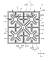
- FIG. 1 is a plan view schematically showing a light emitting element according to an embodiment of the present disclosure.
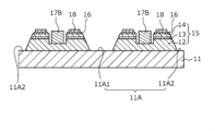
- 2 is an end view taken along the line II-II in FIG. 1.
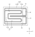
- FIG. 3 is a plan view schematically showing a light emitting element according to another embodiment of the present disclosure.
- FIG. 7 is a plan view schematically showing a light emitting element according to still another embodiment of the present disclosure.
- FIG. 1 is a plan view schematically showing a light emitting device according to an embodiment of the present disclosure. 6 is a sectional view taken along the line VI-VI in FIG. 5.
- FIG. FIG. 2 is a cross-sectional view for explaining a manufacturing method of an embodiment of a light emitting device of the present disclosure.
- FIG. 2 is a cross-sectional view for explaining a manufacturing method of an embodiment of a light emitting device of the present disclosure.
- FIG. 2 is a cross-sectional view for explaining a manufacturing method of an embodiment of a light emitting device of the present disclosure.
- FIG. 2 is a cross-sectional view for explaining a manufacturing method of an embodiment of a light emitting device of the present disclosure.
- FIG. 2 is a cross-sectional view for explaining a manufacturing method of an embodiment of a light emitting device of the present disclosure.
- FIG. 2 is a cross-sectional view for explaining a manufacturing method of an embodiment of a light emitting device of the present disclosure.
- the drawings referred to in the following description schematically show the embodiments, so the scale, spacing, positional relationship, etc. of each member may be exaggerated, or illustration of some members may be omitted. be. Furthermore, in the plan view and its cross-sectional view, the scale and spacing of each member may not match.
- the same name and code basically indicate the same or homogeneous member or member having the same function, and detailed description may be omitted as appropriate.
- the first direction means a direction parallel to one side of the semiconductor structure 15, and is the direction indicated by arrow F.
- the second direction means a direction perpendicular to the first direction, and is the direction pointed by arrow S.
- a light emitting element in an embodiment of the present disclosure includes a substrate 11, an n-side semiconductor layer 12, an active layer 13 disposed on the substrate 11, and an n-side semiconductor layer 12 and an active layer 13 in order from the substrate 11 side.
- a p-electrode 16 disposed on the p-side semiconductor layer 14 and electrically connected to the p-side semiconductor layer 14;
- the n-electrode 17 is arranged and electrically connected to the n-side semiconductor layer 12 .
- the n-electrode 17 includes a base portion 17A and a plurality of extending portions 17B extending from the base portion 17A.
- the substrate 11 includes an exposed portion 11A exposed from the semiconductor structure 15.
- the exposed portion 11A includes a first exposed portion 11A1 located between two adjacent extension portions 17B, and a second exposed portion 11A2 located on the outer periphery of the substrate 11 and connected to the first exposed portion 11A1.
- the p-electrode 16 is arranged between the extended portion 17B and the first exposed portion 11A1 when viewed from above.
- the first exposed portion 11A1 is arranged as the exposed portion 11A of the substrate 11 between two adjacent extension portions 17B.
- the semiconductor structure 15 As a result, compared to a light emitting element in which the exposed portion 11A is arranged only on the outer periphery of the semiconductor structure 15, light emitted from the active layer 13 is prevented from being absorbed by the semiconductor structure 15, and the semiconductor It becomes possible to extract light from the side surfaces of the structure 15 more efficiently. As a result, the efficiency of extracting light from the light emitting element can be improved, and the light emitting element can have high brightness. Moreover, since the first exposed portion 11A1 and the second exposed portion 11A2 are connected, when the side surface of the semiconductor structure 15 is covered with the covering member 21, as described later, the side surface of the semiconductor structure 15 is The covering member 21 can be easily arranged. Therefore, the light emitted from the side surface of the semiconductor structure 15 can be efficiently reflected toward the light extraction surface side by the covering member 21, and the light extraction efficiency of the light emitting device can be further improved.
- the semiconductor structure 15 includes, in order from the substrate 11 side, an n-side semiconductor layer 12, an active layer 13, and a p-side semiconductor layer 14.
- the upper surface of the n-side semiconductor layer 12 has a region where the active layer 13 and the p-side semiconductor layer 14 are arranged, and a region where the active layer 13 and the p-side semiconductor layer 14 are not arranged.
- the upper surface of the n-side semiconductor layer 12 has a region exposed from the active layer 13 and the p-side semiconductor layer 14.
- the region where the upper surface of the n-side semiconductor layer 12 is exposed from the active layer 13 and the p-side semiconductor layer 14 in this manner is referred to as an n-layer exposed portion.
- the n-layer exposed portion is surrounded by the active layer 13 and the p-side semiconductor layer 14 in plan view.
- the n-electrode 17 is electrically connected to the n-side semiconductor layer 12 at the n-layer exposed portion.
- the shape, size, position, and number of the n-layer exposed portions can be appropriately set depending on the intended size, shape, electrode shape, etc. of the light emitting element.
- the shape of the n-layer exposed portion may be a circle, an ellipse, a polygon such as a triangle, a quadrangle, or a hexagon, or a combination of these shapes in a plan view.
- the n-layer exposed portions are preferably arranged, for example, in point symmetry with respect to the center of the substrate 11 or in line symmetry with respect to a bisector that bisects one side of the substrate 11.
- the area of the n-layer exposed portion is preferably, for example, 30% or less, 25% or less, 20% or less, or 15% or less of the total area of the semiconductor structure 15. By setting it as such a range, the area of the active layer 13 can be maintained and the brightness can be improved.
- Examples of the semiconductor structure 15 include various semiconductors such as III-V group compound semiconductors and II-VI group compound semiconductors. Specifically , nitride - based semiconductor materials such as In , InGaAlN, etc. can be used. For the film thickness, layer structure, composition, etc. of each layer, those known in the art can be used.
- the emission peak wavelength of the light emitting element may be any of visible light, ultraviolet light, and infrared light.
- the active layer 13 and the n-side semiconductor layer 12 preferably include a semiconductor layer made of AlGaN with an Al composition ratio of 30% or more.
- the peak wavelength of light emitted from the active layer 13 is 250 nm or more and 330 nm or less.
- the light emitting element 10 that emits ultraviolet light can be used, for example, for purposes such as sterilization and disinfection.
- planar external shape of the semiconductor structure 15 examples include polygons such as quadrangles and hexagons, circles, and ellipses. In plan view, the outer edge of the semiconductor structure 15 is located inside the outer edge of the substrate 11.
- Substrate 11 supports semiconductor structure 15 .
- the substrate 11 may be one on which a semiconductor layer included in the semiconductor structure 15 can be epitaxially grown.
- Examples of the material of the substrate 11 include insulating substrates such as sapphire (Al 2 O 3 ) and spinel (MgA1 2 O 4 ), and nitride-based semiconductor substrates such as AlN and GaN.
- a nitride semiconductor for the semiconductor structure 15 it is preferable to use a sapphire substrate with a C-plane as a growth surface. Further, it may have an off angle of approximately 0° or more and 10° or less with respect to the C-plane of the sapphire substrate.
- the substrate 11 may have a plurality of convex portions on the upper surface on which the semiconductor structure 15 is arranged.
- the planar shape of the substrate 11 may be, for example, a polygon such as a quadrangle or a hexagon, a circle or an ellipse, and preferably a rectangle, a hexagon, or a shape with rounded corners.
- the upper surface of the substrate 11 includes an exposed portion 11A exposed from the semiconductor structure 15.
- the exposed portion 11A includes a first exposed portion 11A1 located between two adjacent extension portions 17B, and a second exposed portion 11A2 exposed from the semiconductor structure 15 at the outer peripheral portion of the substrate 11.
- the second exposed portion 11A2 is an area where the substrate 11 is exposed between the outer edge of the semiconductor structure 15 and the outer edge of the substrate 11.
- the first exposed portion 11A1 is connected to the second exposed portion 11A2.
- the second exposed portion 11A2 may be disposed only on a part of the outer periphery of the substrate 11, and is preferably disposed so as to surround the semiconductor structure 15.
- first exposed portions 11A1 are arranged in one semiconductor structure 15, and it is more preferable that three or more first exposed portions 11A1 are arranged.
- first exposed parts 11A1 are connected to the second exposed part 11A2.
- the covering member 21 described later can be placed on the side surface of the semiconductor structure 15 where the first exposed portion 11A1 is adjacent to the second exposed portion 11A2.
- the light emitted from the side surface of the semiconductor structure 15 can be efficiently reflected by the covering member 21 toward the light extraction surface side, and the brightness of the light emitting element can be further improved.
- the exposed portion 11A has a second exposed portion 11A2 arranged on the outer periphery of the rectangular substrate 11, as shown in FIG.
- the exposed portion 11A includes a first exposed portion 11A1 that is connected to a second exposed portion 11A2.
- the first exposed portions 11A1 extend along the second direction S at three positions that equally divide each side of the substrate 11 parallel to the first direction F into four. Further, the first exposed portions 11A1 extend in the first direction F from three positions that equally divide each side of the substrate 11 parallel to the second direction S into four.
- the first exposed portion 11A1 that extends along the second direction S from a position that bisects each side parallel to the first direction F of the substrate 11 has a portion that extends along the first direction F.
- first exposed portion 11A1 extending along the first direction F from a position that bisects each side parallel to the second direction S of the substrate 11 has a portion extending along the second direction S. .
- Three first exposed portions 11A1 connected to the second exposed portion 11A2 are arranged on each side of the substrate 11, for a total of 12 first exposed portions 11A1.
- the length of the first exposed portion 11A1 is, for example, 5% or more and 45% or less of one side of the substrate 11.
- the exposed portion 11A shown in FIG. 1 is arranged in point symmetry with respect to the center of the substrate 11.
- the width in the second direction S of the first exposed portion 11A1 extending in the first direction F and the width in the first direction F of the first exposed portion 11A1 extending in the second direction S are, for example, 0.2% of one side of the substrate 11. More than 5% is mentioned.
- the width in the second direction S of the second exposed portion 11A2 extending in the first direction F and the width in the first direction F of the second exposed portion 11A2 extending in the second direction S are, for example, 0.5% of one side of the substrate 11. Examples include 10% or less.
- the widths of the plurality of first exposed portions 11A1 may all be the same or may be different. Furthermore, the widths of the plurality of second exposed portions 11A2 may all be the same or may be different.
- the shape, size, position, etc. of the exposed portion 11A can be appropriately set depending on the size, shape, electrode shape, etc. of the light emitting element. Further, the shape, size, position, etc. of the exposed portion 11A can be appropriately set depending on the size of the semiconductor structure 15, the required output of the light emitting element, the brightness, etc.
- the area of the exposed portion 11A is, for example, 30% or less, 25% or less, 20% or less, or 15% or less of the total area of the substrate 11. By setting it as such a range, the area of the active layer 13 can be maintained and the brightness can be improved.
- the area of the first exposed portion 11A1 is 0.5% or more and 10% or less of the total area of the substrate 11.
- the area of the second exposed portion 11A2 is, for example, 1% or more and 20% or less of the total area of the substrate 11. By setting it as such a range, the area of the active layer 13 in the light emitting element 10 can be maintained and the brightness can be improved.
- the number of semiconductor structures 15 disposed on the substrate 11 is one.
- the number of semiconductor structures 15 being one means that the semiconductor structures 15 are not separated due to the arrangement of the exposed portions 11A in plan view.
- At least one first exposed portion 11A1 is preferably arranged between at least two extending portions 17B, as described later, and all first exposed portions 11A1 are preferably arranged between any of the extending portions 17B. It is more preferable that With such an arrangement, it is possible to further suppress the bias in the current density distribution, and it is possible to suppress uneven brightness in the entire light emitting element.
- the two first exposed portions 11A1 are a second exposed portion 11A2 at a position of 1/3 of the length of one side of the rectangular substrate 11 along the second direction S, and a second exposed portion 11A2 at a position of 2/3 of the length of the side. , and extend in the first direction F, respectively.
- the length of the first exposed portion 11A1 is, for example, 30% or more and 80% or less of one side of the substrate 11.
- the exposed portion 11A shown in FIG. 3 is arranged in line symmetry with respect to a bisector line that bisects one side of the substrate 11 extending in the first direction F.
- the exposed portions 11A include one first exposed portion 11A1 extending in the first direction F, and a second It has an exposed portion 11A2.
- the first exposed portion 11A1 extends in the first direction F from the second exposed portion 11A2 located at the midpoint of one side of the rectangular substrate 11 along the second direction S.
- the length of the first exposed portion 11A1 is, for example, 40% or more and 80% or less of one side of the substrate 11.
- the exposed portion 11A shown in FIG. 4 is arranged in line symmetry with respect to a bisector line that bisects one side of the substrate 11 extending in the first direction F.
- the light emitting element used in the light emitting device of the embodiment of the present disclosure shown in FIG. It has a second exposed part 11A2 arranged on the outer periphery.
- the four first exposed portions 11A1 each extend toward the center of the substrate 11 from the second exposed portion 11A2 located at the midpoint of each side of the rectangular substrate 11.
- the length of the first exposed portion 11A1 is, for example, 5% or more and 45% or less of one side of the substrate 11.
- the exposed portion 11A shown in FIG. 5 is arranged point-symmetrically with respect to the center of the substrate 11. Note that the first exposed portion 11A1 shown in FIGS. 3, 4, and 5 has a portion that is perpendicular to the linear portion or intersects at an angle of 45° to 135° from the linear portion of the first exposed portion 11A1. It's okay to stay.
- the n-electrode 17 and the p-electrode 16 are arranged on the upper surface side of the semiconductor structure 15.
- the p-electrode 16 is placed on the p-side semiconductor layer 14 and is electrically connected to the p-side semiconductor layer 14 .
- the p-electrode 16 is arranged between the extended portion 17B and the first exposed portion 11A1 when viewed from above. It is preferable that the p-electrode 16 be disposed on substantially the entire upper surface of the p-side semiconductor layer 14. In a top view, the p-electrode 16 preferably surrounds the entire outer periphery of the first exposed portion 11A1.
- the width of the p-electrode 16 located between the extended portion 17B and the first exposed portion 11A1 is preferably 10 ⁇ m or more, and more preferably 30 ⁇ m or more and 200 ⁇ m or less. By having such a width of the p-electrode 16, current can be efficiently diffused into the p-side semiconductor layer 14.
- a p pad electrode 18 electrically connected to the p electrode 16 is arranged on the upper surface of the p electrode 16 .
- the p pad electrode 18 may be arranged on the entire upper surface of the p electrode 16 or may be arranged on a part of the upper surface of the p electrode 16.
- the n-electrode 17 is disposed on the n-layer exposed portion where the n-side semiconductor layer 12 is exposed from the active layer 13 and the p-side semiconductor layer 14, and is electrically connected to the n-side semiconductor layer 12.
- the n-electrode 17 includes a base portion 17A and a plurality of extending portions 17B extending from the base portion 17A.
- the shape, size, etc. of the base portion 17A can be appropriately set depending on the shape, size, etc. of the semiconductor structure 15, the first exposed portion 11A1, the second exposed portion 11A2, etc. of the substrate 11.
- the shape of the base 17A can be various shapes, such as a polygon and a polygon with rounded corners.
- the extending portions 17B extend in different directions from a plurality of different positions on the base portion 17A.
- the base 17A is located at the center of the semiconductor structure 15 in plan view.
- the extending portions 17B extend linearly from the base portion 17A toward the four corners of the substrate 11.
- Each of the extending portions 17B may have a shape having one linear portion, or may have a shape having one linear portion and a portion extending from one linear portion. You can.
- the stretching direction of the portion stretched from one linear portion is not limited to one direction, but may be two directions, or three or more directions. Further, the stretching direction of the portion stretched from one linear portion may be, for example, a direction inclined at 45° or more and 90° or less with respect to the one linear shape. In FIG.
- one extending portion 17B extending from the base 17A includes one linear portion and one extending portion 17B extending from the one linear portion in two directions orthogonal to the one linear portion. It has a part. Such extending portions 17B extend from four positions of the base portion 17A.
- the n-electrode 17 shown in FIG. 1 is arranged point-symmetrically with respect to the center of the substrate 11.
- the n-electrode 17 has a base 17A located adjacent to one side extending in the second direction S.
- the n-electrode 17 has a plurality of extending portions 17B extending linearly in the first direction F from the base portion 17A.
- the extending portions 17B may each have a shape having one linear portion, or may have a shape having one linear portion and a portion extending from one linear portion. Good too.
- the three extending portions 17B may extend in parallel to each other from both ends and the center of the base portion 17A.
- the widths and lengths of the three extending portions 17B may be different from each other, but are preferably the same.
- the n-electrode 17 extends in the first direction F and is arranged in line symmetry with respect to a bisector line that bisects one side of the substrate 11.
- the n-electrode 17 has a base 17A located adjacent to one side extending in the second direction S.
- the n-electrode 17 has a plurality of extending portions 17B extending linearly in the first direction F from the base portion 17A.
- Each of the extending portions 17B may have a shape having one linear portion, or may have a shape having one linear portion and a portion extending from one linear portion. You can.
- the two extending portions 17B may extend parallel to each other from both ends of the base portion 17A.
- the widths and lengths of the two extending portions 17B may be different, but are preferably the same.
- the n-electrode 17 extends in the first direction F and is arranged in line symmetry with respect to a bisector line that bisects one side of the substrate 11.
- the first exposed portion 11A1 of the substrate 11 is disposed between at least two extending portions 17B, and all the first exposed portions 11A1 are , and is more preferably arranged between the extending portions 17B.
- the n-electrode 17, the p-electrode 16, and the p-pad electrode 18 are made of, for example, metals such as Au, Pt, Pd, Rh, Ru, Ni, W, Mo, Cr, Ti, Al, Cu, Ta, and Si, or alloys thereof. It can have a single layer structure or a laminated structure including. Specifically, the p-electrode 16 can have a laminated structure of Rh/Ni/Au, Ru/Ni/Au, or the like.
- the n-electrode 17 and the p-pad electrode 18 are made of Ti/Rh/Au, Ti/Pt/Au, W/Pt/Au, Rh/Pt/Au, which are laminated in order from the semiconductor structure 15 side.
- a laminated structure of Ni/Pt/Au, Ti/Ru/Ti, Ti/Al-Si/Ta/Ru, etc. can be used.
- Ti/Rh/Au" laminated in order from the semiconductor structure 15 side means that Ti, Rh, and Au are laminated in order from the semiconductor structure 15 side.
- the thickness of the n-electrode 17, the p-electrode 16, and the p-pad electrode 18 may be any of the thicknesses of films used in the field.
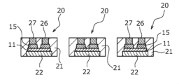
- a light emitting device 20 includes, for example, the above-described light emitting element 10 and a covering member 21, as shown in FIG. As shown in FIGS. 5 and 6, the light emitting device 20 has a p-side external connection portion 26 electrically connected to the p-electrode 16 and an n-side external connection portion 27 electrically connected to the n-electrode 17. are doing. A portion of the p-side external connection portion 26 and a portion of the n-side external connection portion 27 are exposed from the covering member 21. Such a configuration allows flip-chip mounting of the light emitting device 20. Further, in the light-emitting device 20, as shown in FIG. 7F, a light-transmitting member 22 may be disposed on the substrate 11 of the light-emitting element. In this case, it is preferable that the side surfaces of the substrate 11 and the side surfaces of the transparent member 22 are covered with the covering member 21.
- the covering member 21 covers at least the side surface of the n-side semiconductor layer 12 and the side surface of the active layer 13 adjacent to the exposed portion 11A.
- the covering member 21 preferably further covers the side surface of the p-side semiconductor layer 14 , and more preferably covers the side surface of the p-side external connection section 26 and the side surface of the n-side external connection section 27 .
- the light-transmitting member 22 is arranged in the light-emitting element 10, it is more preferable that the side surface of the light-transmitting member 22 is also covered with the covering member 21.
- coating refers not only to the state in which the covering member 21 is disposed in contact with the light emitting element 10 and/or the light-transmitting member 22, but also to the state in which the covering member 21 is disposed in contact with the light-emitting element 10 and/or the light-transmitting member 22. This includes a state in which the member 22 is disposed with another member, a space (for example, an air layer), etc. interposed therebetween. The upper surface of the translucent member 22 exposed from the covering member 21 becomes a light emitting surface of the light emitting device.
- the covering member 21 can be configured to include, for example, a translucent material and a light absorbing material and/or a reflective material contained therein.
- the light-transmitting material can be made of an organic material, an inorganic material, or the like.
- a resin containing a light-reflecting substance, a fluorescent material, a diffusing material, a coloring agent, etc. can be used. Any resin, light-reflective material, etc. that is commonly used in the field can be used.
- examples of the resin include resins or hybrid resins containing one or more of silicone resins, modified silicone resins, epoxy resins, modified epoxy resins, and acrylic resins.
- the light-reflective substance examples include silica, titanium oxide, zirconium oxide, potassium titanate, alumina, aluminum nitride, boron nitride, and mullite.
- the amount of light reflected, the amount of light transmitted, etc. can be varied depending on the content of the light-reflecting substance, etc. in the material constituting the covering member 21. It is preferable that the covering member 21 contains, for example, 20 wt% or more of a light-reflecting substance.
- the light-transmitting material is preferably an inorganic material, and more preferably the light-transmitting material and the light-reflecting substance are inorganic materials. That is, it is preferable that the main component of the covering member 21 is an inorganic material.
- the main component here means that it accounts for 50% or more of the total weight of the covering member.
- the covering member 21 is made of a plurality of inorganic materials.
- the covering member 21 may include a light reflective member and a support member that supports the light reflective member.
- the support member preferably contains silica and an alkali metal.
- the covering member 21 may further contain a scattering material.
- the covering member 21 is arranged on the first exposed portion 11A1 of the semiconductor structure 15, the light emitted from the semiconductor structure 15 near the first exposed portion 11A1 is more effectively reflected to the light extraction surface. be able to. Further, when the covering member 21 is made of only inorganic material, even if the light emitted from the light emitting device 20 is ultraviolet light, deterioration of the covering member 21 can be reduced, and the life of the light emitting device 20 can be reduced. It can be made longer.
- the light reflective member may be anything that can reflect light from the light emitting element 10, and examples thereof include ceramics such as boron nitride and alumina. It is preferable to use a plate-like or scale-like particulate material as the light-reflective member.
- the light reflective member may be either a primary particle or a secondary particle.
- the average particle diameter of the light reflective member is, for example, 0.1 ⁇ m or more and 100 ⁇ m or less, and preferably 0.6 ⁇ m or more and 43 ⁇ m or less.
- the average aspect ratio of the particles of the light reflective member is, for example, 10 or more, preferably 10 or more and 70 or less.
- the average aspect ratio is expressed as the ratio of the longest length passing through the center of one particle to the shortest length.
- the average particle size can be determined by cross-sectional observation using SEM, particle size distribution measurement using laser diffraction, and the like.
- the light reflective member having such an average particle size and average aspect ratio functions as an aggregate of the covering member 21 when the covering member 21 is heated by the heat generated from the light emitting element 10. Thereby, shrinkage of the covering member 21 due to the heat of the light emitting element 10 is suppressed, and a light emitting device with high heat resistance can be obtained. Such a light emitting device has a long service life. Further, the covering member 21 can reflect light from the light emitting element by utilizing the difference in refractive index between the light reflective member and the support member.
- the light emitting device can be used even under conditions where the heat generated from the light emitting element is large (for example, when a large amount of electric power is supplied to the light emitting element). becomes possible to use. Furthermore, by increasing the amount of power supplied to the light emitting element, the brightness per light emitting device can be increased.
- the support member is a member for supporting the light reflective member included in the covering member 21 and improving the strength of the covering member 21.
- the content ratio of the supporting member and the light reflective member included in the covering member 21 is, for example, 1:4 or more and 1:1 or less in terms of weight ratio. By setting it as this range, the shrinkage
- the average particle size of the silica is, for example, 0.1 ⁇ m or more and 10 ⁇ m or less. Within this range, the density per capacity of the light reflective member and the supporting member can be improved, and the strength of the covering member can be improved.
- the average particle size of the silica powder is preferably smaller than the average particle size of the light reflective member.
- the average particle size of the powder of the support member is a value measured before mixing with a solution containing an alkali metal.
- the alkali metal include potassium and sodium.
- the alkali metal is mixed with the silica in solution.
- Scattering materials include, for example, zirconia, titania, those surface-treated with silica, alumina, zirconia, zinc, organic substances, etc., stabilized zirconia or partially stabilized zirconia to which calcium, magnesium, yttrium, aluminum, etc. are added. Can be mentioned.
- zirconia As the scattering agent, which has low light absorption in the ultraviolet wavelength region.
- the scattering material preferably has an average particle size smaller than the average particle size of the light reflective member.
- the average particle size of the scattering material can be measured by laser diffraction.
- the linear thermal expansion coefficient of the covering member 21 is preferably 0.5 ppm/°C or more and 5 ppm/°C or less in the temperature range of 40°C to 300°C. Thereby, even if the temperature of the covering member 21 increases when the light emitting device is used, expansion of the covering member 21 can be suppressed.
- the p-side external connection portion 26 is electrically connected to the p-electrode 16
- the n-side external connection portion 27 is electrically connected to the n-electrode 17 .
- the p-side external connection section 26 and the n-side external connection section 27 are electrically connected to, for example, conductive wiring when the light emitting device 20 is mounted.
- the p-side external connection portion 26 and the n-side external connection portion 27 can be respectively arranged in a region obtained by dividing the area of the semiconductor structure 15 into two in a top view.
- the p-side external connection portion 26 and the n-side external connection portion 27 are arranged above the n-side semiconductor layer 12 and the p-side semiconductor layer 14, respectively, with the insulating film 25 interposed therebetween.
- the size, shape, etc. of the p-side external connection section 26 and the n-side external connection section 27 can be appropriately set depending on the intended performance of the light emitting device.
- metals such as Cu, Au, and Ni or alloys containing these metals can be used in a single-layer structure or a laminated structure.
- the thickness of the p-side external connection part 26 and the n-side external connection part 27 is, for example, 1 ⁇ m or more and 50 ⁇ m or less, preferably 10 ⁇ m or more and 30 ⁇ m or less.
- the insulating film 25 covers the top and side surfaces of the semiconductor structure 15 .
- the insulating film 25 has a p-side opening 25p above the p-electrode 16 in the region where the p-side external connection portion 26 is arranged, and has a p-side opening 25p above the p-electrode 16 in the region where the n-side external connection portion 27 is arranged. It has an n-side opening 25n above it.
- the n-side opening 25n is arranged in a region overlapping with the extension portion 17B of the n-electrode 17.
- the p-side external connection portion 26 is electrically connected to the p-electrode 16 through the p-side opening 25p.
- the n-side external connection portion 27 is electrically connected to the n-electrode 17 through the n-side opening 25n.
- the insulating film 25 covers the upper surface of the semiconductor structure 15 in this manner, the n-side external connection portion 27 can be placed on the upper surface of the insulating film 25 that covers the upper surface of the p-side semiconductor layer 14 .
- the p-side external connection portion 26 can be placed on the upper surface of the insulating film 25 that covers the upper surface of the n-side semiconductor layer 12 .
- the insulating film 25 is made of a material known in the art and has a material and thickness that is transparent and electrically insulating.
- the insulating film 25 is made of at least one kind of oxide or nitride selected from the group consisting of a metal oxide, a metal nitride, etc., for example, Si, Ti, Zr, Nb, Ta, and Al. be able to.
- the insulating film may have a thickness that allows light transmission and insulation.
- the light-emitting device has a light-transmitting member 22 on the substrate 11 of the light-emitting element 10.
- the light-transmitting member 22 is disposed to cover the light extraction surface of the light emitting element 10.
- the light-transmitting member 22 is a member that can transmit 50% or more, or 60% or more, preferably 70% or more, of the light emitted from the light emitting element 10 and emit it to the outside.
- the translucent member 22 can contain a phosphor capable of converting the wavelength of at least a portion of the light emitted from the light emitting element 10.
- the light-transmitting member 22 may contain a light-diffusing material that diffuses the light emitted from the light-emitting element 10.
- the light-transmitting member 22 is preferably plate-shaped, and the thickness of the light-transmitting member 22 is, for example, 50 ⁇ m or more and 300 ⁇ m or less.
- the translucent member 22 can be made of, for example, resin, glass, inorganic material, or the like.
- Examples of the light-transmitting member 22 containing phosphor include a sintered body of phosphor, resin, glass, or other inorganic material containing phosphor.
- a resin layer containing a phosphor may be formed on a flat molded body of resin, glass, inorganic material, or the like.
- the light-transmitting member 22 is made of an inorganic material, it has higher heat resistance than a light-transmitting member containing resin, so that a light-emitting device with high heat resistance can be manufactured.
- the translucent member 22 does not contain a wavelength conversion material, the light from the light emitting element is emitted to the outside without being wavelength converted.
- Examples of the phosphor to be contained in the translucent member 22 include yttrium-aluminum-garnet-based phosphor (e.g., Y 3 (Al, Ga) 5 O 12 :Ce), lutetium-aluminum-garnet-based phosphor (e.g., Lu 3 (Al, Ga) 5 O 12 :Ce), terbium-aluminum-garnet-based phosphors (e.g., Tb 3 (Al, Ga) 5 O 12 :Ce), CCA-based phosphors (e.g., Ca 10 (PO 4 ) 6 Cl 2 :Eu), SAE-based phosphor (e.g., Sr 4 Al 14 O 25 :Eu), chlorosilicate-based phosphor (e.g., Ca 8 MgSi 4 O 16 Cl 2 :Eu), oxynitride-based phosphor phosphors, nitride-based phosphors, fluoride-
- Examples of oxynitride-based phosphors include ⁇ -sialon-based phosphors (e.g., (Si,Al) 3 (O,N) 4 :Eu), ⁇ -sialon-based phosphors (e.g., Ca(Si,Al) 12 (
- Examples of nitride-based phosphors include SLA-based phosphors (e.g., SrLiAl 3 N 4 :Eu), CASN-based phosphors (e.g., CaAlSiN 3 :Eu), and SCASN-based phosphors .
- fluoride-based phosphors examples include KSF-based phosphors (e.g., K 2 SiF 6 :Mn), KSAF -based phosphors (e.g., Examples include K 2 Si 0.99 Al 0.01 F 5.99 :Mn) and MGF-based phosphors (for example, 3.5MgO.0.5MgF 2.GeO 2 :Mn).
- KSF-based phosphors e.g., K 2 SiF 6 :Mn
- KSAF -based phosphors examples include K 2 Si 0.99 Al 0.01 F 5.99 :Mn
- MGF-based phosphors for example, 3.5MgO.0.5MgF 2.GeO 2 :Mn.
- the translucent member 22 is arranged to cover the light extraction surface of the light emitting element 10.
- the light-transmitting member 22 and the light emitting element 10 may be joined through an adhesive or may be joined by a direct joining method.
- the adhesive for example, one using a translucent resin material such as epoxy resin or silicone resin can be used.
- a coating layer may be placed on the upper surface of the light-transmitting member 22 for the purpose of protecting the light-transmitting member 22, suppressing light reflection, or the like. Examples of the covering layer include an AR (Anti Reflection) layer.
- the light emitting device described above is Prepare the light emitting element 10, Prepare a sheet-like covering member 21A, A covering member 21A is arranged on the side of the substrate 11 on which the semiconductor structure 15 is arranged with respect to the light emitting element 10,
- the covering member 21A can be manufactured by forming the covering member 21A while applying vibration to the side surface of the semiconductor structure 15 of the light emitting element 10. It is preferable that the covering member 21 is placed on the side surface of the light emitting element 10 and then heated and cured.
- the curing is preferably performed in two stages: temporary curing and main curing. Thereby, generation of cracks in the formed covering member 21 can be suppressed.
- Temporary curing may be performed, for example, at a temperature of 80° C. or higher and 100° C. or lower for 10 minutes or more and 2 hours or less.
- the main curing may be performed, for example, at a temperature of 150° C. or more and 250° C. or less for 10 minutes or more and 3 hours or less.
- the pressure to be applied in this case is, for example, 0.5 MPa or more and 5 MPa or less, for example, 1 MPa.
- the applied pressure may be the same or different during temporary curing and main curing. Only one light-emitting element 10 may be prepared, or a plurality of light-emitting elements 10 may be prepared, a plurality of light-emitting devices may be formed at once, and the covering member 21A may be formed, and then the light-emitting devices 10 may be divided into individual light-emitting devices 20. Good too.
- a sheet-shaped covering member 21A is prepared.
- the sheet-like covering member 21A can be formed, for example, as follows.
- a mixture is prepared by mixing the light-reflecting member powder, the silica powder serving as the supporting member, and an alkaline solution.
- a scattering material may be mixed into this mixture.
- the mixture is mixed to a uniform viscosity, it is defoamed and stirred using a stirring/defoaming machine capable of stirring under reduced pressure. Thereafter, the mixture is applied onto a removable substrate 32 to form a sheet.
- FIG. 7B a plurality of light emitting elements 10 having translucent members 22 disposed on their upper surfaces are prepared.
- the translucent member 22 contains phosphor.
- the light-transmitting member 22 When bonding the light-transmitting member 22 and the light emitting element 10, a direct bonding method using surface activation bonding, atomic diffusion bonding, or hydroxyl group bonding may be used. It is preferable that the plurality of light emitting elements 10 be arranged at predetermined intervals and that the light-transmitting member 22 be attached to the adhesive sheet 31. Subsequently, as shown in FIG. 7C, the sheet-like covering member 21A is coated on the side where the p-side external connection portion 26 and the n-side external connection portion 27 of the light emitting element 10 are arranged, and the covering member is pressed. 21A is pushed in so as to be placed on the side surface of the light emitting element 10.
- the p-side external connection portion 26 and the n-side external connection portion 27 of the light emitting element 10 are covered with a covering member 21A.
- the covering member 21A can be easily placed on the side surface of the semiconductor structure 15 adjacent to the first exposed portion 11A1. Further, when forming the covering member 21A, by applying vibration while forming the covering member 21A, fluidity can be imparted to the covering member 21A, and the covering member 21A can be easily formed on the side surface of the light emitting element 10. Further, when forming the covering member 21A, forming the covering member 21A in a vacuum state can suppress the formation of a gap between the light emitting element 10 and the covering member 21A.
- the covering member 21A is ground to expose the upper surfaces of the p-side external connection portion 26 and the n-side external connection portion 27 from the covering member 21A. Subsequently, by cutting the covering member 21A located between the light emitting elements 10, the light emitting device 20 shown in FIG. 7F can be obtained.
- the covering member 21A can be cut using the blade 33, for example.
- the method for manufacturing a light emitting device described above it is possible to efficiently manufacture a light emitting device in which the efficiency of extracting light from the side surface of the semiconductor structure 15 adjacent to the first exposed portion 11A1 is improved.
- the covering member 21 can be easily placed on the side surface of the semiconductor structure 15.
- the light emitted from the side surface of the semiconductor structure 15 can be efficiently reflected toward the light extraction surface side, making it possible to obtain a light emitting device with further improved brightness.
- the n-electrode includes a base and a plurality of extending parts extending from the base,
- the substrate includes an exposed portion exposed from the semiconductor structure, In a top view, the exposed portion includes a first exposed portion located between two adjacent extension portions, and a second exposed portion located on the outer periphery of the substrate and connected to the first exposed portion.
- the p-electrode is a light emitting element disposed between the extended portion and the first exposed portion.
- the n-electrode includes three or more of the extending portions, 2.
- the light emitting element according to 1 or 2 above, wherein the second exposed portion surrounds the semiconductor structure when viewed from above. 4.
- 4. The light emitting device according to any one of 1 to 3 above, wherein the number of semiconductor structures is one. 5. 5. 5.
- the light emitting device according to any one of 1 to 4 above, wherein the active layer and the n-side semiconductor layer include a semiconductor layer made of AlGaN with an Al composition ratio of 30% or more. 6. 6. The light emitting device according to any one of 1 to 5 above, wherein the peak of the emission wavelength of light from the active layer is 250 nm or more and 330 nm or less. 7. The light emitting device according to any one of 1 to 6 above, A light emitting device including a covering member that covers at least a side surface of the n-side semiconductor layer and a side surface of the active layer adjacent to the exposed portion when viewed from above. 8. 8. The light emitting device according to 7 above, wherein the covering member has an inorganic material as a main component.
Landscapes
- Led Devices (AREA)
Priority Applications (3)
| Application Number | Priority Date | Filing Date | Title |
|---|---|---|---|
| CN202380035979.3A CN119156712A (zh) | 2022-04-26 | 2023-01-26 | 发光元件以及发光装置 |
| JP2024517839A JPWO2023210082A1 (https=) | 2022-04-26 | 2023-01-26 | |
| US18/730,830 US20250113671A1 (en) | 2022-04-26 | 2023-01-26 | Light emitting element and light emitting device |
Applications Claiming Priority (2)
| Application Number | Priority Date | Filing Date | Title |
|---|---|---|---|
| JP2022072564 | 2022-04-26 | ||
| JP2022-072564 | 2022-04-26 |
Publications (1)
| Publication Number | Publication Date |
|---|---|
| WO2023210082A1 true WO2023210082A1 (ja) | 2023-11-02 |
Family
ID=88518310
Family Applications (1)
| Application Number | Title | Priority Date | Filing Date |
|---|---|---|---|
| PCT/JP2023/002511 Ceased WO2023210082A1 (ja) | 2022-04-26 | 2023-01-26 | 発光素子及び発光装置 |
Country Status (4)
| Country | Link |
|---|---|
| US (1) | US20250113671A1 (https=) |
| JP (1) | JPWO2023210082A1 (https=) |
| CN (1) | CN119156712A (https=) |
| WO (1) | WO2023210082A1 (https=) |
Citations (12)
| Publication number | Priority date | Publication date | Assignee | Title |
|---|---|---|---|---|
| WO2004013916A1 (ja) * | 2002-08-01 | 2004-02-12 | Nichia Corporation | 半導体発光素子及びその製造方法並びにそれを用いた発光装置 |
| JP2006005215A (ja) * | 2004-06-18 | 2006-01-05 | Stanley Electric Co Ltd | 半導体発光素子及びその製造方法 |
| JP2006128457A (ja) * | 2004-10-29 | 2006-05-18 | Toyoda Gosei Co Ltd | 発光素子および発光装置 |
| JP2009043934A (ja) * | 2007-08-08 | 2009-02-26 | Toyoda Gosei Co Ltd | フリップチップ型発光素子 |
| JP2014225628A (ja) * | 2013-01-30 | 2014-12-04 | 日亜化学工業株式会社 | 半導体発光素子 |
| US20150076536A1 (en) * | 2013-08-27 | 2015-03-19 | Epistar Corporation | Light-emitting element having a plurality of light-emitting structures |
| JP2015153928A (ja) * | 2014-02-17 | 2015-08-24 | 日亜化学工業株式会社 | 半導体発光素子 |
| JP2016025341A (ja) * | 2014-07-25 | 2016-02-08 | 日亜化学工業株式会社 | 半導体発光素子 |
| JP2016528728A (ja) * | 2013-07-18 | 2016-09-15 | コーニンクレッカ フィリップス エヌ ヴェKoninklijke Philips N.V. | 高反射フリップチップledダイ |
| JP2017195370A (ja) * | 2016-04-18 | 2017-10-26 | ソウル バイオシス カンパニー リミテッドSeoul Viosys Co.,Ltd. | 高効率発光ダイオード |
| JP2018152564A (ja) * | 2017-03-14 | 2018-09-27 | ソウル バイオシス カンパニー リミテッドSeoul Viosys Co.,Ltd. | 発光ダイオード |
| US20190296204A1 (en) * | 2016-12-21 | 2019-09-26 | Seoul Viosys Co., Ltd. | Highly reliable light emitting diode |
-
2023
- 2023-01-26 JP JP2024517839A patent/JPWO2023210082A1/ja active Pending
- 2023-01-26 CN CN202380035979.3A patent/CN119156712A/zh active Pending
- 2023-01-26 US US18/730,830 patent/US20250113671A1/en active Pending
- 2023-01-26 WO PCT/JP2023/002511 patent/WO2023210082A1/ja not_active Ceased
Patent Citations (12)
| Publication number | Priority date | Publication date | Assignee | Title |
|---|---|---|---|---|
| WO2004013916A1 (ja) * | 2002-08-01 | 2004-02-12 | Nichia Corporation | 半導体発光素子及びその製造方法並びにそれを用いた発光装置 |
| JP2006005215A (ja) * | 2004-06-18 | 2006-01-05 | Stanley Electric Co Ltd | 半導体発光素子及びその製造方法 |
| JP2006128457A (ja) * | 2004-10-29 | 2006-05-18 | Toyoda Gosei Co Ltd | 発光素子および発光装置 |
| JP2009043934A (ja) * | 2007-08-08 | 2009-02-26 | Toyoda Gosei Co Ltd | フリップチップ型発光素子 |
| JP2014225628A (ja) * | 2013-01-30 | 2014-12-04 | 日亜化学工業株式会社 | 半導体発光素子 |
| JP2016528728A (ja) * | 2013-07-18 | 2016-09-15 | コーニンクレッカ フィリップス エヌ ヴェKoninklijke Philips N.V. | 高反射フリップチップledダイ |
| US20150076536A1 (en) * | 2013-08-27 | 2015-03-19 | Epistar Corporation | Light-emitting element having a plurality of light-emitting structures |
| JP2015153928A (ja) * | 2014-02-17 | 2015-08-24 | 日亜化学工業株式会社 | 半導体発光素子 |
| JP2016025341A (ja) * | 2014-07-25 | 2016-02-08 | 日亜化学工業株式会社 | 半導体発光素子 |
| JP2017195370A (ja) * | 2016-04-18 | 2017-10-26 | ソウル バイオシス カンパニー リミテッドSeoul Viosys Co.,Ltd. | 高効率発光ダイオード |
| US20190296204A1 (en) * | 2016-12-21 | 2019-09-26 | Seoul Viosys Co., Ltd. | Highly reliable light emitting diode |
| JP2018152564A (ja) * | 2017-03-14 | 2018-09-27 | ソウル バイオシス カンパニー リミテッドSeoul Viosys Co.,Ltd. | 発光ダイオード |
Also Published As
| Publication number | Publication date |
|---|---|
| CN119156712A (zh) | 2024-12-17 |
| JPWO2023210082A1 (https=) | 2023-11-02 |
| US20250113671A1 (en) | 2025-04-03 |
Similar Documents
| Publication | Publication Date | Title |
|---|---|---|
| US20250344559A1 (en) | Light emitting apparatus and method for producing the same | |
| US10714663B2 (en) | Method of manufacturing light emitting device | |
| JP5689225B2 (ja) | 発光装置 | |
| JP5521325B2 (ja) | 発光装置及びその製造方法 | |
| JP5463901B2 (ja) | 発光装置 | |
| JP5650885B2 (ja) | 波長変換焼結体及びこれを用いた発光装置、並びに波長変換焼結体の製造方法 | |
| JP6015734B2 (ja) | 発光装置 | |
| JP2003234008A (ja) | 面発光装置 | |
| US11081624B2 (en) | Method of manufacturing light emitting device having light guiding member in groove | |
| JP5644967B2 (ja) | 発光装置及びその製造方法 | |
| JP6274240B2 (ja) | 発光装置 | |
| JP6068473B2 (ja) | 波長変換粒子、波長変換部材及び発光装置 | |
| WO2023210082A1 (ja) | 発光素子及び発光装置 | |
| JP7299537B2 (ja) | 発光装置 | |
| JP2023095356A (ja) | 発光装置 | |
| JP2016189488A (ja) | 発光装置 | |
| JP7545085B2 (ja) | 発光装置 | |
| JP2025100167A (ja) | 発光装置、発光装置の製造方法 | |
| WO2024071218A1 (ja) | 発光装置および発光装置の製造方法 | |
| JP2024049355A (ja) | 発光装置および発光装置の製造方法 | |
| CN121866870A (zh) | 发光装置以及发光装置的制造方法 |
Legal Events
| Date | Code | Title | Description |
|---|---|---|---|
| 121 | Ep: the epo has been informed by wipo that ep was designated in this application |
Ref document number: 23795830 Country of ref document: EP Kind code of ref document: A1 |
|
| ENP | Entry into the national phase |
Ref document number: 2024517839 Country of ref document: JP Kind code of ref document: A |
|
| WWE | Wipo information: entry into national phase |
Ref document number: 18730830 Country of ref document: US |
|
| WWE | Wipo information: entry into national phase |
Ref document number: 202380035979.3 Country of ref document: CN |
|
| NENP | Non-entry into the national phase |
Ref country code: DE |
|
| WWP | Wipo information: published in national office |
Ref document number: 18730830 Country of ref document: US |
|
| 122 | Ep: pct application non-entry in european phase |
Ref document number: 23795830 Country of ref document: EP Kind code of ref document: A1 |