WO2023204309A1 - セラミックス膜及びその製造方法、エミッタ、熱光起電力発電装置 - Google Patents
セラミックス膜及びその製造方法、エミッタ、熱光起電力発電装置 Download PDFInfo
- Publication number
- WO2023204309A1 WO2023204309A1 PCT/JP2023/015991 JP2023015991W WO2023204309A1 WO 2023204309 A1 WO2023204309 A1 WO 2023204309A1 JP 2023015991 W JP2023015991 W JP 2023015991W WO 2023204309 A1 WO2023204309 A1 WO 2023204309A1
- Authority
- WO
- WIPO (PCT)
- Prior art keywords
- ceramic film
- ceramic
- emitter
- density
- film according
- Prior art date
- Legal status (The legal status is an assumption and is not a legal conclusion. Google has not performed a legal analysis and makes no representation as to the accuracy of the status listed.)
- Ceased
Links
Images








Classifications
-
- H—ELECTRICITY
- H02—GENERATION; CONVERSION OR DISTRIBUTION OF ELECTRIC POWER
- H02S—GENERATION OF ELECTRIC POWER BY CONVERSION OF INFRARED RADIATION, VISIBLE LIGHT OR ULTRAVIOLET LIGHT, e.g. USING PHOTOVOLTAIC [PV] MODULES
- H02S10/00—PV power plants; Combinations of PV energy systems with other systems for the generation of electric power
- H02S10/30—Thermophotovoltaic systems
-
- C—CHEMISTRY; METALLURGY
- C23—COATING METALLIC MATERIAL; COATING MATERIAL WITH METALLIC MATERIAL; CHEMICAL SURFACE TREATMENT; DIFFUSION TREATMENT OF METALLIC MATERIAL; COATING BY VACUUM EVAPORATION, BY SPUTTERING, BY ION IMPLANTATION OR BY CHEMICAL VAPOUR DEPOSITION, IN GENERAL; INHIBITING CORROSION OF METALLIC MATERIAL OR INCRUSTATION IN GENERAL
- C23C—COATING METALLIC MATERIAL; COATING MATERIAL WITH METALLIC MATERIAL; SURFACE TREATMENT OF METALLIC MATERIAL BY DIFFUSION INTO THE SURFACE, BY CHEMICAL CONVERSION OR SUBSTITUTION; COATING BY VACUUM EVAPORATION, BY SPUTTERING, BY ION IMPLANTATION OR BY CHEMICAL VAPOUR DEPOSITION, IN GENERAL
- C23C24/00—Coating starting from inorganic powder
- C23C24/02—Coating starting from inorganic powder by application of pressure only
- C23C24/04—Impact or kinetic deposition of particles
-
- C—CHEMISTRY; METALLURGY
- C23—COATING METALLIC MATERIAL; COATING MATERIAL WITH METALLIC MATERIAL; CHEMICAL SURFACE TREATMENT; DIFFUSION TREATMENT OF METALLIC MATERIAL; COATING BY VACUUM EVAPORATION, BY SPUTTERING, BY ION IMPLANTATION OR BY CHEMICAL VAPOUR DEPOSITION, IN GENERAL; INHIBITING CORROSION OF METALLIC MATERIAL OR INCRUSTATION IN GENERAL
- C23C—COATING METALLIC MATERIAL; COATING MATERIAL WITH METALLIC MATERIAL; SURFACE TREATMENT OF METALLIC MATERIAL BY DIFFUSION INTO THE SURFACE, BY CHEMICAL CONVERSION OR SUBSTITUTION; COATING BY VACUUM EVAPORATION, BY SPUTTERING, BY ION IMPLANTATION OR BY CHEMICAL VAPOUR DEPOSITION, IN GENERAL
- C23C24/00—Coating starting from inorganic powder
- C23C24/08—Coating starting from inorganic powder by application of heat or pressure and heat
-
- F—MECHANICAL ENGINEERING; LIGHTING; HEATING; WEAPONS; BLASTING
- F23—COMBUSTION APPARATUS; COMBUSTION PROCESSES
- F23D—BURNERS
- F23D14/00—Burners for combustion of a gas, e.g. of a gas stored under pressure as a liquid
- F23D14/12—Radiant burners
-
- C—CHEMISTRY; METALLURGY
- C04—CEMENTS; CONCRETE; ARTIFICIAL STONE; CERAMICS; REFRACTORIES
- C04B—LIME, MAGNESIA; SLAG; CEMENTS; COMPOSITIONS THEREOF, e.g. MORTARS, CONCRETE OR LIKE BUILDING MATERIALS; ARTIFICIAL STONE; CERAMICS; REFRACTORIES; TREATMENT OF NATURAL STONE
- C04B2237/00—Aspects relating to ceramic laminates or to joining of ceramic articles with other articles by heating
- C04B2237/50—Processing aspects relating to ceramic laminates or to the joining of ceramic articles with other articles by heating
- C04B2237/70—Forming laminates or joined articles comprising layers of a specific, unusual thickness
- C04B2237/704—Forming laminates or joined articles comprising layers of a specific, unusual thickness of one or more of the ceramic layers or articles
-
- Y—GENERAL TAGGING OF NEW TECHNOLOGICAL DEVELOPMENTS; GENERAL TAGGING OF CROSS-SECTIONAL TECHNOLOGIES SPANNING OVER SEVERAL SECTIONS OF THE IPC; TECHNICAL SUBJECTS COVERED BY FORMER USPC CROSS-REFERENCE ART COLLECTIONS [XRACs] AND DIGESTS
- Y02—TECHNOLOGIES OR APPLICATIONS FOR MITIGATION OR ADAPTATION AGAINST CLIMATE CHANGE
- Y02E—REDUCTION OF GREENHOUSE GAS [GHG] EMISSIONS, RELATED TO ENERGY GENERATION, TRANSMISSION OR DISTRIBUTION
- Y02E10/00—Energy generation through renewable energy sources
- Y02E10/50—Photovoltaic [PV] energy
Definitions
- the present disclosure relates to a ceramic film, a method for manufacturing the same, an emitter, and a thermophotovoltaic power generation device.
- Thermo-Photo-Voltaic (TPV) power generation is a technology that converts thermal radiation into electricity using a photoelectric conversion cell, and high efficiency power generation can be expected by controlling the radiation spectrum.
- TPV power generation has a wide range of applications because it can utilize various heat sources, and is attracting attention as a power generation technology with a high energy density per weight.
- FIG. 14 shows the basic configuration of the TPV power generation device.
- the TPV power generation device 100 shown in FIG. 14 converts heat generated by a combustion device or heat generated by condensing sunlight into infrared rays in an emitter 101, and converts the emitted infrared light into photo-voltaic (Photo-Voltaic). PV)) enters the element 102 and converts it into electric power.
- a combustion device or heat generated by condensing sunlight into infrared rays in an emitter 101
- Photo-Voltaic Photo-Voltaic
- Patent Document 1 includes a polycrystalline body having a garnet structure with a composition of R 3 Al 5 O 12 or R 3 Ga 5 O 12 (R: rare earth element), and has a porosity of 20% or more and 40% inside the polycrystalline body.
- a ceramic emitter having the following pores is disclosed. Although the pores are connected, they include portions that are not linearly continuous. Good wavelength selectivity can be obtained by not including a portion where holes are linearly continuous from the heat supply surface to the radiation surface of the ceramic emitter.
- Non-Patent Document 1 and Non-Patent Document 2 report an example in which a ceramic film is applied as an emitter of a TPV power generation device.
- Non-Patent Document 1 describes an emitter in which an Er 1.5 Y 1.5 Al 5 O 12 ceramic film is formed on a MoSi 2 substrate by plasma spray coating.
- Non-Patent Document 2 describes an emitter in which an Er 3 Al 5 O 12 ceramic film is formed on a SiC substrate by a sol-gel method.
- the surface of the combustor of a fuel-burning TPV power generation device can be coated with a ceramic film as an emitter, it will be possible to efficiently transfer heat from the heat source to the emitter, and higher efficiency as a power generation device can be expected.
- a ceramic film As described above, there is a need for an emitter film formation technique that can be easily combined with various types of heat sources.
- ceramic films generally have strength-related problems such as destruction due to temperature changes and peeling from the base material.
- the ceramic film described in Non-Patent Document 1 is formed on a base material, it is dense and has the problem of transmitting radiation from the base material.
- the ceramic membrane described in Non-Patent Document 2 is porous, it is difficult to control the porosity using the sol-gel method, and the porosity is as large as 57%. Therefore, there is a problem in that the concentration of Er ions contained in the emitter for producing wavelength selective radiation becomes low, and the radiation intensity becomes low.
- ceramic emitters have the problem that when forming a film that matches the form of the heat source, it is difficult to obtain a desired emission spectrum due to problems with strength and difficulty in controlling porosity.
- An object of the present disclosure is to provide a ceramic film having sufficient strength and capable of obtaining a desired radiation spectrum, a method for manufacturing the same, an emitter, and a thermophotovoltaic power generation device.
- a ceramic film according to one embodiment is a ceramic film having pores formed on a base material, and includes a plurality of high-density regions larger than the average density of the entire ceramic film, and a plurality of high-density regions larger than the average density of the entire ceramic film. It also includes a plurality of small low-density regions.
- a method for manufacturing a ceramic film forms the ceramic film on a base material by a plasma-assisted aerosol deposition method.
- An emitter is made of the above ceramic film formed on the heat source, which converts heat from the heat source into infrared rays.
- thermophotovoltaic power generation device includes an emitter that converts heat from a heat source into infrared rays, and a photoelectric conversion cell that converts the infrared rays emitted from the emitter into electric power, and the emitter is configured to It consists of the above-mentioned ceramic film formed thereon.
- thermophotovoltaic power generation device it is possible to provide a ceramic film having sufficient strength and capable of obtaining a desired radiation spectrum, a method for manufacturing the same, an emitter, and a thermophotovoltaic power generation device.
- FIG. 1 is a schematic diagram showing the configuration of a thermophotovoltaic power generation device according to an embodiment.
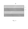
- FIG. 2 is a diagram illustrating an example of the structure of a ceramic film according to an embodiment.
- FIG. 7 is a diagram illustrating another example of the structure of the ceramic film according to the embodiment.
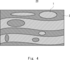
- FIG. 7 is a diagram illustrating another example of the structure of the ceramic film according to the embodiment.
- FIG. 2 is a schematic diagram illustrating a method for manufacturing a ceramic film according to an embodiment using a plasma-assisted aerosol deposition device.
- FIG. 2 is a schematic diagram illustrating a method for manufacturing a ceramic film according to an embodiment using a plasma-assisted aerosol deposition device.
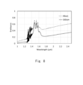
- FIG. 3 is a diagram showing an emissivity spectrum obtained by FT-IR measurement of thermal radiation from the Er 3 Ga 5 O 12 ceramic film formed on the ceramic film forming heater of Example 1.
- FIG. 3 is a SEM image showing a cross section of an Er 3 Ga 5 O 12 ceramic film formed on an Inconel substrate according to Example 2.
- 10 is an enlarged image of the ceramic film in FIG. 9 near the center in the thickness direction. This is an enlarged image obtained by further enlarging FIG. 10.
- 10 is an enlarged image of the vicinity of the surface of the ceramic film in FIG. 9.
- 10 is an enlarged image of the ceramic film in FIG. 9 near the substrate interface.
- FIG. 1 is a schematic diagram showing the basic configuration of a thermophotovoltaic power generation device.
- FIG. 1 is a schematic diagram showing a configuration example of a TPV power generation device 100 according to an embodiment.
- the TPV power generation device 100 includes an emitter 101A and a photoelectric conversion element 102.
- the emitter 101A converts heat from a heat source into thermal radiation (infrared light).
- the heat source is, for example, a combustion device that mixes and burns fuel and air to generate heat, and its mechanism and structure are not limited. Liquid fuel or gas may be used as the fuel. Further, the heat source may have a structure capable of supplying oxygen or the like instead of air. The converted infrared rays are emitted from the surface of the emitter 101A.
- the photoelectric conversion element 102 converts infrared rays emitted from the emitter 101A into electric power.
- the photoelectric conversion element 102 is sensitive to light in a specific wavelength band and has a wavelength band of light that can be photoelectrically converted. Therefore, it is desirable that the wavelength band of the infrared rays emitted from the emitter 101A coincides with the region in which the photoelectric conversion element 102 has high sensitivity.
- a silicon semiconductor, a compound semiconductor, or the like is used for the photoelectric conversion element 102.
- the power generated by the photoelectric conversion element 102 is collected through wiring (not shown).
- the emitter 101A is a wavelength selective heat radiator provided to cover the surface of the heat source.
- the emitter 101A selectively emits light of a specific wavelength to which the photoelectric conversion element 102 is sensitive. If the emitter 101A is made of a material that selectively emits light in a specific wavelength band to which the photoelectric conversion element 102 is sensitive, the power generation efficiency of the TPV power generation device 100 can be improved.
- FIG. 2 is a diagram showing an example of the structure of the ceramic film 20 according to the embodiment.
- This ceramic film 20 is formed on a base material (not shown) and has pores.
- the ceramic film 20 is formed on a heat source as a base material.
- the ceramic film 20 has a plurality of high-density regions 1 that are larger than the average density of the entire ceramic film 20 and a plurality of low-density regions 1 that are smaller than the average density of the entire ceramic film 20 in the film of the same composition. density region 2.
- the porosity of the high-density region 1 is smaller than the average porosity of the entire ceramic film 20
- the porosity of the low-density region 2 is larger than the average porosity of the entire ceramic film 20.
- the size of each region is also not limited.
- the size of the particles forming the ceramic film 20 is generally about 0.1 ⁇ m to 5 ⁇ m. Since the high-density region 1 and the low-density region 2 are composed of aggregates of particles, it is desirable that the size of each region is several ⁇ m or more.
- the thickness of the ceramic film 20 is not particularly limited, and can be, for example, 30 ⁇ m or more and 1 mm or less. Note that the upper limit of the size of each region is smaller than the thickness of the ceramic film 20.
- the low-density region 2 By providing a layer (low-density region 2) in which the porosity is larger than the average porosity in the ceramic film 20, even if there is thermal expansion or contraction during heating or cooling, the stress in the low-density region 2 is relaxed. This makes it possible to suppress the occurrence of peeling or destruction of the ceramic film 20.
- the thickness of the low-density region 2 is several ⁇ m or more. However, if the size of the low-density region 2 becomes too large, the mechanical strength of that portion will deteriorate, so it is desirable that the size is 20 ⁇ m or less, preferably 10 ⁇ m or less.
- the grain size of the ceramic in the low density region 2 is preferably 1 ⁇ m or less. The reason for this is that mechanical strength generally decreases in areas with large porosity, but by configuring this area with ceramic particles with a particle size of 1 ⁇ m or less and high surface energy, strength can be maintained. Because you will be able to do it.
- the average porosity of the ceramic membrane 20 is desirably 20% or more. Since the thermal radiation from the heat source irradiated onto the ceramic film 20 is scattered by the holes, the amount of thermal radiation transmitted through the ceramic film is suppressed. On the other hand, the infrared rays emitted from the ceramic film 20 have sufficient radiation intensity at the peak wavelength. As a result, wavelength-selective heat radiation by the ceramic film 20 is obtained.
- the average porosity of the ceramic membrane 20 is 40% or less. This is because it is thought that when the porosity of the ceramic film 20 increases, the ion concentration for producing wavelength selective radiation decreases, and the radiation intensity at the peak wavelength of infrared rays decreases.
- the porosity of the ceramic is 40% or more, the pores are connected to form a linear space, and the thermal radiation from the heat source is transmitted. This impairs the wavelength selectivity of the emitter 101A. Furthermore, if the porosity of the ceramic is 40% or more, the mechanical strength will be reduced, making it unsuitable for use as the emitter 101A of the TPV power generation device 100. Therefore, in order to suppress unnecessary thermal radiation from the heat source and obtain radiation intensity at a desired peak wavelength, the porosity is desirably 20% or more and 40% or less.
- the high-density region 1 and the low-density region 2 overlap in a layered manner.
- high-density regions 1 and low-density regions 2 of a constant thickness are alternately layered.
- the interface between each layer does not need to be smooth.
- the interface between the high-density region 1 and the low-density region 2 may be wave-shaped.
- the layer of one region may include the other region.
- a high-density region 1 and a low-density region 2 overlap in a layered manner, and the layer of the high-density region 1 includes a plurality of low-density regions 2 having elliptical cross sections and different sizes.
- the layer of the low-density region 2 includes a plurality of high-density regions 1 having elliptical cross sections and different sizes.
- the composition of the ceramic film 20 is not particularly limited. Since the ceramic film 20 is intended to be used as the photoelectric conversion element 102 of the TPV power generation device 100, it is desirable that the ceramic film 20 is made of oxide ceramics containing rare earth elements. More preferably, the composition of the ceramic film 20 is R 3 Ga 5 O 12 or R 3 Al 5 O 12 (R: rare earth element).
- FIGS. 5 and 6 are schematic diagrams illustrating a method for manufacturing a ceramic film according to an embodiment using the plasma-assisted aerosol deposition apparatus 200.
- the plasma-assisted aerosol deposition method is a method of forming a film by an aerosol deposition method (AD method) while using plasma-assisted energy.
- aerosol refers to fine particles of solid or liquid suspended in gas.
- the “AD method” is a film forming method in which an aerosol containing raw material powder is generated and the powder is deposited by injecting it from a nozzle toward a base material.
- FIG. 5 shows a part of the configuration of the plasma-assisted aerosol deposition device 200.
- the plasma-assisted aerosol deposition device 200 includes a nozzle 3 and a radio frequency (RF) coil 4 .
- a ceramic powder aerosol 5 is generated by blowing gas into a container (not shown) containing ceramic powder having the same composition as the ceramic film 20 to be formed. Ceramic powder aerosol 5 is injected from a nozzle 3 equipped with an RF coil 4 .
- the RF coil 4 is part of the plasma generator.
- the ceramic powder aerosol 5 is introduced into the RF coil 4 and turned into plasma to become a plasma section passing aerosol 6.
- the aerosol 6 passing through the plasma section collides with a base material 7 placed in a reduced pressure chamber (not shown), and a ceramic film 20 is formed on the base material 7 at room temperature.
- the gas for conveying the ceramic powder aerosol 5 and the plasma section passing aerosol 6 is not limited, for example, Ar or He can be used.
- the nozzle 3 can be of any shape, such as one with a circular discharge opening.
- the ceramic film 20 is formed over the entire surface of the base material 7 by moving a stage (not shown) on which the base material 7 is placed so that the center of the discharge port of the nozzle 3 scans over the base material 7 .
- the base material 7 may be fixed and a movable nozzle 3 may be used, or both the base material 7 and the nozzle 3 may be movable.
- the average porosity of the ceramic film 20 can be controlled by various film forming parameters (gas flow rate, chamber pressure, plasma power, stage movement speed, etc.). Further, a portion (high-density region 1) and a portion (low-density region 2) with a high porosity in the ceramic film 20 can be obtained, for example, by changing the above-mentioned film-forming parameters during film-forming.
- FIG. 6 shows the nozzle center locus 8 on the base material 7.
- the nozzle 3 advances from the upper left of the base material 7 in the +X direction, and then moves in the -Y direction by a predetermined step at the right end of the base material 7 and turns back. , proceed in the -X direction.
- a nozzle center locus 8 shown in FIG. 6 is obtained.
- the plasma section passing aerosol 6 injected from the nozzle 3 usually has a diameter of 10 mm or more, but the plasma intensity and particle concentration in the plasma section passing aerosol 6 have a spatial distribution. Therefore, the ceramic film 20 that is first attached to the base material 7 has a portion with high density and a portion with low density.
- the aerosol 6 passing through the plasma section moves and is sequentially deposited in such a state that there are high-density parts and low-density parts, high-density parts and low-density parts also occur in the thickness direction of the ceramic film 20. Furthermore, as shown by the nozzle center locus 8 in FIG. 6, during film formation, the nozzle 3 moves stepwise in the -Y direction by moving the base material 7. The distance of this step movement in the -Y direction is sufficiently smaller than the size of the plasma part passing aerosol 6 that is injected onto the base material 7. For this reason, it becomes possible to create a distribution of areas with higher porosity and areas with lower porosity.
- the ceramic film 20 having the same composition can be easily formed in a region (high density Region 1) and a small region (low density region 2) can be easily formed.
- Example 1 A specific example of the emitter 101A of the TPV power generation device 100 will be described below.
- Example 1 a film was formed by a plasma-assisted aerosol deposition method using as a raw material Er 3 Ga 5 O 12 powder synthesized by a solid phase reaction of an Er 2 O 3 powder reagent and a Ga 2 O 3 powder reagent and ground by a ball mill. The average particle size of the raw material powder is 0.7 ⁇ m.
- the film forming conditions were as follows: Ar gas flow rate 20 L/min, plasma output 2 kW, chamber pressure 105 Pa, X-direction stage movement speed 10 mm/sec, and Y-direction stage movement step 1 mm.
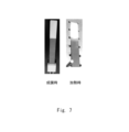
- FIG. 7 shows a photograph of the appearance of the ceramic film-forming heater (at the time of film formation) when a 40 ⁇ m thick ErGG ceramic film was formed on the silicon nitride heater, and the appearance when the ceramic film-forming heater was heated to approximately 1000°C. A photo (during heating) is shown.
- an ErGG ceramic film having a thickness of 160 ⁇ m was similarly formed on a silicon nitride heater, and the appearance when heated was observed, and almost no difference was observed in the appearance.
- FIG. 8 shows an emissivity spectrum obtained by FT-IR measurement of thermal radiation from the ErGG ceramic film formed on the silicon nitride heater of Example 1.
- FIG. 8 shows an emissivity spectrum measured by heating the surface temperature of the ErGG ceramic film to about 1000° C. using a silicon nitride heater. As shown in FIG. 8, wavelength-selective thermal radiation can be confirmed in both ErGG ceramic films with a thickness of 40 ⁇ m and a thickness of 160 ⁇ m.
- the ErGG ceramic film is selected as an emitter compatible with the GaSb photoelectric conversion element.
- the bandgap wavelength of GaSb is 1.7 ⁇ m, and the manufactured ErGG ceramic film exhibits wavelength selectivity suitable for that wavelength. Note that the ErGG ceramic film with a thickness of 160 ⁇ m exhibits higher wavelength selectivity than that with a thickness of 40 ⁇ m.
- Example 2 An ErGG ceramic film was formed on an Inconel alloy substrate as a base material under the same film forming conditions as in Example 1, and after cross-sectional processing by ion polishing, the results of SEM observation are shown in FIGS. 9 to 11.
- FIG. 9 is a low magnification SEM image. In FIG. 9, it can be seen that there are a high-density region 1, which is a region with a bright contrast with the Inconel alloy substrate 11, and a low-density region 2, a region with a dark contrast.
- FIG. 10 is an enlarged image of the ceramic film in FIG. 9 near the center in the thickness direction. It can be seen from FIG. 10 that the high-density region 1 and the low-density region 2 form a layer. The thickness of each layer is approximately 4 ⁇ m to 10 ⁇ m.
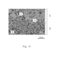
- FIG. 11 is a further enlarged image of FIG. 10. It can be seen that the low-density region 2 consists of particles with a particle size of 1 ⁇ m or less, and the high-density region 1 consists of particles with advanced particle sintering and a particle size of more than 1 ⁇ m. It is believed that these structures were obtained by forming a film while moving the substrate relative to the nozzle 3 using the plasma-assisted aerosol deposition apparatus 200. Further, when the porosity was calculated by image analysis of the SEM image shown in FIG. 11, the porosity was 40%.
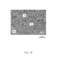
- FIG. 12 is an enlarged image of the vicinity of the surface of the ceramic film in FIG. 9. Further, FIG. 13 is an enlarged image of the ceramic film in FIG. 9 near the substrate interface.
- the porosity calculated by image analysis of these SEM images was 38% and 33%, respectively.
- the ceramic film 20 including the high-density region 1 and the low-density region 2 according to the embodiment has wavelength-selective thermal radiation suitable for the emitter 101A of the TPV power generation device 100 and has excellent heat resistance. This was confirmed. Moreover, it was also confirmed by SEM observation that the ceramic film 20 having the high-density region 1 and the low-density region 2 of the embodiment was obtained by a plasma-assisted aerosol deposition method. The high heat resistance of the ceramic film 20 of the embodiment can be considered to be due to the presence of the low density region 2 in the film.
- an emitter for TPV power generation that has excellent wavelength selectivity and is made of a ceramic film that does not peel or break from the base material even when heating and cooling cycles are applied. Furthermore, a method for manufacturing an emitter made of the above ceramic film can be provided.
Landscapes
- Chemical & Material Sciences (AREA)
- Engineering & Computer Science (AREA)
- Mechanical Engineering (AREA)
- Chemical Kinetics & Catalysis (AREA)
- Materials Engineering (AREA)
- Metallurgy (AREA)
- Organic Chemistry (AREA)
- Combustion & Propulsion (AREA)
- General Engineering & Computer Science (AREA)
- Other Surface Treatments For Metallic Materials (AREA)
- Photovoltaic Devices (AREA)
Abstract
Description
(実施例1)
実施例1では、Er2O3粉末試薬とGa2O3粉末試薬の固相反応により合成し、ボールミルにより粉砕したEr3Ga5O12粉末を原料としてプラズマ援用エアロゾルデポジション法により成膜した。原料粉末の平均粒径は0.7μmである。成膜条件は、Arガスを流量20L/min、プラズマ出力2kW、チャンバ圧力105Pa、X方向ステージ移動速度10mm/sec、Y方向ステージ移動ステップ1mmとした。
実施例1と同様の成膜条件で、基材としてのインコネル合金基板上にErGGセラミックス膜を成膜し、イオンポリッシングによる断面加工をした後、SEM観察した結果を図9から図11に示す。図9は低倍率のSEM像である。図9中には、インコネル合金基板11とコントラストが明るい部分である高密度領域1とコントラストが暗い部分である低密度領域2が存在することがわかる。
2 低密度領域
3 ノズル
4 RFコイル
5 セラミックス粉末エアロゾル
6 プラズマ部通過エアロゾル
7 基材
8 ノズル中心部軌跡
9 粒子
10 空孔
20 セラミックス膜
100 TPV発電装置
101 エミッタ
101A エミッタ
102 光電変換素子
200 プラズマ援用エアロゾルデポジション装置
Claims (9)
- 基材上に形成された空孔を有するセラミックス膜であって、
該セラミックス膜全体の平均密度よりも大きい複数の高密度領域と、
該セラミックス膜全体の平均密度よりも小さい複数の低密度領域と、
を含む、
セラミックス膜。 - 前記高密度領域と前記低密度領域とは層状に重なっている、
請求項1に記載のセラミックス膜。 - 前記セラミックス膜は、希土類元素を含む酸化物セラミックスからなる、
請求項1又は2に記載のセラミックス膜。 - 前記セラミックス膜に組成は、R3Ga5O12又はR3Al5O12(R:希土類元素)である、
請求項3に記載のセラミックス膜。 - 前記低密度領域のセラミックス粒子の粒径が1μm以下である、
請求項1又は2に記載のセラミックス膜。 - プラズマ援用エアロゾルデポジション法により、請求項1又は2に記載のセラミックス膜を基材上に形成する、
セラミックス膜の製造方法。 - 原料粉末を含むエアロゾルを噴出するノズルに対して、前記基材を相対的に移動させて、前記セラミックス膜を前記基材上に形成する、
請求項6に記載のセラミックス膜の製造方法。 - 熱源からの熱を赤外線に変換する、前記熱源上に形成された請求項1又は2に記載のセラミックス膜からなる、
エミッタ。 - 熱源からの熱を赤外線に変換するエミッタと、
前記エミッタから放射された前記赤外線を電力に変換する光電変換セルと、を備え、
前記エミッタは、前記熱源上に形成された請求項1又は2に記載のセラミックス膜からなる、
熱光起電力発電装置。
Priority Applications (1)
| Application Number | Priority Date | Filing Date | Title |
|---|---|---|---|
| US18/857,385 US20250286497A1 (en) | 2022-04-22 | 2023-04-21 | Ceramic film, method for manufacturing the same, emitter, and thermophotovoltaic power generation device |
Applications Claiming Priority (2)
| Application Number | Priority Date | Filing Date | Title |
|---|---|---|---|
| JP2022-070623 | 2022-04-22 | ||
| JP2022070623A JP7808252B2 (ja) | 2022-04-22 | 2022-04-22 | セラミックス膜及びその製造方法、エミッタ、熱光起電力発電装置 |
Publications (1)
| Publication Number | Publication Date |
|---|---|
| WO2023204309A1 true WO2023204309A1 (ja) | 2023-10-26 |
Family
ID=88419998
Family Applications (1)
| Application Number | Title | Priority Date | Filing Date |
|---|---|---|---|
| PCT/JP2023/015991 Ceased WO2023204309A1 (ja) | 2022-04-22 | 2023-04-21 | セラミックス膜及びその製造方法、エミッタ、熱光起電力発電装置 |
Country Status (3)
| Country | Link |
|---|---|
| US (1) | US20250286497A1 (ja) |
| JP (1) | JP7808252B2 (ja) |
| WO (1) | WO2023204309A1 (ja) |
Citations (6)
| Publication number | Priority date | Publication date | Assignee | Title |
|---|---|---|---|---|
| JPH11264059A (ja) * | 1997-11-18 | 1999-09-28 | United Technol Corp <Utc> | セラミック材料のコーティング及びコーティングを施す方法 |
| JP2014512160A (ja) * | 2011-04-06 | 2014-05-19 | コミッサリア ア レネルジー アトミーク エ オ ゼネルジ ザルタナテイヴ | 熱光起電力システムのためのエミッタ、及びそのようなエミッタを少なくとも一つ含む熱光起電力システム |
| WO2016042749A1 (ja) * | 2014-09-18 | 2016-03-24 | 日本電気株式会社 | セラミックエミッタ |
| JP2018090463A (ja) * | 2016-12-07 | 2018-06-14 | 日本電気株式会社 | 熱放射性セラミック、熱放射性セラミックの製造方法および熱光起電力発電装置 |
| CN109295451A (zh) * | 2018-10-12 | 2019-02-01 | 哈尔滨工业大学 | 等离子体辅助气溶胶沉积成膜方法及气溶胶沉积装置 |
| JP2020057522A (ja) * | 2018-10-02 | 2020-04-09 | トヨタ自動車株式会社 | 非水電解液二次電池用捲回電極体 |
-
2022
- 2022-04-22 JP JP2022070623A patent/JP7808252B2/ja active Active
-
2023
- 2023-04-21 US US18/857,385 patent/US20250286497A1/en active Pending
- 2023-04-21 WO PCT/JP2023/015991 patent/WO2023204309A1/ja not_active Ceased
Patent Citations (6)
| Publication number | Priority date | Publication date | Assignee | Title |
|---|---|---|---|---|
| JPH11264059A (ja) * | 1997-11-18 | 1999-09-28 | United Technol Corp <Utc> | セラミック材料のコーティング及びコーティングを施す方法 |
| JP2014512160A (ja) * | 2011-04-06 | 2014-05-19 | コミッサリア ア レネルジー アトミーク エ オ ゼネルジ ザルタナテイヴ | 熱光起電力システムのためのエミッタ、及びそのようなエミッタを少なくとも一つ含む熱光起電力システム |
| WO2016042749A1 (ja) * | 2014-09-18 | 2016-03-24 | 日本電気株式会社 | セラミックエミッタ |
| JP2018090463A (ja) * | 2016-12-07 | 2018-06-14 | 日本電気株式会社 | 熱放射性セラミック、熱放射性セラミックの製造方法および熱光起電力発電装置 |
| JP2020057522A (ja) * | 2018-10-02 | 2020-04-09 | トヨタ自動車株式会社 | 非水電解液二次電池用捲回電極体 |
| CN109295451A (zh) * | 2018-10-12 | 2019-02-01 | 哈尔滨工业大学 | 等离子体辅助气溶胶沉积成膜方法及气溶胶沉积装置 |
Also Published As
| Publication number | Publication date |
|---|---|
| JP2023160327A (ja) | 2023-11-02 |
| JP7808252B2 (ja) | 2026-01-29 |
| US20250286497A1 (en) | 2025-09-11 |
Similar Documents
| Publication | Publication Date | Title |
|---|---|---|
| US10371416B2 (en) | Spectrally selective coatings for optical surfaces | |
| JP4244549B2 (ja) | 光電変換素子及びその製造方法 | |
| US10544363B2 (en) | Ceramic emitter | |
| US20090316268A1 (en) | Quartz glass component with reflector layer and method for producing the same | |
| US20090017292A1 (en) | Reactive flow deposition and synthesis of inorganic foils | |
| KR101203963B1 (ko) | 광전 변환 소자 제조 장치 및 방법, 그리고 광전 변환 소자 | |
| CN109851377B (zh) | 一种激光诱导高温固相反应生成a2b2o7型热障涂层材料的方法 | |
| JP2009530818A (ja) | 薄シリコンまたはゲルマニウムシートおよび薄型シート製太陽電池 | |
| US10002982B2 (en) | Emitter for a thermo-photovoltaic system and thermo-photovoltaic system comprising at least one such emitter | |
| KR20120036817A (ko) | 인-시투 플라즈마/레이저 하이브리드 장치 및 방법 | |
| TW201203591A (en) | Hazy zinc oxide film for shaped CIGS/CIS solar cells | |
| JP2011503893A (ja) | アモルファスiii−v族半導体材料及びその製造方法 | |
| KR20170087380A (ko) | 마이크로웨이브를 이용한 탄화규소 섬유 발열체 및 이를 이용한 발열장치 | |
| KR20220015405A (ko) | 다중 구역 기능을 갖는 고온 알루미늄 질화물 히터 | |
| JP2017028268A (ja) | エッチングチャンバ部材としての、焼結ナノ結晶粒化イットリウムをベースとしたセラミックの使用 | |
| JPWO2016208174A1 (ja) | セラミックとその製造方法、エミッタおよび熱光起電力発電装置 | |
| JP7808252B2 (ja) | セラミックス膜及びその製造方法、エミッタ、熱光起電力発電装置 | |
| US6379789B1 (en) | Thermally-sprayed composite selective emitter | |
| KR101183021B1 (ko) | 내플라즈마 부재의 제조방법 | |
| KR102701152B1 (ko) | Euv 펠리클용 질화붕소 나노튜브 멤브레인의 제조장치 및 질화붕소 나노튜브 멤브레인을 포함하는 euv 펠리클 | |
| JP2011100879A (ja) | 化合物半導体薄膜及びその製造方法、並びに太陽電池 | |
| Bryan et al. | Inserting a low-refractive-index dielectric rear reflector into PERC cells: Challenges and opportunities | |
| WO2018100653A1 (ja) | セラミック及びその製造方法、並びに赤外線放射物品、エミッタ及び熱光起電力発電装置 | |
| KR101734472B1 (ko) | 마이크로웨이브를 이용한 탄화규소 섬유 발열체 및 이를 이용한 발열장치 | |
| CN116113534A (zh) | 用于生产结构的增材制造工艺 |
Legal Events
| Date | Code | Title | Description |
|---|---|---|---|
| 121 | Ep: the epo has been informed by wipo that ep was designated in this application |
Ref document number: 23791957 Country of ref document: EP Kind code of ref document: A1 |
|
| WWE | Wipo information: entry into national phase |
Ref document number: 18857385 Country of ref document: US |
|
| NENP | Non-entry into the national phase |
Ref country code: DE |
|
| 122 | Ep: pct application non-entry in european phase |
Ref document number: 23791957 Country of ref document: EP Kind code of ref document: A1 |
|
| WWP | Wipo information: published in national office |
Ref document number: 18857385 Country of ref document: US |