WO2023199883A1 - 電力増幅モジュール - Google Patents
電力増幅モジュール Download PDFInfo
- Publication number
- WO2023199883A1 WO2023199883A1 PCT/JP2023/014512 JP2023014512W WO2023199883A1 WO 2023199883 A1 WO2023199883 A1 WO 2023199883A1 JP 2023014512 W JP2023014512 W JP 2023014512W WO 2023199883 A1 WO2023199883 A1 WO 2023199883A1
- Authority
- WO
- WIPO (PCT)
- Prior art keywords
- transistor
- electrically connected
- circuit
- base
- emitter
- Prior art date
- Legal status (The legal status is an assumption and is not a legal conclusion. Google has not performed a legal analysis and makes no representation as to the accuracy of the status listed.)
- Ceased
Links
Images








Classifications
-
- H—ELECTRICITY
- H03—ELECTRONIC CIRCUITRY
- H03F—AMPLIFIERS
- H03F3/00—Amplifiers with only discharge tubes or only semiconductor devices as amplifying elements
- H03F3/20—Power amplifiers, e.g. Class B amplifiers, Class C amplifiers
- H03F3/24—Power amplifiers, e.g. Class B amplifiers, Class C amplifiers of transmitter output stages
- H03F3/245—Power amplifiers, e.g. Class B amplifiers, Class C amplifiers of transmitter output stages with semiconductor devices only
-
- H—ELECTRICITY
- H03—ELECTRONIC CIRCUITRY
- H03F—AMPLIFIERS
- H03F1/00—Details of amplifiers with only discharge tubes, only semiconductor devices or only unspecified devices as amplifying elements
- H03F1/02—Modifications of amplifiers to raise the efficiency, e.g. gliding Class A stages, use of an auxiliary oscillation
-
- H—ELECTRICITY
- H03—ELECTRONIC CIRCUITRY
- H03F—AMPLIFIERS
- H03F1/00—Details of amplifiers with only discharge tubes, only semiconductor devices or only unspecified devices as amplifying elements
- H03F1/02—Modifications of amplifiers to raise the efficiency, e.g. gliding Class A stages, use of an auxiliary oscillation
- H03F1/0205—Modifications of amplifiers to raise the efficiency, e.g. gliding Class A stages, use of an auxiliary oscillation in transistor amplifiers
- H03F1/0288—Modifications of amplifiers to raise the efficiency, e.g. gliding Class A stages, use of an auxiliary oscillation in transistor amplifiers using a main and one or several auxiliary peaking amplifiers whereby the load is connected to the main amplifier using an impedance inverter, e.g. Doherty amplifiers
-
- H—ELECTRICITY
- H03—ELECTRONIC CIRCUITRY
- H03F—AMPLIFIERS
- H03F1/00—Details of amplifiers with only discharge tubes, only semiconductor devices or only unspecified devices as amplifying elements
- H03F1/32—Modifications of amplifiers to reduce non-linear distortion
-
- H—ELECTRICITY
- H03—ELECTRONIC CIRCUITRY
- H03F—AMPLIFIERS
- H03F3/00—Amplifiers with only discharge tubes or only semiconductor devices as amplifying elements
- H03F3/189—High-frequency amplifiers, e.g. radio frequency amplifiers
- H03F3/19—High-frequency amplifiers, e.g. radio frequency amplifiers with semiconductor devices only
-
- H—ELECTRICITY
- H03—ELECTRONIC CIRCUITRY
- H03F—AMPLIFIERS
- H03F3/00—Amplifiers with only discharge tubes or only semiconductor devices as amplifying elements
- H03F3/20—Power amplifiers, e.g. Class B amplifiers, Class C amplifiers
- H03F3/21—Power amplifiers, e.g. Class B amplifiers, Class C amplifiers with semiconductor devices only
- H03F3/211—Power amplifiers, e.g. Class B amplifiers, Class C amplifiers with semiconductor devices only using a combination of several amplifiers
-
- H—ELECTRICITY
- H03—ELECTRONIC CIRCUITRY
- H03F—AMPLIFIERS
- H03F3/00—Amplifiers with only discharge tubes or only semiconductor devices as amplifying elements
- H03F3/20—Power amplifiers, e.g. Class B amplifiers, Class C amplifiers
- H03F3/24—Power amplifiers, e.g. Class B amplifiers, Class C amplifiers of transmitter output stages
-
- H—ELECTRICITY
- H03—ELECTRONIC CIRCUITRY
- H03F—AMPLIFIERS
- H03F2200/00—Indexing scheme relating to amplifiers
- H03F2200/451—Indexing scheme relating to amplifiers the amplifier being a radio frequency amplifier
Definitions
- the present disclosure relates to a power amplification module.
- the Doherty amplifier circuit is a highly efficient power amplifier.
- the Doherty amplifier circuit is configured by connecting in parallel a carrier amplifier that operates independently of the power level of an input signal and a peak amplifier that operates when the power level of the input signal is large. With this configuration, the Doherty amplifier circuit can improve efficiency compared to a normal power amplifier.
- the Doherty amplifier circuit described in Patent Document 1 includes a carrier amplifier that operates in class AB and a peak amplifier that operates in class C.
- a base bias current lower than the base bias current of the carrier amplifier is supplied to the peak amplifier.
- the operation is switched depending on the power level of the input signal, so the gain characteristics and phase characteristics for the output signal change when the peak amplifier starts operating. Therefore, there are problems in that the output signal is distorted, leakage power to adjacent channels is increased, and error vector amplitude is increased. This occurs because when the peak amplifier starts operating, the current flowing through the bias circuit that supplies the bias current to the peak amplifier is small, so that the peak amplifier cannot follow changes in the input signal.
- an object of the present disclosure is to provide a power amplification module including a Doherty amplifier circuit that improves the response delay of a bias circuit in a peak amplifier.
- a power amplification module includes a carrier amplification circuit, a carrier bias circuit that supplies a bias to the carrier amplification circuit, a peak amplification circuit, and a first transistor whose collector or drain is connected to a reference potential. and a peak bias circuit that supplies a bias from the emitter or source of the first transistor to the peak amplifier circuit, the peak bias circuit supplying a predetermined current from the emitter or source of the first transistor. It is electrically connected to a current output circuit that outputs.
- a power amplification module including a Doherty amplifier circuit that improves response delay of a bias circuit in a peak amplifier.
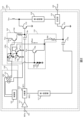
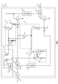
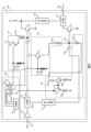
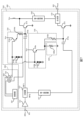
- FIG. 1 is a diagram showing an example of the configuration of a power amplification module according to a first embodiment. It is a figure showing an example of composition of a power amplification module concerning a 1st modification. It is a figure showing an example of the composition of the power amplification module concerning the 2nd modification. It is a figure showing an example of composition of a power amplification module concerning a 3rd modification. It is a figure showing an example of the composition of the power amplification module concerning a 2nd embodiment.
- FIG. 7 is a diagram illustrating an example of the relationship between a peak amplifier and a current output circuit when a plurality of peak amplifiers are configured in a power amplification module according to a second embodiment.
- FIG. 7 is a diagram showing an example of the relationship between a peak amplifier and a current output circuit when a plurality of peak amplifiers are configured in a power amplification module according to a third embodiment.
- FIG. 7 is a diagram showing another example of the relationship between the peak amplifier and the current output circuit in a case where the power amplification module according to the third embodiment includes a plurality of peak amplifiers.
- It is a figure showing an example of composition of a power amplification module concerning a 4th embodiment.
- FIG. 7 is a diagram showing an example of the relationship between a peak amplifier and a current output circuit when a plurality of peak amplifiers are configured in a power amplification module according to a third embodiment.
- FIG. 7 is a diagram showing another example of the relationship between the peak amplifier and the current output circuit in a case where the power amplification module according to the third embodiment includes a plurality of peak amplifiers
- FIG. 2 is a diagram showing an example of the configuration of a limiter circuit.
- FIG. 7 is a diagram showing another example of the configuration of the limiter circuit. It is a figure showing an example of the composition of the power amplification module concerning the 5th modification. It is a figure showing an example of composition of a power amplification module concerning a 5th embodiment. It is a figure showing an example of composition of a power amplification module concerning a 6th modification.
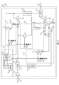
- FIG. 1 is a diagram showing a configuration example of various circuits related to a power amplification module 100 according to the first embodiment.
- the power amplification module 100 is mounted on, for example, a mobile phone and is used to amplify the power of a signal transmitted to a base station.
- the power amplification module 100 is, for example, 2G (second generation mobile communication system), 3G (third generation mobile communication system), 4G (fourth generation mobile communication system), 5G (fifth generation mobile communication system), LTE ( Long Term Evolution) - Signal power of communication standards such as FDD (Frequency Division Duplex), LTE-TDD (Time Division Duplex), LTE-Advanced, LTE-Advanced Pro, etc. can be amplified.
- the communication standards of the signals amplified by the power amplification module 100 are not limited to these.
- the power amplification module 100 includes, for example, a power amplification circuit 110, a current output circuit 120, and a current control circuit 130.
- the power amplifier circuit 110 is, for example, a Doherty amplifier circuit.
- the power amplification circuit 110 outputs a signal obtained by amplifying the input signal to a predetermined amplitude level.
- the power amplifier circuit 110 is a circuit that operates in a wide power range by varying the load impedance by the movement of the Doherty amplifier circuit.
- the current output circuit 120 supplies a constant current to the bias circuit of the peak amplifier in order to eliminate the fact that the bias circuit of the peak amplifier has a large output impedance.
- This is a circuit that controls the bias circuit.
- the current control circuit 130 is, for example, a circuit that supplies a constant current to the current output circuit 120.
- the power amplifier circuit 110 is shown to be configured with one carrier amplifier and one peak amplifier, but the present invention is not limited to this.
- the power amplifier circuit may include a plurality of carrier amplifiers and a plurality of peak amplifiers.
- the current output circuit 120 may be provided so as to cause a constant current to flow through the bias circuit of at least one of the plurality of peak amplifiers.
- the power amplifier circuit 110 includes, for example, a drive stage amplifier circuit 111, a distributor 112, a carrier amplifier 113, a carrier bias circuit 114, a peak amplifier 115, a peak bias circuit 116, and a 1 phase shifter 117 , a second phase shifter 118 , and a combining section 119 .
- Each component included in the power amplifier circuit 110 may be formed on the same substrate or on multiple substrates.
- the drive stage amplifier circuit 111 amplifies an input radio frequency (RF) signal RFin and outputs an amplified signal.
- the frequency of the signal RFin is, for example, about several GHz.
- the drive stage amplifier circuit 111 is, for example, a bipolar transistor such as a heterojunction bipolar transistor (HBT), or a metal-oxide-semiconductor field-effect transistor (MOSFET), but is not particularly limited. Consists of transistors such as Effect Transistor) be done. Note that the same applies to transistors that are a carrier amplifier 113 and a peak amplifier 115, which will be described later.
- the transistor will be described as a bipolar transistor.
- the transistor may be a field effect transistor (MOSFET).
- transistor is a field effect transistor, in the following, "current” will be replaced with “voltage”, “gate” will be replaced with “base”, “collector” will be replaced with “drain”, and “emitter” will be replaced with “source”.
- the distributor 112 divides, for example, the amplified signal output from the drive stage amplifier circuit 111 into a signal RF1 input to the carrier amplifier 113 and a signal RF2 input to the peak amplifier circuit 114.
- the signal RF2 passes through the first phase shifter 117 and is delayed by approximately 90 degrees in phase with respect to the phase of the signal RF1.
- the word "approximately 90 degrees delayed” includes delays of 45 degrees to 135 degrees.
- the distributor 112 may be, for example, a distributed constant circuit such as a coupled line 3 dB coupler or a Wilkinson type distributor.
- the carrier amplifier 113 for example, amplifies the signal RF1 input through the capacitor 113a and outputs an amplified signal.
- the carrier amplifier 113 is configured to include, for example, a transistor. Further, a load (not shown) is connected to the collector of the carrier amplifier 113, and when the peak amplifier 115 does not operate, the impedance becomes R, and when the peak amplifier operates (the peak amplifier saturates), the impedance becomes R/2. .
- Carrier amplifier 113 is biased to, for example, class A, class AB, or class B. That is, carrier amplifier 113 amplifies input signal RF1 and outputs an amplified signal without depending on the power level of the input signal.
- the carrier bias circuit 114 is, for example, a circuit that supplies a bias current to the base of the carrier amplifier 113.
- the carrier bias circuit 114 includes, for example, a transistor 114a, a diode 114b, a diode 114c, and a resistor 114d.
- the transistor 114a has a collector supplied with the power supply voltage Vcc, a base electrically connected to the current control circuit 130, and an emitter electrically connected to the base of the carrier amplifier 113 through a resistor 114d.
- the bias current supplied to the base of carrier amplifier 113 is output from the emitter of transistor 114a.
- Diode 114b and diode 114c are electrically connected in series, the anode of diode 114b is connected to the base of transistor 114a, and the cathode of diode 114c is connected to ground. Diode 114b and diode 114c set the base potential of transistor 114a. Note that the diode 114b and the diode 114c may be transistors whose bases and collectors are diode-connected.
- the peak amplifier 115 for example, amplifies the signal RF2 input through the capacitor 115a and outputs an amplified signal.
- the peak amplification circuit 115 includes, for example, a transistor.
- the peak amplifier 115 is, for example, class C biased. Note that the peak amplifier 115 may be biased to class A, class AB, or class B.
- the peak bias circuit 116 is, for example, a circuit that supplies a bias current to the base of the peak amplifier 115.
- the peak bias circuit 116 includes, for example, a transistor 116a, a diode 116b, a diode 116c, and a resistor 116d.
- the transistor 116a has a collector supplied with the power supply voltage Vcc, a base electrically connected to the current control circuit 130, and an emitter electrically connected to the base of the peak amplifier 115 through a resistor 116d.
- the bias current supplied to the base of peak amplifier 115 is output from the emitter of transistor 116a.
- Diode 116b and diode 116c are electrically connected in series, the anode of diode 116b is connected to the base of transistor 116a, and the cathode of diode 116c is connected to ground. Diode 116b and diode 116c set the base potential of transistor 116a.
- the first phase shifter 117 is connected to the base of the peak amplifier 115, for example.
- the first phase shifter 117 is, for example, a quarter wavelength line.
- the second phase shifter 118 is, for example, a quarter wavelength line electrically connected to the collector of the carrier amplifier 113. Thereby, the load impedance seen at the output end of the carrier amplifier 113 can be changed, and higher efficiency of the carrier amplifier 113 can be realized.
- the combining unit 119 combines the amplified signal output from the carrier amplifier 113 and output through the second phase shifter 118 with the amplified signal output from the peak amplifier 115, and outputs the output signal Pout to the output terminal 102.
- the current output circuit 120 controls the peak bias circuit 116 so that a current flows through the transistor 116a of the peak bias circuit 116, for example, when the peak amplifier 115 is not performing an amplifying operation.
- the current output circuit 120 includes, for example, a transistor 121, a transistor 122, a resistor 123, and a resistor 124.
- the transistor 121 is, for example, a transistor whose base and collector are diode-connected.
- the transistor 121 has a collector supplied with a reference current I 3 from a current control circuit 130, an emitter electrically connected to the ground (reference potential) through a resistor 123, and a base electrically connected to the base of the transistor 122. be done.
- the transistor 122 has a collector electrically connected to the emitter of the transistor 116a of the peak bias circuit 116, a base electrically connected to the base of the transistor 121, and an emitter electrically connected to the ground (reference potential) through the resistor 124. be done.
- the transistor 121 and the transistor 122 form a current mirror circuit.
- the current output circuit 120 controls the transistor 116a of the peak bias circuit 116 according to the reference current I3 supplied from the current control circuit 130 and the ratio between the resistance value of the resistor 123 and the resistance value of the resistor 124.
- a current I offset can be passed through the emitter. Therefore, the current output circuit 120 can cause current to flow through the transistor 116a when the peak amplifier 115 is not performing an amplification operation.
- the current output circuit 120 can lower the output impedance of the peak bias circuit 116 before the peak amplifier 115 performs the amplification operation, so that a delay in the response of the peak bias circuit 116 can be prevented.
- the current control circuit 130 is, for example, a circuit that supplies a constant reference current to the carrier bias circuit 114, the peak bias circuit 116, and the current output circuit 120.
- the current control circuit 130 includes, for example, a control section 131, a first current source 132, a second current source 133, and a third current source 134.
- the control unit 131 is, for example, a circuit that controls the current output from each of the first current source 132, the second current source 133, and the third current source 134.
- the first current source 132 is, for example, a current source for supplying the reference current I 1 to the carrier bias circuit 114.
- Carrier bias circuit 114 supplies a bias current to carrier amplifier 113 based on reference current I 1 .
- the second current source 133 is, for example, a terminal for supplying the reference current I 2 to the peak bias circuit 116.
- Peak bias circuit 116 supplies a bias current to peak amplifier 115 based on reference current I 2 .
- the third current source 134 is, for example, a terminal for supplying the reference current I 3 to the current output circuit 120.
- the current control circuit 130 supplies a constant current according to each of the carrier bias circuit 114, the peak bias circuit 116, and the current output circuit 120.
- the power amplification module 100 can supply appropriate currents to each of the carrier bias circuit 114, peak bias circuit 116, and current output circuit 120.
- An input signal RFin is input to the drive stage amplifier circuit 111 through the input terminal 101.
- the drive stage amplifier circuit 111 amplifies the input signal RFin and outputs an amplified signal.
- the amplified signal is distributed by a distributor 112 into a signal RF1 and a signal RF2.
- a signal RF1 is input to the carrier amplifier 113 through a capacitor 113a.
- a signal RF2 whose phase is delayed by 90 degrees by the first phase shifter 117 is input to the peak amplifier 115 through the capacitor 115a.
- the carrier bias circuit 114 supplies a bias current for class A, class AB, or class B operation to the carrier amplifier 113 through a resistor 114d.
- the base bias of the carrier bias circuit 114 is generated by supplying the reference current I 1 from the current control circuit 130 to the diode 114b and the diode 114c. That is, even when the power level of the input signal RFin is low, a current flows through the carrier amplifier 113, so a current also flows through the transistor 114a.
- the peak bias circuit 116 supplies a bias current for class C operation to the peak amplifier 115 through a resistor 116d.
- the base bias of the peak bias circuit 116 is generated by the reference current I 2 being supplied from the current control circuit 130 to the diode 116b and the diode 116c. That is, when the power level of the input signal RFin is low, no current flows through the peak amplifier 115, and therefore no current flows through the transistor 116a. As a result, the output impedance of the peak bias circuit 116 becomes high, and the time constant becomes slow, resulting in a problem that the amplitude envelope of the input signal RFin cannot be followed.
- the current output circuit 120 by providing the current output circuit 120, a constant current I offset is caused to flow through the transistor 116a of the peak bias circuit 116 regardless of the power level of the input signal RFin.
- the current output circuit 120 outputs (draws out) a constant current Ioffset from the emitter of the transistor 116a of the peak bias circuit 116, regardless of the power level of the input signal RFin. That is, when the power amplification module 100 is operating, the transistor 116a is always in the ON state regardless of the power level of the input signal RFin. In other words, even during a period in which no current is supplied to the peak amplifier 115 and it does not operate, current is supplied to the transistor 116a of the peak bias circuit 116. Thereby, in the power amplification module 100, even when the peak amplifier 115 starts operating, the output impedance of the peak bias circuit 116 can be lowered.
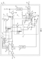
- FIG. 2 is a diagram showing an example of the configuration of a power amplification module 100a according to a first modification. For convenience, only the configurations different from the power amplification module 100 shown in FIG. 1 will be described below. In particular, similar effects due to similar configurations will not be mentioned sequentially.
- the power amplification module 100a uses a diode of the carrier bias circuit 114 to form a current output circuit 120a. Thereby, in the power amplification module 100a, the third output terminal 134 for supplying the reference current I 3 to the current output circuit 120 in the power amplification module 100 is unnecessary.
- the carrier bias circuit 114 includes a diode 114b and a diode 114c whose collectors and bases are diode-connected.
- the emitter of the diode 114c is electrically connected to ground through a resistor 125, and a transistor 126 is provided so as to form a current output circuit 120a.
- the transistor 126 has a base electrically connected to the base of the diode 114c, a collector electrically connected to the emitter of the transistor 116a, and an emitter electrically connected to ground through the resistor 127. That is, the transistor 126 forms a current mirror circuit with the diode 114c.
- the transistor 126 allows a constant current Ioffset to flow through the transistor 116a regardless of the power level of the input signal RFin.
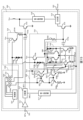
- FIG. 3 is a diagram showing an example of the configuration of a power amplification module 100b according to a second modification. For convenience, only the configurations different from the power amplification module 100 shown in FIG. 1 will be described below. In particular, similar effects due to similar configurations will not be mentioned sequentially.
- power amplification module 100b is configured to utilize diodes 114b and 114c of carrier bias circuit 114 in order to eliminate diodes 116b and 116c of peak bias circuit 116 in power amplification module 100. .
- the base bias diode of the peak bias circuit 116 can be reduced, and the second output terminal 133 for supplying the reference current I 2 to the peak bias circuit 116 becomes unnecessary.
- the transistor 116a of the peak bias circuit 116 has a base electrically connected to the base of the transistor 114a of the carrier bias circuit 114, a collector supplied with the power supply voltage Vcc, and an emitter connected to the peak amplifier 115 through a resistor 116d. electrically connected to the base of the That is, since the base potential of the peak amplifier 115 is set by the diodes 114b and 114c, the class C bias condition does not hold.
- the power amplification module 100b can operate the peak amplifier 115 in class C operation by connecting the current output circuit 120 to the emitter of the transistor 116a of the peak bias circuit 116 and extracting the current I offset from the emitter of the transistor 116a. .
- FIG. 4 is a diagram showing an example of the configuration of a power amplification module 100c according to a third modification. For convenience, only the configurations different from the power amplification module 100 shown in FIG. 1 will be described below. In particular, similar effects due to similar configurations will not be mentioned sequentially.
- the power amplification module 100c includes a current output circuit 120 and diodes 114b, 114c, 116b, and 116c for setting the base potentials of the carrier amplifier 113 and the peak amplifier 115. It has a combined current output circuit 120c.
- the current output circuit 120c controls the peak bias circuit 116 so that a current flows through the transistor 116a of the peak bias circuit 116, for example, when the peak amplifier 115 is not performing an amplification operation.
- the current output circuit 120c includes, for example, a transistor 121c, a transistor 122c, a transistor 123c, a resistor 124c, and a resistor 125c.
- the transistor 121c is, for example, a transistor whose base and collector are diode-connected.
- the transistor 121 has a collector supplied with the reference current I 1 from the current control circuit 130, a base electrically connected to the bases of the carrier amplifier 113 and the peak amplifier 115, and an emitter electrically connected to the emitter of the transistor 122c. Connected.
- the transistor 122c is, for example, a transistor whose base and collector are diode-connected.
- the emitter of the transistor 122c is electrically connected to the ground through the resistor 124c, and the base is electrically connected to the base of the transistor 123c.
- the base of the transistor 123c is electrically connected to the base of the transistor 122c, the collector is electrically connected to the emitter of the transistor 116a, and the emitter is electrically connected to ground through the resistor 125c.
- the current output circuit 120c sets the base potentials of the transistor 114a and the transistor 116a using a diode-connected transistor 121c and a transistor 122c. Further, the current output circuit 120c forms a current mirror circuit with a transistor 122c and a transistor 123c. Thereby, the current output circuit 120c can cause the current I offset to flow through the emitter of the transistor 116a of the peak bias circuit 116 in accordance with the reference current I 1 supplied from the current control circuit 130.
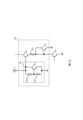
- FIG. 5 is a diagram showing an example of the configuration of a power amplification module 200 according to the second embodiment.
- FIG. 5 is a diagram showing an example of the configuration of a power amplification module 200 according to the second embodiment.
- FIG. 6 is a diagram showing an example of the relationship between the peak amplifier 215 and the current output circuit 220 when the power amplification module 200 according to the second embodiment includes a plurality of peak amplifiers 215.
- the second embodiment a description of common matters with the first embodiment will be omitted, and only different points will be explained. In particular, similar effects due to similar configurations will not be mentioned sequentially.
- the emitter of the transistor 216a of the peak bias circuit 216 is electrically connected to the base of the peak amplifier 215 through a resistor 216d. Note that one end of the resistor 216d is electrically connected to the emitter of the transistor 216a, and the other end of the resistor 216d is electrically connected to the node 215b that is electrically connected to the base of the peak amplifier 215.
- the current output circuit 220 includes, for example, a transistor 221, a transistor 222, a resistor 223, a resistor 224, and a resistor 225.
- the transistor 221, the resistor 223, and the resistor 224 are the same as the transistor 121, the resistor 123, and the resistor 124, respectively, so the description thereof will be omitted.
- the transistor 222 has a collector electrically connected to the node 215b through the resistor 225, a base electrically connected to the base of the transistor 221, and an emitter electrically connected to the ground through the resistor 224. That is, transistor 222 draws current I offset from the emitter of transistor 216a through resistor 225.
- the resistor 225 may be a resistor having a resistance value close to 0 ⁇ , or the current output circuit 220 may not include the resistor 225.
- a diode-connected bipolar transistor turns on at a voltage of approximately 1.3V. That is, the base potential of the transistor 216a becomes approximately 2.6V when the reference current I2 flows. Therefore, the emitter potential of transistor 216a is approximately 1.3V.
- the peak amplifier 215 turns on when the input signal RFin is small. Therefore, in order to properly operate the peak amplifier 215, the power amplification module 200 allows the current output circuit 220 to draw out the current I offset through the resistor 216d connected in series between the emitter of the transistor 216a and the node 215d. It is composed of Thereby, in the power amplification module 200, the peak amplifier 215 can be appropriately operated in class C by utilizing the voltage drop across the resistor 216d while flowing current through the transistor 216a.
- the power amplification module 200 includes a plurality of peak amplifiers 215.
- the power amplification module 200 is composed of a plurality of peak amplifiers 215.
- the peak amplifier 215 is not limited to being composed of three amplifiers, but may be composed of two or more amplifiers.
- Each of the plurality of peak amplifiers 215 is electrically connected in parallel. Specifically, the bases or gates of each of the plurality of peak amplifiers 215 and the collectors or drains of each of the peak amplifiers 215 are commonly connected.
- An input signal RF2 is input to the base of each of the plurality of peak amplifiers 215 through a capacitor 215a.
- the emitter of the transistor 216a is electrically connected to the base of each of the plurality of peak amplifiers 215 through a resistor 216d.
- each of the resistors 216d is electrically connected to the emitter of the transistor 216a, and the other end of each of the resistors 216d is electrically connected to a node 215b that is electrically connected to the base of each of the peak amplifiers 215. Ru.
- the collector of the transistor 222 of the current output circuit 220 is electrically connected to each of the nodes 215b through each of the resistors 225. That is, the transistor 222 draws the current I offset from the emitter of the transistor 216a through the resistor 216d and the resistor 225, respectively.
- the transistors constituting the peak amplifier are configured by a plurality of peak amplifiers 215, and the base bias from the transistor 216a is separately supplied to each of the plurality of peak amplifier circuits 215 via a separate resistor 216d. It is possible to suppress thermal runaway due to variations in the current drive capability of the In order to draw the current I offset from the emitter of the transistor 216a while maintaining the effect of suppressing thermal runaway, in this embodiment, the current I offset is not drawn directly from the emitter of the transistor 216a, but through each of the resistors 216d. A current Ioffset is extracted from the emitter of transistor 216a.
- the current I offset is extracted from the transistor 222 via the resistor 225 in addition to the resistor 216d. This has the effect of reducing interference received by the transistor 222 when an RF signal is applied to the base 215b of the transistor 215 via the capacitor 215a.
- the output impedance of the peak bias circuit 216 can be kept low even when current suddenly flows through the transistor of the peak amplifier.
- FIG. 7 is a diagram showing an example of the configuration of a power amplification module 300 according to the third embodiment.
- FIG. 8 is a diagram showing an example of the relationship between the peak amplifier 315 and the current output circuit 320 when the power amplification module 300 according to the third embodiment includes a plurality of peak amplifiers 215.
- FIG. 9 is a diagram showing another example of the relationship between the peak amplifier 315 and the current output circuit 320 when the power amplification module 300 according to the third embodiment includes a plurality of peak amplifiers 315.
- the third embodiment a description of common matters with the first embodiment will be omitted, and only different points will be explained. In particular, similar effects due to similar configurations will not be mentioned sequentially.
- the power amplification module 300 is configured such that a current output circuit 320 includes a resistor 320a.
- the resistor 320a has one end electrically connected to the emitter of the transistor 316a of the peak bias circuit 316, and the other end electrically connected to ground.
- Power amplification module 300 draws current Ioffset from the emitter of transistor 316a through resistor 320a.
- the power amplification module 300 can constantly supply current to the transistor 316a of the peak bias circuit 316 using a small number of elements.
- the power amplification module 300 includes a plurality of peak amplifiers 315.
- the power amplification module 300 is composed of a plurality of peak amplifiers 315.
- the peak amplifier 315 is not limited to being composed of three amplifiers, but may be composed of two or more amplifiers.
- Each of the plurality of peak amplifiers 315 is electrically connected in parallel.
- An input signal RF2 is input to the base of each of the plurality of peak amplifiers 315 through a capacitor 315a.
- the emitter of the transistor 316a is electrically connected to the base of each of the plurality of peak amplifiers 315 through each of the resistors 316d.
- each of the resistors 316d is electrically connected to the emitter of the transistor 316a, and the other end of each of the resistors 316d is electrically connected to each of the nodes 315b that are electrically connected to the respective bases of the peak amplifiers 315. Connected.
- each of the resistors 320a1, 320a2, and 320a3 is electrically connected to each of the nodes 315b, and the other end is electrically connected to the ground. That is, each of the plurality of resistors 320a draws a current Ioffset from the emitter of transistor 316a.
- the current of the transistors forming the peak amplifiers can be reduced. It is possible to suppress thermal runaway due to variations in driving ability.
- the current is applied to each of the resistors 216d.
- a resistor 320a forming an output circuit is connected to draw a current I offset from the emitter of the transistor 216a.
- the output impedance of the peak bias circuit 316 can be kept low even when current suddenly flows through the transistor of the peak amplifier.
- a deep class C bias can be applied to each of the plurality of peak amplifiers 315. Therefore, in the power amplification module 300, the peak amplifier can be operated only when the input signal is large, so that power consumption can be reduced.
- the power amplification module 300 includes a plurality of peak amplifiers 315
- the description of the common features with the embodiment shown in FIG. 8 will be omitted, and only the different points will be explained. In particular, similar effects due to similar configurations will not be mentioned sequentially.
- FIG. 10 is a diagram showing an example of the configuration of a power amplification module 400 according to the fourth embodiment.
- a description of common matters with the first embodiment will be omitted, and only different points will be explained. In particular, similar effects due to similar configurations will not be mentioned sequentially.
- the current output circuit 420 of the power amplification module 400 includes, for example, a transistor 421, a diode 422, a diode 423, a resistor 424, a resistor 425, a transistor 426, and a resistor 427.
- the transistor 421 has a base electrically connected to the current control circuit 430, a collector supplied with the power supply voltage Vcc, and an emitter electrically connected to the base of the transistor 426 through the resistor 425.
- the reference current I 3 is supplied to the base of the transistor 421 from the third output terminal 433 of the current control circuit 430.
- the diode 422, the diode 423, and the resistor 424, which are electrically connected in series, have one end electrically connected to the base of the transistor 421, and the other end electrically connected to the ground.
- the base potential of the transistor 421 is set by the diode 422, the diode 423, and the resistor 424.
- the transistor 426 has a base electrically connected to the emitter of the transistor 421, a collector electrically connected to the emitter of the transistor 416a of the peak bias circuit 416, and an emitter electrically connected to ground through the resistor 427. Further, an input signal RF2 is input to the base of the transistor 426 through a capacitor 428.
- a current I offset flows from the emitter of the transistor 416a to the collector of the transistor 426 in response to the reference current I3 input to the base of the transistor 421.
- a current ISB which is a self-bias current, flows from the emitter of the transistor 416a to the collector of the transistor 426 in response to the input signal RF2 input to the base of the transistor 426. That is, in the power amplification module 400, the current ISB increases as the power level of the input signal RF2 increases, so that the peak amplifier 415 can be suppressed from operating at a low input signal RF2.
- FIG. 11 is a diagram showing an example of the configuration of a power amplification module 400a according to a fourth modification.
- a description of common features with the power amplification module 400 shown in FIG. 10 will be omitted, and only different points will be described. In particular, similar effects due to similar configurations will not be mentioned sequentially.
- power amplification module 400a includes a limiter circuit 440.
- the limiter circuit 440 is, for example, a circuit for controlling the sum of the current Ioffset and the current ISB flowing through the collector of the transistor 426 so that it does not exceed a predetermined current value.
- Limiter circuit 440 is electrically connected in series between the emitter of transistor 416a and the collector of transistor 426, for example.
- FIG. 12 is a diagram showing an example of the configuration of the limiter circuit 440.
- FIG. 13 is a diagram showing another example of the configuration of the limiter circuit 440.
- the limiter circuit 440 includes, for example, a reference voltage circuit 441, a transistor 442, a resistor 443, and a transistor 444. Note that the limiter circuit 440 does not need to include the transistor 444.
- the reference voltage circuit 441 includes, for example, a transistor 441a, a resistor 441b, and a resistor 441c.
- the reference current I L is input to the collector of the transistor 441a, and the collector is electrically connected to the base of the transistor 442.
- the emitter of transistor 441a is electrically connected to ground.
- Resistor 441b electrically connects the base and collector of transistor 441a.
- Resistor 441c electrically connects the base and emitter of transistor 441a. That is, the reference voltage circuit 441 generates at the collector of the transistor 442 a voltage ⁇ V be that is ⁇ times the base-emitter voltage V be of the transistor 441a. " ⁇ times" is a multiple obtained by dividing the sum of the resistance value of the resistor 442b and the resistance value of the resistor 442c by the resistance value of the resistor 442c.
- the collector of the transistor 442 is electrically connected to the emitter of the transistor 416a, and the emitter is electrically connected to the collector of the transistor 426 through the resistor 443.
- the potential of the emitter of the transistor 442 is ( ⁇ -1)V be .
- the collector and base of the transistor 444 are electrically connected to the emitter of the transistor 442, and the emitter is electrically connected to ground.
- the transistor 444 operates as a protection circuit when the power level of the input signal RF2 increases.
- limiter circuit 440 has been described as being a different circuit from the current output circuit 420 in the above, this is only for convenience's sake. but not limited to.
- current output circuit 420 may be an integrated circuit including limiter circuit 440.
- the resistor 443 is connected between the reference voltage circuit 441 and the transistor 442, instead of being electrically connected in series between the emitter of the transistor 442 and the collector of the transistor 426. It is electrically connected in series with the base. In this case, when the collector current of transistor 426 increases, the base current of transistor 442 also increases. At this time, a potential difference occurs between both ends of the resistor 443. Then, the potential of the emitter of transistor 442 decreases, and the potential of the collector of transistor 426 decreases.
- FIG. 14 is a diagram showing an example of the configuration of a power amplification module 400b according to a fifth modification.
- FIG. 14 is a diagram showing an example of the configuration of a power amplification module 400b according to a fifth modification.
- a description of common matters with the power amplification module 400a according to the fourth modification shown in FIG. 11 will be omitted, and only different points will be described. In particular, similar effects due to similar configurations will not be mentioned sequentially.
- power amplification module 400b is configured to utilize a diode of carrier bias circuit 414 compared to power amplification module 400a. As a result, the number of diodes can be reduced, and the third output terminal 433 for supplying the reference current I 3 to the current output circuit 420 becomes unnecessary.
- the transistor 421 of the current output circuit 420 has a base electrically connected to the base of the transistor 414a of the carrier bias circuit 414, a collector connected to the power supply voltage Vcc, and an emitter connected to the base of the transistor 426 through the resistor 425. electrically connected to. That is, since the base potential of the transistor 421 is set by the diodes 414b and 414c, the transistor 421 operates under the same bias conditions as the carrier bias circuit 414.
- the emitter of the transistor 426 is electrically connected directly to the ground.
- the collector of the transistor 426 is electrically connected to the base of the peak amplifier 415 through the resistor 445, and the emitter of the transistor 416a is electrically connected to the collector of the transistor 426 indirectly through the resistor 445. It is set up so that In this way, the limiter circuit 440 can also be applied to the case where the current I offset is extracted from the emitter of the transistor 416a shown in the power amplification module 200 according to the second embodiment via the ballast resistor.
- FIG. 15 is a diagram showing an example of the configuration of a power amplification module 500 according to the fifth embodiment.
- a description of common features with the power amplification module 100 shown in FIG. 1 will be omitted, and only different points will be described. In particular, similar effects due to similar configurations will not be mentioned sequentially.
- the power amplification module 500 includes, for example, a current output circuit 520 and a limiter circuit 540.
- Current output circuit 520 includes, for example, transistors 521 to 527, resistors 528a to 528e, and capacitor 529.
- the transistor 521 is, for example, a transistor whose base and collector are diode-connected.
- the transistor 521 has a collector electrically connected to the emitter of the transistor 522, an emitter electrically connected to the ground through a resistor 528a, and a base electrically connected to the base of the transistor 523.
- the transistor 522 is, for example, a transistor whose base and collector are diode-connected.
- the transistor 522 has a collector electrically connected to the third output terminal 534 of the current control circuit 530, an emitter electrically connected to the collector of the transistor 521, and a base connected to the base of the transistor 524 and the base of the transistor 525. electrically connected.
- the transistor 523 has a collector electrically connected to the limiter circuit 540 and supplied with a current I offset , an emitter electrically connected to the ground through a resistor 528b, and a base electrically connected to the base of the transistor 521. be done.
- the collector of the transistor 524 is supplied with the power supply voltage Vcc, the emitter is electrically connected to the base of the transistor 526 through a resistor 528c, and the base is electrically connected to the base of the transistor 522.
- the collector of the transistor 525 is supplied with the power supply voltage Vcc, the emitter is electrically connected to the base of the transistor 527 through a resistor 528d, and the base is electrically connected to the base of the transistor 522.
- the transistor 526 has a collector electrically connected to the limiter circuit 540, an emitter electrically connected to ground (reference potential) through a resistor 528e, and a base electrically connected to the emitter of the transistor 524 through a resistor 528c. Ru.
- An input signal RF2 is input to the base of the transistor 526 through a capacitor 529.
- the transistor 527 has a collector electrically connected to the limiter circuit 540, an emitter electrically connected to the ground through a resistor 528f, and a base electrically connected to the emitter of the transistor 525 through a resistor 528d.
- the limiter circuit 540 includes, for example, transistors 541 and 542, resistors 543 and 545, and diodes 544 and 546. Note that the diodes 544 and 546 may be transistors whose bases and collectors are diode-connected.
- the collector of the transistor 541 is supplied with the power supply voltage Vcc, the emitter is electrically connected to the collector of the transistor 523, and the base is electrically connected to the collector of the transistor 526. Further, the emitter of the transistor 542 is electrically connected to the emitter of the transistor 542. Further, the transistor 541 has a collector electrically connected to the anode of the diode 544, and a base electrically connected to the cathode of the diode 544 through the resistor 543.
- the collector of the transistor 542 is electrically connected to the emitter of the transistor 516a, the emitter is electrically connected to the collector of the transistor 523, and the base is electrically connected to the collector of the transistor 527. Further, the emitter of the transistor 542 is electrically connected to the emitter of the transistor 541. Further, the base of the transistor 542 is electrically connected to the cathode of a diode 546 through a resistor 545. The anode of the diode 546 is supplied with the power supply voltage Vcc.
- the limiter circuit 540 is a differential pair circuit formed by a transistor 541 and a transistor 542.
- limiter circuit 540 does not need to include the diode 544 and the diode 546.
- the input signal RF2 is input to the base of the transistor 526 through the capacitor 529.
- a bias is supplied to the base of transistor 526 through transistor 524 and resistor 528c.
- a bias is supplied to the base of transistor 527 through transistor 525 and resistor 528d.
- the base potential of transistor 541 of limiter circuit 540 is determined by the collector current of transistor 526 and the characteristics of resistor 543 and diode 544.
- the base potential of transistor 542 of limiter circuit 540 is determined by the collector current of transistor 527 and the characteristics of resistor 545 and diode 546.
- the current flowing through the collector of transistor 526 increases, and the current flowing through the emitter of transistor 516a becomes equal to current Ioffset .
- the current I offset is controlled according to the base potentials of the differential pair of transistors 541 and 542.
- the increase in the diffusion capacitance between the base and collector of the transistor 426 is suppressed, and the increase in the collector potential of the transistor 426 is suppressed. Delays can be prevented. Therefore, the response speed of limiter circuit 540 becomes faster.
- the present invention is not limited to this.
- the present invention by adjusting the resistance value of the resistor 545 and the bias condition of the transistor 527, the current flowing through the transistor 516a when the peak amplifier 515 is not operating can be adjusted.
- FIG. 16 is a diagram illustrating an example of the configuration of a power amplification module 500a according to a sixth modification.
- a description of common features with the power amplification module 500 shown in FIG. 15 will be omitted, and only different points will be described. In particular, similar effects due to similar configurations will not be mentioned sequentially.
- the power amplification module 500a is configured such that the collector of the transistor 541 is electrically connected to the emitter of the transistor 516a, and the collector of the transistor 542 is supplied with the power supply voltage Vcc.
- a power amplification module 100 includes a carrier amplifier 113, a carrier bias circuit 114 that supplies a bias to the carrier amplifier 113, a peak amplifier 115, and a collector or drain connected to a reference potential.
- a peak bias circuit 116 that includes a transistor 116a (first transistor) and supplies a bias to the peak amplifier 115 from the emitter or source of the transistor 116a (first transistor); It is electrically connected to a current output circuit 120 that outputs a predetermined current from the emitter or source of (the first transistor).
- the power amplification module 100 improves the response delay of the bias circuit in the peak amplifier.
- the power amplification module 100 further includes a current output circuit 120. Thereby, the power amplification module 100 improves the response delay of the bias circuit in the peak amplifier.
- the reference current I 3 (first current) is supplied from the current control circuit 130 to the collector or drain, and the emitter or source is supplied with the reference current I 3 (first current) from the current control circuit 130.
- a transistor 121 (second transistor) is electrically connected to a reference potential and is diode-connected; a base or gate is electrically connected to the base or gate of the transistor 121 (second transistor), and a collector or drain is The transistor 122 (third transistor) is electrically connected to the emitter or source of the transistor 116a (first transistor), and the emitter or source is electrically connected to a reference potential.
- the power amplification module 100 can lower the output impedance of the peak bias circuit 116 before the peak amplifier 115 performs the amplification operation, thereby preventing a delay in the response of the peak bias circuit 116.
- the emitter or source of the transistor 121 (second transistor) of the power amplification module 100 is electrically connected to the reference potential through the resistor 123 (first resistor), and the transistor The emitter or source of 122 (third transistor) is electrically connected to the reference potential through resistor 124 (second resistor).
- the power amplification module 100 can lower the output impedance of the peak bias circuit 116 before the peak amplifier 115 performs the amplification operation, thereby preventing a delay in the response of the peak bias circuit 116.
- the emitter or source of the transistor 216a (first transistor) of the power amplification module 200 is the node 215b electrically connected to the input terminal of the peak amplifier 215,
- the collector or drain of the transistor 222 (third transistor) of the current output circuit 120 is electrically connected to the node 215b through the resistor 225 (fourth resistor). connected.
- the carrier bias circuit 114 of the power amplification module 100a includes a transistor 114a (fourth transistor) whose collector or drain is connected to a reference potential, and the current output circuit 120 includes: A reference current I 1 (first current) is supplied from the current control circuit 130 to the collector or drain of the transistor 114c (second transistor) through a diode-connected transistor 114b (fifth transistor), and the transistor 114a The base or gate of the transistor 114b (the fourth transistor) is electrically connected to the base or gate of the transistor 114b (the fifth transistor).
- the power amplification module 100a can be configured with a small circuit.
- the carrier bias circuit 114 of the power amplification module 100b has a collector or drain connected to a reference potential, and a base or gate connected to a reference current I 2 (first
- the current output circuit 120 includes a transistor 114a (fourth transistor) to which a reference current I 1 (second current) different from the reference current I 1 (second current) is supplied, and the current output circuit 120 has a base or gate of the transistor 116a (first transistor). It is electrically connected to the base or gate of the transistor 114a (fourth transistor).
- the power amplification module 100b can be configured with a small circuit.
- the carrier bias circuit 114 of the power amplification module 100c has a collector or drain connected to a reference potential, and a base or gate connected to a reference current I 1 (first a transistor 114a (fourth transistor) to which a current) is supplied, the base or gate of the transistor 114a (fourth transistor) is electrically connected to the base or gate of a transistor 116a (first transistor);
- the current output circuit 120 has an emitter or source electrically connected to the collector or drain of the transistor 122c (second transistor), and a reference current I 1 (first current) supplied from the current control circuit 130 to the collector or drain.
- the transistor further includes a diode-connected transistor 121c (fifth transistor) whose base or gate is electrically connected to the bases or gates of the transistor 114a (fourth transistor) and the transistor 116a (first transistor).
- a diode-connected transistor 121c (fifth transistor) whose base or gate is electrically connected to the bases or gates of the transistor 114a (fourth transistor) and the transistor 116a (first transistor).
- the current output circuit 320 of the power amplification module 300 has one end electrically connected to the emitter or source of the transistor 316a (first transistor), and the other end to the reference potential.
- a resistor 320a resistance element
- the power amplification module 300 can constantly supply current to the transistor 316a of the peak bias circuit 316 using a small number of elements.
- the peak amplifier 315 of the power amplification module 300 also includes a transistor 315 (sixth transistor) whose emitter or source is connected to the reference potential, and a resistor 320a of the current output circuit 320. The other end (of the resistive element) is electrically connected to the emitter or source of the transistor 315 (sixth transistor). This facilitates wiring for connecting each of the resistors 320a to the ground.
- the peak amplifier 415 of the power amplification module 400 includes a transistor 415 (sixth transistor) to which an input signal is input through a capacitor 415a (first capacitor) at the base or gate.
- the current output circuit 420 includes a transistor 421 (seventh transistor) whose collector or drain is connected to a reference potential and whose base or gate is supplied with current from the current control circuit 430, and a resistor 425 (seventh transistor) whose base or gate is connected to a reference potential.
- a transistor 426 (which is electrically connected to the emitter or source of the transistor 421 (seventh transistor) through the resistor 5), and whose collector or drain is electrically connected to the emitter or source of the transistor 416a (the first transistor);
- the base or gate of transistor 426 (eighth transistor) is connected to transistor 415 (sixth transistor) such that an input signal is input through capacitor 428 (second capacitor). electrically connected to the base or gate of the
- Power amplification module 400 also includes an electrical connection between the emitter or source of transistor 416a (first transistor) and the collector or drain of transistor 426 (eighth transistor).
- the circuit further includes a limiter circuit 440 that is connected in series with each other and limits the current flowing to the collector or drain of the transistor 426 (eighth transistor).
- the power amplification module 400 can suppress an increase in the current flowing through the collector of the transistor 442, and therefore can appropriately control the operation of the peak amplifier 415 even when the input signal RF2 becomes large.
- the carrier bias circuit 414 of the power amplification module 400b includes a transistor 414a (fourth transistor) whose base or gate is supplied with current from the current control circuit 430, and the transistor 421
- the base or gate of the transistor 414a (seventh transistor) is electrically connected to the base or gate of the transistor 414a (fourth transistor).
- the limiter circuit 440 of the power amplification module 400 has a base or gate electrically connected to a reference voltage circuit 441 (voltage setting circuit) for setting a reference voltage, and an emitter Alternatively, the transistor 442 (ninth transistor) whose source is electrically connected to the collector or drain of the transistor 426 (eighth transistor) through a resistor 443 (sixth resistor) is included.
- the power amplification module 400 can suppress an increase in the current flowing through the collector of the transistor 442, and therefore can appropriately control the operation of the peak amplifier 415 even when the input signal RF2 becomes large.
- the limiter circuit 440 of the power amplification module 400 has a base or gate connected to a reference voltage circuit 441 (voltage setting circuit) for setting a reference voltage, and a resistor 443 (sixth resistor). ), and includes a transistor 442 (ninth transistor) whose emitter or source is electrically connected to the collector or drain of transistor 426 (eighth transistor).
- the power amplification module 400 can suppress an increase in the current flowing through the collector of the transistor 442, and therefore can appropriately control the operation of the peak amplifier 415 even when the input signal RF2 becomes large.
- a power supply voltage is supplied to the collector or drain, and the collector or drain and the base or gate are electrically connected through the resistor 543 (seventh resistor).
- transistor 541 tenth transistor
- the current output circuit 520 further includes a limiter circuit 540 including a transistor 542 (eleventh transistor) to which the emitter or source is electrically connected to the emitter or source of the transistor 541 (the tenth transistor).
- the base or gate of the transistor 515 is the base or gate of the transistor 515 (sixth transistor) such that the base or gate is supplied with the reference current I3 from the current control circuit 530, and the input signal RF2 is input through the capacitor 529 (second capacitor).
- a transistor 526 (the twelfth transistor) whose collector or drain is electrically connected to the base or gate of the transistor 541 (the tenth transistor) and whose emitter or source is electrically connected to the reference potential ), the reference current I 3 is supplied from the current control circuit 530 to the base or gate, the collector or drain is electrically connected to the base or gate of the transistor 542 (the eleventh transistor), and the emitter or source is connected to the reference potential.
- a transistor 523 (third transistor) has a collector or drain electrically connected to the emitter or source of the transistor 542 (eleventh transistor). be done. Accordingly, in the power amplification module 500, the current I offset is controlled according to the base potentials of the differential pair of transistors 541 and 542, so that the response speed of the limiter circuit 540 becomes faster.
- the power amplification module 500a also has a collector or drain electrically connected to the emitter or source of the transistor 516a (first transistor), and a base or gate of the power amplification module 545 (seventh transistor).
- a transistor 541 (the tenth transistor) is supplied with a power supply voltage through a resistor (resistance of
- the current output circuit further includes a limiter circuit 540 including a transistor 542 (eleventh transistor) whose emitter or source is electrically connected to the emitter or source of the transistor 541 (the tenth transistor).
- the 520 is the base or gate of the transistor 515 (sixth transistor) such that the base or gate is supplied with the reference current I 3 from the current control circuit 130 and the input signal is input through the capacitor 529 (second capacitor).
- a transistor 526 (the twelfth transistor) whose collector or drain is electrically connected to the base or gate of the transistor 541 (the tenth transistor) and whose emitter or source is electrically connected to the reference potential ), the reference current I 3 is supplied from the current control circuit 530 to the base or gate, the collector or drain is electrically connected to the base or gate of the transistor 542 (the eleventh transistor), and the emitter or source is connected to the reference potential.
- a transistor 523 (third transistor) has a collector or drain electrically connected to the emitter or source of the transistor 541 (tenth transistor). be done. Thereby, the power amplification module 500a has a configuration that is effective when the peak amplifier 515 can secure a sufficiently large bias current due to the self-bias effect.
Landscapes
- Engineering & Computer Science (AREA)
- Power Engineering (AREA)
- Physics & Mathematics (AREA)
- Nonlinear Science (AREA)
- Amplifiers (AREA)
Abstract
キャリア増幅回路と、前記キャリア増幅回路にバイアスを供給するキャリアバイアス回路と、ピーク増幅回路と、コレクタまたはドレインが基準電位に接続される第1のトランジスタを含み、前記第1のトランジスタのエミッタまたはソースから、前記ピーク増幅回路にバイアスを供給するピークバイアス回路と、を備え、前記ピークバイアス回路は、前記第1のトランジスタのエミッタまたはソースから所定の電流を出力させる電流出力回路と電気的に接続される。
Description
本開示は、電力増幅モジュールに関する。
ドハティ増幅回路は、高効率な電力増幅器(パワーアンプ)である。ドハティ増幅回路は、入力信号の電力レベルに依存せず動作するキャリア増幅器と、入力信号の電力レベルが大きいときに動作するピーク増幅器とが並列に接続されて構成される。このように構成することによって、ドハティ増幅回路は、通常の電力増幅器に比べ効率を向上できる。
特許文献1に記載のドハティ増幅回路は、AB級で動作するキャリア増幅器と、C級で動作するピーク増幅器とを備える。当該ドハティ増幅回路では、キャリア増幅器のベースバイアス電流よりも低いベースバイアス電流をピーク増幅器に供給している。当該ドハティ増幅回路は、入力信号が大きくなると、ピーク増幅器が動作し始めることにより、キャリア増幅器の負荷を低くして大きな電力を出力する。このように、特許文献1に記載のドハティ増幅回路では、入力信号の電力レベルによって動作が切り替わるため、出力信号に対する利得特性および位相特性が、ピーク増幅器が動作し始めるときに変化する。このため、出力信号の歪みを発生させたり、隣接チャネルへの漏洩電力を増加させたり、エラーベクトル振幅を増加させたりするという問題があった。これは、ピーク増幅器が動作を開始するときに、ピーク増幅器にバイアス電流を供給するバイアス回路に流れる電流が小さいため、ピーク増幅器が入力信号の変化に追従できないために生じる。
そこで、本開示は、ピーク増幅器におけるバイアス回路の応答の遅延を改善するドハティ増幅回路を備える電力増幅モジュールを提供することを目的とする。
本発明の一側面に係る電力増幅モジュールは、キャリア増幅回路と、前記キャリア増幅回路にバイアスを供給するキャリアバイアス回路と、ピーク増幅回路と、コレクタまたはドレインが基準電位に接続される第1のトランジスタを含み、前記第1のトランジスタのエミッタまたはソースから、前記ピーク増幅回路にバイアスを供給するピークバイアス回路と、を備え、前記ピークバイアス回路は、前記第1のトランジスタのエミッタまたはソースから所定の電流を出力させる電流出力回路と電気的に接続される。
本開示によれば、ピーク増幅器におけるバイアス回路の応答の遅延を改善するドハティ増幅回路を備える電力増幅モジュールを提供することができる。
以下、各図を参照しながら本開示の各実施形態について説明する。ここで、同一符号の回路素子は、同一の回路素子を示すものとし、重複する説明を省略する。
===第1実施形態に係る電力増幅モジュール100===
図1は、第1実施形態に係る電力増幅モジュール100に関する各種回路の構成例を示す図である。電力増幅モジュール100は、例えば、携帯電話機に搭載され、基地局に送信する信号の電力を増幅するために用いられる。電力増幅モジュール100は、例えば、2G(第2世代移動通信システム)、3G(第3世代移動通信システム)、4G(第4世代移動通信システム)、5G(第5世代移動通信システム)、LTE(Long Term Evolution)-FDD(Frequency Division Duplex)、LTE-TDD(Time Division Duplex)、LTE-Advanced、LTE-Advanced Pro等の通信規格の信号の電力を増幅することができる。なお、電力増幅モジュール100が増幅する信号の通信規格はこれらに限られない。
===第1実施形態に係る電力増幅モジュール100===
図1は、第1実施形態に係る電力増幅モジュール100に関する各種回路の構成例を示す図である。電力増幅モジュール100は、例えば、携帯電話機に搭載され、基地局に送信する信号の電力を増幅するために用いられる。電力増幅モジュール100は、例えば、2G(第2世代移動通信システム)、3G(第3世代移動通信システム)、4G(第4世代移動通信システム)、5G(第5世代移動通信システム)、LTE(Long Term Evolution)-FDD(Frequency Division Duplex)、LTE-TDD(Time Division Duplex)、LTE-Advanced、LTE-Advanced Pro等の通信規格の信号の電力を増幅することができる。なお、電力増幅モジュール100が増幅する信号の通信規格はこれらに限られない。
電力増幅モジュール100は、例えば、電力増幅回路110、電流出力回路120および電流制御回路130を備える。
電力増幅回路110は、例えば、ドハティ増幅回路である。電力増幅回路110は、入力信号を所定の振幅レベルに増幅した信号を出力する。電力増幅回路110は、ドハティ増幅回路の動きによって、負荷インピーダンスを変動させて広い電力範囲で動作する回路である。
電流出力回路120は、例えば、ドハティ増幅回路のピーク増幅回路が動作するときに、ピーク増幅器のバイアス回路が大きい出力インピーダンスを有することを解消するために、ピーク増幅器のバイアス回路に一定の電流を流すよう当該バイアス回路を制御する回路である。
電流制御回路130は、例えば、電流出力回路120に一定の電流を供給する回路である。
なお、図1では、電力増幅回路110がキャリア増幅器とピーク増幅器がそれぞれ一つで構成されるように記載しているがこれに限定されない。複数のキャリア増幅器と複数のピーク増幅器とで構成される電力増幅回路であってもよい。この場合、複数のピーク増幅器のうち少なくともいずれかのピーク増幅器のバイアス回路に一定の電流を流すよう電流出力回路120が設けられていてもよい。
以下、電力増幅回路110、電流出力回路120および電流制御回路130の構成について説明する。
<<電力増幅回路110>>
図1に示すように、電力増幅回路110は、例えば、ドライブ段増幅回路111と、分配器112と、キャリア増幅器113と、キャリアバイアス回路114と、ピーク増幅器115と、ピークバイアス回路116と、第1移相器117と、第2移相器118と、合成部119とを含む。電力増幅回路110が備える各々の構成要素は、同一基板上に形成されてもよいし、複数の基板上に形成されてもよい。
<<電力増幅回路110>>
図1に示すように、電力増幅回路110は、例えば、ドライブ段増幅回路111と、分配器112と、キャリア増幅器113と、キャリアバイアス回路114と、ピーク増幅器115と、ピークバイアス回路116と、第1移相器117と、第2移相器118と、合成部119とを含む。電力増幅回路110が備える各々の構成要素は、同一基板上に形成されてもよいし、複数の基板上に形成されてもよい。
ドライブ段増幅回路111は、例えば、入力される無線周波数(RF:Radio-Frequency)信号RFinを増幅し、増幅信号を出力する。信号RFinの周波数は、例えば数GHz程度である。ドライブ段増幅回路111は、特に限定されないが、例えばヘテロ接合バイポーラトランジスタ(HBT:Heterojunction Bipolar Transistor)等のバイポーラトランジスタ、又は電界効果トランジスタ(MOSFET:Metal-oxide-semiconductor Field Effect Transistor)等のトランジスタにより構成される。なお、後述するキャリア増幅器113およびピーク増幅器115であるトランジスタについても同様である。
以下、一例として、トランジスタをバイポーラトランジスタとして説明する。ただし、トランジスタは電界効果トランジスタ(MOSFET:Metal-oxide-semiconductor Field Effect Transistor)でもよい。
トランジスタが電界効果トランジスタである場合、以下において、「電流」を「電圧」に、「ゲート」を「ベース」に、「コレクタ」を「ドレイン」に、「エミッタ」を「ソース」にそれぞれ読み替える。
分配器112は、例えば、ドライブ段増幅回路111から出力される増幅信号を、キャリア増幅器113に入力される信号RF1と、ピーク増幅回路114に入力される信号RF2とに分配する。ここで、信号RF2は、第1移相器117を通じて、信号RF1の位相に対して略90度遅れたものとなる。ここで「略90度遅れた」という単語には45度から135度遅れたものが含まれることとする。分配器112は、例えば、結合線路3dBカプラなどの分布定数回路やウィルキンソン型分配器であってもよい。
キャリア増幅器113は、例えば、キャパシタ113aを通じて入力される信号RF1を増幅して、増幅信号を出力する。キャリア増幅器113は、例えばトランジスタを含んで構成される。また、キャリア増幅器113のコレクタには、負荷(不図示)が接続され、ピーク増幅器115が動作しないときはインピーダンスRとなり、ピークアンプが動作する(ピークアンプが飽和する)とインピーダンスR/2となる。キャリア増幅器113は、例えば、A級、AB級またはB級にバイアスされる。すなわち、キャリア増幅器113は、入力信号の電力レベルに依存せず、入力信号RF1を増幅して、増幅信号を出力する。
キャリアバイアス回路114は、例えば、キャリア増幅器113のベースにバイアス電流を供給する回路である。キャリアバイアス回路114は、例えば、トランジスタ114a、ダイオード114b、ダイオード114c、抵抗114dを含む。トランジスタ114aは、コレクタには電源電圧Vccが供給され、ベースが電流制御回路130に電気的に接続され、エミッタが抵抗114dを通じてキャリア増幅器113のベースと電気的に接続される。キャリア増幅器113のベースに供給されるバイアス電流は、トランジスタ114aのエミッタから出力される。ダイオード114bとダイオード114cとは電気的に直列接続され、ダイオード114bのアノードがトランジスタ114aのベースに接続され、ダイオード114cのカソードがグランドに接続される。ダイオード114bおよびダイオード114cは、トランジスタ114aのベース電位を設定する。なお、ダイオード114bおよびダイオード114cは、ベースとコレクタとがダイオード接続されたトランジスタであってもよい。
ピーク増幅器115は、例えば、キャパシタ115aを通じて入力される信号RF2を増幅し、増幅信号を出力する。ピーク増幅回路115は、例えばトランジスタを含んで構成される。ピーク増幅器115は、例えばC級にバイアスされる。なお、ピーク増幅器115がA級、AB級、B級にバイアスされていてもよい。
ピークバイアス回路116は、例えば、ピーク増幅器115のベースにバイアス電流を供給する回路である。ピークバイアス回路116は、例えば、トランジスタ116a、ダイオード116b、ダイオード116c、抵抗116dを含む。トランジスタ116aは、コレクタには電源電圧Vccが供給され、ベースが電流制御回路130に電気的に接続され、エミッタが抵抗116dを通じてピーク増幅器115のベースと電気的に接続される。ピーク増幅器115のベースに供給されるバイアス電流は、トランジスタ116aのエミッタから出力される。ダイオード116bとダイオード116cとは電気的に直列接続され、ダイオード116bのアノードがトランジスタ116aのベースに接続され、ダイオード116cのカソードがグランドに接続される。ダイオード116bおよびダイオード116cは、トランジスタ116aのベース電位を設定する。
第1移相器117は、例えば、ピーク増幅器115のベースに接続される。第1移相器117は、例えば1/4波長線路である。
第2移相器118は、例えば、キャリア増幅器113のコレクタと電気的に接続される例えば1/4波長線路である。これにより、キャリア増幅器113の出力端で見た負荷インピーダンスを変化させて、キャリア増幅器113の高効率化を実現できる。
合成部119は、例えば、キャリア増幅器113から出力されて第2移相器118を通じて出力される増幅信号と、ピーク増幅器115から出力される増幅信号とを合成して、出力端子102に出力信号Poutを出力する。
<<電流出力回路120>>
電流出力回路120は、例えば、ピーク増幅器115が増幅動作していないときに、ピークバイアス回路116のトランジスタ116aに電流を流すように、ピークバイアス回路116を制御する。
<<電流出力回路120>>
電流出力回路120は、例えば、ピーク増幅器115が増幅動作していないときに、ピークバイアス回路116のトランジスタ116aに電流を流すように、ピークバイアス回路116を制御する。
電流出力回路120は、例えば、トランジスタ121と、トランジスタ122と、抵抗123と、抵抗124とを含む。
トランジスタ121は、例えば、ベースとコレクタとがダイオード接続されたトランジスタである。トランジスタ121は、例えば、コレクタには電流制御回路130から基準電流I3が供給され、エミッタが抵抗123を通じてグランド(基準電位)と電気的に接続され、ベースがトランジスタ122のベースと電気的に接続される。
トランジスタ122は、コレクタがピークバイアス回路116のトランジスタ116aのエミッタと電気的に接続され、ベースがトランジスタ121のベースと電気的に接続され、エミッタが抵抗124を通じてグランド(基準電位)と電気的に接続される。
すなわち、電流出力回路120は、トランジスタ121とトランジスタ122とでカレントミラー回路を形成する。これにより、電流出力回路120は、電流制御回路130から供給される基準電流I3と、抵抗123の抵抗値と抵抗124の抵抗値との比とに応じて、ピークバイアス回路116のトランジスタ116aのエミッタに電流Ioffsetを流すことができる。このため、電流出力回路120は、ピーク増幅器115が増幅動作をしていないときに、トランジスタ116aに電流を流すことができる。これにより、電流出力回路120は、ピーク増幅器115が増幅動作をする前に、ピークバイアス回路116の出力インピーダンスを低くできるため、ピークバイアス回路116の応答の遅延を防止できる。
なお、電流出力回路120は、抵抗123および抵抗124を含んでいなくてもよい。この場合、トランジスタ121、トランジスタ122及び基準電流I3を調整することによって、トランジスタ116aに所望の電流Ioffsetを流すことができる。
<<電流制御回路130>>
電流制御回路130は、例えば、キャリアバイアス回路114、ピークバイアス回路116及び電流出力回路120に一定の電流である基準電流を供給する回路である。
<<電流制御回路130>>
電流制御回路130は、例えば、キャリアバイアス回路114、ピークバイアス回路116及び電流出力回路120に一定の電流である基準電流を供給する回路である。
電流制御回路130は、例えば、制御部131と、第1電流源132と、第2電流源133と、第3電流源134とを含む。
制御部131は、例えば、第1電流源132、第2電流源133及び第3電流源134のそれぞれから出力される電流を制御する回路である。
第1電流源132は、例えば、キャリアバイアス回路114に基準電流I1を供給するための電流源である。キャリアバイアス回路114は、基準電流I1に基づきバイアス電流をキャリア増幅器113に供給する。
第2電流源133は、例えば、ピークバイアス回路116に基準電流I2を供給するための端子である。ピークバイアス回路116は、基準電流I2に基づきバイアス電流をピーク増幅器115に供給する。
第3電流源134は、例えば、電流出力回路120に基準電流I3を供給するための端子である。
すなわち、電流制御回路130は、キャリアバイアス回路114、ピークバイアス回路116及び電流出力回路120のそれぞれに応じた一定の電流を供給する。電力増幅モジュール100は、キャリアバイアス回路114、ピークバイアス回路116及び電流出力回路120のそれぞれに応じた適切な電流を供給できる。
===電力増幅モジュール100の動作===
次に、図1を参照して、電力増幅モジュール100の動きについて説明する。以下、一例として、電力増幅モジュール100に、ピーク増幅器115が動作しない電力レベルの入力信号RFinが入力されるときの、電力増幅モジュール100の動きについて説明する。
===電力増幅モジュール100の動作===
次に、図1を参照して、電力増幅モジュール100の動きについて説明する。以下、一例として、電力増幅モジュール100に、ピーク増幅器115が動作しない電力レベルの入力信号RFinが入力されるときの、電力増幅モジュール100の動きについて説明する。
ドライブ段増幅回路111には、入力端子101を通じて入力信号RFinが入力される。ドライブ段増幅回路111は、入力信号RFinを増幅して増幅信号を出力する。増幅信号は、分配器112で信号RF1と信号RF2に分配される。キャリア増幅器113には、キャパシタ113aを通じて信号RF1が入力される。ピーク増幅器115には、第1移相器117によって90度位相が遅れた信号RF2がキャパシタ115aを通じて入力される。
キャリアバイアス回路114は、抵抗114dを通じてキャリア増幅器113に、A級、AB級またはB級動作のためのバイアス電流を供給する。キャリアバイアス回路114のベースバイアスは、電流制御回路130からダイオード114b及びダイオード114cに基準電流I1が供給されることで発生する。すなわち、入力信号RFinの電力レベルが低いときでも、キャリア増幅器113に電流が流れるため、トランジスタ114aにも電流が流れる。
ピークバイアス回路116は、抵抗116dを通じてピーク増幅器115に、C級動作のためのバイアス電流を供給する。ピークバイアス回路116のベースバイアスは、電流制御回路130からダイオード116b及びダイオード116cに基準電流I2が供給されることで発生する。すなわち、入力信号RFinの電力レベルが低いときは、ピーク増幅器115には電流が流れないため、トランジスタ116aにも電流が流れない。これにより、ピークバイアス回路116の出力インピーダンスが高くなるため、時定数が遅くなることから、入力信号RFinの振幅の包絡線に追従できないという問題が生じる。
そこで、電力増幅モジュール100では、電流出力回路120を設けることで、入力信号RFinの電力レベルに依存せずピークバイアス回路116のトランジスタ116aに一定の電流Ioffsetを流す。具体的には、電流出力回路120は、入力信号RFinの電力レベルに依存せずピークバイアス回路116のトランジスタ116aのエミッタからに一定の電流Ioffsetを出力させる(引き抜く)。すなわち、電力増幅モジュール100が動作している状態では、トランジスタ116aは入力信号RFinの電力レベルに依存せず常にON状態となる。言い換えれば、ピーク増幅器115に電流が供給されず動作しない期間においても、ピークバイアス回路116のトランジスタ116aには電流が供給されている状態となる。これにより、電力増幅モジュール100では、ピーク増幅器115が動作し始めたときにおいても、ピークバイアス回路116の出力インピーダンスを低くできる。
ここで、ピークバイアス回路116のトランジスタ116aに電流Ioffsetを流す仕組みについて説明する。電流出力回路120は、カンレントミラー回路を形成する。電流出力回路120は、電流制御回路130から基準電流I3がトランジスタ121のコレクタに供給される。そうすると、電流出力回路120は、抵抗123と抵抗124との抵抗の比に応じた電流Ioffsetをトランジスタ116aに流すことができる。
<<第1の変形例>>
次に、図2を参照して、第1の変形例に係る電力増幅モジュール100aについて説明する。図2は、第1の変形例に係る電力増幅モジュール100aの構成の一例を示す図である。以下では、便宜上、図1に示す電力増幅モジュール100と異なる構成についてのみ説明する。特に、同様の構成による同様の作用効果については逐次言及しない。
<<第1の変形例>>
次に、図2を参照して、第1の変形例に係る電力増幅モジュール100aについて説明する。図2は、第1の変形例に係る電力増幅モジュール100aの構成の一例を示す図である。以下では、便宜上、図1に示す電力増幅モジュール100と異なる構成についてのみ説明する。特に、同様の構成による同様の作用効果については逐次言及しない。
図2に示すように、電力増幅モジュール100aは、電力増幅モジュール100と比較して、キャリアバイアス回路114のダイオードを利用して電流出力回路120aを形成している。これにより、電力増幅モジュール100aでは、電力増幅モジュール100における、電流出力回路120に基準電流I3を供給するための第3出力端子134が不要となる。
具体的には、キャリアバイアス回路114は、コレクタとベースとがダイオード接続されるダイオード114bおよびダイオード114cを備える。電力増幅モジュール100aでは、電流出力回路120aを形成するように、ダイオード114cのエミッタを抵抗125を通じて接地と電気的に接続し、トランジスタ126を設ける。トランジスタ126は、ベースがダイオード114cのベースと電気的に接続され、コレクタがトランジスタ116aのエミッタと電気的に接続され、エミッタが抵抗127を通じてグランドと電気的に接続される。すなわち、トランジスタ126は、ダイオード114cとカレントミラー回路を形成する。これにより、電力増幅モジュール100aでは、トランジスタ126によって、入力信号RFinの電力レベルに依存せずトランジスタ116aに一定の電流Ioffsetを流すことができる。
電力増幅モジュール100aでは、電流出力回路120に供給していた基準電流I3を、キャリアバイアス回路114に供給する基準電流I1と共通にすることによって、電力増幅モジュール100における電流制御回路130の第3出力端子134を削減することができる。よって、電力増幅モジュール100aは、電力増幅モジュール100と比較して、小さい回路で構成される。
<<第2の変形例>>
次に、図3を参照して、第2の変形例に係る電力増幅モジュール100bについて説明する。図3は、第2の変形例に係る電力増幅モジュール100bの構成の一例を示す図である。以下では、便宜上、図1に示す電力増幅モジュール100と異なる構成についてのみ説明する。特に、同様の構成による同様の作用効果については逐次言及しない。
<<第2の変形例>>
次に、図3を参照して、第2の変形例に係る電力増幅モジュール100bについて説明する。図3は、第2の変形例に係る電力増幅モジュール100bの構成の一例を示す図である。以下では、便宜上、図1に示す電力増幅モジュール100と異なる構成についてのみ説明する。特に、同様の構成による同様の作用効果については逐次言及しない。
図3に示すように、電力増幅モジュール100bは、電力増幅モジュール100におけるピークバイアス回路116のダイオード116b,116cを削除するために、キャリアバイアス回路114のダイオード114b,114cを利用するように構成される。これにより、ピークバイアス回路116のベースバイアス用のダイオードを削減できるとともに、ピークバイアス回路116に基準電流I2を供給するための第2出力端子133が不要となる。
具体的には、ピークバイアス回路116のトランジスタ116aは、ベースがキャリアバイアス回路114のトランジスタ114aのベースと電気的に接続され、コレクタには電源電圧Vccが供給され、エミッタが抵抗116dを通じてピーク増幅器115のベースと電気的に接続される。すなわち、ピーク増幅器115は、ダイオード114b,114cによってベース電位が設定されるため、C級のバイアス条件が成立しない。
そこで、電力増幅モジュール100bは、電流出力回路120をピークバイアス回路116のトランジスタ116aのエミッタに接続して電流Ioffsetをトランジスタ116aのエミッタから引き抜くことで、ピーク増幅器115をC級動作させることができる。
これにより、電力増幅モジュール100bでは、ピーク増幅器115をC級動作させつつ、電力増幅モジュール100における電流制御回路130の第2出力端子133と、ダイオード116b,116cとを削除することができる。よって、電力増幅モジュール100bは、電力増幅モジュール100と比較して、小さい回路で構成される。
<<第3の変形例>>
次に、図4を参照して、第3の変形例に係る電力増幅モジュール100cについて説明する。図4は、第3の変形例に係る電力増幅モジュール100cの構成の一例を示す図である。以下では、便宜上、図1に示す電力増幅モジュール100と異なる構成についてのみ説明する。特に、同様の構成による同様の作用効果については逐次言及しない。
<<第3の変形例>>
次に、図4を参照して、第3の変形例に係る電力増幅モジュール100cについて説明する。図4は、第3の変形例に係る電力増幅モジュール100cの構成の一例を示す図である。以下では、便宜上、図1に示す電力増幅モジュール100と異なる構成についてのみ説明する。特に、同様の構成による同様の作用効果については逐次言及しない。
図4に示すように、電力増幅モジュール100cは、電力増幅モジュール100における、電流出力回路120と、キャリア増幅器113およびピーク増幅器115のベース電位を設定するためのダイオード114b,114c,116b,116cとをまとめた電流出力回路120cを有する。
電流出力回路120cは、例えば、ピーク増幅器115が増幅動作していないときに、ピークバイアス回路116のトランジスタ116aに電流を流すように、ピークバイアス回路116を制御する。
電流出力回路120cは、例えば、トランジスタ121cと、トランジスタ122cと、トランジスタ123cと、抵抗124cと、抵抗125cとを含む。
トランジスタ121cは、例えば、ベースとコレクタとがダイオード接続されたトランジスタである。トランジスタ121は、例えば、コレクタには電流制御回路130から基準電流I1が供給され、ベースがキャリア増幅器113およびピーク増幅器115のベースと電気的に接続され、エミッタがトランジスタ122cのエミッタと電気的に接続される。
トランジスタ122cは、例えば、ベースとコレクタとがダイオード接続されたトランジスタである。トランジスタ122cは、エミッタが抵抗124cを通じてグランドと電気的に接続され、ベースがトランジスタ123cのベースと電気的に接続される。
トランジスタ123cは、ベースがトランジスタ122cのベースと電気的に接続され、コレクタがトランジスタ116aのエミッタと電気的に接続され、エミッタが抵抗125cを通じてグランドと電気的に接続される。
すなわち、電流出力回路120cは、ダイオード接続されたトランジスタ121cとトランジスタ122cとで、トランジスタ114aおよびトランジスタ116aのベース電位を設定する。また、電流出力回路120cは、トランジスタ122cとトランジスタ123cとでカレントミラー回路を形成する。これにより、電流出力回路120cは、電流制御回路130から供給される基準電流I1に応じて、ピークバイアス回路116のトランジスタ116aのエミッタに電流Ioffsetを流すことができる。
これにより、電力増幅モジュール100cでは、電流出力回路120cがトランジスタ116aのエミッタに接続されて電流Ioffsetを引き抜いて、ピーク増幅器115をC級動作させる。また、電流出力回路120cは、ピーク増幅器115が増幅動作していないときでも、トランジスタ116aのエミッタに電流を流すことができる。
===第2実施形態に係る電力増幅モジュール200===
次に、図5、図6を参照して、第2実施形態に係る電力増幅モジュール200について説明する。図5は、第2実施形態に係る電力増幅モジュール200の構成の一例を示す図である。図6は、第2実施形態に係る電力増幅モジュール200において、ピーク増幅器215が複数で構成されている場合のピーク増幅器215と電流出力回路220との関係の一例を示す図である。第2実施形態では、第1実施形態と共通の事柄についての記述を省略し、異なる点についてのみ説明する。特に、同様の構成による同様の作用効果については逐次言及しない。
===第2実施形態に係る電力増幅モジュール200===
次に、図5、図6を参照して、第2実施形態に係る電力増幅モジュール200について説明する。図5は、第2実施形態に係る電力増幅モジュール200の構成の一例を示す図である。図6は、第2実施形態に係る電力増幅モジュール200において、ピーク増幅器215が複数で構成されている場合のピーク増幅器215と電流出力回路220との関係の一例を示す図である。第2実施形態では、第1実施形態と共通の事柄についての記述を省略し、異なる点についてのみ説明する。特に、同様の構成による同様の作用効果については逐次言及しない。
図5に示すように、ピークバイアス回路216のトランジスタ216aのエミッタは、抵抗216dを通じて、ピーク増幅器215のベースと電気的に接続される。なお、抵抗216dの一端はトランジスタ216aのエミッタと電気的に接続され、抵抗216dの他端はピーク増幅器215のベースと電気的に接続されるノード215bと電気的に接続されるものとする。
電流出力回路220は、例えば、トランジスタ221と、トランジスタ222と、抵抗223と、抵抗224と、抵抗225とを含む。トランジスタ221、抵抗223及び抵抗224は、トランジスタ121、抵抗123及び抵抗124のそれぞれと同様であるためその説明を省略する。
トランジスタ222は、例えば、コレクタが抵抗225を通じてノード215bと電気的に接続され、ベースがトランジスタ221のベースと電気的に接続され、エミッタが抵抗224を通じてグランドと電気的に接続される。すなわち、トランジスタ222は、抵抗225を通じて、トランジスタ216aのエミッタから電流Ioffsetを引き抜く。なお、電力増幅モジュール200において、抵抗225が0Ωに近い抵抗値を示す抵抗であってもよいし、電流出力回路220が抵抗225を含んでいなくてもよい。
次に、電力増幅モジュール200の動作について説明する。ダイオード接続されたバイポーラトランジスタは、約1.3Vの電圧でオンする。すなわち、トランジスタ216aのベース電位は、基準電流I2が流れたときに約2.6Vとなる。よって、トランジスタ216aのエミッタ電位は約1.3Vとなる。そうすると、入力信号RFinが小さいときに、ピーク増幅器215がオンしてしまう。そこで、電力増幅モジュール200は、ピーク増幅器215を適切に動作させるために、トランジスタ216aのエミッタとノード215dとの間に直列に接続される抵抗216dを通じて、電流出力回路220が電流Ioffsetを引き抜くように構成される。これにより、電力増幅モジュール200では、トランジスタ216aに電流を流しつつ、抵抗216dの電圧降下を利用することでピーク増幅器215を適切にC級動作させることができる。
次に、図6を参照して、電力増幅モジュール200におけるピーク増幅器215が複数で構成されている場合について説明する。
図6に示すように、電力増幅モジュール200は複数のピーク増幅器215で構成される。なお、ピーク増幅器215は3つの増幅器で構成されていることに限定されず、2つ以上の増幅器で構成されていてもよい。複数のピーク増幅器215のそれぞれは電気的に並列に接続される。具体的には、複数のピーク増幅器215のそれぞれはベースまたはゲート同士、及び、コレクタまたはドレイン同士が共通接続される。複数のピーク増幅器215のそれぞれのベースには、キャパシタ215aを通じて入力信号RF2が入力される。また、複数のピーク増幅器215のそれぞれのベースには、抵抗216dを通じてトランジスタ216aのエミッタが電気的に接続される。なお、抵抗216dのそれぞれの一端はトランジスタ216aのエミッタと電気的に接続され、抵抗216dのそれぞれの他端はピーク増幅器215のそれぞれのベースと電気的に接続されるノード215bと電気的に接続される。
電流出力回路220のトランジスタ222のコレクタは、抵抗225のそれぞれを通じてノード215bのそれぞれと電気的に接続される。すなわち、トランジスタ222は、抵抗216d、及び、抵抗225のそれぞれを通じて、トランジスタ216aのエミッタから電流Ioffsetを引き抜く。
このように、複数のピーク増幅器215で構成し、複数のピーク増幅委215のそれぞれにトランジスタ216aからのベースバイアスを別個の抵抗216dを介して分離して供給することによって、ピーク増幅器を構成するトランジスタの電流駆動能力のばらつきによる熱暴走を抑制できる。この熱暴走の抑制という効果を維持したままトランジスタ216aのエミッタから電流Ioffsetを引き抜くため、本実施形態においては、トランジスタ216aのエミッタから直接電流Ioffsetを引き抜くのではなく、抵抗216dのそれぞれを通じて、トランジスタ216aのエミッタから電流Ioffsetを引き抜いている。さらに、電力増幅モジュール200では、抵抗216dに加えて抵抗225をも介してトランジスタ222から電流Ioffsetを引き抜いている。これにより、容量215aを介してRF信号がトランジスタ215のベース215bに印加された時にトランジスタ222が受ける干渉を低減する効果がある。
これにより、電力増幅モジュール200では、ピークバイアス回路216のトランジスタ216aに常に電流を流すことができる。よって、電力増幅モジュール200では、ピーク増幅器のトランジスタに急激に電流が流れた場合であっても、ピークバイアス回路216の出力インピーダンスを低く保つことができる。
また、電力増幅モジュール200では、複数のピーク増幅器215のそれぞれに深いC級バイアスをかけることができる。よって、電力増幅モジュール200では、入力信号が大きい場合にのみピーク増幅器を動作させることができるため、消費電力の低減を図ることができる。
===第3実施形態に係る電力増幅モジュール===
次に、図7、図8、図9を参照して、第3実施形態に係る電力増幅モジュール300について説明する。図7は、第3実施形態に係る電力増幅モジュール300の構成の一例を示す図である。図8は、第3実施形態に係る電力増幅モジュール300において、ピーク増幅器215が複数で構成されている場合のピーク増幅器315と電流出力回路320との関係の一例を示す図である。図9は、第3実施形態に係る電力増幅モジュール300において、ピーク増幅器315が複数で構成されている場合のピーク増幅器315と電流出力回路320との関係の他の例を示す図である。第3実施形態では、第1実施形態と共通の事柄についての記述を省略し、異なる点についてのみ説明する。特に、同様の構成による同様の作用効果については逐次言及しない。
===第3実施形態に係る電力増幅モジュール===
次に、図7、図8、図9を参照して、第3実施形態に係る電力増幅モジュール300について説明する。図7は、第3実施形態に係る電力増幅モジュール300の構成の一例を示す図である。図8は、第3実施形態に係る電力増幅モジュール300において、ピーク増幅器215が複数で構成されている場合のピーク増幅器315と電流出力回路320との関係の一例を示す図である。図9は、第3実施形態に係る電力増幅モジュール300において、ピーク増幅器315が複数で構成されている場合のピーク増幅器315と電流出力回路320との関係の他の例を示す図である。第3実施形態では、第1実施形態と共通の事柄についての記述を省略し、異なる点についてのみ説明する。特に、同様の構成による同様の作用効果については逐次言及しない。
図7に示すように、電力増幅モジュール300は、電流出力回路320が抵抗320aを含んで構成される。抵抗320aは、一端がピークバイアス回路316のトランジスタ316aのエミッタと電気的に接続され、他端がグランドと電気的に接続される。電力増幅モジュール300では、抵抗320aを通じてトランジスタ316aのエミッタから電流Ioffsetを引き抜く。これにより、電力増幅モジュール300は、少ない素子によって、ピークバイアス回路316のトランジスタ316aに常に電流を流すことができる。
次に、図8を参照して、電力増幅モジュール300におけるピーク増幅器315が複数で構成されている一例について説明する。
図8に示すように、電力増幅モジュール300は、複数のピーク増幅器315で構成される。なお、ピーク増幅器315は3つの増幅器で構成されていることに限定されず、2つ以上の増幅器で構成されていてもよい。複数のピーク増幅器315のそれぞれは電気的に並列に接続される。複数のピーク増幅器315のそれぞれのベースには、キャパシタ315aを通じて入力信号RF2が入力される。また、複数のピーク増幅器315のそれぞれのベースには、抵抗316dのそれぞれを通じてトランジスタ316aのエミッタが電気的に接続される。なお、抵抗316dのそれぞれの一端はトランジスタ316aのエミッタと電気的に接続され、抵抗316dのそれぞれの他端はピーク増幅器315のそれぞれのベースと電気的に接続されるノード315bのそれぞれと電気的に接続される。
抵抗320a1,320a2,320a3のそれぞれは、一端がノード315bのそれぞれと電気的に接続され、他端がグランドと電気的に接続される。すなわち、複数の抵抗320aのそれぞれは、トランジスタ316aのエミッタから電流Ioffsetを引き抜く。
このように複数のピーク増幅器315で構成し、複数のピーク増幅器215のそれぞれにトランジスタ216aからのベースバイアスを別個の抵抗216dを介して分離して供給することによって、ピーク増幅器を構成するトランジスタの電流駆動能力のばらつきによる熱暴走を抑制できる。この熱暴走の抑制という効果を維持したままトランジスタ216aのエミッタから電流Ioffsetを引き抜くため、本実施形態においては、トランジスタ216aのエミッタから直接電流Ioffsetを引き抜くのではなく、抵抗216dのそれぞれに電流出力回路を構成する抵抗320aを接続して、トランジスタ216aのエミッタから電流Ioffsetを引き抜いている。
これにより、電力増幅モジュール300では、ピークバイアス回路316のトランジスタ316aに常に電流を流すことができる。よって、電力増幅モジュール300では、ピーク増幅器のトランジスタに急激に電流が流れた場合であっても、ピークバイアス回路316の出力インピーダンスを低く保つことができる。
また、電力増幅モジュール300では、複数のピーク増幅器315のそれぞれに深いC級バイアスをかけることができる。よって、電力増幅モジュール300では、入力信号が大きい場合にのみピーク増幅器を動作させることができるため、消費電力の低減を図ることができる。
次に、図9を参照して、電力増幅モジュール300におけるピーク増幅器315が複数で構成されている他の例について説明する。なお、以下では、図8に示す実施形態と共通の事柄についての記述を省略し、異なる点についてのみ説明する。特に、同様の構成による同様の作用効果については逐次言及しない。
図9に示すように、複数の抵抗320aのそれぞれは、一端がノード315bのそれぞれと電気的に接続され、他端がピーク増幅器315のそれぞれのエミッタと電気的に接続される。すなわち、複数の抵抗320aのそれぞれは、ピーク増幅器315のそれぞれのエミッタと共通のグランドと電気的に接続される。これにより、複数の抵抗320aのそれぞれをグランドに接続するための結線が容易となる。
===第4実施形態に係る電力増幅モジュール===
次に、図10を参照して、第4実施形態に係る電力増幅モジュール400について説明する。図10は、第4実施形態に係る電力増幅モジュール400の構成の一例を示す図である。第4実施形態では、第1実施形態と共通の事柄についての記述を省略し、異なる点についてのみ説明する。特に、同様の構成による同様の作用効果については逐次言及しない。
===第4実施形態に係る電力増幅モジュール===
次に、図10を参照して、第4実施形態に係る電力増幅モジュール400について説明する。図10は、第4実施形態に係る電力増幅モジュール400の構成の一例を示す図である。第4実施形態では、第1実施形態と共通の事柄についての記述を省略し、異なる点についてのみ説明する。特に、同様の構成による同様の作用効果については逐次言及しない。
図10に示すように、電力増幅モジュール400の電流出力回路420は、例えば、トランジスタ421と、ダイオード422と、ダイオード423と、抵抗424と、抵抗425と、トランジスタ426と、抵抗427とを含む。
トランジスタ421は、ベースが電流制御回路430に電気的に接続され、コレクタには電源電圧Vccが供給され、エミッタが抵抗425を通じてトランジスタ426のベースと電気的に接続される。なお、トランジスタ421のベースには、電流制御回路430の第3出力端子433から基準電流I3が供給される。電気的に直列に接続されるダイオード422、ダイオード423及び抵抗424は、一端がトランジスタ421のベースと電気的に接続され、他端がグランドと電気的に接続される。ダイオード422、ダイオード423及び抵抗424によって、トランジスタ421のベース電位が設定される。
トランジスタ426は、ベースがトランジスタ421のエミッタと電気的に接続され、コレクタがピークバイアス回路416のトランジスタ416aのエミッタと電気的に接続され、エミッタが抵抗427を通じてグランドと電気的に接続される。また、トランジスタ426のベースには、キャパシタ428を通じて、入力信号RF2が入力される。
次に、電力増幅モジュール400の動きについて説明する。電力増幅モジュール400では、トランジスタ421のベースに入力される基準電流I3に応じて、トランジスタ416aのエミッタからトランジスタ426のコレクタに電流Ioffsetを流す。さらに、電力増幅モジュール400では、トランジスタ426のベースに入力される入力信号RF2に応じて、トランジスタ416aのエミッタからトランジスタ426のコレクタにセルフバイアス電流である電流ISBを流す。すなわち、電力増幅モジュール400は、入力信号RF2の電力レベルが増大すると電流ISBが増大するため、低い入力信号RF2においてピーク増幅器415が動作するのを抑制できる。
ここで、電流ISBは、キャパシタ428の容量値と、抵抗427の抵抗値とで調整される。すなわち、電流出力回路420は、ピーク増幅器415に入力される入力信号RF2をトランジスタ426に入力させることで、入力信号RF2の電力レベルが大きくなるときに、セルフバイアス効果によって流れる電流ISBを電流Ioffsetに加える。
<<第4の変形例>>
次に、図11を参照して、第4の変形例に係る電力増幅モジュール400aについて説明する。図11は、第4の変形例に係る電力増幅モジュール400aの構成の一例を示す図である。第4の変形例では、図10に示す電力増幅モジュール400と共通の事柄についての記述を省略し、異なる点についてのみ説明する。特に、同様の構成による同様の作用効果については逐次言及しない。
<<第4の変形例>>
次に、図11を参照して、第4の変形例に係る電力増幅モジュール400aについて説明する。図11は、第4の変形例に係る電力増幅モジュール400aの構成の一例を示す図である。第4の変形例では、図10に示す電力増幅モジュール400と共通の事柄についての記述を省略し、異なる点についてのみ説明する。特に、同様の構成による同様の作用効果については逐次言及しない。
図11に示すように、電力増幅モジュール400aはリミッタ回路440を含む。リミッタ回路440は、例えば、トランジスタ426のコレクタに流れる電流Ioffsetと電流ISBとの和が所定の電流値を超えないように制御するための回路である。リミッタ回路440は、例えば、トランジスタ416aのエミッタとトランジスタ426のコレクタとの間に電気的に直列に接続される。
図12、図13を参照して、リミッタ回路440の構成の一例について説明する。図12は、リミッタ回路440の構成の一例を示す図である。図13は、リミッタ回路440の構成の他の例を示す図である。
図12に示すように、リミッタ回路440は、例えば、基準電圧回路441と、トランジスタ442と、抵抗443と、トランジスタ444とを含む。なお、リミッタ回路440は、トランジスタ444を含んでいなくてもよい。
基準電圧回路441は、例えば、トランジスタ441aと、抵抗441bと、抵抗441cとを含む。トランジスタ441aのコレクタには、基準電流ILが入力され、トランジスタ442のベースと電気的に接続される。トランジスタ441aのエミッタはグランドと電気的に接続される。抵抗441bは、トランジスタ441aのベースとコレクタとの間を電気的に接続する。抵抗441cは、トランジスタ441aのベースとエミッタとの間を電気的に接続する。すなわち、基準電圧回路441は、トランジスタ442のコレクタに、トランジスタ441aのベースエミッタ電圧Vbeのα倍の電圧αVbeを発生させる。「α倍」とは、抵抗442bの抵抗値と抵抗442cの抵抗値との和を抵抗442cの抵抗値で除した倍数である。
トランジスタ442は、コレクタがトランジスタ416aのエミッタと電気的に接続され、エミッタが抵抗443を通じてトランジスタ426のコレクタと電気的に接続される。トランジスタ442のエミッタの電位は(α-1)Vbeとなる。トランジスタ444は、コレクタおよびベースがトランジスタ442のエミッタと電気的に接続され、エミッタがグランドと電気的に接続される。
すなわち、リミッタ回路440では、トランジスタ426のコレクタ電流が増加すると、抵抗443の電圧降下が増加する。このとき、トランジスタ426のコレクタの電位が下がる。このため、トランジスタ442のコレクタに流れる電流の増加が抑制される。ここで、トランジスタ444は、入力信号RF2の電力レベルが大きくなった場合の保護回路として動作する。
なお、上記において、リミッタ回路440が電流出力回路420と異なる回路であるように説明したが、便宜上、リミッタ回路440が電流出力回路420と異なる回路であるように説明しているに過ぎず、これに限定されない。例えば、電流出力回路420は、リミッタ回路440を含んだ一体の回路であってもよい。
次に、図13を参照して、図12に示すリミッタ回路440における抵抗443の接続位置が異なるリミッタ回路について説明する。図13に示すように、リミッタ回路440において、抵抗443は、トランジスタ442のエミッタとトランジスタ426のコレクタとの間に電気的に直列に接続されることに替えて、基準電圧回路441とトランジスタ442のベースとの間に電気的に直列に接続される。この場合、トランジスタ426のコレクタ電流が増加すると、トランジスタ442のベース電流も増加する。このとき、抵抗443の両端に電位差が生じる。そうすると、トランジスタ442のエミッタの電位が下がり、トランジスタ426のコレクタの電位が下がる。これにより、トランジスタ442のコレクタに流れる電流の増加が抑制される。
<<第5の変形例>>
次に、図14を参照して、第5の変形例に係る電力増幅モジュール400bについて説明する。図14は、第5の変形例に係る電力増幅モジュール400bの構成の一例を示す図である。第5の変形例では、図11に示す第4の変形例に係る電力増幅モジュール400aと共通の事柄についての記述を省略し、異なる点についてのみ説明する。特に、同様の構成による同様の作用効果については逐次言及しない。
<<第5の変形例>>
次に、図14を参照して、第5の変形例に係る電力増幅モジュール400bについて説明する。図14は、第5の変形例に係る電力増幅モジュール400bの構成の一例を示す図である。第5の変形例では、図11に示す第4の変形例に係る電力増幅モジュール400aと共通の事柄についての記述を省略し、異なる点についてのみ説明する。特に、同様の構成による同様の作用効果については逐次言及しない。
図14に示すように、電力増幅モジュール400bは、電力増幅モジュール400aと比較して、キャリアバイアス回路414のダイオードを利用するよう構成される。これにより、ダイオードを削減できるとともに、電流出力回路420に基準電流I3を供給するための第3出力端子433が不要となる。
具体的には、電流出力回路420のトランジスタ421は、ベースがキャリアバイアス回路414のトランジスタ414aのベースと電気的に接続され、コレクタが電源電圧Vccに接続され、エミッタが抵抗425を通じてトランジスタ426のベースと電気的に接続される。すなわち、トランジスタ421は、ダイオード414b,414cによってベース電位が設定されるため、キャリアバイアス回路414と同じバイアス条件で動作する。
また、電力増幅モジュール400bでは、トランジスタ426は、エミッタが直接にグランドと電気的に接続される。また、リミッタ回路440は、例えば、トランジスタ426のコレクタがピーク増幅器415のベースと抵抗445を通じて電気的に接続され、トランジスタ416aのエミッタが抵抗445を介して間接にトランジスタ426のコレクタと電気的に接続されるよう設けられる。このようにリミッタ回路440は、第2実施形態に係る電力増幅モジュール200において示したトランジスタ416aのエミッタからバラスト抵抗経由で電流Ioffsetを引き抜く場合にも適用できる。この場合、深いC級バイアスをピーク増幅器415にかけることができるため、ピーク増幅器415を完全にOFF状態にして消費電力を低減できる。
===第5実施形態に係る電力増幅モジュール500===
次に、図15を参照して、第5実施形態に係る電力増幅モジュール500について説明する。図15は、第5実施形態に係る電力増幅モジュール500の構成の一例を示す図である。第5実施形態では、図1に示す電力増幅モジュール100と共通の事柄についての記述を省略し、異なる点についてのみ説明する。特に、同様の構成による同様の作用効果については逐次言及しない。
===第5実施形態に係る電力増幅モジュール500===
次に、図15を参照して、第5実施形態に係る電力増幅モジュール500について説明する。図15は、第5実施形態に係る電力増幅モジュール500の構成の一例を示す図である。第5実施形態では、図1に示す電力増幅モジュール100と共通の事柄についての記述を省略し、異なる点についてのみ説明する。特に、同様の構成による同様の作用効果については逐次言及しない。
図15に示すように、電力増幅モジュール500は、例えば、電流出力回路520と、リミッタ回路540とを含む。
電流出力回路520は、例えば、トランジスタ521~527と、抵抗528a~528eと、キャパシタ529とを含む。
トランジスタ521は、例えば、ベースとコレクタとがダイオード接続されたトランジスタである。トランジスタ521は、例えば、コレクタがトランジスタ522のエミッタと電気的に接続され、エミッタが抵抗528aを通じてグランドと電気的に接続され、ベースがトランジスタ523のベースと電気的に接続される。
トランジスタ522は、例えば、ベースとコレクタとがダイオード接続されたトランジスタである。トランジスタ522は、例えば、コレクタが電流制御回路530の第3出力端子534と電気的に接続され、エミッタがトランジスタ521のコレクタと電気的に接続され、ベースがトランジスタ524のベースおよびトランジスタ525のベースと電気的に接続される。
トランジスタ523は、例えば、コレクタはリミッタ回路540と電気的に接続されて電流Ioffsetが供給される、エミッタが抵抗528bを通じてグランドと電気的に接続され、ベースがトランジスタ521のベースと電気的に接続される。
トランジスタ524は、例えば、コレクタには電源電圧Vccが供給され、エミッタが抵抗528cを通じてトランジスタ526のベースと電気的に接続され、ベースがトランジスタ522のベースと電気的に接続される。
トランジスタ525は、例えば、コレクタには電源電圧Vccが供給され、エミッタが抵抗528dを通じてトランジスタ527のベースと電気的に接続され、ベースがトランジスタ522のベースと電気的に接続される。
トランジスタ526は、例えば、コレクタがリミッタ回路540と電気的に接続され、エミッタが抵抗528eを通じてグランド(基準電位)と電気的に接続され、ベースが抵抗528cを通じてトランジスタ524のエミッタと電気的に接続される。トランジスタ526のベースには、キャパシタ529を通じて入力信号RF2が入力される。
トランジスタ527は、例えば、コレクタがリミッタ回路540と電気的に接続され、エミッタが抵抗528fを通じてグランドと電気的に接続され、ベースが抵抗528dを通じてトランジスタ525のエミッタと電気的に接続される。
リミッタ回路540は、例えば、トランジスタ541,542と、抵抗543,545と、ダイオード544,546とを含む。なお、ダイオード544,546は、ベースとコレクタとがダイオード接続されたトランジスタであってもよい。
トランジスタ541は、コレクタには電源電圧Vccが供給され、エミッタがトランジスタ523のコレクタと電気的に接続され、ベースがトランジスタ526のコレクタと電気的に接続される。また、トランジスタ542のエミッタは、トランジスタ542のエミッタと電気的に接続される。また、トランジスタ541は、コレクタがダイオード544のアノードに電気的に接続され、ベースが抵抗543を通じてダイオード544のカソードと電気的に接続される。
トランジスタ542は、コレクタはトランジスタ516aのエミッタと電気的に接続され、エミッタがトランジスタ523のコレクタと電気的に接続され、ベースがトランジスタ527のコレクタと電気的に接続される。また、トランジスタ542のエミッタは、トランジスタ541のエミッタと電気的に接続される。また、トランジスタ542のベースは、抵抗545を通じてダイオード546のカソードと電気的に接続される。ダイオード546のアノードには電源電圧Vccが供給される。
すなわち、リミッタ回路540は、トランジスタ541とトランジスタ542とで形成される差動対の回路である。
なお、リミッタ回路540は、ダイオード544、ダイオード546を含んでいなくてもよい。
次に、電力増幅モジュール500の動きについて説明する。
電力増幅モジュール500では、入力信号RF2がキャパシタ529を通じてトランジスタ526のベースに入力される。トランジスタ526のベースには、トランジスタ524と抵抗528cを通じてバイアスが供給される。トランジスタ527のベースには、トランジスタ525と抵抗528dを通じてバイアスが供給される。リミッタ回路540のトランジスタ541のベース電位は、トランジスタ526のコレクタ電流と、抵抗543およびダイオード544の特性とで決定される。リミッタ回路540のトランジスタ542のベース電位は、トランジスタ527のコレクタ電流と、抵抗545およびダイオード546の特性とで決定される。
ここで、ピーク増幅器515が動作していない状況での電流出力回路520およびリミッタ回路540の動きについて説明する。トランジスタ526に流れる電流とトランジスタ527に流れる電流とが同じで、抵抗543とダイオード544とのインピーダンスと、抵抗545とダイオード546とのインピーダンスとが同じインピーダンスである場合、トランジスタ541のベース電位とトランジスタ542のベース電位とが等しくなる。
そうすると、トランジスタ516aのエミッタには、トランジスタ523のコレクタに流れる電流Ioffsetの半分の電流が流れる。
そして、入力信号RF2の電力レベルが大きくなるにつれて、トランジスタ526のコレクタに流れる電流が大きくなり、トランジスタ516aのエミッタに流れる電流が電流Ioffsetと等しくなる。このように、電力増幅モジュール500では、差動対のトランジスタ541,542のベース電位に応じて電流Ioffsetを制御している。この場合、トランジスタ426のコレクタ電位に応じて電流Ioffsetを制御しているわけではないため、トランジスタ426のベース―コレクタ間の拡散容量の増大を抑制し、トランジスタ426のコレクタ電位を上昇させる際の遅延を防止することができる。従って、リミッタ回路540の応答速度が速くなる。
なお、上記において、トランジスタ541のベース電位とトランジスタ542のベース電位とが等しいものとして説明したが、これに限定されない。例えば、電力増幅モジュール500において、抵抗545の抵抗値や、トランジスタ527のバイアス条件を調整することにより、ピーク増幅器515が動作していないときのトランジスタ516aに流れる電流を調整することができる。
また、上記において、トランジスタ541のエミッタは、抵抗を通じてトランジスタ542のエミッタと電気的に接続されていてもよい。これにより、リミッタ回路540の反応速度を調整することができる。
<<第6の変形例>>
次に、図16を参照して、第6の変形例に係る電力増幅モジュール500aについて説明する。図16は、第6の変形例に係る電力増幅モジュール500aの構成の一例を示す図である。第6の変形例では、図15に示す電力増幅モジュール500と共通の事柄についての記述を省略し、異なる点についてのみ説明する。特に、同様の構成による同様の作用効果については逐次言及しない。
<<第6の変形例>>
次に、図16を参照して、第6の変形例に係る電力増幅モジュール500aについて説明する。図16は、第6の変形例に係る電力増幅モジュール500aの構成の一例を示す図である。第6の変形例では、図15に示す電力増幅モジュール500と共通の事柄についての記述を省略し、異なる点についてのみ説明する。特に、同様の構成による同様の作用効果については逐次言及しない。
電力増幅モジュール500aは、電力増幅モジュール500と比較して、トランジスタ541のコレクタがトランジスタ516aのエミッタと電気的に接続され、トランジスタ542のコレクタに電源電圧Vccが供給されるように構成される。
電力増幅モジュール500aでは、入力信号RF2が大きくなるにつれてトランジスタ516aに流れる電流が小さくなり、最終的には流れなくなる。すなわち、電力増幅モジュール500aは、ピーク増幅器515がセルフバイアス効果でバイアス電流を十分に大きく確保できる場合に有効な構成を有する。
===まとめ===
本開示の例示的な実施形態に係る電力増幅モジュール100は、キャリア増幅器113と、キャリア増幅器113にバイアスを供給するキャリアバイアス回路114と、ピーク増幅器115と、コレクタまたはドレインが基準電位に接続されるトランジスタ116a(第1のトランジスタ)を含み、トランジスタ116a(第1のトランジスタ)のエミッタまたはソースから、ピーク増幅器115にバイアスを供給するピークバイアス回路116と、を備え、ピークバイアス回路116は、トランジスタ116a(第1のトランジスタ)のエミッタまたはソースから所定の電流を出力させる電流出力回路120と電気的に接続される。これにより、電力増幅モジュール100は、ピーク増幅器におけるバイアス回路の応答の遅延を改善する。
===まとめ===
本開示の例示的な実施形態に係る電力増幅モジュール100は、キャリア増幅器113と、キャリア増幅器113にバイアスを供給するキャリアバイアス回路114と、ピーク増幅器115と、コレクタまたはドレインが基準電位に接続されるトランジスタ116a(第1のトランジスタ)を含み、トランジスタ116a(第1のトランジスタ)のエミッタまたはソースから、ピーク増幅器115にバイアスを供給するピークバイアス回路116と、を備え、ピークバイアス回路116は、トランジスタ116a(第1のトランジスタ)のエミッタまたはソースから所定の電流を出力させる電流出力回路120と電気的に接続される。これにより、電力増幅モジュール100は、ピーク増幅器におけるバイアス回路の応答の遅延を改善する。
また、本開示の例示的な実施形態に係る電力増幅モジュール100は、電流出力回路120をさらに備える。これにより、電力増幅モジュール100は、ピーク増幅器におけるバイアス回路の応答の遅延を改善する。
また、本開示の例示的な実施形態に係る電力増幅モジュール100の電流出力回路120は、コレクタまたはドレインに電流制御回路130から基準電流I3(第1の電流)が供給され、エミッタまたはソースが基準電位と電気的に接続され、ダイオード接続されるトランジスタ121(第2のトランジスタ)と、ベースまたはゲートがトランジスタ121(第2のトランジスタ)のベースまたはゲートと電気的に接続され、コレクタまたはドレインがトランジスタ116a(第1のトランジスタ)のエミッタまたはソースと電気的に接続され、エミッタまたはソースが基準電位と電気的に接続されるトランジスタ122(第3のトランジスタ)と、を有する。これにより、電力増幅モジュール100は、ピーク増幅器115が増幅動作をする前に、ピークバイアス回路116の出力インピーダンスを低くできるため、ピークバイアス回路116の応答の遅延を防止できる。
また、本開示の例示的な実施形態に係る電力増幅モジュール100のトランジスタ121(第2のトランジスタ)は、エミッタまたはソースが抵抗123(第1の抵抗)を通じて基準電位と電気的に接続され、トランジスタ122(第3のトランジスタ)は、エミッタまたはソースが抵抗124(第2の抵抗)を通じて基準電位と電気的に接続される。これにより、電力増幅モジュール100は、ピーク増幅器115が増幅動作をする前に、ピークバイアス回路116の出力インピーダンスを低くできるため、ピークバイアス回路116の応答の遅延を防止できる。
また、本開示の例示的な実施形態に係る電力増幅モジュール200のトランジスタ216a(第1のトランジスタ)のエミッタまたはソースは、ピーク増幅器215の入力端子と電気的に接続されるノード215bであって、抵抗216d(第3の抵抗)を通じてノード215dと電気的に接続され、電流出力回路120のトランジスタ222(第3のトランジスタ)のコレクタまたはドレインは、抵抗225(第4の抵抗)を通じてノード215bと電気的に接続される。これにより、電力増幅モジュール200では、複数のピーク増幅器215のそれぞれに深いC級バイアスをかけることができるため、入力信号が大きい場合にのみピーク増幅器を動作させることができることから、消費電力の低減を図ることができる。
また、本開示の例示的な実施形態に係る電力増幅モジュール100aのキャリアバイアス回路114は、コレクタまたはドレインが基準電位に接続されるトランジスタ114a(第4のトランジスタ)を含み、電流出力回路120は、トランジスタ114c(第2のトランジスタ)のコレクタまたはドレインには、電流制御回路130から基準電流I1(第1の電流)が、ダイオード接続されるトランジスタ114b(第5のトランジスタ)を通じて供給され、トランジスタ114a(第4のトランジスタ)のベースまたはゲートには、トランジスタ114b(第5のトランジスタ)のベースまたはゲートと電気的に接続される。これにより、電力増幅モジュール100aは小さい回路で構成できる。
また、本開示の例示的な実施形態に係る電力増幅モジュール100bのキャリアバイアス回路114は、コレクタまたはドレインが基準電位に接続され、ベースまたはゲートに電流制御回路130から基準電流I2(第1の電流)とは異なる基準電流I1(第2の電流)が供給されるトランジスタ114a(第4のトランジスタ)を含み、電流出力回路120は、トランジスタ116a(第1のトランジスタ)のベースまたはゲートに、トランジスタ114a(第4のトランジスタ)のベースまたはゲートと電気的に接続される。これにより、電力増幅モジュール100bは小さい回路で構成できる。
また、本開示の例示的な実施形態に係る電力増幅モジュール100cのキャリアバイアス回路114は、コレクタまたはドレインが基準電位に接続され、ベースまたはゲートに電流制御回路130から基準電流I1(第1の電流)が供給されるトランジスタ114a(第4のトランジスタ)を含み、トランジスタ114a(第4のトランジスタ)のベースまたはゲートは、トランジスタ116a(第1のトランジスタ)のベースまたはゲートと電気的に接続され、電流出力回路120は、エミッタまたはソースがトランジスタ122c(第2のトランジスタ)のコレクタまたはドレインと電気的に接続され、コレクタまたはドレインが電流制御回路130から基準電流I1(第1の電流)が供給され、ベースまたはゲートがトランジスタ114a(第4のトランジスタ)及びトランジスタ116a(第1のトランジスタ)のベースまたはゲートと電気的に接続され、ダイオード接続されるトランジスタ121c(第5のトランジスタ)をさらに含む。これにより、電力増幅モジュール100cは、ピーク増幅器115が増幅動作していないときでも、トランジスタ116aのエミッタに電流を流すことができるため、ピーク増幅器115が動作し始めるときのピークバイアス回路116の出力インピーダンスを低くできる。
また、本開示の例示的な実施形態に係る電力増幅モジュール300の電流出力回路320は、一端がトランジスタ316a(第1のトランジスタ)のエミッタまたはソースと電気的に接続され、他端が基準電位に接続される抵抗320a(抵抗素子)である。これにより、電力増幅モジュール300は、少ない素子によって、ピークバイアス回路316のトランジスタ316aに常に電流を流すことができる。
また、本開示の例示的な実施形態に係る電力増幅モジュール300のピーク増幅器315は、エミッタまたはソースが基準電位に接続されるトランジスタ315(第6のトランジスタ)を含み、電流出力回路320の抵抗320a(抵抗素子)の他端は、トランジスタ315(第6のトランジスタ)のエミッタまたはソースと電気的に接続される。これにより、抵抗320aのそれぞれをグランドに接続するための結線が容易となる。
また、本開示の例示的な実施形態に係る電力増幅モジュール400のピーク増幅器415は、ベースまたはゲートにキャパシタ415a(第1のキャパシタ)を通じて入力信号が入力されるトランジスタ415(第6のトランジスタ)を含み、電流出力回路420は、コレクタまたはドレインが基準電位に接続され、ベースまたはゲートに電流制御回路430から電流が供給されるトランジスタ421(第7のトランジスタ)と、ベースまたはゲートが抵抗425(第5の抵抗)を通じてトランジスタ421(第7のトランジスタ)のエミッタまたはソースと電気的に接続され、コレクタまたはドレインがトランジスタ416a(第1のトランジスタ)のエミッタまたはソースと電気的に接続されるトランジスタ426(第8のトランジスタ)と、を含み、トランジスタ426(第8のトランジスタ)のベースまたはゲートは、キャパシタ428(第2のキャパシタ)を通じて入力信号が入力されるように、トランジスタ415(第6のトランジスタ)のベースまたはゲートに電気的に接続される。これにより、電力増幅モジュール400は、入力信号RF2の電力レベルが増大すると電流ISBが増大するため、低い入力信号RF2においてピーク増幅器415が動作するのを抑制できる。
また、本開示の例示的な実施形態に係る電力増幅モジュール400は、トランジスタ416a(第1のトランジスタ)のエミッタまたはソースと、トランジスタ426(第8のトランジスタ)のコレクタまたはドレインと、の間に電気的に直列に接続され、トランジスタ426(第8のトランジスタ)のコレクタまたはドレインに流れる電流を制限するリミッタ回路440をさらに含む。これにより、電力増幅モジュール400は、トランジスタ442のコレクタに流れる電流の増加を抑制することができるため、入力信号RF2が大きくなったときにも適切にピーク増幅器415の動作を制御できる。
また、本開示の例示的な実施形態に係る電力増幅モジュール400bのキャリアバイアス回路414は、ベースまたはゲートに電流制御回路430から電流が供給されるトランジスタ414a(第4のトランジスタ)を含み、トランジスタ421(第7のトランジスタ)は、ベースまたはゲートがトランジスタ414a(第4のトランジスタ)のベースまたはゲートと電気的に接続される。これにより、電力増幅モジュール400bでは、ダイオードを削減できるとともに、電流出力回路420に基準電流I3を供給するための第3出力端子433が不要となるため、回路を小型化できる。
また、本開示の例示的な実施形態に係る電力増幅モジュール400のリミッタ回路440は、ベースまたはゲートが基準電圧を設定するための基準電圧回路441(電圧設定回路)と電気的に接続され、エミッタまたはソースがトランジスタ426(第8のトランジスタ)のコレクタまたはドレインと抵抗443(第6の抵抗)を通じて電気的に接続されるトランジスタ442(第9のトランジスタ)を含む。これにより、電力増幅モジュール400は、トランジスタ442のコレクタに流れる電流の増加を抑制することができるため、入力信号RF2が大きくなったときにも適切にピーク増幅器415の動作を制御できる。
また、本開示の例示的な実施形態に係る電力増幅モジュール400のリミッタ回路440は、ベースまたはゲートが基準電圧を設定するための基準電圧回路441(電圧設定回路)に抵抗443(第6の抵抗)を通じて電気的に接続され、エミッタまたはソースがトランジスタ426(第8のトランジスタ)のコレクタまたはドレインと電気的に接続されるトランジスタ442(第9のトランジスタ)を含む。これにより、電力増幅モジュール400は、トランジスタ442のコレクタに流れる電流の増加を抑制することができるため、入力信号RF2が大きくなったときにも適切にピーク増幅器415の動作を制御できる。
また、本開示の例示的な実施形態に係る電力増幅モジュール500は、コレクタまたはドレインに電源電圧が供給され、コレクタまたはドレインとベースまたはゲートとが抵抗543(第7の抵抗)を通じて電気的に接続されるトランジスタ541(第10のトランジスタ)と、コレクタまたはドレインがトランジスタ516a(第1のトランジスタ)のエミッタまたはソースと電気的に接続され、ベースまたはゲートに抵抗545(第8の抵抗)を通じて電源電圧が供給され、エミッタまたはソースがトランジスタ541(第10のトランジスタ)のエミッタまたはソースと電気的に接続されるトランジスタ542(第11のトランジスタ)と、を含むリミッタ回路540をさらに含み、電流出力回路520は、ベースまたはゲートが電流制御回路530から基準電流I3が供給され、キャパシタ529(第2のキャパシタ)を通じて入力信号RF2が入力されるように、トランジスタ515(第6のトランジスタ)のベースまたはゲートに電気的に接続され、コレクタまたはドレインがトランジスタ541(第10のトランジスタ)のベースまたはゲートと電気的に接続され、エミッタまたはソースが基準電位と電気的に接続されるトランジスタ526(第12のトランジスタ)と、ベースまたはゲートに電流制御回路530から基準電流I3が供給され、コレクタまたはドレインがトランジスタ542(第11のトランジスタ)のベースまたはゲートと電気的に接続され、エミッタまたはソースが基準電位と電気的に接続されるトランジスタ527(第13のトランジスタ)と、を含み、トランジスタ523(第3のトランジスタ)は、コレクタまたはドレインがトランジスタ542(第11のトランジスタ)のエミッタまたはソースと電気的に接続される。これにより、電力増幅モジュール500では、差動対のトランジスタ541,542のベース電位に応じて電流Ioffsetを制御しているため、リミッタ回路540の応答速度が速くなる。
また、本開示の例示的な実施形態に係る電力増幅モジュール500aは、コレクタまたはドレインがトランジスタ516a(第1のトランジスタ)のエミッタまたはソースと電気的に接続され、ベースまたはゲートに抵抗545(第7の抵抗)を通じて電源電圧が供給されるトランジスタ541(第10のトランジスタ)と、コレクタまたはドレインに電源電圧が供給され、コレクタまたはドレインとベースまたはゲートとが抵抗543(第8の抵抗)を通じて電気的に接続され、、エミッタまたはソースがトランジスタ541(第10のトランジスタ)のエミッタまたはソースと電気的に接続されるトランジスタ542(第11のトランジスタ)と、を含むリミッタ回路540をさらに含み、電流出力回路520は、ベースまたはゲートが電流制御回路130から基準電流I3が供給され、キャパシタ529(第2のキャパシタ)を通じて入力信号が入力されるように、トランジスタ515(第6のトランジスタ)のベースまたはゲートに電気的に接続され、コレクタまたはドレインがトランジスタ541(第10のトランジスタ)のベースまたはゲートと電気的に接続され、エミッタまたはソースが基準電位と電気的に接続されるトランジスタ526(第12のトランジスタ)と、ベースまたはゲートに電流制御回路530から基準電流I3が供給され、コレクタまたはドレインがトランジスタ542(第11のトランジスタ)のベースまたはゲートと電気的に接続され、エミッタまたはソースが基準電位と電気的に接続されるトランジスタ527(第13のトランジスタ)と、を含み、トランジスタ523(第3のトランジスタ)は、コレクタまたはドレインがトランジスタ541(第10のトランジスタ)のエミッタまたはソースと電気的に接続される。これにより、電力増幅モジュール500aは、ピーク増幅器515がセルフバイアス効果でバイアス電流を十分に大きく確保できる場合に有効な構成を有する。
以上説明した実施形態は、本開示の理解を容易にするためのものであり、本開示を限定して解釈するためのものではない。本開示は、その趣旨を逸脱することなく、変更又は改良され得るとともに、本開示にはその等価物も含まれる。すなわち、実施形態に当業者が適宜設計変更を加えたものも、本開示の特徴を備えている限り、本開示の範囲に包含される。実施形態が備える素子及びその配置などは、例示したものに限定されるわけではなく適宜変更することができる。
100,100a,100b,100c,200,300,400,400a,500…電力増幅モジュール、110,210,310,410,510…電力増幅回路、111…ドライブ段増幅回路、112…分配器、113…キャリア増幅器、114…キャリアバイアス回路、115…ピーク増幅器、116…ピークバイアス回路、117…第1移相器、118…第2移相器、119…合成部、120,220,320,420,520…電流出力回路、130,230,330,430,530…電流制御回路、440,540…リミッタ回路。
Claims (17)
- キャリア増幅回路と、
前記キャリア増幅回路にバイアスを供給するキャリアバイアス回路と、
ピーク増幅回路と、
コレクタまたはドレインが基準電位に接続される第1のトランジスタを含み、前記第1のトランジスタのエミッタまたはソースから、前記ピーク増幅回路にバイアスを供給するピークバイアス回路と、
を備え、
前記ピークバイアス回路は、前記第1のトランジスタのエミッタまたはソースから所定の電流を出力させる電流出力回路と電気的に接続される、
電力増幅モジュール。 - 前記電流出力回路をさらに備える、請求項1に記載の電力増幅モジュール。
- 前記電流出力回路は、
コレクタまたはドレインに電流制御回路から第1の電流が供給され、エミッタまたはソースが基準電位と電気的に接続され、ダイオード接続される第2のトランジスタと、
ベースまたはゲートが前記第2のトランジスタのベースまたはゲートと電気的に接続され、コレクタまたはドレインが前記第1のトランジスタのエミッタまたはソースと電気的に接続され、エミッタまたはソースが基準電位と電気的に接続される第3のトランジスタと、
を有する、請求項2に記載の電力増幅モジュール。 - 前記第2のトランジスタは、エミッタまたはソースが第1の抵抗を通じて基準電位と電気的に接続され、
前記第3のトランジスタは、エミッタまたはソースが第2の抵抗を通じて基準電位と電気的に接続される、
請求項3に記載の電力増幅モジュール。 - 前記第1のトランジスタのエミッタまたはソースは、前記ピーク増幅回路の入力端子と電気的に接続されるノードであって、第3の抵抗を通じて前記ノードと電気的に接続され、
前記電流出力回路の前記第3のトランジスタのコレクタまたはドレインは、第4の抵抗を通じて前記ノードと電気的に接続される、
請求項3または請求項4に記載の電力増幅モジュール。 - 前記キャリアバイアス回路は、コレクタまたはドレインに電源電圧が供給され、エミッタまたはソースから前記キャリア増幅回路にバイアスを供給する第4のトランジスタを含み、
前記電流出力回路は、
前記第2のトランジスタのコレクタまたはドレインには、前記電流制御回路から前記第1の電流が、ダイオード接続される第5のトランジスタを通じて供給され、
前記第4のトランジスタのベースまたはゲートは、前記第5のトランジスタのベースまたはゲートと電気的に接続される、
請求項3または請求項4に記載の電力増幅モジュール。 - 前記キャリアバイアス回路は、コレクタまたはドレインに電源電圧が供給され、エミッタまたはソースから前記キャリア増幅回路にバイアスを供給し、ベースまたはゲートに前記電流制御回路から前記第1の電流とは異なる第2の電流が供給される第4のトランジスタを含み、
前記ピークバイアス回路は、前記第1のトランジスタのベースまたはゲートが、前記第4のトランジスタのベースまたはゲートと電気的に接続される、
請求項3または請求項4に記載の電力増幅モジュール。 - 前記キャリアバイアス回路は、
コレクタまたはドレインに電源電圧が供給され、エミッタまたはソースから前記キャリア増幅回路にバイアスを供給し、ベースまたはゲートに前記電流制御回路から前記第1の電流が供給される第4のトランジスタを含み、
前記第4のトランジスタのベースまたはゲートは、前記第1のトランジスタのベースまたはゲートと電気的に接続され、
前記電流出力回路は、エミッタまたはソースが前記第2のトランジスタのコレクタまたはドレインと電気的に接続され、コレクタまたはドレインに前記電流制御回路から前記第1の電流が供給され、ベースまたはゲートが前記第4のトランジスタ及び前記第1のトランジスタのベースまたはゲートと電気的に接続され、ダイオード接続される第5のトランジスタをさらに含む、
請求項3または請求項4に記載の電力増幅モジュール。 - 前記電流出力回路は、一端が前記第1のトランジスタのエミッタまたはソースと電気的に接続され、他端が基準電位に接続される抵抗素子である、
請求項2に記載の電力増幅モジュール。 - 前記ピーク増幅回路は、エミッタまたはソースが基準電位に接続される第6のトランジスタを含み、
前記電流出力回路の抵抗素子の他端は、前記第6のトランジスタのエミッタまたはソースと電気的に接続される、
請求項9に記載の電力増幅モジュール。 - 前記ピーク増幅回路は、ベースまたはゲートに第1のキャパシタを通じて入力信号が入力される第6のトランジスタを含み、
前記電流出力回路は、
コレクタまたはドレインに電源電圧が供給され、ベースまたはゲートに電流制御回路から電流が供給される第7のトランジスタと、
ベースまたはゲートが第5の抵抗を通じて前記第7のトランジスタのエミッタまたはソースと電気的に接続され、コレクタまたはドレインが前記第1のトランジスタのエミッタまたはソースと電気的に接続される第8のトランジスタと、
を含み、
前記第8のトランジスタのベースまたはゲートは、第2のキャパシタを通じて前記入力信号が入力されるように、前記第6のトランジスタのベースまたはゲートに電気的に接続される、
請求項2に記載の電力増幅モジュール。 - 前記第1のトランジスタのエミッタまたはソースと、前記第8のトランジスタのコレクタまたはドレインと、の間に電気的に直列に接続され、前記第8のトランジスタのコレクタまたはドレインに流れる電流を制限するリミッタ回路をさらに含む、
請求項11に記載の電力増幅モジュール。 - 前記キャリアバイアス回路は、ベースまたはゲートに前記電流制御回路から電流が供給され、エミッタまたはソースから前記キャリア増幅回路にバイアスを供給する第4のトランジスタを含み、
前記第7のトランジスタは、ベースまたはゲートが前記第4のトランジスタのベースまたはゲートと電気的に接続される、
請求項12に記載の電力増幅モジュール。 - 前記リミッタ回路は、ベースまたはゲートが基準電圧を設定するための電圧設定回路と電気的に接続され、エミッタまたはソースが前記第8のトランジスタのコレクタまたはドレインと第6の抵抗を通じて電気的に接続される第9のトランジスタを含む、
請求項12または請求項13に記載の電力増幅モジュール。 - 前記リミッタ回路は、ベースまたはゲートが基準電圧を設定するための電圧設定回路に第6の抵抗を通じて電気的に接続され、エミッタまたはソースが前記第8のトランジスタのコレクタまたはドレインと電気的に接続される第9のトランジスタを含む、
請求項12または請求項13に記載の電力増幅モジュール。 - コレクタまたはドレインに電源電圧が供給され、コレクタまたはドレインとベースまたはゲートとが第7の抵抗を通じて電気的に接続される第10のトランジスタと、
コレクタまたはドレインが前記第1のトランジスタのエミッタまたはソースと電気的に接続され、ベースまたはゲートに第8の抵抗を通じて電源電圧が供給され、エミッタまたはソースが前記第10のトランジスタのエミッタまたはソースと電気的に接続される第11のトランジスタと、
を含むリミッタ回路をさらに含み、
前記電流出力回路は、
ベースまたはゲートが、前記電流制御回路から基準電流が供給され、第2のキャパシタを通じて入力信号が入力されるように、前記ピーク増幅回路のトランジスタのベースまたはゲートに電気的に接続され、コレクタまたはドレインが前記第10のトランジスタのベースまたはゲートと電気的に接続され、エミッタまたはソースが基準電位と電気的に接続される第12のトランジスタと、
ベースまたはゲートに前記電流制御回路から基準電流が供給され、コレクタまたはドレインが前記第11のトランジスタのベースまたはゲートと電気的に接続され、エミッタまたはソースが基準電位と電気的に接続される第13のトランジスタと、を含み、
前記第3のトランジスタは、コレクタまたはドレインが前記第10のトランジスタのエミッタまたはソース、及び、前記第11のトランジスタのエミッタまたはソースと電気的に接続される、
請求項3または請求項4に記載の電力増幅モジュール。 - コレクタまたはドレインが前記第1のトランジスタのエミッタまたはソースと電気的に接続され、ベースまたはゲートに第7の抵抗を通じて電源電圧が供給される第10のトランジスタと、
コレクタまたはドレインに電源電圧が供給され、コレクタまたはドレインとベースまたはゲートとが第8の抵抗を通じて電気的に接続され、、エミッタまたはソースが前記第10のトランジスタのエミッタまたはソースと電気的に接続される第11のトランジスタと、
を含むリミッタ回路をさらに含み、
前記電流出力回路は、
ベースまたはゲートが前記電流制御回路から基準電流が供給され、第2のキャパシタを通じて入力信号が入力されるように、前記ピーク増幅回路のトランジスタのベースまたはゲートに電気的に接続され、コレクタまたはドレインが前記第10のトランジスタのベースまたはゲートと電気的に接続され、エミッタまたはソースが基準電位と電気的に接続される第12のトランジスタと、
ベースまたはゲートに前記電流制御回路から基準電流が供給され、コレクタまたはドレインが前記第11のトランジスタのベースまたはゲートと電気的に接続され、エミッタまたはソースが基準電位と電気的に接続される第13のトランジスタと、を含み、
前記第3のトランジスタは、コレクタまたはドレインが前記第10のトランジスタのエミッタまたはソース、及び、前記第11のトランジスタのエミッタまたはソースと電気的に接続される、
請求項3または請求項4に記載の電力増幅モジュール。
Priority Applications (1)
| Application Number | Priority Date | Filing Date | Title |
|---|---|---|---|
| US18/909,281 US20250030383A1 (en) | 2022-04-12 | 2024-10-08 | Power amplification module |
Applications Claiming Priority (2)
| Application Number | Priority Date | Filing Date | Title |
|---|---|---|---|
| JP2022065875 | 2022-04-12 | ||
| JP2022-065875 | 2022-04-12 |
Related Child Applications (1)
| Application Number | Title | Priority Date | Filing Date |
|---|---|---|---|
| US18/909,281 Continuation US20250030383A1 (en) | 2022-04-12 | 2024-10-08 | Power amplification module |
Publications (1)
| Publication Number | Publication Date |
|---|---|
| WO2023199883A1 true WO2023199883A1 (ja) | 2023-10-19 |
Family
ID=88329760
Family Applications (1)
| Application Number | Title | Priority Date | Filing Date |
|---|---|---|---|
| PCT/JP2023/014512 Ceased WO2023199883A1 (ja) | 2022-04-12 | 2023-04-10 | 電力増幅モジュール |
Country Status (2)
| Country | Link |
|---|---|
| US (1) | US20250030383A1 (ja) |
| WO (1) | WO2023199883A1 (ja) |
Cited By (1)
| Publication number | Priority date | Publication date | Assignee | Title |
|---|---|---|---|---|
| CN120222801A (zh) * | 2025-02-12 | 2025-06-27 | 广州润芯信息技术有限公司 | 一种输出限幅装置 |
Citations (4)
| Publication number | Priority date | Publication date | Assignee | Title |
|---|---|---|---|---|
| WO2008050440A1 (en) * | 2006-10-26 | 2008-05-02 | Panasonic Corporation | Power amplifier |
| WO2008075561A1 (ja) * | 2006-12-19 | 2008-06-26 | Mitsubishi Electric Corporation | 電力増幅装置 |
| JP2017511079A (ja) * | 2014-04-09 | 2017-04-13 | クゥアルコム・インコーポレイテッドQualcomm Incorporated | 電力増幅器にバイアスをかけるための回路および方法 |
| JP2019041277A (ja) * | 2017-08-25 | 2019-03-14 | 株式会社村田製作所 | 電力増幅回路 |
-
2023
- 2023-04-10 WO PCT/JP2023/014512 patent/WO2023199883A1/ja not_active Ceased
-
2024
- 2024-10-08 US US18/909,281 patent/US20250030383A1/en active Pending
Patent Citations (4)
| Publication number | Priority date | Publication date | Assignee | Title |
|---|---|---|---|---|
| WO2008050440A1 (en) * | 2006-10-26 | 2008-05-02 | Panasonic Corporation | Power amplifier |
| WO2008075561A1 (ja) * | 2006-12-19 | 2008-06-26 | Mitsubishi Electric Corporation | 電力増幅装置 |
| JP2017511079A (ja) * | 2014-04-09 | 2017-04-13 | クゥアルコム・インコーポレイテッドQualcomm Incorporated | 電力増幅器にバイアスをかけるための回路および方法 |
| JP2019041277A (ja) * | 2017-08-25 | 2019-03-14 | 株式会社村田製作所 | 電力増幅回路 |
Cited By (1)
| Publication number | Priority date | Publication date | Assignee | Title |
|---|---|---|---|---|
| CN120222801A (zh) * | 2025-02-12 | 2025-06-27 | 广州润芯信息技术有限公司 | 一种输出限幅装置 |
Also Published As
| Publication number | Publication date |
|---|---|
| US20250030383A1 (en) | 2025-01-23 |
Similar Documents
| Publication | Publication Date | Title |
|---|---|---|
| US7589589B2 (en) | Power amplifying apparatus and mobile communication terminal | |
| TW516266B (en) | Constant impedance for switchable amplifier with power control | |
| US7218175B1 (en) | Dynamic feedback linearization | |
| JP2003037451A (ja) | マイクロ波増幅器を線形化するためのプリディストーション回路としてのドハーティ増幅器の応用 | |
| KR100316373B1 (ko) | 마이크로파대앰프 | |
| JP2024504605A (ja) | 高信頼性用途のための高効率デュアル駆動電力増幅器 | |
| KR20130055843A (ko) | 전력 증폭기 및 그 증폭 방법 | |
| JP2021166376A (ja) | 電力増幅モジュール | |
| JP2013236410A (ja) | 可変利得増幅器 | |
| US7242250B2 (en) | Power amplifier | |
| CN113054915A (zh) | 一种应用于射频功率放大器的温度补偿偏置电路 | |
| US20140354363A1 (en) | Power amplifier | |
| US8633768B2 (en) | Amplifying device | |
| US20250030383A1 (en) | Power amplification module | |
| JP7747056B2 (ja) | ドハティ増幅回路 | |
| US12294339B2 (en) | Power amplifier circuit | |
| US11190151B2 (en) | Power amplifier | |
| US20240113663A1 (en) | Doherty amplifier circuit | |
| US10879847B2 (en) | Transmission unit | |
| JP2020188292A (ja) | 電力増幅回路及びバイアス制御回路 | |
| CN114584077A (zh) | 多尔蒂功率放大器的偏置电路 | |
| JP7582570B1 (ja) | ドハティ増幅器 | |
| JP2021106376A (ja) | 電力増幅回路 | |
| JP7828041B2 (ja) | 電力増幅モジュール | |
| US20240128940A1 (en) | Power amplifier circuit |
Legal Events
| Date | Code | Title | Description |
|---|---|---|---|
| 121 | Ep: the epo has been informed by wipo that ep was designated in this application |
Ref document number: 23788301 Country of ref document: EP Kind code of ref document: A1 |
|
| NENP | Non-entry into the national phase |
Ref country code: DE |
|
| 122 | Ep: pct application non-entry in european phase |
Ref document number: 23788301 Country of ref document: EP Kind code of ref document: A1 |
|
| NENP | Non-entry into the national phase |
Ref country code: JP |