WO2023199816A1 - シールド端子モジュール - Google Patents
シールド端子モジュール Download PDFInfo
- Publication number
- WO2023199816A1 WO2023199816A1 PCT/JP2023/014065 JP2023014065W WO2023199816A1 WO 2023199816 A1 WO2023199816 A1 WO 2023199816A1 JP 2023014065 W JP2023014065 W JP 2023014065W WO 2023199816 A1 WO2023199816 A1 WO 2023199816A1
- Authority
- WO
- WIPO (PCT)
- Prior art keywords
- shield
- conductive rubber
- rubber member
- terminal module
- press
- Prior art date
- Legal status (The legal status is an assumption and is not a legal conclusion. Google has not performed a legal analysis and makes no representation as to the accuracy of the status listed.)
- Ceased
Links
Images



Classifications
-
- H—ELECTRICITY
- H01—ELECTRIC ELEMENTS
- H01R—ELECTRICALLY-CONDUCTIVE CONNECTIONS; STRUCTURAL ASSOCIATIONS OF A PLURALITY OF MUTUALLY-INSULATED ELECTRICAL CONNECTING ELEMENTS; COUPLING DEVICES; CURRENT COLLECTORS
- H01R13/00—Details of coupling devices of the kinds covered by groups H01R12/70 or H01R24/00 - H01R33/00
- H01R13/648—Protective earth or shield arrangements on coupling devices, e.g. anti-static shielding
- H01R13/658—High frequency shielding arrangements, e.g. against EMI [Electro-Magnetic Interference] or EMP [Electro-Magnetic Pulse]
- H01R13/6581—Shield structure
Definitions
- the present disclosure relates to shielded terminal modules.
- This application claims priority based on Japanese Patent Application No. 2022-065724 filed on April 12, 2022, and incorporates all the contents described in the Japanese application.
- Patent Document 1 discloses a shield connector that includes an inner conductor terminal, a dielectric arranged on the outer periphery of the inner conductor terminal, and an outer conductor terminal arranged on the outer periphery of the dielectric.
- a shielded connector is attached to the surface of a circuit board.
- the inner conductor terminal is connected to the conductive path on the surface of the circuit board by soldering.
- the outer conductor terminal is connected to the shield circuit of the circuit board by soldering.
- the shielded terminal module of the present disclosure includes: A press-fit terminal having a rod-like shape, a dielectric member covering the press-fit terminal so that a first end and a second end of the press-fit terminal are exposed; a shield member covering the outer periphery of the dielectric member; a resin member attached to a region of the shield member near the first end; a conductive rubber member attached to the resin member, The resin member has a cylindrical shape surrounding the first end exposed from the dielectric member and the shield member, The conductive rubber member has a cylindrical shape disposed along the inner peripheral surface of the resin member, The conductive rubber member is a first end face facing a circuit board to which the first end is connected; a second end surface that is in contact with the end surface of the shield member; A first protrusion protruding from the first end surface in a direction along the axis of the conductive rubber member and continuously provided around the axis of the conductive rubber member.
- FIG. 1 is a schematic perspective view of a shield terminal module according to an embodiment.
- FIG. 2 is a bottom view of the shield terminal module of the embodiment.
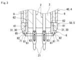
- FIG. 3 is a partially enlarged view of a cross-sectional view taken along line III--III in FIG.
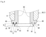
- FIG. 4 is a sectional view showing the first protrusion portion and its vicinity in the conductive rubber member included in the shield terminal module of the embodiment.
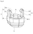
- FIG. 5 is a schematic perspective view of a state in which a resin member and a conductive member included in the shield terminal module of the embodiment are combined.
- FIG. 6 is a partially enlarged view of the VI-VI cross-sectional view of FIG.
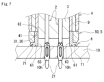
- FIG. 7 is a sectional view showing a state in which the shield terminal module of the embodiment is connected to a circuit board.
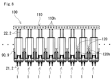
- FIG. 8 is a side view of a shield terminal module group in which a plurality of shield terminal modules of the embodiment are connected.
- each of the inner conductor terminal and the outer conductor terminal be connected to the circuit board without soldering. Further, it is desirable that the outer conductor terminal be connected to the circuit board in a ring shape so as to surround the entire circumference of the inner conductor terminal. A technique for connecting an outer conductor terminal to a circuit board in a circular manner without soldering has not been sufficiently studied.
- the inner conductor terminal will be referred to as a press-fit terminal
- the dielectric material will be referred to as a dielectric member
- the outer conductor terminal will be referred to as a shield member.
- One of the objects of the present disclosure is to provide a shield terminal module that can be connected to a circuit board without soldering.
- the shield terminal module of the present disclosure can be connected to a circuit board without soldering.
- the shield terminal module includes: A press-fit terminal having a rod-like shape, a dielectric member covering the press-fit terminal so that a first end and a second end of the press-fit terminal are exposed; a shield member covering the outer periphery of the dielectric member; a resin member attached to a region of the shield member near the first end; a conductive rubber member attached to the resin member, The resin member has a cylindrical shape surrounding the first end exposed from the dielectric member and the shield member, The conductive rubber member has a cylindrical shape disposed along the inner peripheral surface of the resin member, The conductive rubber member is a first end face facing a circuit board to which the first end is connected; a second end surface that is in contact with the end surface of the shield member; A first protrusion protruding from the first end surface in a direction along the axis of the conductive rubber member and continuously provided around the axis of the conductive rubber member.
- the terminals are press-fit terminals.
- a press-fit terminal is electrically and mechanically connected to a circuit board by being press-fitted into a through hole of the circuit board. Press-fit terminals are connected to conductive paths on a circuit board without soldering.
- the shield member is electrically connected to the circuit board via the conductive rubber member.
- the second end surface of the conductive rubber member is in contact with the end surface of the shield member.
- the first end surface of the conductive rubber member is arranged so as to face the circuit board.
- the conductive rubber member includes a first protrusion that protrudes beyond the first end surface. When the first end surface of the conductive rubber member contacts the circuit board, the first protrusion is pressed against the circuit board.
- the shield member is electrically connected to the shield circuit of the circuit board without soldering.
- the shield terminal module of (1) above can be connected to a circuit board without soldering.
- the conductive rubber member is provided with two grooves provided on the inner circumferential side and the outer circumferential side of the first protruding portion, and each of the two grooves is provided on the first protrusion.
- the protrusion may be recessed in the direction along the axis of the conductive rubber member relative to the first end surface so as to connect the side surface of the protrusion and the first end surface.
- the shield terminal module may come off from the circuit board due to the repulsive force from the circuit board acting on the first protrusion.
- the first protrusion deforms to fill the internal space of the groove due to the repulsive force. The deformation of the first protruding portion relieves the repulsive force, and prevents the shield terminal module from coming off from the circuit board due to the repulsive force.
- the first protrusion will easily deform to fill the internal space of the groove, and the shield terminal module will be damaged by the repulsive force against the circuit board. It is easy to prevent it from coming off the circuit board.
- the cross-sectional shape of the first protrusion may be triangular.
- the first protrusion When the cross-sectional shape of the first protrusion is triangular, the first protrusion is easily deformed by the repulsive force from the circuit board.
- the length of the first protruding portion protruding from the first end surface may be 0.15 mm or more and 0.4 mm or less.
- the protrusion length of the first protrusion is 0.15 mm or more, good contact between the first protrusion and the circuit board is easily ensured by deformation of the first protrusion.
- the protrusion length of the first protrusion is 0.4 mm or less, the repulsive force against the circuit board does not become too large, and the shield terminal module is easily prevented from coming off from the circuit board.
- the conductive rubber member protrudes beyond the second end surface in a direction along the axis of the conductive rubber member, and A second protruding portion continuously provided around the periphery may be provided.
- the conductive rubber member includes the second protrusion
- the second protrusion when the second end face of the conductive rubber member comes into contact with the end face of the shield member, the second protrusion is elastically deformed and comes into contact with the end face of the shield member. Due to the deformation of the second protruding portion, better contact between the conductive rubber member and the shield member is ensured than in the case where the second protruding portion is not provided.
- the hardness of the conductive rubber member may be 40 or more and 50 or less in Shore A hardness.
- the hardness of the conductive rubber member is 40 or more, the shape of the entire conductive rubber member is easily maintained, and the state in which the shield terminal module is connected to the circuit board is easily maintained. If the hardness of the conductive rubber member is 50 or less, it is likely to be deformed by repulsive force from the circuit board.
- the dielectric member includes an outer peripheral surface exposed from the shield member, and the outer peripheral surface faces the inner peripheral surface of the conductive rubber member. You can leave it there.
- the inner peripheral surface of the conductive rubber member is pressed against the exposed outer peripheral surface of the dielectric member.
- a distance corresponding to the thickness of the dielectric member is secured between the inner circumferential surface of the conductive rubber member and the first end of the press-fit terminal.
- the thickness of the dielectric member is the distance between the inner circumferential surface and the outer circumferential surface of the dielectric member.
- the inner peripheral surface of the dielectric member is in close contact with the outer peripheral surface of the press-fit terminal. Therefore, even if the conductive rubber member is elastically deformed, the distance between the conductive rubber member and the first end of the press-fit terminal is suppressed.
- the resin member has a fixing portion that fixes the resin member to the shield member with the second end face pressed against the end face of the shield member. You may prepare.
- the shield terminal module 1 includes a press-fit terminal 2, a dielectric member 3 (FIGS. 2 and 3), and a shield member 4.
- the shield member 4 includes a resin member 5 and a conductive rubber member 6.
- the resin member 5 is attached to the tip 40 (FIG. 3) of the shield member 4.
- the conductive rubber member 6 is attached to the resin member 5.
- the conductive rubber member 6 has a function of electrically connecting the circuit board 10 and the shield member 4 when the shield terminal module 1 is connected to the circuit board 10 shown in FIG. Each configuration will be explained in detail below.
- the press-fit terminal 2 is a rod-shaped member having a first end 21 and a second end 22, as shown in FIG.
- the first end portion 21 is press-fitted into a through hole 10h formed in the circuit board 10 shown in FIG.
- the press-fit terminal 2 and the circuit board 10 are electrically and mechanically connected.
- hatching of the press-fit terminal 2 is omitted.
- the shield terminal module 1 includes a plurality of press-fit terminals 2.
- the shield terminal module 1 of this example includes two press-fit terminals 2.
- the plurality of press-fit terminals 2 are arranged side by side at intervals.
- Each press-fit terminal 2 is a signal terminal.
- the dielectric member 3 is a resin molded body provided so as to cover the plurality of press-fit terminals 2, as shown in FIGS. 2 and 3.
- the dielectric member 3 is a columnar body.
- the dielectric member 3 is provided so that the first end 21 and second end 22 of each press-fit terminal 2 are exposed.
- the dielectric member 3 is arranged between adjacent press-fit terminals 2 and between each press-fit terminal 2 and a shield member 4, which will be described later.
- the dielectric member 3 is provided to ensure electrical insulation between the plurality of press-fit terminals 2 and between each press-fit terminal 2 and the shield member 4.
- the dielectric member 3 is designed to match the characteristic impedance at the frequency of the communication signal transmitted to the press-fit terminal 2.
- the dielectric member 3 is made of an insulating material.
- the cross-sectional shape of the dielectric member 3 in this example is a racetrack shape.
- the cross section of the dielectric member 3 is a cross section obtained by cutting the dielectric member 3 in a direction perpendicular to the axis of the dielectric member 3.
- the racetrack shape is a shape in which the ends of two linear parts that are parallel to each other and have the same length are connected by an arcuate part.
- the dielectric member 3 is covered with a shield member 4, which will be described later. That is, the outer peripheral surface of the dielectric member 3 faces the shield member 4.
- the dielectric member 3 of this example includes an exposed portion 30 exposed from the shield member 4.
- An outer circumferential surface 31 of the exposed portion 30 faces an inner circumferential surface 63 of a conductive rubber member 6, which will be described later.
- the outer circumferential surface 31 of the exposed portion 30 is in close contact with the inner circumferential surface 63 of the conductive rubber member 6.
- the shield member 4 is a cylindrical member provided so as to cover the outer periphery of the dielectric member 3, as shown in FIGS. 3 and 6.
- the shield member 4 of this example is a cylindrical member whose long axis is in the direction in which the plurality of press-fit terminals 2 are lined up.
- a rod-shaped member 9 which will be described later, is arranged in the direction in which the plurality of press-fit terminals 2 are lined up.
- the shield member 4 of this example also covers this rod-shaped member 9. A first end 21 and a second end 22 of the press-fit terminal 2 are exposed from the shield member 4.
- the shield member 4 has shielding performance to shield noise leaking from the press-fit terminal 2.
- the shield member 4 is made of, for example, a cast material.
- the shield member 4 made of cast material is difficult to form a gap on the circumferential surface of the shield member 4 .
- the shield member 4 made of cast material has excellent shielding performance.
- the material of the shield member 4 made of cast material is not particularly limited as long as it is a metal with high electrical conductivity.
- the material of the shield member 4 made of cast material is, for example, a zinc alloy.
- the shield member 4 may be made of a conductive resin material.
- the conductive resin material is, for example, a composite material in which a conductive filler is dispersed in a resin material.
- the resin material is, for example, polybutylene terephthalate (PBT).
- the material of the conductive filler is, for example, carbon black or metal.
- the tip portion 40 of the shield member 4 is a region of the shield member 4 that is close to the first end portion 21 of the press-fit terminal 2 .
- a second end surface 62 of a conductive rubber member 6, which will be described later, is in contact with the end surface 41 of the tip portion 40.
- the end surface 41 is a surface facing in the direction along the axis of the shield member 4.
- a part of the outer peripheral surface of the tip portion 40 is provided with an inclined surface 42 that projects outward from the outer edge of the end surface 41 toward the rear in the direction along the axis of the shield member 4. .
- the rear in the direction along the axis of the shield member 4 refers to the direction toward the second end 22 of the press-fit terminal 2 in the shield member 4 when viewed from the end surface 41.
- a step 43 is provided between the outer peripheral surface of the shield member 4 rearward of the tip 40 and the inclined surface 42 .
- the inclined surface 42 and the step 43 are provided at opposing locations on the outer peripheral surface of the shield member 4.
- the inclined surface 42 and the step 43 in this example are provided on a surface located in a direction perpendicular to both the direction in which the plurality of press-fit terminals 2 are lined up and the direction along the length of each press-fit terminal 2.
- a protrusion 512 of a resin member 5, which will be described later, is hooked onto the step 43.
- the resin member 5 is a cylindrical member attached to the tip portion 40 of the shield member 4, as shown in FIGS. 1, 3, and 6.
- the resin member 5 surrounds a portion of the first end portion 21 of the press-fit terminal 2 exposed from the dielectric member 3 and the shield member 4, as shown in FIGS. 3 and 6.
- the resin member 5 of this example includes a main body portion 50 and two fixing portions 51, as shown in FIGS. 5 and 6.
- the main body portion 50 is a cylindrical portion surrounding a part of the first end portion 21 of the press-fit terminal 2. The tip of the first end portion 21 is exposed from the resin member 5.
- the end face shape of the main body portion 50 substantially corresponds to the outer shape of the shield member 4. As shown in FIG. 2, the end face shape of the main body portion 50 is a racetrack shape that is long in the direction in which the plurality of press-fit terminals 2 are lined up.
- the two fixing parts 51 are provided facing each other, as shown in FIGS. 5 and 6. As shown in FIG. 6, the two fixing parts 51 of this example are surfaces located in a direction perpendicular to both the direction in which the plurality of press-fit terminals 2 are lined up and the direction along the length of each press-fit terminal 2. It is set in.
- Each fixing portion 51 is provided at a location close to the shield member 4 in the main body portion 50.
- Each fixing part 51 includes a leg part 511 and a protrusion 512, as shown in FIG.
- the leg portions 511 are plate pieces that protrude in the direction along the axis of the main body portion 50 .
- the protrusion 512 is provided at the tip of the leg portion 511.
- the protrusion 512 is provided on the surface where the two leg portions 511 face each other. As shown in FIG. 6, the protrusion 512 is caught on a step 43 provided at the tip 40 of the shield member 4.
- the fixing portion 51 is configured such that when the protrusion 512 is caught on the step 43, a second end surface 62 of a conductive rubber member 6, which will be described later, is pressed against the end surface 41 of the distal end portion 40.
- the conductive rubber member 6 is integrated with the resin member 5 as described later. Therefore, for example, the length of the leg portion 511 may be adjusted so that the second end surface 62 is pressed against the end surface 41 of the distal end portion 40 when the protrusion 512 is caught on the step 43.
- the conductive rubber member 6 is a cylindrical member attached to the inner peripheral surface of the resin member 5, as shown in FIGS. 1 to 4 and 6.
- the conductive rubber member 6 includes a first end surface 61, a second end surface 62, and a first protrusion 71, as shown in FIGS. 3 and 6.
- the first end surface 61 is a surface facing the circuit board 10 shown in FIG.
- the second end surface 62 is a surface that is in contact with the end surface 41 of the tip portion 40 of the shield member 4.
- the first protruding portion 71 is provided on the first end surface 61.
- the conductive rubber member 6 of this example further includes a first groove 81 and a second groove 82. The first groove 81 and the second groove 82 are also provided in the first end surface 61 .
- the conductive rubber member 6 of this example further includes a second protrusion portion 72, as shown in FIG.
- the second protruding portion 72 is provided on the second end surface 62.
- the second protrusion portion 72 is elastically deformed and crushed. Therefore, in FIGS. 3 and 6, the second protrusion portion 72 shown in FIG. 5 is not shown.
- the conductive rubber member 6 of this example includes a flange portion 65 at the end on the first end surface 61 side, as shown in FIGS. 3, 4, and 6.
- the flange portion 65 is an annular portion that protrudes outward in a direction perpendicular to the axis of the conductive rubber member 6 .
- the flange portion 65 covers the end surface of the main body portion 50 of the resin member 5.
- the first end surface 61 includes the end surface of the flange portion 65.
- the first protruding portion 71 protrudes from the first end surface 61 in the direction along the axis of the conductive rubber member 6.
- the first protruding portion 71 is pressed against the circuit board 10 when the shield terminal module 1 is connected to the circuit board 10 shown in FIG.
- the first protruding portion 71 pressed against the circuit board 10 is deformed by the repulsive force against the circuit board 10. The state in which the shield terminal module 1 is connected to the circuit board 10 will be described later.
- the first protruding portion 71 is continuously provided around the axis of the conductive rubber member 6.
- a first groove 81 and a second groove 82 which will be described later, are hatched.
- the first protruding portion 71 is arranged between the first groove 81 and the second groove 82.
- the shape of the first protruding portion 71 is annular, as shown in FIG.
- the first protruding portion 71 is annularly connected to the circuit board 10 shown in FIG. 7 . That is, the first protruding portion 71 is connected to the circuit board 10 so as to surround the entire circumference of the first end 21 of the press-fit terminal 2 connected to the circuit board 10.
- the cross-sectional shape of the first protrusion 71 is, for example, such that the width at the tip is smaller than the width at the base.
- This cross-sectional shape is, for example, a triangle, as shown in FIGS. 3, 4, and 6.
- the cross section of the first protruding portion 71 is a cross section obtained by cutting the first protruding portion 71 in a direction perpendicular to the direction in which the first protruding portion 71 extends.
- the cross-sectional shape of the first protruding portion 71 is triangular, the first protruding portion 71 is easily deformed by the repulsive force from the circuit board 10 shown in FIG. 7 .
- the cross-sectional shape of the first protrusion portion 71 may be semicircular or trapezoidal in which the width at the tip is smaller than the width at the base.
- the protrusion length 7L (FIG. 4) of the first protrusion portion 71 from the first end surface 61 is, for example, 0.15 mm or more and 0.4 mm or less.
- the protrusion length 7L is 0.15 mm or more, the deformation of the first protrusion 71 tends to ensure good contact between the first protrusion 71 and the circuit board 10 shown in FIG. 7 .
- the protrusion length 7L is 0.4 mm or less, the repulsive force against the circuit board 10 shown in FIG. 7 does not become too large, and the shield terminal module 1 is easily prevented from coming off from the circuit board 10.
- first groove 81 and the second groove 82 are continuously provided around the axis of the conductive rubber member 6 so as to sandwich the first protrusion 71 therebetween.
- Each of the first groove 81 and the second groove 82 is provided adjacent to the base of the first protruding portion 71, as shown in FIG.
- the first groove 81 is formed of a conductive rubber member on the inner peripheral side of the first protruding part 71 so as to connect the inner surface 711 of the first protruding part 71 and the first end face 61 flush with each other. It is recessed in the direction along the axis of 6.
- the second groove 82 is formed on the outer peripheral side of the first protrusion 71 so that the conductive rubber member 6 is connected flush with the outer surface 712 of the first protrusion 71 and the first end face 61 It is concave in the direction along the axis of. If the first groove 81 and the second groove 82 are provided adjacent to the base of the first protrusion 71, when the shield terminal module 1 is connected to the circuit board 10 shown in FIG. The strip portion 71 deforms so as to fill the internal space of each of the first groove 81 and the second groove 82. Due to this deformation of the first protruding portion 71, the repulsive force against the circuit board 10 is relaxed, and the shield terminal module 1 is difficult to come off from the circuit board 10. In other words, the state in which the shield terminal module 1 is connected to the circuit board 10 is easily maintained.
- the total area of the internal spaces of the first groove 81 and the second groove 82 is greater than or equal to the area of the first protrusion 71. Good.
- the internal spaces of the first groove 81 and the second groove 82 are shown with fine cross hatching, and the first protrusion 71 is shown with coarse cross hatching.
- the total area of the internal space of each of the first groove 81 and the second groove 82 is the total area of the area shown by fine cross hatching in FIG. 4 .
- the area of the first protrusion portion 71 is the area of the region shown by rough cross hatching in FIG. 4 .
- the first protruding portion 71 When the total area of the internal space is greater than or equal to the area of the first protruding portion 71, the first protruding portion 71 is likely to deform to fill the internal spaces of the first groove 81 and the second groove 82.
- the area of the internal space of the first groove 81 and the area of the internal space of the second groove 82 may be the same or different.
- the area of the internal space of each of the first groove 81 and the second groove 82 is a range that provides an escape margin for the first protrusion portion 71 that is deformed when the shield terminal module 1 is connected to the circuit board 10 shown in FIG. You can select as appropriate. Since the deformed first protruding portion 71 escapes into the first groove 81 and the second groove 82, the shield terminal module 1 is easily prevented from coming off from the circuit board 10 due to the repulsive force against the circuit board 10.
- each of the first groove 81 and the second groove 82 is, for example, a right-angled trapezoid, as shown in FIG.
- the cross section of the first groove 81 is a cross section obtained by cutting the first groove 81 in a direction perpendicular to the direction in which the first groove 81 extends.
- the outer circumferential surface of the first groove 81 is an inclined surface continuous with the inner surface 711 of the first protrusion 71 .
- the inner circumferential surface forming the first groove 81 is a flat surface extending along the axis of the conductive rubber member 6 .
- the cross section of the second groove 82 is a cross section obtained by cutting the second groove 82 in a direction perpendicular to the direction in which the second groove 82 extends.
- the inner circumferential surface constituting the second groove 82 is an inclined surface continuous with the outer surface 712 of the first protruding portion 71 .
- the outer peripheral side of the second groove 82 is a flat surface extending along the axis of the conductive rubber member 6 .
- the second protruding portion 72 protrudes beyond the second end surface 62 in the direction along the axis of the conductive rubber member 6.
- the second protruding portion 72 is elastically deformed and crushed when the conductive rubber member 6 is attached to the resin member 5 and the resin member 5 is attached to the shield member 4 shown in FIG.
- the shield member 4 and the conductive rubber member 6 are electrically well connected by the crushed second protrusion portion 72 .
- the second protruding portion 72 is continuously provided around the axis of the conductive rubber member 6.
- the shape of the second protruding portion 72 is annular. When the second protruding portion 72 is provided in an annular shape, the second protruding portion 72 is annularly connected to the shield member 4 shown in FIG. 1 .
- the cross-sectional shape of the second protrusion 72 is, for example, such that the width at the tip is smaller than the width at the base.
- This cross-sectional shape is, for example, a triangle.
- the cross section of the second protruding portion 72 is a cross section obtained by cutting the second protruding portion 72 in a direction perpendicular to the direction in which the second protruding portion 72 extends.
- the second protrusion 72 has a triangular cross-sectional shape, the second protrusion 72 is easily connected to the end surface 41 of the shield member 4 shown in FIG. 3 .
- the cross-sectional shape of the second protruding portion 72 may be semicircular or trapezoidal in which the width at the tip is smaller than the width at the base.
- the length of the second protrusion 72 protruding from the second end surface 62 is, for example, 0.15 mm or more and 0.4 mm or less.
- the protrusion length is 0.15 mm or more, the deformation of the second protrusion 72 tends to ensure good contact between the second protrusion 72 and the end surface 41 of the shield member 4 shown in FIG. 3 .
- the protrusion length is 0.4 mm or less, the repulsive force against the end surface 41 does not become too large, and the conductive rubber member 6 is difficult to come off from the shield member 4.
- Grooves may be provided on the inner circumferential side and the outer circumferential side of the second protruding portion 72, respectively. Each groove has the same structure as the first groove 81 and the second groove 82 described above.
- the conductive rubber member 6 is made of a composite material in which a conductive filler is dispersed in a rubber material.
- the rubber material is, for example, natural rubber or synthetic rubber.
- the rubber material is, for example, silicone rubber.
- the material of the conductive filler is, for example, carbon or metal.
- the hardness of the conductive rubber member 6 is, for example, 40 or more and 50 or less in Shore A hardness.
- the hardness of the conductive rubber member 6 depends on the hardness of the rubber material. When the hardness of the conductive rubber member 6 is 40 or more, the shape of the conductive rubber member 6 as a whole is easily maintained, and the state in which the shield terminal module 1 is connected to the circuit board 10 shown in FIG. 7 is easily maintained. If the hardness of the conductive rubber member 6 is 50 or less, the first protrusion 71 is likely to be deformed by the repulsive force from the circuit board 10 when the shield terminal module 1 is connected to the circuit board 10 shown in FIG. .
- the conductive rubber member 6 is, for example, an injection molded body integrally formed with the resin member 5.
- the resin member 5 and the conductive rubber member 6 can be handled as a single unit.
- the conductive rubber member 6 can be configured by two-color molding on the inner peripheral surface of the main body portion 50 of the resin member 5, for example, when molding the resin member 5 using a mold.
- the shield terminal module 1 of this example includes two rod-shaped members 9, as shown in FIGS. 1 and 3.
- the two rod-shaped members 9 are arranged on the outside in the direction in which the plurality of press-fit terminals 2 are lined up.
- the two rod-shaped members 9 are arranged parallel to the press-fit terminal 2.
- the two rod-shaped members 9 are part of a carrier used when manufacturing the shield terminal module 1. The career will be discussed later.
- a protruding piece 90 is provided at the first end of each rod-shaped member 9.
- the first end of each rod-shaped member 9 is located closer to the second end 22 of the press-fit terminal 2 than the first end 21 .
- a notch 90c is provided on the outer surface of the protruding piece 90.
- the shape of the notch 90c is, for example, semicircular. Most of each rod-shaped member 9 other than the protruding piece 90 is covered with the shield member 4. The material of the rod-shaped member 9 is, for example, the same metal as the press-fit terminal 2.
- the circuit board 10 is provided with a signal circuit and a ground circuit (not shown).
- the first end 21 of the press-fit terminal 2 is press-fitted into the through hole 10h of the circuit board 10 and electrically connected to the signal circuit of the circuit board 10.
- the conductive rubber member 6 When the first end portion 21 is press-fitted into the through hole 10h, the conductive rubber member 6 is pressed against the circuit board 10. When the conductive rubber member 6 is pressed against the circuit board 10, the conductive rubber member 6 is crushed so as to spread outward as a whole. At this time, the first protruding portion 71 (FIGS. 1 to 6) described above is deformed so that the tip thereof is tilted toward the outer circumferential side. The first protruding portion 71 is deformed by being crushed by the circuit board 10 so that the side surface thereof comes into contact with the circuit board 10 . The first protruding portion 71 of this example deforms so as to fill the internal space of each of the first groove 81 and the second groove 82.
- the first protruding portion 71 enters the first groove 81 and the second groove 82 and is crushed by the repulsive force against the circuit board 10 .
- the deformation of the first protruding portion 71 ensures good contact between the first protruding portion 71 and the circuit board 10 .
- the contact between the first protrusion portion 71 and the circuit board 10 is made over the entire circumference so as to surround the press-fit terminal 2 .
- the shield member 4 is connected to the ground circuit of the circuit board 10 via the conductive rubber member 6.
- the repulsive force against the circuit board 10 is alleviated, and the shield terminal module 1 is prevented from coming off from the circuit board 10. .
- the state in which the shield terminal module 1 is connected to the circuit board 10 is maintained well.
- the exposed portion 30 of the dielectric member 3 restricts the elastic deformation of the conductive rubber member 6 inward. Since the outer circumferential surface 31 of the exposed portion 30 and the inner circumferential surface 63 of the conductive rubber member 6 are in close contact, the distance corresponding to the thickness of the dielectric member 3 is between the inner circumferential surface 63 of the conductive rubber member 6 and the press-fit terminal. This is because it is secured between the first end portion 21 of No. 2 and the first end portion 21 of No. 2. Due to this interval, even if the conductive rubber member 6 is elastically deformed, contact between the conductive rubber member 6 and the first end portion 21 of the press-fit terminal 2 is suppressed.
- the press-fit terminal 2 is electrically connected to the signal circuit of the circuit board 10 by being press-fitted into the through hole 10h of the circuit board 10.
- the shield member 4 is electrically connected to the ground circuit of the circuit board 10 via the conductive rubber member 6. As described above, the shield terminal module 1 is connected to the circuit board 10 without soldering.
- the shield terminal module group 100 will be described with reference to FIG. 8.
- the shield terminal module group 100 includes a plurality of shield terminal modules 1 and a carrier that connects the plurality of shield terminal modules 1.
- the carrier of this example includes a first carrier 110 and a second carrier 120.
- the shield terminal module group 100 is wound onto a reel (not shown), for example. By winding the plurality of shield terminal modules 1 onto a reel as the shield terminal module group 100, the plurality of shield terminal modules 1 can be easily stored and the plurality of shield terminal modules 1 can be easily transported.
- the first carrier 110 connects the second ends 22 of adjacent press-fit terminals 2 so as to connect the plurality of shield terminal modules 1.
- the first carrier 110 is an elongated plate. In a state where the shield terminal module group 100 is wound onto a reel, the first carrier 110 is bent flatwise.
- Flatwise bending means bending the first carrier 110, which is an elongated plate, with the long side of the cross section thereof facing inward.
- the first carrier 110 includes a plurality of circular holes 110h provided at intervals in the length direction of the first carrier 110.
- the plurality of circular holes 110h are used, for example, when winding up and unwinding the shield terminal module group 100 onto a reel.
- the second carrier 120 is configured by connecting protrusions 90 of adjacent rod-shaped members 9 in adjacent shield terminal modules 1 to each other. When adjacent projecting pieces 90 are connected, one circular hole 120h is formed by the notch 90c (FIG. 1) provided in each projecting piece 90.
- the second carrier 120 is arranged between adjacent shield terminal modules 1. The circular holes 120h of each second carrier 120 are used, for example, when winding up and unwinding the shield terminal module group 100 onto a reel.
- the material of the first carrier 110 and the second carrier 120 is, for example, the same metal as the press-fit terminal 2.
- the reel (not shown) includes, for example, a winding drum and two collars.
- a shield terminal module group 100 is wound around the winding drum.
- a hole is provided in the center of the winding drum.
- the winding drum is rotatable around a rotating shaft inserted into the hole.
- the two collars are spaced apart from each other at both ends of the shaft of the winding drum.
- the shield terminal module group 100 is, for example, wound up in multiple layers on the winding body of a reel.
- an intervening member may be arranged between turns of the shield terminal module group 100 that overlap.
- the intervening member is, for example, a tape material that is continuous in the winding direction. When the intervening member is disposed, it is easy to prevent damage to the shield terminal module 1 caused by the inner turns and outer turns of the shield terminal module group 100 rubbing against each other.
- the shield terminal module group 100 is manufactured, for example, by sequentially performing the following first step, second step, third step, and fourth step.
- the first step is to prepare a long body in which a plurality of terminal groups are connected by a carrier.
- Each terminal group includes a plurality of press-fit terminals 2 and two rod-shaped members 9 arranged on the outside in the direction in which the plurality of press-fit terminals 2 are lined up.
- Each terminal group in this example includes two press-fit terminals 2.
- the length of the rod-shaped member 9 in each terminal group of this example is longer than that of the rod-shaped member 9 shown in FIG. Specifically, the first end of the rod-shaped member 9 in each terminal group is extended to a position aligned with the first end 21 of the press-fit terminal 2 .
- the plurality of terminal groups are connected by a first carrier 110, a second carrier 120, and a third carrier (not shown).
- the third carrier connects the first ends 21 of adjacent press-fit terminals 2 and the first ends of the rod-shaped members 9 so as to connect a plurality of terminal groups.
- the third carrier has the same configuration as the first carrier 110.
- the second step is a step of providing dielectric members 3 on each terminal group in the elongated body.
- the dielectric member 3 is provided so as to cover the plurality of press-fit terminals 2 in each terminal group. A first end 21 and a second end 22 of the press-fit terminal 2 are exposed from the dielectric member 3.
- the third step is a step of providing a shield member 4 around the outer periphery of the dielectric member 3 in the elongated body.
- the shield member 4 is also provided on the outer periphery of the rod-shaped member 9.
- the protruding piece 90 of the rod-shaped member 9 is exposed from the shield member 4.
- the fourth step is a step of attaching the resin member 5 and the conductive rubber member 6 to the tip portion 40 of the shield member 4 in the elongated body.
- the resin member 5 and the conductive rubber member 6 are integrally formed in advance.
- the shield terminal module group 100 shown in FIG. 8 shows a state in which the fourth step has been completed.
- the elongated body in each of the above steps is wound onto a reel (not shown), for example.
- Each carrier is used, for example, when winding up and unwinding a long body onto a reel.
Landscapes
- Shielding Devices Or Components To Electric Or Magnetic Fields (AREA)
- Details Of Connecting Devices For Male And Female Coupling (AREA)
Abstract
プレスフィット端子と、プレスフィット端子を覆っている誘電体部材と、誘電体部材の外周を覆っているシールド部材と、シールド部材に取り付けられた樹脂部材と、樹脂部材に取り付けられた導電ゴム部材と、を備え、導電ゴム部材は、プレスフィット端子の第一端部が接続される回路基板を臨む第一端面と、シールド部材の端面に接触している第二端面と、第一端面よりも導電ゴム部材の軸に沿った方向に突出しており、かつ導電ゴム部材の軸周りに連続して設けられた第一突条部と、を備える、シールド端子モジュール。
Description
本開示は、シールド端子モジュールに関する。
本出願は、2022年4月12日付の日本国出願の特願2022-065724に基づく優先権を主張し、前記日本国出願に記載された全ての記載内容を援用するものである。
本出願は、2022年4月12日付の日本国出願の特願2022-065724に基づく優先権を主張し、前記日本国出願に記載された全ての記載内容を援用するものである。
特許文献1は、内導体端子、内導体端子の外周に配置された誘電体、及び誘電体の外周に配置された外導体端子を備えるシールドコネクタを開示する。シールドコネクタは、回路基板の表面に取り付けられる。内導体端子は、回路基板の表面上の導電路に半田付けして接続される。外導体端子は、回路基板のシールド回路に半田付けして接続される。
本開示のシールド端子モジュールは、
棒状の形状を有するプレスフィット端子と、
前記プレスフィット端子の第一端部および第二端部が露出するように前記プレスフィット端子を覆っている誘電体部材と、
前記誘電体部材の外周を覆っているシールド部材と、
前記シールド部材における前記第一端部に近い領域に取り付けられた樹脂部材と、
前記樹脂部材に取り付けられた導電ゴム部材と、を備え、
前記樹脂部材の形状は、前記誘電体部材および前記シールド部材から露出した前記第一端部を囲んでいる筒状であり、
前記導電ゴム部材の形状は、前記樹脂部材の内周面に沿って配置された筒状であり、
前記導電ゴム部材は、
前記第一端部が接続される回路基板を臨む第一端面と、
前記シールド部材の端面に接触している第二端面と、
前記第一端面よりも前記導電ゴム部材の軸に沿った方向に突出しており、かつ前記導電ゴム部材の軸周りに連続して設けられた第一突条部と、を備える。
棒状の形状を有するプレスフィット端子と、
前記プレスフィット端子の第一端部および第二端部が露出するように前記プレスフィット端子を覆っている誘電体部材と、
前記誘電体部材の外周を覆っているシールド部材と、
前記シールド部材における前記第一端部に近い領域に取り付けられた樹脂部材と、
前記樹脂部材に取り付けられた導電ゴム部材と、を備え、
前記樹脂部材の形状は、前記誘電体部材および前記シールド部材から露出した前記第一端部を囲んでいる筒状であり、
前記導電ゴム部材の形状は、前記樹脂部材の内周面に沿って配置された筒状であり、
前記導電ゴム部材は、
前記第一端部が接続される回路基板を臨む第一端面と、
前記シールド部材の端面に接触している第二端面と、
前記第一端面よりも前記導電ゴム部材の軸に沿った方向に突出しており、かつ前記導電ゴム部材の軸周りに連続して設けられた第一突条部と、を備える。
[本開示が解決しようとする課題]
内導体端子及び外導体端子の各々は、回路基板に無半田で接続されることが望まれている。また、外導体端子は内導体端子の全周を囲むように環状に回路基板に接続されることが望まれる。外導体端子を環状に回路基板に無半田で接続する技術は、十分な検討がなされていない。
内導体端子及び外導体端子の各々は、回路基板に無半田で接続されることが望まれている。また、外導体端子は内導体端子の全周を囲むように環状に回路基板に接続されることが望まれる。外導体端子を環状に回路基板に無半田で接続する技術は、十分な検討がなされていない。
以下の説明では、内導体端子をプレスフィット端子、誘電体を誘電体部材、外導体端子をシールド部材と呼ぶ。
本開示は、無半田で回路基板に接続可能なシールド端子モジュールを提供することを目的の一つとする。
[本開示の効果]
本開示のシールド端子モジュールは、無半田で回路基板に接続可能である。
本開示のシールド端子モジュールは、無半田で回路基板に接続可能である。
[本開示の実施形態の説明]
最初に本開示の実施態様を列記して説明する。
最初に本開示の実施態様を列記して説明する。
(1)本開示の実施形態に係るシールド端子モジュールは、
棒状の形状を有するプレスフィット端子と、
前記プレスフィット端子の第一端部および第二端部が露出するように前記プレスフィット端子を覆っている誘電体部材と、
前記誘電体部材の外周を覆っているシールド部材と、
前記シールド部材における前記第一端部に近い領域に取り付けられた樹脂部材と、
前記樹脂部材に取り付けられた導電ゴム部材と、を備え、
前記樹脂部材の形状は、前記誘電体部材および前記シールド部材から露出した前記第一端部を囲んでいる筒状であり、
前記導電ゴム部材の形状は、前記樹脂部材の内周面に沿って配置された筒状であり、
前記導電ゴム部材は、
前記第一端部が接続される回路基板を臨む第一端面と、
前記シールド部材の端面に接触している第二端面と、
前記第一端面よりも前記導電ゴム部材の軸に沿った方向に突出しており、かつ前記導電ゴム部材の軸周りに連続して設けられた第一突条部と、を備える。
棒状の形状を有するプレスフィット端子と、
前記プレスフィット端子の第一端部および第二端部が露出するように前記プレスフィット端子を覆っている誘電体部材と、
前記誘電体部材の外周を覆っているシールド部材と、
前記シールド部材における前記第一端部に近い領域に取り付けられた樹脂部材と、
前記樹脂部材に取り付けられた導電ゴム部材と、を備え、
前記樹脂部材の形状は、前記誘電体部材および前記シールド部材から露出した前記第一端部を囲んでいる筒状であり、
前記導電ゴム部材の形状は、前記樹脂部材の内周面に沿って配置された筒状であり、
前記導電ゴム部材は、
前記第一端部が接続される回路基板を臨む第一端面と、
前記シールド部材の端面に接触している第二端面と、
前記第一端面よりも前記導電ゴム部材の軸に沿った方向に突出しており、かつ前記導電ゴム部材の軸周りに連続して設けられた第一突条部と、を備える。
上記(1)のシールド端子モジュールでは、端子がプレスフィット端子である。プレスフィット端子は、回路基板のスルーホールに圧入されることで回路基板に電気的及び機械的に接続される。プレスフィット端子は、無半田で回路基板の導電路に接続される。上記(1)のシールド端子モジュールでは、シールド部材は、導電ゴム部材を介して回路基板に電気的に接続される。導電ゴム部材の第二端面は、シールド部材の端面に接触している。導電ゴム部材の第一端面は、回路基板を臨むように配置されている。導電ゴム部材は、第一端面よりも突出した第一突条部を備える。導電ゴム部材の第一端面が回路基板に接触すると、第一突条部は回路基板に押し付けられる。導電ゴム部材は弾性変形することから、回路基板に接触した第一突条部は、回路基板に対する反発力で変形する。この第一突条部の変形によって、第一突条部と回路基板との接触が良好に確保される。導電ゴム部材がシールド部材及び回路基板の双方に接触されることで、シールド部材は、無半田で回路基板のシールド回路に電気的に接続される。以上より、上記(1)のシールド端子モジュールは、無半田で回路基板に接続可能である。
(2)上記(1)において、前記導電ゴム部材は、前記第一突条部の内周側と外周側にそれぞれ設けられた二つの溝を備え、前記二つの溝の各々は、前記第一突条部の側面と前記第一端面とをつなぐように前記第一端面よりも前記導電ゴム部材の軸に沿った方向に窪んでいてもよい。
第一突条部に作用する回路基板からの反発力によって、シールド端子モジュールが回路基板から抜けるおそれがある。第一突条部の根元に溝が設けられていると、シールド端子モジュールが回路基板に接続されると、上記反発力によって、第一突条部が溝の内部空間を埋めるように変形する。この第一突条部の変形によって、上記反発力が緩和され、上記反発力でシールド端子モジュールが回路基板から抜けることは抑制される。
(3)上記(2)において、前記導電ゴム部材の軸に沿って前記導電ゴム部材を切断した断面において、前記二つの溝の各々の内部空間の面積の合計は、前記第一突条部の面積以上であってもよい。
各溝の内部空間の体積の合計が第一突条部の体積以上であると、第一突条部が溝の内部空間を埋めるように変形し易く、回路基板に対する反発力でシールド端子モジュールが回路基板から抜けることが抑制され易い。
(4)上記(1)から(3)のいずれかにおいて、前記第一突条部の横断面形状は、三角形であってもよい。
第一突条部の横断面形状が三角形であると、第一突条部が回路基板からの反発力によって変形し易い。
(5)上記(1)から(4)のいずれかにおいて、前記第一突条部における前記第一端面からの突出長さは、0.15mm以上0.4mm以下であってもよい。
第一突条部の突出長さが0.15mm以上であると、第一突条部の変形によって、第一突条部と回路基板との接触が良好に確保され易い。第一突条部の突出長さが0.4mm以下であると、回路基板に対する反発力が大きくなり過ぎず、シールド端子モジュールが回路基板から抜けることが抑制され易い。
(6)上記(1)から(5)のいずれかにおいて、前記導電ゴム部材は、前記第二端面よりも前記導電ゴム部材の軸に沿った方向に突出しており、かつ前記導電ゴム部材の軸周りに連続して設けられた第二突条部を備えてもよい。
導電ゴム部材が第二突条部を備えると、導電ゴム部材の第二端面がシールド部材の端面に接触すると、第二突条部は弾性変形することでシールド部材の端面に接触する。この第二突条部の変形によって、第二突条部を備えない場合に比較して、導電ゴム部材とシールド部材との接触が良好に確保される。
(7)上記(1)から(6)のいずれかにおいて、前記導電ゴム部材の硬度は、ショアA硬度で40以上50以下であってもよい。
導電ゴム部材の硬度が40以上であると、導電ゴム部材全体の形状が保持され易く、シールド端子モジュールが回路基板に接続された状態が保持され易い。導電ゴム部材の硬度が50以下であると、回路基板からの反発力で変形し易い。
(8)上記(1)から(7)のいずれかにおいて、前記誘電体部材は、前記シールド部材から露出された外周面を備え、前記外周面は、前記導電ゴム部材の内周面に面していてもよい。
誘電体部材がシールド部材から露出されていると、導電ゴム部材の内周面が誘電体部材の露出された外周面に押し付けられる。この押し付けによって、誘電体部材の厚さに対応した間隔が導電ゴム部材の内周面とプレスフィット端子の第一端部との間に確保される。誘電体部材の厚さは、誘電体部材の内周面と外周面との間の距離である。誘電体部材の内周面は、プレスフィット端子の外周面に密着している。そのため、上記間隔によって、導電ゴム部材が弾性変形しても、導電ゴム部材とプレスフィット端子の第一端部との接触が抑制される。
(9)上記(1)から(8)のいずれかにおいて、前記樹脂部材は、前記シールド部材の端面に前記第二端面が押し付けられた状態で前記樹脂部材を前記シールド部材に固定する固定部を備えてもよい。
樹脂部材とシールド部材とが固定部で固定されていると、導電ゴム部材とシールド部材との接触が良好に確保される。
[本開示の実施形態の詳細]
本開示の実施形態の具体例を、以下に図面を参照しつつ説明する。図中の同一符号は同一名称物を示す。各図面では、説明の便宜上、構成の一部を誇張又は簡略化して示す場合がある。図面における各部の寸法比も実際と異なる場合がある。なお、本発明はこれらの例示に限定されるものではなく、請求の範囲によって示され、請求の範囲と均等の意味及び範囲内でのすべての変更が含まれることが意図される。
本開示の実施形態の具体例を、以下に図面を参照しつつ説明する。図中の同一符号は同一名称物を示す。各図面では、説明の便宜上、構成の一部を誇張又は簡略化して示す場合がある。図面における各部の寸法比も実際と異なる場合がある。なお、本発明はこれらの例示に限定されるものではなく、請求の範囲によって示され、請求の範囲と均等の意味及び範囲内でのすべての変更が含まれることが意図される。
<シールド端子モジュール>
図1から図7を参照して、実施形態に係るシールド端子モジュール1を説明する。シールド端子モジュール1は、図1に示すように、プレスフィット端子2、誘電体部材3(図2,図3)、及びシールド部材4を備える。シールド端子モジュール1の特徴の一つは、シールド部材4に樹脂部材5及び導電ゴム部材6を備える点にある。樹脂部材5は、シールド部材4の先端部40(図3)に取り付けられている。導電ゴム部材6は、樹脂部材5に取り付けられている。導電ゴム部材6は、シールド端子モジュール1が図7に示す回路基板10に接続された際に、回路基板10とシールド部材4とを電気的に接続する機能を有する。以下、各構成を詳細に説明する。
図1から図7を参照して、実施形態に係るシールド端子モジュール1を説明する。シールド端子モジュール1は、図1に示すように、プレスフィット端子2、誘電体部材3(図2,図3)、及びシールド部材4を備える。シールド端子モジュール1の特徴の一つは、シールド部材4に樹脂部材5及び導電ゴム部材6を備える点にある。樹脂部材5は、シールド部材4の先端部40(図3)に取り付けられている。導電ゴム部材6は、樹脂部材5に取り付けられている。導電ゴム部材6は、シールド端子モジュール1が図7に示す回路基板10に接続された際に、回路基板10とシールド部材4とを電気的に接続する機能を有する。以下、各構成を詳細に説明する。
≪プレスフィット端子≫
プレスフィット端子2は、図1に示すように、第一端部21及び第二端部22を有する棒状の部材である。第一端部21は、図7に示す回路基板10に形成されたスルーホール10hに圧入される。第一端部21がスルーホール10hに圧入されることで、プレスフィット端子2と回路基板10とが電気的及び機械的に接続される。図3、図6、及び図7では、プレスフィット端子2のハッチングを省略している。
プレスフィット端子2は、図1に示すように、第一端部21及び第二端部22を有する棒状の部材である。第一端部21は、図7に示す回路基板10に形成されたスルーホール10hに圧入される。第一端部21がスルーホール10hに圧入されることで、プレスフィット端子2と回路基板10とが電気的及び機械的に接続される。図3、図6、及び図7では、プレスフィット端子2のハッチングを省略している。
シールド端子モジュール1は、複数のプレスフィット端子2を備える。本例のシールド端子モジュール1は、二つのプレスフィット端子2を備える。複数のプレスフィット端子2は、互いに間隔をあけて横並びに配置されている。各プレスフィット端子2は、信号端子である。
≪誘電体部材≫
誘電体部材3は、図2及び図3に示すように、複数のプレスフィット端子2を覆うように設けられた樹脂成形体である。誘電体部材3は柱状体である。誘電体部材3は、各プレスフィット端子2の第一端部21及び第二端部22が露出するように設けられている。誘電体部材3は、隣り合うプレスフィット端子2の間、及び各プレスフィット端子2と後述するシールド部材4との間に配置されている。誘電体部材3は、複数のプレスフィット端子2同士の電気的絶縁、及び各プレスフィット端子2とシールド部材4との電気的絶縁を確保するために設けられている。誘電体部材3は、プレスフィット端子2に伝送される通信信号の周波数での特性インピーダンスとの整合が取れるように設計されている。誘電体部材3は、絶縁材料で構成されている。
誘電体部材3は、図2及び図3に示すように、複数のプレスフィット端子2を覆うように設けられた樹脂成形体である。誘電体部材3は柱状体である。誘電体部材3は、各プレスフィット端子2の第一端部21及び第二端部22が露出するように設けられている。誘電体部材3は、隣り合うプレスフィット端子2の間、及び各プレスフィット端子2と後述するシールド部材4との間に配置されている。誘電体部材3は、複数のプレスフィット端子2同士の電気的絶縁、及び各プレスフィット端子2とシールド部材4との電気的絶縁を確保するために設けられている。誘電体部材3は、プレスフィット端子2に伝送される通信信号の周波数での特性インピーダンスとの整合が取れるように設計されている。誘電体部材3は、絶縁材料で構成されている。
本例の誘電体部材3の横断面形状は、レーストラック形状である。誘電体部材3の横断面は、誘電体部材3を誘電体部材3の軸と直交する方向に切断した断面である。レーストラック形状とは、互いに平行かつ同じ長さの二つの直線部の端部同士を円弧部でつないだ形状である。
誘電体部材3は、図3に示すように、後述するシールド部材4で覆われている。つまり、誘電体部材3の外周面は、シールド部材4に面している。本例の誘電体部材3は、シールド部材4から露出された露出部30を備える。露出部30の外周面31は、後述する導電ゴム部材6の内周面63に面している。本例では、露出部30の外周面31は、導電ゴム部材6の内周面63に密着している。誘電体部材3に露出部30が設けられていることで、誘電体部材3の厚さに対応した間隔が導電ゴム部材6の内周面63とプレスフィット端子2の第一端部21との間に確保される。誘電体部材3の厚さは、誘電体部材3の外周面と、誘電体部材3におけるプレスフィット端子2との接触面との間の距離である。
≪シールド部材≫
シールド部材4は、図3及び図6に示すように、誘電体部材3の外周を覆うように設けられた筒状の部材である。本例のシールド部材4は、複数のプレスフィット端子2が並んだ方向を長軸とする筒状の部材である。複数のプレスフィット端子2が並んだ方向には、図3に示すように、後述する棒状部材9が配置されている。本例のシールド部材4は、この棒状部材9も覆っている。プレスフィット端子2の第一端部21及び第二端部22は、シールド部材4から露出している。シールド部材4は、プレスフィット端子2から漏れるノイズを遮蔽するシールド性能を有する。
シールド部材4は、図3及び図6に示すように、誘電体部材3の外周を覆うように設けられた筒状の部材である。本例のシールド部材4は、複数のプレスフィット端子2が並んだ方向を長軸とする筒状の部材である。複数のプレスフィット端子2が並んだ方向には、図3に示すように、後述する棒状部材9が配置されている。本例のシールド部材4は、この棒状部材9も覆っている。プレスフィット端子2の第一端部21及び第二端部22は、シールド部材4から露出している。シールド部材4は、プレスフィット端子2から漏れるノイズを遮蔽するシールド性能を有する。
シールド部材4は、例えば鋳造材で構成されている。鋳造材で構成されたシールド部材4は、シールド部材4の周面に隙間が構成され難い。鋳造材で構成されたシールド部材4は、シールド性能に優れる。鋳造材で構成されたシールド部材4の材質は、電気伝導率が高い金属であれば特に限定されない。鋳造材で構成されたシールド部材4の材質は、例えば亜鉛合金である。
シールド部材4は、導電性樹脂材で構成されていてもよい。導電性樹脂材は、例えば樹脂材料に導電性フィラーが分散された複合材である。樹脂材料の材質は、例えばポリブチレンテレフタレート(PBT)である。導電性フィラーの材質は、例えばカーボンブラック又は金属である。
シールド部材4の先端部40には、後述する樹脂部材5が取り付けられている。シールド部材4の先端部40は、シールド部材4におけるプレスフィット端子2の第一端部21に近い領域である。先端部40の端面41には、後述する導電ゴム部材6の第二端面62が接触している。端面41は、シールド部材4の軸に沿った方向に向く面である。図6に示すように、先端部40の外周面の一部には、端面41の外縁からシールド部材4の軸に沿った方向の後方に向かうに従って外に張り出す傾斜面42が設けられている。シールド部材4の軸に沿った方向の後方とは、端面41から見てシールド部材4におけるプレスフィット端子2の第二端部22に向かう方向のことである。シールド部材4における先端部40よりも後方の外周面と傾斜面42との間には、段差43が設けられている。傾斜面42及び段差43は、シールド部材4の外周面における向かい合う箇所に設けられている。本例の傾斜面42及び段差43は、複数のプレスフィット端子2が並んだ方向及び各プレスフィット端子2の長さに沿った方向の双方と直交する方向に位置する面に設けられている。段差43には、後述する樹脂部材5の突起512が引っ掛けられている。
≪樹脂部材≫
樹脂部材5は、図1、図3、及び図6に示すように、シールド部材4の先端部40に取り付けられた筒状の部材である。樹脂部材5は、図3及び図6に示すように、誘電体部材3及びシールド部材4から露出したプレスフィット端子2の第一端部21の一部を囲んでいる。本例の樹脂部材5は、図5及び図6に示すように、本体部50と二つの固定部51を備える。
樹脂部材5は、図1、図3、及び図6に示すように、シールド部材4の先端部40に取り付けられた筒状の部材である。樹脂部材5は、図3及び図6に示すように、誘電体部材3及びシールド部材4から露出したプレスフィット端子2の第一端部21の一部を囲んでいる。本例の樹脂部材5は、図5及び図6に示すように、本体部50と二つの固定部51を備える。
本体部50は、プレスフィット端子2の第一端部21の一部を囲んでいる筒状の部分である。第一端部21の先端は、樹脂部材5から露出されている。本体部50の端面形状は、シールド部材4の外形に略対応している。本体部50の端面形状は、図2に示すように、複数のプレスフィット端子2が並んだ方向に長いレーストラック状の形状である。
二つの固定部51は、図5及び図6に示すように、互いに向かい合って設けられている。本例の二つの固定部51は、図6に示すように、複数のプレスフィット端子2が並んだ方向及び各プレスフィット端子2の長さに沿った方向の双方と直交する方向に位置する面に設けられている。各固定部51は、本体部50におけるシールド部材4に近い箇所に設けられている。各固定部51は、図5に示すように、脚部511と突起512を備える。脚部511は、本体部50の軸に沿った方向に突出した板片である。突起512は、脚部511の先端に設けられている。突起512は、二つの脚部511が互いに向かい合う面に設けられている。突起512は、図6に示すように、シールド部材4の先端部40に設けられた段差43に引っ掛かっている。固定部51は、突起512が段差43に引っ掛かった状態において、先端部40の端面41に後述する導電ゴム部材6の第二端面62が押し付けられるように構成されている。導電ゴム部材6は、後述するように樹脂部材5と一体になっている。そのため、例えば、突起512が段差43に引っ掛かった状態において、先端部40の端面41に第二端面62が押し付けられるように、脚部511の長さが調整されるとよい。
≪導電ゴム部材≫
導電ゴム部材6は、図1から図4及び図6に示すように、樹脂部材5の内周面に取り付けられた筒状の部材である。導電ゴム部材6は、図3及び図6に示すように、第一端面61、第二端面62、及び第一突条部71を備える。第一端面61は、図7に示す回路基板10に臨む面である。第二端面62は、シールド部材4の先端部40の端面41に接触している面である。第一突条部71は、第一端面61に設けられている。本例の導電ゴム部材6は、第一溝81及び第二溝82を更に備える。第一溝81及び第二溝82も、第一端面61に設けられている。
導電ゴム部材6は、図1から図4及び図6に示すように、樹脂部材5の内周面に取り付けられた筒状の部材である。導電ゴム部材6は、図3及び図6に示すように、第一端面61、第二端面62、及び第一突条部71を備える。第一端面61は、図7に示す回路基板10に臨む面である。第二端面62は、シールド部材4の先端部40の端面41に接触している面である。第一突条部71は、第一端面61に設けられている。本例の導電ゴム部材6は、第一溝81及び第二溝82を更に備える。第一溝81及び第二溝82も、第一端面61に設けられている。
本例の導電ゴム部材6は、図5に示すように、第二突条部72を更に備える。第二突条部72は、第二端面62に設けられている。導電ゴム部材6が樹脂部材5に取り付けられ、かつ樹脂部材5がシールド部材4に取り付けられた状態では、第二突条部72は弾性変形して押し潰されている。そのため、図3及び図6では、図5に示す第二突条部72が表れていない。
本例の導電ゴム部材6は、図3、図4、及び図6に示すように、第一端面61側の端部にフランジ部65を備える。フランジ部65は、導電ゴム部材6の軸と直交する方向の外方に突出している環状の部分である。フランジ部65は、樹脂部材5の本体部50の端面を覆っている。第一端面61は、フランジ部65の端面を含む。
〔第一突条部〕
第一突条部71は、図3、図4、及び図6に示すように、第一端面61よりも導電ゴム部材6の軸に沿った方向に突出している。第一突条部71は、シールド端子モジュール1が図7に示す回路基板10に接続された状態では、回路基板10に押し付けられる。回路基板10に押し付けられた第一突条部71は、回路基板10に対する反発力で変形する。シールド端子モジュール1が回路基板10に接続された状態については後述する。
第一突条部71は、図3、図4、及び図6に示すように、第一端面61よりも導電ゴム部材6の軸に沿った方向に突出している。第一突条部71は、シールド端子モジュール1が図7に示す回路基板10に接続された状態では、回路基板10に押し付けられる。回路基板10に押し付けられた第一突条部71は、回路基板10に対する反発力で変形する。シールド端子モジュール1が回路基板10に接続された状態については後述する。
第一突条部71は、図2に示すように、導電ゴム部材6の軸周りに連続して設けられている。図2では、分かり易いように、後述する第一溝81及び第二溝82にハッチングを付している。第一突条部71は、第一溝81と第二溝82との間に配置されている。導電ゴム部材6の軸に沿った方向から見て、第一突条部71の形状は、図2に示すように、環状である。第一突条部71が環状に設けられていると、第一突条部71が図7に示す回路基板10に環状に接続される。つまり、第一突条部71は、回路基板10に接続されたプレスフィット端子2の第一端部21の全周を囲むように回路基板10に接続される。
第一突条部71の横断面形状は、例えば、先端の幅が根元の幅よりも小さい形状である。この横断面形状は、図3、図4及び図6に示すように、例えば三角形である。第一突条部71の横断面は、第一突条部71を第一突条部71が延びる方向と直交する方向に切断した断面である。第一突条部71の横断面形状が三角形であると、第一突条部71が図7に示す回路基板10からの反発力によって変形し易い。第一突条部71の横断面形状は、半円状、又は先端の幅が根元の幅よりも小さい台形状であってもよい。
第一突条部71における第一端面61からの突出長さ7L(図4)は、例えば0.15mm以上0.4mm以下である。上記突出長さ7Lが0.15mm以上であると、第一突条部71の変形によって、第一突条部71と図7に示す回路基板10との接触が良好に確保され易い。上記突出長さ7Lが0.4mm以下であると、図7に示す回路基板10に対する反発力が大きくなり過ぎず、シールド端子モジュール1が回路基板10から抜けることが抑制され易い。
〔第一溝及び第二溝〕
第一溝81及び第二溝82は、図2に示すように、第一突条部71を挟むように導電ゴム部材6の軸周りに連続して設けられている。第一溝81及び第二溝82の各々は、図4に示すように、第一突条部71の根元に隣接するように設けられている。第一溝81は、第一突条部71の内周側において、第一突条部71の内側面711と第一端面61とを面一につなぐように第一端面61よりも導電ゴム部材6の軸に沿った方向に窪んでいる。第二溝82は、第一突条部71の外周側において、第一突条部71の外側面712と第一端面61とを面一につなぐように第一端面61よりも導電ゴム部材6の軸に沿った方向に窪んでいる。第一突条部71の根元に隣接するように第一溝81及び第二溝82が設けられていると、シールド端子モジュール1が図7に示す回路基板10に接続された際、第一突条部71が第一溝81及び第二溝82の各々の内部空間を埋めるように変形する。この第一突条部71の変形によって、回路基板10に対する反発力が緩和され、シールド端子モジュール1が回路基板10から抜け難い。つまり、シールド端子モジュール1が回路基板10に接続された状態が維持され易い。
第一溝81及び第二溝82は、図2に示すように、第一突条部71を挟むように導電ゴム部材6の軸周りに連続して設けられている。第一溝81及び第二溝82の各々は、図4に示すように、第一突条部71の根元に隣接するように設けられている。第一溝81は、第一突条部71の内周側において、第一突条部71の内側面711と第一端面61とを面一につなぐように第一端面61よりも導電ゴム部材6の軸に沿った方向に窪んでいる。第二溝82は、第一突条部71の外周側において、第一突条部71の外側面712と第一端面61とを面一につなぐように第一端面61よりも導電ゴム部材6の軸に沿った方向に窪んでいる。第一突条部71の根元に隣接するように第一溝81及び第二溝82が設けられていると、シールド端子モジュール1が図7に示す回路基板10に接続された際、第一突条部71が第一溝81及び第二溝82の各々の内部空間を埋めるように変形する。この第一突条部71の変形によって、回路基板10に対する反発力が緩和され、シールド端子モジュール1が回路基板10から抜け難い。つまり、シールド端子モジュール1が回路基板10に接続された状態が維持され易い。
導電ゴム部材6の軸に沿って導電ゴム部材6を切断した断面において、第一溝81及び第二溝82の各々の内部空間の面積の合計は、第一突条部71の面積以上であるとよい。図4の左側では、第一溝81及び第二溝82の各内部空間を細かいクロスハッチングで示し、第一突条部71を粗いクロスハッチングで示している。第一溝81及び第二溝82の各々の内部空間の面積の合計は、図4の細かいクロスハッチングで示す領域の面積の合計である。第一突条部71の面積は、図4の粗いクロスハッチングで示す領域の面積である。上記内部空間の面積の合計が第一突条部71の面積以上であると、第一突条部71が第一溝81及び第二溝82の内部空間を埋めるように変形し易い。第一溝81の内部空間の面積と第二溝82の内部空間の面積とは、同じであってもよいし、異なっていてもよい。第一溝81及び第二溝82の各々の内部空間の面積は、シールド端子モジュール1が図7に示す回路基板10に接続された際に変形した第一突条部71の逃げ代となる範囲で適宜選択できる。変形した第一突条部71が第一溝81及び第二溝82に逃げることで、回路基板10に対する反発力でシールド端子モジュール1が回路基板10から抜けることが抑制され易い。
第一溝81及び第二溝82の各横断面形状は、図4に示すように、例えば直角台形である。第一溝81の横断面は、第一溝81を第一溝81が延びる方向と直交する方向に切断した断面である。第一溝81を構成する外周側の面は、第一突条部71の内側面711に連続した傾斜面である。第一溝81を構成する内周側の面は、導電ゴム部材6の軸に沿った平坦面である。第二溝82の横断面は、第二溝82を第二溝82が延びる方向と直交する方向に切断した断面である。第二溝82を構成する内周側の面は、第一突条部71の外側面712に連続した傾斜面である。第二溝82を構成する外周側の面は、導電ゴム部材6の軸に沿った平坦面である。第一溝81及び第二溝82の各横断面形状が上記直角台形であると、第一突条部71が回路基板10に対する反発力によって第一溝81及び第二溝82に逃げるように変形し易い。第一溝81及び第二溝82の各横断面形状は、三角形、四角形、又は半円形といった他の形状でもよい。
〔第二突条部〕
第二突条部72は、図5に示すように、第二端面62よりも導電ゴム部材6の軸に沿った方向に突出している。第二突条部72は、導電ゴム部材6が樹脂部材5に取り付けられ、かつ樹脂部材5が図3に示すシールド部材4に取り付けられた状態では、弾性変形して押し潰されている。押し潰された第二突条部72によって、シールド部材4と導電ゴム部材6とは電気的に良好に接続されている。
第二突条部72は、図5に示すように、第二端面62よりも導電ゴム部材6の軸に沿った方向に突出している。第二突条部72は、導電ゴム部材6が樹脂部材5に取り付けられ、かつ樹脂部材5が図3に示すシールド部材4に取り付けられた状態では、弾性変形して押し潰されている。押し潰された第二突条部72によって、シールド部材4と導電ゴム部材6とは電気的に良好に接続されている。
第二突条部72は、導電ゴム部材6の軸周りに連続して設けられている。第二突条部72の形状は環状である。第二突条部72が環状に設けられていると、第二突条部72が図1に示すシールド部材4に環状に接続される。
第二突条部72の横断面形状は、例えば、先端の幅が根元の幅よりも小さい形状である。この横断面形状は、例えば三角形である。第二突条部72の横断面は、第二突条部72を第二突条部72が延びる方向と直交する方向に切断した断面である。第二突条部72の横断面形状が三角形であると、第二突条部72が図3に示すシールド部材4の端面41に良好に接続され易い。第二突条部72の横断面形状は、半円状、又は先端の幅が根元の幅よりも小さい台形状であってもよい。
第二突条部72における第二端面62からの突出長さは、例えば0.15mm以上0.4mm以下である。上記突出長さが0.15mm以上であると、第二突条部72の変形によって、第二突条部72と図3に示すシールド部材4の端面41との接触が良好に確保され易い。上記突出長さが0.4mm以下であると、端面41に対する反発力が大きくなり過ぎず、導電ゴム部材6がシールド部材4から外れ難い。
第二突条部72の内周側と外周側にそれぞれ図示しない溝が設けられていてもよい。各溝は、上述した第一溝81及び第二溝82の構成と同じである。
〔材質〕
導電ゴム部材6は、ゴム材料に導電性フィラーが分散された複合材で構成されている。ゴム材料は、例えば、天然ゴム又は合成ゴムである。ゴム材料は、例えばシリコンゴムである。導電性フィラーの材質は、例えば、カーボン又は金属である。
導電ゴム部材6は、ゴム材料に導電性フィラーが分散された複合材で構成されている。ゴム材料は、例えば、天然ゴム又は合成ゴムである。ゴム材料は、例えばシリコンゴムである。導電性フィラーの材質は、例えば、カーボン又は金属である。
導電ゴム部材6の硬度は、例えばショアA硬度で40以上50以下である。導電ゴム部材6の硬度は、上記ゴム材料の硬度による。導電ゴム部材6の硬度が40以上であると、導電ゴム部材6全体の形状が保持され易く、シールド端子モジュール1が図7に示す回路基板10に接続された状態が保持され易い。導電ゴム部材6の硬度が50以下であると、シールド端子モジュール1が図7に示す回路基板10に接続された状態で、回路基板10からの反発力で第一突条部71が変形し易い。
導電ゴム部材6は、例えば、樹脂部材5と一体に構成された射出成形体である。この場合、樹脂部材5と導電ゴム部材6とを一体物として取り扱うことができる。導電ゴム部材6は、例えば、金型を用いて樹脂部材5を成形する際に、樹脂部材5の本体部50の内周面に二色成形して構成することができる。
≪棒状部材≫
本例のシールド端子モジュール1は、図1及び図3に示すように、二つの棒状部材9を備える。二つの棒状部材9は、複数のプレスフィット端子2が並んだ方向の外側に配置されている。二つの棒状部材9は、プレスフィット端子2と平行に配置されている。二つの棒状部材9は、シールド端子モジュール1を製造する際に用いられるキャリアの一部である。キャリアについては後述する。各棒状部材9の第一端部には、突片90が設けられている。各棒状部材9の第一端部は、プレスフィット端子2の第一端部21よりも第二端部22の近くに位置する端部である。突片90の外側面には、切欠き90cが設けられている。切欠き90cの形状は、例えば半円形である。各棒状部材9における突片90以外の大部分は、シールド部材4で覆われている。棒状部材9の材質は、例えばプレスフィット端子2と同じ金属である。
本例のシールド端子モジュール1は、図1及び図3に示すように、二つの棒状部材9を備える。二つの棒状部材9は、複数のプレスフィット端子2が並んだ方向の外側に配置されている。二つの棒状部材9は、プレスフィット端子2と平行に配置されている。二つの棒状部材9は、シールド端子モジュール1を製造する際に用いられるキャリアの一部である。キャリアについては後述する。各棒状部材9の第一端部には、突片90が設けられている。各棒状部材9の第一端部は、プレスフィット端子2の第一端部21よりも第二端部22の近くに位置する端部である。突片90の外側面には、切欠き90cが設けられている。切欠き90cの形状は、例えば半円形である。各棒状部材9における突片90以外の大部分は、シールド部材4で覆われている。棒状部材9の材質は、例えばプレスフィット端子2と同じ金属である。
<シールド端子モジュールが回路基板に接続された状態>
図7を参照して、シールド端子モジュール1が回路基板10に接続された状態を説明する。回路基板10には、図示しない信号回路と接地回路が設けられている。
図7を参照して、シールド端子モジュール1が回路基板10に接続された状態を説明する。回路基板10には、図示しない信号回路と接地回路が設けられている。
プレスフィット端子2の第一端部21は、回路基板10のスルーホール10hに圧入され、回路基板10の信号回路に電気的に接続される。
第一端部21がスルーホール10hに圧入されると、導電ゴム部材6が回路基板10に押し付けられる。導電ゴム部材6は、回路基板10に押し付けられると、全体的に外周側に広がるように押し潰される。このとき、上述した第一突条部71(図1から図6)は、先端が外周側に倒れるように変形する。第一突条部71は、側面が回路基板10に接触するように回路基板10に押し潰されて変形する。本例の第一突条部71は、第一溝81及び第二溝82の各々の内部空間を埋めるように変形する。言い換えると、第一突条部71は、回路基板10に対する反発力によって、第一溝81及び第二溝82に入り込んで押し潰される。第一突条部71の変形によって、第一突条部71と回路基板10との接触が良好に確保される。第一突条部71と回路基板10との接触は、プレスフィット端子2を囲むように全周にわたって行われる。シールド部材4は、この導電ゴム部材6を介して回路基板10の接地回路に接続される。第一突条部71が第一溝81及び第二溝82に入り込むように変形することで、回路基板10に対する反発力が緩和され、シールド端子モジュール1が回路基板10から抜けることは抑制される。つまり、シールド端子モジュール1が回路基板10に接続された状態が良好に維持される。
本例では、誘電体部材3の露出部30によって、導電ゴム部材6の内側への弾性変形は規制される。露出部30の外周面31と導電ゴム部材6の内周面63とが密着しているため、誘電体部材3の厚さに対応した間隔が導電ゴム部材6の内周面63とプレスフィット端子2の第一端部21との間に確保されているからである。この間隔によって、導電ゴム部材6が弾性変形しても、導電ゴム部材6とプレスフィット端子2の第一端部21との接触は抑制される。
プレスフィット端子2は、回路基板10のスルーホール10hに圧入されることで回路基板10の信号回路に電気的に接続される。シールド部材4は、導電ゴム部材6を介して回路基板10の接地回路に電気的に接続される。以上により、シールド端子モジュール1は、無半田で回路基板10に接続される。
<シールド端子モジュール群>
図8を参照して、シールド端子モジュール群100を説明する。シールド端子モジュール群100は、複数のシールド端子モジュール1、及び複数のシールド端子モジュール1をつなぐキャリアを備える。本例のキャリアは、第一キャリア110と第二キャリア120を備える。
図8を参照して、シールド端子モジュール群100を説明する。シールド端子モジュール群100は、複数のシールド端子モジュール1、及び複数のシールド端子モジュール1をつなぐキャリアを備える。本例のキャリアは、第一キャリア110と第二キャリア120を備える。
シールド端子モジュール群100は、例えば、図示しないリールに巻き取られる。複数のシールド端子モジュール1がシールド端子モジュール群100としてリールに巻き取られることで、複数のシールド端子モジュール1の保管が容易であり、かつ複数のシールド端子モジュール1の運搬が容易である。
≪第一キャリア≫
第一キャリア110は、複数のシールド端子モジュール1をつなぐように隣り合うプレスフィット端子2の第二端部22同士を連結している。第一キャリア110は、細長い板である。シールド端子モジュール群100がリールに巻き取られた状態では、第一キャリア110はフラットワイズ曲げされる。フラットワイズ曲げとは、細長い板の第一キャリア110の横断面の長辺の面を内側にして曲げることである。
第一キャリア110は、複数のシールド端子モジュール1をつなぐように隣り合うプレスフィット端子2の第二端部22同士を連結している。第一キャリア110は、細長い板である。シールド端子モジュール群100がリールに巻き取られた状態では、第一キャリア110はフラットワイズ曲げされる。フラットワイズ曲げとは、細長い板の第一キャリア110の横断面の長辺の面を内側にして曲げることである。
第一キャリア110は、第一キャリア110の長さ方向に間隔をあけて設けられた複数の円孔110hを備える。複数の円孔110hは、例えばシールド端子モジュール群100をリールに巻き取ったり巻き戻したりする際に利用される。
≪第二キャリア≫
第二キャリア120は、隣り合うシールド端子モジュール1における隣り合う棒状部材9の突片90同士が連結されて構成されている。隣り合う突片90同士が連結されると、各突片90に設けられた切欠き90c(図1)によって一つの円孔120hが形成される。第二キャリア120は、隣り合うシールド端子モジュール1間に配置されている。各第二キャリア120の円孔120hは、例えばシールド端子モジュール群100をリールに巻き取ったり巻き戻したりする際に利用される。
第二キャリア120は、隣り合うシールド端子モジュール1における隣り合う棒状部材9の突片90同士が連結されて構成されている。隣り合う突片90同士が連結されると、各突片90に設けられた切欠き90c(図1)によって一つの円孔120hが形成される。第二キャリア120は、隣り合うシールド端子モジュール1間に配置されている。各第二キャリア120の円孔120hは、例えばシールド端子モジュール群100をリールに巻き取ったり巻き戻したりする際に利用される。
第一キャリア110及び第二キャリア120の材質は、例えばプレスフィット端子2と同じ金属である。
≪巻取形態≫
図示しないリールは、例えば、巻胴と二つのつば部を備える。巻胴には、シールド端子モジュール群100が巻き付けられる。巻胴の中心には孔が設けられている。巻胴は、孔に挿入された回転軸を中心に回転自在である。二つのつば部は、巻胴の軸の両端部に間隔をあけて配置されている。
図示しないリールは、例えば、巻胴と二つのつば部を備える。巻胴には、シールド端子モジュール群100が巻き付けられる。巻胴の中心には孔が設けられている。巻胴は、孔に挿入された回転軸を中心に回転自在である。二つのつば部は、巻胴の軸の両端部に間隔をあけて配置されている。
シールド端子モジュール群100は、例えば、リールの巻胴に多層に巻き取られる。シールド端子モジュール群100が多層に巻き取られる場合、重なり合うシールド端子モジュール群100のターン間には、介在部材が配置されてもよい。介在部材は、例えば、巻き取られる方向に連続したテープ材である。介在部材が配置されると、シールド端子モジュール群100における内周側のターンと外周側のターンとでお互いに擦れ合ってシールド端子モジュール1が損傷することを抑制し易い。
≪シールド端子モジュール群の製造方法≫
シールド端子モジュール群100は、例えば、以下の第一工程、第二工程、第三工程、及び第四工程を順に行うことで製造される。
シールド端子モジュール群100は、例えば、以下の第一工程、第二工程、第三工程、及び第四工程を順に行うことで製造される。
第一工程は、複数の端子群がキャリアでつながれた長尺体を準備する工程である。各端子群は、複数のプレスフィット端子2、及び複数のプレスフィット端子2が並んだ方向の外側に配置された二つの棒状部材9を含む。本例の各端子群は、二つのプレスフィット端子2を含む。本例の各端子群における棒状部材9の長さは、図8に示す棒状部材9よりも長い。具体的には、各端子群における棒状部材9の第一端部は、プレスフィット端子2の第一端部21に並ぶ位置まで延ばされている。複数の端子群は、第一キャリア110、第二キャリア120、及び図示しない第三キャリアでつながれている。第三キャリアは、複数の端子群をつなぐように隣り合うプレスフィット端子2の第一端部21及び棒状部材9の第一端部同士を連結している。第三キャリアは、第一キャリア110と同様の構成を備える。
第二工程は、上記長尺体における各端子群に誘電体部材3を設ける工程である。誘電体部材3は、各端子群における複数のプレスフィット端子2を覆うように設けられる。プレスフィット端子2の第一端部21及び第二端部22は誘電体部材3から露出される。
第三工程は、上記長尺体における誘電体部材3の外周にシールド部材4を設ける工程である。シールド部材4は、棒状部材9の外周にも設けられる。棒状部材9の突片90はシールド部材4から露出される。第三工程が終了したら、第四工程の前に第三キャリア及び棒状部材9の第一端部をカットする。
第四工程は、上記長尺体におけるシールド部材4の先端部40に樹脂部材5及び導電ゴム部材6を取り付ける工程である。樹脂部材5と導電ゴム部材6は予め一体に構成された一体物である。図8に示すシールド端子モジュール群100は、第四工程が終了した状態を示している。
上記各工程における長尺体は、例えば、図示しないリールに巻き取られる。各キャリアは、例えば長尺体をリールに巻き取ったり巻き戻したりする際に利用される。
1 シールド端子モジュール
2 プレスフィット端子、21 第一端部、22 第二端部
3 誘電体部材、30 露出部、31 外周面
4 シールド部材
40 先端部、41 端面、42 傾斜面、43 段差
5 樹脂部材
50 本体部、51 固定部、511 脚部、512 突起
6 導電ゴム部材
61 第一端面、62 第二端面、63 内周面
65 フランジ部
71 第一突条部、711 内側面、712 外側面
7L 突出長さ
72 第二突条部
81 第一溝、82 第二溝
9 棒状部材、90 突片、90c 切欠き
10 回路基板、10h スルーホール
100 シールド端子モジュール群
110 第一キャリア、110h 円孔
120 第二キャリア、120h 円孔
2 プレスフィット端子、21 第一端部、22 第二端部
3 誘電体部材、30 露出部、31 外周面
4 シールド部材
40 先端部、41 端面、42 傾斜面、43 段差
5 樹脂部材
50 本体部、51 固定部、511 脚部、512 突起
6 導電ゴム部材
61 第一端面、62 第二端面、63 内周面
65 フランジ部
71 第一突条部、711 内側面、712 外側面
7L 突出長さ
72 第二突条部
81 第一溝、82 第二溝
9 棒状部材、90 突片、90c 切欠き
10 回路基板、10h スルーホール
100 シールド端子モジュール群
110 第一キャリア、110h 円孔
120 第二キャリア、120h 円孔
Claims (9)
- 棒状の形状を有するプレスフィット端子と、
前記プレスフィット端子の第一端部および第二端部が露出するように前記プレスフィット端子を覆っている誘電体部材と、
前記誘電体部材の外周を覆っているシールド部材と、
前記シールド部材における前記第一端部に近い領域に取り付けられた樹脂部材と、
前記樹脂部材に取り付けられた導電ゴム部材と、を備え、
前記樹脂部材の形状は、前記誘電体部材および前記シールド部材から露出した前記第一端部を囲んでいる筒状であり、
前記導電ゴム部材の形状は、前記樹脂部材の内周面に沿って配置された筒状であり、
前記導電ゴム部材は、
前記第一端部が接続される回路基板を臨む第一端面と、
前記シールド部材の端面に接触している第二端面と、
前記第一端面よりも前記導電ゴム部材の軸に沿った方向に突出しており、かつ前記導電ゴム部材の軸周りに連続して設けられた第一突条部と、を備える、
シールド端子モジュール。 - 前記導電ゴム部材は、前記第一突条部の内周側と外周側にそれぞれ設けられた二つの溝を備え、
前記二つの溝の各々は、前記第一突条部の側面と前記第一端面とをつなぐように前記第一端面よりも前記導電ゴム部材の軸に沿った方向に窪んでいる、請求項1に記載のシールド端子モジュール。 - 前記導電ゴム部材の軸に沿って前記導電ゴム部材を切断した断面において、前記二つの溝の各々の内部空間の面積の合計は、前記第一突条部の面積以上である、請求項2に記載のシールド端子モジュール。
- 前記第一突条部の横断面形状は、三角形である、請求項1から請求項3のいずれか1項に記載のシールド端子モジュール。
- 前記第一突条部における前記第一端面からの突出長さは、0.15mm以上0.4mm以下である、請求項1から請求項4のいずれか1項に記載のシールド端子モジュール。
- 前記導電ゴム部材は、前記第二端面よりも前記導電ゴム部材の軸に沿った方向に突出しており、かつ前記導電ゴム部材の軸周りに連続して設けられた第二突条部を備える、請求項1から請求項5のいずれか1項に記載のシールド端子モジュール。
- 前記導電ゴム部材の硬度は、ショアA硬度で40以上50以下である、請求項1から請求項6のいずれか1項に記載のシールド端子モジュール。
- 前記誘電体部材は、前記シールド部材から露出された外周面を備え、
前記外周面は、前記導電ゴム部材の内周面に面している、請求項1から請求項7のいずれか1項に記載のシールド端子モジュール。 - 前記樹脂部材は、前記シールド部材の端面に前記第二端面が押し付けられた状態で前記樹脂部材を前記シールド部材に固定する固定部を備える、請求項1から請求項8のいずれか1項に記載のシールド端子モジュール。
Applications Claiming Priority (2)
| Application Number | Priority Date | Filing Date | Title |
|---|---|---|---|
| JP2022065724A JP2023156079A (ja) | 2022-04-12 | 2022-04-12 | シールド端子モジュール |
| JP2022-065724 | 2022-04-12 |
Publications (1)
| Publication Number | Publication Date |
|---|---|
| WO2023199816A1 true WO2023199816A1 (ja) | 2023-10-19 |
Family
ID=88329666
Family Applications (1)
| Application Number | Title | Priority Date | Filing Date |
|---|---|---|---|
| PCT/JP2023/014065 Ceased WO2023199816A1 (ja) | 2022-04-12 | 2023-04-05 | シールド端子モジュール |
Country Status (2)
| Country | Link |
|---|---|
| JP (1) | JP2023156079A (ja) |
| WO (1) | WO2023199816A1 (ja) |
Citations (3)
| Publication number | Priority date | Publication date | Assignee | Title |
|---|---|---|---|---|
| JPH0696813A (ja) * | 1992-05-18 | 1994-04-08 | Whitaker Corp:The | 基板取付型電気コネクタ |
| JP2020013748A (ja) * | 2018-07-20 | 2020-01-23 | 株式会社オートネットワーク技術研究所 | シールドコネクタ及び外導体端子 |
| JP2022155190A (ja) * | 2021-03-30 | 2022-10-13 | 住友電装株式会社 | コネクタ、及び基板ユニット |
-
2022
- 2022-04-12 JP JP2022065724A patent/JP2023156079A/ja active Pending
-
2023
- 2023-04-05 WO PCT/JP2023/014065 patent/WO2023199816A1/ja not_active Ceased
Patent Citations (3)
| Publication number | Priority date | Publication date | Assignee | Title |
|---|---|---|---|---|
| JPH0696813A (ja) * | 1992-05-18 | 1994-04-08 | Whitaker Corp:The | 基板取付型電気コネクタ |
| JP2020013748A (ja) * | 2018-07-20 | 2020-01-23 | 株式会社オートネットワーク技術研究所 | シールドコネクタ及び外導体端子 |
| JP2022155190A (ja) * | 2021-03-30 | 2022-10-13 | 住友電装株式会社 | コネクタ、及び基板ユニット |
Also Published As
| Publication number | Publication date |
|---|---|
| JP2023156079A (ja) | 2023-10-24 |
Similar Documents
| Publication | Publication Date | Title |
|---|---|---|
| US9751144B2 (en) | Cable connector assembly with cable wires made of heat-resisting material | |
| US9059534B2 (en) | Shield connector | |
| US11303070B2 (en) | Connector and outer conductor | |
| JP2009099266A (ja) | 同軸ケーブル用シールド端子 | |
| US7530848B2 (en) | Shielded connector | |
| JP2010218712A (ja) | コネクタ | |
| JP7052736B2 (ja) | 内導体端子及びシールド端子 | |
| US11664617B2 (en) | Electrical terminal, method for manufacturing elastic terminal, electrical connector and electronic device | |
| JP2024082081A (ja) | 端子付き電線 | |
| JP2021086771A (ja) | グランド端子及びこれを備えたコネクタ | |
| JPWO2021059970A1 (ja) | 電気コネクタおよび電気コネクタセット | |
| JP2018181404A (ja) | 電気コネクタ | |
| JP2010205656A (ja) | 防水栓、該防水栓を有するワイヤハーネス | |
| JP2024015722A (ja) | コネクタ | |
| US11196202B2 (en) | Electrical connector and electronic device | |
| JP6851251B2 (ja) | コネクタ | |
| WO2023199816A1 (ja) | シールド端子モジュール | |
| CN217239824U (zh) | 电连接器 | |
| US11056823B2 (en) | Electric connector | |
| JP2001307811A (ja) | 電気的接続装置および接続ユニット | |
| CN110504597B (zh) | 屏蔽连接器 | |
| JP3712590B2 (ja) | ケーブルコネクタ | |
| WO2021145194A1 (ja) | シールドコネクタ | |
| JP2015111524A (ja) | コネクタ | |
| WO2024004642A1 (ja) | コネクタアセンブリ、第1コネクタ、第2コネクタ |
Legal Events
| Date | Code | Title | Description |
|---|---|---|---|
| 121 | Ep: the epo has been informed by wipo that ep was designated in this application |
Ref document number: 23788235 Country of ref document: EP Kind code of ref document: A1 |
|
| NENP | Non-entry into the national phase |
Ref country code: DE |
|
| 122 | Ep: pct application non-entry in european phase |
Ref document number: 23788235 Country of ref document: EP Kind code of ref document: A1 |