WO2023190360A1 - 反射型マスクブランク、反射型マスク、反射型マスクブランクの製造方法、および反射型マスクの製造方法 - Google Patents
反射型マスクブランク、反射型マスク、反射型マスクブランクの製造方法、および反射型マスクの製造方法 Download PDFInfo
- Publication number
- WO2023190360A1 WO2023190360A1 PCT/JP2023/012236 JP2023012236W WO2023190360A1 WO 2023190360 A1 WO2023190360 A1 WO 2023190360A1 JP 2023012236 W JP2023012236 W JP 2023012236W WO 2023190360 A1 WO2023190360 A1 WO 2023190360A1
- Authority
- WO
- WIPO (PCT)
- Prior art keywords
- film
- protective film
- reflective mask
- mask blank
- multilayer reflective
- Prior art date
- Legal status (The legal status is an assumption and is not a legal conclusion. Google has not performed a legal analysis and makes no representation as to the accuracy of the status listed.)
- Ceased
Links
Images


Classifications
-
- G—PHYSICS
- G03—PHOTOGRAPHY; CINEMATOGRAPHY; ANALOGOUS TECHNIQUES USING WAVES OTHER THAN OPTICAL WAVES; ELECTROGRAPHY; HOLOGRAPHY
- G03F—PHOTOMECHANICAL PRODUCTION OF TEXTURED OR PATTERNED SURFACES, e.g. FOR PRINTING, FOR PROCESSING OF SEMICONDUCTOR DEVICES; MATERIALS THEREFOR; ORIGINALS THEREFOR; APPARATUS SPECIALLY ADAPTED THEREFOR
- G03F1/00—Originals for photomechanical production of textured or patterned surfaces, e.g., masks, photo-masks, reticles; Mask blanks or pellicles therefor; Containers specially adapted therefor; Preparation thereof
- G03F1/22—Masks or mask blanks for imaging by radiation of 100nm or shorter wavelength, e.g. X-ray masks, extreme ultraviolet [EUV] masks; Preparation thereof
- G03F1/24—Reflection masks; Preparation thereof
-
- G—PHYSICS
- G03—PHOTOGRAPHY; CINEMATOGRAPHY; ANALOGOUS TECHNIQUES USING WAVES OTHER THAN OPTICAL WAVES; ELECTROGRAPHY; HOLOGRAPHY
- G03F—PHOTOMECHANICAL PRODUCTION OF TEXTURED OR PATTERNED SURFACES, e.g. FOR PRINTING, FOR PROCESSING OF SEMICONDUCTOR DEVICES; MATERIALS THEREFOR; ORIGINALS THEREFOR; APPARATUS SPECIALLY ADAPTED THEREFOR
- G03F1/00—Originals for photomechanical production of textured or patterned surfaces, e.g., masks, photo-masks, reticles; Mask blanks or pellicles therefor; Containers specially adapted therefor; Preparation thereof
- G03F1/38—Masks having auxiliary features, e.g. special coatings or marks for alignment or testing; Preparation thereof
- G03F1/48—Protective coatings
-
- G—PHYSICS
- G03—PHOTOGRAPHY; CINEMATOGRAPHY; ANALOGOUS TECHNIQUES USING WAVES OTHER THAN OPTICAL WAVES; ELECTROGRAPHY; HOLOGRAPHY
- G03F—PHOTOMECHANICAL PRODUCTION OF TEXTURED OR PATTERNED SURFACES, e.g. FOR PRINTING, FOR PROCESSING OF SEMICONDUCTOR DEVICES; MATERIALS THEREFOR; ORIGINALS THEREFOR; APPARATUS SPECIALLY ADAPTED THEREFOR
- G03F1/00—Originals for photomechanical production of textured or patterned surfaces, e.g., masks, photo-masks, reticles; Mask blanks or pellicles therefor; Containers specially adapted therefor; Preparation thereof
- G03F1/52—Reflectors
-
- G—PHYSICS
- G03—PHOTOGRAPHY; CINEMATOGRAPHY; ANALOGOUS TECHNIQUES USING WAVES OTHER THAN OPTICAL WAVES; ELECTROGRAPHY; HOLOGRAPHY
- G03F—PHOTOMECHANICAL PRODUCTION OF TEXTURED OR PATTERNED SURFACES, e.g. FOR PRINTING, FOR PROCESSING OF SEMICONDUCTOR DEVICES; MATERIALS THEREFOR; ORIGINALS THEREFOR; APPARATUS SPECIALLY ADAPTED THEREFOR
- G03F1/00—Originals for photomechanical production of textured or patterned surfaces, e.g., masks, photo-masks, reticles; Mask blanks or pellicles therefor; Containers specially adapted therefor; Preparation thereof
- G03F1/54—Absorbers, e.g. of opaque materials
-
- G—PHYSICS
- G03—PHOTOGRAPHY; CINEMATOGRAPHY; ANALOGOUS TECHNIQUES USING WAVES OTHER THAN OPTICAL WAVES; ELECTROGRAPHY; HOLOGRAPHY
- G03F—PHOTOMECHANICAL PRODUCTION OF TEXTURED OR PATTERNED SURFACES, e.g. FOR PRINTING, FOR PROCESSING OF SEMICONDUCTOR DEVICES; MATERIALS THEREFOR; ORIGINALS THEREFOR; APPARATUS SPECIALLY ADAPTED THEREFOR
- G03F1/00—Originals for photomechanical production of textured or patterned surfaces, e.g., masks, photo-masks, reticles; Mask blanks or pellicles therefor; Containers specially adapted therefor; Preparation thereof
- G03F1/68—Preparation processes not covered by groups G03F1/20 - G03F1/50
- G03F1/80—Etching
-
- G—PHYSICS
- G03—PHOTOGRAPHY; CINEMATOGRAPHY; ANALOGOUS TECHNIQUES USING WAVES OTHER THAN OPTICAL WAVES; ELECTROGRAPHY; HOLOGRAPHY
- G03F—PHOTOMECHANICAL PRODUCTION OF TEXTURED OR PATTERNED SURFACES, e.g. FOR PRINTING, FOR PROCESSING OF SEMICONDUCTOR DEVICES; MATERIALS THEREFOR; ORIGINALS THEREFOR; APPARATUS SPECIALLY ADAPTED THEREFOR
- G03F1/00—Originals for photomechanical production of textured or patterned surfaces, e.g., masks, photo-masks, reticles; Mask blanks or pellicles therefor; Containers specially adapted therefor; Preparation thereof
- G03F1/68—Preparation processes not covered by groups G03F1/20 - G03F1/50
- G03F1/76—Patterning of masks by imaging
- G03F1/78—Patterning of masks by imaging by charged particle beam [CPB], e.g. electron beam patterning of masks
Definitions
- the present disclosure relates to a reflective mask blank, a reflective mask, a method for manufacturing a reflective mask blank, and a method for manufacturing a reflective mask.
- EUVL EUV lithography
- EUV includes soft X-rays and vacuum ultraviolet rays, and specifically refers to light with a wavelength of about 0.2 nm to 100 nm.
- EUV with a wavelength of about 13.5 nm is mainly being considered.
- a reflective mask In EUVL, a reflective mask is used.
- a reflective mask includes, in this order, a substrate such as a glass substrate, a multilayer reflective film that reflects EUV light, a protective film that protects the multilayer reflective film, and an absorption film that absorbs EUV light.
- An opening pattern is formed in the absorption film.
- an aperture pattern in an absorbing film is transferred to a target substrate such as a semiconductor substrate. Transferring includes reducing and transferring.
- the protective film of Patent Document 1 contains Ru and further contains at least one additive material selected from Al, Y, Zr, Rh, and Hf.
- the content of the additive material is 5 at% or more and less than 50 at%. That is, the main component of the protective film of Patent Document 1 is Ru.
- a similar protective film is also disclosed in Patent Document 2.
- the protective film protects the multilayer reflective film from the etching gas when an opening pattern is formed in the absorption film using the etching gas.
- etching gas halogen-based gases, oxygen-based gases, or mixed gases thereof are being considered.
- the etching resistance of the protective film was not sufficient.
- an oxygen-based gas is used as the etching gas (including when a mixed gas is used)
- the etching resistance of the protective film is insufficient.
- One embodiment of the present disclosure provides a technique for improving the etching resistance of a protective film.
- a reflective mask blank includes, in this order, a substrate, a multilayer reflective film that reflects EUV light, a protective film that protects the multilayer reflective film, and an absorption film that absorbs the EUV light. It has.
- the protective film contains 50 at% or more of Rh.
- a belt-shaped grayscale image parallel to the interface between the protective film and the multilayer reflective film is obtained by imaging a cross section of the protective film with a transmission electron microscope (TEM), and the grayscale image in the longitudinal direction of the grayscale image is When a brightness profile of an image is created, the number of peaks of the brightness profile per 100 nm in the longitudinal direction of the gray scale image is 50 or more.
- TEM transmission electron microscope
- the etching resistance of the protective film can be improved by using Rh as the main component of the protective film and improving the denseness of the protective film.
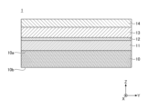
- FIG. 1 is a cross-sectional view showing a reflective mask blank according to one embodiment.
- FIG. 2 is a cross-sectional view showing a reflective mask according to one embodiment.
- FIG. 3 is a cross-sectional view showing an example of EUV light reflected by the reflective mask of FIG. 2.
- FIG. 4 is a sectional view showing a reflective mask blank according to a modified example.
- FIG. 5 is a diagram showing a TEM image of the multilayer reflective film and protective film of Example 1 in Table 1.
- FIG. 6 is an enlarged view of the area surrounded by the broken line VI in FIG.
- FIG. 7 is a diagram showing the brightness profile of FIG. 6.
- FIG. 8 is a flowchart illustrating a method for manufacturing a reflective mask blank according to one embodiment.
- FIG. 9 is a flowchart illustrating a method for manufacturing a reflective mask according to one embodiment.
- the X-axis direction, the Y-axis direction, and the Z-axis direction are directions perpendicular to each other.
- the Z-axis direction is a direction perpendicular to the first main surface 10a of the substrate 10.
- the X-axis direction is a direction perpendicular to the incident plane of EUV light (the plane including the incident light beam and the reflected light beam).
- the more the incident ray goes in the negative direction of the Z-axis the more it tilts in the positive direction of the Y-axis, and the more the reflected ray goes in the positive direction of the Z-axis, the more it tilts in the positive direction of the Y-axis. do.
- the reflective mask blank 1 includes, for example, a substrate 10, a multilayer reflective film 11, a protective film 12, an absorbing film 13, and an etching mask film 14 in this order.
- the multilayer reflective film 11, the protective film 12, the absorption film 13, and the etching mask film 14 are formed on the first main surface 10a of the substrate 10 in this order.
- the reflective mask blank 1 only needs to include at least a substrate 10, a multilayer reflective film 11, a protective film 12, and an absorbing film 13.
- the reflective mask blank 1 may further include a functional film not shown in FIG.
- the reflective mask blank 1 may have a conductive film on the side opposite to the multilayer reflective film 11 with respect to the substrate 10.
- the conductive film is formed on the second main surface 10b of the substrate 10.
- the second main surface 10b is a surface opposite to the first main surface 10a.
- the conductive film is used, for example, to attract the reflective mask 2 to an electrostatic chuck of an exposure apparatus.
- the reflective mask blank 1 may have a buffer film between the protective film 12 and the absorption film 13.
- the buffer film protects the protective film 12 from the etching gas that forms the opening pattern 13a in the absorption film 13.
- the buffer film is etched more slowly than the absorption film 13.
- the buffer film ultimately has the same opening pattern as the opening pattern 13a of the absorption film 13.
- the reflective mask 2 is manufactured using, for example, the reflective mask blank 1 shown in FIG. 1, and includes an opening pattern 13a in the absorbing film 13. Note that the etching mask film 14 shown in FIG. 1 is removed after the opening pattern 13a is formed in the absorption film 13.
- the opening pattern 13a of the absorption film 13 is transferred to a target substrate such as a semiconductor substrate. Transferring includes reducing and transferring.
- the substrate 10, multilayer reflective film 11, protective film 12, absorption film 13, and etching mask film 14 will be explained in this order.
- the substrate 10 is, for example, a glass substrate.
- the material of the substrate 10 is preferably silica glass containing TiO 2 .
- Quartz glass has a smaller coefficient of linear expansion and less dimensional change due to temperature changes than common soda lime glass.
- the quartz glass may contain 80% to 95% by weight of SiO 2 and 4% to 17% by weight of TiO 2 . When the TiO 2 content is 4% by mass to 17% by mass, the coefficient of linear expansion near room temperature is approximately zero, and almost no dimensional change occurs near room temperature.
- the quartz glass may contain a third component or impurity other than SiO 2 and TiO 2 . Note that the material of the substrate 10 may be crystallized glass with ⁇ -quartz solid solution precipitated thereon, silicon, metal, or the like.
- the substrate 10 has a first main surface 10a and a second main surface 10b opposite to the first main surface 10a.
- a multilayer reflective film 11 and the like are formed on the first main surface 10a.
- the size of the substrate 10 in plan view is, for example, 152 mm in length and 152 mm in width.
- the vertical and horizontal dimensions may be 152 mm or more.
- the first main surface 10a and the second main surface 10b have, for example, a square quality assurance area at their centers.
- the size of the quality assurance area is, for example, 142 mm in length and 142 mm in width.
- the quality assurance area of the first principal surface 10a preferably has a root mean square roughness (RMS) of 0.150 nm or less and a flatness of 100 nm or less. Moreover, it is preferable that the quality assurance area of the first principal surface 10a does not have any defects that cause phase defects.
- RMS root mean square roughness
- the multilayer reflective film 11 reflects EUV light.
- the multilayer reflective film 11 is, for example, a structure in which high refractive index layers and low refractive index layers are alternately laminated.
- the material of the high refractive index layer is, for example, silicon (Si)
- the material of the low refractive index layer is, for example, molybdenum (Mo)
- Mo/Si multilayer reflective film is used.
- each layer and the number of repeating units of each layer constituting the multilayer reflective film 11 can be appropriately selected depending on the material of each layer and the reflectance to EUV light.
- the multilayer reflective film 11 is a Mo/Si multilayer reflective film, in order to achieve a reflectance of 60% or more for EUV light with an incident angle ⁇ (see FIG. 3) of 6°, the film thickness must be 2.
- a Mo film with a thickness of 3 ⁇ 0.1 nm and a Si film with a thickness of 4.5 ⁇ 0.1 nm may be laminated so that the number of repeating units is 30 or more and 60 or less.
- the multilayer reflective film 11 preferably has a reflectance of 60% or more for EUV light with an incident angle ⁇ of 6°. The reflectance is more preferably 65% or more.
- the method for forming each layer constituting the multilayer reflective film 11 is, for example, a DC sputtering method, a magnetron sputtering method, or an ion beam sputtering method.
- a Mo/Si multilayer reflective film using the ion beam sputtering method an example of the film forming conditions for each of the Mo film and the Si film is as follows. ⁇ Si film formation conditions> Target: Si target, Sputter gas: Ar gas, Gas pressure: 0.013Pa to 0.027Pa, Ion acceleration voltage: 300V to 1500V, Film formation rate: 0.030 nm/sec to 0.300 nm/sec, Film thickness of Si film: 4.5 ⁇ 0.1 nm.
- the protective film 12 is formed between the multilayer reflective film 11 and the absorption film 13 to protect the multilayer reflective film 11.
- the protective film 12 protects the multilayer reflective film 11 from the etching gas that forms the opening pattern 13a (see FIG. 2) in the absorption film 13.
- the protective film 12 remains on the multilayer reflective film 11 without being removed during manufacturing of the reflective mask 2.
- the etching gas is, for example, a halogen-based gas, an oxygen-based gas, or a mixed gas thereof.
- the halogen gas include chlorine gas and fluorine gas.
- the chlorine-based gas is, for example, Cl 2 gas, SiCl 4 gas, CHCl 3 gas, CCl 4 gas, BCl 3 gas, or a mixed gas thereof.
- the fluorine-based gas is, for example, CF 4 gas, CHF 3 gas, SF 6 gas, BF 3 gas, XeF 2 gas, or a mixed gas thereof.
- the oxygen-based gas is O 2 gas, O 3 gas, or a mixed gas thereof.
- the oxygen-based gas is preferably used when the main component of the absorption film 13 is ruthenium (Ru).
- the ratio (ER1/ER2) of the etching rate ER1 of the absorbing film 13 by the etching gas to the etching rate ER2 of the protective film 12 by the etching gas is also referred to as selectivity.
- the selectivity ratio is preferably 10 or more, more preferably 30 or more.
- the selectivity ratio is preferably 200 or less, more preferably 100 or less.
- the protective film 12 contains Rh from 50 at% to 100 at%.
- the protective film 12 is preferably made of a single layer as shown in FIG. 1 from the viewpoint of productivity, but may be made of a plurality of layers as shown in FIG. 4 from the viewpoint of multifunctionality.
- the protective film 12 may include a lower layer 12L and an upper layer 12U.
- the lower layer 12L and the upper layer 12U are formed on the multilayer reflective film 11 in this order. In any case, it is sufficient that the protective film 12 contains 50 at % or more of Rh as a whole.
- the protective film 12 contains Rh as a main component.
- Rh instead of Ru as the main component of the protective film 12, the etching resistance of the protective film 12 can be improved.
- an oxygen-based gas is used as the etching gas (including when a mixed gas is used), the etching resistance of the protective film 12 can be improved.
- Rh instead of Ru as the main component of the protective film 12
- resistance to sulfuric acid/hydrogen peroxide can also be improved.
- the sulfuric acid peroxide solution is used for removing a resist film or cleaning the reflective mask 2, which will be described later.
- Rh instead of Ru as the main component of the protective film 12, it is possible to suppress a decrease in reflectance with respect to EUV light.
- the protective film 12 has a brightness profile peak number Np of 50 or more per 100 nm in the longitudinal direction of a grayscale image, which will be described later.
- Np brightness profile peak number
- the number Np of peaks in the brightness profile per 100 nm in the longitudinal direction of the grayscale image will also be simply referred to as the number Np of peaks.
- the grayscale image is obtained by imaging a cross section of the protective film 12 using a transmission electron microscope (TEM).
- the electron acceleration voltage of the TEM is, for example, 200 kV.
- a grayscale image has, for example, 256 gradations, a magnification of 2.5 million times, and a resolution of 0.16 nm/pixel.
- the grayscale image captured by the TEM may include a cross section of the multilayer reflective film 11 in addition to the cross section of the protective film 12, as shown in FIG.
- the grayscale image (the image of the area surrounded by the broken line VI in FIG. 5) for creating the brightness profile is a belt-like image parallel to the interface between the protective film 12 and the multilayer reflective film 11, and is located on the center line in the thickness direction of the protective film 12. It is cut out.
- the gray scale image for creating the brightness profile has a vertical dimension of 1 nm and a horizontal dimension of 74 nm.
- the vertical direction is a direction perpendicular to the interface between the protective film 12 and the multilayer reflective film 11 (Z-axis direction).
- the lateral direction is a direction parallel to the interface between the protective film 12 and the multilayer reflective film 11 (Y-axis direction or X-axis direction). Note that the lateral dimension may be 60 nm or more.
- the brightness profile is created using a function called Plot profile of ImageJ (version 1.53e) distributed by the National Institutes of Health (NIH).
- ImageJ is open source, public domain image processing software.
- the brightness of the brightness profile is output as an average value of 1 nm in the vertical direction.
- the brightness profile is smoothed by polynomial approximation using the least squares method.
- Python 3 is used and a Savitzky-Golay filter is used.
- the filter is expressed in the Python code as follows.
- z polynominal_order (order of polynomial approximation used during smoothing) x is all the luminances in the luminance profile acquired in the lateral direction from the TEM image.
- y is 11.
- z is 5.
- FIG. 7 shows an example of the brightness profile after smoothing.
- the horizontal axis represents the longitudinal position of the grayscale image
- the vertical axis represents the magnitude of brightness
- the black dot represents the position of the peak.
- the peak of the brightness profile after smoothing is calculated using scipy. signal. Detected by argrelmax. signal. The order value of argrelmax is 2.
- Np Np 0 ⁇ (100/L X0 )...(1) Calculate using.
- Np 0 is the number of peaks of the brightness profile
- L X0 is the lateral dimension (unit: nm) of the brightness profile.
- L X0 is, for example, 74 nm. Note that L X0 only needs to be 60 nm or more.
- the brightness of the image differs between the inside of the crystal and the grain boundary.
- the grain boundaries are brighter than the interior of the crystal.
- the denser the protective film 12 is, the smaller the crystal grain size, the more grain boundaries, and the larger the number of peaks Np.
- the denser the protective film 12 is, the better the etching resistance is. Therefore, the greater the number of peaks Np, the better the etching resistance.
- the number of peaks Np is preferably 50 or more, more preferably 55 or more. Further, the number of peaks Np is preferably 120 or less, more preferably 100 or less.
- the main component of the protective film 12 is Rh
- the protective film 12 is formed by the ion beam sputtering method after forming the multilayer reflective film 11 by the magnetron sputtering method
- the protective film 12 The density is low and the number of peaks Np is less than 50.
- the main component of the protective film 12 is Ru
- the denseness of the protective film 12 is high; The number of peaks Np becomes 50 or more.
- a vacuum chamber used for forming the multilayer reflective film 11 and a vacuum chamber used for forming the protective film 12 are provided separately. Therefore, after the multilayer reflective film 11 is formed and before the protective film 12 is formed, the multilayer reflective film 11 is exposed to the atmosphere, and the uppermost layer of the multilayer reflective film 11 is oxidized.
- the uppermost layer of the multilayer reflective film 11 is a layer that is in contact with the protective film 12 among the multiple layers that constitute the multilayer reflective film 11 .
- the main component of the protective film 12 is Rh, unlike the case where the main component of the protective film 12 is Ru, it is considered that when the top layer of the multilayer reflective film 11 is oxidized, the density of the protective film 12 becomes lower. It will be done.
- the inventor of the present application has demonstrated that even when the main component of the protective film 12 is Rh, the multilayer reflective film 11 and the protective film 12 are formed in this order in the same vacuum chamber. It has been found that the denseness of the protective film 12 can be improved by forming a film. In other words, even when the main component of the protective film 12 is Rh, the inventor of the present application has realized that even if the main component of the protective film 12 is Rh, by suppressing the exposure of the multilayer reflective film 11 to the atmosphere and suppressing the oxidation of the uppermost layer of the multilayer reflective film 11, the protective film 12 can be protected. It has been found that the denseness of the membrane 12 can be improved.
- the multilayer reflective film 11 has, as the uppermost layer in contact with the protective film 12, a Si film whose oxygen atom content is preferably 15 at % or less.
- the content of oxygen atoms in the Si film, which is the uppermost layer of the multilayer reflective film 11, is measured by, for example, TEM-EDX (Energy Dispersive X-ray).
- the multilayer reflective film 11 and the protective film 12 in this order in the same vacuum chamber, oxidation of the Si film that is the top layer of the multilayer reflective film 11 can be suppressed, and the O content of the Si film that is the top layer can be reduced. can be reduced to 15 at% or less.
- the O content of the Si film, which is the uppermost layer, is more preferably 10 at% or less, and still more preferably 5 at% or less.
- the pressure in the vacuum chamber it is preferable to control the pressure in the vacuum chamber to 0.035 Pa or less when forming the protective film 12. If the pressure of the vacuum chamber is 0.035 Pa or less, the degree of vacuum is high and oxidation is suppressed.
- the pressure of the vacuum chamber is more preferably 0.030 Pa or less. Moreover, the pressure of the vacuum chamber may be 0.001 Pa or more.
- the multilayer reflective film 11 and the protective film 12 are formed in the same vacuum chamber, they are formed using the same film forming method. From the viewpoint of the degree of vacuum, ion beam sputtering is suitable as the film forming method. According to the ion beam sputtering method, the vacuum chamber and the plasma source can be separated, and the degree of vacuum in the vacuum chamber can be increased.
- the number of peaks Np of the protective film 12 can be adjusted by adjusting the ion acceleration voltage.
- the energy of sputtered particles is lowered, the density of the protective film 12 is increased, and the gas barrier properties of the protective film 12 are improved.
- the number of peaks Np can be made 50 or more by setting the ion acceleration voltage to 400V or more and 800V or less.
- the number of peaks Np of the protective film 12 can be adjusted by adjusting the gas pressure of the sputtering gas (for example, Ar). .
- the gas pressure of the sputtering gas for example, Ar
- the number of peaks Np can be set to 50 or more.
- the number of peaks Np can be made 50 or more by setting the gas pressure of the sputtering gas to 0.0050 Pa or more and 0.050 Pa or less.
- the protective film 12 may contain only Rh as a metal element, or may contain at least one element X selected from Ru, Pd, Ir, Pt, Zr, Nb, Ta, and Ti in addition to Rh. It's okay.
- the protective film 12 is formed of Rh alone or a Rh compound. Rh compounds contain Rh and X. Ru, Zr, Nb, and Ti can improve the reflectance for EUV light. Pd, Ir and Pt can improve etching resistance. Ta can improve resistance to hydrogen.
- the element ratio of Rh and X is preferably 50:50 to 99:1.
- elemental ratio refers to molar ratio.
- the element ratio (Rh:X) is more preferably 70:30 to 95:5.
- the protective film 12 may contain at least one nonmetal element selected from O, N, C, and B in addition to the above-mentioned metal elements.
- the Rh compound constituting the protective film 12 may contain at least Rh and a nonmetallic element, and may further contain X.
- the thickness of the protective film 12 is preferably 1.5 nm or more and 4.0 nm or less, more preferably 2.0 nm or more and 3.5 nm or less. If the thickness of the protective film 12 is 1.5 nm or more, the etching resistance is good. Moreover, if the thickness of the protective film 12 is 4.0 nm or less, a decrease in reflectance to EUV light can be suppressed.
- the film density of the protective film 12 is preferably 10.0 g/cm 3 or more and 14.0 g/cm 3 or less. If the film density of the protective film 12 is 10.0 g/cm 3 or more, the etching resistance is good. Further, if the film density of the protective film 12 is 14.0 g/cm 3 or less, a decrease in reflectance to EUV light can be suppressed.
- the root mean square roughness RMS of the upper surface of the protective film 12, that is, the surface on which the absorption film 13 of the protective film 12 is formed, is preferably 0.300 nm or less, more preferably 0.150 nm or less. If the root mean square roughness RMS is 0.300 nm or less, the absorbing film 13 and the like can be formed smoothly on the protective film 12. Further, scattering of EUV light can be suppressed, and reflectance for EUV light can be improved.
- the root mean square roughness RMS is preferably 0.050 nm or more.
- the protective film 12 may be composed of multiple layers, and may include, for example, a lower layer 12L and an upper layer 12U.
- the lower layer 12L and the upper layer 12U are formed on the multilayer reflective film 11 in this order. That is, the lower layer 12L is provided between the upper layer 12U and the multilayer reflective film 11.
- the upper layer 12U contains Rh from 50 at% to 100 at%. Since the main component of the upper layer 12U is Rh, the following effects (A) to (C) can be obtained.
- (A) Etching resistance of the absorption film 13 can be improved. In particular, when an oxygen-based gas is used as the etching gas, the etching resistance of the protective film 12 can be improved.
- C) The reflectance for EUV light can be improved.
- the upper layer 12U may contain only Rh as a metal element, or may contain at least one element X selected from Ru, Pd, Ir, Pt, Zr, Nb, Ta, and Ti in addition to Rh. Good too.
- the upper layer 12U is formed of Rh alone or a Rh compound. Rh compounds contain Rh and X.
- the elemental ratio of Rh and X (Rh:X) in the upper layer 12U is preferably 99:1 to 1:1, more preferably 70:30 to 95:5.
- the upper layer 12U may contain at least one nonmetal element selected from O, N, C, and B in addition to the above metal elements.
- the Rh compound constituting the upper layer 12U may contain at least Rh and a nonmetallic element, and may further contain X.
- the thickness of the upper layer 12U is preferably 0.1 nm or more and 4.0 nm or less, more preferably 0.2 nm or more and 3.5 nm or less, still more preferably 0.5 nm or more and 3.0 nm or less, and particularly preferably It is 1.0 nm or more and 2.5 nm or less. If the thickness of the upper layer 12U is 0.1 nm or more, the etching resistance is good. Further, if the thickness of the upper layer 12U is 4.0 nm or less, a decrease in reflectance to EUV light can be suppressed.
- the lower layer 12L preferably contains Ru, Pd, Ir, Pt, Zr, Nb, Ta, or Ti in an amount of 50 at% or more and 100 at% or less. That is, the main component of the lower layer 12L is a metal element other than Rh, preferably Ru, Pd, Ir, Pt, Zr, Nb, Ta, or Ti. That is, the lower layer 12L is formed of the above-mentioned metal elements alone or in combination. Ru, Zr, Nb, and Ti can improve the reflectance for EUV light. Pd, Ir, and Pt can improve the etching resistance of the protective film 12. Ta can improve resistance to hydrogen. The main component of the lower layer 12L is more preferably Ru.
- the lower layer 12L may contain at least one nonmetal element selected from O, N, C, and B in addition to the above metal elements.
- the metal compound constituting the lower layer 12L may contain at least the above metal elements and nonmetal elements.
- the thickness of the lower layer 12L is preferably 0.5 nm or more and 2.0 nm or less, more preferably 0.5 nm or more and 1.5 nm or less.
- the thickness of the lower layer 12L containing a metal element other than Rh as a main component is preferably thinner than the thickness of the upper layer 12U containing Rh as a main component.
- the protective film 12 as a whole contains 50 at % or more of Rh, and the thickness of the lower layer 12L may be thicker than the thickness of the upper layer 12U.
- an example of film forming conditions is as follows. ⁇ Film formation conditions for Ru film (lower layer)> Target: Ru target, Sputter gas: Ar gas, Gas pressure: 0.010Pa to 0.020Pa, Ion acceleration voltage: 300V to 1500V, Film formation rate: 0.010 nm/sec to 0.100 nm/sec, Thickness of Ru film: 0.5 nm to 2.0 nm.
- Rh film As the upper layer 12U using the ion beam sputtering method, an example of film forming conditions is as follows. ⁇ Film formation conditions for Rh film (upper layer)> Target: Rh target, Sputter gas: Ar gas, Gas pressure: 0.010Pa to 0.035Pa, Ion acceleration voltage: 300V to 1500V, Film formation rate: 0.010 nm/sec to 0.100 nm/sec, Rh film thickness: 0.5 nm to 4.0 nm.
- the absorption film 13 is a film on which an opening pattern 13a is formed.
- the opening pattern 13a is not formed in the manufacturing process of the reflective mask blank 1, but is formed in the manufacturing process of the reflective mask 2.
- the absorption film 13 may not only absorb EUV light but also shift the phase of EUV light. That is, the absorption film 13 may be a phase shift film.
- the phase shift film shifts the phase of the second EUV light L2 with respect to the first EUV light L1 shown in FIG.
- the first EUV light L1 is light that passes through the opening pattern 13a without passing through the absorption film 13, is reflected by the multilayer reflective film 11, and passes through the opening pattern 13a again without passing through the absorption film 13.
- the second EUV light L2 is light that is transmitted through the absorption film 13 while being absorbed by the absorption film 13, reflected by the multilayer reflection film 11, and transmitted through the absorption film 13 while being absorbed by the absorption film 13 again.
- the phase difference ( ⁇ 0) between the first EUV light L1 and the second EUV light L2 is, for example, 170° to 250°.
- the phase of the first EUV light L1 may lead or lag the phase of the second EUV light L2.
- the absorption film 13 improves the contrast of the transferred image by utilizing the interference between the first EUV light L1 and the second EUV light L2.
- the transferred image is an image obtained by transferring the opening pattern 13a of the absorption film 13 onto the target substrate.
- the shadowing effect is caused by the fact that the incident angle ⁇ of the EUV light is not 0° (for example, 6°), and a region is created near the sidewall of the aperture pattern 13a where the sidewall blocks the EUV light, resulting in a transferred image. This refers to the occurrence of positional or dimensional deviations.
- it is effective to reduce the height of the side wall of the opening pattern 13a, and it is effective to reduce the thickness of the absorption film 13.
- the thickness of the absorption film 13 is, for example, 60 nm or less, preferably 50 nm or less, in order to reduce the shadowing effect.
- the thickness of the absorption film 13 is preferably 20 nm or more, more preferably 30 nm or more in order to ensure a phase difference between the first EUV light L1 and the second EUV light L2.
- the absorption film 13 preferably contains at least one metal element selected from Ru, Ta, Cr, Nb, Pt, Ir, Re, W, Mn, Au, Si, and Al. Since these metal elements have a relatively small refractive index, the thickness of the phase shift film can be reduced while ensuring a phase difference. It is preferable that the absorption film 13 contains Ru among the above metal elements.
- the absorption film 13 is formed of a single substance or a compound of the above-mentioned metal elements.
- the absorption film 13 contains at least one nonmetal element selected from O, N, C, and B in addition to the above-mentioned metal elements.
- the compound constituting the absorption film 13 may contain the above metal elements and nonmetal elements. By adding a non-metal element to the metal element, crystallization of the absorption film 13 can be suppressed, and the roughness of the sidewall of the opening pattern 13a can be reduced.
- the absorption film 13 preferably contains oxygen as a nonmetallic element, and more preferably contains oxygen and nitrogen.
- the refractive index n of the absorption film 13 is preferably 0.930 or less, more preferably 0.920 or less, still more preferably 0.910 or less, and particularly preferably 0.90 or less. Further, the refractive index n is preferably 0.885 or more. In this specification, the refractive index is the refractive index for light with a wavelength of 13.5 nm.
- the extinction coefficient k of the absorption film 13 is preferably 0.015 or more, more preferably 0.020 or more. Further, the extinction coefficient k is preferably 0.065 or less. In this specification, the extinction coefficient is an extinction coefficient for light with a wavelength of 13.5 nm.
- the absorption film 13 preferably has an etching rate of 0 nm/min to 0.05 nm/min using sulfuric acid/hydrogen. If the etching rate of the absorption film 13 by sulfuric acid peroxide is 0.05 nm/min or less, damage to the absorption film 13 can be suppressed during cleaning.
- a method for forming the absorption film 13 is, for example, a DC sputtering method, a magnetron sputtering method, an ion beam sputtering method, or a reactive sputtering method.
- the oxygen content of the absorption film 13 can be controlled by the content of O 2 gas in the sputtering gas.
- the nitrogen content of the absorption film 13 can be controlled by the content of N 2 gas in the sputtering gas.
- RuN film formation conditions ⁇ RuN film formation conditions>
- Target Ru target
- Sputtering gas mixed gas of Ar gas and N2 gas
- Gas pressure 0.05Pa to 0.40Pa
- Input power 100W to 300W
- Film formation rate 0.010 nm/sec to 0.030 nm/sec
- Film thickness 20nm to 60nm.
- the etching mask film 14 is formed on the side opposite to the protective film 12 with respect to the absorption film 13, and is used to form the opening pattern 13a in the absorption film 13.
- a resist film (not shown) is provided on the etching mask film 14.
- first a first opening pattern is formed in the resist film, then a second opening pattern is formed in the etching mask film 14 using the first opening pattern, and then a second opening pattern is formed in the etching mask film 14.
- a third opening pattern 13a is formed in the absorption film 13 using the following method.
- the first aperture pattern, the second aperture pattern, and the third aperture pattern 13a have the same dimensions and the same shape in a plan view (as viewed in the Z-axis direction).
- the etching mask film 14 allows the resist film to be made thinner.
- the etching mask film 14 preferably contains at least one metal element selected from Cr, Nb, Ti, Mo, Ta, and Si.
- the etching mask film 14 is formed of the above-mentioned metal elements alone or in combination.
- the etching mask film 14 may contain at least one non-metal element selected from O, N, C, and B in addition to the above-mentioned metal elements.
- the compound constituting the etching mask film 14 may contain the above metal elements and nonmetal elements.
- the thickness of the etching mask film 14 is preferably 2 nm or more and 30 nm or less, more preferably 2 nm or more and 25 nm or less, and still more preferably 2 nm or more and 10 nm or less.
- a method for forming the etching mask film 14 is, for example, a DC sputtering method, a magnetron sputtering method, or an ion beam sputtering method.
- the method for manufacturing the reflective mask blank 1 includes steps S101 to S105 shown in FIG. 8, for example.
- step S101 the substrate 10 is prepared.
- step S102 a multilayer reflective film 11 is formed on the first main surface 10a of the substrate 10.
- step S103 a protective film 12 is formed on the multilayer reflective film 11.
- step S104 the absorbing film 13 is formed on the protective film 12.
- step S105 an etching mask film 14 is formed on the absorption film 13.
- the method for manufacturing the reflective mask blank 1 only needs to include at least steps S101 to S104.
- the method for manufacturing the reflective mask blank 1 may further include a step of forming a functional film not shown in FIG.
- the method for manufacturing the reflective mask 2 includes steps S201 to S204 shown in FIG.
- step S201 a reflective mask blank 1 is prepared.
- step S202 the etching mask film 14 is processed.
- a resist film (not shown) is provided on the etching mask film 14.
- step S203 a third opening pattern 13a is formed in the absorption film 13 using the second opening pattern.
- step S203 the absorption film 13 is etched using an etching gas.
- the resist film and etching mask film 14 are removed.
- step S204 removal of the etching mask film 14
- step S203 etching the absorption film 13
- Examples 1 to 2 and 4 below are examples, and Examples 3 and 5 are comparative examples.
- Example 1 a reflective mask blank including a substrate, a multilayer reflective film, a protective film, and an absorbing film in this order was produced.
- a substrate a SiO 2 -TiO 2 -based glass substrate (outer size: 6 inches (152 mm) square, thickness: 6.3 mm) was prepared.
- This glass substrate has a thermal expansion coefficient of 0.02 ⁇ 10 ⁇ 7 /°C at 20°C, a Young's modulus of 67 GPa, a Poisson's ratio of 0.17, and a specific stiffness of 3.07 ⁇ 10 7 m. 2 / s2 .
- the quality assurance area of the first main surface of the substrate had a root mean square roughness (RMS) of 0.150 nm or less and a flatness of 100 nm or less by polishing.
- RMS root mean square roughness
- a Cr film with a thickness of 100 nm was formed on the second main surface of the substrate using a magnetron sputtering method.
- the sheet resistance of the Cr film was 100 ⁇ / ⁇ .
- a Mo/Si multilayer reflective film was formed as the multilayer reflective film.
- the Mo/Si multilayer reflective film was formed by repeating 40 times of forming a Si film (4.5 nm thick) and a Mo film (2.3 nm thick) using an ion beam sputtering method.
- the total film thickness of the Mo/Si multilayer reflective film was 272 nm ((4.5 nm+2.3 nm) ⁇ 40).
- a Si film was used as the top layer to prevent oxidation of the Mo film. Generally, Mo films are more easily oxidized than Si films.
- Si film formation conditions Si target (boron doped), Sputter gas: Ar gas, Gas pressure: 0.020Pa, Ion acceleration voltage: 700V, Film formation rate: 0.077 nm/sec, Film thickness: 4.5 nm.
- Mo target Si target (boron doped)
- Sputter gas Ar gas
- Gas pressure: 0.020Pa Ion acceleration voltage: 700V
- Film formation rate: 0.064 nm/sec Film thickness: 2.3 nm.
- a Rh film (single layer) was formed.
- the Rh film was formed using an ion beam sputtering method.
- the multilayer reflective film and the protective film were formed in this order in the same vacuum chamber. After the multilayer reflective film was formed and before the protective film was formed, the multilayer reflective film was not exposed to the atmosphere, and the top layer of the multilayer reflective film was not oxidized.
- the conditions for forming the Rh film were as follows. ⁇ Film formation conditions for Rh film (single layer)> Target: Rh target, Sputter gas: Ar gas, Gas pressure: 0.027Pa, Ion acceleration voltage: 600V, Film formation rate: 0.077 nm/sec, Film thickness: 3.0 nm.
- a RuN film (thickness: 39 nm) was formed as the absorption film.
- the RuN film was formed using a reactive sputtering method.
- the conditions for forming the RuN film were as follows. ⁇ RuN film formation conditions> Target: Ru target, Sputtering gas: mixed gas of Ar gas and N2 gas, Volume ratio of N2 gas in sputtering gas ( N2 /(Ar+ N2 )): 0.5, Gas pressure: 0.20Pa, Input power: 200W, Film formation rate: 0.017 nm/sec, Film thickness: 39nm.
- a reflective mask blank was obtained using the above procedure.
- the O content of the Si film, which is the uppermost layer of the multilayer reflective film, the peak number Np of the protective film, and the etching resistance of the protective film were measured before the absorption film was formed.
- the O content of the Si film which is the top layer of the multilayer reflective film, was measured using TEM-EDX (manufactured by JEOL Ltd., trade name ARM200F) before performing the etching test described below.
- the lower limit of measurement was 4 at%.
- the peak number Np of the protective film was measured using a TEM (trade name: ARM200F, manufactured by JEOL Ltd.) before performing the following etching test. The measurement procedure was as described above. It is considered that the larger the number of peaks Np is, the denser the protective film is.
- the etching test was conducted using an ICP (inductively coupled) plasma etching device.
- the specific etching conditions were as follows. ⁇ Etching conditions> ICP antenna bias: 200W, Substrate bias: 550W, Etching time: 15sec, Trigger pressure: 3.5 ⁇ 10 2 Pa, Etching pressure: 3.0 ⁇ 10 ⁇ 1 Pa, Etching gas: mixed gas of Cl2 gas and O2 gas, Gas flow rate (Cl 2 gas/O 2 gas): 10 sccm/10 sccm.
- the etching resistance of the protective film was evaluated by the amount of etching gas permeation, that is, the amount of increase in chlorine atoms or oxygen atoms in the multilayer reflective film.
- the multilayer reflective coating is free of chlorine atoms. Therefore, after the etching test, a line profile of the chlorine atom content (unit: at%) in the depth direction (negative Z-axis direction in FIG. 5) was obtained using TEM-EDX, and the maximum value of the line profile was obtained. TClmax was determined. The smaller T Clmax is, the more difficult it is for chlorine atoms to pass through the protective film, and the better the etching resistance of the protective film is.
- the multilayer reflective film may contain oxygen atoms.
- a multilayer reflective film can be oxidized during film formation. Therefore, before and after the etching test, line profiles of the oxygen atom content (unit: at%) in the depth direction (negative Z-axis direction in Figure 5) were obtained using TEM-EDX, and the two line profiles were The maximum value T Omax of the difference (>0) was determined. The smaller T Omax is, the more difficult it is for oxygen atoms to pass through the protective film, and the better the etching resistance of the protective film is.
- Example 2 an EUV mask blank was produced under the same conditions as in Example 1, except that a Ru film (lower layer) and a Rh film (upper layer) were formed as protective films under the following conditions.
- the multilayer reflective film and the protective film were formed in this order in the same vacuum chamber. After the multilayer reflective film was formed and before the protective film was formed, the multilayer reflective film was not exposed to the atmosphere, and the top layer of the multilayer reflective film was not oxidized. Furthermore, in Example 2, the peak number Np of the protective film and the etching resistance of the protective film were measured using the same procedure as in Example 1.
- Example 3 an EUV mask blank was produced under the same conditions as in Example 1, except that a Rh film (single layer) was formed as a protective film under the following conditions.
- the Rh film was formed by DC magnetron sputtering. Therefore, the multilayer reflective film and the protective film were formed in different vacuum chambers. After forming the multilayer reflective film and before forming the protective film, the multilayer reflective film was exposed to the atmosphere, and the uppermost layer of the multilayer reflective film was oxidized. Furthermore, in Example 3, the peak number Np of the protective film and the etching resistance of the protective film were measured using the same procedure as in Example 1.
- Rh target Rh target
- Sputter gas Ar gas
- Gas pressure 0.130Pa
- Input power 300W
- Film formation rate 0.090 nm/sec
- Film thickness 2.5 nm.
- Example 4 In Example 4, a Rh film (single layer) was formed as a protective film. An EUV mask blank was produced under the same conditions as in Example 1 except for the thickness of the Rh film (single layer). The multilayer reflective film and the protective film were formed in this order in the same vacuum chamber. After the multilayer reflective film was formed and before the protective film was formed, the multilayer reflective film was not exposed to the atmosphere, and the top layer of the multilayer reflective film was not oxidized. Furthermore, in Example 4, the peak number Np of the protective film and the etching resistance of the protective film were measured using the same procedure as in Example 1.
- Rh target Rh target
- Sputter gas Ar gas
- Gas pressure 0.027Pa
- Ion acceleration voltage 600V
- Film formation rate 0.077 nm/sec
- Film thickness 2.5 nm.
- Example 5 an EUV mask blank was produced under the same conditions as in Example 1, except that a Ru film (lower layer) and a Rh film (upper layer) were formed as protective films under the following conditions.
- the multilayer reflective film and the protective film were formed in this order in a vacuum chamber. After the multilayer reflective film was formed and before the Ru film (lower layer) was formed as a protective film, the multilayer reflective film was not exposed to the atmosphere. After the Ru film (lower layer) was formed, the Ru film (lower layer) was exposed to the atmosphere, and the uppermost layer of the multilayer reflective film was oxidized. After exposure to the atmosphere, a Rh film (upper layer) was formed on the Ru film (lower layer).
- Example 5 the peak number Np of the protective film and the etching resistance of the protective film were measured using the same procedure as in Example 1.
- Table 1 shows the results of Examples 1 to 5.
- Example 1 unlike Examples 3 and 5, in Examples 1 to 2 and 4, the multilayer reflective film and the protective film were formed successively without being exposed to the atmosphere, so the uppermost layer of the multilayer reflective film The Si film was not oxidized, and the O content of the Si film was 15 at % or less. Further, in Examples 1 to 2 and 4, unlike Examples 3 and 5, the peak number Np of the protective film was 50 or more, and T Clmax and T Omax were smaller than in Example 3. Furthermore, in Examples 1 and 2, the root mean square roughness RMS of the surface of the protective film was smaller than in Example 3.
Landscapes
- Physics & Mathematics (AREA)
- General Physics & Mathematics (AREA)
- Preparing Plates And Mask In Photomechanical Process (AREA)
- Exposure And Positioning Against Photoresist Photosensitive Materials (AREA)
- Engineering & Computer Science (AREA)
- Plasma & Fusion (AREA)
Priority Applications (9)
| Application Number | Priority Date | Filing Date | Title |
|---|---|---|---|
| JP2023548742A JP7367902B1 (ja) | 2022-04-01 | 2023-03-27 | 反射型マスクブランク、反射型マスク、反射型マスクブランクの製造方法、および反射型マスクの製造方法 |
| KR1020257034808A KR20250153884A (ko) | 2022-04-01 | 2023-03-27 | 반사형 마스크 블랭크, 반사형 마스크, 반사형 마스크 블랭크의 제조 방법 및 반사형 마스크의 제조 방법 |
| KR1020237035081A KR102685023B1 (ko) | 2022-04-01 | 2023-03-27 | 반사형 마스크 블랭크, 반사형 마스크, 반사형 마스크 블랭크의 제조 방법 및 반사형 마스크의 제조 방법 |
| KR1020247023066A KR102882943B1 (ko) | 2022-04-01 | 2023-03-27 | 반사형 마스크 블랭크, 반사형 마스크, 반사형 마스크 블랭크의 제조 방법 및 반사형 마스크의 제조 방법 |
| JP2023172712A JP7529119B2 (ja) | 2022-04-01 | 2023-10-04 | 反射型マスクブランク、反射型マスク、および反射型マスクブランクの製造方法 |
| US18/382,356 US12001133B2 (en) | 2022-04-01 | 2023-10-20 | Reflective mask blank, reflective mask, method of manufacturing reflective mask blank, and method of manufacturing reflective mask |
| US18/648,522 US12306530B2 (en) | 2022-04-01 | 2024-04-29 | Reflective mask blank, reflective mask, method of manufacturing reflective mask blank, and method of manufacturing reflective mask |
| JP2024110123A JP2024133671A (ja) | 2022-04-01 | 2024-07-09 | 反射型マスクブランク、反射型マスク、反射型マスクブランクの製造方法、および反射型マスクの製造方法 |
| US19/096,241 US20250251658A1 (en) | 2022-04-01 | 2025-03-31 | Reflective mask blank, reflective mask, method of manufacturing reflective mask blank, and method of manufacturing reflective mask |
Applications Claiming Priority (2)
| Application Number | Priority Date | Filing Date | Title |
|---|---|---|---|
| JP2022061684 | 2022-04-01 | ||
| JP2022-061684 | 2022-04-01 |
Related Child Applications (1)
| Application Number | Title | Priority Date | Filing Date |
|---|---|---|---|
| US18/382,356 Continuation US12001133B2 (en) | 2022-04-01 | 2023-10-20 | Reflective mask blank, reflective mask, method of manufacturing reflective mask blank, and method of manufacturing reflective mask |
Publications (1)
| Publication Number | Publication Date |
|---|---|
| WO2023190360A1 true WO2023190360A1 (ja) | 2023-10-05 |
Family
ID=88202236
Family Applications (1)
| Application Number | Title | Priority Date | Filing Date |
|---|---|---|---|
| PCT/JP2023/012236 Ceased WO2023190360A1 (ja) | 2022-04-01 | 2023-03-27 | 反射型マスクブランク、反射型マスク、反射型マスクブランクの製造方法、および反射型マスクの製造方法 |
Country Status (5)
| Country | Link |
|---|---|
| US (3) | US12001133B2 (https=) |
| JP (3) | JP7367902B1 (https=) |
| KR (3) | KR102882943B1 (https=) |
| TW (3) | TW202544547A (https=) |
| WO (1) | WO2023190360A1 (https=) |
Cited By (3)
| Publication number | Priority date | Publication date | Assignee | Title |
|---|---|---|---|---|
| JP2025064153A (ja) * | 2023-10-05 | 2025-04-17 | レーザーテック株式会社 | 画像処理装置、検査装置、画像処理方法及び検査方法 |
| JPWO2025079375A1 (https=) * | 2023-10-10 | 2025-04-17 | ||
| WO2025115587A1 (ja) * | 2023-11-29 | 2025-06-05 | Agc株式会社 | 反射型マスクブランク、反射型マスク、反射型マスクブランクの製造方法、及び反射型マスクの製造方法 |
Families Citing this family (1)
| Publication number | Priority date | Publication date | Assignee | Title |
|---|---|---|---|---|
| TW202548405A (zh) * | 2024-06-03 | 2025-12-16 | 日商Agc股份有限公司 | 反射型光罩基底、反射型光罩及反射型光罩之製造方法 |
Citations (4)
| Publication number | Priority date | Publication date | Assignee | Title |
|---|---|---|---|---|
| JP2006283053A (ja) * | 2005-03-31 | 2006-10-19 | Hoya Corp | スパッタリングターゲット、多層反射膜付き基板の製造方法、及び反射型マスクブランクの製造方法、並びに反射型マスクの製造方法 |
| JP2012129520A (ja) * | 2010-12-14 | 2012-07-05 | Asahi Glass Co Ltd | Euvリソグラフィ用反射型マスクブランクスの製造方法、および該マスクブランクス用の機能膜付基板の製造方法 |
| JP2015073013A (ja) * | 2013-10-03 | 2015-04-16 | 旭硝子株式会社 | Euvリソグラフィ用反射型マスクブランクの製造方法 |
| JP2021184108A (ja) * | 2020-03-27 | 2021-12-02 | Hoya株式会社 | 多層反射膜付き基板、反射型マスクブランク、反射型マスク、及び半導体デバイスの製造方法 |
Family Cites Families (15)
| Publication number | Priority date | Publication date | Assignee | Title |
|---|---|---|---|---|
| US6664554B2 (en) | 2001-01-03 | 2003-12-16 | Euv Llc | Self-cleaning optic for extreme ultraviolet lithography |
| US20030008148A1 (en) | 2001-07-03 | 2003-01-09 | Sasa Bajt | Optimized capping layers for EUV multilayers |
| US20060237303A1 (en) | 2005-03-31 | 2006-10-26 | Hoya Corporation | Sputtering target, method of manufacturing a multilayer reflective film coated substrate, method of manufacturing a reflective mask blank, and method of manufacturing a reflective mask |
| DE102012222466A1 (de) * | 2012-12-06 | 2014-06-12 | Carl Zeiss Smt Gmbh | Reflektives optisches Element für die EUV-Lithographie |
| JP6377361B2 (ja) | 2013-02-11 | 2018-08-22 | Hoya株式会社 | 多層反射膜付き基板及びその製造方法、反射型マスクブランクの製造方法、反射型マスクの製造方法、並びに半導体装置の製造方法 |
| JP6861095B2 (ja) * | 2017-03-03 | 2021-04-21 | Hoya株式会社 | 反射型マスクブランク、反射型マスク及び半導体装置の製造方法 |
| JP6845122B2 (ja) * | 2017-11-27 | 2021-03-17 | Hoya株式会社 | 反射型マスクブランク、反射型マスク及びその製造方法、並びに半導体装置の製造方法 |
| KR102402767B1 (ko) * | 2017-12-21 | 2022-05-26 | 삼성전자주식회사 | 극자외선 마스크 블랭크, 극자외선 마스크 블랭크를 이용하여 제조된 포토마스크, 포토마스크를 이용한 리소그래피 장치 및 포토마스크를 이용한 반도체 장치 제조 방법 |
| WO2020184473A1 (ja) * | 2019-03-13 | 2020-09-17 | Hoya株式会社 | 反射型マスクブランク、反射型マスク及びその製造方法、並びに半導体装置の製造方法 |
| US20210096456A1 (en) | 2019-09-30 | 2021-04-01 | Hoya Corporation | Multilayered-reflective-film-provided substrate, reflective mask blank, reflective mask, method of manufacturing reflective mask, and method of manufacturing semiconductor device |
| JP7587378B2 (ja) * | 2019-09-30 | 2024-11-20 | Hoya株式会社 | 多層反射膜付き基板、反射型マスクブランク、反射型マスク及びその製造方法、並びに半導体装置の製造方法 |
| JP7475154B2 (ja) * | 2020-02-13 | 2024-04-26 | Hoya株式会社 | 反射型マスクブランク、反射型マスク、導電膜付き基板、及び半導体装置の製造方法 |
| JP6929983B1 (ja) * | 2020-03-10 | 2021-09-01 | Hoya株式会社 | 反射型マスクブランクおよび反射型マスク、並びに半導体デバイスの製造方法 |
| JP7679357B2 (ja) * | 2020-03-30 | 2025-05-19 | Hoya株式会社 | 多層反射膜付き基板、反射型マスクブランク、反射型マスク、及び半導体装置の製造方法 |
| JP7318607B2 (ja) * | 2020-07-28 | 2023-08-01 | Agc株式会社 | Euvリソグラフィ用反射型マスクブランク、euvリソグラフィ用反射型マスク、およびそれらの製造方法 |
-
2023
- 2023-03-27 KR KR1020247023066A patent/KR102882943B1/ko active Active
- 2023-03-27 KR KR1020237035081A patent/KR102685023B1/ko active Active
- 2023-03-27 WO PCT/JP2023/012236 patent/WO2023190360A1/ja not_active Ceased
- 2023-03-27 JP JP2023548742A patent/JP7367902B1/ja active Active
- 2023-03-27 KR KR1020257034808A patent/KR20250153884A/ko active Pending
- 2023-03-29 TW TW114129628A patent/TW202544547A/zh unknown
- 2023-03-29 TW TW112111880A patent/TWI856588B/zh active
- 2023-03-29 TW TW113131113A patent/TWI896295B/zh active
- 2023-10-04 JP JP2023172712A patent/JP7529119B2/ja active Active
- 2023-10-20 US US18/382,356 patent/US12001133B2/en active Active
-
2024
- 2024-04-29 US US18/648,522 patent/US12306530B2/en active Active
- 2024-07-09 JP JP2024110123A patent/JP2024133671A/ja active Pending
-
2025
- 2025-03-31 US US19/096,241 patent/US20250251658A1/en active Pending
Patent Citations (4)
| Publication number | Priority date | Publication date | Assignee | Title |
|---|---|---|---|---|
| JP2006283053A (ja) * | 2005-03-31 | 2006-10-19 | Hoya Corp | スパッタリングターゲット、多層反射膜付き基板の製造方法、及び反射型マスクブランクの製造方法、並びに反射型マスクの製造方法 |
| JP2012129520A (ja) * | 2010-12-14 | 2012-07-05 | Asahi Glass Co Ltd | Euvリソグラフィ用反射型マスクブランクスの製造方法、および該マスクブランクス用の機能膜付基板の製造方法 |
| JP2015073013A (ja) * | 2013-10-03 | 2015-04-16 | 旭硝子株式会社 | Euvリソグラフィ用反射型マスクブランクの製造方法 |
| JP2021184108A (ja) * | 2020-03-27 | 2021-12-02 | Hoya株式会社 | 多層反射膜付き基板、反射型マスクブランク、反射型マスク、及び半導体デバイスの製造方法 |
Cited By (6)
| Publication number | Priority date | Publication date | Assignee | Title |
|---|---|---|---|---|
| JP2025064153A (ja) * | 2023-10-05 | 2025-04-17 | レーザーテック株式会社 | 画像処理装置、検査装置、画像処理方法及び検査方法 |
| JP7731951B2 (ja) | 2023-10-05 | 2025-09-01 | レーザーテック株式会社 | 画像処理装置、検査装置、画像処理方法及び検査方法 |
| JPWO2025079375A1 (https=) * | 2023-10-10 | 2025-04-17 | ||
| WO2025079375A1 (ja) * | 2023-10-10 | 2025-04-17 | Agc株式会社 | 反射型マスクブランク、反射型マスク、反射型マスクブランクの製造方法、及び反射型マスクの製造方法 |
| WO2025115587A1 (ja) * | 2023-11-29 | 2025-06-05 | Agc株式会社 | 反射型マスクブランク、反射型マスク、反射型マスクブランクの製造方法、及び反射型マスクの製造方法 |
| JP7747246B1 (ja) * | 2023-11-29 | 2025-10-01 | Agc株式会社 | 反射型マスクブランク、反射型マスク、反射型マスクブランクの製造方法、及び反射型マスクの製造方法 |
Also Published As
| Publication number | Publication date |
|---|---|
| US12306530B2 (en) | 2025-05-20 |
| JP2024133671A (ja) | 2024-10-02 |
| US12001133B2 (en) | 2024-06-04 |
| TW202544547A (zh) | 2025-11-16 |
| US20250251658A1 (en) | 2025-08-07 |
| TWI856588B (zh) | 2024-09-21 |
| KR20230156410A (ko) | 2023-11-14 |
| US20240280890A1 (en) | 2024-08-22 |
| JPWO2023190360A1 (https=) | 2023-10-05 |
| JP2023171930A (ja) | 2023-12-05 |
| KR102882943B1 (ko) | 2025-11-07 |
| JP7367902B1 (ja) | 2023-10-24 |
| TWI896295B (zh) | 2025-09-01 |
| US20240045320A1 (en) | 2024-02-08 |
| KR20250153884A (ko) | 2025-10-27 |
| KR20240115334A (ko) | 2024-07-25 |
| JP7529119B2 (ja) | 2024-08-06 |
| TW202447329A (zh) | 2024-12-01 |
| TW202403432A (zh) | 2024-01-16 |
| KR102685023B1 (ko) | 2024-07-16 |
Similar Documents
| Publication | Publication Date | Title |
|---|---|---|
| JP7367902B1 (ja) | 反射型マスクブランク、反射型マスク、反射型マスクブランクの製造方法、および反射型マスクの製造方法 | |
| JP7315123B1 (ja) | 反射型マスクブランク、反射型マスク、反射型マスクブランクの製造方法、及び反射型マスクの製造方法 | |
| JPWO2015037564A1 (ja) | 多層反射膜付き基板、euvリソグラフィー用反射型マスクブランク、euvリソグラフィー用反射型マスク及びその製造方法、並びに半導体装置の製造方法 | |
| JP7392236B1 (ja) | 反射型マスクブランク、反射型マスク、反射型マスクブランクの製造方法、および反射型マスクの製造方法 | |
| JP2026069718A (ja) | 反射型マスクブランクおよび反射型マスク | |
| JP7416342B1 (ja) | 反射型マスクブランク、反射型マスク、反射型マスクブランクの製造方法、および反射型マスクの製造方法 | |
| TW202309646A (zh) | 反射型光罩基底、反射型光罩、反射型光罩基底之製造方法、及反射型光罩之製造方法 | |
| JP2024156304A (ja) | 反射型マスクブランク、反射型マスクブランクの製造方法、及び反射型マスクの製造方法 | |
| WO2024009809A1 (ja) | 反射型マスクブランク、反射型マスク、反射型マスクブランクの製造方法、および反射型マスクの製造方法 | |
| JP2025037417A (ja) | 反射型マスクブランク、反射型マスク、反射型マスクブランクの製造方法、及び反射型マスクの製造方法 | |
| WO2024225163A1 (ja) | 反射型マスクブランク、反射型マスクブランクの製造方法、及び反射型マスクの製造方法 | |
| JP2024135499A (ja) | 反射型マスクブランク、反射型マスク、反射型マスクブランクの製造方法、及び反射型マスクの製造方法 |
Legal Events
| Date | Code | Title | Description |
|---|---|---|---|
| WWE | Wipo information: entry into national phase |
Ref document number: 2023548742 Country of ref document: JP |
|
| ENP | Entry into the national phase |
Ref document number: 20237035081 Country of ref document: KR Kind code of ref document: A |
|
| WWE | Wipo information: entry into national phase |
Ref document number: 1020237035081 Country of ref document: KR |
|
| 121 | Ep: the epo has been informed by wipo that ep was designated in this application |
Ref document number: 23780370 Country of ref document: EP Kind code of ref document: A1 |
|
| NENP | Non-entry into the national phase |
Ref country code: DE |
|
| 122 | Ep: pct application non-entry in european phase |
Ref document number: 23780370 Country of ref document: EP Kind code of ref document: A1 |
|
| WWD | Wipo information: divisional of initial pct application |
Ref document number: 1020257034808 Country of ref document: KR |
|
| WWP | Wipo information: published in national office |
Ref document number: 1020257034808 Country of ref document: KR |