WO2023190321A1 - 熱伝導性フィルム状接着剤用組成物及び熱伝導性フィルム状接着剤、並びに、熱伝導性フィルム状接着剤を用いた半導体パッケージ及びその製造方法 - Google Patents
熱伝導性フィルム状接着剤用組成物及び熱伝導性フィルム状接着剤、並びに、熱伝導性フィルム状接着剤を用いた半導体パッケージ及びその製造方法 Download PDFInfo
- Publication number
- WO2023190321A1 WO2023190321A1 PCT/JP2023/012170 JP2023012170W WO2023190321A1 WO 2023190321 A1 WO2023190321 A1 WO 2023190321A1 JP 2023012170 W JP2023012170 W JP 2023012170W WO 2023190321 A1 WO2023190321 A1 WO 2023190321A1
- Authority
- WO
- WIPO (PCT)
- Prior art keywords
- adhesive
- thermally conductive
- silane coupling
- conductive film
- film
- Prior art date
- Legal status (The legal status is an assumption and is not a legal conclusion. Google has not performed a legal analysis and makes no representation as to the accuracy of the status listed.)
- Ceased
Links
Images


Classifications
-
- C—CHEMISTRY; METALLURGY
- C09—DYES; PAINTS; POLISHES; NATURAL RESINS; ADHESIVES; COMPOSITIONS NOT OTHERWISE PROVIDED FOR; APPLICATIONS OF MATERIALS NOT OTHERWISE PROVIDED FOR
- C09J—ADHESIVES; NON-MECHANICAL ASPECTS OF ADHESIVE PROCESSES IN GENERAL; ADHESIVE PROCESSES NOT PROVIDED FOR ELSEWHERE; USE OF MATERIALS AS ADHESIVES
- C09J163/00—Adhesives based on epoxy resins; Adhesives based on derivatives of epoxy resins
-
- C—CHEMISTRY; METALLURGY
- C08—ORGANIC MACROMOLECULAR COMPOUNDS; THEIR PREPARATION OR CHEMICAL WORKING-UP; COMPOSITIONS BASED THEREON
- C08K—Use of inorganic or non-macromolecular organic substances as compounding ingredients
- C08K3/00—Use of inorganic substances as compounding ingredients
- C08K3/18—Oxygen-containing compounds, e.g. metal carbonyls
- C08K3/20—Oxides; Hydroxides
- C08K3/22—Oxides; Hydroxides of metals
-
- C—CHEMISTRY; METALLURGY
- C08—ORGANIC MACROMOLECULAR COMPOUNDS; THEIR PREPARATION OR CHEMICAL WORKING-UP; COMPOSITIONS BASED THEREON
- C08L—COMPOSITIONS OF MACROMOLECULAR COMPOUNDS
- C08L71/00—Compositions of polyethers obtained by reactions forming an ether link in the main chain; Compositions of derivatives of such polymers
-
- C—CHEMISTRY; METALLURGY
- C08—ORGANIC MACROMOLECULAR COMPOUNDS; THEIR PREPARATION OR CHEMICAL WORKING-UP; COMPOSITIONS BASED THEREON
- C08L—COMPOSITIONS OF MACROMOLECULAR COMPOUNDS
- C08L75/00—Compositions of polyureas or polyurethanes; Compositions of derivatives of such polymers
- C08L75/04—Polyurethanes
-
- C—CHEMISTRY; METALLURGY
- C09—DYES; PAINTS; POLISHES; NATURAL RESINS; ADHESIVES; COMPOSITIONS NOT OTHERWISE PROVIDED FOR; APPLICATIONS OF MATERIALS NOT OTHERWISE PROVIDED FOR
- C09J—ADHESIVES; NON-MECHANICAL ASPECTS OF ADHESIVE PROCESSES IN GENERAL; ADHESIVE PROCESSES NOT PROVIDED FOR ELSEWHERE; USE OF MATERIALS AS ADHESIVES
- C09J11/00—Features of adhesives not provided for in group C09J9/00, e.g. additives
- C09J11/02—Non-macromolecular additives
- C09J11/04—Non-macromolecular additives inorganic
-
- C—CHEMISTRY; METALLURGY
- C09—DYES; PAINTS; POLISHES; NATURAL RESINS; ADHESIVES; COMPOSITIONS NOT OTHERWISE PROVIDED FOR; APPLICATIONS OF MATERIALS NOT OTHERWISE PROVIDED FOR
- C09J—ADHESIVES; NON-MECHANICAL ASPECTS OF ADHESIVE PROCESSES IN GENERAL; ADHESIVE PROCESSES NOT PROVIDED FOR ELSEWHERE; USE OF MATERIALS AS ADHESIVES
- C09J11/00—Features of adhesives not provided for in group C09J9/00, e.g. additives
- C09J11/02—Non-macromolecular additives
- C09J11/06—Non-macromolecular additives organic
-
- C—CHEMISTRY; METALLURGY
- C09—DYES; PAINTS; POLISHES; NATURAL RESINS; ADHESIVES; COMPOSITIONS NOT OTHERWISE PROVIDED FOR; APPLICATIONS OF MATERIALS NOT OTHERWISE PROVIDED FOR
- C09J—ADHESIVES; NON-MECHANICAL ASPECTS OF ADHESIVE PROCESSES IN GENERAL; ADHESIVE PROCESSES NOT PROVIDED FOR ELSEWHERE; USE OF MATERIALS AS ADHESIVES
- C09J11/00—Features of adhesives not provided for in group C09J9/00, e.g. additives
- C09J11/08—Macromolecular additives
-
- C—CHEMISTRY; METALLURGY
- C09—DYES; PAINTS; POLISHES; NATURAL RESINS; ADHESIVES; COMPOSITIONS NOT OTHERWISE PROVIDED FOR; APPLICATIONS OF MATERIALS NOT OTHERWISE PROVIDED FOR
- C09J—ADHESIVES; NON-MECHANICAL ASPECTS OF ADHESIVE PROCESSES IN GENERAL; ADHESIVE PROCESSES NOT PROVIDED FOR ELSEWHERE; USE OF MATERIALS AS ADHESIVES
- C09J5/00—Adhesive processes in general; Adhesive processes not provided for elsewhere, e.g. relating to primers
- C09J5/06—Adhesive processes in general; Adhesive processes not provided for elsewhere, e.g. relating to primers involving heating of the applied adhesive
-
- C—CHEMISTRY; METALLURGY
- C09—DYES; PAINTS; POLISHES; NATURAL RESINS; ADHESIVES; COMPOSITIONS NOT OTHERWISE PROVIDED FOR; APPLICATIONS OF MATERIALS NOT OTHERWISE PROVIDED FOR
- C09J—ADHESIVES; NON-MECHANICAL ASPECTS OF ADHESIVE PROCESSES IN GENERAL; ADHESIVE PROCESSES NOT PROVIDED FOR ELSEWHERE; USE OF MATERIALS AS ADHESIVES
- C09J7/00—Adhesives in the form of films or foils
- C09J7/10—Adhesives in the form of films or foils without carriers
-
- C—CHEMISTRY; METALLURGY
- C09—DYES; PAINTS; POLISHES; NATURAL RESINS; ADHESIVES; COMPOSITIONS NOT OTHERWISE PROVIDED FOR; APPLICATIONS OF MATERIALS NOT OTHERWISE PROVIDED FOR
- C09J—ADHESIVES; NON-MECHANICAL ASPECTS OF ADHESIVE PROCESSES IN GENERAL; ADHESIVE PROCESSES NOT PROVIDED FOR ELSEWHERE; USE OF MATERIALS AS ADHESIVES
- C09J7/00—Adhesives in the form of films or foils
- C09J7/30—Adhesives in the form of films or foils characterised by the adhesive composition
-
- C—CHEMISTRY; METALLURGY
- C09—DYES; PAINTS; POLISHES; NATURAL RESINS; ADHESIVES; COMPOSITIONS NOT OTHERWISE PROVIDED FOR; APPLICATIONS OF MATERIALS NOT OTHERWISE PROVIDED FOR
- C09J—ADHESIVES; NON-MECHANICAL ASPECTS OF ADHESIVE PROCESSES IN GENERAL; ADHESIVE PROCESSES NOT PROVIDED FOR ELSEWHERE; USE OF MATERIALS AS ADHESIVES
- C09J7/00—Adhesives in the form of films or foils
- C09J7/30—Adhesives in the form of films or foils characterised by the adhesive composition
- C09J7/35—Heat-activated
-
- H—ELECTRICITY
- H10—SEMICONDUCTOR DEVICES; ELECTRIC SOLID-STATE DEVICES NOT OTHERWISE PROVIDED FOR
- H10P—GENERIC PROCESSES OR APPARATUS FOR THE MANUFACTURE OR TREATMENT OF DEVICES COVERED BY CLASS H10
- H10P72/00—Handling or holding of wafers, substrates or devices during manufacture or treatment thereof
- H10P72/70—Handling or holding of wafers, substrates or devices during manufacture or treatment thereof for supporting or gripping
- H10P72/74—Handling or holding of wafers, substrates or devices during manufacture or treatment thereof for supporting or gripping using temporarily an auxiliary support
- H10P72/7402—Wafer tapes, e.g. grinding or dicing support tapes
-
- H—ELECTRICITY
- H10—SEMICONDUCTOR DEVICES; ELECTRIC SOLID-STATE DEVICES NOT OTHERWISE PROVIDED FOR
- H10P—GENERIC PROCESSES OR APPARATUS FOR THE MANUFACTURE OR TREATMENT OF DEVICES COVERED BY CLASS H10
- H10P95/00—Generic processes or apparatus for manufacture or treatments not covered by the other groups of this subclass
-
- H—ELECTRICITY
- H10—SEMICONDUCTOR DEVICES; ELECTRIC SOLID-STATE DEVICES NOT OTHERWISE PROVIDED FOR
- H10W—GENERIC PACKAGES, INTERCONNECTIONS, CONNECTORS OR OTHER CONSTRUCTIONAL DETAILS OF DEVICES COVERED BY CLASS H10
- H10W72/00—Interconnections or connectors in packages
- H10W72/071—Connecting or disconnecting
-
- H—ELECTRICITY
- H10—SEMICONDUCTOR DEVICES; ELECTRIC SOLID-STATE DEVICES NOT OTHERWISE PROVIDED FOR
- H10W—GENERIC PACKAGES, INTERCONNECTIONS, CONNECTORS OR OTHER CONSTRUCTIONAL DETAILS OF DEVICES COVERED BY CLASS H10
- H10W72/00—Interconnections or connectors in packages
- H10W72/071—Connecting or disconnecting
- H10W72/073—Connecting or disconnecting of die-attach connectors
-
- H—ELECTRICITY
- H10—SEMICONDUCTOR DEVICES; ELECTRIC SOLID-STATE DEVICES NOT OTHERWISE PROVIDED FOR
- H10W—GENERIC PACKAGES, INTERCONNECTIONS, CONNECTORS OR OTHER CONSTRUCTIONAL DETAILS OF DEVICES COVERED BY CLASS H10
- H10W72/00—Interconnections or connectors in packages
- H10W72/071—Connecting or disconnecting
- H10W72/073—Connecting or disconnecting of die-attach connectors
- H10W72/07331—Connecting techniques
- H10W72/07337—Connecting techniques using a polymer adhesive, e.g. an adhesive based on silicone or epoxy
- H10W72/07338—Connecting techniques using a polymer adhesive, e.g. an adhesive based on silicone or epoxy hardening the adhesive by curing, e.g. thermosetting
-
- H—ELECTRICITY
- H10—SEMICONDUCTOR DEVICES; ELECTRIC SOLID-STATE DEVICES NOT OTHERWISE PROVIDED FOR
- H10W—GENERIC PACKAGES, INTERCONNECTIONS, CONNECTORS OR OTHER CONSTRUCTIONAL DETAILS OF DEVICES COVERED BY CLASS H10
- H10W72/00—Interconnections or connectors in packages
- H10W72/30—Die-attach connectors
-
- H—ELECTRICITY
- H10—SEMICONDUCTOR DEVICES; ELECTRIC SOLID-STATE DEVICES NOT OTHERWISE PROVIDED FOR
- H10W—GENERIC PACKAGES, INTERCONNECTIONS, CONNECTORS OR OTHER CONSTRUCTIONAL DETAILS OF DEVICES COVERED BY CLASS H10
- H10W72/00—Interconnections or connectors in packages
- H10W72/30—Die-attach connectors
- H10W72/351—Materials of die-attach connectors
- H10W72/353—Materials of die-attach connectors not comprising solid metals or solid metalloids, e.g. ceramics
- H10W72/354—Materials of die-attach connectors not comprising solid metals or solid metalloids, e.g. ceramics comprising polymers
-
- C—CHEMISTRY; METALLURGY
- C08—ORGANIC MACROMOLECULAR COMPOUNDS; THEIR PREPARATION OR CHEMICAL WORKING-UP; COMPOSITIONS BASED THEREON
- C08K—Use of inorganic or non-macromolecular organic substances as compounding ingredients
- C08K3/00—Use of inorganic substances as compounding ingredients
- C08K3/18—Oxygen-containing compounds, e.g. metal carbonyls
- C08K3/20—Oxides; Hydroxides
- C08K3/22—Oxides; Hydroxides of metals
- C08K2003/2227—Oxides; Hydroxides of metals of aluminium
-
- C—CHEMISTRY; METALLURGY
- C08—ORGANIC MACROMOLECULAR COMPOUNDS; THEIR PREPARATION OR CHEMICAL WORKING-UP; COMPOSITIONS BASED THEREON
- C08K—Use of inorganic or non-macromolecular organic substances as compounding ingredients
- C08K2201/00—Specific properties of additives
- C08K2201/002—Physical properties
-
- C—CHEMISTRY; METALLURGY
- C09—DYES; PAINTS; POLISHES; NATURAL RESINS; ADHESIVES; COMPOSITIONS NOT OTHERWISE PROVIDED FOR; APPLICATIONS OF MATERIALS NOT OTHERWISE PROVIDED FOR
- C09J—ADHESIVES; NON-MECHANICAL ASPECTS OF ADHESIVE PROCESSES IN GENERAL; ADHESIVE PROCESSES NOT PROVIDED FOR ELSEWHERE; USE OF MATERIALS AS ADHESIVES
- C09J2203/00—Applications of adhesives in processes or use of adhesives in the form of films or foils
- C09J2203/326—Applications of adhesives in processes or use of adhesives in the form of films or foils for bonding electronic components such as wafers, chips or semiconductors
-
- C—CHEMISTRY; METALLURGY
- C09—DYES; PAINTS; POLISHES; NATURAL RESINS; ADHESIVES; COMPOSITIONS NOT OTHERWISE PROVIDED FOR; APPLICATIONS OF MATERIALS NOT OTHERWISE PROVIDED FOR
- C09J—ADHESIVES; NON-MECHANICAL ASPECTS OF ADHESIVE PROCESSES IN GENERAL; ADHESIVE PROCESSES NOT PROVIDED FOR ELSEWHERE; USE OF MATERIALS AS ADHESIVES
- C09J2301/00—Additional features of adhesives in the form of films or foils
- C09J2301/40—Additional features of adhesives in the form of films or foils characterized by the presence of essential components
- C09J2301/408—Additional features of adhesives in the form of films or foils characterized by the presence of essential components additives as essential feature of the adhesive layer
-
- C—CHEMISTRY; METALLURGY
- C09—DYES; PAINTS; POLISHES; NATURAL RESINS; ADHESIVES; COMPOSITIONS NOT OTHERWISE PROVIDED FOR; APPLICATIONS OF MATERIALS NOT OTHERWISE PROVIDED FOR
- C09J—ADHESIVES; NON-MECHANICAL ASPECTS OF ADHESIVE PROCESSES IN GENERAL; ADHESIVE PROCESSES NOT PROVIDED FOR ELSEWHERE; USE OF MATERIALS AS ADHESIVES
- C09J2463/00—Presence of epoxy resin
Definitions
- the present invention relates to a composition for a thermally conductive film adhesive, a thermally conductive film adhesive, a semiconductor package using the thermally conductive film adhesive, and a method for manufacturing the same.
- stacked MCPs Multi Chip Packages
- semiconductor chips are stacked in multiple stages
- packages are becoming more dense and highly integrated.
- multi-layer stacking of semiconductor chips is progressing.
- thermosetting film adhesive (die attach film, die bond film) is used for adhesion between a wiring board and a semiconductor chip and for adhesion between semiconductor chips in the manufacturing process of such a memory package.
- die attach films are required to be made thinner.
- heat is more likely to be generated on the surface of semiconductor elements. Therefore, in order to release heat to the outside of the package, a thermally conductive filler is added to the die attach film to achieve high thermal conductivity.
- thermosetting film adhesive intended for so-called die attach film use
- a composition combining an epoxy resin, an epoxy resin curing agent, a polymer compound, and an inorganic filler is known.
- Patent Documents 1 and 2 a composition combining an epoxy resin, an epoxy resin curing agent, a polymer compound, and an inorganic filler is known.
- One possible way to realize a highly thermally conductive die attach film is to incorporate a larger amount of thermally conductive inorganic filler.
- the present inventors further investigated adhesive compositions containing inorganic fillers, focusing on the type and shape of the inorganic fillers, and found that when polyhedral alumina fillers are used, they are used in Patent Documents 1 and 2. It has been found that the thermal conductivity can be further increased compared to the case of using a true spherical alumina filler. On the other hand, it has been found that the blending of polyhedral alumina filler makes it difficult to develop stable adhesive strength, and there is a problem in that sufficient adhesive strength cannot be obtained with the adherend.
- the present invention relates to a thermally conductive film adhesive that contains a polyhedral alumina filler as an inorganic filler and exhibits not only excellent thermal conductivity but also excellent adhesive strength with adherends;
- An object of the present invention is to provide a thermally conductive film adhesive composition suitable for preparing an adhesive.
- Another object of the present invention is to provide a semiconductor package using the above thermally conductive film adhesive and a method for manufacturing the same.
- [1] Contains at least an epoxy resin (A), an epoxy resin curing agent (B), a polymer component (C), a polyhedral alumina filler (D), and a silane coupling agent (E), Accounting for the total content of the epoxy resin (A), the epoxy resin curing agent (B), the polymer component (C), the polyhedral alumina filler (D), and the silane coupling agent (E).
- the proportion of the polyhedral alumina filler (D) is 20 to 70% by volume
- Silane coupling agent blending ratio Silane coupling agent (E) blending amount (g) / Silane coupling agent (E) required amount (g)
- Silane coupling agent (E) required amount (g) [polyhedral alumina filler (D) blending amount (g) x specific surface area of polyhedral alumina filler (D) (m 2 /g)] / silane coupling agent ( E) Minimum coverage area (m 2 /g) [2] When the temperature of the thermally conductive film adhesive obtained from the thermally conductive film adhesive composition was raised from 25°C at a rate of 5°C/min, the melt viscosity at 120°C was 250 to 10,000 Pa.
- the thermally conductive film adhesive according to [5] which has a thickness in the range of 1 to 80 ⁇ m.
- the thermally conductive film adhesive described in [5] or [6] is thermocompressed to provide an adhesive layer on the back side of a semiconductor wafer on which a semiconductor circuit is formed, and dicing is performed through this adhesive layer.
- a first step of providing a film a second step of obtaining a semiconductor chip with an adhesive layer comprising a film-like adhesive piece and a semiconductor chip on the dicing film by integrally dicing the semiconductor wafer and the adhesive layer; a third step of peeling off the semiconductor chip with the adhesive layer from the dicing film and thermocompression bonding the semiconductor chip with the adhesive layer and the wiring board via the adhesive layer; a fourth step of thermosetting the adhesive layer;
- a method of manufacturing a semiconductor package including: [8] A semiconductor package obtained by the manufacturing method described in [7].
- the numerical range expressed using " ⁇ ” means a range that includes the numerical values written before and after " ⁇ " as the lower limit and upper limit.
- the thermally conductive film adhesive of the present invention contains polyhedral alumina filler as an inorganic filler, and exhibits excellent adhesive strength with adherends in addition to excellent thermal conductivity.
- the composition for a thermally conductive film adhesive of the present invention is suitable for obtaining the above-mentioned thermally conductive film adhesive. According to the method for manufacturing a semiconductor package of the present invention, a semiconductor package with excellent thermal conductivity and excellent adhesion reliability can be obtained.
- FIG. 1 is a schematic longitudinal sectional view showing a preferred embodiment of the first step of the method for manufacturing a semiconductor package of the present invention.
- FIG. 2 is a schematic vertical sectional view showing a preferred embodiment of the second step of the method for manufacturing a semiconductor package of the present invention.
- FIG. 3 is a schematic vertical sectional view showing a preferred embodiment of the third step of the method for manufacturing a semiconductor package of the present invention.
- FIG. 4 is a schematic longitudinal sectional view showing a preferred embodiment of the step of connecting bonding wires in the method for manufacturing a semiconductor package of the present invention.
- FIG. 5 is a schematic vertical cross-sectional view showing a multi-layer stacked embodiment of the semiconductor package manufacturing method of the present invention.
- FIG. 6 is a schematic vertical cross-sectional view showing another multi-layer stacked embodiment of the method for manufacturing a semiconductor package of the present invention.
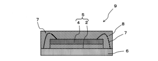
- FIG. 7 is a schematic longitudinal sectional view showing a preferred embodiment of a semiconductor package manufactured by the semiconductor package manufacturing method of the present invention.
- the thermally conductive film adhesive composition of the present invention (hereinafter also referred to as the adhesive composition of the present invention) is the thermally conductive film adhesive composition of the present invention (hereinafter referred to as the film adhesive of the present invention). ) is a composition suitable for forming.
- the adhesive composition of the present invention contains at least an epoxy resin (A), an epoxy resin curing agent (B), a polymer component (C), a polyhedral alumina filler (D), and a silane coupling agent (E). .
- polyhedral alumina accounts for the total content of epoxy resin (A), epoxy resin curing agent (B), polymer component (C), polyhedral alumina filler (D), and silane coupling agent (E).
- the proportion of filler (D) is controlled to 20 to 70% by volume.
- the content of the silane coupling agent (E) is controlled so that the silane coupling agent blending ratio shown in the following (Formula I) is 1.0 to 10.
- Silane coupling agent blending ratio Silane coupling agent (E) blending amount (g) / Silane coupling agent (E) required amount (g)
- Silane coupling agent (E) required amount (g) (polyhedral alumina filler (D) blending amount (g) x specific surface area of polyhedral alumina filler (D) (m 2 /g)) / silane coupling agent ( E) Minimum coverage area (m 2 /g)
- the specific surface area of the polyhedral alumina filler (D) was determined by the Brunauer-Emmett-Teller method (BET method) using nitrogen gas in accordance with the "carrier gas method" of JIS Z 8830:2013 (ISO 9277:2010).
- the adhesive composition of the present invention is in a pre-cured state.
- the blending ratio of the silane coupling agent and the blending amount of the silane coupling agent (E) shown in the above (Formula I) are both values in the adhesive composition of the present invention before curing.
- the meaning of "before curing” is the same as the meaning of "before curing” regarding the “thermally conductive film adhesive” described below.
- the mixing ratio of the silane coupling agent is preferably 1.1 to 9.0, more preferably 1.3 to 8.0, even more preferably 1.5 to 7.0, particularly preferably 1.5 to 4.0. , 1.6 to 2.5 are most preferred.
- the required amount of the above silane coupling agent (E) is preferably 0.20 to 3.50 g, more preferably 0.40 to 3.20 g, even more preferably 0.60 to 3.10 g, ⁇ 3.00g is more preferred, 0.80 ⁇ 2.00g is even more preferred, and 0.90 ⁇ 1.55g is particularly preferred.
- the required amount of the above silane coupling agent (E) can be 0.90 to 3.20 g, or 1.40 to 3.10 g.
- the epoxy resin (A) is a thermosetting resin having an epoxy group, and preferably has an epoxy equivalent of 500 g/eq or less.
- the epoxy resin (A) may be liquid, solid or semi-solid.
- liquid means that the softening point is less than 25°C
- solid means that the softening point is 60°C or higher
- semi-solid means that the softening point is equal to the softening point of the above liquid.
- the epoxy resin (A) used in the present invention should have a softening point of 100°C or lower from the viewpoint of obtaining a film adhesive that can reach a low melt viscosity in a suitable temperature range (for example, 60 to 120°C). It is preferable that there be.
- the softening point is a value measured by a softening point test (ring and ball method) (measurement conditions: based on JIS-K7234:1986).
- the epoxy equivalent is preferably 150 to 450 g/eq from the viewpoint of increasing the crosslinking density of the thermoset product.
- epoxy equivalent refers to the number of grams (g/eq) of a resin containing 1 gram equivalent of epoxy groups.
- the weight average molecular weight of the epoxy resin (A) is usually preferably less than 10,000, more preferably 5,000 or less. There is no particular limit to the lower limit, but 300 or more is practical.
- the weight average molecular weight is a value determined by GPC (Gel Permeation Chromatography) analysis (hereinafter, the same applies to other resins unless otherwise specified).
- the skeleton of the epoxy resin (A) includes phenol novolak type, orthocresol novolak type, cresol novolak type, dicyclopentadiene type, biphenyl type, fluorene bisphenol type, triazine type, naphthol type, naphthalene diol type, triphenylmethane type, Examples include tetraphenyl type, bisphenol A type, bisphenol F type, bisphenol AD type, bisphenol S type, and trimethylolmethane type. Among these, triphenylmethane type, bisphenol A type, cresol novolac type, and orthocresol novolak type are preferred from the viewpoint of obtaining a film adhesive having low resin crystallinity and good appearance.
- the content of the epoxy resin (A) is 100 parts by mass of the total content of components (specifically, components other than the solvent, i.e., solid content) constituting the film adhesive in the adhesive composition of the present invention.
- the amount is preferably 3 to 70 parts by weight, preferably 5 to 50 parts by weight, more preferably 8 to 30 parts by weight, and also preferably 8 to 20 parts by weight.
- Epoxy resin curing agent (B) As the epoxy resin curing agent (B), any curing agent such as amines, acid anhydrides, polyhydric phenols, etc. can be used.
- the present invention provides a film-like adhesive that has a low melt viscosity, exhibits curing properties at a high temperature exceeding a certain temperature, has fast curing properties, and has high storage stability that can be stored for a long time at room temperature. From this point of view, it is preferable to use a latent curing agent.
- latent curing agents examples include dicyandiamide compounds, imidazole compounds, curing catalyst complex polyhydric phenol compounds, hydrazide compounds, boron trifluoride-amine complexes, amine imide compounds, polyamine salts, and modified products and microcapsule types of these. can be mentioned. These may be used alone or in combination of two or more. It is more preferable to use an imidazole compound from the viewpoint of having better latent properties (excellent stability at room temperature and exhibiting curability by heating) and faster curing speed.
- the content of the epoxy resin curing agent (B) in the adhesive composition may be appropriately set depending on the type of curing agent and the reaction form.
- the amount may be 0.5 to 100 parts by weight, 1 to 80 parts by weight, 2 to 50 parts by weight, 4 to 20 parts by weight, based on 100 parts by weight of the epoxy resin (A). It is also preferable to do so.
- the amount of the imidazole compound is 0.5 to 10 parts by mass, and 2 to 9 parts by mass based on 100 parts by mass of the epoxy resin (A).
- the curing time can be further shortened.
- the content of the epoxy resin curing agent (B) By setting the content of the epoxy resin curing agent (B) to the above-mentioned preferable lower limit or more, the curing time can be further shortened.
- the content of the epoxy resin curing agent (B) By setting the content of the epoxy resin curing agent (B) to the above-mentioned preferable upper limit or less, film-like adhesion of excess curing agent can be achieved. Remaining in the agent can be suppressed. As a result, adsorption of moisture by the residual curing agent is suppressed, and the reliability of the semiconductor device can be improved.
- ⁇ Polymer component (C)> The above-mentioned polymer component (C) suppresses the film tackiness (the property that the film state tends to change even with a slight temperature change) at room temperature (25°C) when forming the film adhesive, and provides sufficient Any component may be used as long as it imparts adhesiveness and film-forming properties (film-forming properties).
- Natural rubber butyl rubber, isoprene rubber, chloroprene rubber, ethylene-vinyl acetate copolymer, ethylene-(meth)acrylic acid copolymer, ethylene-(meth)acrylic acid ester copolymer, polybutadiene resin, polycarbonate resin, thermoplastic Examples include polyimide resins, polyamide resins such as 6-nylon and 6,6-nylon, phenoxy resins, (meth)acrylic resins, polyester resins such as polyethylene terephthalate and polybutylene terephthalate, polyamideimide resins, fluororesins, polyurethane resins, etc. . These polymer components (C) may be used alone or in combination of two or more. As the polymer component (C), phenoxy resins, (meth)acrylic resins, and polyurethane resins are preferred.
- the mass average molecular weight of the polymer component (C) is 10,000 or more. There is no particular limit to the upper limit, but 5,000,000 or less is practical.
- the mass average molecular weight of the polymer component (C) is a value determined in terms of polystyrene by GPC [Gel Permeation Chromatography]. Hereinafter, the value of the mass average molecular weight of the specific polymer component (C) also has the same meaning.
- the glass transition temperature (Tg) of the polymer component (C) is preferably less than 100°C, more preferably less than 90°C.
- the lower limit is preferably 0°C or higher, more preferably 10°C or higher.
- the glass transition temperature of the polymer component (C) is the glass transition temperature measured by DSC at a heating rate of 0.1° C./min.
- the value of the glass transition temperature of the specific polymer component (C) also has the same meaning.
- the resin that can have an epoxy group such as phenoxy resin means that the epoxy resin (A) has an epoxy equivalent of 500 g/eq or less. , those that do not apply are classified as component (C).
- Phenoxy resin is preferable as the polymer component (C) because it has a similar structure to the epoxy resin (A) and has good compatibility. When a phenoxy resin is contained, an excellent adhesive effect can be exhibited.
- Phenoxy resin can be obtained by conventional methods. For example, phenoxy resins can be obtained by reacting bisphenols or biphenol compounds with epihalohydrins such as epichlorohydrin, or by reacting liquid epoxy resins with bisphenols or biphenol compounds.
- the weight average molecular weight of the phenoxy resin is preferably 10,000 or more, more preferably 10,000 to 100,000. Further, the amount of epoxy groups slightly remaining in the phenoxy resin is preferably 5000 g/eq or more in terms of epoxy equivalent.
- the glass transition temperature (Tg) of the phenoxy resin is preferably less than 100°C, more preferably less than 90°C.
- the lower limit is preferably 0°C or higher, more preferably 10°C or higher.
- the (meth)acrylic resin is not particularly limited, and resins made of known (meth)acrylic copolymers can be widely used as film components of film adhesives.
- the (meth)acrylic resin include poly(meth)acrylic acid esters or derivatives thereof.
- copolymers containing monomer components such as 2-hydroxyethyl acrylate, 2-hydroxyethyl methacrylate, 2-hydroxypropyl acrylate, 2-hydroxypropyl methacrylate, acrylic acid, methacrylic acid, itaconic acid, glycidyl methacrylate, glycidyl acrylate, etc. Can be mentioned.
- (meth)acrylic acid esters having a cyclic skeleton for example, (meth)acrylic acid cycloalkyl ester, (meth)acrylic acid benzyl ester, isobornyl (meth)acrylate, dicyclopentanyl (meth)acrylate, dicyclopentenyl Copolymers using (meth)acrylate, dicyclopentenyloxyethyl (meth)acrylate, imido(meth)acrylate, etc. as monomers are also preferred.
- (meth)acrylic acid alkyl esters in which the alkyl group has 1 to 18 carbon atoms for example, methyl (meth)acrylate, ethyl (meth)acrylate, propyl (meth)acrylate, and butyl (meth)acrylate. , etc. are also preferable as monomer components. It may also be copolymerized with vinyl acetate, (meth)acrylonitrile, styrene, or the like. It is preferable for the (meth)acrylic resin to have a hydroxyl group in terms of compatibility with the epoxy resin.
- the mass average molecular weight of the (meth)acrylic copolymer is preferably 10,000 to 2,000,000, more preferably 100,000 to 1,500,000.
- the glass transition temperature of the (meth)acrylic copolymer is preferably -35°C to 50°C, more preferably -10°C to 50°C, even more preferably 0°C to 40°C, particularly preferably 0°C to 30°C. in range.
- Polyurethane resin is a polymer having urethane (carbamate ester) bonds in its main chain.
- the polyurethane resin has a structural unit derived from a polyol, a structural unit derived from a polyisocyanate, and may further have a structural unit derived from a polycarboxylic acid.
- the polyurethane resins may be used alone or in combination of two or more.
- the Tg of the polyurethane resin is usually 100°C or less, preferably 60°C or less, more preferably 50°C or less, and also preferably 45°C or less.
- the weight average molecular weight of the polyurethane resin is not particularly limited, and those within the range of 5,000 to 500,000 are usually used.
- Polyurethane resins can be synthesized by conventional methods, or can also be obtained from the market. Commercially available products that can be used as polyurethane resins include Dynaleo VA-9320M, Dynaleo VA-9310MF, and Dynaleo VA-9303MF (all manufactured by Toyochem).
- the content of the polymer component (C) per 100 parts by mass of the epoxy resin (A) is preferably 1 to 40 parts by mass, more preferably 5 to 35 parts by mass, and even more preferably 10 to 30 parts by mass.
- the polyhedral alumina filler (D) is an inorganic powder containing alumina (aluminum oxide), and has a polyhedral shape.
- a "polyhedron" refers to a solid having multiple planes. The polyhedron only needs to have at least two planes, preferably four or more planes, and more preferably eight or more planes. Although the upper limit of the number of planes constituting the polyhedron is not particularly limited, for example, about 20 is practical.
- the shape of the plane is not particularly limited, and examples include polygons (triangle, quadrangle, pentagon, hexagon, etc.).
- a polyhedron may have a curved surface in addition to a flat surface.
- Examples of the polyhedron include a plate shape, a columnar shape, a square column, a cylinder, a regular polyhedron, and the like.
- the polyhedral alumina filler (D) contains true spherical alumina filler if the ratio of true spherical alumina filler to the total content of each of the above components (A) to (E) is about 1 to 50% by volume.
- the polyhedral alumina filler (D) may contain a polyhedral alumina filler and a spherical alumina filler, and in such a case, the polyhedral alumina filler and the spherical alumina filler may be combined. Together, they are referred to as polyhedral alumina filler (D).
- the true spherical alumina filler contained in the polyhedral alumina filler (D) can be 40% by volume or less, can be 30% by volume or less, can be 10% by volume or less, and 5. It can also be less than % by volume.
- the true spherical alumina filler contained in the polyhedral alumina filler (D) can be 80% by mass or less of the total amount of the polyhedral alumina filler (D), can be 50% by mass or less, can be 30% by mass, and can be 20% by mass. The amount can be 10% by mass or less.
- all the alumina fillers contained in the polyhedral alumina filler (D) can also be made into polyhedral alumina fillers.
- the preferred range of the average particle size of the polyhedral alumina filler (D) described below also applies to the average particle size of the true spherical alumina filler.
- the shape of the polyhedral alumina filler can be confirmed by observing it using a scanning electron microscope (SEM), and if two or more planes can be confirmed, it can be determined that it is a "polyhedral".
- SEM scanning electron microscope
- D polyhedral alumina filler
- the thermal conductivity is lower than when using true spherical alumina filler even with the same filling amount due to an increase in the contact area between fillers. It becomes possible to improve the performance.
- the average particle size (d50) of the polyhedral alumina filler (D) is not particularly limited, but from the viewpoint of making the film adhesive thinner, it is preferably 0.01 to 6.0 ⁇ m, and preferably 0.01 to 5.0 ⁇ m. , more preferably 0.1 to 4.0 ⁇ m, and even more preferably 0.3 to 3.5 ⁇ m.
- the average particle size (d50) is the so-called median diameter, which is the particle size when particle size distribution is measured by laser diffraction/scattering method and the cumulative distribution is 50% when the total volume of particles is 100%. means.
- the average particle size of the polyhedral alumina filler (D1) with a relatively large average particle size (d50) is The thickness is preferably 1.0 to 8.0 ⁇ m, more preferably 2.0 to 6.0 ⁇ m, even more preferably 2.5 to 5.0 ⁇ m, and even more preferably 2.5 to 4.0 ⁇ m.
- the average particle diameter (d50) of the polyhedral alumina filler (D2) having a relatively small average particle diameter (d50) is preferably 0.10 to 0.80 ⁇ m, more preferably 0.20 to 0.70 ⁇ m, and 0.
- the thickness is more preferably 30 to 0.70 ⁇ m, and even more preferably 0.35 to 0.65 ⁇ m.
- the value of the ratio of the content of the polyhedral alumina filler (D1) whose average particle size (d50) is relatively large to the content of the polyhedral alumina filler (D2) whose average particle size (d50) is relatively small (D1/D2) (mass ratio) is preferably 2 to 6, more preferably 3 to 5.
- a true spherical alumina filler with a relatively large average particle size (d50) can be used instead of a polyhedral alumina filler with a relatively large average particle size (d50).
- a true spherical alumina filler with a relatively small average particle size (d50) can be used instead of the relatively small polyhedral alumina filler.
- "perfectly spherical” does not correspond to the above-mentioned "polyhedron” and has a sphericity of 0.5 to 1.0 (preferably 0.6 to 1.0, more preferably 0.5 to 1.0). 7 to 1.0, more preferably 0.8 to 1.0).
- Sphericity can be determined by observing the alumina filler using a scanning electron microscope and based on its area and perimeter.
- the polyhedral alumina filler (D) may be surface-treated or surface-modified, and examples of surface treatment agents used for such surface treatment or surface modification include silane coupling agents, phosphoric acid or phosphoric acid compounds, Examples of surfactants other than those described in this specification include, for example, silane in the thermally conductive filler section of International Publication No. 2018/203527 or the aluminum nitride filler section of International Publication No. 2017/158994. The descriptions of coupling agents, phosphoric acid or phosphoric acid compounds and surfactants are applicable.
- silane coupling agent those used for surface treatment of inorganic fillers can be used without particular limitation.
- the above proportion to the total content of the epoxy resin (A), the epoxy resin curing agent (B), the polymer component (C), the polyhedral alumina filler (D), and the silane coupling agent (E) is The proportion of the polyhedral alumina filler (D) is 20 to 70% by volume.
- the content ratio of the polyhedral alumina filler (D) is equal to or higher than the lower limit, desired thermal conductivity and melt viscosity can be imparted to the film adhesive, and a heat dissipation effect from the semiconductor package can be obtained. .
- a desired melt viscosity can be imparted to the film adhesive, and the adhesive force with the adherend can be increased.
- the proportion of the polyhedral alumina filler (D) in the total content of components (A) to (E) is preferably 40 to 70% by volume, more preferably 45 to 70% by volume, and 50 to 70% by volume. is more preferable, 55 to 70% by volume is even more preferable, and even more preferably 55 to 65% by volume.
- the content (volume %) of the polyhedral alumina filler (D) can be calculated from the contained mass and specific gravity of each component (A) to (E).
- the adhesive composition of the present invention contains a silane coupling agent (E).
- the silane coupling agent used for the surface treatment of the polyhedral alumina filler (D) is silane It shall not be included in the coupling agent (E).
- a silane coupling agent is one in which at least one hydrolyzable group such as an alkoxy group or an aryloxy group is bonded to a silicon atom, and in addition, an alkyl group, an alkenyl group, or an aryl group is bonded to a silicon atom. Good too.
- the alkyl group preferably has an amino group, an alkoxy group, an epoxy group, or a (meth)acryloyloxy group as a substituent; ) Those having an acryloyloxy group as a substituent are more preferred, and those having an amino group as a substituent are particularly preferred.
- the silane coupling agent include 2-(3,4-epoxycyclohexyl)ethyltrimethoxysilane, 3-glycidyloxypropyltrimethoxysilane, 3-glycidyloxypropyltriethoxysilane, and 3-glycidyloxypropylmethyldimethoxysilane.
- Silane 3-glycidyloxypropylmethyldiethoxysilane, dimethyldimethoxysilane, dimethyldiethoxysilane, methyltrimethoxysilane, methyltriethoxysilane, phenyltrimethoxysilane, phenyltriethoxysilane, 3-aminopropyltrimethoxysilane, N -Phenyl-3-aminopropyltrimethoxysilane, 3-methacryloyloxipropylmethyldimethoxysilane, 3-methacryloyloxipropyltrimethoxysilane, 3-methacryloyloxipropylmethyldiethoxysilane, 3-methacryloyloxipropyltriethoxysilane, vinyl trimethoxysilane Examples include methoxysilane.
- the silane coupling agent (E) is blended to satisfy the silane coupling agent blending ratio expressed by the above-mentioned (Formula I).
- the adhesive composition of the present invention contains, in addition to an epoxy resin (A), an epoxy resin curing agent (B), a polymer component (C), a polyhedral alumina filler (D), and a silane coupling agent (E). , other additives such as organic solvents (methyl ethyl ketone, etc.), ion trapping agents, curing catalysts, viscosity modifiers, antioxidants, flame retardants, colorants, etc., to the extent that they do not impair the effects of the present invention. It may further contain. For example, "other additives" described in International Publication No. 2017/158994 can be included.
- the total content can be, for example, 60% by mass or more, preferably 70% by mass or more, more preferably 80% by mass or more, and can also be 90% by mass or more. Further, the above ratio may be 100% by mass, or may be 95% by mass or less.
- the adhesive composition of the present invention can be suitably used to obtain the film adhesive of the present invention. However, the present invention is not limited to film adhesives, and can also be suitably used to obtain liquid or paste adhesives, for example.
- the adhesive composition of the present invention can be obtained by mixing the above-mentioned components at a temperature at which the epoxy resin (A) practically does not harden.
- the order of mixing is not particularly limited. Resin components such as the epoxy resin (A) and the polymer component (C) are mixed together with a solvent if necessary, and then the polyhedral alumina filler (D), the epoxy resin curing agent (B), and the silane coupling agent (E ) may be mixed.
- mixing in the presence of the epoxy resin curing agent (B) may be carried out at a temperature at which the epoxy resin (A) does not actually harden, and the resin components in the absence of the epoxy resin curing agent (B) The mixing may be carried out at higher temperatures.
- the adhesive composition of the present invention is preferably stored at a temperature of 10° C. or lower before use (before forming into a film adhesive). .
- the thermally conductive film adhesive of the present invention is a film adhesive obtained from the adhesive composition of the present invention. Therefore, it contains the above-mentioned epoxy resin (A), epoxy resin curing agent (B), polymer component (C), polyhedral alumina filler (D), and silane coupling agent (E).
- epoxy resin A
- epoxy resin curing agent B
- polymer component C
- polyhedral alumina filler D
- silane coupling agent E
- additives other than organic solvents may be contained.
- the thermally conductive film adhesive of the present invention is specified as follows. Contains at least an epoxy resin (A), an epoxy resin curing agent (B), a polymer component (C), a polyhedral alumina filler (D), and a silane coupling agent (E), Accounting for the total content of the epoxy resin (A), the epoxy resin curing agent (B), the polymer component (C), the polyhedral alumina filler (D), and the silane coupling agent (E).
- the proportion of the polyhedral alumina filler (D) is 20 to 70% by volume
- Silane coupling agent blending ratio Silane coupling agent (E) blending amount (g) / Silane coupling agent (E) required amount (g)
- Silane coupling agent (E) required amount (g) [polyhedral alumina filler (D) blending amount (g) x specific surface area of polyhedral alumina filler (D) (m 2 /g)] / silane coupling agent ( E) Minimum coverage area (m 2 /g)
- the solvent is usually removed from the adhesive composition by drying. Therefore, the content of the solvent in the film adhesive of the present invention is 1000 ppm (ppm is based on mass) or less, and usually 0.1 to 1000 ppm.
- the term "film” means a thin film having a thickness of 200 ⁇ m or less. The shape, size, etc. are not particularly limited and can be adjusted as appropriate depending on the manner of use.
- the film adhesive of the present invention is in a state before curing, that is, in a B stage state.
- the film adhesive before curing refers to an adhesive in a state before the epoxy resin (A) is thermally cured.
- a film adhesive before thermosetting is one that has not been exposed to a temperature condition of 25°C or higher for 72 hours or more after preparation, and has not been exposed to a temperature condition of over 30°C. means a film adhesive that is not
- the film adhesive after curing refers to an epoxy resin (A) in a heat-cured state.
- the film adhesive of the present invention can be suitably used as a die attach film in semiconductor manufacturing processes.
- the film adhesive of the present invention has a melt viscosity of 250°C at 120°C when the film adhesive before thermosetting is heated from 25°C at a rate of 5°C/min. It is preferably in the range of ⁇ 10,000 Pa ⁇ s, more preferably in the range of 500 – 10,000 Pa ⁇ s, more preferably in the range of 600 – 9,200 Pa ⁇ s, and more preferably in the range of 700 – 8,000 Pa ⁇ s. is more preferable, and particularly preferably in the range of 2000 to 7200 Pa ⁇ s. Melt viscosity can be determined by the method described in Examples below.
- the melt viscosity is determined by the content of the polyhedral alumina filler (D), the particle size of the polyhedral alumina filler (D), the epoxy resin (A), the epoxy resin curing agent (B), and the polymer component (C). ) and silane coupling agent (E), etc., and the types and contents of the coexisting compounds or resins.
- the film adhesive of the present invention preferably has a thermal conductivity of 1.0 W/m ⁇ K or more, more preferably 1.0 to 5.0 W/m ⁇ K, and 1.5 to 4.5 W/m ⁇ K. m ⁇ K is more preferable, 1.7 to 4.5 W/m ⁇ K is even more preferable, and 2.3 to 4.2 W/m ⁇ K is particularly preferable.
- the thermal conductivity in the present invention is determined by the method described in Examples. That is, two silicon chips are bonded together via a film adhesive to form a silicon chip/film adhesive/silicon chip structure, and then the film adhesive is thermally cured to form a simulated semiconductor package. .
- the thermal resistance of the film adhesive in the form of a simulated semiconductor package is measured using DynTIM Tester (+T3Ster) manufactured by Mentor Graphics.
- DynTIM Tester (+T3Ster) manufactured by Mentor Graphics.
- the measurement conditions for thermal resistance the measurement conditions described in Examples can be used.
- the thermal conductivity can generally be calculated by the following formula (3) from the thickness of the sample and the value of thermal resistance.
- ⁇ (W/m ⁇ K, thermal conductivity) L (m, sample thickness)/R (m 2 ⁇ K/W, sample thermal resistance)
- the thickness of the film adhesive is set to 10 ⁇ m, 20 ⁇ m, and 50 ⁇ m, and the thermal resistance at each thickness is measured, and the obtained thermal resistance at each thickness is plotted against the thickness, and approximated by the least squares method. A straight line is obtained, and the thermal conductivity (package form thermal conductivity) is calculated as the reciprocal of its slope. By doing this, it is possible to cancel the thermal resistance caused by the equipment used for measurement (including silicon chips placed above and below the film adhesive), and it is possible to accurately measure the thermal conductivity of the film adhesive itself. I can do it. According to the above measurement method, the thermal conductivity of the film adhesive itself can be evaluated in a state closer to the actual usage environment (mounted state).
- the film adhesive of the present invention preferably has a die shear strength of 20 MPa or more at 25°C. It is preferable that the die shear strength is within the above range because the semiconductor chip can be reliably bonded to the adherend. Die shear strength can be measured by the method described in Examples.
- the film adhesive of the present invention preferably has a thickness of 1 to 80 ⁇ m, more preferably 1 to 50 ⁇ m, and even more preferably 1 to 20 ⁇ m.
- the thickness of the film adhesive can be measured by a contact/linear gauge method (desktop contact type thickness measuring device).
- the film adhesive of the present invention is formed by preparing the adhesive composition (varnish) of the present invention, applying this composition onto a release-treated base film, and drying as necessary. can do.
- Adhesive compositions usually contain an organic solvent.
- the release-treated base film may be any film that functions as a cover film for the obtained film adhesive, and any known film may be used as appropriate. Examples include release-treated polypropylene (PP), release-treated polyethylene (PE), and release-treated polyethylene terephthalate (PET).
- PP release-treated polypropylene
- PE release-treated polyethylene
- PET release-treated polyethylene terephthalate
- any known method can be appropriately employed, and examples thereof include methods using a roll knife coater, a gravure coater, a die coater, a reverse coater, and the like. Drying may be performed as long as the organic solvent is removed from the adhesive composition to form a film adhesive without curing the epoxy resin (A), for example, by holding at a temperature of 80 to 150°C
- the film adhesive of the present invention may be composed of the film adhesive of the present invention alone, or may be formed by laminating the above-mentioned release-treated base film on at least one surface of the film adhesive. It may be a form. Furthermore, it may be integrated with a dicing film to form a dicing/die attach film. Further, the film adhesive of the present invention may be in the form of a film cut out to an appropriate size, or may be in the form of a film wound into a roll.
- the film adhesive of the present invention is preferably stored at a temperature of 10° C. or lower before use (before curing) from the viewpoint of suppressing curing of the epoxy resin (A).
- FIG. 1 to 7 are schematic longitudinal cross-sectional views showing a preferred embodiment of each step of the method for manufacturing a semiconductor package of the present invention.
- the film adhesive 2 (die attach film 2) of the present invention is thermocompression bonded to the surface (on which no circuit is formed) to form an adhesive layer (film adhesive 2).
- a dicing film 3 (dicing tape 3) is provided via the adhesive 2).
- the film adhesive 2 is shown smaller than the dicing film 3, but the sizes (areas) of both films are appropriately set depending on the purpose.
- the thermocompression bonding is carried out at a temperature at which the epoxy resin (A) is not practically cured by heat. For example, conditions include a temperature of about 70° C. and a pressure of about 0.3 MPa.
- a semiconductor wafer having at least one semiconductor circuit formed on its surface can be appropriately used, and examples thereof include a silicon wafer, a SiC wafer, a GaAs wafer, and a GaN wafer.
- a known device such as a roll laminator or a manual laminator can be used as appropriate.
- the die attach film and the dicing film are attached separately, but when the film adhesive of the present invention is in the form of a dicing/die attach film, the film adhesive and the dicing film are attached together. Can be pasted together.
- the semiconductor wafer 1 and the adhesive layer are diced together, and the semiconductor wafer is diced onto the dicing film 3.
- a semiconductor chip 5 with an adhesive layer is obtained, which includes a semiconductor chip 4 with a film-like adhesive layer and film-like adhesive pieces 2 in which the film-like adhesive 2 is cut into pieces.
- the dicing device is not particularly limited, and a normal dicing device can be used as appropriate.
- the semiconductor chip 5 with the adhesive layer is peeled off from the dicing film 3.
- the dicing film may be cured with energy rays to reduce the adhesive strength. Peeling can be performed by picking up the semiconductor chip 5 with the adhesive layer.
- the semiconductor chip 5 with the adhesive layer and the wiring board 6 are bonded together by thermocompression via the film adhesive piece 2, and the semiconductor chip 5 with the adhesive layer is mounted on the wiring board 6.
- the wiring board 6 a board on which a semiconductor circuit is formed can be used as appropriate, such as a printed circuit board (PCB), various lead frames, and electronic components such as resistive elements and capacitors mounted on the board surface. Examples include substrates that have been
- the method of mounting the semiconductor chip 5 with an adhesive layer on such a wiring board 6 is not particularly limited, and a conventional mounting method using thermocompression bonding can be adopted as appropriate.
- thermosetting temperature is not particularly limited as long as it is at least the thermosetting start temperature of the film adhesive piece 2, and the types of epoxy resin (A), polymer component (C), and epoxy curing agent (B) used can be determined. will be adjusted accordingly.
- the temperature is preferably 100 to 180°C, and more preferably 140 to 180°C from the viewpoint of curing in a shorter time. If the temperature is too high, the components in the film adhesive piece 2 will tend to volatilize and foam during the curing process.
- the time for this thermosetting treatment may be appropriately set depending on the heating temperature, and can be, for example, 10 to 120 minutes.
- connection method is not particularly limited, and conventionally known methods such as a wire bonding method, a TAB (Tape Automated Bonding) method, etc. can be appropriately employed.
- a plurality of semiconductor chips 4 can be stacked by thermocompression bonding and thermosetting another semiconductor chip 4 on the surface of the mounted semiconductor chip 4, and then connecting it to the wiring board 6 again using a wire bonding method.
- the semiconductor chips are stacked while being shifted, or as shown in FIG. 6, the thickness of the film-like adhesive piece 2 from the second layer onward is increased so that the bonding wire 7 is embedded in the stack. etc.
- the sealing resin 8 is not particularly limited, and any known sealing resin that can be used for manufacturing semiconductor packages can be used. Furthermore, the method of sealing with the sealing resin 8 is not particularly limited, and any commonly used method may be employed.
- the semiconductor package of the present invention is manufactured by the above-described semiconductor package manufacturing method, and the semiconductor chip and the wiring board, or at least one location between the semiconductor chips, are bonded with the thermoset of the film-like adhesive of the present invention. There is.
- Triphenylmethane type epoxy resin (trade name: EPPN-501H, weight average molecular weight: 1000, softening point: 55°C, solid, epoxy equivalent: 167 g/eq, manufactured by Nippon Kayaku Co., Ltd.) 56 parts by mass, bisphenol A type 49 parts by mass of epoxy resin (trade name: YD-128, weight average molecular weight: 400, softening point: 25°C or lower, liquid, epoxy equivalent: 190 g/eq, manufactured by Shinnikka Epoxy Manufacturing Co., Ltd.), and bisphenol A 30 parts by mass of type phenoxy resin (trade name: YP-50, weight average molecular weight: 70000, Tg: 84°C, manufactured by Shin Nikka Epoxy Manufacturing Co., Ltd.) and 67 parts by mass of MEK were placed in a 1000 ml separable flask at a temperature of The mixture was heated and stirred at 110° C.
- EPPN-501H weight average molecular weight: 1000, softening point:
- a mixed varnish (adhesive composition) was obtained.
- the obtained mixed varnish was applied onto a release-treated PET film with a thickness of 38 ⁇ m and dried by heating (held at 130° C. for 10 minutes), so that the thickness of the film adhesive was 10 ⁇ m, 20 ⁇ m, or 50 ⁇ m.
- a film adhesive with a release film was obtained.
- Example 2 An adhesive composition and a film adhesive with a release film were obtained in the same manner as in Example 1, except that the amount of polyhedral alumina filler was 319 parts by mass.
- Example 3 An adhesive composition and a film adhesive with a release film were obtained in the same manner as in Example 1, except that the amount of polyhedral alumina filler was 478 parts by mass.
- Example 4 As a filler, 383 parts by mass of polyhedral alumina filler (trade name: AA-3, average particle size (d50): 3.5 ⁇ m, specific surface area: 0.6 m 2 /g, manufactured by Sumitomo Chemical Co., Ltd.) and polyhedral alumina Example 1 except that 96 parts by mass of filler (trade name: AA-05, average particle size (d50): 0.58 ⁇ m, specific surface area: 3.2 m 2 /g, manufactured by Sumitomo Chemical Co., Ltd.) was used. An adhesive composition and a film adhesive with a release film were obtained in the same manner as above.
- Example 5 The blending amount of the silane coupling agent was 4.5 parts by mass, and the filler was polyhedral alumina filler (trade name: AA-3, average particle size (d50): 3.5 ⁇ m, specific surface area: 0.6 m 2 /g). , manufactured by Sumitomo Chemical Co., Ltd.) 580 parts by mass and polyhedral alumina filler (trade name: AA-05, average particle size (d50): 0.58 ⁇ m, specific surface area: 3.2 m 2 /g, Sumitomo Chemical Co., Ltd.) An adhesive composition and a film-like adhesive with a release film were obtained in the same manner as in Example 1, except that 145 parts by mass of the adhesive was used.
- Example 6 The blending amount of the silane coupling agent was 5.5 parts by mass, and the filler was polyhedral alumina filler (trade name: AA-3, average particle size (d50): 3.5 ⁇ m, specific surface area: 0.6 m 2 /g). , manufactured by Sumitomo Chemical Co., Ltd.) and polyhedral alumina filler (trade name: AA-05, average particle size (d50): 0.58 ⁇ m, specific surface area: 3.2 m 2 /g, Sumitomo Chemical Co., Ltd.) An adhesive composition and a film-like adhesive with a release film were obtained in the same manner as in Example 1, except that 181 parts by mass of the adhesive composition was used.
- Example 7 As a silane coupling agent, 3.0 parts by mass of a silane coupling agent (vinyltrimethoxysilane, trade name: KBM-1003, minimum coverage area of silane coupling agent: 515 m 2 /g, manufactured by Shin-Etsu Chemical Co., Ltd.) was added. An adhesive composition and a film-like adhesive with a release film were obtained in the same manner as in Example 4, except that they were used.
- a silane coupling agent vinyltrimethoxysilane, trade name: KBM-1003, minimum coverage area of silane coupling agent: 515 m 2 /g, manufactured by Shin-Etsu Chemical Co., Ltd.
- Example 8 As a silane coupling agent, a silane coupling agent (3-aminopropyltrimethoxysilane, trade name: KBM-903, minimum coverage area of silane coupling agent: 353 m 2 /g, manufactured by Shin-Etsu Chemical Co., Ltd.) 3.0 An adhesive composition and a film adhesive with a release film were obtained in the same manner as in Example 4, except that parts by mass were used.
- a silane coupling agent 3-aminopropyltrimethoxysilane, trade name: KBM-903, minimum coverage area of silane coupling agent: 353 m 2 /g, manufactured by Shin-Etsu Chemical Co., Ltd.
- Example 9 As a silane coupling agent, a silane coupling agent (3-glycidyloxypropylmethyldimethoxysilane, trade name: KBM-402, silane coupling agent minimum coverage area: 354 m 2 /g, manufactured by Shin-Etsu Chemical Co., Ltd.)3.
- An adhesive composition and a film adhesive with a release film were obtained in the same manner as in Example 4, except that 0 part by mass was used.
- Example 10 instead of the phenoxy resin, a urethane resin solution (trade name: Dynaleo VA-9310MF, weight average molecular weight: 110000, Tg: 27°C, storage modulus: 289 MPa, solvent: MEK/IPA mixed solvent, manufactured by Toyochem Co., Ltd.) 120
- An adhesive composition and a film adhesive with a release film were obtained in the same manner as in Example 4, except that parts by mass (including 30 parts by mass of urethane resin) were blended.
- Example 11 Instead of phenoxy resin, 30 parts by mass of acrylic resin (trade name: SG-280EK23, weight average molecular weight: 800000, Tg: -29°C, storage modulus: 6.5 MPa, manufactured by Nagase ChemteX Co., Ltd.) was blended. An adhesive composition and a film adhesive with a release film were obtained in the same manner as in Example 4, except that 90 parts by mass of cyclohexanone were blended.
- acrylic resin trade name: SG-280EK23, weight average molecular weight: 800000, Tg: -29°C, storage modulus: 6.5 MPa, manufactured by Nagase ChemteX Co., Ltd.
- Example 12 As fillers, 383 parts by mass of polyhedral alumina filler (trade name: AA-3, average particle size (d50): 3.5 ⁇ m, specific surface area: 0.6 m 2 /g, manufactured by Sumitomo Chemical Co., Ltd.) and true spherical alumina were used. 96 parts by mass of filler (trade name: AO502, average particle size (d50): 0.2 ⁇ m, specific surface area: 8.0 m 2 /g, sphericity 0.99, manufactured by Admatex) was blended, and silane coupling was performed.
- AO502 average particle size (d50): 0.2 ⁇ m, specific surface area: 8.0 m 2 /g, sphericity 0.99, manufactured by Admatex
- Example 12 An adhesive composition and a film-like adhesive with a release film were obtained in the same manner as in Example 4, except that the blending amount of the agent was 5.0 parts by mass.
- the proportion (volume %) of the true spherical alumina filler in the total content of the epoxy resin, epoxy resin curing agent, polymer component, silane coupling agent, and inorganic filler was 10 volume %. there were.
- spherical alumina filler product name: AZ2-75, average particle size (d50): 3.0 ⁇ m, specific surface area: 1.3 m 2 /g, sphericity: 0.99, Nippon Steel Chemical & Materials Co., Ltd.
- Example 13 (manufactured by Sumitomo Chemical Co., Ltd.) 383 parts by mass and 96 parts by mass of polyhedral alumina filler (trade name: AA-05, average particle size (d50): 0.58 ⁇ m, specific surface area: 3.2 m 2 /g, manufactured by Sumitomo Chemical Co., Ltd.)
- An adhesive composition and a film adhesive with a release film were obtained in the same manner as in Example 4, except that the amount of the silane coupling agent was 5.0 parts by mass.
- the proportion (volume %) of the true spherical alumina filler in the total content of the epoxy resin, epoxy resin curing agent, polymer component, silane coupling agent, and inorganic filler was 40 volume %. there were.
- Example 4 As a filler, 428 parts by mass of polyhedral alumina filler (trade name: AA-3, average particle size (d50): 3.5 ⁇ m, specific surface area: 0.6 m 2 /g, manufactured by Sumitomo Chemical Co., Ltd.) and polyhedral alumina 107 parts by mass of filler (trade name: AA-05, average particle size (d50): 0.58 ⁇ m, specific surface area: 3.2 m 2 /g, manufactured by Sumitomo Chemical Co., Ltd.) was blended, and a silane coupling agent was blended.
- An adhesive composition and a film adhesive with a release film were obtained in the same manner as in Example 8, except that the amount was 20.0 parts by mass.
- polyhedral alumina filler (trade name: AA-3, average particle size (d50): 3.5 ⁇ m, specific surface area: 0.6 m 2 /g, manufactured by Sumitomo Chemical Co., Ltd.) 377 mass and polyhedral alumina filler (Product name: AA-05, average particle size (d50): 0.58 ⁇ m, specific surface area: 3.2 m 2 /g, manufactured by Sumitomo Chemical Co., Ltd.) 94 parts by mass, and the amount of silane coupling agent blended
- An adhesive composition and a film-like adhesive with a release film were obtained in the same manner as in Example 4, except that the amount of adhesive was 0.8 parts by mass.
- spherical alumina filler (product name: AZ2-75, average particle size (d50): 3.0 ⁇ m, specific surface area: 1.3 m 2 /g, sphericity: 0.99, Nippon Steel Chemical & Materials Co., Ltd. (product name: ASFP-05S, average particle size (d50): 0.6 ⁇ m, specific surface area: 3.6 m 2 /g, sphericity: 0.99, manufactured by Denka Corporation)
- An adhesive composition and a film adhesive with a release film were obtained in the same manner as in Example 4, except that 95 parts by mass of the silane coupling agent was used and the amount of the silane coupling agent was 1.3 parts by mass.
- spherical alumina filler product name: AZ2-75, average particle size (d50): 3.0 ⁇ m, specific surface area: 1.3 m 2 /g, sphericity: 0.99, Nippon Steel Chemical & Materials Co., Ltd.
- spherical alumina filler (product name: AZ2-75, average particle size (d50): 3.0 ⁇ m, specific surface area: 1.3 m 2 /g, sphericity: 0.99, Nippon Steel Chemical & Materials Co., Ltd. (product name: ASFP-05S, average particle size (d50): 0.6 ⁇ m, specific surface area: 3.6 m 2 /g, sphericity: 0.99, manufactured by Denka Corporation)
- An adhesive composition and a film adhesive with a release film were obtained in the same manner as in Example 6, except that 177 parts by mass of the silane coupling agent was used and the amount of the silane coupling agent was 2.4 parts by mass.
- spherical alumina filler product name: AZ2-75, average particle size (d50): 3.0 ⁇ m, specific surface area: 1.3 m 2 /g, sphericity: 0.99, Nippon Steel Chemical & Materials Co., Ltd.
- An adhesive composition and a film-like adhesive with a release film were obtained in the same manner as in Reference Example 4, except that 202 parts by mass of the silane coupling agent was used and the amount of silane coupling agent was 0.4 parts by mass. .
- Tables 1 to 3 show the compositions of the film adhesives prepared in each Example, Comparative Example, and Reference Example. A blank column means that the component is not contained.
- "Inorganic filler content” shown in Tables 1 to 3 refers to the inorganic filler content in the total content of epoxy resin, epoxy resin curing agent, polymer component, silane coupling agent, and inorganic filler. The percentage (volume %) is shown.
- This test is a test to evaluate the thermal conductivity of a single film adhesive. Cut the film adhesive with a thickness of 10 ⁇ m obtained in each example, comparative example, and reference example into a square piece with a side of 50 mm or more, and cut the cut square piece (film adhesive) so that the thickness is 5 mm or more. were laminated to obtain a laminate. The obtained laminate was placed on a disc-shaped mold with a diameter of 50 mm and a thickness of 5 mm, heated using a compression press molding machine at a temperature of 150°C and a pressure of 2 MPa for 10 minutes, taken out, and then placed in a dryer. The film adhesive was thermally cured by heating at 180° C.
- the film adhesive with a 10 ⁇ m release film obtained in each Example, Comparative Example, and Reference Example was coated at a temperature of 70°C using a manual laminator (trade name: FM-114, manufactured by Technovision). It was bonded to one side of a dummy silicon wafer (8 inch size, 365 ⁇ m thick) under a pressure of 0.3 MPa. Thereafter, after peeling off the release film from the film adhesive, using the same manual laminator, place a dicing tape on the surface of the film adhesive opposite to the dummy silicon wafer at room temperature and under a pressure of 0.3 MPa.
- a manual laminator trade name: FM-114, manufactured by Technovision
- a dicing device product name: DFD-6340, product name: DFD-6340, Dicing was performed from the dummy silicon wafer side using a dummy silicon wafer (manufactured by DISCO) to form squares of 2 mm x 2 mm in size, and the individual pieces with a film adhesive (adhesive layer) were placed on the dicing film.
- a dummy chip semiconductor chip
- dicing tape product name: K-8
- a dicing frame (trade name: DTF2-8-1H001, manufactured by DISCO) were adhered.
- a dicing device product name: DFD-6340, product name: DFD-6340, Dicing was carried out from the silicon wafer side using a silicon wafer (manufactured by DISCO) into squares of 12 mm x 12 mm to obtain individualized silicon chips on a dicing film.
- the dummy chip with film adhesive was picked up from the dicing tape using a die bonder (product name: DB-800, manufactured by Hitachi High-Technologies Corporation), and was heated at 120° C. and under a pressure of 0.5 MPa (load: 200 gf) for a period of time. Under the condition of 1.0 seconds, the film-like adhesive side of the film-like adhesive-attached dummy chip and the mounting surface side (uneven surface) of the 12 mm x 12 mm silicon chip were bonded together by thermocompression bonding. did. At this time, two 2 mm x 2 mm dummy chips coated with a film-like adhesive were spaced apart from each other on the mounting surface side of the 12 mm x 12 mm silicon chip.
- the die shear strength of eight dummy chips with film-like adhesive was measured, and the average value thereof was calculated (average die shear strength) and evaluated based on the following criteria.
- --Evaluation criteria-- AA The average die shear strength is 20 MPa or more, and the die shear strength of all eight film-like adhesive-attached dummy chips is 20 MPa or more.
- A The average die shear strength is 20 MPa or more, but there are 5 to 7 dummy chips with a film adhesive having a die shear strength of 20 MPa or more.
- B Average die shear strength is less than 20 MPa.
- a dicing tape A product name: K-13 (manufactured by Furukawa Electric Co., Ltd.) and a dicing frame (product name: DTF2-8-1H001, manufactured by DISCO) were adhered.
- a dicing device product name: DFD-6340, product name: DFD-6340, Dicing was performed from the dummy silicon wafer side using a dummy silicon wafer (manufactured by DISCO) into a square of 10 mm x 10 mm to obtain individual film-like adhesive-attached dummy chips on the dicing film.
- dicing tape product name: K-8
- a dicing frame (trade name: DTF2-8-1H001, manufactured by DISCO) were adhered.
- a dicing device product name: DFD-6340, product name: DFD-6340, Dicing was carried out from the silicon wafer side using a silicon wafer (manufactured by DISCO) into squares of 12 mm x 12 mm to obtain individualized silicon chips on a dicing film.
- the film-like adhesive-attached dummy chip was picked up from the dicing tape using a die bonder (product name: DB-800, manufactured by Hitachi High-Technologies Corporation), and was heated at 120° C. and under a pressure of 1.0 MPa (load: 1000 gf) for a period of time. Under the condition of 1.5 seconds, the film-like adhesive side of the film-like adhesive-attached dummy chip and the mounting surface side of the 12 mm x 12 mm size silicon chip were bonded together by thermocompression. At this time, a 10 mm x 10 mm film-like adhesive-attached dummy chip was placed in the center of the implementation surface of the 12 mm x 12 mm silicon chip.
- a die bonder product name: DB-800, manufactured by Hitachi High-Technologies Corporation
- the thermal resistance of the film adhesive in each of these simulated semiconductor packages was measured using a DynTIM Tester (+T3Ster) manufactured by Mentor Graphics under the following conditions. Atmosphere: In the air Measurement direction: Thickness direction Measurement temperature: 23°C (low temperature side base temperature) Temperature rise: 5 to 15°C (temperature difference between the top and bottom surfaces of the sample) In this test, the obtained thermal resistance value was plotted against the thickness, and the package form thermal conductivity was calculated as the reciprocal of the slope. By doing so, the thermal resistance due to the equipment used for the measurement (including semiconductor chips and silicon chips placed above and below the film adhesive) was canceled, and the thermal conductivity of the film adhesive itself was measured. The package form thermal conductivity thus obtained was evaluated based on the following evaluation criteria.
- the thermal conductivity of the package form is 2.5 W/m ⁇ K or more.
- AA The thermal conductivity of the package form is 1.5 W/m ⁇ K or more and less than 2.5 W/m ⁇ K.
- a film-like adhesive with high adhesion to adherends and excellent thermal conductivity can be formed even if it contains polyhedral alumina filler as an inorganic filler. I know what I can do. Furthermore, it can be seen that the film adhesives of Examples 1 to 13 are less likely to form voids at the interface with the adherend and have excellent package assemblability.
Landscapes
- Chemical & Material Sciences (AREA)
- Organic Chemistry (AREA)
- Health & Medical Sciences (AREA)
- Chemical Kinetics & Catalysis (AREA)
- Medicinal Chemistry (AREA)
- Polymers & Plastics (AREA)
- Inorganic Chemistry (AREA)
- Adhesives Or Adhesive Processes (AREA)
- Die Bonding (AREA)
- Dicing (AREA)
- Adhesive Tapes (AREA)
Priority Applications (4)
| Application Number | Priority Date | Filing Date | Title |
|---|---|---|---|
| JP2023547073A JP7383206B1 (ja) | 2022-03-30 | 2023-03-27 | 熱伝導性フィルム状接着剤用組成物及び熱伝導性フィルム状接着剤、並びに、熱伝導性フィルム状接着剤を用いた半導体パッケージ及びその製造方法 |
| KR1020237033113A KR102742635B1 (ko) | 2022-03-30 | 2023-03-27 | 열 전도성 필름형 접착제용 조성물 및 열 전도성 필름형 접착제, 그리고 열 전도성 필름형 접착제를 사용한 반도체 패키지 및 그 제조 방법 |
| CN202380017916.5A CN118696105A (zh) | 2022-03-30 | 2023-03-27 | 导热性膜状粘接剂用组合物和导热性膜状粘接剂、以及使用导热性膜状粘接剂的半导体封装及其制造方法 |
| US18/756,411 US20240352289A1 (en) | 2022-03-30 | 2024-06-27 | Thermally conductive film adhesive composition and thermally conductive film adhesive, and semiconductor package using thermally conductive film adhesive and producing method thereof |
Applications Claiming Priority (2)
| Application Number | Priority Date | Filing Date | Title |
|---|---|---|---|
| JP2022-055427 | 2022-03-30 | ||
| JP2022055427 | 2022-03-30 |
Related Child Applications (1)
| Application Number | Title | Priority Date | Filing Date |
|---|---|---|---|
| US18/756,411 Continuation US20240352289A1 (en) | 2022-03-30 | 2024-06-27 | Thermally conductive film adhesive composition and thermally conductive film adhesive, and semiconductor package using thermally conductive film adhesive and producing method thereof |
Publications (1)
| Publication Number | Publication Date |
|---|---|
| WO2023190321A1 true WO2023190321A1 (ja) | 2023-10-05 |
Family
ID=88202285
Family Applications (1)
| Application Number | Title | Priority Date | Filing Date |
|---|---|---|---|
| PCT/JP2023/012170 Ceased WO2023190321A1 (ja) | 2022-03-30 | 2023-03-27 | 熱伝導性フィルム状接着剤用組成物及び熱伝導性フィルム状接着剤、並びに、熱伝導性フィルム状接着剤を用いた半導体パッケージ及びその製造方法 |
Country Status (6)
| Country | Link |
|---|---|
| US (1) | US20240352289A1 (https=) |
| JP (1) | JP7383206B1 (https=) |
| KR (1) | KR102742635B1 (https=) |
| CN (1) | CN118696105A (https=) |
| TW (1) | TWI844320B (https=) |
| WO (1) | WO2023190321A1 (https=) |
Cited By (1)
| Publication number | Priority date | Publication date | Assignee | Title |
|---|---|---|---|---|
| WO2024162415A1 (ja) * | 2023-01-31 | 2024-08-08 | 積水化学工業株式会社 | 硬化性熱伝導性接着剤、及びその供給形態 |
Families Citing this family (1)
| Publication number | Priority date | Publication date | Assignee | Title |
|---|---|---|---|---|
| WO2025183038A1 (ja) * | 2024-02-27 | 2025-09-04 | 日東シンコー株式会社 | 接着シート |
Citations (7)
| Publication number | Priority date | Publication date | Assignee | Title |
|---|---|---|---|---|
| WO2013187303A1 (ja) * | 2012-06-12 | 2013-12-19 | 三菱瓦斯化学株式会社 | 樹脂組成物、プリプレグ、金属箔張積層板及びプリント配線板 |
| WO2017191801A1 (ja) * | 2016-05-06 | 2017-11-09 | Dic株式会社 | 樹脂組成物、成形体、積層体及び接着剤 |
| JP2018134779A (ja) * | 2017-02-21 | 2018-08-30 | 日立化成株式会社 | 多層樹脂シート、多層樹脂シートの製造方法、多層樹脂シート硬化物、多層樹脂シート積層体、及び多層樹脂シート積層体硬化物 |
| JP2019021829A (ja) * | 2017-07-20 | 2019-02-07 | 日立化成株式会社 | 放熱性ダイボンディングフィルム及びダイシングダイボンディングフィルム |
| JP2021050305A (ja) * | 2019-09-26 | 2021-04-01 | 昭和電工マテリアルズ株式会社 | 樹脂シート及びパワー半導体装置 |
| JP2022027972A (ja) * | 2016-02-26 | 2022-02-14 | 昭和電工マテリアルズ株式会社 | 接着フィルム |
| JP7042986B1 (ja) * | 2020-07-30 | 2022-03-28 | 古河電気工業株式会社 | 接着剤用組成物及びフィルム状接着剤、並びに、フィルム状接着剤を用いた半導体パッケージ及びその製造方法 |
Family Cites Families (7)
| Publication number | Priority date | Publication date | Assignee | Title |
|---|---|---|---|---|
| JP2005171206A (ja) * | 2003-12-15 | 2005-06-30 | Toyota Motor Corp | 樹脂配合用粉体混合物及び樹脂組成物 |
| CN104334604A (zh) * | 2012-05-17 | 2015-02-04 | 太阳油墨制造株式会社 | 碱显影型的热固化性树脂组合物、印刷电路板 |
| JP6366228B2 (ja) | 2013-06-04 | 2018-08-01 | 日東電工株式会社 | 接着シート、及びダイシング・ダイボンディングフィルム |
| CN105659711A (zh) * | 2013-10-17 | 2016-06-08 | 住友电木株式会社 | 环氧树脂组合物、带有树脂层的载体材料、金属基电路基板和电子装置 |
| JP2016104832A (ja) | 2014-12-01 | 2016-06-09 | Dic株式会社 | 樹脂組成物、熱伝導性接着剤、熱伝導性接着シート及び積層体 |
| WO2021033368A1 (ja) | 2019-08-22 | 2021-02-25 | 古河電気工業株式会社 | 接着剤用組成物、フィルム状接着剤及びその製造方法、並びに、フィルム状接着剤を用いた半導体パッケージおよびその製造方法 |
| CN117255839A (zh) * | 2021-07-13 | 2023-12-19 | 古河电气工业株式会社 | 导热性膜状粘接剂、半导体封装及其制造方法 |
-
2023
- 2023-03-27 JP JP2023547073A patent/JP7383206B1/ja active Active
- 2023-03-27 KR KR1020237033113A patent/KR102742635B1/ko active Active
- 2023-03-27 CN CN202380017916.5A patent/CN118696105A/zh active Pending
- 2023-03-27 WO PCT/JP2023/012170 patent/WO2023190321A1/ja not_active Ceased
- 2023-03-28 TW TW112111748A patent/TWI844320B/zh active
-
2024
- 2024-06-27 US US18/756,411 patent/US20240352289A1/en active Pending
Patent Citations (7)
| Publication number | Priority date | Publication date | Assignee | Title |
|---|---|---|---|---|
| WO2013187303A1 (ja) * | 2012-06-12 | 2013-12-19 | 三菱瓦斯化学株式会社 | 樹脂組成物、プリプレグ、金属箔張積層板及びプリント配線板 |
| JP2022027972A (ja) * | 2016-02-26 | 2022-02-14 | 昭和電工マテリアルズ株式会社 | 接着フィルム |
| WO2017191801A1 (ja) * | 2016-05-06 | 2017-11-09 | Dic株式会社 | 樹脂組成物、成形体、積層体及び接着剤 |
| JP2018134779A (ja) * | 2017-02-21 | 2018-08-30 | 日立化成株式会社 | 多層樹脂シート、多層樹脂シートの製造方法、多層樹脂シート硬化物、多層樹脂シート積層体、及び多層樹脂シート積層体硬化物 |
| JP2019021829A (ja) * | 2017-07-20 | 2019-02-07 | 日立化成株式会社 | 放熱性ダイボンディングフィルム及びダイシングダイボンディングフィルム |
| JP2021050305A (ja) * | 2019-09-26 | 2021-04-01 | 昭和電工マテリアルズ株式会社 | 樹脂シート及びパワー半導体装置 |
| JP7042986B1 (ja) * | 2020-07-30 | 2022-03-28 | 古河電気工業株式会社 | 接着剤用組成物及びフィルム状接着剤、並びに、フィルム状接着剤を用いた半導体パッケージ及びその製造方法 |
Cited By (1)
| Publication number | Priority date | Publication date | Assignee | Title |
|---|---|---|---|---|
| WO2024162415A1 (ja) * | 2023-01-31 | 2024-08-08 | 積水化学工業株式会社 | 硬化性熱伝導性接着剤、及びその供給形態 |
Also Published As
| Publication number | Publication date |
|---|---|
| CN118696105A (zh) | 2024-09-24 |
| US20240352289A1 (en) | 2024-10-24 |
| TWI844320B (zh) | 2024-06-01 |
| JPWO2023190321A1 (https=) | 2023-10-05 |
| JP7383206B1 (ja) | 2023-11-17 |
| KR102742635B1 (ko) | 2024-12-17 |
| TW202344550A (zh) | 2023-11-16 |
| KR20230158517A (ko) | 2023-11-20 |
Similar Documents
| Publication | Publication Date | Title |
|---|---|---|
| US11952513B2 (en) | Adhesive composition, film-like adhesive and production method thereof, and semiconductor package using film-like adhesive and production method thereof | |
| KR101953052B1 (ko) | 접착시트 및 반도체 장치의 제조 방법 | |
| US20240352289A1 (en) | Thermally conductive film adhesive composition and thermally conductive film adhesive, and semiconductor package using thermally conductive film adhesive and producing method thereof | |
| JP2009283905A (ja) | 半導体装置及びフィルム状接着剤 | |
| JP2008133456A (ja) | 半導体用接着剤組成物、半導体用接着シート及び半導体装置 | |
| CN103140558A (zh) | 用于制备半导体封装的粘合剂组合物及粘合片材 | |
| CN113874456A (zh) | 切晶粘晶膜、以及使用了该切晶粘晶膜的半导体封装及其制造方法 | |
| US20240279517A1 (en) | Adhesive composition and film adhesive, and semiconductor package using film adhesive and producing method thereof | |
| TWI843947B (zh) | 接著劑用組成物及膜狀接著劑、以及使用有膜狀接著劑之半導體封裝及其製造方法 | |
| US20240084172A1 (en) | Adhesive composition, film adhesive, and semiconductor package using film adhesive and producing method thereof | |
| US20240150622A1 (en) | Adhesive composition and film adhesive, and semiconductor package using film adhesive and producing method thereof | |
| US20250376605A1 (en) | Thermally conductive adhesive composition and producing method thereof, thermally conductive film adhesive, and semiconductor package using thermally conductive film adhesive and producing method thereof | |
| HK40112069A (zh) | 导热性膜状粘接剂用组合物和导热性膜状粘接剂、以及使用导热性膜状粘接剂的半导体封装及其制造方法 | |
| TWI828455B (zh) | 接著劑用組成物及膜狀接著劑、以及使用膜狀接著劑之半導體封裝及其製造方法 | |
| HK40107977A (zh) | 粘接剂用组合物和膜状粘接剂、以及使用了膜状粘接剂的半导体封装及其制造方法 | |
| HK40059508A (en) | Dicing die attach film, semiconductor package using dicing die attach film, and method for manufacturing semiconductor package | |
| HK40099212A (zh) | 粘接剂用组合物和膜状粘接剂、以及使用了膜状粘接剂的半导体封装及其制造方法 | |
| HK40077351B (zh) | 粘接剂用组合物和膜状粘接剂、以及使用了膜状粘接剂的半导体封装及其制造方法 |
Legal Events
| Date | Code | Title | Description |
|---|---|---|---|
| WWE | Wipo information: entry into national phase |
Ref document number: 2023547073 Country of ref document: JP |
|
| ENP | Entry into the national phase |
Ref document number: 20237033113 Country of ref document: KR Kind code of ref document: A |
|
| 121 | Ep: the epo has been informed by wipo that ep was designated in this application |
Ref document number: 23780331 Country of ref document: EP Kind code of ref document: A1 |
|
| WWE | Wipo information: entry into national phase |
Ref document number: 12024551386 Country of ref document: PH |
|
| WWE | Wipo information: entry into national phase |
Ref document number: 202380017916.5 Country of ref document: CN |
|
| WWE | Wipo information: entry into national phase |
Ref document number: 11202403945W Country of ref document: SG |
|
| NENP | Non-entry into the national phase |
Ref country code: DE |
|
| 122 | Ep: pct application non-entry in european phase |
Ref document number: 23780331 Country of ref document: EP Kind code of ref document: A1 |
|
| WWG | Wipo information: grant in national office |
Ref document number: 11202403945W Country of ref document: SG |
|
| WWP | Wipo information: published in national office |
Ref document number: 11202403945W Country of ref document: SG |