WO2023189039A1 - 窒化物半導体装置 - Google Patents
窒化物半導体装置 Download PDFInfo
- Publication number
- WO2023189039A1 WO2023189039A1 PCT/JP2023/006474 JP2023006474W WO2023189039A1 WO 2023189039 A1 WO2023189039 A1 WO 2023189039A1 JP 2023006474 W JP2023006474 W JP 2023006474W WO 2023189039 A1 WO2023189039 A1 WO 2023189039A1
- Authority
- WO
- WIPO (PCT)
- Prior art keywords
- trench
- layer
- nitride semiconductor
- gate
- semiconductor device
- Prior art date
- Legal status (The legal status is an assumption and is not a legal conclusion. Google has not performed a legal analysis and makes no representation as to the accuracy of the status listed.)
- Ceased
Links
Images





Classifications
-
- H—ELECTRICITY
- H10—SEMICONDUCTOR DEVICES; ELECTRIC SOLID-STATE DEVICES NOT OTHERWISE PROVIDED FOR
- H10D—INORGANIC ELECTRIC SEMICONDUCTOR DEVICES
- H10D30/00—Field-effect transistors [FET]
- H10D30/40—FETs having zero-dimensional [0D], one-dimensional [1D] or two-dimensional [2D] charge carrier gas channels
- H10D30/47—FETs having zero-dimensional [0D], one-dimensional [1D] or two-dimensional [2D] charge carrier gas channels having two-dimensional [2D] charge carrier gas channels, e.g. nanoribbon FETs or high electron mobility transistors [HEMT]
- H10D30/471—High electron mobility transistors [HEMT] or high hole mobility transistors [HHMT]
- H10D30/473—High electron mobility transistors [HEMT] or high hole mobility transistors [HHMT] having confinement of carriers by multiple heterojunctions, e.g. quantum well HEMT
-
- H—ELECTRICITY
- H10—SEMICONDUCTOR DEVICES; ELECTRIC SOLID-STATE DEVICES NOT OTHERWISE PROVIDED FOR
- H10D—INORGANIC ELECTRIC SEMICONDUCTOR DEVICES
- H10D30/00—Field-effect transistors [FET]
- H10D30/01—Manufacture or treatment
- H10D30/061—Manufacture or treatment of FETs having Schottky gates
-
- H—ELECTRICITY
- H10—SEMICONDUCTOR DEVICES; ELECTRIC SOLID-STATE DEVICES NOT OTHERWISE PROVIDED FOR
- H10D—INORGANIC ELECTRIC SEMICONDUCTOR DEVICES
- H10D30/00—Field-effect transistors [FET]
- H10D30/40—FETs having zero-dimensional [0D], one-dimensional [1D] or two-dimensional [2D] charge carrier gas channels
- H10D30/47—FETs having zero-dimensional [0D], one-dimensional [1D] or two-dimensional [2D] charge carrier gas channels having two-dimensional [2D] charge carrier gas channels, e.g. nanoribbon FETs or high electron mobility transistors [HEMT]
- H10D30/471—High electron mobility transistors [HEMT] or high hole mobility transistors [HHMT]
-
- H—ELECTRICITY
- H10—SEMICONDUCTOR DEVICES; ELECTRIC SOLID-STATE DEVICES NOT OTHERWISE PROVIDED FOR
- H10D—INORGANIC ELECTRIC SEMICONDUCTOR DEVICES
- H10D30/00—Field-effect transistors [FET]
- H10D30/40—FETs having zero-dimensional [0D], one-dimensional [1D] or two-dimensional [2D] charge carrier gas channels
- H10D30/47—FETs having zero-dimensional [0D], one-dimensional [1D] or two-dimensional [2D] charge carrier gas channels having two-dimensional [2D] charge carrier gas channels, e.g. nanoribbon FETs or high electron mobility transistors [HEMT]
- H10D30/471—High electron mobility transistors [HEMT] or high hole mobility transistors [HHMT]
- H10D30/475—High electron mobility transistors [HEMT] or high hole mobility transistors [HHMT] having wider bandgap layer formed on top of lower bandgap active layer, e.g. undoped barrier HEMTs such as i-AlGaN/GaN HEMTs
- H10D30/4755—High electron mobility transistors [HEMT] or high hole mobility transistors [HHMT] having wider bandgap layer formed on top of lower bandgap active layer, e.g. undoped barrier HEMTs such as i-AlGaN/GaN HEMTs having wide bandgap charge-carrier supplying layers, e.g. modulation doped HEMTs such as n-AlGaAs/GaAs HEMTs
-
- H—ELECTRICITY
- H10—SEMICONDUCTOR DEVICES; ELECTRIC SOLID-STATE DEVICES NOT OTHERWISE PROVIDED FOR
- H10D—INORGANIC ELECTRIC SEMICONDUCTOR DEVICES
- H10D62/00—Semiconductor bodies, or regions thereof, of devices having potential barriers
- H10D62/10—Shapes, relative sizes or dispositions of the regions of the semiconductor bodies; Shapes of the semiconductor bodies
- H10D62/124—Shapes, relative sizes or dispositions of the regions of semiconductor bodies or of junctions between the regions
-
- H—ELECTRICITY
- H10—SEMICONDUCTOR DEVICES; ELECTRIC SOLID-STATE DEVICES NOT OTHERWISE PROVIDED FOR
- H10D—INORGANIC ELECTRIC SEMICONDUCTOR DEVICES
- H10D62/00—Semiconductor bodies, or regions thereof, of devices having potential barriers
- H10D62/10—Shapes, relative sizes or dispositions of the regions of the semiconductor bodies; Shapes of the semiconductor bodies
- H10D62/17—Semiconductor regions connected to electrodes not carrying current to be rectified, amplified or switched, e.g. channel regions
- H10D62/343—Gate regions of field-effect devices having PN junction gates
-
- H—ELECTRICITY
- H10—SEMICONDUCTOR DEVICES; ELECTRIC SOLID-STATE DEVICES NOT OTHERWISE PROVIDED FOR
- H10D—INORGANIC ELECTRIC SEMICONDUCTOR DEVICES
- H10D64/00—Electrodes of devices having potential barriers
- H10D64/01—Manufacture or treatment
- H10D64/011—Manufacture or treatment of electrodes ohmically coupled to a semiconductor
-
- H—ELECTRICITY
- H10—SEMICONDUCTOR DEVICES; ELECTRIC SOLID-STATE DEVICES NOT OTHERWISE PROVIDED FOR
- H10D—INORGANIC ELECTRIC SEMICONDUCTOR DEVICES
- H10D64/00—Electrodes of devices having potential barriers
- H10D64/111—Field plates
-
- H—ELECTRICITY
- H10—SEMICONDUCTOR DEVICES; ELECTRIC SOLID-STATE DEVICES NOT OTHERWISE PROVIDED FOR
- H10D—INORGANIC ELECTRIC SEMICONDUCTOR DEVICES
- H10D64/00—Electrodes of devices having potential barriers
- H10D64/20—Electrodes characterised by their shapes, relative sizes or dispositions
- H10D64/27—Electrodes not carrying the current to be rectified, amplified, oscillated or switched, e.g. gates
- H10D64/311—Gate electrodes for field-effect devices
- H10D64/411—Gate electrodes for field-effect devices for FETs
-
- H—ELECTRICITY
- H10—SEMICONDUCTOR DEVICES; ELECTRIC SOLID-STATE DEVICES NOT OTHERWISE PROVIDED FOR
- H10D—INORGANIC ELECTRIC SEMICONDUCTOR DEVICES
- H10D62/00—Semiconductor bodies, or regions thereof, of devices having potential barriers
- H10D62/80—Semiconductor bodies, or regions thereof, of devices having potential barriers characterised by the materials
- H10D62/83—Semiconductor bodies, or regions thereof, of devices having potential barriers characterised by the materials being Group IV materials, e.g. B-doped Si or undoped Ge
-
- H—ELECTRICITY
- H10—SEMICONDUCTOR DEVICES; ELECTRIC SOLID-STATE DEVICES NOT OTHERWISE PROVIDED FOR
- H10D—INORGANIC ELECTRIC SEMICONDUCTOR DEVICES
- H10D62/00—Semiconductor bodies, or regions thereof, of devices having potential barriers
- H10D62/80—Semiconductor bodies, or regions thereof, of devices having potential barriers characterised by the materials
- H10D62/85—Semiconductor bodies, or regions thereof, of devices having potential barriers characterised by the materials being Group III-V materials, e.g. GaAs
- H10D62/8503—Nitride Group III-V materials, e.g. AlN or GaN
Definitions
- the present disclosure relates to a nitride semiconductor device.
- HEMT high electron mobility transistors
- nitride semiconductors Group III nitride semiconductors
- GaN gallium nitride
- 2DEG two-dimensional electron gas
- Power devices using HEMT are recognized as devices that enable lower on-resistance and higher speed/higher frequency operation than typical silicon (Si) power devices.
- a nitride semiconductor HEMT includes an electron transit layer made of a gallium nitride (GaN) layer and an electron supply layer made of an aluminum gallium nitride (AlGaN) layer. 2DEG is formed in the electron transit layer near the interface of the heterojunction between the electron transit layer and the electron supply layer.
- a semiconductor layer for example, a p-type GaN layer
- an acceptor type impurity is provided as a gate layer on the electron transit layer directly under the gate electrode. In this configuration, the channel directly under the gate layer disappears due to a depletion layer extending downward from the gate layer, thereby realizing normally-off.
- Patent Document 1 discloses such a normally-off type nitride semiconductor HEMT.
- a positive voltage when a positive voltage is applied to the gate electrode, an electric field is locally concentrated in a portion of the gate layer near the end of the gate electrode.
- Such local electric field concentration may cause crystal defects in the gate layer and even crystal destruction, which may be a factor in lowering the gate breakdown voltage. Therefore, there is a need to alleviate local electric field concentration.
- a nitride semiconductor device includes an electron transit layer made of a nitride semiconductor, and an electron transit layer disposed on the electron transit layer to generate a two-dimensional electron gas in the electron transit layer.
- an electron supply layer made of a nitride semiconductor having a larger band gap than the electron supply layer; a gate layer disposed on the electron supply layer and made of a nitride semiconductor containing acceptor-type impurities; It includes a gate electrode in contact with the two-dimensional electron gas, and a source electrode and a drain electrode electrically connected to the two-dimensional electron gas.
- the gate layer includes a trench recessed in an upper surface of the gate layer in a region in contact with the gate electrode.
- the trench includes a trench opening end, a trench bottom surface, and a curved surface that is continuous with the trench bottom surface and curves from the trench bottom surface toward the trench opening end.
- a nitride semiconductor device can alleviate local electric field concentration.
- FIG. 1 is a schematic cross-sectional view of an exemplary nitride semiconductor device according to the first embodiment.
- FIG. 2 is a partially enlarged cross-sectional view of the nitride semiconductor device of FIG. 1 showing an exemplary structure of a gate layer having a trench and a gate electrode.
- FIG. 3 is a partially enlarged sectional view of FIG. 2.
- FIG. 4 is a partially enlarged sectional view showing possible structures of the gate electrode.
- FIG. 5 is a diagram showing simulation results of the electric field distribution (equipotential lines) around the gate electrode of the nitride semiconductor device of FIG. FIG.
- FIG. 6 is a diagram showing simulation results of electric field distribution (equipotential lines) around the gate electrode of a typical nitride semiconductor device including a gate layer without a trench.
- FIG. 7 is a graph showing the gate breakdown voltage characteristics of the nitride semiconductor device in FIG. 1 and the gate breakdown voltage characteristics of the nitride semiconductor device in FIG.
- FIG. 8 is a graph showing the maximum electric field strength of the nitride semiconductor device of FIG. 1 and the maximum electric field strength of the nitride semiconductor device of FIG. 6.
- FIG. 9 is a graph showing the relationship between the protrusion width of the gate electrode (protrusion), the depth of the trench, and the maximum electric field strength in the nitride semiconductor device of FIG. FIG.
- FIG. 10 is a graph showing the relationship between the protrusion width of the gate electrode (protrusion), the radius of curvature of the curved surface, and the maximum electric field strength in the nitride semiconductor device of FIG.
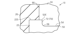
- FIG. 11 is a schematic cross-sectional view of an exemplary nitride semiconductor device according to the second embodiment, and is a diagram showing a case where the trench wall surface of the gate layer includes a vertical surface.
- FIG. 12 is a schematic cross-sectional view of an exemplary nitride semiconductor device according to the second embodiment, and is a diagram showing a case where the trench wall surface of the gate layer includes an inclined surface.
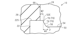
- FIG. 13 is a schematic cross-sectional view of an exemplary nitride semiconductor device according to the second embodiment, and is a diagram showing a case where the trench wall surface of the gate layer includes a gentler slope.
- FIG. 1 is a schematic cross-sectional view of an exemplary nitride semiconductor device 10 according to the first embodiment. First, with reference to FIG. 1, the overall structure of nitride semiconductor device 10 will be described below.
- the nitride semiconductor device 10 may be configured as a high electron mobility transistor (HEMT) using a nitride semiconductor such as gallium nitride (GaN), for example.
- the nitride semiconductor device 10 includes a substrate 12, a buffer layer 14 formed on the substrate 12, an electron transit layer 16 formed on the buffer layer 14, and an electron supply layer 18 formed on the electron transit layer 16. including.
- Substrate 12 may be formed of silicon (Si), silicon carbide (SiC), aluminum nitride (AlN), GaN, sapphire, or other substrate materials.
- the substrate 12 is a Si substrate.
- the thickness of the substrate 12 may be, for example, 200 ⁇ m or more and 1500 ⁇ m or less.
- the Z direction of the mutually orthogonal XYZ axes shown in FIG. 1 is a direction orthogonal to the main surface of the substrate 12.
- the term "planar view" used in this specification refers to viewing the nitride semiconductor device 10 from above along the Z direction, unless explicitly stated otherwise.
- the buffer layer 14 is located between the substrate 12 and the electron transit layer 16 and may be formed of any material that can alleviate the lattice mismatch between the substrate 12 and the electron transit layer 16.
- buffer layer 14 includes one or more nitride semiconductor layers.
- buffer layer 14 may include at least one of an AlN layer, an aluminum gallium nitride (AlGaN) layer, and a graded AlGaN layer having a different aluminum (Al) composition.
- the buffer layer 14 may be formed by a single AlN layer, a single AlGaN layer, a layer having an AlGaN/GaN superlattice structure, a layer having an AlN/AlGaN superlattice structure, or a layer having an AlN/GaN superlattice structure. can be formed.
- buffer layer 14 includes a first buffer layer formed on substrate 12 and a second buffer layer formed on the first buffer layer.
- the first buffer layer is, for example, an AlN layer, and may have a thickness of, for example, about 200 nm.
- the second buffer layer may include, for example, a plurality of AlGaN layers, and each AlGaN layer may have a thickness of, for example, about 100 nm.
- impurities may be introduced into a part of the buffer layer 14 to make it semi-insulating.
- the impurity is, for example, carbon (C) or iron (Fe), and the concentration of the impurity may be, for example, 4 ⁇ 10 16 cm ⁇ 3 or more.
- the electron transit layer 16 is made of a nitride semiconductor, and may be a GaN layer, for example.
- the electron transit layer 16 may have a thickness of, for example, 0.5 ⁇ m or more and 2 ⁇ m or less.
- impurities may be introduced into a part of the electron transit layer 16 to make the area other than the surface layer region of the electron transit layer 16 semi-insulating.
- the impurity is, for example, C
- the concentration of the impurity may be, for example, 1 ⁇ 10 19 cm ⁇ 3 or more in peak concentration.
- the electron supply layer 18 is made of a nitride semiconductor having a larger band gap than the electron transit layer 16, and may be an AlGaN layer, for example.
- the electron supply layer 18, which is an AlGaN layer has a larger band gap than the electron transit layer 16, which is a GaN layer.
- the electron supply layer 18 is made of Al x Ga 1-x N, and although not necessarily limited, x satisfies 0.1 ⁇ x ⁇ 0.4, more preferably 0.2 ⁇ x ⁇ 0. It is 3.
- the electron supply layer 18 may have a thickness of, for example, 5 nm or more and 20 nm or less.
- the electron transport layer 16 and the electron supply layer 18 are made of nitride semiconductors having different lattice constants. Therefore, the nitride semiconductor (eg, GaN) forming the electron transit layer 16 and the nitride semiconductor (eg, AlGaN) forming the electron supply layer 18 form a lattice-mismatched junction. Due to the spontaneous polarization of the electron transit layer 16 and the electron supply layer 18 and the piezo polarization caused by the stress applied to the heterojunction of the electron supply layer 18, electrons near the heterojunction interface between the electron transit layer 16 and the electron supply layer 18 are The energy level of the conduction band of the traveling layer 16 is lower than the Fermi level.
- two-dimensional electron gas (2DEG) 20 spreads within the electron transit layer 16 at a position close to the heterojunction interface between the electron transit layer 16 and the electron supply layer 18 (for example, at a distance of several nm from the interface). There is.
- the nitride semiconductor device 10 further includes a gate layer 22 formed on the electron supply layer 18, a gate electrode 24 formed on the gate layer 22, and a passivation layer 26. Passivation layer 26 covers electron supply layer 18 , gate layer 22 , and gate electrode 24 .
- the gate layer 22 is formed on the electron supply layer 18 using a nitride semiconductor containing acceptor type impurities.
- Gate layer 22 may be comprised of any material with a smaller bandgap than electron supply layer 18.
- the electron supply layer 18 is an AlGaN layer
- the gate layer 22 may be a GaN layer doped with acceptor type impurities, that is, a p-type GaN layer.
- the acceptor type impurity may include, for example, at least one of zinc (Zn), magnesium (Mg), and carbon (C).
- the acceptor type impurity may have a maximum concentration of, for example, 7 ⁇ 10 18 cm ⁇ 3 or more and 1 ⁇ 10 20 cm ⁇ 3 or less.
- the gate electrode 24 forms a Schottky junction with the gate layer 22.
- the gate electrode 24 is constituted by one or more metal layers, and may be, for example, a titanium nitride (TiN) layer.
- the gate electrode 24 may be composed of a first metal layer (for example, a Ti layer) and a second metal layer (for example, a TiN layer) provided on the first metal layer.
- the thickness of the gate electrode 24 from the upper surface 22S of the gate layer 22 to the upper surface of the gate electrode 24 may be, for example, 50 nm or more and 300 nm or less.
- the channel (2DEG 20) of the electron transport layer 16 disappears due to the presence of the acceptor type impurities contained in the gate layer 22. .
- a normally-off type nitride semiconductor HEMT is realized.
- the passivation layer 26 is made of, for example, a silicon nitride (SiN) film, a silicon dioxide (SiO 2 ) film, a silicon oxynitride (SiON) film, an alumina (Al 2 O 3 ) film, an AlN film, and an aluminum oxynitride (AlON) film. It is composed of a single film of any one of these or a composite film containing any combination of two or more thereof.
- the passivation layer 26 includes a first opening 26A that exposes the top surface of the electron supply layer 18 as a source connection region 18A, and a second opening 26B that exposes the top surface of the electron supply layer 18 as a drain connection region 18B.
- the gate layer 22 is located between the first opening 26A and the second opening 26B.
- the nitride semiconductor device 10 further includes a source electrode 32 and a drain electrode 34.
- the source electrode 32 is in contact with the source connection region 18A of the electron supply layer 18 through the first opening 26A of the passivation layer 26, and is in ohmic contact with the 2DEG 20 directly below the electron supply layer 18.
- the drain electrode 34 is in contact with the drain connection region 18B of the electron supply layer 18 through the second opening 26B of the passivation layer 26, and is in ohmic contact with the 2DEG 20 directly under the electron supply layer 18.
- the source electrode 32 and the drain electrode 34 are constituted by one or more metal layers using at least one of a Ti layer, a TiN layer, an Al layer, an AlSiCu layer, and an AlCu layer, for example.
- source electrode 32 and drain electrode 34 are formed of the same material.
- the gate layer 22 may have a step structure, although it is not necessarily limited to this structure.
- the gate layer 22 includes a ridge portion 42, and a source side extension portion 44 and a drain side extension portion 46 extending in opposite directions from both sides of the ridge portion 42.
- a step structure of the gate layer 22 is formed by the ridge portion 42, the source side extension portion 44, and the drain side extension portion 46.
- the ridge portion 42 corresponds to a relatively thick portion of the gate layer 22.
- the gate electrode 24 is in contact with the ridge portion 42 .
- the ridge portion 42 may have a rectangular or trapezoidal shape in a cross section taken along the XZ plane in FIG. 1 .
- the ridge portion 42 may have a thickness of, for example, 100 nm or more and 200 nm or less.
- the thickness of the ridge portion 42 is the distance from the top surface of the ridge portion 42 to the bottom surface (the bottom surface of the gate layer 22 in contact with the electron supply layer 18).
- the thickness of the ridge portion 42 (gate layer 22) can be determined in consideration of various parameters such as gate breakdown voltage.
- the source side extension portion 44 extends from the ridge portion 42 toward the first opening 26A of the passivation layer 26 (in the ⁇ X direction in FIG. 1).
- the drain side extension portion 46 extends from the ridge portion 42 toward the second opening 26B of the passivation layer 26 (in the +X direction in FIG. 1).
- the drain-side extension portion 46 extends longer from the ridge portion 42 than the source-side extension portion 44.
- the source side extension part 44 and the drain side extension part 46 may have the same length.
- the source side extension portion 44 may have a length of, for example, 0.2 ⁇ m or more and 0.3 ⁇ m or less in the direction from the ridge portion 42 toward the first opening 26A.
- the drain side extension portion 46 may have a length of, for example, 0.2 ⁇ m or more and 0.6 ⁇ m or less in the direction from the ridge portion 42 toward the second opening 26B.
- the source side extension part 44 and the drain side extension part 46 may have a thickness of, for example, 5 nm or more and 30 nm or less.
- a portion of the source electrode 32 is filled into the first opening 26A of the passivation layer 26, and a portion of the drain electrode 34 is filled into the second opening 26B of the passivation layer 26.
- the source electrode 32 is not necessarily limited to this configuration, it may include a source electrode portion 32A and a source field plate portion 32B continuous with the source electrode portion 32A.
- the source electrode section 32A includes a filling region that fills the first opening 26A, and an upper region that is formed integrally with the filling region and is located around the first opening 26A in plan view.
- the source field plate section 32B is formed integrally with the upper region of the source electrode section 32A, and includes the entire gate layer 22 (in the example of FIG. 1, the ridge section 42, the source side extension section 44, and the drain It is provided on the passivation layer 26 so as to cover all of the side extensions 46).
- the source field plate portion 32B has an end portion 32C near the drain electrode 34. This end portion 32C is located between the drain electrode 34 and the drain side extension portion 46 in plan view.
- the source field plate section 32B extends the depletion layer toward the 2DEG 20 directly below the source field plate section 32B when a high voltage is applied between the source and drain when the gate-source voltage is 0V. It plays a role of alleviating electric field concentration near the end of the gate electrode 24 and near the end of the gate layer 22.
- FIG. 2 is a partially enlarged cross-sectional view of the nitride semiconductor device 10 of FIG.
- the gate layer 22 includes a trench 50 recessed in the upper surface 22S of the gate layer 22 in a region in contact with the gate electrode 24.
- Trench 50 includes a trench opening end 52E, a trench bottom surface 54, and a curved surface 56 that is continuous with trench bottom surface 54 and curves from trench bottom surface 54 toward trench opening end 52E.
- the shape of the trench 50 is not particularly limited, in the example of FIG. 2, the trench 50 is formed into a bowl shape when viewed in cross section.
- the trench opening end 52E of the trench 50 includes a first end 52EA and a second end 52EB that face each other in the first direction.
- the first direction is the direction in which the source electrode 32 (first opening 26A), gate layer 22, and drain electrode 34 (second opening 26B) are lined up in FIG. 1, and corresponds to the X direction in FIG. do.
- the trench 50 has a trench width W1 corresponding to the distance between the first end 52EA and the second end 52EB in the first direction, and the curved surface 56 of the trench 50 extends from the trench bottom surface 54 to the first end 52EB. It includes a first curved surface 56A that curves toward the end 52EA, and a second curved surface 56B that curves from the trench bottom surface 54 toward the second end 52EB.
- the gate electrode 24 has a gate electrode length L1 in the first direction.
- the trench 50 (gate layer 22) and the gate electrode 24 are configured such that the trench width W1 is equal to or less than the gate electrode length L1.
- the gate electrode 24 includes an upper electrode part 62 and a lower electrode part 64.
- the lower electrode portion 64 corresponds to the lower region of the gate electrode 24 filled in the trench 50 .
- the upper electrode portion 62 is formed integrally with the lower electrode portion 64 and corresponds to an upper region of the gate electrode 24 located above the position of the upper surface 22S of the gate layer 22.
- the trench width W1 is less than the gate electrode length L1.
- the upper electrode portion 62 includes a protrusion 66 that protrudes laterally from the trench opening end 52E along the upper surface 22S of the gate layer 22.
- the protrusion 66 includes a first protrusion 66A that protrudes laterally along the upper surface 22S of the gate layer 22 from the first end 52EA of the trench opening end 52E, and a first protrusion 66A that protrudes laterally along the upper surface 22S of the gate layer 22 from the second end 52EB of the trench opening end 52E. 22, and a second protrusion 66B that protrudes laterally along the upper surface 22S of 22.
- the gate electrode 24 includes a first electrode end 24EA and a second electrode end 24EB that are in contact with the upper surface 22S of the gate layer 22.
- the electrode end part 24E corresponds to the lower end of the side surface 66SA of the first protrusion 66A
- the second electrode end 24EB corresponds to the lower end of the side surface 66SB of the second protrusion 66B.
- FIG. 3 is a partially enlarged sectional view of FIG. 2.
- FIG. 4 is a partially enlarged sectional view showing possible structures of the gate electrode 24.
- the trench 50 has a depth D1
- the first curved surface 56A (curved surface 56) has a radius of curvature R1.
- FIG. 3 shows the first curved surface 56A, the same applies to the second curved surface 56B.
- the depth D1 corresponds to the distance from the trench opening end 52E to the trench bottom surface 54 in the direction perpendicular to the upper surface 22S of the gate layer 22.
- the upper electrode portion 62 of the gate electrode 24 has a first protrusion that protrudes laterally along the upper surface 22S of the gate layer 22 from the first end 52EA of the trench opening end 52E with a protrusion width W2. 66A. Therefore, the gate electrode 24 includes a first electrode end 24EA (electrode end 24E) that is in contact with the upper surface 22S of the gate layer 22.
- FIG. 3 shows the first protrusion 66A, the same applies to the second protrusion 66B.
- the depth D1 of the trench 50, the radius of curvature R1 of the curved surface 56, and the protrusion width W2 of the protrusion 66 are set to values that can alleviate local electric field concentration on the gate layer 22 by a combination of these parameters. obtain.
- the values of depth D1, radius of curvature R1, and protrusion width W2 are selected to provide a higher electric field relaxation effect than when using a typical gate layer without a trench structure. Note that the electric field relaxation effect when using the gate layer 22 having a trench structure (the trench 50 including the curved surface 56) will be described later.
- the depth D1 may be, for example, 10 nm or more and 50 nm or less
- the radius of curvature R1 may be, for example, 5 nm or more and 30 nm or less
- the protrusion width W2 may be, for example, greater than 0 and 100 nm or less.
- the depth D1, the radius of curvature R1, and the protrusion width W2 are not necessarily limited to these ranges, and may be set to other ranges in which the electric field relaxation effect can be obtained.
- FIG. 4 shows a structure in which the protrusion width W2 of the protrusion 66 is 0 nm (that is, when the gate electrode 24 does not include the protrusion 66). In this way, the gate electrode 24 does not need to include the protrusion 66.
- the side surface 62S of the upper electrode section 62 is flat and continuous with the outer surface 64S of the lower electrode section 64 at the trench opening end 52E (first end 52EA in FIG. 4). Therefore, the gate electrode 24 in FIG. 4 does not include the electrode end portion 24E of the gate electrode 24 in FIG.
- FIG. 5 is a diagram showing simulation results of the electric field distribution (equipotential lines) around the gate electrode 24 of the nitride semiconductor device 10 of FIG. 1. Note that the structure in FIG. 5 corresponds to the structure in FIG. 3. This simulation result shows the electric field distribution when a gate voltage of, for example, 10 V is applied to the gate electrode 24. As shown in FIG. 5, in the structure of the gate layer 22 having the trench 50, the electric field (equipotential line) is concentrated in the region F1 of the curved surface 56 of the trench 50 (first curved surface 56A in FIG. 5). .
- FIG. 6 is a diagram showing simulation results of the electric field distribution (equipotential lines) around the gate electrode 240 of a typical nitride semiconductor device 100 including a gate layer 220 without a trench structure. Note that the structure in FIG. 6 is shown as a comparative example with the structure in FIG. 5.
- Gate layer 220 includes a flat top surface 220S and does not have trench 50 as in FIG.
- the gate electrode 240 is provided on the upper surface 220S of the gate layer 220, and includes an electrode end 240E (first electrode end 240EA in FIG. 6) in contact with the upper surface 220S.
- the electric field is locally concentrated in the region F2 of the gate layer 220 near the electrode end 240E of the gate electrode 240. ing.
- the electric field applied to the gate layer 22 is relaxed compared to the structure of FIG. 6.
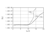
- FIG. 7 is a graph showing the gate breakdown voltage characteristics of the nitride semiconductor device 10 of FIG. 1 and the gate breakdown voltage characteristics of the nitride semiconductor device 100 of FIG. 6.
- a solid line graph 10L1 shows the gate breakdown voltage characteristics of the nitride semiconductor device 10
- a broken line graph 100L1 shows the gate breakdown voltage characteristics of the nitride semiconductor device 100.
- the horizontal axis represents the gate voltage Vg
- the vertical axis represents the gate current Ig.
- FIG. 8 is a graph showing the maximum electric field strength of the nitride semiconductor device 10 of FIG. 1 and the maximum electric field strength of the nitride semiconductor device 100 of FIG. 6.
- a solid line graph 10L2 indicates the maximum electric field intensity of the nitride semiconductor device 10
- a broken line graph 100L2 indicates the maximum electric field intensity of the nitride semiconductor device 100.
- the maximum electric field strength used in the present disclosure refers to the electric field strength at a location where the maximum electric field is applied.
- the two graphs 10L2 and 100L2 show that the maximum electric field strength (that is, the maximum applied electric field) is reduced in the nitride semiconductor device 10 of FIG. 1 compared to the nitride semiconductor device 100 of FIG. 6. .
- the maximum electric field is applied to the region F2 (near the electrode end 240E) of the gate layer 220 where the electric field is locally concentrated. Therefore, the graph 100L2 shows the electric field strength in the region F2 (near the electrode end 240E).
- the maximum electric field is applied to the region F1 (see FIG. 5) of the curved surface 56. Therefore, the graph 10L2 shows the electric field strength in the region F1 of the curved surface 56.
- the electric field applied to the gate layer 22 is dispersed and local electric field concentration is alleviated. As a result, in the nitride semiconductor device 10 of FIG. 1, the maximum electric field strength is reduced.
- the maximum electric field applied to the nitride semiconductor device 100 is approximately 5.69
- the maximum electric field applied to the nitride semiconductor device 10 is approximately 5.69
- the electric field is approximately 4.50. Therefore, an electric field relaxation effect is obtained.
- FIG. 9 shows the protrusion width W2 (see FIG. 3) of the protrusion 66 of the gate electrode 24, the depth D1 (see FIG. 3) of the trench 50, and the maximum electric field strength (the curved surface 56) in the nitride semiconductor device 10 of FIG. 2 is a graph showing the relationship between the maximum electric field applied to
- the example in FIG. 9 shows the relationship between the protrusion width W2 of the protrusion 66 and the maximum electric field applied to the curved surface 56 for three trenches 50 having depths D1 of 10 nm, 30 nm, and 50 nm, respectively.
- the gate voltage Vg is, for example, 10V.
- the protrusion width W2 is changed to, for example, 0 nm, 25 nm, 50 nm, 75 nm, 100 nm, 200 nm, and 250 nm.
- the reference value Ref indicates the maximum electric field strength of the nitride semiconductor device 100 in FIG. 6, that is, the maximum electric field (approximately 5.69) applied to the region F2 near the electrode end 240E.
- the maximum electric field strength becomes lower than the reference value Ref at a protrusion width W2 of 100 nm or less.
- the maximum electric field strength becomes lower than the reference value Ref regardless of the protrusion width W2.
- the protrusion width W2 is 100 nm or less, the maximum electric field strength will be lower than the reference value Ref regardless of the depth D1 of the trench 50.
- the gate electrode 24 includes the protrusion 66, the electric field relaxation effect is exhibited as long as the protrusion width W2 is greater than 0 and less than or equal to 100 nm, and the depth D1 is greater than or equal to 10 nm and less than or equal to 50 nm.
- the graph in FIG. 9 shows that the smaller the protrusion width W2, the greater the electric field relaxation effect. This is because as the protrusion width W2 increases, the distance between the electrode end 24E and the curved surface 56 increases, making it impossible to obtain a sufficient effect of alleviating electric field concentration near the electrode end 24E.
- the depth D1 is small, for example, when the depth D1 is 10 nm, the electric field relaxation effect is smaller than when the depth D1 is 30 nm or 50 nm. This is because the effect of widely dispersing the electric field using the curved surface 56 of the trench 50 is reduced. Therefore, the depth D1 is more preferably 30 nm or more and 50 nm or less.
- the maximum electric field strength is the highest regardless of whether the depth D1 of the trench 50 is 10 nm, 30 nm, or 50 nm. It gets lower. Therefore, by combining the structure of the gate electrode 24 shown in FIG. 4 described above with the trench structure of the gate layer 22, the maximum electric field relaxation effect can be obtained. Therefore, it is preferable that the gate electrode 24 has the structure shown in FIG. 4 rather than the structure shown in FIG.
- FIG. 10 shows the protrusion width W2 (see FIG. 3) of the protrusion 66 of the gate electrode 24, the radius of curvature R1 (see FIG. 3) of the curved surface 56, and the maximum electric field strength (see FIG. 3) in the nitride semiconductor device 10 of FIG. 56 is a graph showing the relationship between the maximum electric field applied to the
- the example in FIG. 10 shows the relationship between the protrusion width W2 of the protrusion 66 and the maximum electric field applied to the curved surface 56 for four trenches 50 in which the curved surface 56 has a radius of curvature R1 of 5 nm, 10 nm, 20 nm, and 30 nm, respectively. It shows a relationship.
- the gate voltage Vg is, for example, 10V.
- the protrusion width W2 is varied, for example, from 0 nm to 50 nm to 100 nm.
- the reference value Ref indicates the maximum electric field strength of the nitride semiconductor device 100 of FIG. 6, that is, the maximum electric field (approximately 5.69) applied to the region F2 near the electrode end 240E. There is.
- the maximum electric field strength becomes lower than the reference value Ref at a protrusion width W2 of 40 nm or less.
- the radius of curvature R1 is 10 nm, 20 nm, and 30 nm, the maximum electric field strength is lower than the reference value Ref regardless of the protrusion width W2. Therefore, when the gate electrode 24 includes the protrusion 66, the electric field relaxation effect is exhibited as long as the protrusion width W2 is greater than 0 and less than or equal to 100 nm, and the radius of curvature R1 is greater than or equal to 10 nm and less than or equal to 30 nm.
- the electric field relaxation effect is exhibited if the protrusion width W2 is greater than 0 and less than or equal to 40 nm, and the radius of curvature R1 is greater than or equal to 5 nm and less than or equal to 30 nm.
- FIG. 10 also shows that the smaller the protrusion width W2, the greater the electric field relaxation effect. This is because, as described above, when the protrusion width W2 increases, the distance between the electrode end 24E and the curved surface 56 increases, making it impossible to obtain a sufficient effect of alleviating electric field concentration near the electrode end 24E. It's for a reason. Further, when the radius of curvature R1 is small, for example, when the radius of curvature R1 is 5 nm, the electric field relaxation effect is smaller than when the radius of curvature R1 is 10 nm, 20 nm, or 30 nm. This is because when the curvature of the curved surface 56 is small, the electric field concentration on the curved surface 56 becomes large. Therefore, the radius of curvature R1 is more preferably 10 nm or more and 30 nm or less.
- Gate layer 22 of nitride semiconductor device 10 includes a trench 50 recessed in upper surface 22S of gate layer 22 in a region in contact with gate electrode 24.
- Trench 50 includes a curved surface 56 that curves from trench bottom surface 54 toward trench opening end 52E.
- the electric field is concentrated on a wider curved surface 56 of the trench 50, thereby suppressing local electric field concentration in the gate layer 22 near the electrode end 24E of the gate electrode 24.
- the electric field applied to the gate layer 22 is relaxed.
- the gate electrode 24 does not include the protrusion 66
- the gate electrode 24 does not include the electrode end portion 24E in contact with the upper surface 22S of the gate layer 22. Therefore, the electric field applied to the gate layer 22 is further relaxed.
- the nitride semiconductor device 10 of the first embodiment has the following advantages.
- (1-1) The gate layer 22 has a trench 50 including a curved surface 56. With this structure, the electric field can be concentrated over a wider range of curved surface 56 of trench 50. Thereby, local electric field concentration in the portion of the gate layer 22 near the electrode end 24E of the gate electrode 24 can be suppressed, and the electric field (maximum electric field strength) applied to the gate layer 22 can be relaxed. As a result, it is possible to suppress crystal defects in the gate layer that may occur due to local electric field concentration, as well as crystal destruction, and to suppress a decrease in gate breakdown voltage.
- the trench width W1 of the trench 50 is less than or equal to the gate electrode length L1 of the gate electrode 24 (see FIG. 2).
- the gate electrode 24 includes a lower electrode portion 64 filled in the trench 50 and an upper electrode portion 62 formed integrally with the lower electrode portion 64 and located above the top surface position of the gate layer 22. include.
- the gate electrode 24 may be configured such that the side surface 62S of the upper electrode section 62 includes a side surface 62S that is flat and continuous with the outer surface 64S of the lower electrode section 64 at the position of the trench opening end 52E (see FIG. 4).
- gate electrode 24 does not include protrusion 66 (see FIG. 3) and electrode end 24E (see FIG. 3).
- the upper electrode portion 62 may include a protrusion 66 that protrudes laterally from the trench opening end 52E along the upper surface 22S of the gate layer 22 (see FIG. 3). Even with such a structure of the gate electrode 24, the electric field applied to the gate layer 22 can be relaxed by using the gate layer 22 having the trench 50 including the curved surface 56.
- the protrusion 66 may protrude laterally from the trench opening end 52E along the upper surface 22S of the gate layer 22 with a protrusion width W2 that is less than or equal to the depth D1 of the trench 50. If the protrusion width W2 is large, the distance between the electrode end 24E and the curved surface 56 becomes large, so that the effect of alleviating electric field concentration near the electrode end 24E may not be sufficiently obtained. Since the protrusion width W2 is limited according to the depth D1 by satisfying the relationship W2 ⁇ D1, the electric field relaxation effect can be maintained satisfactorily.
- the protrusion width W2 of the protrusion 66 may be greater than 0 nm and less than or equal to 100 nm.
- the electric field relaxation effect is exhibited (see FIG. 9).
- the radius of curvature R1 of the curved surface 56 is exhibited (see FIG. 10). As shown in FIGS.
- the electron transit layer 16 may be a GaN layer.
- the electron supply layer 18 may be an AlGaN layer.
- the gate layer 22 may be a GaN layer containing acceptor type impurities. With this structure, it is possible to reduce the electric field (maximum electric field strength) applied to the gate layer 22 in a normally-off type GaN-HEMT, thereby suppressing a decrease in gate breakdown voltage.
- FIGS. 11 to 13 are schematic cross-sectional views of an exemplary nitride semiconductor device 10 according to the second embodiment. Note that in FIGS. 11 to 13, the same reference numerals are given to the same components as those of the nitride semiconductor device 10 according to the first embodiment. In the following, descriptions of components similar to those in the first embodiment will be omitted, and components different from those in the first embodiment will be described.
- the trench 50 includes a trench wall surface 70 that connects the trench opening end 52E and the curved surface 56.
- trench wall surface 70 includes a vertical surface 72 perpendicular to upper surface 22S of gate layer 22.
- the trench wall surface 70 includes an inclined surface 74 inclined with respect to the upper surface 22S of the gate layer 22.
- sloped surface 74 has an inclination angle of 60 degrees
- sloped surface 74 has a more gradual slope angle of 30 degrees.
- the slope 74 may be arbitrarily selected to be greater than 0° and less than 90°, but is preferably greater than or equal to 30° and less than or equal to 60°.
- the trench wall surface 70 may include a second curved surface 76 in addition to the inclined surface 74.
- the second curved surface 76 connects the inclined surface 74 and the trench opening end 52E.
- the second curved surface 76 can also have the effect of dispersing the electric field applied to the gate layer 22 and mitigating local electric field concentration.
- trench wall surface 70 may include only sloped surface 74.
- the trench 50 includes the trench wall surface 70 between the trench opening end 52E and the curved surface 56, the depth D1 of the trench 50 (see FIG. 3) and the radius of curvature R1 of the curved surface 56 (see FIG. 3) can be set as desired. It becomes easier to form the value of .
- the protrusion width W2 of the protrusion 66 is determined from the connection point P between the curved surface 56 and the trench bottom surface 54 to the trench opening end in a plan view.
- the distance W3 across the curved surface 56 up to 52E may be less than or equal to W3.
- the trench 50 in FIG. 13 may also be formed to satisfy the relationship W2 ⁇ W3.
- the trench 50 in FIG. 11 or the trench 50 in the first embodiment may also be formed to satisfy the relationship W2 ⁇ W3.
- Table 1 below shows the maximum force applied to the curved surface 56 when the protrusion width W2 of the protrusion 66 and the depth D1 of the trench 50 are changed in the trench 50 of FIG.
- the gate voltage is, for example, 10V
- the protrusion width W2 is varied between 0 nm, 50 nm, and 100 nm
- the depth D1 is varied between 10 nm, 30 nm, and 50 nm.
- the radius of curvature R1 of the curved surface 56 is, for example, 5 nm.
- Table 2 also shows that in the trench 50 of FIG. 12 which includes the slope 74 with an inclination angle of 60° as the trench wall surface 70, the protrusion width W2 of the protrusion 66 and the depth D1 of the trench 50 are changed under the same conditions as in Table 1.
- the figure shows an example in which the maximum electric field applied to the curved surface 56 was measured when the curved surface 56 was bent.
- Table 3 shows that in the trench 50 of FIG. 13 which includes the slope 74 with an inclination angle of 30° as the trench wall surface 70, the protrusion width W2 of the protrusion 66 and the depth D1 of the trench 50 are changed under the same conditions as Table 1.
- the figure shows an example in which the maximum electric field applied to the curved surface 56 was measured when the curved surface 56 was bent.
- Tables 1 to 1 The maximum electric field shown in Fig. 3 is lower than the reference value Ref when the protrusion width W2 is 0 nm. Further, depending on the combination of the protrusion width W2 and the depth D1, the maximum electric field becomes lower than the reference value Ref.
- the maximum electric field is lower when the slope is on the inclined surface 74 than when it is on the vertical surface 72, and the maximum electric field is lower when the slope angle of the slope 74 is 30° compared to when the slope is at 60°.
- the maximum electric field is lower when the slope angle of the slope 74 is 30° compared to when the slope is at 60°.
- the nitride semiconductor device 10 is configured as a normally-off type nitride semiconductor HEMT, but it may also be configured as a normally-on type nitride semiconductor HEMT.
- the nitride semiconductor device 10 is configured as a HEMT using gallium nitride, but it may be configured as a HEMT using other group III nitride semiconductors.
- the radius of curvature R1 of the curved surface 56 can also be changed as appropriate.
- the term “on” as used in this disclosure includes the meanings of “on” and “above” unless the context clearly indicates otherwise.
- the phrase “the first layer is formed on the second layer” refers to the fact that in some embodiments the first layer may be directly disposed on the second layer in contact with the second layer, but in other embodiments. It is contemplated that the first layer may be placed above the second layer without contacting the second layer. That is, the term “on” does not exclude structures in which other layers are formed between the first layer and the second layer.
- an intermediate layer for example, a spacer layer
- the electron supply layer 18 is formed on the electron transit layer 16
- an intermediate layer for example, a spacer layer
- the Z-axis direction used in the present disclosure does not necessarily have to be a vertical direction, nor does it need to completely coincide with the vertical direction. Accordingly, in various structures according to the present disclosure (e.g., the structure shown in FIG. 1), “upper” and “lower” in the Z-axis direction described herein are “upper” and “lower” in the vertical direction. Not limited to one thing.
- the X-axis direction may be a vertical direction
- the Y-axis direction may be a vertical direction.
- Appendix A1 an electron transit layer (16) made of a nitride semiconductor; A nitride semiconductor disposed on the electron transit layer (16) and having a larger band gap than the electron transit layer (16) to generate a two-dimensional electron gas (20) in the electron transit layer (16).
- the gate layer (22) includes a trench (50) recessed in the upper surface (22S) of the gate layer (22) in a region in contact with the gate electrode (24),
- the trench (50) is a trench opening end (52E), a trench bottom (54); a curved surface (56:56A; 56B) that is continuous with the trench bottom surface (54) and curves from the trench bottom surface (54) toward the trench opening end (52E);
- a nitride semiconductor device (10) comprising:
- the trench opening end (52E) includes a first end (52EA) and a second end (52EB) that face each other in the first direction,
- the trench (50) has a trench width (W1) corresponding to the distance between the first end (52EA) and the second end (52EB) in the first direction,
- the gate electrode (24) has a gate electrode length (L1) in the first direction,
- the gate electrode (24) is a lower electrode portion (64) filled in the trench (50); an upper electrode part (62) formed integrally with the lower electrode part (64) and located above the upper surface position of the gate layer (22);
- the upper electrode part (62) includes a side surface (62S) that is flat and continuous with the outer surface (64S) of the lower electrode part (64) at the position of the trench opening end (52E), according to appendix A1 or A2.
- the gate electrode (24) is a lower electrode portion (64) filled in the trench (50); an upper electrode part (62) formed integrally with the lower electrode part (64) and located above the upper surface position of the gate layer (22);
- the upper electrode portion (62) includes a protrusion (66:66A; 66B) that protrudes laterally from the trench opening end (52E) along the upper surface of the gate layer (22), as described in Appendix A1 or A2.
- the protrusion (66:66A; 66B) extends from the trench opening end (52E) along the upper surface of the gate layer (22) with a protrusion width (W2) equal to or less than the depth (D1) of the trench (50).
- the protrusion width (W2) is defined as the width of the curved surface (56) from the connection point (P) between the curved surface (56:56A; 56B) and the trench bottom surface (54) to the trench opening end (52E) in plan view. 56A;
- the protrusion (66:66A; 66B) protrudes laterally from the trench opening end (52E) along the upper surface of the gate layer (22) with a protrusion width (W2) of greater than 0 nm and less than or equal to 100 nm. , the nitride semiconductor device (10) according to appendix A4.
- the trench (50) includes a trench wall surface (70) connecting the trench opening end (52E) and the curved surface (56:56A; 56B), as described in any one of Appendices A1 to A6.
- the electron transit layer (16) is a GaN layer
- the electron supply layer (18) is an AlGaN layer.
- the nitride semiconductor device (10) according to any one of appendices A1 to A15, wherein the gate layer (22) is a GaN layer containing the acceptor type impurity.
Landscapes
- Junction Field-Effect Transistors (AREA)
Priority Applications (2)
| Application Number | Priority Date | Filing Date | Title |
|---|---|---|---|
| JP2024511458A JPWO2023189039A1 (https=) | 2022-03-30 | 2023-02-22 | |
| US18/895,404 US20250015136A1 (en) | 2022-03-30 | 2024-09-25 | Nitride semiconductor device |
Applications Claiming Priority (2)
| Application Number | Priority Date | Filing Date | Title |
|---|---|---|---|
| JP2022-057076 | 2022-03-30 | ||
| JP2022057076 | 2022-03-30 |
Related Child Applications (1)
| Application Number | Title | Priority Date | Filing Date |
|---|---|---|---|
| US18/895,404 Continuation US20250015136A1 (en) | 2022-03-30 | 2024-09-25 | Nitride semiconductor device |
Publications (1)
| Publication Number | Publication Date |
|---|---|
| WO2023189039A1 true WO2023189039A1 (ja) | 2023-10-05 |
Family
ID=88200551
Family Applications (1)
| Application Number | Title | Priority Date | Filing Date |
|---|---|---|---|
| PCT/JP2023/006474 Ceased WO2023189039A1 (ja) | 2022-03-30 | 2023-02-22 | 窒化物半導体装置 |
Country Status (3)
| Country | Link |
|---|---|
| US (1) | US20250015136A1 (https=) |
| JP (1) | JPWO2023189039A1 (https=) |
| WO (1) | WO2023189039A1 (https=) |
Citations (7)
| Publication number | Priority date | Publication date | Assignee | Title |
|---|---|---|---|---|
| JP2007194411A (ja) * | 2006-01-19 | 2007-08-02 | Sanyo Electric Co Ltd | スイッチ集積回路装置およびその製造方法 |
| JP2007534163A (ja) * | 2004-01-23 | 2007-11-22 | インターナショナル・レクチファイヤー・コーポレーション | エンハンスメント型iii族窒化物デバイス |
| JP2008091392A (ja) * | 2006-09-29 | 2008-04-17 | Matsushita Electric Ind Co Ltd | 窒化物半導体装置及びその製造方法 |
| JP2008306083A (ja) * | 2007-06-11 | 2008-12-18 | Nec Corp | Iii−v族窒化物半導体電界効果型トランジスタおよびその製造方法 |
| JP2010165987A (ja) * | 2009-01-19 | 2010-07-29 | Panasonic Corp | 半導体装置及びその製造方法 |
| WO2012172753A1 (ja) * | 2011-06-13 | 2012-12-20 | パナソニック株式会社 | 半導体装置及びその製造方法 |
| WO2018230136A1 (ja) * | 2017-06-13 | 2018-12-20 | パナソニックIpマネジメント株式会社 | 窒化物半導体装置及びその製造方法 |
-
2023
- 2023-02-22 JP JP2024511458A patent/JPWO2023189039A1/ja active Pending
- 2023-02-22 WO PCT/JP2023/006474 patent/WO2023189039A1/ja not_active Ceased
-
2024
- 2024-09-25 US US18/895,404 patent/US20250015136A1/en active Pending
Patent Citations (7)
| Publication number | Priority date | Publication date | Assignee | Title |
|---|---|---|---|---|
| JP2007534163A (ja) * | 2004-01-23 | 2007-11-22 | インターナショナル・レクチファイヤー・コーポレーション | エンハンスメント型iii族窒化物デバイス |
| JP2007194411A (ja) * | 2006-01-19 | 2007-08-02 | Sanyo Electric Co Ltd | スイッチ集積回路装置およびその製造方法 |
| JP2008091392A (ja) * | 2006-09-29 | 2008-04-17 | Matsushita Electric Ind Co Ltd | 窒化物半導体装置及びその製造方法 |
| JP2008306083A (ja) * | 2007-06-11 | 2008-12-18 | Nec Corp | Iii−v族窒化物半導体電界効果型トランジスタおよびその製造方法 |
| JP2010165987A (ja) * | 2009-01-19 | 2010-07-29 | Panasonic Corp | 半導体装置及びその製造方法 |
| WO2012172753A1 (ja) * | 2011-06-13 | 2012-12-20 | パナソニック株式会社 | 半導体装置及びその製造方法 |
| WO2018230136A1 (ja) * | 2017-06-13 | 2018-12-20 | パナソニックIpマネジメント株式会社 | 窒化物半導体装置及びその製造方法 |
Non-Patent Citations (1)
| Title |
|---|
| ZHANG WEIHANG, LIU XI, FU LIYU, HUANG REN, ZHAO SHENGLEI, ZHANG JINCHENG, ZHANG JINFENG, HAO YUE: "Investigation of normally-off GaN-based p-channel and n-channel heterojunction field-effect transistors for monolithic integration", RESULTS IN PHYSICS, ELSEVIER BV, NL, vol. 24, 1 May 2021 (2021-05-01), NL , pages 104209, XP093096427, ISSN: 2211-3797, DOI: 10.1016/j.rinp.2021.104209 * |
Also Published As
| Publication number | Publication date |
|---|---|
| JPWO2023189039A1 (https=) | 2023-10-05 |
| US20250015136A1 (en) | 2025-01-09 |
Similar Documents
| Publication | Publication Date | Title |
|---|---|---|
| US10998433B2 (en) | Semiconductor device | |
| US7491983B2 (en) | Nitride-based semiconductor device of reduced current leakage | |
| JP5691267B2 (ja) | 半導体装置 | |
| US20140110759A1 (en) | Semiconductor device | |
| US10158012B1 (en) | Semiconductor device | |
| JP7021038B2 (ja) | 半導体装置 | |
| JP6649208B2 (ja) | 半導体装置 | |
| US20150263155A1 (en) | Semiconductor device | |
| US12119396B2 (en) | Semiconductor device | |
| JP2007180143A (ja) | 窒化物半導体素子 | |
| CN103003930B (zh) | 场效应晶体管 | |
| JP2008130655A (ja) | 半導体素子 | |
| CN114566535A (zh) | 一种半导体器件及其制备方法 | |
| JP2019096720A (ja) | 半導体装置、電源回路、及び、コンピュータ | |
| JP2009278028A (ja) | 半導体装置 | |
| US20250040212A1 (en) | Nitride semiconductor device | |
| WO2023189039A1 (ja) | 窒化物半導体装置 | |
| WO2023176373A1 (ja) | 半導体装置 | |
| US20240128366A1 (en) | Nitride semiconductor device | |
| US20240290825A1 (en) | Semiconductor device | |
| JP2023146620A (ja) | 窒化物半導体装置 | |
| US20240282826A1 (en) | Nitride semiconductor device | |
| JP2013183034A (ja) | 電力用半導体装置 | |
| JP5697046B2 (ja) | 高移動度電界効果トランジスタ | |
| JP2024012856A (ja) | 窒化物半導体装置 |
Legal Events
| Date | Code | Title | Description |
|---|---|---|---|
| 121 | Ep: the epo has been informed by wipo that ep was designated in this application |
Ref document number: 23779069 Country of ref document: EP Kind code of ref document: A1 |
|
| ENP | Entry into the national phase |
Ref document number: 2024511458 Country of ref document: JP Kind code of ref document: A |
|
| NENP | Non-entry into the national phase |
Ref country code: DE |
|
| 122 | Ep: pct application non-entry in european phase |
Ref document number: 23779069 Country of ref document: EP Kind code of ref document: A1 |