WO2023188965A1 - 半導体装置、モジュール - Google Patents
半導体装置、モジュール Download PDFInfo
- Publication number
- WO2023188965A1 WO2023188965A1 PCT/JP2023/005650 JP2023005650W WO2023188965A1 WO 2023188965 A1 WO2023188965 A1 WO 2023188965A1 JP 2023005650 W JP2023005650 W JP 2023005650W WO 2023188965 A1 WO2023188965 A1 WO 2023188965A1
- Authority
- WO
- WIPO (PCT)
- Prior art keywords
- current
- signal
- terminal
- resistor
- input
- Prior art date
- Legal status (The legal status is an assumption and is not a legal conclusion. Google has not performed a legal analysis and makes no representation as to the accuracy of the status listed.)
- Ceased
Links
Images








Classifications
-
- H—ELECTRICITY
- H02—GENERATION; CONVERSION OR DISTRIBUTION OF ELECTRIC POWER
- H02M—APPARATUS FOR CONVERSION BETWEEN AC AND AC, BETWEEN AC AND DC, OR BETWEEN DC AND DC, AND FOR USE WITH MAINS OR SIMILAR POWER SUPPLY SYSTEMS; CONVERSION OF DC OR AC INPUT POWER INTO SURGE OUTPUT POWER; CONTROL OR REGULATION THEREOF
- H02M3/00—Conversion of DC power input into DC power output
- H02M3/02—Conversion of DC power input into DC power output without intermediate conversion into AC
- H02M3/04—Conversion of DC power input into DC power output without intermediate conversion into AC by static converters
- H02M3/10—Conversion of DC power input into DC power output without intermediate conversion into AC by static converters using discharge tubes with control electrode or semiconductor devices with control electrode
- H02M3/145—Conversion of DC power input into DC power output without intermediate conversion into AC by static converters using discharge tubes with control electrode or semiconductor devices with control electrode using devices of a triode or transistor type requiring continuous application of a control signal
- H02M3/155—Conversion of DC power input into DC power output without intermediate conversion into AC by static converters using discharge tubes with control electrode or semiconductor devices with control electrode using devices of a triode or transistor type requiring continuous application of a control signal using semiconductor devices only
- H02M3/156—Conversion of DC power input into DC power output without intermediate conversion into AC by static converters using discharge tubes with control electrode or semiconductor devices with control electrode using devices of a triode or transistor type requiring continuous application of a control signal using semiconductor devices only with automatic control of output voltage or current, e.g. switching regulators
- H02M3/158—Conversion of DC power input into DC power output without intermediate conversion into AC by static converters using discharge tubes with control electrode or semiconductor devices with control electrode using devices of a triode or transistor type requiring continuous application of a control signal using semiconductor devices only with automatic control of output voltage or current, e.g. switching regulators including plural semiconductor devices as final control devices for a single load
-
- H—ELECTRICITY
- H05—ELECTRIC TECHNIQUES NOT OTHERWISE PROVIDED FOR
- H05B—ELECTRIC HEATING; ELECTRIC LIGHT SOURCES NOT OTHERWISE PROVIDED FOR; CIRCUIT ARRANGEMENTS FOR ELECTRIC LIGHT SOURCES, IN GENERAL
- H05B45/00—Circuit arrangements for operating light-emitting diodes [LED]
- H05B45/10—Controlling the intensity of the light
- H05B45/14—Controlling the intensity of the light using electrical feedback from LEDs or from LED modules
-
- H—ELECTRICITY
- H02—GENERATION; CONVERSION OR DISTRIBUTION OF ELECTRIC POWER
- H02M—APPARATUS FOR CONVERSION BETWEEN AC AND AC, BETWEEN AC AND DC, OR BETWEEN DC AND DC, AND FOR USE WITH MAINS OR SIMILAR POWER SUPPLY SYSTEMS; CONVERSION OF DC OR AC INPUT POWER INTO SURGE OUTPUT POWER; CONTROL OR REGULATION THEREOF
- H02M1/00—Details of apparatus for conversion
- H02M1/0003—Details of control, feedback or regulation circuits
- H02M1/0009—Devices or circuits for detecting current in a converter
-
- H—ELECTRICITY
- H02—GENERATION; CONVERSION OR DISTRIBUTION OF ELECTRIC POWER
- H02M—APPARATUS FOR CONVERSION BETWEEN AC AND AC, BETWEEN AC AND DC, OR BETWEEN DC AND DC, AND FOR USE WITH MAINS OR SIMILAR POWER SUPPLY SYSTEMS; CONVERSION OF DC OR AC INPUT POWER INTO SURGE OUTPUT POWER; CONTROL OR REGULATION THEREOF
- H02M1/00—Details of apparatus for conversion
- H02M1/32—Means for protecting converters other than automatic disconnection
-
- H—ELECTRICITY
- H05—ELECTRIC TECHNIQUES NOT OTHERWISE PROVIDED FOR
- H05B—ELECTRIC HEATING; ELECTRIC LIGHT SOURCES NOT OTHERWISE PROVIDED FOR; CIRCUIT ARRANGEMENTS FOR ELECTRIC LIGHT SOURCES, IN GENERAL
- H05B45/00—Circuit arrangements for operating light-emitting diodes [LED]
- H05B45/30—Driver circuits
- H05B45/37—Converter circuits
- H05B45/3725—Switched mode power supply [SMPS]
- H05B45/375—Switched mode power supply [SMPS] using buck topology
-
- H—ELECTRICITY
- H05—ELECTRIC TECHNIQUES NOT OTHERWISE PROVIDED FOR
- H05B—ELECTRIC HEATING; ELECTRIC LIGHT SOURCES NOT OTHERWISE PROVIDED FOR; CIRCUIT ARRANGEMENTS FOR ELECTRIC LIGHT SOURCES, IN GENERAL
- H05B45/00—Circuit arrangements for operating light-emitting diodes [LED]
- H05B45/40—Details of LED load circuits
Definitions
- the invention disclosed herein relates to semiconductor devices and modules.
- Patent Document 1 can be mentioned as an example of the conventional technology related to the above.
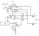
- the invention disclosed herein aims to provide a semiconductor device and a module with high current detection accuracy.
- the semiconductor device disclosed in this specification includes a current detection circuit configured to generate a current detection signal according to a current to be monitored, and an error between the current detection signal and a predetermined reference signal.
- an error amplifier configured to generate a corresponding error signal;
- a comparator configured to generate a set signal by comparing the error signal and the current detection signal; and
- a comparator configured to receive the input of the set signal.
- a controller configured to control the current to be monitored;
- the current detection circuit includes a current output type differential amplifier; and a connection between a first input terminal of the differential amplifier and a first current sense terminal.
- a first input resistor configured to be connected between the differential amplifier, a second input resistor configured to be connected between the second input terminal of the differential amplifier and the second current sense terminal; an output resistor configured to be connected to an output terminal of the differential amplifier; and a first configured to flow a first feedback current between the first input terminal and the output terminal of the differential amplifier. and a second feedback current path configured to flow a second feedback current between the second input terminal and the output terminal of the differential amplifier.
- the semiconductor device disclosed in this specification includes a current detection circuit configured to generate a current detection signal according to a current to be monitored, and an error between the current detection signal and a predetermined reference signal.
- an error amplifier configured to generate a corresponding error signal;
- a comparator configured to generate a set signal by comparing the error signal and the current detection signal; and
- a comparator configured to receive the input of the set signal.
- a controller configured to control the current to be monitored;
- the current detection circuit includes a current output type differential amplifier; and a connection between a first input terminal of the differential amplifier and a first current sense terminal.
- a first input resistor configured to be connected between a second input resistor configured to be connected between a second input terminal of the differential amplifier and a second current sense terminal; a VI converter configured to convert a signal into a current signal; a feedback resistor configured to determine a gain of the VI converter; and a first current sense terminal and a first current sense terminal of the VI converter.
- a first reference current path configured to flow a first reference current between the second current sense terminal and the second output terminal of the VI converter; a second reference current path configured to flow.
- FIG. 1 is a diagram showing a first embodiment of an LED lamp module.
- FIG. 2 is a diagram showing output feedback control using a bottom detection on-time fixed method.
- FIG. 3 is a diagram showing a second embodiment of the LED lamp module.
- FIG. 4 is a diagram showing the response performance required of the LED driver IC.
- FIG. 5 is a diagram showing a path of surge current flowing during a load open/shortcut test.
- FIG. 6 is a diagram showing the waveform of a surge current flowing during a load open/shortcut test.
- FIG. 7 is a diagram showing a third embodiment of the LED lamp module.
- FIG. 8 is a diagram showing the occurrence of gain error in the current sense amplifier.
- FIG. 9 is a diagram showing a fourth embodiment of the LED lamp module.
- FIG. 1 is a diagram showing a first embodiment of an LED lamp module.
- FIG. 2 is a diagram showing output feedback control using a bottom detection on-time fixed method.
- FIG. 3 is
- FIG. 10 is a diagram showing the temperature characteristics of the current detection signal.
- FIG. 11 is a diagram showing a fifth embodiment of the LED lamp module.
- FIG. 12 is a diagram showing the elimination of gain errors in the current sense amplifier.
- FIG. 13 is a diagram showing a sixth embodiment of the LED lamp module.
- FIG. 14 is a diagram equivalently showing the current detection circuit of the sixth embodiment.
- FIG. 15 is a diagram showing a seventh embodiment of the LED lamp module.
- FIG. 16 is a diagram showing an eighth embodiment of the LED lamp module.
- FIG. 17 is a diagram showing a ninth embodiment of the LED lamp module.
- FIG. 18 is a diagram showing a tenth embodiment of the LED lamp module.
- FIG. 19 is a diagram showing an example of signal transmission in the eighth embodiment.
- FIG. 20 is a diagram showing an eleventh embodiment of the LED lamp module.
- FIG. 21 is a diagram showing an example of signal transmission in the tenth embodiment.
- FIG. 1 is a diagram showing a first embodiment (basic configuration) of an LED lamp module.
- the LED driver IC1 is a semiconductor device that steps down the input voltage Vi of the power system and supplies power to the LED string 2. Note that the LED driver IC 1 has a plurality of external terminals (PIN pin, SW pin, BOOT pin, PGND pin, SNSP pin, SNSN pin, TON pin, and , COMP pin, etc.).
- the PIN pin is a power system power supply terminal.
- the SW pin is a switch output terminal.
- the BOOT pin is a bootstrap capacitor connection terminal for driving the upper gate.
- the PGND pin is a power system ground terminal.
- the SNSP pin is the first current sense terminal (+).
- the SNSN pin is the second current sense terminal (-).
- the TON pin is a resistor connection terminal for setting on-time.
- the COMP pin is a capacitor connection terminal for phase compensation.
- the PIN pin is connected to the power supply end of the power system (the end to which the input voltage Vi is applied).
- the SW pin is connected to the first end of inductor L1.
- a second end of the inductor L1 is connected to a first end of the sense resistor Rs.
- the second end of the sense resistor Rs is connected to the anode of the LED string 2.
- the cathode of the LED string 2 is connected to the ground end.
- a capacitor Cb bootsstrap capacitor
- a capacitor Co output capacitor
- a first end (high potential end) of the sense resistor Rs is connected to the SNSP pin.
- the second end (low potential end) of the sense resistor Rs is connected to the SNSN pin.
- the PGND pin is connected to the ground terminal of the power system.
- a resistor Rt on-time setting resistor
- a capacitor Cc phase compensation capacitor
- the LED driver IC 1 of this configuration example includes, as means for driving the LED string 2, an upper switch 11H, a lower switch 11L, an upper driver 12H, a lower driver 12L, a controller 13, and an on-time setting section. 14, a slope signal generation section 15, a current sense amplifier 16, an error amplifier 17, a comparator 18, a DAC 19, and a bootstrap diode D1.
- components other than those described above may be integrated in the LED driver IC1.
- the upper switch 11H is connected between the PIN pin and the SW pin, and is turned on/off according to the upper gate signal GH.
- an NMOSFET N-channel type metal oxide semiconductor field effect transistor
- PMOSFET P-channel type MOSFET
- the bootstrap diode D1, capacitor Cb, and BOOT pin become unnecessary.
- the lower switch 11L is connected between the SW pin and the PGND pin, and is turned on/off according to the lower gate signal GL.
- the upper switch 11H and lower switch 11L connected in this way form a half-bridge output stage that outputs a rectangular waveform switch voltage Vsw from the SW pin. That is, the upper switch 11H corresponds to an output element, and the lower switch 11L corresponds to a synchronous rectifier. Note that the previously mentioned inductor L1, sense resistor Rs, and LED string 2 are connected in series to the upper switch 11H. Further, in this figure, a synchronous rectification type half-bridge output stage is shown, but if a diode rectification type is adopted, a diode may be used as the lower switch 11L.
- the upper driver 12H generates the upper gate signal GH based on the upper control signal SH input from the controller 13. Note that the high level of the upper gate signal GH becomes the boost voltage Vbst ( ⁇ Vsw+5VEXT) appearing at the BOOT pin. On the other hand, the low level of the upper gate signal GH becomes the switch voltage Vsw appearing at the SW pin.
- the lower driver 12L generates the lower gate signal GL based on the lower control signal SL input from the controller 13.
- the high level of the lower gate signal GL is a constant voltage 5VEXT (internal power supply voltage or separate external input voltage).
- the low level of the lower gate signal GL becomes the terminal voltage of the PGND pin (power system ground voltage).
- the controller 13 includes, for example, an RS flip-flop that receives input of a set signal SET and a reset signal RST, and inputs an upper control signal SH and a lower control signal to turn on/off the upper switch 11H and the lower switch 11L in a complementary manner. Generate SL.
- the controller 13 turns on the upper switch 11H and turns off the lower switch 11L at the rising timing of the set signal SET, and turns off the upper switch 11H at the rising timing of the reset signal RST to turn the lower side switch 11H off.
- An upper control signal SH and a lower control signal SL are generated to turn on the switch 11L.
- the word “complementary” refers not only to the case where the on/off states of the upper switch 11H and the lower switch 11L are completely reversed, but also to the case where the on/off states of the upper switch 11H and the lower switch 11L are simultaneously turned off to prevent a through current. This should be understood in a broad sense, including cases where a period (so-called dead time) is provided.
- the on-time setting unit 14 raises the reset signal RST to a high level when a predetermined on-time Ton has elapsed from the rising timing of the set signal SET (and the on-timing of the upper switch 11H).
- the on-time setting section 14 has a function of arbitrarily setting the on-time Ton according to the resistance value of the resistor Rt connected to the TON pin.
- the on-time setting unit 14 also has a function of varying the on-time Ton based on the terminal voltages of the PIN pin and the SNSN pin so as to suppress fluctuations in the switching frequency Fsw.
- the current sense amplifier 16 (corresponding to a current detection circuit) amplifies the previous sense voltage Vsns to generate a current detection signal VISET.
- an arbitrary offset voltage Vofs (several hundred mV) may be applied to the current detection signal VISET.
- the error signal Vc is generated by outputting a corresponding current and charging and discharging the capacitor Cc. Note that the error signal Vc rises when VISET ⁇ Vdcdim, and falls when VISET>Vdcdim.
- the comparator 18 generates a set signal SET by comparing the slope signal Vslp input to the inverting input terminal (-) and the error signal Vc input to the non-inverting input terminal (+).
- the set signal SET becomes low level when Vc ⁇ Vslp, and becomes high level when Vc>Vslp. Therefore, the lower the error signal Vc is, the later the rise timing of the set signal SET (and thus the turn-on timing of the upper switch 11H) is, and conversely, the higher the error signal Vc is, the earlier the rise timing of the set signal SET is.
- the upper driver 12H, the lower driver 12L, the controller 13, the on-time setting section 14, the slope signal generation section 15, the current sense amplifier 16, the error amplifier 17, the comparator 18, and the DAC 19 are
- the upper switch 11H and the lower switch 11L are complementary to each other so that the output current ILED supplied from the switch output terminal SW to the LED string 2 matches a predetermined target value. driven by
- FIG. 2 is a diagram showing output feedback control using a fixed bottom detection on-time method, and depicts the inductor current IL and the switch voltage Vsw in order from the top.
- the inductor current IL flowing from the PGND pin to the SW pin via the lower switch 11L decreases as the inductor L1 releases energy.
- the reset signal RST rises to a high level, the upper switch 11H is turned off and the lower switch 11L is turned on, so that the inductor current IL changes from increasing to decreasing again.
- the inductor current IL has a ripple waveform that repeatedly increases and decreases between the peak value IL_pk and the bottom value IL_btm.
- the LED driver IC1 performs output feedback control using a bottom detection on-time fixed method so that the average inductor current IL_ave (and thus the output current ILED) matches a predetermined target value. will be held.
- the output feedback control method of the LED driver IC 1 is not necessarily limited to the above.
- a peak detection off time fixed method may be adopted, or , a hysteresis window method may be adopted.
- a linear control method such as a PWM [pulse width modulation] control method may be adopted.
- FIG. 3 is a diagram showing a second embodiment of the LED lamp module.
- the matrix manager 3 includes a plurality of switch elements connected in parallel to each of the plurality of light emitting diode elements forming the LED string 2, and controls the number of series stages (lighting number) of the light emitting diode elements by turning on/off each switch element. It can be switched arbitrarily.
- FIG. 4 is a diagram showing the response performance required of the LED driver IC 1 in the LED lamp module Z of the second embodiment. The sum of the forward voltage drops) and the output current ILED are depicted.
- the number of light-emitting diode elements turned on sharply increases while the LED string 2 is turned on. May vary.
- the response speed of the LED driver IC1 is increased to continue stably supplying a constant output current ILED even if the number of light emitting diode elements fluctuates. There is a need.
- the output feedback control method for the LED driver IC1 it is desirable to adopt a nonlinear control method (for example, bottom detection on-time fixed method) that has excellent high-speed response.
- a nonlinear control method for example, bottom detection on-time fixed method
- ⁇ Load open/shortcut test> 5 and 6 are diagrams showing the paths and waveforms of surge currents ID1 and ID2 flowing during the load open/shortcut test, respectively.
- the inductance value of the inductor L1 is a relatively large value (several ⁇ F) with respect to the capacitance value of the capacitor Co (several ⁇ F). (several tens to hundreds of ⁇ H). Therefore, the energy stored in the inductor L1 is large, and a surge current ID1 of several amperes circulates for a relatively long time. As a result, the upper electrostatic protection diode Desd, which has a current capacity of only several tens of mA, may be destroyed.
- the LED driver IC 1 and the LED string 2 are mounted on separate boards. Note that each board is connected by a wire harness of about 1 m to 1.5 m. Therefore, the wire harness has parasitic inductance components Lx and Ly (about 1 ⁇ H) that cannot be ignored.
- FIG. 7 is a diagram showing a third embodiment of the LED lamp module.
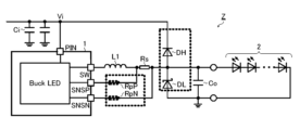
- surge protection diodes DH and DL are externally attached to the LED driver IC1 as a means for protecting the electrostatic protection diode Desd (see FIG. 5) mentioned above from surge current. ing.
- the surge protection diode DH is connected between the anode of the LED string 2 and the end to which the input voltage Vi is applied. Further, the surge protection diode DL is connected between the anode of the LED string 2 and the ground terminal.
- the anode potential of the LED string 2 can be clamped within a predetermined range, so that the electrostatic protection diode Desd of the LED driver IC1 can be It becomes possible to protect.
- the current limiting resistor RpP is preferably connected between the SNSP pin and the first end (high potential end) of the sense resistor Rs.
- the current limiting resistor RpN is preferably connected between the SNSN pin and the second end (low potential end) of the sense resistor Rs.
- FIG. 8 is a diagram showing how a gain error occurs in the current sense amplifier 16 due to the external connection of the current limiting resistors RpP and RpN.
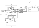
- the current sense amplifier 16 includes a current output type differential amplifier AMP1, input resistors R1P and R1N, and an output resistor R2.
- a non-inverting input terminal (+) of the differential amplifier AMP1 is connected to a first terminal of an input resistor R1P (for example, 10 k ⁇ ).
- a second end of input resistor R1P is connected to the SNSP pin.
- An inverting input terminal (-) of the differential amplifier AMP1 is connected to a first terminal of an input resistor R1N (for example, 10 k ⁇ ).
- a second end of the input resistor R1N is connected to the SNSN pin.
- the output terminal of the differential amplifier AMP1 is connected to the first terminal of the output resistor R2 (for example, 120 k ⁇ ), and is also connected to the non-inverting input terminal (+) of the differential amplifier AMP1.
- a second end of the output resistor R2 is connected to a ground terminal.
- the slope signal generation section 15 includes a current output type differential amplifier AMP2, input resistors R3P and R3N, and an output resistor R4.
- a non-inverting input terminal (+) of the differential amplifier AMP2 is connected to a first terminal of an input resistor R3P (for example, 10 k ⁇ ).
- a second end of input resistor R3P is connected to the SNSP pin.
- the inverting input terminal (-) of the differential amplifier AMP2 is connected to the first terminal of the input resistor R3N (for example, 10 k ⁇ ).
- a second end of input resistor R3N is connected to the SNSN pin.
- the output terminal of the differential amplifier AMP2 is connected to the first terminal of the output resistor R4 (for example, 10 k ⁇ ), and is also connected to the non-inverting input terminal (+) of the differential amplifier AMP2.
- a second end of the output resistor R4 is connected to a ground terminal.
- a feedback current I1 flows between the non-inverting input terminal (+) and the output terminal of the differential amplifier AMP1.
- This feedback current I1 is essential for performing highly accurate current feedback control.
- a feedback current I2 flows between the non-inverting input terminal (+) and the output terminal of the differential amplifier AMP2.
- the general current sense amplifier 16 for performing nonlinear control of the average inductor current IL_ave has a floating input stage that can amplify the sense voltage Vsns rail-to-rail (between the power supply potential and the ground potential).
- AMP1 includes a differential amplifier AMP1.
- "floating" means floating from the ground potential (separated from the ground potential).
- the feedback currents I1 and I2 become larger, the fluctuations in the current detection signal VISET also become larger.
- the input resistor R1 and output resistor R2 built into the LED driver IC1 are paired with each other, they work to cancel their respective temperature characteristics, but the external current limiting resistors RpP and RpN In addition to having completely different temperature coefficients from the input resistance R1 and the output resistance R2, there are also manufacturing variations in each. Therefore, the temperature characteristics of the final current detection signal VISET vary greatly.
- FIG. 9 is a diagram showing a fourth embodiment of the LED lamp module.
- the aforementioned components LED driver IC1, LED string 2, inductor L1, capacitor Co, sense resistor Rs, and current limiting resistors RpP and RpN
- the MCU 4 is configured to control both channels in an integrated manner.
- the LED driver ICs 1A and 1B each have a buck converter that supplies power to the LED strings 2A and 2B, a temperature detection unit that detects the internal junction temperature Tj, and SPI [serial peripheral interface] communication with the MCU 4. It is equipped with a communications department and other facilities.
- a problem caused by externally attaching the current limiting resistors RpPA and RpNA and the current limiting resistors RpPB and RpNB is a decrease in current detection accuracy (particularly temperature drift) in each of the LED driver ICs 1A and 1B.
- a solution to this problem is, for example, a method of monitoring the internal junction temperature Tj of each of the LED driver ICs 1A and 1B using the MCU 4, and dynamically constantly correcting the detection results of the sense voltages VsnsA and VsnsB based on the monitoring results. is possible.
- FIG. 10 is a diagram showing the temperature characteristics of the detection result of the sense voltage Vsns (corresponding to the aforementioned current detection signal VISET).
- the thick solid line VsnsA indicates the detection result of the sense voltage VsnsA in the LED driver IC1A.
- a thick solid line VsnsB indicates the detection result of the sense voltage VsnsB in the LED driver IC1B.
- a thick broken line Vsns (typ.) indicates a temperature characteristic that is a correction reference in the MCU 4.
- FIG. 11 is a diagram showing a fifth embodiment of the LED lamp module.
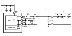
- the LED driver IC1 has a functional unit ( ⁇ IBIASctl) for reducing the differential input current difference ⁇ IBIAS of the differential amplifier AMP1 (see FIG. 8) forming the current sense amplifier 16. Even if the current limiting resistors RpP and RpN are externally attached, the gain error of the current sense amplifier 16 is reduced.
- FIG. 12 is a diagram showing the elimination of gain errors in the current sense amplifier 16.
- the current sense amplifier 16 is configured to flow a feedback current I1 between the non-inverting input terminal (+) and the output terminal of the differential amplifier AMP1.
- the second feedback current path is configured to flow a feedback current I1' between the SNSN pin and the output terminal of the differential amplifier AMP1.
- the feedback current I1' is a copy (mirror current) of the feedback current I1, and the respective current values may be set to the same value (maximum about 20 ⁇ A). In this way, by flowing the feedback current I1' having the same value as the feedback current I1 also on the reference side of the differential amplifier AMP1, the differential input current difference ⁇ IBIAS can be brought close to zero.
- the feedback current I1 and the feedback current I1' have exactly the same value, and for example, an arbitrary offset may be provided between them.
- the slope signal generation unit 15 includes a gm amplifier AMP2g that detects the sense voltage Vsns appearing between the SNSP pin and the SNSN pin without drawing current from the SNSP and SNSN pins, instead of the differential amplifier AMP2 mentioned above.
- the aforementioned feedback current I2 can be made zero by using the gm amplifier AMP2g that does not require feedback current control.
- the gain G of the current sense amplifier 16 is adjusted according to the ratio of the input resistor R1 and the output resistor R2. Since it is uniquely determined, it is possible to eliminate a decrease in current detection accuracy (especially temperature drift) in the LED driver IC1.
- the electrostatic protection diode Desd (see FIG. 5) of the LED driver IC1 can be protected from surge currents ID1 and ID2. Therefore, two external surge protection diodes DH and DL, which were required for each channel, are no longer required. As a result, it is possible to reduce the cost of the LED lamp module Z and to reduce the component mounting area on the board.
- the on-time setting unit 14 uses a source follower that detects the terminal voltage appearing at the SNSN pin without drawing current from the SNSP and SNSN pins, instead of the resistor voltage divider circuit described above. It is desirable to use
- FIG. 13 is a diagram showing a sixth embodiment of the LED lamp module.
- the LED driver IC 1 includes a valley current control section 20, a current sense amplifier 21, a VI converter 22, and a DAC 23 in place of the components 15 to 19 in FIG. has.
- input resistors R5P and R5N for example, both 10 k ⁇
- feedback resistors R6P and R6N for example, both 140 k ⁇
- These components 20 to 23 can all be understood as components of a current detection circuit.
- the valley current control unit 20 detects the bottom (valley detection) of the inductor current IL based on the sense voltage Vsns generated across the sense resistor Rs and the current detection signal CS generated by the current sense amplifier 21. By doing so, the previously mentioned set signal SET is generated.
- the current sense amplifier 21 is a current output type differential amplifier equipped with a floating input stage that can amplify an input signal rail-to-rail.
- the inverting input terminal (-) of the current sense amplifier 21 is connected to the first terminal of the input resistor R5P.
- the second end of input resistor R5P is connected to the SNSP pin.
- a non-inverting input terminal (+) of the current sense amplifier 21 is connected to a first terminal of the input resistor R5N.
- the second end of input resistor R5N is connected to the SNSN pin.
- the output end of the current sense amplifier 21 is connected to a phase compensation capacitor Cc via a COMP pin.
- the drain of the NMOSFET 22b is connected to the inverting input terminal (-) of the current sense amplifier 21 and the first terminal of the input resistor R5P.
- the source of the NMOSFET 22b is connected to the first end of the feedback resistor R6P and the inverting input end (-) of the operational amplifier 22a.
- a second end of the feedback resistor R6P is connected to a ground terminal.
- the gate of NMOSFET 22b is connected to the output terminal of operational amplifier 22a.
- the DAC 23 converts a digital signal (for example, 10 bits) (not shown) into an analog current adjustment voltage VIadj.
- a current detection signal CS is generated.
- This current detection signal CS controls the bottom detection value (valley detection value) of the inductor current IL.
- the output current ILED is adjusted to VIadj ⁇ R5P/(R6P ⁇ Rs).
- FIG. 14 is a diagram equivalently showing the current detection circuit of the sixth embodiment. Note that the feedback resistor R6 in this figure may be understood as the feedback resistor R6P (or feedback resistor R6N) in FIG. 13.
- the reference currents I11 and I11' may have the same value, or may have an arbitrary offset between them.
- the current limiting resistors RpP and RpN are externally connected to the SNSP pin and the SNSN pin, respectively. Even if the gain of the VI converter 22 (and by extension the reference voltage of the current sense amplifier 21) is uniquely determined according to the ratio of the input resistor R5P and the feedback resistor R6, the current detection in the LED driver IC1 is It becomes possible to eliminate a decrease in accuracy (especially temperature drift).
- FIG. 15 is a diagram showing a seventh embodiment of the LED lamp module (corresponding to a first comparative example to be compared with the eighth and ninth embodiments described later).
- the LED driver IC 1 is based on the first embodiment (FIG. 1) described above, but includes a current sense amplifier 31 and an error amplifier in place of the components 15 to 17 and 19. 32 and a VI converter 33.
- the current sense amplifier 31 is a functional block that generates a slope signal Vslp including current information regarding the inductor current IL according to the sense voltage Vsns_IC applied between the SNSP pin and the SNSN pin, and outputs it to the comparator 18 (not shown). , a gm amplifier AMP31, input resistors R7P and R7N, and an output resistor R8.
- the gm amplifier AMP31 also has a first feedback current path configured to flow a first feedback current i11 between its output end and a non-inverting input end (+), and a first feedback current path configured to flow a first feedback current i11 between its output end and a non-inverting input end (- ) and a second feedback current path configured to flow a second feedback current i11' between the two.
- the second feedback current i11' may be a copy (mirror current) of the first feedback current i11, or may be a copy of the first feedback current i11 given an offset.
- the error amplifier 32 is a functional block that generates an error signal Vc according to the sense voltage Vsns_IC applied between the SNSP pin and the SNSN pin, and includes a gm amplifier AMP32, input resistors R9P and R9N, and a capacitor Cc. .
- the non-inverting input terminal (+) of the gm amplifier AMP32 is connected to the first terminal of the input resistor R9P.
- the second end of the input resistor R9P is connected to the power supply end of the gm amplifier AMP32 and the SNSP pin.
- the inverting input terminal (-) of the gm amplifier AMP32 is connected to the first terminal of the input resistor R9N.
- a second end of input resistor R9N is connected to the SNSN pin.
- the output end of the gm amplifier AMP32 is connected to the first end of the capacitor Cc.
- a second end of the capacitor Cc is connected to a ground end.
- the VI converter 33 is a functional block that converts the current adjustment voltage VIadj into a reference current i12, and includes a gm amplifier AMP33 and a feedback resistor R10.
- the current sense amplifier 31 for detecting the current ripple component ⁇ IL and the error amplifier 32 for detecting the average inductor current IL_ave are connected in parallel to the SNSP pin and the SNSN pin. It is connected.
- the difference between the sense voltage Vsns_IC and the reference voltage becomes 0 due to output feedback control.
- FIG. 16 is a diagram showing an eighth embodiment of the LED lamp module.
- the LED driver IC 1 is based on the above-mentioned first embodiment (FIG. 1), but includes a current sense amplifier 41 and an error amplifier in place of the components 15 to 17 and 19. 42 and a VI converter 43.
- the current sense amplifier 41 is a functional block that generates a current detection signal Vcso including current information regarding the inductor current IL according to the sense voltage Vsns_IC applied between the SNSP pin and the SNSN pin, and outputs it to the comparator 18 (not shown). It includes a gm amplifier AMP41, input resistors R11P and R11N, and an output resistor R12.
- the non-inverting input terminal (+) of the gm amplifier AMP41 is connected to the first terminal of the input resistor R11P.
- the second end of the input resistor R11P is connected to the SNSP pin.
- the inverting input terminal (-) of the gm amplifier AMP41 is connected to the first terminal of the input resistor R11N.
- the second end of the input resistor R11N is connected to the SNSN pin.
- the output end of the gm amplifier AMP41 is connected to the first end of the output resistor R12.
- the second end of the output resistor R12 is connected to the application end of the reference signal Vref.
- the gm amplifier AMP41 has a first feedback current path configured to flow a first feedback current i21 between its output end and a non-inverting input end (+), and a first feedback current path configured to flow a first feedback current i21 between its output end and a non-inverting input end (- ) and a second feedback current path configured to flow a second feedback current i21' between the two.
- the second feedback current i21' may be a copy (mirror current) of the first feedback current i21, or may be a copy of the first feedback current i21 given an offset.
- the error amplifier 42 is a functional block that generates an error signal Vc according to the error between the current detection signal Vcso and a predetermined reference signal Vref, and includes a gm amplifier AMP42 and a capacitor Cc.
- the non-inverting input terminal (+) of the gm amplifier AMP42 is connected to the application terminal of the reference signal Vref.
- the inverting input terminal (-) of the gm amplifier AMP42 is connected to the application terminal of the current detection signal Vcso.
- the output end of the gm amplifier AMP42 is connected to the first end of the capacitor Cc. A second end of the capacitor Cc is connected to a ground end.
- the VI converter 43 is a functional block that converts the current adjustment voltage VIadj into a reference current i22, and includes a gm amplifier AMP43 and a feedback resistor R13.
- the current sense amplifier 41 and the error amplifier 42 have a common input system.
- the current sense amplifier 41 and the error amplifier 42 are connected in series to the SNSP pin and the SNSN pin.
- FIG. 17 is a diagram showing a ninth embodiment of the LED lamp module.
- the LED driver IC 1 is based on the previous eighth embodiment (FIG. 16), but has additional features to bring the current difference between the SNSP pin and the SNSN pin close to 0. It's elaborate.
- the VI converter 43 causes the aforementioned reference current i22 to flow through the input resistor R11P, and draws in a correction current i22' equal to the reference current i22 directly from the SNSN pin. This point is as shown in FIG. 13 mentioned earlier.
- the electrostatic protection diode Desd (see FIG. 5) of the LED driver IC1 can be protected from surge currents ID1 and ID2. Therefore, two external surge protection diodes DH and DL, which were required for each channel, are no longer required. As a result, it is possible to reduce the cost of the LED lamp module Z and to reduce the component mounting area on the board.
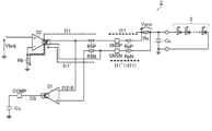
- FIG. 18 is a diagram showing a tenth embodiment of the LED lamp module (corresponding to a second comparative example compared to the eleventh embodiment described later). This figure depicts an example of a more specific circuit configuration based on the first embodiment (FIG. 1) described above. Therefore, the constituent elements that have already appeared will be given the same reference numerals as those in FIG. 1, redundant explanations will be omitted, and new constituent elements and changes will be mainly explained.
- the LED driver IC1 of this embodiment includes resistors R21, R22, and Ro are integrated.
- the LED driver IC1 of this embodiment there is a connection between the first end (high potential end) of the sense resistor Rs and the SNSP pin, and between the second end (low potential end) of the sense resistor Rs and the SNSN pin. , are connected to current limiting resistors RpP and RpN, respectively.
- the error signal Vc is generated by outputting a current according to the voltage and charging and discharging the capacitor Cc. Therefore, the error signal Vc rises when VISET ⁇ Vdcdim, and falls when VISET>Vdcdim.
- a resistor ro is connected in parallel with the capacitor Cc between the output terminal of the error amplifier 17 and the ground terminal. Note that the capacitor Cc is for phase compensation. Further, the resistor ro is the output impedance of the error amplifier 17, and does not exist as an actual element.
- the slope signal generation section 15 is a gm amplifier that operates by receiving current from the PIN pin and can detect the sense voltage Vsns appearing between both terminals without drawing current from the SNSP and SNSN pins. Note that a resistor R22 is connected between the output end of the slope signal generation section 15 and the ground end.
- the current sense amplifier 16 operates by receiving power from the PIN pin, amplifies the sense voltage Vsns, and generates the current detection signal VISET.
- a non-inverting input terminal (+) of the current sense amplifier 16 is connected to the SNSP pin via an input resistor R1P.
- the inverting input terminal (-) of the current sense amplifier 16 is connected to the SNSN pin via an input resistor R1N.
- a second end of the resistor R21 is connected to a ground terminal.
- the current sense amplifier 16 has a first feedback current path configured to flow the first feedback current i31 between its output terminal and the non-inverting input terminal (+), and between the output terminal and the SNSN pin. and a second feedback current path configured to flow a second feedback current i31'.
- the second feedback current i31' may be a copy (mirror current) of the first feedback current i31, or may be a copy of the first feedback current i31 given an offset.
- the electrostatic protection diode Desd (FIG. 5) built in each of the SNSP pin and the SNSN pin can be protected from surge current. Therefore, the external surge protection diodes DH and DL (FIG. 7) are not required, so it is possible to reduce the cost of the LED lamp module Z and to reduce the component mounting area on the board.
- the symbol Gcs indicates the gain of the slope signal generation section 15.
- the symbol Gsns indicates the gain of the current sense amplifier 16.
- the symbol ⁇ Vsns indicates the sense voltage Vsns.
- the symbol X indicates a current setting value (target value) of the output current ILED.
- the symbol ⁇ Vc indicates the error signal Vc.
- ⁇ D indicates the off-duty of the lower switch 11L (control of the bottom value of the inductor current IL ⁇ control of the off period).
- the symbol Cc indicates the capacitance value of the capacitor Cc.
- FIG. 20 is a diagram showing an eleventh embodiment of the LED lamp module.
- the LED driver IC 1 of this embodiment includes a bias amplifier 1A and a VI A converter 1B, transistors P1a and P1b (for example, PMOSFET [P-channel type MOSFET]), and resistors R31a, R31b, R32a, R32b, R33, R34a, R34b, and Ro are integrated.
- the previously mentioned slope signal generation section 15 is removed.
- the LED driver IC1 of this embodiment there is a connection between the first end (high potential end) of the sense resistor Rs and the SNSP pin, and between the second end (low potential end) of the sense resistor Rs and the SNSN pin. , are connected to current limiting resistors RpP and RpN, respectively. This point is similar to FIG. 18 mentioned earlier.
- the LED driver IC1 of this embodiment includes a second reference current path configured to flow a second reference current i41' between the SNSN pin and the second output terminal of the VI converter 1B.
- the first reference current i41 and the second reference current i41' may have the same value, or an arbitrary offset may be provided between them.
- the current limiting resistor RpP and the current limiting resistor RpP are connected to the SNSP pin and the SNSN pin respectively. Even if RpN is externally connected, the gain of the VI converter 1B (and by extension the reference voltage of the current sense amplifier 16) is uniquely determined according to the ratio of the input resistor R1P and the resistor R33, so the LED driver IC1 It becomes possible to eliminate the decrease in current detection accuracy (particularly temperature drift).
- the second differential output terminal of the current sense amplifier 16 is connected to the first terminal of the resistor R31b, and is also connected to the non-inverting input terminal (+) of the error amplifier 17.
- the second ends of the resistors R31a and R31b are both connected to a ground terminal.
- resistors R32a and R32b are connected in series between the non-inverting input terminal (+) and the inverting input terminal (-) of the current sense amplifier 16, and the current sense amplifier 16 is driven from the connection node between them. Voltage is supplied.
- the error amplifier 17 outputs a current according to the current detection signal ⁇ Vcso that is differentially input between the non-inverting input terminal (+) and the inverting input terminal (-), and charges and discharges the capacitor Cc to eliminate the error. Generates signal Vc. Note that a resistor Ro is connected in parallel with the capacitor Cc between the output terminal of the error amplifier 17 and the ground terminal.
- the gate of the transistor P1a is connected to the first differential output terminal of the current sense amplifier 16.
- the drain of transistor P1a is connected to a ground terminal.
- the source of transistor P1a is connected to the first end of resistor R34a.
- the second end of the resistor R34a is connected to the inverting input end (-) of the comparator 18.
- the transistor P1a connected in this manner functions as a first voltage follower (first source follower) connected between the first differential output terminal of the current sense amplifier 16 and the inverting input terminal (-) of the comparator 18. do.
- the gate of the transistor P1b is connected to the second differential output terminal of the current sense amplifier 16.
- the drain of transistor P1b is connected to the ground terminal.
- the source of transistor P1b is connected to the first end of resistor R34b.
- the second end of the resistor R34b is connected to the non-inverting input end (+) of the comparator 18.
- the transistor P1b connected in this manner functions as a second voltage follower (second source follower) connected between the second differential output terminal of the current sense amplifier 16 and the non-inverting input terminal (+) of the comparator 18. Function.
- the bias amplifier 1A applies a differential signal to each of the resistors R34a and R34b according to the difference between the error signal Vc input to the non-inverting input terminal (+) and the bias voltage Vbias input to the inverting input terminal (-). By outputting current, the respective operating points of the first voltage follower and the second voltage follower are determined.
- the logic level of the set signal SET is switched when (VcsoP-Vc)-(VcsoN+Vc)>0, that is, when ⁇ Vcso-2Vc>0.
- the bottom value of the inductor current IL is detected at the point where the current information ⁇ Vcso reaches the control voltage Vc.
- the differential input difference of the current sense amplifier 16 will be 0 (DC error is 0), so the current difference between the SNSP pin and the SNSN pin will be Does not occur.
- the slope signal generation section 15 can be integrated into the current sense amplifier 16 to reduce the circuit scale.
- the symbol Gsns indicates the gain of the current sense amplifier 16.
- the symbol ⁇ Vsns indicates the sense voltage Vsns.
- the symbol X indicates a current setting value (target value) of the output current ILED.
- the symbol ⁇ Vc indicates the error signal Vc.
- ⁇ D indicates the off-duty of the lower switch 11L (control of the bottom value of the inductor current IL ⁇ control of the off period).
- the symbol Cc indicates the capacitance value of the capacitor Cc.
- the semiconductor device disclosed herein includes a current detection circuit configured to generate a current detection signal according to a current to be monitored, and a current detection circuit configured to generate a current detection signal according to an error between the current detection signal and a predetermined reference signal.
- an error amplifier configured to generate an error signal;
- a comparator configured to compare the error signal and the current detection signal to generate a set signal; and
- a comparator configured to receive input of the set signal and monitor the set signal.
- a controller configured to control a target current
- the current detection circuit includes a current output type differential amplifier, and a current detection circuit between a first input terminal of the differential amplifier and a first current sense terminal.
- a first input resistor configured to be connected to the differential amplifier; a second input resistor configured to be connected between the second input terminal of the differential amplifier and a second current sense terminal; an output resistor configured to be connected to an output terminal of the amplifier; and a first feedback current configured to flow a first feedback current between the first input terminal and the output terminal of the differential amplifier. and a second feedback current path configured to flow a second feedback current between the second input terminal and the output terminal of the differential amplifier (first configuration).
- the first feedback current and the second feedback current may have the same value (second configuration).
- the semiconductor device according to the first configuration may have a configuration (third configuration) in which an offset is provided to the first feedback current and the second feedback current.
- the semiconductor device disclosed in this specification includes a current detection circuit configured to generate a current detection signal according to a current to be monitored, and an error between the current detection signal and a predetermined reference signal.
- an error amplifier configured to generate a corresponding error signal;
- a comparator configured to generate a set signal by comparing the error signal and the current detection signal; and
- a comparator configured to receive the input of the set signal.
- a controller configured to control the current to be monitored;
- the current detection circuit includes a current output type differential amplifier; and a connection between a first input terminal of the differential amplifier and a first current sense terminal.
- a first input resistor configured to be connected between a second input resistor configured to be connected between a second input terminal of the differential amplifier and a second current sense terminal; a VI converter configured to convert a signal into a current signal; a feedback resistor configured to determine a gain of the VI converter; and a first current sense terminal and a first current sense terminal of the VI converter.
- a first reference current path configured to flow a first reference current between the second current sense terminal and the second output terminal of the VI converter; and a second reference current path configured to flow the current (fourth configuration).
- the semiconductor device includes an on-time setting section configured to generate a pulse in the reset signal when a predetermined on-time has elapsed from the pulse generation timing of the set signal.
- the controller further includes a configuration (fifth configuration) in which the controller controls the monitored current to match a predetermined target value using a bottom detection on-time fixed method according to the set signal and the reset signal. good.
- the on-time setting section detects a terminal voltage appearing at the second current sense terminal without drawing current from the first current sense terminal and the second current sense terminal.
- a configuration (sixth configuration) including a source follower configured to do this may also be used.
- a module disclosed in this specification includes a semiconductor device having any one of the first to sixth configurations, an inductor, a sense resistor, and a load connected in series to an output element, and the first current sense terminal. and a second current limiting resistor connected between the second current sense terminal and the sense resistor (seventh configuration). It is said that
- the load may include a light emitting diode element (eighth configuration).
- the module according to the eighth configuration may further include a matrix manager configured to arbitrarily switch the number of series stages of the light emitting diode elements (ninth configuration).
Landscapes
- Engineering & Computer Science (AREA)
- Power Engineering (AREA)
- Circuit Arrangement For Electric Light Sources In General (AREA)
- Measurement Of Current Or Voltage (AREA)
Priority Applications (4)
| Application Number | Priority Date | Filing Date | Title |
|---|---|---|---|
| DE112023000986.4T DE112023000986B4 (de) | 2022-03-31 | 2023-02-17 | Halbleiterbauteil und modul |
| JP2024511416A JPWO2023188965A1 (https=) | 2022-03-31 | 2023-02-17 | |
| CN202380031202.XA CN118975112A (zh) | 2022-03-31 | 2023-02-17 | 半导体装置、模块 |
| US18/895,104 US20250016896A1 (en) | 2022-03-31 | 2024-09-24 | Semiconductor device and module |
Applications Claiming Priority (2)
| Application Number | Priority Date | Filing Date | Title |
|---|---|---|---|
| JP2022060375 | 2022-03-31 | ||
| JP2022-060375 | 2022-03-31 |
Related Child Applications (1)
| Application Number | Title | Priority Date | Filing Date |
|---|---|---|---|
| US18/895,104 Continuation US20250016896A1 (en) | 2022-03-31 | 2024-09-24 | Semiconductor device and module |
Publications (1)
| Publication Number | Publication Date |
|---|---|
| WO2023188965A1 true WO2023188965A1 (ja) | 2023-10-05 |
Family
ID=88200353
Family Applications (1)
| Application Number | Title | Priority Date | Filing Date |
|---|---|---|---|
| PCT/JP2023/005650 Ceased WO2023188965A1 (ja) | 2022-03-31 | 2023-02-17 | 半導体装置、モジュール |
Country Status (5)
| Country | Link |
|---|---|
| US (1) | US20250016896A1 (https=) |
| JP (1) | JPWO2023188965A1 (https=) |
| CN (1) | CN118975112A (https=) |
| DE (1) | DE112023000986B4 (https=) |
| WO (1) | WO2023188965A1 (https=) |
Cited By (1)
| Publication number | Priority date | Publication date | Assignee | Title |
|---|---|---|---|---|
| US20250016896A1 (en) * | 2022-03-31 | 2025-01-09 | Rohm Co., Ltd. | Semiconductor device and module |
Families Citing this family (1)
| Publication number | Priority date | Publication date | Assignee | Title |
|---|---|---|---|---|
| JP2025018051A (ja) * | 2023-07-26 | 2025-02-06 | セイコーエプソン株式会社 | 半導体回路装置及びスイッチングレギュレーター |
Citations (5)
| Publication number | Priority date | Publication date | Assignee | Title |
|---|---|---|---|---|
| JP2006262265A (ja) * | 2005-03-18 | 2006-09-28 | Rohm Co Ltd | 演算増幅器およびそれを用いた増幅回路、ならびに電子機器 |
| JP2010110148A (ja) * | 2008-10-31 | 2010-05-13 | Panasonic Corp | 電源装置 |
| JP2017175415A (ja) * | 2016-03-24 | 2017-09-28 | ヤマハ株式会社 | 電流検出装置 |
| JP2021044283A (ja) * | 2019-09-06 | 2021-03-18 | ローム株式会社 | 発光素子駆動装置 |
| JP2022056872A (ja) * | 2020-09-30 | 2022-04-11 | ローム株式会社 | 電流検出回路 |
Family Cites Families (12)
| Publication number | Priority date | Publication date | Assignee | Title |
|---|---|---|---|---|
| WO2013077269A1 (ja) * | 2011-11-21 | 2013-05-30 | パナソニック株式会社 | 電源装置、点灯装置、灯具、及び車両 |
| US8896214B2 (en) * | 2011-12-19 | 2014-11-25 | Monolithic Power Systems, Inc. | LED driving system for driving multi-string LEDs and the method thereof |
| US9585207B2 (en) * | 2014-07-11 | 2017-02-28 | General Electric Company | System and method for achieving precise regulation of multiple outputs in a multi-resonant LED driver stage |
| CN104270861B (zh) * | 2014-09-30 | 2017-01-18 | 成都芯源系统有限公司 | Led驱动器、控制电路及led驱动方法 |
| EP3624566B1 (en) | 2015-08-04 | 2021-04-07 | Koito Manufacturing Co., Ltd. | Lighting circuit |
| US11193957B2 (en) * | 2019-08-13 | 2021-12-07 | Analog Devices International Unlimited Company | Shunt resistor averaging techniques |
| EP4298866A1 (en) * | 2021-02-23 | 2024-01-03 | Signify Holding B.V. | Multi-channel driver with switchable by pass capacitors |
| JPWO2023188964A1 (https=) * | 2022-03-31 | 2023-10-05 | ||
| CN118975112A (zh) * | 2022-03-31 | 2024-11-15 | 罗姆股份有限公司 | 半导体装置、模块 |
| US11990175B2 (en) * | 2022-04-01 | 2024-05-21 | Micron Technology, Inc. | Apparatuses and methods for controlling word line discharge |
| US12395063B1 (en) * | 2022-08-18 | 2025-08-19 | Zhonghui BING | Control system for a bi-directional totem-pole ac-dc converter |
| TWI890420B (zh) * | 2024-04-29 | 2025-07-11 | 茂達電子股份有限公司 | 隨電流動態調整電壓餘裕的電源轉換器 |
-
2023
- 2023-02-17 CN CN202380031202.XA patent/CN118975112A/zh active Pending
- 2023-02-17 DE DE112023000986.4T patent/DE112023000986B4/de active Active
- 2023-02-17 JP JP2024511416A patent/JPWO2023188965A1/ja active Pending
- 2023-02-17 WO PCT/JP2023/005650 patent/WO2023188965A1/ja not_active Ceased
-
2024
- 2024-09-24 US US18/895,104 patent/US20250016896A1/en active Pending
Patent Citations (5)
| Publication number | Priority date | Publication date | Assignee | Title |
|---|---|---|---|---|
| JP2006262265A (ja) * | 2005-03-18 | 2006-09-28 | Rohm Co Ltd | 演算増幅器およびそれを用いた増幅回路、ならびに電子機器 |
| JP2010110148A (ja) * | 2008-10-31 | 2010-05-13 | Panasonic Corp | 電源装置 |
| JP2017175415A (ja) * | 2016-03-24 | 2017-09-28 | ヤマハ株式会社 | 電流検出装置 |
| JP2021044283A (ja) * | 2019-09-06 | 2021-03-18 | ローム株式会社 | 発光素子駆動装置 |
| JP2022056872A (ja) * | 2020-09-30 | 2022-04-11 | ローム株式会社 | 電流検出回路 |
Cited By (1)
| Publication number | Priority date | Publication date | Assignee | Title |
|---|---|---|---|---|
| US20250016896A1 (en) * | 2022-03-31 | 2025-01-09 | Rohm Co., Ltd. | Semiconductor device and module |
Also Published As
| Publication number | Publication date |
|---|---|
| DE112023000986T5 (de) | 2024-12-05 |
| JPWO2023188965A1 (https=) | 2023-10-05 |
| CN118975112A (zh) | 2024-11-15 |
| DE112023000986B4 (de) | 2025-07-17 |
| US20250016896A1 (en) | 2025-01-09 |
Similar Documents
| Publication | Publication Date | Title |
|---|---|---|
| US12016095B2 (en) | Systems and methods for regulating LED currents | |
| JP7520668B2 (ja) | 電流検出回路 | |
| CN107656124B (zh) | 无需外部采样电阻的Boost负载电流检测电路及方法 | |
| JP4778226B2 (ja) | Dc−dcコンバータ | |
| US8344656B2 (en) | Methods and systems for LED driver having constant output current | |
| CN111596715B (zh) | 电压调整装置、芯片、电源及电子设备 | |
| US20250016896A1 (en) | Semiconductor device and module | |
| US11265981B2 (en) | Light emitting element driving device | |
| US20080007322A1 (en) | Power supply apparatus | |
| EP4134778A1 (en) | Voltage regulating apparatus, chip, power supply, and electronic device | |
| US8742743B2 (en) | Switching control circuit | |
| US20250024568A1 (en) | Light-emitting element drive device, light emission control device, and light emission device | |
| US11057976B2 (en) | Short to ground and open protecting circuit, and associated protecting method | |
| US9531259B2 (en) | Power supply circuit | |
| CN108075655B (zh) | 电源转换装置 | |
| CN112351551A (zh) | 调光电路 | |
| JP2024053910A (ja) | 降圧dc/dcコンバータのコントローラ回路、車載電源システム | |
| US12557192B2 (en) | Semiconductor device, switching power supply, and lighting device | |
| CN211857324U (zh) | 电压调整装置、芯片、电源及电子设备 | |
| US7795755B2 (en) | Simple circuit and method for improving current balance accuracy of a power converter system | |
| JP2019103289A (ja) | 電源装置及びこれを備えた光照射システム | |
| CN101772235A (zh) | 具有温度补偿的发光二极管驱动电路及其控制器 | |
| JP2024083794A (ja) | 電源制御装置 |
Legal Events
| Date | Code | Title | Description |
|---|---|---|---|
| 121 | Ep: the epo has been informed by wipo that ep was designated in this application |
Ref document number: 23778995 Country of ref document: EP Kind code of ref document: A1 |
|
| ENP | Entry into the national phase |
Ref document number: 2024511416 Country of ref document: JP Kind code of ref document: A |
|
| WWE | Wipo information: entry into national phase |
Ref document number: 202380031202.X Country of ref document: CN |
|
| WWE | Wipo information: entry into national phase |
Ref document number: 112023000986 Country of ref document: DE |
|
| 122 | Ep: pct application non-entry in european phase |
Ref document number: 23778995 Country of ref document: EP Kind code of ref document: A1 |
|
| WWG | Wipo information: grant in national office |
Ref document number: 112023000986 Country of ref document: DE |