WO2023182303A1 - モータ駆動装置 - Google Patents
モータ駆動装置 Download PDFInfo
- Publication number
- WO2023182303A1 WO2023182303A1 PCT/JP2023/010992 JP2023010992W WO2023182303A1 WO 2023182303 A1 WO2023182303 A1 WO 2023182303A1 JP 2023010992 W JP2023010992 W JP 2023010992W WO 2023182303 A1 WO2023182303 A1 WO 2023182303A1
- Authority
- WO
- WIPO (PCT)
- Prior art keywords
- signal
- circuit
- current
- pulse
- switch element
- Prior art date
- Legal status (The legal status is an assumption and is not a legal conclusion. Google has not performed a legal analysis and makes no representation as to the accuracy of the status listed.)
- Ceased
Links
Images


Classifications
-
- H—ELECTRICITY
- H02—GENERATION; CONVERSION OR DISTRIBUTION OF ELECTRIC POWER
- H02P—CONTROL OR REGULATION OF ELECTRIC MOTORS, ELECTRIC GENERATORS OR DYNAMO-ELECTRIC CONVERTERS; CONTROLLING TRANSFORMERS, REACTORS OR CHOKE COILS
- H02P23/00—Arrangements or methods for the control of AC motors characterised by a control method other than vector control
- H02P23/14—Estimation or adaptation of motor parameters, e.g. rotor time constant, flux, speed, current or voltage
-
- H—ELECTRICITY
- H02—GENERATION; CONVERSION OR DISTRIBUTION OF ELECTRIC POWER
- H02P—CONTROL OR REGULATION OF ELECTRIC MOTORS, ELECTRIC GENERATORS OR DYNAMO-ELECTRIC CONVERTERS; CONTROLLING TRANSFORMERS, REACTORS OR CHOKE COILS
- H02P27/00—Arrangements or methods for the control of AC motors characterised by the kind of supply voltage
- H02P27/04—Arrangements or methods for the control of AC motors characterised by the kind of supply voltage using variable-frequency supply voltage, e.g. inverter or converter supply voltage
- H02P27/06—Arrangements or methods for the control of AC motors characterised by the kind of supply voltage using variable-frequency supply voltage, e.g. inverter or converter supply voltage using DC to AC converters or inverters
- H02P27/08—Arrangements or methods for the control of AC motors characterised by the kind of supply voltage using variable-frequency supply voltage, e.g. inverter or converter supply voltage using DC to AC converters or inverters with pulse width modulation
Definitions
- the present disclosure relates to a motor drive device.
- Motor drive devices that drive a motor with low noise and low vibration include one disclosed in Patent Document 1, for example.
- the motor drive device disclosed in Patent Document 1 uses a resistor to detect the current flowing through the motor coil due to the switching operation of a switch element, and applies PWM (Pulse Width Modulation) to the current so that the peak value of the detected voltage follows a reference voltage.
- PWM Pulse Width Modulation
- the aim is to achieve low noise and vibration through pulse width modulation (pulse width modulation) control.
- the reference voltage is a voltage that sets a target value of the current flowing through the motor coil.
- Patent Document 1 also discloses a countermeasure by switching the switching operation mode near the zero-crossing point.
- the setting of the minimum on-period differs depending on the characteristics of the switch element, and the minimum on-period is set to be long with some margin due to the versatility of the switch element drive circuit, so the current waveform deviates from the target waveform near the zero-crossing point. The problem becomes obvious.
- the present disclosure solves these problems and provides a motor drive device that can cause a current waveform near a zero-crossing point to accurately follow a target waveform.
- a motor drive device that drives a motor, and includes a first series switch circuit including a first high side switch element and a first low side switch element, and a first series switch circuit including a first high side switch element and a first low side switch element.
- a second series switch circuit including a second high-side switch element and a second low-side switch element and connected in parallel to the first series switch circuit, and a reference pulse signal having a pulse duration greater than zero; a reference pulse generation circuit that generates a reference pulse with a period of , a current detection unit that outputs a current signal corresponding to a motor current that is a current flowing through the motor, and a reference that generates a reference waveform signal that corresponds to a control target value of the motor current.
- a waveform generation circuit a current comparison circuit that compares the current signal and the reference waveform signal to generate a comparison signal; the reference pulse signal, the reference waveform signal, and the comparison signal are input; a PWM circuit that outputs a signal and a second drive signal, and a first connection point that is a connection point between the first high-side switch element and the first low-side switch element; The motor is connected between a second connection point that is a connection point between the second high-side switch element and the second low-side switch element, and the first drive signal is connected to the start of the reference pulse signal.
- the second drive signal includes a first pulse that is terminated, and the second drive signal is configured to terminate the first pulse if the absolute value of the current signal exceeds the absolute value of the reference waveform signal within the pulse duration.
- the PWM circuit includes a second pulse that is started after the end of the pulse and is continued for at least a period until the absolute value of the current signal becomes lower than the absolute value of the reference waveform signal, and the PWM circuit includes: During a first period in which the motor current mainly flows from the first connection point to the second connection point, the first drive signal is output to the first series switch circuit, and the second drive signal is output to the first series switch circuit. is output to the second series switch circuit, and during a second period in which the motor current mainly flows from the second connection point to the first connection point, the second drive signal is output to the first series switch circuit. and outputs the first drive signal to the second series switch circuit.
- a motor drive device that can cause a current waveform near a zero-crossing point to accurately follow a target waveform.
- FIG. 1A is a circuit configuration diagram of a motor drive device according to Embodiment 1.
- FIG. 1B is a graph showing an example of the waveforms of the polarity instruction signal, the first reference waveform signal, and the second reference waveform signal according to the first embodiment.
- FIG. 2 is a graph showing an example of the waveform of each signal in sections A1 and A2 of FIG. 1B.
- FIG. 3A is a state diagram showing the state of each switch element and the current path in section A1 of FIG. 1B.
- FIG. 3B is a state diagram showing the state of each switch element and the current path in section A2 of FIG. 1B.
- FIG. 4 is a graph showing an example of the waveform of each signal in section B of FIG. 1B.
- FIG. 5 is a state diagram showing the state of each switch element and the path of flowing current in section B of FIG. 1B.
- FIG. 6 is a graph showing an example of the waveform of each signal in section C of FIG. 1B.
- FIG. 7A is a circuit configuration diagram of a motor drive device according to Embodiment 2.
- FIG. 7B is a graph showing an example of the waveforms of the polarity instruction signal and the reference waveform signal according to the second embodiment.
- FIG. 8 is a graph showing an example of the waveform of each signal in sections A1 and A2 of FIG. 7B.
- FIG. 9 is a graph showing an example of the waveform of each signal in section B of FIG. 7B.
- FIG. 10 is a graph showing an example of the waveform of each signal in section C of FIG. 7B.
- each figure is a schematic diagram and is not necessarily strictly illustrated. Therefore, the scale etc. in each figure are not necessarily the same.
- symbol is attached to the substantially the same structure, and the overlapping description is omitted or simplified.
- FIG. 1A is a circuit configuration diagram of a motor drive device 10 according to the present embodiment.
- FIG. 1A also shows a motor 3 driven by the motor drive device 10 and an input power source 1 that supplies DC power to the motor drive device 10.
- the input power supply 1 supplies a power supply voltage Vcc between a power supply line and a ground line.
- the input power source 1 is, for example, a battery.
- the motor drive device 10 is a device that drives the motor 3.
- the motor drive device 10 includes a first series switch circuit 31, a second series switch circuit 32, a reference pulse generation circuit 50, a current detection resistor 4, a PWM circuit 5, a reference waveform generation circuit 51, and a current It has a comparison circuit 8.
- the first series switch circuit 31 is a series circuit including a first high-side switch element 21 and a first low-side switch element 23.
- the first high-side switch element 21 and the first low-side switch element 23 are connected in series at a first connection point X1.
- the first connection point X1 is a connection point between the first high-side switch element 21 and the first low-side switch element 23.
- the first series switch circuit 31 further includes an inverter 25.
- the inverter 25 is connected between the control terminal of the first low-side switch element 23 and the control terminal of the first high-side switch element 21, and is input to the control terminal of the first high-side switch element 21.
- a drive signal V3, which is an inverted signal of the drive signal V1, is input to the control terminal of the first low-side switch element 23.
- the second series switch circuit 32 is a series circuit that includes a second high-side switch element 22 and a second low-side switch element 24 and is connected in parallel to the first series switch circuit 31.
- the second high-side switch element 22 and the second low-side switch element 24 are connected in series at a second connection point X2.
- the second connection point X2 is a connection point between the second high-side switch element 22 and the second low-side switch element 24.
- the first high-side switch element 21 and the second high-side switch element 22 are connected by a power supply line, and the first low-side switch element 23 and the second low-side switch element 24 are connected.
- the second series switch circuit 32 further includes an inverter 26.
- the inverter 26 is connected between the control terminal of the second low-side switch element 24 and the control terminal of the second high-side switch element 22, and is input to the control terminal of the second high-side switch element 22.
- a drive signal V4 which is an inverted signal of the drive signal V2, is input to the control terminal of the second low-side switch element 24.
- the configurations of the first high-side switch element 21, the second high-side switch element 22, the first low-side switch element 23, and the second low-side switch element 24 are not particularly limited.
- an N-channel MOSFET can be used as each switch element.
- a P-channel MOSFET as each switch element by inverting the signal input to the control terminal of each switch element.
- each of the ideal switches has a body diode, and when a high level (that is, H level) drive signal is applied to the control terminal, conduction occurs between the first terminal and the second terminal and turns on. The switch element will be explained.
- the motor 3 is connected between a first connection point X1 and a second connection point X2 of a bridge circuit including a first series switch circuit 31 and a second series switch circuit 32.
- the current detection resistor 4 is an example of a current detection unit that outputs a current signal corresponding to the motor current IL, which is the current flowing through the motor 3.
- the current detection resistor 4 is a resistance element connected between the connection point of the first low-side switch element 23 and the second low-side switch element 24 and the ground line. Below, the resistance value of the current detection resistor 4 will be expressed as Rs.
- the bridge circuit including the first series switch circuit 31 and the second series switch circuit 32, the motor 3, and the current detection resistor 4 are connected between the power supply line and the ground line. Ru.
- each high-side switch element and each low-side switch element are turned on and off alternately, but in reality, each high-side switch element and each low-side switch element are turned on and off alternately.
- a period called a dead time is provided, which is a period during which both the switch element and each low-side switch element are in an off state.
- there is also an operation mode that provides a period in which each high-side switch element and each low-side switch element are both in an OFF state.
- Such operation is a well-known technique and is not the gist of the present disclosure. Therefore, in the present disclosure, in order to avoid complicating the explanation, illustrations and explanations of such operations are omitted, and each high-side switch element and each low-side switch element are turned on and off simultaneously and alternately. It will be explained as follows.
- the reference pulse generation circuit 50 is a circuit that generates a reference pulse signal P0 having a pulse duration (that is, pulse width) greater than zero at a predetermined period. This pulse duration is also referred to as the minimum on-period.
- the pulse duration and the predetermined period are not particularly limited. In this embodiment, the pulse duration is 2 microseconds and the predetermined period is 10 microseconds.
- the reference waveform generation circuit 51 is a circuit that generates a reference waveform signal corresponding to the control target value of the motor current IL.
- the reference waveform signal includes a first reference waveform signal and a second reference waveform signal.
- a first reference waveform signal serving as a control target waveform of a motor current IL flowing in a direction (hereinafter also referred to as forward direction) from the first connection point X1 to the second connection point X2 according to the rotational position of the motor 3.
- Vr1 the second reference waveform signal Vr2 which is the control target waveform of the motor current flowing in the direction (hereinafter also referred to as negative direction) from the second connection point X2 to the first connection point X1, and the motor current IL.
- Polarity instruction signal DIR is a signal that controls the direction of motor current IL.
- the polarity instruction signal DIR is output to the PWM circuit 5.
- the motor current IL is positive when the polarity instruction signal DIR is at a high level, and is negative when the polarity instruction signal DIR is at a low level (that is, an L level). That is, the period during which the polarity instruction signal DIR is at a high level mainly corresponds to the first period in which the motor current IL flows from the first connection point X1 to the second connection point X2.
- the period during which the polarity instruction signal DIR is at a low level mainly corresponds to a second period during which the motor current IL flows from the second connection point X2 to the first connection point X1.
- FIG. 1B is a graph showing an example of the waveforms of the polarity instruction signal DIR, the first reference waveform signal Vr1, and the second reference waveform signal Vr2 according to the present embodiment.
- Graph (a) in FIG. 1B is a graph showing the waveform of the polarity instruction signal DIR.
- Graph (b) in FIG. 1B is a graph showing the waveforms of the first reference waveform signal Vr1 and the second reference waveform signal Vr2.
- the horizontal axis of each graph represents time.
- the solid curve shows the waveform of the first reference waveform signal Vr1
- the broken line curve shows the waveform of the second reference waveform signal Vr2.
- the first reference waveform signal Vr1 is a signal that periodically oscillates in positive and negative directions with a reference amplitude.
- the second reference waveform signal Vr2 is a signal that periodically oscillates in positive and negative directions with a reference amplitude and in an opposite phase to the first reference waveform signal Vr1. That is, the second reference waveform signal Vr2 is a signal obtained by inverting the sign of the first reference waveform signal Vr1.
- each reference waveform signal is a trapezoidal wave, but it may have a waveform such as a sine wave.
- the switching period of each switch element is sufficiently shorter than the period of each reference waveform signal, and in the following description, it is assumed that each reference waveform signal has a constant value during several periods of the switching operation.
- the current comparison circuit 8 is a circuit that compares the current signal and the reference waveform signal to generate a comparison signal.
- the comparison signal includes a first comparison signal C1 and a second comparison signal C2, and the current comparison circuit 8 compares the current signal and the first reference waveform signal Vr1 to obtain a first comparison signal C1 and a second comparison signal C2.
- a first comparison circuit 55 that generates the first comparison signal C1; and a second comparison circuit 56 that compares the current signal and the second reference waveform signal Vr2 to generate the second comparison signal C2.
- a current detection voltage Vs of the current detection resistor 4 is inputted to each comparison circuit as a current signal.
- the first comparison signal C1 is inverted when the motor current IL is the first target waveform value Vr1/Rs, and the second comparison signal C2 is inverted.
- the inversion occurs when the motor current IL reaches the second target waveform value Vr2/Rs.
- a differential amplifier circuit or the like can be used as the first comparison circuit 55 and the second comparison circuit 56.
- the PWM circuit 5 is a circuit into which a reference pulse signal, a reference waveform signal, and a comparison signal are input, and outputs a first drive signal and a second drive signal.
- the PWM circuit 5 outputs a first drive signal to the first series switch circuit 31 and outputs a first drive signal to the first series switch circuit 31 mainly during a first period in which the motor current IL flows from the first connection point X1 to the second connection point X2.
- the drive signal is output to the second series switch circuit 32.
- the PWM circuit 5 outputs the second drive signal to the first series switch circuit 31 mainly during the second period in which the motor current IL flows from the second connection point X2 to the first connection point X1,
- the first drive signal is output to the second series switch circuit 32.
- the first drive signal is a first pulse that is started in synchronization with the start of the reference pulse signal, and the absolute value of the current signal is a reference waveform after a pulse duration has elapsed from the beginning of the reference pulse signal. It includes a first pulse that is terminated when the absolute value of the signal is exceeded.
- the first pulse is raised in accordance with the rise of the reference pulse signal, and the first pulse is started after the pulse duration of the reference pulse signal has elapsed and the absolute value of the current signal is equal to that of the reference waveform signal. It includes a first pulse that falls when the absolute value is exceeded.
- the second drive signal is a second pulse that is started after the end of the first pulse when the absolute value of the current signal exceeds the absolute value of the reference waveform signal within the pulse duration of the reference pulse signal.
- the second pulse is maintained at least until the absolute value of the current signal becomes lower than the absolute value of the reference waveform signal.
- the second drive signal does not include a pulse if the absolute value of the current signal does not exceed the absolute value of the reference waveform signal within the pulse duration of the reference pulse signal.
- the second drive signal is maintained at a low level if the absolute value of the current signal does not exceed the absolute value of the reference waveform signal within the pulse duration of the reference pulse signal.
- the second pulse when the absolute value of the current signal exceeds the absolute value of the reference waveform signal within the pulse duration time of the reference pulse signal, the second pulse is raised after the first pulse ends.
- the PWM circuit 5 includes a first pulse output circuit 52, a second pulse output circuit 53, a first PWM circuit 6, and a second PWM circuit 7.
- the first pulse output circuit 52 receives a reference pulse signal P0, and a first pulse output circuit 52 includes a first pulse that is output during a first period in which the motor current IL mainly flows from the first connection point X1 to the second connection point X2. This is a circuit that outputs a reference pulse signal P1.
- the first pulse output circuit 52 receives the reference pulse signal P0 and the polarity instruction signal DIR, and outputs the first reference pulse signal P1.
- an AND circuit can be used as the first pulse output circuit 52.
- the second pulse output circuit 53 receives the reference pulse signal P0 and outputs a second pulse including pulses mainly output during a second period in which the motor current IL flows from the second connection point X2 to the first connection point X1.
- This circuit outputs the reference pulse signal P2.
- the second pulse output circuit 53 receives the reference pulse signal P0 and the inverted signal of the polarity instruction signal DIR, and outputs the second reference pulse signal P2.
- an AND circuit can be used as the second pulse output circuit 53.
- the inverted signal of the polarity instruction signal DIR is obtained by inputting the polarity instruction signal DIR to the inverter 54.
- the first PWM circuit 6 mainly operates from the first connection point X1 to the During the first period in which the motor current IL flows to the connection point X2 of the second connection point X2, the first drive signal is output to the first series switch circuit 31, and the first drive signal is mainly passed from the second connection point X2 to the first connection point X1.
- This circuit outputs the second drive signal during the second period when the motor current IL flows.
- the signal output by the first PWM circuit 6 corresponds to the drive signal V1 input to the control terminal of the first high-side switch element 21.
- the first PWM circuit 6 includes OR circuits 60, 62, 66, D flip-flops 61, 63, inverters 64, 65, 69, a NAND circuit 67, and a delay circuit 68.
- the first reference pulse signal P1 and the output signal Q61 of the D flip-flop 61 are input to the OR circuit 60.
- the control circuit power supply voltage Vcc is applied to the D terminal, and the first reference pulse signal P1 is input to the clock terminal.
- the OR circuit 62 receives the first reference pulse signal P1 and the first comparison signal C1. The output of the OR circuit 62 is input to the reset terminal of the D flip-flop 61.
- the inverted signal of the second comparison signal C2 is inputted to the D terminal via the inverter 64, and the inverted signal of the second reference pulse signal P2 is inputted to the clock terminal via the inverter 65. Ru.
- the OR circuit 66 receives the output of the OR circuit 60 and the output signal Q63 of the D flip-flop 63, and outputs the drive signal V1.
- the NAND circuit 67 receives the delayed signal of the output signal Q63 of the D flip-flop 63 obtained via the delay circuit 68 and the inverted signal of the first comparison signal C1 obtained via the inverter 69. The output of the NAND circuit 67 is input to the reset terminal of the D flip-flop 63.
- the second PWM circuit 7 mainly generates signals from the first connection point X1 based on the first comparison signal C1, second comparison signal C2, first reference pulse signal P1, and second reference pulse signal P2.
- the second drive signal is output to the second series switch circuit 32, and the second drive signal is mainly passed from the second connection point X2 to the first connection point X1.
- This circuit outputs the first drive signal during the second period when the motor current IL flows.
- the signal output by the second PWM circuit 7 corresponds to the drive signal V2 input to the control terminal of the second high-side switch element 22.
- the second PWM circuit 7 includes OR circuits 70, 72, 76, D flip-flops 71, 73, inverters 74, 75, 79, a NAND circuit 77, and a delay circuit 78.
- the second reference pulse signal P2 and the output signal Q71 of the D flip-flop 71 are input to the OR circuit 70.
- the control circuit power supply voltage Vcc is applied to the D terminal, and the second reference pulse signal P2 is input to the clock terminal.
- the second reference pulse signal P2 and the second comparison signal C2 are input to the OR circuit 72.
- the output of the OR circuit 72 is input to the reset terminal of the D flip-flop 71.
- an inverted signal of the first comparison signal C1 is inputted to the D terminal via the inverter 74, and an inverted signal of the first reference pulse signal P1 is inputted to the clock terminal via the inverter 75.
- the OR circuit 76 receives the output of the OR circuit 70 and the output signal Q73 of the D flip-flop 73, and outputs the drive signal V2.
- the NAND circuit 77 receives the delayed signal of the output signal Q73 of the D flip-flop 73 obtained via the delay circuit 78 and the inverted signal of the second comparison signal C2 obtained via the inverter 79. The output of the NAND circuit 77 is input to the reset terminal of the D flip-flop 73.
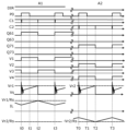
- FIG. 2 shows the polarity instruction signal DIR, the reference pulse signal P0, the first comparison signal C1, the second comparison signal C2, the output signal Q61 of the D flip-flop 61, and the output signal of the D flip-flop 63 in sections A1 and A2 of FIG. 1B.
- It is a graph showing an example of the waveforms of the output signal Q63, the output signal Q71 of the D flip-flop 71, the output signal Q73 of the D flip-flop 73, the drive signals V1 to V4, the current detection voltage Vs, and the motor current IL.
- the horizontal axis in FIG. 2 indicates time.
- 3A and 3B are state diagrams showing the state of each switch element and the current path in sections A1 and A2 of FIG. 1B, respectively.
- the inverted signal of the second reference pulse signal P2 which is a clock input, is fixed at a high level, so the output signal Q63 is maintained at a low level (L). Furthermore, since the second reference pulse signal P2 is at a low level, the output signal Q71 of the D flip-flop 71 having no clock input is maintained at a low level. The output signal Q73 of the D flip-flop 73 whose D terminal receives the inverted signal of the second comparison signal C2 at a high level is also maintained at a low level.
- the drive signal V2 which is the logical sum of the two, is also maintained at a low level, and the second high-side switch element 22 is in an off state and the second low-side switch element 24 is in an on state.
- the first high-side switch element 21 is turned on, a flow flows from the positive electrode of the input power source 1 to the first high-side switch element 21, the motor 3, the second low-side switch element 24, the current detection resistor 4, and the negative electrode of the input power source 1. Since the current increases while oscillating like a surge, the current detection voltage Vs also oscillates, and the first comparison signal C1 also oscillates between a high level and a low level.
- the current detection voltage Vs is ORed with the high level of the first reference pulse signal P1 in the OR circuit 62, and NANDed with the low level of the delayed signal of the delay circuit 78, which will be described later, in the NAND circuit 77. , does not affect circuit operation.
- This state is maintained at least until time t1 when the first reference pulse signal P1 is at a high level, and the motor current IL of the motor 3 to which the power supply voltage is applied in the positive direction increases in the positive direction.
- the pulse duration time of the reference pulse signal P0 is the minimum on-period Tm, which is the minimum value of the mask period.
- the first reference pulse signal P1 falls together with the reference pulse signal P0.
- the current detection voltage Vs has not reached the first reference waveform signal Vr1 and the first comparison signal C1 remains at a high level, so the D flip-flop 61 is not reset and the state is maintained until time t2. be done. That is, each switch element etc. is maintained in the state shown in state diagram (a) in FIG. 3A from time t0 to t2.
- the second high-side switch element 22 is fixed in the off state and the second low-side switch element 24 is fixed in the on state, and the first high-side switch element 22 is fixed in the on state at a predetermined switching period.
- the side switch element 21 and the first low side switch element 23 are alternately turned on and off.
- the on-period of the first high-side switch element 21 is controlled to be longer than the minimum on-period Tm and until the peak value of the motor current IL reaches the target waveform value Vr1/Rs.
- Section A2 in FIG. 1B is a section near the peak value in which the sign of the reference waveform signal is reversed with respect to the above-mentioned section A1, and the operation is performed by switching the roles of the first PWM circuit 6 and the second PWM circuit 7, and as described above.
- the times t0 to t3 of the interval A1 correspond to the times T0 to T3 of the interval A2. That is, the first high-side switch element 21 is fixed in the OFF state, the first low-side switch element 23 is fixed in the ON state, and the second high-side switch element 22 and the second low-side switch element 24 are switched on at a predetermined switching period. Turn on and off alternately.
- the on-period of the second high-side switch element 22 is controlled to be longer than the minimum on-period Tm and until the peak value of the motor current IL reaches the target waveform value Vr2/Rs.
- Each switch element etc. is maintained in the state shown in the state diagram (a) of FIG. 3B from time T0 to T2, and is maintained in the state shown in the state diagram (b) of FIG. 3B from time T2 to T3. be done.
- FIG. 4 shows the polarity instruction signal DIR, the reference pulse signal P0, the first comparison signal C1, the second comparison signal C2, the output signal Q61 of the D flip-flop 61, and the output signal of the D flip-flop 63 in section B of FIG. 1B.
- 7 is a graph showing an example of waveforms of Q63, output signal Q71 of D flip-flop 71, output signal Q73 of D flip-flop 73, drive signals V1 to V4, current detection voltage Vs, and motor current IL.
- FIG. 5 is a state diagram showing the state of each switch element and the path of flowing current in section B of FIG. 1B.
- the first reference pulse signal P1 falls in accordance with the reference pulse signal P0 with the motor current IL exceeding the control target value.
- the D flip-flop 61 is reset and the output signal Q61 falls. Therefore, the drive signal V1 also falls, the first high-side switch element 21 is turned off, and the first low-side switch element 23 is turned on.
- the D flip-flop 73 is clocked at the falling edge of the first reference pulse signal P1 while a high-level signal, which is an inverted signal of the first comparison signal C1, is applied to the D terminal, so that the D flip-flop 73 outputs an output signal.
- the output signal Q73 of the D flip-flop 73 is input to the reset terminal of the D flip-flop 73 via the delay circuit 78 and the NAND circuit 77.
- the output of the delay circuit 78 falls, but since the motor current IL is still higher than the control target value and the inverted signal of the second comparison signal C2 is at a low level, the output of the NAND circuit 77 is The output is maintained at a high level, the D flip-flop 73 is not reset, and the state of each switch element is maintained.
- the level of the first reference waveform signal Vr1 is also low, and when the minimum on-period Tm is reached at time t8 and the reference pulse signal P0 and the first reference pulse signal P1 fall, the motor current IL exceeds the control target value.
- the first high-side switch element 21 is turned off, and the state of each switch element returns to the fast decay state shown in the state diagram (b) of FIG. 5.
- the motor current IL falls below the control target value -Vr2/Rs (the current detection voltage Vs exceeds the second reference waveform signal Vr2), and the second comparison signal C2 falls.
- the delayed signal of the output signal Q73 of the D flip-flop 73 has not arrived, so the state remains unchanged.
- the D flip-flop 73 is reset and the output signal Q73 falls, the second high-side switch element 22 is turned off, and each switch The state of the element returns to the slow decay state shown in FIG. 5 (c). That is, the delay time of the output signal Q73 of the D flip-flop 73 by the delay circuit 78 is the minimum period of the fast decay state. Thereafter, such operations are repeated, and the motor current IL converges to the target waveform.
- FIG. 6 shows the polarity instruction signal DIR, the reference pulse signal P0, the first comparison signal C1, the second comparison signal C2, the output signal Q61 of the D flip-flop 61, and the output signal of the D flip-flop 63 in the section C of FIG. 1B.
- 7 is a graph showing an example of waveforms of Q63, output signal Q71 of D flip-flop 71, output signal Q73 of D flip-flop 73, drive signals V1 to V4, current detection voltage Vs, and motor current IL.
- Section C is a region where the polarity instruction signal DIR changes from a high level to a low level and the motor current IL should cross zero, and the first reference waveform signal Vr1 and the second reference waveform signal Vr2 are approximately zero.
- the drive signal V1 also rises, and the first high-side switch element 21 is turned on.
- the drive signal V2 falls and the first low-side switch element 23 is turned off. Since the first reference waveform signal Vr1 and the second reference waveform signal Vr2 are approximately zero, the first comparison signal C1 and the second comparison signal C2 are at a low level.
- the D flip-flop 61 is reset and the drive signal V1 becomes low level together with the output signal Q61, and the first high-side switch element 21 is turned off, and the first low-side switch element 23 is turned on.
- the D flip-flop 73 is clocked by the falling edge of the first reference pulse signal P1, and raises the output signal Q73.
- the drive signal V2 also becomes high level
- the second high-side switch element 22 is turned on
- the second low-side switch element 24 is turned off.
- the state of each switch element shifts from the state shown in FIG. 5 (a) to the fast decay state shown in state diagram (b).
- the motor current IL decreases, the current detection voltage Vs becomes negative, and the first comparison signal C1 and the second comparison signal C2 become high level.
- the time t13 is set to be after the delay time of the delay circuit 78, there is a possibility that the motor current IL reaches zero first, and then the delay time passes and the state of each switch element shifts to the slow decay state. . In that case, the motor current IL flows in a negative direction, but the motor current IL attenuates in a slow decay state. Although it depends on the characteristics and state of the motor 3, it is assumed that the back electromotive voltage is small near the zero cross, and the motor current IL in the slow decay state is also attenuated to zero or a small value.
- the first comparison signal C1 and the second comparison signal C2 are undefined.
- the first comparison signal C1 and the second comparison signal C2 are not referred to, and there is no effect on the operation. If it is desired to avoid this undefined state, hysteresis or offset may be set in the first comparison circuit 55 and the second comparison circuit 56.
- the state changes so that the first reference pulse signal P1 is fixed at a low level and the reference pulse signal P0 is output as the second reference pulse signal P2.
- the clock is input to the D flip-flop 71, the output signal Q71 rises, and the drive signal V2 rises via the OR circuits 70 and 76. Therefore, the second high-side switch element 22 is turned on and the second low-side switch element 24 is turned off. Power supply voltage Vcc is applied to the motor 3 in the negative direction, and the motor current IL increases in the negative direction.
- the second high-side switch element 22 is turned off, the first high-side switch element 21 is turned on, and the state of each switch element changes to fast decay, and at time t17, the first high-side switch element 22 turns off.
- the switch element 21 turns off and enters a slow decay state.
- the above operation differs in that the role is transferred from the first PWM circuit 6 to the second PWM circuit 7, but it is the same operation as described above, and the motor current IL smoothly reverses polarity. go.
- the motor current IL supplied from the input power source 1 is detected and the first target waveform value Vr1/Rs is set in the positive direction, and the first target waveform value Vr1/Rs is set in the negative direction.
- the peak current control to follow the target waveform value Vr2/Rs of 2
- the target current when the target current is exceeded during the minimum on period Tm, by providing a period in which the fast decay state occurs until the current decreases to the target current, the target current can be maintained even near the zero cross.
- the current waveform can be maintained.
- the motor drive device according to the present embodiment differs from the motor drive device 10 according to the first embodiment mainly in that the reference waveform generation circuit generates only one reference waveform signal.
- the motor drive device according to the present embodiment will be described below with reference to FIGS. 7A to 10, focusing on the differences from the motor drive device 10 according to the first embodiment.
- FIG. 7A is a circuit configuration diagram of motor drive device 110 according to this embodiment.
- the same components as in FIG. 1A are given the same reference numerals, and their description will be omitted.
- the motor drive device 110 includes a first series switch circuit 31, a second series switch circuit 32, a reference pulse generation circuit 50, and a current detection resistor 4. , a PWM circuit 5A, a reference waveform generation circuit 51A, and a current comparison circuit 57.
- motor drive device 110 further includes an amplifier 40, resistors 41, 42, 44, and 45, and a switch 43.
- the reference waveform generation circuit 51A generates a reference waveform signal Vr with a signal level of 0 or more.
- the reference waveform signal Vr will be explained using FIG. 7B.
- FIG. 7B is a graph showing an example of the waveforms of the polarity instruction signal DIR and the reference waveform signal Vr according to the present embodiment.
- Graph (a) in FIG. 7B is a graph showing an example of the waveform of the polarity instruction signal DIR.
- Graph (b) in FIG. 7B is a graph showing an example of the waveform of the reference waveform signal Vr.
- the horizontal axis of each graph represents time.
- the reference waveform signal Vr maintains a signal level of 0 or more and does not include a negative signal.
- the PWM circuit 5A includes a first switching circuit 58 and a second switching circuit 59 in addition to the same circuits as the first PWM circuit 6 according to the first embodiment.
- the PWM circuit 5A receives a reference pulse signal P0 instead of the first reference pulse signal P1 and the second reference pulse signal P2 according to the first embodiment. Further, the PWM circuit 5A does not include the OR circuit 66, and the output of the OR circuit 60 and the output signal Q63 of the D flip-flop 63 are input to the first switching circuit 58 and the second switching circuit 59.
- the first switching circuit 58 outputs the first drive signal to the first series switch circuit 31 mainly during a first period in which the motor current IL flows from the first connection point X1 to the second connection point X2. , is a circuit that outputs an output to the second series switch circuit 32 mainly during the second period when the motor current IL flows from the second connection point X2 to the first connection point X1.
- the first switching circuit 58 receives the polarity instruction signal DIR from the reference waveform generation circuit 51A, the output signal of the OR circuit 60, and the output signal Q63 of the D flip-flop 63, and selects the polarity instruction signal DIR according to the polarity instruction signal DIR.
- the output signal of the OR circuit 60 or the output signal Q63 of the D flip-flop 63 is output to the serial switch circuit 31 of No. 1.
- the second switching circuit 59 outputs the second drive signal to the second series switch circuit 32 mainly during the first period in which the motor current IL flows from the first connection point X1 to the second connection point X2.
- the second switching circuit 59 receives the polarity instruction signal DIR from the reference waveform generation circuit 51A, the output signal of the OR circuit 60, and the output signal Q63 of the D flip-flop 63, and selects the polarity instruction signal DIR according to the polarity instruction signal DIR.
- the output signal of the OR circuit 60 or the output signal Q63 of the D flip-flop 63 is output to the serial switch circuit 31 of No. 1.
- the output of the OR circuit 60 of the PWM circuit 5A becomes the drive signal V1 via the first switching circuit 58 when the polarity instruction signal DIR is at a high level, and becomes the drive signal V1 via the first switching circuit 58 when the polarity instruction signal DIR is at a low level. 59 to become the drive signal V2.
- the output signal Q63 of the D flip-flop 63 becomes the drive signal V2 via the second switching circuit 59, and when the polarity instruction signal DIR is at a low level, it becomes the drive signal V2 through the first switching circuit. 58 to become the drive signal V1.
- the objects to be compared in the current comparison circuit 57 are also different from those in the first embodiment.
- the current detection voltage Vs of the current detection resistor 4 and the first reference waveform signal Vr1 were compared, but in this embodiment, the reference waveform signal Vr is once amplified N times by the amplifier 40, and then the current detection voltage Vs of the current detection resistor 4 is compared with the first reference waveform signal Vr1. and the resistor 42 and return it to the reference waveform signal Vr, which is then input to the current comparison circuit 57.
- the detection voltage VsA obtained from the voltage Vs of the current detection resistor 4 via the resistor 45 having a resistance value R5 is input to the current comparison circuit 57, and is compared with the reference waveform signal (divided voltage) Vr to generate a comparison signal C3. is output. Furthermore, a series circuit of a switch 43 that opens and closes in response to the output signal Q63 of the D flip-flop 63 and a resistor 44 having a resistance value R4 is connected between the output of the amplifier 40 (voltage N ⁇ Vr) and a resistor 45 (voltage VsA). be done.
- the comparison signal C3 output by the current comparison circuit 57 is the comparison result between the current detection voltage Vs and the reference waveform signal Vr.
- the switch 43 when the output signal Q63 of the D flip-flop 63 is at a high level, that is, in the fast decay state, the switch 43 is in the on state, and the detection voltage VsA is biased by the output N ⁇ Vr of the amplifier 40, as shown in the following equation. become.
- VsA (R4 ⁇ Vs+R5 ⁇ N ⁇ Vr)/(R4+R5)
- Vs ⁇ 1-(N-1) ⁇ R5/R4 ⁇ Vr
- the current comparison circuit 57 Equivalently, the current detection voltage Vs (that is, the current signal) is compared with a signal obtained by negatively inverting the reference waveform signal Vr.
- FIG. 8 shows the polarity instruction signal DIR, reference pulse signal P0, comparison signal C3, output signal Q61 of the D flip-flop 61, output signal Q63 of the D flip-flop 63, drive signals V1 to V4, in the sections A1 and A2 of FIG. 7B, It is a graph showing an example of waveforms of current detection voltage Vs and motor current IL. The state of each switch element and the path of the flowing current are the same as in FIGS. 3A and 3B. The operation near the reference waveform peak will be described below with reference to FIGS. 7A, 7B, and 8.
- the drive signal V1 When the polarity instruction signal DIR is at a high level, that is, the motor current IL is in the positive direction, and the reference pulse signal P0 rises at time t0, the drive signal V1 also rises via the OR circuit 60 and the first switching circuit 58. The first high-side switch element 21 is turned on. At the same time, the drive signal V2 falls and the first low-side switch element 23 is turned off. Since the reference pulse signal P0 is clocked into the D flip-flop 61 while the high-level comparison signal C3 is input to the reset terminal, the output signal Q61 of the D flip-flop 61 also rises.
- the output signal Q63 of the D flip-flop 63 which receives the inverted signal of the comparison signal C3 at a high level and is input to the D terminal, is at a low level, and the output signal Q63 becomes the drive signal V2 via the second switching circuit 59. Therefore, the second high-side switch element 22 is in an off state, and the second low-side switch element 24 is in an on state.
- the positive electrode of the input power source 1 is connected to the first high-side switch element 21, the motor 3, the second low-side switch element 24, the current detection resistor 4, and the negative electrode of the input power source 1.
- the current detection voltage Vs Since the flowing current increases while oscillating like a surge, the current detection voltage Vs also oscillates, and the comparison signal C3 also oscillates between a high level and a low level. However, the current detection voltage Vs is logically summed with the high level of the reference pulse signal P0 in the OR circuit 62, and NANDed with the low level of the delayed signal of the delay circuit 68, which will be described later, in the NAND circuit 67, so that the circuit operates. does not affect. This state is maintained at least until time t1 when the reference pulse signal P0 is at a high level, and the motor current IL of the motor 3 to which the power supply voltage is applied in the positive direction increases in the positive direction. As described above, the pulse duration time of the reference pulse signal P0 is the minimum on-period Tm, which is the minimum value of the mask period.
- the reference pulse signal P0 falls.
- the current detection voltage Vs has not reached the reference waveform signal Vr and the comparison signal C3 remains at a high level, so the D flip-flop 61 is not reset and the state is maintained until time t2.
- Each switch element etc. is maintained in the state shown in the state diagram (a) of FIG. 3A from time t0 to t2.
- the second high-side switch element 22 is fixed in the OFF state
- the second low-side switch element 24 is fixed in the ON state
- the first high-side switch element 22 is fixed in the ON state at a predetermined switching period.
- 21 and the first low-side switch element 23 are alternately turned on and off.
- the on-period of the first high-side switch element 21 is controlled to be longer than the minimum on-period Tm and until the peak value of the motor current IL reaches the target waveform value Vr/Rs.
- the PWM circuit 5A operates in the same manner as in section A1 described above, but since the polarity instruction signal DIR is at a low level, the states of the first switching circuit 58 and the second switching circuit 59 are different from those in the section A1.
- the output signal of the OR circuit 60 is the drive signal V2
- the output signal Q63 of the D flip-flop 63 is the drive signal V1.
- the time T0 to T3 of the section A2 corresponds to the time t0 to t3 of the above-mentioned section A1, and the first high side switch element 21 is fixed in the off state and the first low side switch element 23 is fixed in the on state, and a predetermined switching is performed.
- the second high-side switch element 22 and the second low-side switch element 24 are alternately turned on and off in cycles.
- the on period of the second high side switch element 22 is controlled to be longer than the minimum on period Tm and until the peak value of the motor current IL reaches the target waveform value Vr/Rs.
- Each switch element, etc. is maintained in the state shown in the state diagram (a) of FIG. 3B from time T0 to T2, and is maintained in the state shown in state diagram (b) of FIG. 3B from time T2 to T3.
- FIG. 9 shows the polarity instruction signal DIR, reference pulse signal P0, comparison signal C3, output signal Q61 of the D flip-flop 61, output signal Q63 of the D flip-flop 63, drive signals V1 to V4, and current detection in section B of FIG. 7B. It is a graph which shows an example of the waveform of voltage Vs and motor current IL. The state of each switch element and the path of the flowing current are similar to the state diagram shown in FIG. 5.
- the reference pulse signal P0 falls in accordance with the reference pulse signal P0 with the motor current IL exceeding the control target value Vr/Rs.
- the D flip-flop 61 is reset and the output signal Q61 falls. Therefore, the drive signal V1 also falls, the first high-side switch element 21 is turned off, and the first low-side switch element 23 is turned on. Further, the D flip-flop 63 is clocked at the falling edge of the reference pulse signal P0 while a high level signal, which is an inverted signal of the comparison signal C3, is input to the D terminal, so that the output signal Q63 rises.
- each switch element is the fast decay state shown in the state diagram (b) of FIG. 5, in which the current supplied from the input power source 1 and flowing through the current detection resistor 4 flows backward and becomes a regenerative current. Further, when the output signal Q63 of the D flip-flop 63 becomes high level, the switch 43 is turned on, and the comparison signal C3 becomes equivalently the result of comparison between the current detection voltage Vs and the negative reference waveform signal -Vr.
- the output signal Q63 of the D flip-flop 63 is input to the reset terminal of the D flip-flop 63 via the delay circuit 68 and the NAND circuit 67.
- the output of the delay circuit 68 falls, but since the motor current IL is still higher than the control target value and the inverted signal of the comparison signal C3 is at a low level, the output of the NAND circuit 67 is at a high level.
- the D flip-flop 63 is not reset and the state of the switch is maintained.
- the drive signal V1 When the reference pulse signal P0 rises at time t7, the drive signal V1 also rises via the OR circuit 60 and the first switching circuit 58, and the first high-side switch element 21 is turned on. At the same time, the drive signal V3 falls, the first low-side switch element 23 turns off, and the motor current IL of the motor 3 to which the power supply voltage Vcc is applied in the positive direction increases in the positive direction (state diagram in FIG. 5). (a)). Compared to the previous cycle, the motor current IL is attenuated due to the fast decay state, and the level of the current detection voltage Vs is also lowered.
- the D flip-flop 63 is reset and the output signal Q63 falls, and the second high-side switch element 22 is turned off and slow decays. state. That is, the delay time of the output signal Q63 of the D flip-flop 63 by the delay circuit 68 is the minimum period of the fast decay state. Thereafter, such operations are repeated, and the motor current IL converges to the target waveform.
- FIG. 10 shows the polarity instruction signal DIR, reference pulse signal P0, comparison signal C3, output signal Q61 of the D flip-flop 61, output signal Q63 of the D flip-flop 63, drive signals V1 to V4, and current detection in section C of FIG. 7B. It is a graph which shows an example of the waveform of voltage Vs and motor current IL.
- Section C is a region where the polarity instruction signal DIR changes from a high level to a low level and the motor current IL should cross zero, and the reference waveform signal Vr is approximately zero.
- the D flip-flop 61 is reset and the drive signal V1 becomes low level together with the output signal Q61, and the first high-side switch element 21 is turned off. state, and the first low-side switch element 23 is turned on.
- the D flip-flop 63 is clocked by the falling edge of the reference pulse signal P0, and raises the output signal Q63.
- the drive signal V2 also becomes high level, the second high-side switch element 22 is turned on, and the second low-side switch element 24 is turned off.
- time t13 is set after the delay time of the delay circuit 68, there may be a case where the motor current IL reaches zero first, and then the delay time passes and the state of the switch shifts to the slow decay state. In that case, the motor current IL flows in the negative direction, but the current attenuates in a slow decay state. Although it depends on the characteristics and state of the motor 3, it is assumed that the back electromotive voltage is small near the zero cross, and the motor current in the slow decay state is also attenuated to zero or a small value.
- the comparison signal C3 becomes undefined.
- the comparison signal C3 is not referred to, and there is no effect on the operation. If it is desired to avoid this unstable state, hysteresis or offset may be set in the current comparison circuit 57.
- the second high-side switch element 22 turns off, the first high-side switch element 21 turns on, and enters the fast decay state, and at time t17, the first high-side switch element 21 turns off. state and turns into a slow decay state.
- the polarity of the motor current IL is smoothly reversed.
- the motor current IL supplied from the input power source 1 is detected, and the target waveform value Vr/Rs is detected in the positive direction, and the target waveform value -
- the target current waveform is maintained even near zero cross by providing a period in which the current is in a fast decay state until it decreases to the target current. be able to.
- fast decay may be used instead of slow decay in normal operation, but fast decay increases the ripple of the motor current.
- An increase in ripple current leads to an increase in conduction loss and an increase in switching frequency noise due to an increase in the effective value of the current. Therefore, in the present disclosure, the fast decay state is provided only to correct the excess of the current target value during the minimum on-period.
- the high level and low level of each signal may be inverted, and the circuit configuration may be changed depending on each signal.
- the motor drive device of the present disclosure can be applied to motors for various uses including in-vehicle use, as a motor drive device that can drive a motor with low noise and low vibration, for example.
Landscapes
- Engineering & Computer Science (AREA)
- Power Engineering (AREA)
- Control Of Direct Current Motors (AREA)
Priority Applications (3)
| Application Number | Priority Date | Filing Date | Title |
|---|---|---|---|
| JP2024510187A JPWO2023182303A1 (https=) | 2022-03-25 | 2023-03-20 | |
| CN202380028590.6A CN118901200A (zh) | 2022-03-25 | 2023-03-20 | 电机驱动装置 |
| US18/807,297 US20240405706A1 (en) | 2022-03-25 | 2024-08-16 | Motor driver |
Applications Claiming Priority (2)
| Application Number | Priority Date | Filing Date | Title |
|---|---|---|---|
| JP2022050627 | 2022-03-25 | ||
| JP2022-050627 | 2022-03-25 |
Related Child Applications (1)
| Application Number | Title | Priority Date | Filing Date |
|---|---|---|---|
| US18/807,297 Continuation US20240405706A1 (en) | 2022-03-25 | 2024-08-16 | Motor driver |
Publications (1)
| Publication Number | Publication Date |
|---|---|
| WO2023182303A1 true WO2023182303A1 (ja) | 2023-09-28 |
Family
ID=88101057
Family Applications (1)
| Application Number | Title | Priority Date | Filing Date |
|---|---|---|---|
| PCT/JP2023/010992 Ceased WO2023182303A1 (ja) | 2022-03-25 | 2023-03-20 | モータ駆動装置 |
Country Status (4)
| Country | Link |
|---|---|
| US (1) | US20240405706A1 (https=) |
| JP (1) | JPWO2023182303A1 (https=) |
| CN (1) | CN118901200A (https=) |
| WO (1) | WO2023182303A1 (https=) |
Citations (3)
| Publication number | Priority date | Publication date | Assignee | Title |
|---|---|---|---|---|
| JP2018198533A (ja) * | 2018-09-11 | 2018-12-13 | セイコーエプソン株式会社 | 回路装置及び電子機器 |
| JP2018207607A (ja) * | 2017-05-31 | 2018-12-27 | ミネベアミツミ株式会社 | モータ電流制御装置およびモータ電流制御方法 |
| JP2020058120A (ja) * | 2018-10-01 | 2020-04-09 | ローム株式会社 | モータドライバ装置 |
-
2023
- 2023-03-20 JP JP2024510187A patent/JPWO2023182303A1/ja active Pending
- 2023-03-20 CN CN202380028590.6A patent/CN118901200A/zh active Pending
- 2023-03-20 WO PCT/JP2023/010992 patent/WO2023182303A1/ja not_active Ceased
-
2024
- 2024-08-16 US US18/807,297 patent/US20240405706A1/en active Pending
Patent Citations (3)
| Publication number | Priority date | Publication date | Assignee | Title |
|---|---|---|---|---|
| JP2018207607A (ja) * | 2017-05-31 | 2018-12-27 | ミネベアミツミ株式会社 | モータ電流制御装置およびモータ電流制御方法 |
| JP2018198533A (ja) * | 2018-09-11 | 2018-12-13 | セイコーエプソン株式会社 | 回路装置及び電子機器 |
| JP2020058120A (ja) * | 2018-10-01 | 2020-04-09 | ローム株式会社 | モータドライバ装置 |
Also Published As
| Publication number | Publication date |
|---|---|
| CN118901200A (zh) | 2024-11-05 |
| US20240405706A1 (en) | 2024-12-05 |
| JPWO2023182303A1 (https=) | 2023-09-28 |
Similar Documents
| Publication | Publication Date | Title |
|---|---|---|
| CN1316729C (zh) | 单相电动机驱动装置、单相电动机驱动方法 | |
| JP2007013916A (ja) | 信号生成装置 | |
| US8400095B2 (en) | Constant-speed control circuit for BLDC motors | |
| JP4582466B2 (ja) | モータ制御装置 | |
| JP5408893B2 (ja) | モータ駆動回路 | |
| JP2007043890A (ja) | ファンモーターの駆動装置 | |
| JP4268176B2 (ja) | フローティング駆動回路 | |
| CN103633919B (zh) | 电机控制装置 | |
| US20120112800A1 (en) | Method of and Driver Circuit for Operating a Semiconductor Power Switch | |
| WO2023182303A1 (ja) | モータ駆動装置 | |
| JP7174672B2 (ja) | スイッチング電源装置 | |
| US5825145A (en) | Quiet commutation circuit for an electric motor | |
| JP2015050876A (ja) | モータ駆動装置 | |
| JP5125218B2 (ja) | モータ制御装置 | |
| CN113644817B (zh) | 升压dc/dc转换器的过载保护电路 | |
| JPH08288811A (ja) | プッシュプル駆動回路 | |
| CN103633906B (zh) | 电机控制装置 | |
| JP7129366B2 (ja) | スイッチング電源装置 | |
| JP2003338743A (ja) | パワーデバイスの駆動回路 | |
| CN222073017U (zh) | 一种马达即停驱动电路及电路板 | |
| JP2008141831A (ja) | モータ駆動回路 | |
| JP2015035725A (ja) | 電磁負荷を駆動する装置及びシステム | |
| JP2004289946A (ja) | モーター駆動回路 | |
| JP2006352269A (ja) | パルス幅変調回路およびスイッチングアンプ | |
| KR100290117B1 (ko) | 3상 스텝 모터의 마이크로 스텝 구동회로 |
Legal Events
| Date | Code | Title | Description |
|---|---|---|---|
| 121 | Ep: the epo has been informed by wipo that ep was designated in this application |
Ref document number: 23774898 Country of ref document: EP Kind code of ref document: A1 |
|
| ENP | Entry into the national phase |
Ref document number: 2024510187 Country of ref document: JP Kind code of ref document: A |
|
| WWE | Wipo information: entry into national phase |
Ref document number: 202380028590.6 Country of ref document: CN |
|
| NENP | Non-entry into the national phase |
Ref country code: DE |
|
| 122 | Ep: pct application non-entry in european phase |
Ref document number: 23774898 Country of ref document: EP Kind code of ref document: A1 |