WO2023180859A1 - 半導体装置及び半導体装置の作製方法 - Google Patents
半導体装置及び半導体装置の作製方法 Download PDFInfo
- Publication number
- WO2023180859A1 WO2023180859A1 PCT/IB2023/052379 IB2023052379W WO2023180859A1 WO 2023180859 A1 WO2023180859 A1 WO 2023180859A1 IB 2023052379 W IB2023052379 W IB 2023052379W WO 2023180859 A1 WO2023180859 A1 WO 2023180859A1
- Authority
- WO
- WIPO (PCT)
- Prior art keywords
- insulator
- conductor
- oxide
- semiconductor device
- film
- Prior art date
- Legal status (The legal status is an assumption and is not a legal conclusion. Google has not performed a legal analysis and makes no representation as to the accuracy of the status listed.)
- Ceased
Links
Images


Classifications
-
- H—ELECTRICITY
- H10—SEMICONDUCTOR DEVICES; ELECTRIC SOLID-STATE DEVICES NOT OTHERWISE PROVIDED FOR
- H10B—ELECTRONIC MEMORY DEVICES
- H10B12/00—Dynamic random access memory [DRAM] devices
- H10B12/30—DRAM devices comprising one-transistor - one-capacitor [1T-1C] memory cells
-
- H—ELECTRICITY
- H10—SEMICONDUCTOR DEVICES; ELECTRIC SOLID-STATE DEVICES NOT OTHERWISE PROVIDED FOR
- H10B—ELECTRONIC MEMORY DEVICES
- H10B12/00—Dynamic random access memory [DRAM] devices
- H10B12/01—Manufacture or treatment
- H10B12/02—Manufacture or treatment for one transistor one-capacitor [1T-1C] memory cells
- H10B12/05—Making the transistor
-
- H—ELECTRICITY
- H10—SEMICONDUCTOR DEVICES; ELECTRIC SOLID-STATE DEVICES NOT OTHERWISE PROVIDED FOR
- H10B—ELECTRONIC MEMORY DEVICES
- H10B12/00—Dynamic random access memory [DRAM] devices
-
- H—ELECTRICITY
- H10—SEMICONDUCTOR DEVICES; ELECTRIC SOLID-STATE DEVICES NOT OTHERWISE PROVIDED FOR
- H10B—ELECTRONIC MEMORY DEVICES
- H10B12/00—Dynamic random access memory [DRAM] devices
- H10B12/01—Manufacture or treatment
- H10B12/02—Manufacture or treatment for one transistor one-capacitor [1T-1C] memory cells
- H10B12/03—Making the capacitor or connections thereto
- H10B12/033—Making the capacitor or connections thereto the capacitor extending over the transistor
-
- H—ELECTRICITY
- H10—SEMICONDUCTOR DEVICES; ELECTRIC SOLID-STATE DEVICES NOT OTHERWISE PROVIDED FOR
- H10B—ELECTRONIC MEMORY DEVICES
- H10B12/00—Dynamic random access memory [DRAM] devices
- H10B12/30—DRAM devices comprising one-transistor - one-capacitor [1T-1C] memory cells
- H10B12/31—DRAM devices comprising one-transistor - one-capacitor [1T-1C] memory cells having a storage electrode stacked over the transistor
-
- H—ELECTRICITY
- H10—SEMICONDUCTOR DEVICES; ELECTRIC SOLID-STATE DEVICES NOT OTHERWISE PROVIDED FOR
- H10B—ELECTRONIC MEMORY DEVICES
- H10B41/00—Electrically erasable-and-programmable ROM [EEPROM] devices comprising floating gates
- H10B41/70—Electrically erasable-and-programmable ROM [EEPROM] devices comprising floating gates the floating gate being an electrode shared by two or more components
-
- H—ELECTRICITY
- H10—SEMICONDUCTOR DEVICES; ELECTRIC SOLID-STATE DEVICES NOT OTHERWISE PROVIDED FOR
- H10B—ELECTRONIC MEMORY DEVICES
- H10B99/00—Subject matter not provided for in other groups of this subclass
-
- H—ELECTRICITY
- H10—SEMICONDUCTOR DEVICES; ELECTRIC SOLID-STATE DEVICES NOT OTHERWISE PROVIDED FOR
- H10D—INORGANIC ELECTRIC SEMICONDUCTOR DEVICES
- H10D30/00—Field-effect transistors [FET]
- H10D30/01—Manufacture or treatment
- H10D30/021—Manufacture or treatment of FETs having insulated gates [IGFET]
-
- H—ELECTRICITY
- H10—SEMICONDUCTOR DEVICES; ELECTRIC SOLID-STATE DEVICES NOT OTHERWISE PROVIDED FOR
- H10D—INORGANIC ELECTRIC SEMICONDUCTOR DEVICES
- H10D30/00—Field-effect transistors [FET]
- H10D30/60—Insulated-gate field-effect transistors [IGFET]
- H10D30/67—Thin-film transistors [TFT]
-
- H—ELECTRICITY
- H10—SEMICONDUCTOR DEVICES; ELECTRIC SOLID-STATE DEVICES NOT OTHERWISE PROVIDED FOR
- H10D—INORGANIC ELECTRIC SEMICONDUCTOR DEVICES
- H10D30/00—Field-effect transistors [FET]
- H10D30/60—Insulated-gate field-effect transistors [IGFET]
- H10D30/67—Thin-film transistors [TFT]
- H10D30/6729—Thin-film transistors [TFT] characterised by the electrodes
- H10D30/673—Thin-film transistors [TFT] characterised by the electrodes characterised by the shapes, relative sizes or dispositions of the gate electrodes
-
- H—ELECTRICITY
- H10—SEMICONDUCTOR DEVICES; ELECTRIC SOLID-STATE DEVICES NOT OTHERWISE PROVIDED FOR
- H10D—INORGANIC ELECTRIC SEMICONDUCTOR DEVICES
- H10D30/00—Field-effect transistors [FET]
- H10D30/60—Insulated-gate field-effect transistors [IGFET]
- H10D30/67—Thin-film transistors [TFT]
- H10D30/674—Thin-film transistors [TFT] characterised by the active materials
- H10D30/6755—Oxide semiconductors, e.g. zinc oxide, copper aluminium oxide or cadmium stannate
-
- H—ELECTRICITY
- H10—SEMICONDUCTOR DEVICES; ELECTRIC SOLID-STATE DEVICES NOT OTHERWISE PROVIDED FOR
- H10D—INORGANIC ELECTRIC SEMICONDUCTOR DEVICES
- H10D30/00—Field-effect transistors [FET]
- H10D30/60—Insulated-gate field-effect transistors [IGFET]
- H10D30/67—Thin-film transistors [TFT]
- H10D30/6757—Thin-film transistors [TFT] characterised by the structure of the channel, e.g. transverse or longitudinal shape or doping profile
-
- H—ELECTRICITY
- H10—SEMICONDUCTOR DEVICES; ELECTRIC SOLID-STATE DEVICES NOT OTHERWISE PROVIDED FOR
- H10D—INORGANIC ELECTRIC SEMICONDUCTOR DEVICES
- H10D84/00—Integrated devices formed in or on semiconductor substrates that comprise only semiconducting layers, e.g. on Si wafers or on GaAs-on-Si wafers
- H10D84/01—Manufacture or treatment
- H10D84/0123—Integrating together multiple components covered by H10D12/00 or H10D30/00, e.g. integrating multiple IGBTs
- H10D84/0126—Integrating together multiple components covered by H10D12/00 or H10D30/00, e.g. integrating multiple IGBTs the components including insulated gates, e.g. IGFETs
-
- H—ELECTRICITY
- H10—SEMICONDUCTOR DEVICES; ELECTRIC SOLID-STATE DEVICES NOT OTHERWISE PROVIDED FOR
- H10D—INORGANIC ELECTRIC SEMICONDUCTOR DEVICES
- H10D84/00—Integrated devices formed in or on semiconductor substrates that comprise only semiconducting layers, e.g. on Si wafers or on GaAs-on-Si wafers
- H10D84/01—Manufacture or treatment
- H10D84/02—Manufacture or treatment characterised by using material-based technologies
- H10D84/03—Manufacture or treatment characterised by using material-based technologies using Group IV technology, e.g. silicon technology or silicon-carbide [SiC] technology
- H10D84/038—Manufacture or treatment characterised by using material-based technologies using Group IV technology, e.g. silicon technology or silicon-carbide [SiC] technology using silicon technology, e.g. SiGe
-
- H—ELECTRICITY
- H10—SEMICONDUCTOR DEVICES; ELECTRIC SOLID-STATE DEVICES NOT OTHERWISE PROVIDED FOR
- H10D—INORGANIC ELECTRIC SEMICONDUCTOR DEVICES
- H10D84/00—Integrated devices formed in or on semiconductor substrates that comprise only semiconducting layers, e.g. on Si wafers or on GaAs-on-Si wafers
- H10D84/80—Integrated devices formed in or on semiconductor substrates that comprise only semiconducting layers, e.g. on Si wafers or on GaAs-on-Si wafers characterised by the integration of at least one component covered by groups H10D12/00 or H10D30/00, e.g. integration of IGFETs
- H10D84/82—Integrated devices formed in or on semiconductor substrates that comprise only semiconducting layers, e.g. on Si wafers or on GaAs-on-Si wafers characterised by the integration of at least one component covered by groups H10D12/00 or H10D30/00, e.g. integration of IGFETs of only field-effect components
- H10D84/83—Integrated devices formed in or on semiconductor substrates that comprise only semiconducting layers, e.g. on Si wafers or on GaAs-on-Si wafers characterised by the integration of at least one component covered by groups H10D12/00 or H10D30/00, e.g. integration of IGFETs of only field-effect components of only insulated-gate FETs [IGFET]
-
- H—ELECTRICITY
- H10—SEMICONDUCTOR DEVICES; ELECTRIC SOLID-STATE DEVICES NOT OTHERWISE PROVIDED FOR
- H10W—GENERIC PACKAGES, INTERCONNECTIONS, CONNECTORS OR OTHER CONSTRUCTIONAL DETAILS OF DEVICES COVERED BY CLASS H10
- H10W20/00—Interconnections in chips, wafers or substrates
- H10W20/01—Manufacture or treatment
-
- H—ELECTRICITY
- H10—SEMICONDUCTOR DEVICES; ELECTRIC SOLID-STATE DEVICES NOT OTHERWISE PROVIDED FOR
- H10W—GENERIC PACKAGES, INTERCONNECTIONS, CONNECTORS OR OTHER CONSTRUCTIONAL DETAILS OF DEVICES COVERED BY CLASS H10
- H10W20/00—Interconnections in chips, wafers or substrates
- H10W20/40—Interconnections external to wafers or substrates, e.g. back-end-of-line [BEOL] metallisations or vias connecting to gate electrodes
Definitions
- the sixth conductor of the memory cell has the same material as the eighth conductor of the first memory cell, and in a cross-sectional view of the transistor, one of the side ends of the third conductor is , substantially coincides with one of the side edges of the metal oxide, and one of the side edges of the fourth conductor substantially coincides with the other side edge of the metal oxide.
- a seventh insulator that covers the third conductor, the fourth conductor, the metal oxide, and the third insulator, and the seventh insulator is the third conductor.
- a first opening overlapping a region sandwiched between the body and the fourth conductor; a second opening overlapping the opening of the first insulator; and a second opening overlapping the opening of the first insulator;
- At least a portion of a second insulator and a fifth conductor are disposed within the first opening
- a seventh conductor and a fourth insulator are disposed within the second opening of the seventh insulator.
- at least a portion of the eighth conductor are preferably arranged.
- ordinal numbers such as “first” and “second” are used for convenience, and do not limit the number of components or the order of the components (for example, the order of steps or the order of lamination). It's not something you do. Further, the ordinal number attached to a constituent element in a certain part of this specification may not match the ordinal number attached to the constituent element in another part of this specification or in the claims.
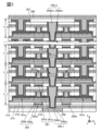
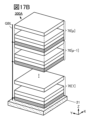
- each layer from the second layer onwards has a similar configuration, so in this embodiment, the second layer 11_2 will mainly be described as an example. Further, regarding the first layer 11_1, descriptions of parts similar to those of the second layer 11_2 will be omitted, and parts different from the second layer 11_2 will be mainly described.
- the first layer 11_1 includes transistors 202a and 202b and capacitive elements 101a and 101b.
- the second layer 11_2 includes transistors 201a and 201b and capacitive elements 101a and 101b.
- Each layer from the third layer 11_3 to the m-th layer 11_m also includes transistors 201a and 201b and capacitive elements 101a and 101b.
- the first layer 11_1 and the second layer 11_2 have a configuration on the right side and a configuration on the left side, respectively, which are symmetrical with respect to the conductor 240. That is, in FIG. 1, the transistor 201a and the transistor 201b are symmetrical, the transistor 202a and the transistor 202b are symmetrical, and the capacitor 101a and the capacitor 101b are symmetrical.
- the structure on the left side of the first layer 11_1 and the second layer 11_2 (transistors 201a, 202a, and capacitor 101a) will be mainly described as an example.
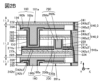
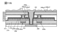
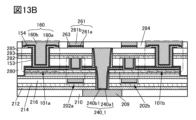
- the transistor 201a includes a conductor 261 (conductor 261a and conductor 261b) embedded in an insulator 284, an insulator 222 on the conductor 261, an insulator 224 on the insulator 222, and The oxide 230 (oxide 230a and oxide 230b) on the body 224, the conductor 242a (conductor 242a1 and conductor 242a2) and the conductor 242b (conductor 242b1 and conductor 242b2) on the oxide 230, , an insulator 271a on the conductor 242a, an insulator 271b on the conductor 242b, an insulator 250 on the oxide 230, and a conductor 260 on the insulator 250 (conductor 260a and conductor 260b), has.
- An insulator 275 is provided on the insulators 271a and 271b, and an insulator 280 is provided on the insulator 275. Insulator 250 and conductor 260 are embedded in openings provided in insulator 280 and insulator 275.
- An insulator 282 is provided on the insulator 280 and on the conductor 260. Further, an insulator 283 is provided on the insulator 282, and an insulator 285 is provided on the insulator 283. Further, an insulator 284 is provided on the insulator 285.
- one of the side ends of the conductor 242a approximately coincides with one of the side ends of the oxide 230, and one of the side ends of the conductor 242b is Preferably, it approximately coincides with the other side edge of the oxide 230. Furthermore, it is preferable that the side edges of the insulator 224 substantially coincide with the side edges of the oxide 230. In one embodiment of the present invention, the insulator 224, the oxide 230, and the conductor that will become the conductor 242a and the conductor 242b in a later step can be processed into an island shape all at once. Accordingly, a semiconductor device according to one embodiment of the present invention can be manufactured with good productivity.
- the insulator 271a and the insulator 271b are films that protect the conductor 242a and the conductor 242b during the island-shaped processing.
- the insulator 271a and the insulator 271b function as etching stoppers when removing the hard mask in processing the conductor 242a and the conductor 242b. Therefore, as shown in FIG. 2A, in a cross-sectional view of the transistor 201a, the side end of the insulator 271a on the insulator 250 side approximately coincides with the side end of the conductor 242a on the insulator 250 side, and the insulator 271b It is preferable that both side ends of the conductor 242b substantially coincide with the side ends of the conductor 242b.
- the stacked layers will be different from each other in the top view. It can be said that at least part of the outlines overlap. For example, this includes a case where the lower part of the side edge of the upper layer contacts the upper part of the side edge of the lower layer.
- the upper layer and the lower layer include a case where the upper layer and the lower layer are processed using the same mask pattern or partially the same mask pattern.
- the outlines do not overlap, and part of the upper layer may be located inside the lower layer, or part of the upper layer may be located outside the lower layer, and in this case, the side edges are approximately the same. It is said that they match, or that their top surface shapes roughly match.
- the capacitive element 101a includes a conductor 153 on a conductor 242b, an insulator 154 on the conductor 153, and a conductor 160 (conductor 160a and conductor 160b) on the insulator 154.
- the conductor 153, the insulator 154, and the conductor 160 each have at least a portion formed in an opening provided in the insulator 271b, the insulator 275, the insulator 280, the insulator 282, the insulator 283, and the insulator 285. is located inside.
- the ends of each of the conductor 153, the insulator 154, and the conductor 160 are located at least on the insulator 282, and preferably on the insulator 285.
- the insulator 154 is provided to cover the end of the conductor 153. Thereby, the conductor 153 and the conductor 160 can be electrically insulated.
- the conductor 242b provided in an overlapping manner on the oxide 230 functions as a wiring electrically connected to the conductor 153 of the capacitive element 101a.
- the conductor 242a provided overlappingly on the oxide 230 functions as a wiring electrically connected to the conductor 240.
- the upper surface and side end portions of the conductor 242a are electrically connected to the conductor 240_2 extending in the Z direction.
- the conductor 240_2 directly contacts at least one of the top surface and side end portion of the conductor 242a, there is no need to provide a separate connection electrode, so the area occupied by the memory array can be reduced. Furthermore, the degree of integration of memory cells is improved, and storage capacity can be increased. Note that it is preferable that the conductor 240_2 be in contact with a part of the upper surface and the side end portion of the conductor 242a. The contact resistance between the conductor 240_2 and the conductor 242a can be reduced by the conductor 240_2 being in contact with multiple surfaces of the conductor 242a.
- the width W2 is preferably larger than the width W1.
- the conductor 240_2 contacts at least a portion of the upper surface and a portion of the side end portion of the conductor 242a. Therefore, the area of the region where the conductor 240_2 and the conductor 242a are in contact can be increased. Note that in this specification and the like, the contact between the conductor 240_2 and the conductor 242a shown in FIG. 4A and the like may be referred to as a top side contact.
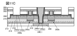
- an insulator 241 is provided in contact with the side surface of the conductor 240 (for example, the conductor 240_2 corresponds to this in FIGS. 4A and 4B).
- the insulator 241 includes a conductor 240_2, an insulator 284, an insulator 222, an insulator 224, an oxide 230, an insulator 271a, an insulator 275, an insulator 280, an insulator 282, the insulator 283, and the insulator 285.
- the conductor 242a is exposed from the insulator 241 and is in contact with the conductor 240_2.
- the insulator 241 can prevent impurities such as hydrogen and oxygen contained in the conductor 240_2 from diffusing into the oxide 230. Thereby, the electrical characteristics and reliability of the transistor 201a can be improved.
- the components of the transistor 201a will be mainly described below as an example, the description can also be applied to the components of the transistor 202a.
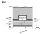
- the oxide 230 preferably includes an oxide 230a on the insulator 224 and an oxide 230b on the oxide 230a. By having the oxide 230a below the oxide 230b, diffusion of impurities from a structure formed below the oxide 230a to the oxide 230b can be suppressed.
- the oxide 230 has a two-layer structure of the oxide 230a and the oxide 230b
- the structure is not limited thereto.
- the oxide 230 may have a single layer structure of the oxide 230b, or may have a stacked structure of three or more layers.
- the region 230bc has fewer oxygen vacancies or has a lower impurity concentration than the regions 230ba and 230bb, so it is a high resistance region with a lower carrier concentration. Therefore, the region 230bc can be said to be i-type (intrinsic) or substantially i-type.
- the carrier concentration of the region 230bc is 1 ⁇ 10 18 cm ⁇ 3 or less, less than 1 ⁇ 10 17 cm ⁇ 3 , less than 1 ⁇ 10 16 cm ⁇ 3 , less than 1 ⁇ 10 15 cm ⁇ 3 , or 1 ⁇ 10 14 cm -3, less than 1 ⁇ 10 13 cm ⁇ 3 , less than 1 ⁇ 10 12 cm ⁇ 3 , less than 1 ⁇ 10 11 cm ⁇ 3 , or preferably less than 1 ⁇ 10 10 cm ⁇ 3 .
- the lower limit value of the carrier concentration in the region 230bc is not particularly limited, but may be set to, for example, 1 ⁇ 10 ⁇ 9 cm ⁇ 3 .
- the impurity concentration in the oxide 230b is lowered to lower the defect level density.
- the term "high purity intrinsic” or “substantially high purity intrinsic” means that the impurity concentration is low and the defect level density is low.
- an oxide semiconductor (or metal oxide) with a low carrier concentration is sometimes referred to as a high-purity intrinsic or substantially high-purity intrinsic oxide semiconductor (or metal oxide).
- the impurity concentration in the oxide 230b In order to stabilize the electrical characteristics of the transistor 201a, it is effective to reduce the impurity concentration in the oxide 230b. Further, in order to reduce the impurity concentration of the oxide 230b, it is preferable to also reduce the impurity concentration in the adjacent film.
- impurities include hydrogen, nitrogen, alkali metals, alkaline earth metals, iron, nickel, and silicon. Note that the impurities in the oxide 230b refer to, for example, substances other than the main components that constitute the oxide 230b. For example, an element having a concentration of less than 0.1 atomic % can be considered an impurity.
- region 230bc, the region 230ba, and the region 230bb may each include not only the oxide 230b but also the oxide 230a.
- the concentration of metal elements and impurity elements such as hydrogen and nitrogen detected in each region is not limited to a stepwise change from region to region, and may be continuously changed within each region. In other words, the closer the region is to the region 230bc, the lower the concentration of metal elements and impurity elements such as hydrogen and nitrogen may be.
- the oxide 230 has a stacked structure of a plurality of oxide layers having different chemical compositions.
- the atomic ratio of the element M to the metal element that is the main component is the same as the atomic ratio of the element M to the metal element that is the main component in the metal oxide used for the oxide 230b. It is preferable that it be larger.
- the atomic ratio of the element M to In is preferably larger than the atomic ratio of the element M to In in the metal oxide used for the oxide 230b.
- the nearby composition includes a range of ⁇ 30% of the desired atomic ratio.
- the element M it is preferable to use gallium.
- the transistor using an oxide semiconductor if impurities and oxygen vacancies are present in a region of the oxide semiconductor where a channel is formed, electrical characteristics are likely to fluctuate and reliability may deteriorate. Furthermore, hydrogen near the oxygen vacancy may form a defect in which hydrogen is present in the oxygen vacancy (hereinafter sometimes referred to as V OH ), and generate electrons that serve as carriers. Therefore, if oxygen vacancies are included in the region 230bc where a channel is formed in the oxide semiconductor, the transistor exhibits normally-on characteristics (a channel exists even when no voltage is applied to the gate electrode, and current flows through the transistor). flow characteristics). Therefore, in the region 230bc in the oxide semiconductor, impurities, oxygen vacancies, and V OH are preferably reduced as much as possible. In other words, the region 230bc in the oxide semiconductor preferably has a reduced carrier concentration and is i-type (intrinsic) or substantially i-type.
- the insulator 250 may have a laminated structure of an insulator 250a in contact with the oxide 230, an insulator 250b on the insulator 250a, and an insulator 250c on the insulator 250b.
- the insulator 250a has the function of capturing and fixing hydrogen.
- the insulator 250b it is preferable to use an insulator having a stable structure against heat, such as silicon oxide or silicon oxynitride.
- the insulator 250b may have a laminated structure.
- the insulator 250b can have a stacked structure in which an insulator that can be used for the insulator 250a is provided on silicon oxide or silicon oxynitride.
- a stacked structure including silicon oxide or silicon oxynitride and hafnium oxide on silicon oxide or silicon oxynitride may be used as the insulator 250.
- barrier insulator refers to an insulator that has barrier properties.
- barrier property is defined as a function of suppressing the diffusion of a corresponding substance (also referred to as low permeability).
- the function is to capture and fix (also referred to as gettering) the corresponding substance.
- the insulator 250a is provided in contact with the top and side surfaces of the oxide 230b, the side surfaces of the oxide 230a, the side surfaces of the insulator 224, and the top surface of the insulator 222. Since the insulator 250a has barrier properties against oxygen, desorption of oxygen from the region 230bc of the oxide 230b can be suppressed when heat treatment or the like is performed. Therefore, formation of oxygen vacancies in the oxide 230a and the oxide 230b can be reduced.
- barrier insulators against hydrogen examples include oxides such as aluminum oxide, hafnium oxide, and tantalum oxide, and nitrides such as silicon nitride.
- oxides such as aluminum oxide, hafnium oxide, and tantalum oxide
- nitrides such as silicon nitride.
- the insulator 275 has a single layer structure or a multilayer structure of the hydrogen barrier insulator.
- the insulator 275 has barrier properties against hydrogen. Since the insulator 275 has barrier properties against hydrogen, it is possible to suppress the insulator 250 from capturing and fixing hydrogen in the regions 230ba and 230bb. Therefore, the region 230ba and the region 230bb can be n-type.
- the films In order to reduce the film thickness of the insulators 250a to 250c as described above, it is preferable to form the films using an atomic layer deposition (ALD) method.
- ALD atomic layer deposition
- the ALD method include a thermal ALD method in which a reaction between a precursor and a reactant is performed using only thermal energy, and a PEALD method in which a plasma-excited reactant is used.
- PEALD method by using plasma, it is possible to form a film at a lower temperature, which may be preferable.
- the ALD method can deposit atoms one layer at a time, it is possible to form extremely thin films, to form structures with high aspect ratios, to form films with few defects such as pinholes, and to improve coverage. It has the advantage of being able to form excellent films and being able to form films at low temperatures. Therefore, the insulator 250 can be formed with good coverage on the side surfaces of the opening formed in the insulator 280 and the side edges of the conductors 242a, 242b, etc., with a thin film thickness as described above. .
- One or more of the insulator 212, the insulator 214, the insulator 282, the insulator 283, the insulator 286, and the insulator 287 are exposed to impurities such as water and hydrogen from the substrate side or from the transistors 201a, 202a, etc. It is preferable to function as a barrier insulator that suppresses diffusion from above into the transistors 201a, 202a, etc.
- the insulator 212, the insulator 214, the insulator 282, the insulator 283, the insulator 286, and the insulator 287 may each have an insulator having a function of suppressing the diffusion of impurities such as water and hydrogen, and oxygen.
- impurities such as water and hydrogen, and oxygen.
- aluminum oxide, magnesium oxide, hafnium oxide, gallium oxide, indium gallium zinc oxide, silicon nitride, silicon nitride oxide, or the like can be used.
- the insulators 212, 283, and 287 it is preferable to use silicon nitride, which has higher hydrogen barrier properties.
- the conductor 261 may have a single layer structure or a laminated structure.
- the conductor 261 includes a conductor 261a and a conductor 261b.
- the conductor 261a is provided in contact with the bottom and side walls of the opening.
- the conductor 261b is provided in contact with the upper surface of the conductor 261a and in contact with the side wall of the opening.
- the height of the top surface of the conductor 261b approximately matches the height of the top surface of the insulator 284.
- the conductor 261b is made of a conductive material containing tungsten, copper, or aluminum as a main component.
- the conductor 261b preferably includes tungsten.
- the conductor 261 can function as a second gate electrode.
- the threshold voltage (Vth) of the transistor 201a can be controlled by changing the potential applied to the conductor 261 independently of the potential applied to the conductor 260 without interlocking with the potential applied to the conductor 260.
- Vth threshold voltage
- the electrical resistivity of the conductor 261 is designed in consideration of the potential applied to the conductor 261, and the film thickness of the conductor 261 is set in accordance with the electrical resistivity. Furthermore, the thickness of the insulator 284 is approximately the same as that of the conductor 261. Here, it is preferable that the film thicknesses of the conductor 261 and the insulator 284 be made as thin as the design of the conductor 261 allows. By reducing the film thickness of the insulator 284, the absolute amount of impurities such as hydrogen contained in the insulator 284 can be reduced, so that diffusion of the impurities into the oxide 230 can be reduced. .
- the conductor 261 is formed in the same layer as the conductor 160, the conductor 261a can have the same configuration as the conductor 160a, and the conductor 261b can have the same configuration as the conductor 160b.
- an insulator 263 having the same configuration as the insulator 154 is provided in contact with the lower surface of the conductor 261 .
- the insulator 222 preferably includes an oxide of one or both of aluminum and hafnium, which are insulating materials.
- the insulator it is preferable to use aluminum oxide, hafnium oxide, an oxide containing aluminum and hafnium (hafnium aluminate), or the like.
- an oxide containing hafnium and zirconium, such as hafnium zirconium oxide is preferable to use.
- the insulator 222 prevents the release of oxygen from the oxide 230 to the substrate side and the release of hydrogen, etc. from the peripheral areas of the transistors 201a and 202a to the oxide 230.
- the insulator 222 It functions as a layer that suppresses the diffusion of impurities. Therefore, by providing the insulator 222, impurities such as hydrogen can be suppressed from diffusing inside the transistors 201a and 202a, and generation of oxygen vacancies in the oxide 230 can be suppressed. Further, it is possible to suppress the conductor 205 or the conductor 160 from reacting with oxygen contained in the insulator 224 and the oxide 230.
- aluminum oxide, bismuth oxide, germanium oxide, niobium oxide, silicon oxide, titanium oxide, tungsten oxide, yttrium oxide, or zirconium oxide may be added to the above insulator.
- these insulators may be nitrided.
- the insulator 222 may be used by stacking silicon oxide, silicon oxynitride, or silicon nitride on the above insulator.
- the insulator 222 may have a single layer structure or a multilayer structure of an insulator containing a so-called high-k material such as aluminum oxide, hafnium oxide, tantalum oxide, zirconium oxide, and hafnium zirconium oxide.
- a so-called high-k material such as aluminum oxide, hafnium oxide, tantalum oxide, zirconium oxide, and hafnium zirconium oxide.
- the thickness of the insulator 285 may be set in a range from 50 nm to 250 nm, and the depth of the opening may be set to about 150 nm to 350 nm.
- the capacitive element 101a has sufficient capacitance, and in a semiconductor device in which a plurality of memory cell layers are stacked, the height of one layer becomes excessive. You can keep it from getting too expensive.
- a structure may be adopted in which the capacitances of the capacitive elements provided in each memory cell are made different in each of the layers of the plurality of memory cells. In the case of this configuration, for example, the thickness of the insulator 285 provided in each memory cell layer may be made different.
- examples of insulators that have the function of suppressing the permeation of impurities such as hydrogen and oxygen include aluminum oxide, magnesium oxide, gallium oxide, germanium oxide, yttrium oxide, zirconium oxide, lanthanum oxide, neodymium oxide, and Examples include metal oxides such as hafnium and tantalum oxide, and metal nitrides such as aluminum nitride, silicon nitride oxide, and silicon nitride.
- Examples of conductors include tantalum nitride, titanium nitride, tungsten, nitrides containing titanium and aluminum, nitrides containing tantalum and aluminum, ruthenium oxide, ruthenium nitride, oxides containing strontium and ruthenium, and lanthanum and nickel. Examples include oxides containing.
- oxide semiconductors may be classified into a different classification from the above.
- oxide semiconductors are classified into single-crystal oxide semiconductors and other non-single-crystal oxide semiconductors.
- non-single crystal oxide semiconductors include the above-mentioned CAAC-OS and nc-OS.
- non-single crystal oxide semiconductors include polycrystalline oxide semiconductors, pseudo-amorphous oxide semiconductors (a-like OS), amorphous oxide semiconductors, and the like.
- CAC-OS has a structure in which the material is separated into a first region and a second region, resulting in a mosaic shape, and the first region is distributed throughout the film (hereinafter also referred to as cloud shape). ). That is, CAC-OS is a composite metal oxide having a configuration in which the first region and the second region are mixed.
- the first region is a region with higher conductivity than the second region.
- carriers flow through the first region, thereby exhibiting conductivity as a metal oxide. Therefore, by distributing the first region in a cloud shape in the metal oxide, high field effect mobility ( ⁇ ) can be achieved.
- Oxide semiconductors have a variety of structures, each with different properties.
- the oxide semiconductor of one embodiment of the present invention includes two or more of an amorphous oxide semiconductor, a polycrystalline oxide semiconductor, an a-like OS, a CAC-OS, an nc-OS, and a CAAC-OS. It's okay.
- an insulating material for forming an insulator, a conductive material for forming a conductor, or a semiconductor material for forming a semiconductor is used by sputtering method, chemical vapor deposition (CVD).
- the film can be formed by appropriately using a method such as a molecular beam epitaxy (MBE) method, a pulsed laser deposition (PLD) method, or an ALD method.
- MBE molecular beam epitaxy
- PLD pulsed laser deposition
- sputtering methods include an RF sputtering method that uses a high frequency power source as a sputtering power source, a DC sputtering method that uses a DC power source, and a pulsed DC sputtering method that changes the voltage applied to the electrode in a pulsed manner.
- the RF sputtering method is mainly used when forming an insulating film
- the DC sputtering method is mainly used when forming a metal conductive film.
- the pulsed DC sputtering method is mainly used when forming a film of a compound such as an oxide, nitride, or carbide by a reactive sputtering method.
- the ALD method a thermal ALD method in which a reaction between a precursor and a reactant is performed using only thermal energy, a PEALD method in which a plasma-excited reactant is used, etc. can be used.
- the insulator 212 and the insulator 214 are each formed using a sputtering method.
- a sputtering method that does not require the use of molecules containing hydrogen in the film formation gas, the hydrogen concentration in the insulator 212 or the insulator 214 can be reduced.
- the method for forming the insulator 212 and the insulator 214 is not limited to the sputtering method, and for example, a CVD method, an MBE method, a PLD method, or an ALD method may be used.
- the insulator 212 and the insulator 214 be formed continuously without being exposed to the atmosphere.
- the insulator 212 and the insulator 214 can be formed while reducing hydrogen in the film, and furthermore, it is possible to reduce the amount of hydrogen mixed into the film between each film forming process.
- the frequency of RF is preferably 10 MHz or more. Typically, it is 13.56 MHz. The higher the RF frequency, the smaller the damage to the substrate can be.
- each insulating film serving as the insulator 216 is preferably formed using a sputtering method.
- a sputtering method that does not require the use of molecules containing hydrogen in the film formation gas, the hydrogen concentration in the insulator 216 can be reduced.
- the method for forming the insulator 216 is not limited to the sputtering method, and for example, a CVD method, an MBE method, a PLD method, or an ALD method may be used.
- silicon oxide is formed as the insulator 216 by pulsed DC sputtering using a silicon target in an atmosphere containing oxygen gas.
- pulsed DC sputtering method the film thickness distribution can be made more uniform, and the sputtering rate and film quality can be improved.
- the present invention is not limited to this.
- the insulator 216 in which an opening is formed may be first produced, and the conductor 205 may be formed so as to be embedded in the opening.
- the insulator 222 can be a laminated film of an insulator containing an oxide of one or both of aluminum and hafnium, and silicon oxide, silicon oxynitride, silicon nitride, or silicon nitride oxide.
- the temperature of the heat treatment is preferably 250°C or more and 650°C or less, more preferably 300°C or more and 500°C or less, and even more preferably 320°C or more and 450°C or less.
- the heat treatment is performed in an atmosphere of nitrogen gas or inert gas, or an atmosphere containing 10 ppm or more, 1% or more, or 10% or more of oxidizing gas.
- the oxygen gas content be about 20%.
- the heat treatment may be performed under reduced pressure.
- heat treatment may be performed in an atmosphere containing 10 ppm or more, 1% or more, or 10% or more of an oxidizing gas to compensate for the desorbed oxygen.
- heat treatment is performed at a temperature of 400° C. for one hour at a flow rate ratio of nitrogen gas and oxygen gas of 4:1. Through the heat treatment, impurities such as water and hydrogen contained in the insulator 222 can be removed. Further, when an oxide containing hafnium is used as the insulator 222, a part of the insulator 222 may be crystallized by the heat treatment. Further, the heat treatment can also be performed at a timing such as after the insulator 224 is formed.
- an insulating film 224f is formed on the insulator 222 (FIG. 7B).
- the oxide film 230af and the oxide film 230bf can be formed using, for example, a sputtering method, a CVD method, an MBE method, a PLD method, or an ALD method, respectively.
- a sputtering method is used to form the oxide film 230af and the oxide film 230bf.
- oxygen or a mixed gas of oxygen and a noble gas is used as the sputtering gas.
- a noble gas By increasing the proportion of oxygen contained in the sputtering gas, excess oxygen in the oxide film to be formed can be increased.
- an In-M-Zn oxide target or the like can be used.
- each oxide film may be formed in accordance with the characteristics required for the oxide 230a and the oxide 230b by appropriately selecting the film formation conditions and the atomic ratio.
- the atmosphere for the heat treatment includes an atmosphere similar to the atmosphere that can be applied to the heat treatment performed after the insulator 222 is formed.
- the heat treatment is performed at a temperature of 400° C. for 1 hour with a flow rate ratio of nitrogen gas and oxygen gas of 4:1.
- Such heat treatment containing oxygen gas can reduce impurities such as carbon, water, and hydrogen in the oxide film 230af and the oxide film 230bf.
- impurities such as carbon, water, and hydrogen in the oxide film 230af and the oxide film 230bf.
- the crystallinity of the oxide film 230bf can be improved and a denser and more precise structure can be obtained.
- the crystal regions in the oxide films 230af and 230bf can be increased, and in-plane variations in the crystal regions in the oxide films 230af and 230bf can be reduced. Therefore, in-plane variations in the electrical characteristics of the transistor can be reduced.
- hydrogen in the insulator 216, the insulating film 224f, the oxide film 230af, and the oxide film 230bf moves to the insulator 222 and is absorbed into the insulator 222.
- hydrogen in the insulator 216, the insulating film 224f, the oxide film 230af, and the oxide film 230bf diffuses into the insulator 222. Therefore, the hydrogen concentration in the insulator 222 increases, but the hydrogen concentrations in the insulator 216, the insulating film 224f, the oxide film 230af, and the oxide film 230bf decrease.
- the insulating film 224f (later insulator 224) functions as a second gate insulator of the transistor 202a
- the oxide film 230af and oxide film 230bf (later oxide 230a and oxide 230b) function as the second gate insulator of the transistor 202a. Functions as a channel forming region.
- the transistor 202a formed using the insulating film 224f, the oxide film 230af, and the oxide film 230bf with reduced hydrogen concentration is preferable because it has good reliability.
- a conductive film 242_1f is formed on the oxide film 230bf, and a conductive film 242_2f is formed on the conductive film 242_1f (FIG. 7B).
- the conductive film 242_1f is formed in contact with the oxide film 230bf without performing an etching process, so that the upper surface of the oxide film 230bf can be protected by the conductive film 242_1f.
- diffusion of impurities into the oxide 230 that constitutes the transistor can be reduced, so that the electrical characteristics and reliability of the semiconductor device can be improved.
- the conductive film 242_1f and the conductive film 242_2f can be formed using, for example, a sputtering method, a CVD method, an MBE method, a PLD method, or an ALD method, respectively.
- the insulator 224, oxide 230a, oxide 230b, conductor 242_1, conductor 242_2, and insulator 271 into an island shape all at once.
- the side edges of the conductor 242_1 and the side edges of the conductor 242_2 substantially coincide with the side edges of the oxide 230a and the oxide 230b.
- the side edges of the insulator 224 substantially coincide with the side edges of the oxide 230.
- the side edges of the insulator 271 substantially coincide with the side edges of the conductor 242.
- the side surfaces of the insulator 224, the oxide 230a, the oxide 230b, the conductor 242_1, the conductor 242_2, and the insulator 271 may have a tapered shape.
- the taper angles of the side surfaces of the insulator 224, oxide 230a, oxide 230b, conductor 242_1, conductor 242_2, and insulator 271 may be, for example, 60° or more and less than 90°.
- the conductor 242, oxide 230, and insulator 224 are preferably formed into two island shapes.
- the present invention is not limited thereto, and the conductor 242, oxide 230, and insulator 224 may be formed into one island shape having an opening at a position overlapping the conductor 209.
- a dry etching method or a wet etching method can be used for the above processing. Processing by dry etching is suitable for microfabrication. Further, the processing of the insulating film 224f, the oxide film 230af, the oxide film 230bf, the conductive film 242_1f, the conductive film 242_2f, and the insulating film 271f may be performed under different conditions.
- the resist is first exposed through a mask.
- a resist mask is formed by removing or leaving the exposed area using a developer.
- a conductor, semiconductor, insulator, or the like can be processed into a desired shape.
- a resist mask can be formed by exposing a resist to light using KrF excimer laser light, ArF excimer laser light, EUV (Extreme Ultraviolet) light, or the like.
- a liquid immersion technique may be used in which a liquid (for example, water) is filled between the substrate and the projection lens for exposure.
- an electron beam or an ion beam may be used instead of the light described above.
- a hard mask made of an insulator or a conductor may be used under the resist mask.
- an insulating film or a conductive film serving as a hard mask material is formed on the oxide film 230bf, a resist mask is formed thereon, and the hard mask material is etched to form a hard mask in a desired shape. can do.
- Etching of the oxide film 230bf and the like may be performed after removing the resist mask, or may be performed with the resist mask remaining. In the latter case, the resist mask may disappear during etching.
- the hard mask may be removed by etching after etching the oxide film 230bf and the like.
- the material of the hard mask does not affect the subsequent process or can be used in the subsequent process, it is not necessarily necessary to remove the hard mask.
- a gas that does not contain halogen gas but contains hydrocarbon gas or hydrogen gas may be used as the etching gas.
- Hydrocarbons used for etching gas include methane (CH 4 ), ethane (C 2 H 6 ), propane (C 3 H 8 ), butane (C 4 H 10 ), ethylene (C 2 H 4 ), propylene (C 3 H 6 ), acetylene (C 2 H 2 ), and propyne (C 3 H 4 ).
- Etching conditions can be set as appropriate depending on the object to be etched.
- FIGS. 8A to 8F A specific example of processing the insulating film 224f, oxide film 230af, oxide film 230bf, conductive film 242_1f, conductive film 242_2f, and insulating film 271f will be described below with reference to FIGS. 8A to 8F.
- an organic coating film 277f is formed on the hard mask layer 276f, and further an organic coating film 278f is formed (FIG. 8A).
- the organic coating film 277f and the organic coating film 278f may have a function of improving the adhesion between a hard mask and a resist mask, which will be described later.
- the organic coating film 277f and the organic coating film 278f may be formed using, for example, a spin coating method.
- Non-photosensitive organic resin may be used as the organic coating film 277f and the organic coating film 278f.
- an SOC (Spin On Carbon) film is formed as the organic coating film 277f
- an SOG (Spin On Glass) film is formed as the organic coating film 278f.
- the organic coating film 277f and the organic coating film 278f contain an organic solvent such as alcohol at the time of coating, but the organic substances contained therein may be reduced or removed during subsequent steps or when the semiconductor device is completed.
- the organic coating film may be provided as necessary, and the structure may be such that the organic coating film is a single layer, or if only the resist mask described below is sufficient, the structure may be such that no organic coating film is provided. Good too.
- a resist mask 279 is formed on the organic coating film 278f using a lithography method (FIG. 8A).
- a photosensitive organic resin also called photoresist may be used.
- a positive photoresist or a negative photoresist can be used.
- the photoresist serving as the resist mask 279 can be formed to have a uniform thickness by, for example, using a spin coating method.
- the laminated film shown in FIG. 8A is etched using a dry etching apparatus. It is preferable that the steps shown in FIGS. 8B to 8F are performed continuously without exposure to the outside air.
- a multi-chamber type etching apparatus may be used to perform the process without exposing it to the outside air.
- a CCP etching device can be used, which applies high frequency voltages of different frequencies to parallel plate electrodes of a chamber. In this case, a configuration can be adopted in which a high-frequency high-frequency voltage is applied to the upper electrode, and a low-frequency high-frequency voltage is applied to the lower electrode on which the substrate is placed.
- the resist mask 279 may disappear before the organic coating film 277 is formed. If the resist mask 279 remains after forming the organic coating film 277, the resist mask 279 may be removed.
- the hard mask layer 276f is processed into an island shape to form a hard mask layer 276, and the insulating film 271f is further processed into an island shape to form an insulator 271. Further, the conductive film 242_2f and the conductive film 242_1f are processed into an island shape to form a conductor 242_2 and a conductor 242_1 (FIG. 8C). For example, when using a tungsten film for the hard mask layer 276f, CF 4 and Cl 2 can be used as the etching gas.
- the same metal material for example, tungsten, etc.
- the same metal material for example, tungsten, etc.
- the organic coating film 277 functioning as a mask disappears during etching of the conductive film 242_2f and the conductive film 242_1f, the hard mask layer 276 is exposed to the etching.
- the conductive film 242_2f, the conductive film 242_1f, and the like may be excessively etched, and the width of the conductor 242 may become narrower than designed.
- the oxide film 230bf and the oxide film 230af are processed into island shapes to form an oxide 230b and an oxide 230a (FIG. 8D).
- CH 4 and Ar can be used as the etching gas.
- Oxides containing In, Ga, and Zn tend to react with CH 3 radicals to form highly volatile metal complexes. Therefore, even if the substrate temperature is relatively low, by using a gas containing CH 4 , it is possible to easily process oxides containing In, Ga, and Zn, which are difficult-to-etch materials.
- the organic coating film 277 remains after the step shown in FIG. 8D, perform dry etching such as ashing, perform wet etching, perform wet etching after dry etching, or perform dry etching after wet etching. It can be removed by performing an etching process.
- dry etching such as ashing, perform wet etching, perform wet etching after dry etching, or perform dry etching after wet etching. It can be removed by performing an etching process.
- the insulator 271 functions as a mask for the conductor 242_2, so the conductor 242_2 does not have a curved surface between the side surface and the top surface.
- the ends of the conductor 242a and the conductor 242b, where the side surface and the top surface intersect have an angular shape. Since the end where the side surface and the top surface of the conductor 242 intersect is angular, the cross-sectional area of the conductor 242 becomes larger than when the end has a curved surface. As a result, the resistance of the conductor 242 is reduced, so that the on-state current of the transistor can be increased.
- the insulator 224, oxide 230a, oxide 230b, conductor 242_1, conductor 242_2, and insulator 271 can be processed into an island shape all at once. Thereby, the number of steps can be reduced compared to when the insulator 224, oxide 230a, oxide 230b, conductor 242_1, conductor 242_2, and insulator 271 are individually processed into island shapes. Therefore, a method for manufacturing a semiconductor device with good productivity can be provided.
- the insulator 280 it is preferable to form an insulating film that will become the insulator 280 and perform a CMP process on the insulating film to form an insulator with a flat top surface.
- silicon nitride may be formed on the insulator 280 by, for example, a sputtering method, and the silicon nitride may be subjected to CMP treatment until it reaches the insulator 280.
- the insulator 275 and the insulator 280 can each be formed using, for example, a sputtering method, a CVD method, an MBE method, a PLD method, or an ALD method.
- the oxide 230a, the oxide 230b, the conductor 242_1, and the conductor 242_2 can be covered with the insulator 275 that has the function of suppressing oxygen diffusion. This can reduce direct diffusion of oxygen from the insulator 280 and the like into the insulator 224, oxide 230a, oxide 230b, conductor 242_1, and conductor 242_2 in a later process.
- a film of silicon oxide as the insulator 280 using a sputtering method.
- the insulator 280 containing excess oxygen can be formed by forming an insulating film that will become the insulator 280 by a sputtering method in an atmosphere containing oxygen.
- the hydrogen concentration in the insulator 280 can be reduced.
- heat treatment may be performed before forming the insulating film. The heat treatment may be performed under reduced pressure to continuously form the insulating film without exposing it to the atmosphere.
- the conductor 242_1, the conductor 242_2, the insulator 271, the insulator 275, and the insulator 280 are processed to form an opening that reaches the oxide 230b (FIG. 9A).
- the opening reaching the oxide 230b is provided in a region where the oxide 230b and the conductor 205 overlap.
- the above processing can use a dry etching method or a wet etching method. Furthermore, the processing of the conductor 242_1, the conductor 242_2, the insulator 271, the insulator 275, and the insulator 280 may be performed under different conditions.
- the conductor 242_1 is divided into island-shaped conductors 242a1 and 242b1, respectively.
- the conductor 242_2 is divided into island-shaped conductors 242a2 and 242b2.
- the insulator 271 is divided into island-shaped insulators 271a and 271b.
- impurities are removed from the side surfaces of the oxide 230a, the top and side surfaces of the oxide 230b, the side surfaces of the conductors 242a and 242b, the side surfaces of the insulators 271a and 271b, the side surfaces of the insulator 275, the side surfaces of the insulator 280, etc. adhesion or diffusion of the impurity into these parts may occur.
- a step of removing such impurities may be performed.
- a damaged region may be formed on the surface of the oxide 230b by the dry etching. Such damaged areas may be removed.
- impurities such as aluminum and silicon may reduce the crystallinity of the oxide 230b. Therefore, it is preferable that impurities such as aluminum and silicon be removed from the surface of the oxide 230b and its vicinity. Moreover, it is preferable that the concentration of the impurity is reduced.
- the concentration of aluminum atoms on the surface of the oxide 230b and in its vicinity is preferably 5.0 atom % or less, more preferably 2.0 atom % or less, more preferably 1.5 atom % or less, and 1.0 atom % or less. % or less, more preferably less than 0.3 atomic %.
- the region of the oxide 230b with low crystallinity is preferably reduced or removed.
- the oxide 230b has a layered CAAC structure.
- the conductor 242a or the conductor 242b functions as a drain. That is, it is preferable that the oxide 230b near the lower end of the conductor 242a or the conductor 242b has a CAAC structure. In this way, the region with low crystallinity of the oxide 230b is removed even at the drain end, which significantly affects the drain breakdown voltage, and by having the CAAC structure, fluctuations in the electrical characteristics of the transistor can be further suppressed. . Further, reliability of the transistor can be improved.
- a cleaning process is performed to remove impurities and the like that adhered to the surface of the oxide 230b in the above etching process.
- the cleaning method include wet cleaning using a cleaning liquid (also referred to as wet etching treatment), plasma treatment using plasma, cleaning by heat treatment, etc., and the above cleaning may be performed in an appropriate combination. Note that the groove portion may become deeper due to the cleaning treatment.
- Wet cleaning may be performed using an aqueous solution prepared by diluting one or more of ammonia water, oxalic acid, phosphoric acid, and hydrofluoric acid with carbonated water or pure water, pure water, carbonated water, or the like.
- ultrasonic cleaning may be performed using an aqueous solution of these, pure water, or carbonated water.
- these cleanings may be performed in combination as appropriate.
- an aqueous solution of hydrofluoric acid diluted with pure water may be referred to as diluted hydrofluoric acid
- an aqueous solution of ammonia water diluted with pure water may be referred to as diluted ammonia water.
- concentration, temperature, etc. of the aqueous solution are adjusted as appropriate depending on the impurities to be removed, the configuration of the semiconductor device to be cleaned, etc.
- the ammonia concentration of the diluted ammonia water is preferably 0.01% or more and 5% or less, more preferably 0.1% or more and 0.5% or less.
- the hydrogen fluoride concentration of the diluted hydrofluoric acid is preferably 0.01 ppm or more and 100 ppm or less, more preferably 0.1 ppm or more and 10 ppm or less.
- the above-mentioned cleaning process may be performed multiple times, and the cleaning liquid may be changed for each cleaning process.
- the first cleaning process may be performed using diluted hydrofluoric acid or diluted aqueous ammonia
- the second cleaning process may be performed using pure water or carbonated water.
- Heat treatment may be performed after the etching or cleaning.
- the temperature of the heat treatment is preferably 100°C or higher, 250°C or higher, or 350°C or higher, and 650°C or lower, 600°C or lower, 550°C or lower, or 400°C or lower.
- the heat treatment is performed in an atmosphere of nitrogen gas or inert gas, or an atmosphere containing 10 ppm or more, 1% or more, or 10% or more of oxidizing gas.
- the heat treatment is preferably performed in an oxygen atmosphere. Thereby, oxygen can be supplied to the oxide 230a and the oxide 230b, and oxygen vacancies can be reduced. Further, by performing such heat treatment, the crystallinity of the oxide 230b can be improved.
- the sheet resistance of the region of the oxide 230b that overlaps with the conductor 242a and the region that overlaps with the conductor 242b decreases.
- the carrier concentration may increase. Therefore, the resistance of the region of the oxide 230b that overlaps with the conductor 242a and the region that overlaps with the conductor 242b can be reduced in a self-aligned manner.
- an insulating film and a conductive film are formed and processed to fill the opening, thereby providing an insulator 250, a conductor 260a, and a conductor 260b at positions overlapping with the conductor 205 (FIG. 9B). .
- an insulating film that will become the insulator 250 is formed.
- the insulating film can be formed using, for example, a sputtering method, a CVD method, an MBE method, a PLD method, or an ALD method.
- the insulating film is preferably formed using an ALD method. Similar to the insulator 250 described above, the insulator 250 is preferably formed with a thin film thickness, and it is necessary to minimize variations in the film thickness.
- the ALD method is a film forming method in which a precursor and a reactant (such as an oxidizing agent) are introduced alternately, and the film thickness can be adjusted by the number of times this cycle is repeated. Film thickness can be adjusted. Furthermore, as shown in FIG.
- ozone (O 3 ), oxygen (O 2 ), water (H 2 O), or the like can be used as an oxidizing agent.
- oxygen (O 2 ), or the like that does not contain hydrogen can be reduced.
- the insulator 250 can have a layered structure, as shown in FIGS. 3A and 3B.
- aluminum oxide is formed as an insulating film to become the insulator 250a by a thermal ALD method
- silicon oxide is formed as an insulating film to become an insulator 250b by a PEALD method
- silicon nitride can be formed into a film by the PEALD method
- the insulator 250b may have a laminated structure.
- silicon oxide can be formed by a PEALD method, and hafnium oxide can be formed thereon by a thermal ALD method.
- the microwave treatment can be performed using oxygen gas and argon gas.
- the oxygen flow rate ratio (O 2 /(O 2 +Ar)) is greater than 0% and less than or equal to 100%.
- the oxygen flow rate ratio (O 2 /(O 2 +Ar)) is greater than 0% and less than or equal to 50%.
- the oxygen flow rate ratio (O 2 /(O 2 +Ar)) is 10% or more and 40% or less.
- the oxygen flow rate ratio (O 2 /(O 2 +Ar)) is 10% or more and 30% or less.
- the oxygen implanted into the channel forming region has various forms such as oxygen atoms, oxygen molecules, oxygen ions, and oxygen radicals (also referred to as O radicals; atoms, molecules, or ions with unpaired electrons).
- oxygen injected into the channel forming region may be in one or more of the above-mentioned forms, and oxygen radicals are particularly preferred.
- the film quality of the insulator 250 can be improved, reliability of the transistor is improved.
- oxygen vacancies and V OH are selectively removed in the channel formation region of the oxide semiconductor, thereby making the channel formation region i-type or substantially i-type. Furthermore, it is possible to suppress supply of excessive oxygen to a region functioning as a source region or a drain region, and maintain the conductivity (state of being a low resistance region) before performing microwave treatment. Thereby, it is possible to suppress variations in the electrical characteristics of the transistor, and to suppress variations in the electrical characteristics of the transistor within the plane of the substrate.
- microwave treatment may not be performed after forming the insulating film that will become the insulator 250, but may be performed before forming the insulating film.
- heat treatment may be performed while maintaining the reduced pressure state.
- hydrogen in the insulating film, the oxide 230b, and the oxide 230a can be efficiently removed. Further, some of the hydrogen may be gettered to the conductors 242a and 242b.
- the step of performing the heat treatment may be repeated multiple times while maintaining the reduced pressure state after the microwave treatment. By repeatedly performing the heat treatment, hydrogen in the insulating film, the oxide 230b, and the oxide 230a can be removed more efficiently.
- the heat treatment temperature is preferably 300°C or more and 500°C or less.
- the microwave treatment that is, microwave annealing, may also serve as the heat treatment. If the oxide 230b and the like are sufficiently heated by microwave annealing, the heat treatment may not be performed.
- the insulating film that will become the insulator 250, the conductive film that will become the conductor 260a, and the conductive film that will become the conductor 260b are polished until the insulator 280 is exposed. That is, the portions of the insulating film that will become the insulator 250, the conductive film that will become the conductor 260a, and the conductive film that will become the conductor 260b exposed from the openings are removed. As a result, an insulator 250 and a conductor 260 (a conductor 260a and a conductor 260b) are formed in the opening overlapping the conductor 205 (FIG. 9B).
- heat treatment may be performed under the same conditions as the above heat treatment.
- the treatment is performed at a temperature of 400° C. for 1 hour in a nitrogen atmosphere.
- the heat treatment can reduce the moisture concentration and hydrogen concentration in the insulator 280.
- the insulator 282 may be continuously formed without being exposed to the atmosphere.
- aluminum oxide is formed as the insulator 282 by a pulsed DC sputtering method using an aluminum target in an atmosphere containing oxygen gas.
- the pulsed DC sputtering method By using the pulsed DC sputtering method, the film thickness distribution can be made more uniform, and the sputtering rate and film quality can be improved.
- the RF power applied to the substrate is 1.86 W/cm 2 or less. Preferably, it is 0 W/cm 2 or more and 0.62 W/cm 2 or less. Note that RF power of 0 W/cm 2 is synonymous with not applying RF power to the substrate.
- the amount of oxygen injected into layers below the insulator 282 can be controlled by the magnitude of the RF power applied to the substrate.
- the lower layer of the insulator 282 is formed with the RF power applied to the substrate being 0 W/cm 2
- the upper layer of the insulator 282 is formed with the RF power applied to the substrate being 0.62 W/cm 2 .
- the RF frequency is preferably 10 MHz or higher. Typically, it is 13.56 MHz. The higher the RF frequency, the smaller the damage to the substrate can be.
- an insulator 283 is formed on the insulator 282 (FIG. 9C).
- the insulator 283 can be formed using, for example, a sputtering method, a CVD method, an MBE method, a PLD method, or an ALD method.
- the insulator 283 is preferably formed using a sputtering method. By using a sputtering method that does not require the use of molecules containing hydrogen in the film formation gas, the hydrogen concentration in the insulator 283 can be reduced.
- silicon nitride is formed as the insulator 283 by using a sputtering method.
- an insulator 285 is formed on the insulator 283 (FIG. 9C).
- the insulator 285 can be formed using, for example, a sputtering method, a CVD method, an MBE method, a PLD method, or an ALD method.
- the insulator 285 is preferably formed using a sputtering method. By using a sputtering method that does not require the use of molecules containing hydrogen in the film formation gas, the hydrogen concentration in the insulator 285 can be reduced.
- silicon oxide is formed as the insulator 285 by using a sputtering method.
- the thickness of the insulator 285 may be set in a range of 50 nm or more and 250 nm or less, and the depth of the opening forming the capacitive element 101a may be set in a range of 150 nm or more and 350 nm or less.
- the capacitive element 101a has sufficient capacitance, and in a semiconductor device in which a plurality of memory cell layers are stacked, the height of one layer becomes excessive. You can keep it from getting too expensive.
- the insulators 285, 283, 282, 280, 275, 271a, 222, 216, 214, and 212 are processed to form an opening that exposes a part of the upper surface of the conductor 209 ( Figure 10A).
- the opening is preferably formed so that a part of the upper surface of the conductor 242a is exposed when viewed from above.
- the opening may have a circular shape, a substantially circular shape such as an ellipse, a polygonal shape such as a quadrangular shape, or a shape with rounded corners of a polygonal shape such as a quadrangular shape, when viewed from above.
- a dry etching method or a wet etching method can be used to form the opening. Since dry etching is suitable for fine processing, it is preferable to use dry etching.
- the etching gas the above-mentioned gases can be used.
- aluminum oxide and hafnium oxide may be more difficult to etch than silicon oxide or silicon oxynitride. It can also be said that aluminum oxide and hafnium oxide are each difficult-to-etch materials.
- the processing step shown in FIG. 10A can be performed with a high yield, and the productivity of semiconductor devices can be improved. Can be done.
- FIG. 10A shows an example in which the widths of the openings provided in the insulators 285, 283, 282, 280, 275, and 271a are approximately the same, the width is not limited to this. If one or more of the insulators 285, 283, 282, 280, 275, and 271a have different etching rates, even if they are opened all at once, the insulators 285, 283, 282, 280, 275, and 271a will be different in cross-sectional view. In some cases, the ends of the two are not aligned.
- FIG. 10A shows an example in which the end of the conductor 242a and the end of each of the insulators 212, 214, 216, and 222 approximately coincide with each other in the opening
- the present invention is not limited to this.
- one or more of the insulators 212, 214, 216, and 222 may be side-etched, so that the end may be located inside (on the transistor side) the end of the conductor 242a. be.
- an opening is formed. It is preferable to use a dry etching method for the anisotropic etching. Thereby, for example, an opening having the shape shown in FIG. 1 can be formed.
- an insulating film 241A is formed (FIG. 10B). It is preferable to use an insulating film having a function of suppressing diffusion of at least one of oxygen and hydrogen as the insulating film 241A. For example, it is preferable to form a silicon nitride film using the PEALD method. Silicon nitride is preferable because it has high blocking properties against oxygen and hydrogen. Note that the insulating film 241A may have a stacked structure. As the insulating film 241A, for example, an aluminum oxide film may be formed using the ALD method, and a silicon nitride film may be formed thereon using the PEALD method.
- an aluminum oxide film can be formed at a lower temperature than a silicon nitride film. Therefore, by forming the aluminum oxide film before forming the silicon nitride film, oxidation of the conductor 260, the conductor 242, etc. can be suppressed.
- a conductive film 240a1f and a conductive film 240b1f are sequentially formed (FIG. 11A).
- a portion of the conductive film 240a1f contacts the conductor 242a through the opening of the insulator 241.
- the conductive film 240a1f preferably has a function of suppressing the permeation of impurities such as water and hydrogen.
- impurities such as water and hydrogen.
- tantalum nitride or titanium nitride can be used as the conductive film 240a1f.
- tungsten, molybdenum, or copper can be used as the conductive film 240b1f.
- These conductive films can be formed using, for example, a sputtering method, a CVD method, an MBE method, a PLD method, or an ALD method.
- the conductor 240 electrically connected to the conductor 209 and the conductor 242a can be manufactured.
- the insulators 285, 283, 282, 280, 275, and 271b are processed using a lithography method to form an opening that reaches the conductor 242b (FIG. 11C).
- the width of the opening provided in this step is preferably fine.
- the width of the opening is preferably 200 nm or less, 100 nm or less, 60 nm or less, 50 nm or less, 40 nm or less, 30 nm or less, 20 nm or less, or 10 nm or less, and preferably 1 nm or more, or 5 nm or more.
- the opening may have a circular shape, a substantially circular shape such as an ellipse, a polygonal shape such as a quadrangular shape, or a shape with rounded corners of a polygonal shape such as a quadrangular shape, when viewed from above.
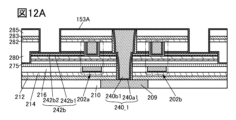
- a conductive film 153A that will become the conductor 153 is formed so as to cover the opening and the insulator 285 (FIG. 12A).
- the conductive film 153A is preferably formed in contact with the side and bottom surfaces of the opening.
- the conductive film 153A is preferably formed using a film forming method with good coverage, such as an ALD method or a CVD method.
- a film forming method with good coverage such as an ALD method or a CVD method.
- a resist mask is provided on the conductive film 153A, and the conductive film 153A is processed using a lithography method to form the conductor 153 (FIG. 12B). As a result, a portion of the conductor 153 is formed inside the opening, and another portion is in contact with a portion of the upper surface of the insulator 282.
- the conductive film 153A may be processed using a CMP method.
- the top of the conductor 153 can be shaped to roughly match the top surface of the insulator 282.
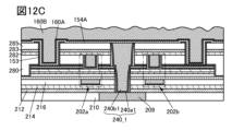
- an insulating film 154A that becomes the insulator 154 is formed on the conductor 153 (FIG. 12C).
- the insulating film 154A is preferably formed in contact with the conductor 153 provided inside the opening.
- the insulating film 154A is preferably formed using a film forming method with good coverage, such as ALD or CVD.
- the insulating film 154A is preferably formed using the above-mentioned high-k material.
- the average surface roughness of the upper surface of the conductive film 160B may become large, as shown in FIG. 12C.
- the conductor 160 in the lower layer that is, the upper electrode of the capacitor elements 101a and 101b shown in FIG. 13B
- the conductor 261 in the upper layer that is, Since the back gate electrodes of transistors 201a and 201b shown in FIG. 14 are formed
- the conductor 160 in the lower layer has the same material as the conductor 261 in the upper layer.
- the lower layer insulator 154 and the upper layer insulator 263 are formed from the insulating film 154A, the lower layer insulator 154 is made of the same material as the upper layer insulator 263.
- the manufacturing process of the semiconductor device according to this embodiment can be reduced. , productivity of the semiconductor device can be improved.
- the capacitive elements 101a and 101b can be formed.
- insulator 284 it is preferable to provide an insulator 284 and embed it between the adjacent conductors 160 and 261 (FIG. 13B). Further, it is preferable to planarize the insulator 284 using a CMP method.
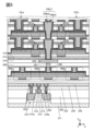
- FIG. 14 shows an example of the cross-sectional configuration at the time when the formation of the insulator 285 of the second layer 11_2 is completed.
- the conductor 261 formed in the step related to FIG. 13B is arranged to overlap the first gate electrodes of the transistors 201a and 201b, and serves as the second gate electrode of the transistors 201a and 201b. Function.
- the semiconductor device shown in FIG. 1 can be manufactured.
- the semiconductor device of this embodiment includes an OS transistor. Since an OS transistor has a small off-state current, it is possible to realize a semiconductor device or a memory device with low power consumption. Further, since the OS transistor has high frequency characteristics, it is possible to realize a semiconductor device or a memory device with high operating speed. Further, by using an OS transistor, a semiconductor device with good electrical characteristics, a semiconductor device with less variation in the electrical characteristics of transistors, a semiconductor device with a large on-state current, and a highly reliable semiconductor device or memory device can be realized.
- the conductor 240 since the conductor 240 has a stacked structure of a plurality of conductors, the manufacturing yield can be increased compared to the case where one conductor is used.
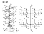
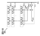
- This embodiment mode describes a configuration example of a memory device in which a layer having a functional circuit having a function of amplifying and outputting a data potential held in a memory cell is provided between layers having stacked memory cells. explain.
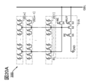
- FIG. 15 shows a block diagram of a storage device according to one embodiment of the present invention.
- the storage device 300 shown in FIG. 15 includes a drive circuit 21 and a memory array 20.
- the memory array 20 includes a plurality of memory cells 10 and a functional layer 50 having a plurality of functional circuits 51.
- FIG. 15 shows an example in which the memory array 20 has a plurality of memory cells 10 arranged in a matrix of m rows and n columns (m and n are integers of 2 or more). Further, FIG. 15 shows an example in which a functional circuit 51 is provided for each wiring BL functioning as a bit line, and the functional layer 50 includes a plurality of functional circuits 51 provided corresponding to n wirings BL. An example is shown below.
- the memory cell 10 in the first row and first column is shown as a memory cell 10[1,1] and the memory cell 10 in the mth row and nth column is shown as a memory cell 10[m,n].
- the memory cell 10 in the mth row and nth column is shown as a memory cell 10[m,n].
- i line when indicating an arbitrary line, it may be written as i line.
- column j when indicating an arbitrary column, it may be written as column j. Therefore, i is an integer of 1 or more and m or less, and j is an integer of 1 or more and n or less.
- the memory cell 10 in the i-th row and j-th column is referred to as a memory cell 10[i,j].
- the memory array 20 includes m wires WL extending in the row direction, m wires PL extending in the row direction, and n wires BL extending in the column direction.
- the wiring WL provided in the first (first row) is referred to as wiring WL[1]
- the wiring WL provided in m-th (m-th row) is referred to as wiring WL[m].
- the first wiring PL (first row) is designated as wiring PL[1]
- the mth wiring PL (mth row) is designated as wiring PL[m].
- the wiring BL provided in the first (first column) is referred to as wiring BL[1]
- the wiring BL provided in the nth (nth column) is referred to as wiring BL[n].
- the plurality of memory cells 10 provided in the i-th row are electrically connected to the i-th wiring WL (wiring WL[i]) and the i-th wiring PL (wiring PL[i]).
- the plurality of memory cells 10 provided in the j-th column are electrically connected to the j-th column wiring BL (wiring BL[j]).
- DOSRAM (registered trademark) (Dynamic Oxide Semiconductor Random Access Memory) can be applied to the memory array 20.
- DOSRAM is a RAM having 1T (transistor) 1C (capacitance) type memory cells, and refers to a memory whose access transistor is an OS transistor. The current flowing between the source and drain of the OS transistor in the off state, that is, the leakage current is extremely small.
- DOSRAM can hold charge corresponding to data held in a capacitive element (capacitor) for a long time by turning off the access transistor (making it non-conductive). Therefore, DOSRAM can reduce the frequency of refresh operations compared to DRAM configured with a transistor (Si transistor) having silicon in a channel formation region. As a result, it is possible to reduce power consumption.
- the memory cells 10 can be provided in a stacked manner.
- a plurality of memory arrays 20[1] to 20[m] can be stacked and provided.
- the memory arrays 20[1] to 20[m] included in the memory array 20 in a direction perpendicular to the surface of the substrate on which the drive circuit 21 is provided, it is possible to improve the memory density of the memory cell 10.
- the memory array 20 can be fabricated using the same manufacturing process repeatedly in the vertical direction.
- the storage device 300 can reduce the manufacturing cost of the memory array 20.
- the wiring BL functions as a bit line for writing and reading data.
- the wiring WL functions as a word line for controlling on or off (conductive state or non-conductive state) of an access transistor functioning as a switch.
- the wiring PL has a function as a constant potential line connected to the capacitive element.
- a wiring CL (not shown) can be separately provided as a wiring having a function of transmitting a backgate potential to the backgate of the OS transistor, which is an access transistor. Further, the wiring PL may also have a function of transmitting the back gate potential.
- the memory cells 10 each of the memory arrays 20[1] to 20[m] have are connected to the functional circuit 51 via the wiring BL.
- the wiring BL can be arranged in a direction perpendicular to the surface of the substrate on which the drive circuit 21 is provided.
- the length of the wiring between the memory array 20 and the functional circuit 51 can be reduced. It can be made shorter. Therefore, the signal propagation distance between two circuits connected to the bit line can be shortened, and the resistance and parasitic capacitance of the bit line can be significantly reduced, so that power consumption and signal delay can be reduced. Furthermore, it is possible to operate the memory cell 10 even if the capacitance of the capacitive element is reduced.
- the functional circuit 51 has a function of amplifying the data potential held in the memory cell 10 and outputting it to the sense amplifier 46 included in the drive circuit 21 via a wiring GBL (not shown) to be described later. With this configuration, a slight potential difference in the wiring BL can be amplified when reading data.
- the wiring GBL can be arranged in a direction perpendicular to the surface of the substrate on which the drive circuit 21 is provided. By providing the wiring BL and wiring GBL extending from the memory cells 10 of the memory arrays 20 [1] to 20 [m] in the vertical direction of the substrate surface, the wiring between the functional circuit 51 and the sense amplifier 46 can be reduced. The length can be shortened. Therefore, the signal propagation distance between the two circuits connected to the wiring GBL can be shortened, and the resistance and parasitic capacitance of the wiring GBL can be significantly reduced, so that power consumption and signal delay can be reduced.
- the wiring BL is provided in contact with the semiconductor layer of the transistor included in the memory cell 10.
- the wiring BL is provided in contact with a region functioning as a source or drain of a semiconductor layer of a transistor included in the memory cell 10.
- the wiring BL is provided in contact with a conductor provided in contact with a region functioning as a source or drain of a semiconductor layer of a transistor included in the memory cell 10.
- the wiring BL can be said to be a wiring for electrically connecting each of the sources and drains of the transistors included in the memory cells 10 in each layer of the memory array 20 and the functional circuit 51 in the vertical direction.
- the memory array 20 can be provided over the drive circuit 21. By overlapping the drive circuit 21 and the memory array 20, the signal propagation distance between the drive circuit 21 and the memory array 20 can be shortened. Therefore, the resistance and parasitic capacitance between the drive circuit 21 and the memory array 20 are reduced, and power consumption and signal delay can be reduced. Furthermore, the storage device 300 can be made smaller.
- the functional circuit 51 is constructed of OS transistors like the transistors included in the memory cell 10 of the DOSRAM, and can be freely mounted on a circuit using Si transistors in the same way as the memory arrays 20[1] to 20[m]. Since it can be arranged, integration can be easily performed. By configuring the functional circuit 51 to amplify the signal, it is possible to reduce the size of circuits such as the sense amplifier 46, which is a subsequent circuit, so that the storage device 300 can be made smaller.
- the drive circuit 21 includes a PSW 22 (power switch), a PSW 23, and a peripheral circuit 31.
- the peripheral circuit 31 includes a peripheral circuit 41, a control circuit 32, and a voltage generation circuit 33.
- each circuit, each signal, and each voltage can be removed or discarded as necessary. Alternatively, other circuits or other signals may be added.
- Signal BW, signal CE, signal GW, signal CLK, signal WAKE, signal ADDR, signal WDA, signal PON1, and signal PON2 are input signals from the outside, and signal RDA is an output signal to the outside.
- Signal CLK is a clock signal.
- the signal BW, the signal CE, and the signal GW are control signals.
- Signal CE is a chip enable signal
- signal GW is a global write enable signal
- signal BW is a byte write enable signal.
- Signal ADDR is an address signal.
- Signal WDA is write data
- signal RDA is read data.
- Signal PON1 and signal PON2 are power gating control signals. Note that the signal PON1 and the signal PON2 may be generated by the control circuit 32.
- the control circuit 32 is a logic circuit that has a function of controlling the overall operation of the storage device 300. For example, the control circuit performs a logical operation on the signal CE, the signal GW, and the signal BW to determine the operation mode (eg, write operation, read operation) of the storage device 300. Alternatively, the control circuit 32 generates a control signal for the peripheral circuit 41 so that this operation mode is executed.
- the control circuit performs a logical operation on the signal CE, the signal GW, and the signal BW to determine the operation mode (eg, write operation, read operation) of the storage device 300.
- the control circuit 32 generates a control signal for the peripheral circuit 41 so that this operation mode is executed.
- the voltage generation circuit 33 has a function of generating a negative voltage.
- the signal WAKE has a function of controlling input of the signal CLK to the voltage generation circuit 33. For example, when an H level signal is applied to the signal WAKE, the signal CLK is input to the voltage generation circuit 33, and the voltage generation circuit 33 generates a negative voltage.
- the peripheral circuit 41 is a circuit for writing and reading data to and from the memory cell 10. Further, the peripheral circuit 41 is a circuit that outputs various signals for controlling the functional circuit 51.
- the peripheral circuit 41 includes a row decoder 42, a column decoder 44, a row driver 43, a column driver 45, an input circuit 47, and an output circuit 48 ( It has an Output Cir.) and a sense amplifier 46 (Sense Amplifier).
- the input circuit 47 has a function of holding the signal WDA.
- the data held by the input circuit 47 is output to the column driver 45.
- the output data of the input circuit 47 is the data (Din) to be written into the memory cell 10.
- the data (Dout) read from the memory cell 10 by the column driver 45 is output to the output circuit 48.
- the output circuit 48 has a function of holding Dout. Further, the output circuit 48 has a function of outputting Dout to the outside of the storage device 300.
- the data output from the output circuit 48 is the signal RDA.
- the PSW 22 has a function of controlling the supply of VDD to the peripheral circuit 31.
- the PSW 23 has a function of controlling the supply of VHM to the row driver 43.
- the high power supply voltage of the storage device 300 is VDD
- the low power supply voltage is GND (ground potential).
- VHM is a high power supply voltage used to bring the word line to a high level, and is higher than VDD.
- the signal PON1 controls the on/off of the PSW22
- the signal PON2 controls the on/off of the PSW23.
- the number of power domains to which VDD is supplied is one, but it may be plural. In this case, a power switch may be provided for each power domain.
- the memory array 20 having the memory arrays 20[1] to 20[m] (m is an integer of 2 or more) and the functional layer 50 can be provided by overlapping multiple layers of the memory array 20 on the drive circuit 21. By overlapping multiple layers of memory arrays 20, the memory density of the memory cells 10 can be increased.
- FIG. 16B is a schematic diagram illustrating a configuration example of the functional circuit 51 connected to the wiring BL illustrated in FIG. 16A and the memory cells 10 included in the memory arrays 20[1] to 20[5] connected to the wiring BL. shows. Further, FIG. 16B illustrates a wiring GBL provided between the functional circuit 51 and the drive circuit 21. Note that a configuration in which a plurality of memory cells (memory cells 10) are electrically connected to one wiring BL is also referred to as a "memory string.” Note that in the drawings, the wiring GBL may be illustrated with thick lines to improve visibility.
- FIG. 16B illustrates an example of the circuit configuration of the memory cell 10 connected to the wiring BL.
- the memory cell 10 includes a transistor 11 and a capacitor 12. Regarding the transistor 11, the capacitive element 12, and each wiring (such as the wiring BL and the wiring WL), for example, the wiring BL[1] and the wiring WL[1] may be referred to as the wiring BL and the wiring WL.
- Embodiment 1 can be referred to for an example of the cross-sectional configuration of the memory cell 10 corresponding to the circuit configuration.
- the wiring BL (conductor 240) is directly connected to a conductive region including a region that functions as either the source electrode or the drain electrode of the transistor 11 (transistor 201a). It contacts at least one of the upper surface, side surface, and lower surface of the body 242a. Thereby, there is no need to provide a separate electrode for connection, so the area occupied by the memory array 20 can be reduced. Furthermore, the degree of integration of the memory cells 10 is improved, and the storage capacity of the memory device 300 can be increased.
- one of the source and drain of the transistor 11 is connected to the wiring BL.
- the other of the source and drain of the transistor 11 is connected to one electrode of the capacitive element 12.
- the other electrode of the capacitive element 12 is connected to the wiring PL.
- the gate of the transistor 11 is connected to the wiring WL.
- the back gate of the transistor 11 is connected to the wiring CL.
- the wiring PL is a wiring that provides a constant potential to maintain the potential of the capacitive element 12.
- the wiring CL is a constant potential for controlling the threshold voltage of the transistor 11.
- the wiring PL and the wiring CL may be at the same potential. In this case, by connecting two wires, the number of wires connected to the memory cell 10 can be reduced.
- FIG. 17A shows a schematic diagram of a storage device 300 in which a repeating unit 70 is a functional circuit 51 and memory arrays 20[1] to 20[m]. Note that although one wiring GBL is shown in FIG. 17A, the wiring GBL may be provided as appropriate depending on the number of functional circuits 51 provided in the functional layer 50.
- the wiring GBL is provided in contact with the semiconductor layer of the transistor included in the functional circuit 51.
- the wiring GBL is provided in contact with a region functioning as a source or drain of a semiconductor layer of a transistor included in the functional circuit 51.
- the wiring GBL is provided in contact with a conductor provided in contact with a region functioning as a source or drain of a semiconductor layer of a transistor included in the functional circuit 51.
- the wiring GBL can be said to be a wiring for electrically connecting one of the source or drain of the transistor included in the functional circuit 51 in the functional layer 50 and the drive circuit 21 in the vertical direction.
- the repeating unit 70 having the functional circuit 51 and the memory arrays 20[1] to 20[m] may be further stacked.
- the storage device 300A according to one embodiment of the present invention can have repeating units 70[1] to 70[p] (p is an integer of 2 or more) as illustrated in FIG. 17B.
- the wiring GBL is connected to the functional layer 50 that the repeating unit 70 has.
- the wiring GBL may be provided as appropriate depending on the number of functional circuits 51.
- OS transistors are provided in a stacked manner, and wiring functioning as a bit line is arranged in a direction perpendicular to the surface of the substrate on which the drive circuit 21 is provided.
- the wiring extending from the memory array 20 and functioning as a bit line in a direction perpendicular to the substrate surface the length of the wiring between the memory array 20 and the drive circuit 21 can be shortened. Therefore, the parasitic capacitance of the bit line can be significantly reduced.
- the layer in which the memory array 20 is provided includes a functional layer 50 having a functional circuit 51 having a function of amplifying and outputting the data potential held in the memory cell 10.
- FIG. 18 A configuration example of the functional circuit 51 described in FIGS. 15 to 17 and a configuration example of the sense amplifier 46 included in the memory array 20 and the drive circuit 21 will be described using FIG. 18.
- the memory cells 10 memory cell 10_A, memory cell 10_B
- the memory cells 10 connected to different wiring BL (wiring BL_A, wiring BL_B) are connected to functional circuits 51 (functional circuit 51_A, functional circuit 51_B).
- a drive circuit 21 connected to wiring GBL (wiring GBL_A, wiring GBL_B) is illustrated.
- a precharge circuit 71_A, a precharge circuit 71_B, a switch circuit 72_A, a switch circuit 72_B, and a write/read circuit 73 are illustrated.
- Transistors 52_a, 52_b, 53_a, 53_b, 54_a, 54_b, 55_a, and 55_b are illustrated as the functional circuits 51_A and 51_B.
- the transistors 52_a, 52_b, 53_a, 53_b, 54_a, 54_b, 55_a, and 55_b illustrated in FIG. 18 are OS transistors like the transistor 11 included in the memory cell 10.
- the functional layer 50 having the functional circuit 51 can be provided in a stacked manner similar to the memory arrays 20[1] to 20[m].
- the wiring BL_A is connected to the gate of the transistor 52_a, and the wiring BL_B is connected to the gate of the transistor 52_b.
- the wiring GBL_A is connected to one of the sources and drains of the transistors 53_a and 54_a.
- the wiring GBL_B is connected to one of the sources and drains of the transistors 53_b and 54_b.
- Wirings GBL_A and GBL_B are provided in the vertical direction similarly to wirings BL_A and BL_B, and are connected to transistors included in the drive circuit 21. As shown in FIG. 18, the selection signal MUX, the control signal WE, or the control signal RE is applied to the gates of the transistors 53_a, 53_b, 54_a, 54_b, 55_a, and 55_b, respectively.
- Transistors 81_1 to 81_6 and 82_1 to 82_4 that constitute the sense amplifier 46, precharge circuit 71_A, and precharge circuit 71_B shown in FIG. 18 are composed of Si transistors.
- the switches 83_A to 83_D making up the switch circuit 72_A and the switch circuit 72_B can also be made of Si transistors.
- One of the sources or drains of the transistors 53_a, 53_b, 54_a, and 54_b is connected to a transistor or a switch forming the precharge circuit 71_A, the precharge circuit 71_B, the sense amplifier 46, and the switch circuit 72_A.
- the precharge circuit 71_A includes n-channel transistors 81_1 to 81_3.
- the precharge circuit 71_A sets the wiring BL_A and the wiring BL_B to an intermediate potential between a high power supply potential (VDD) and a low power supply potential (VSS) corresponding to a potential VDD/2 according to a precharge signal applied to a precharge line PCL1. This is a circuit for precharging to potential VPC.
- the precharge circuit 71_B has n-channel transistors 81_4 to 81_6.
- the precharge circuit 71_B is a circuit for precharging the wiring GBL_A and the wiring GBL_B to an intermediate potential VPC corresponding to the potential VDD/2 between VDD and VSS in accordance with a precharge signal applied to the precharge line PCL2. be.
- the sense amplifier 46 includes p-channel transistors 82_1 and 82_2 and n-channel transistors 82_3 and 82_4, which are connected to the wiring VHH or the wiring VLL.
- the wiring VHH or the wiring VLL is a wiring that has a function of providing VDD or VSS.
- the transistors 82_1 to 82_4 are transistors forming an inverter loop.
- the potentials of the wiring GBL_A and the wiring GBL_B can be output to the outside via the switch 83_C, the switch 83_D, and the write/read circuit 73.
- the wiring BL_A and the wiring BL_B, and the wiring GBL_A and the wiring GBL_B correspond to a bit line pair.
- writing of a data signal is controlled according to the signal EN_data.
- the switch circuit 72_A is a circuit for controlling the conduction state between the sense amplifier 46 and the wiring GBL_A and the wiring GBL_B.
- the switch circuit 72_A is turned on or off under the control of the switching signal CSEL1.
- the switches 83_A and 83_B are n-channel transistors, they are turned on when the switching signal CSEL1 is at a high level, and turned off when the switching signal CSEL1 is at a low level.
- the switch circuit 72_B is a circuit for controlling the conduction state between the write/read circuit 73 and the bit line pair connected to the sense amplifier 46.
- the switch circuit 72_B is turned on or off under the control of the switching signal CSEL2.
- the switches 83_C and 83_D may be configured in the same manner as the switches 83_A and 83_B.
- the potential of the wiring WL connected to the gate of the transistor 11 of the memory cell 10 in which a data signal is to be written is set to a high level.
- the control signal WE and the signal EN_data are set to high level, and the data signal is written into the memory cell via the wiring GBL and the wiring BL.
- the GPU module 1204 has a chip 1200 using SoC technology, its size can be reduced. Furthermore, since it is excellent in image processing, it is suitable for use in portable electronic devices such as smartphones, tablet terminals, laptop PCs, and portable (portable) game machines.
- a product-sum calculation circuit using the GPU 1212 can be used to create deep neural networks (DNNs), convolutional neural networks (CNNs), recurrent neural networks (RNNs), autoencoders, deep Boltzmann machines (DBMs), and deep belief networks ( DBN), the chip 1200 can be used as an AI chip, or the GPU module 1204 can be used as an AI system module.
- DNNs deep neural networks
- CNNs convolutional neural networks
- RNNs recurrent neural networks
- DBMs deep Boltzmann machines
- DBN deep belief networks
- the electronic component 730 can be mounted on other boards using various mounting methods, not limited to BGA and PGA. Examples of implementation methods include SPGA (Staggered Pin Grid Array), LGA (Land Grid Array), QFP (Quad Flat Package), and QFJ (Quad Flat J-lead). d package) and QFN (Quad Flat Non-leaded package) can be mentioned.
- FIGS. 24A to 24J and FIGS. 25A to 25E show how the electronic component 700 or the electronic component 730 having the storage device described in the previous embodiment is included in each electronic device. Illustrated.
- An information terminal 5500 shown in FIG. 24A is a mobile phone (smartphone) that is a type of information terminal.
- the information terminal 5500 includes a housing 5510 and a display section 5511.
- the display section 5511 is equipped with a touch panel
- the housing 5510 is equipped with buttons.
- the wearable terminal can hold temporary files generated when an application is executed by applying the storage device of one embodiment of the present invention.
- FIG. 24E shows a portable game machine 5200, which is an example of a game machine.
- the portable game machine 5200 includes a housing 5201, a display portion 5202, buttons 5203, and the like.
- the storage device of one embodiment of the present invention By applying the storage device of one embodiment of the present invention to the portable game machine 5200 or the stationary game machine 7500, power consumption can be reduced. Further, by reducing power consumption, heat generation from the circuit can be reduced, and the influence of heat generation on the circuit itself, peripheral circuits, and modules can be reduced.
- a storage device can be applied to an automobile, which is a moving object, and around the driver's seat of the automobile.
- the 5700 car is equipped with an instrument panel near the driver's seat that provides a variety of information by displaying speedometer, tachometer, mileage, fuel gauge, gear status, air conditioner settings, etc. Further, a storage device showing such information may be provided around the driver's seat.
- moving body is not limited to a car.
- moving objects include trains, monorails, ships, and flying objects (helicopters, unmanned aerial vehicles (drones), airplanes, and rockets).
- FIG. 24H shows a digital camera 6240, which is an example of an imaging device.
- the digital camera 6240 includes a housing 6241, a display section 6242, an operation switch 6243, a shutter button 6244, and the like, and a detachable lens 6246 is attached to the digital camera 6240.
- the digital camera 6240 is configured here so that the lens 6246 can be removed from the housing 6241 and replaced, the lens 6246 and the housing 6241 may be integrated. Further, the digital camera 6240 may have a configuration in which a strobe device, a viewfinder, etc. can be separately attached.
- power consumption can be reduced. Further, by reducing power consumption, heat generation from the circuit can be reduced, and the influence of heat generation on the circuit itself, peripheral circuits, and modules can be reduced.
- FIG. 24I shows a video camera 6300, which is an example of an imaging device.
- the video camera 6300 includes a first housing 6301, a second housing 6302, a display portion 6303, an operation switch 6304, a lens 6305, a connecting portion 6306, and the like.
- the operation switch 6304 and the lens 6305 are provided in the first casing 6301, and the display portion 6303 is provided in the second casing 6302.
- the first casing 6301 and the second casing 6302 are connected by a connecting part 6306, and the angle between the first casing 6301 and the second casing 6302 can be changed by the connecting part 6306. be.
- the image on the display section 6303 may be switched according to the angle between the first casing 6301 and the second casing 6302 at the connection section 6306.
- a storage device can be applied to an implantable cardioverter defibrillator (ICD).
- ICD implantable cardioverter defibrillator
- the ICD main body 5400 is surgically installed in the body, and the two wires are passed through the subclavian vein 5405 and the superior vena cava 5406, and one wire tip is placed in the right ventricle and the other wire tip is placed in the right atrium. to be done.
- the ICD main body 5400 has a function as a pacemaker, and paces the heart when the heart rate is out of a specified range. In addition, if the heart rate does not improve with pacing (such as rapid ventricular tachycardia or ventricular fibrillation), electric shock treatment is performed.
- pacing such as rapid ventricular tachycardia or ventricular fibrillation
- the ICD main body 5400 needs to constantly monitor heart rate in order to appropriately perform pacing and electric shock. Therefore, ICD main body 5400 has a sensor for detecting heart rate. Further, the ICD main body 5400 can store heart rate data acquired by the sensor, the number of times pacing treatment has been performed, time, etc. in the electronic component 700.
- the ICD main body 5400 can have higher safety by having a plurality of batteries. Specifically, even if some of the batteries in the ICD main body 5400 become unusable, the remaining batteries can function, so it also functions as an auxiliary power source.
- antenna 5404 may have an antenna that can transmit physiological signals.
- a system may be configured to monitor cardiac activity.
- the expansion device 6100 includes a housing 6101, a cap 6102, a USB connector 6103, and a board 6104.
- a board 6104 is housed in a housing 6101.
- the substrate 6104 is provided with a circuit that drives a storage device or the like of one embodiment of the present invention.
- an electronic component 700 and a controller chip 6106 are attached to the board 6104.
- the USB connector 6103 functions as an interface for connecting to an external device.
- SD card A storage device according to one embodiment of the present invention can be applied to an SD card that can be attached to an electronic device such as an information terminal or a digital camera.
- FIG. 25B is a schematic diagram of the external appearance of the SD card
- FIG. 25C is a schematic diagram of the internal structure of the SD card.
- the SD card 5110 has a housing 5111, a connector 5112, and a board 5113.
- a connector 5112 functions as an interface for connecting to an external device.
- the board 5113 is housed in a housing 5111.
- the substrate 5113 is provided with a memory device and a circuit that drives the memory device.
- an electronic component 700 and a controller chip 5115 are attached to the board 5113.
- the circuit configurations of the electronic component 700 and the controller chip 5115 are not limited to those described above, and the circuit configurations may be changed as appropriate depending on the situation. For example, a write circuit, a row driver, a read circuit, etc. included in the electronic component may be incorporated into the controller chip 5115 instead of the electronic component 700.
- FIG. 25D is a schematic diagram of the external appearance of the SSD
- FIG. 25E is a schematic diagram of the internal structure of the SSD.
- the SSD 5150 includes a housing 5151, a connector 5152, and a board 5153.
- a connector 5152 functions as an interface for connecting to an external device.
- the board 5153 is housed in a housing 5151.
- the substrate 5153 is provided with a memory device and a circuit that drives the memory device.
- an electronic component 700, a memory chip 5155, and a controller chip 5156 are attached to the board 5153.
- the capacity of the SSD 5150 can be increased.
- a work memory is incorporated in the memory chip 5155.
- a DRAM chip can be used as the memory chip 5155.
- the controller chip 5156 incorporates a processor, an ECC (Error Check and Correct) circuit, and the like. Note that the circuit configurations of the electronic component 700, the memory chip 5155, and the controller chip 5115 are not limited to those described above, and the circuit configurations may be changed as appropriate depending on the situation.
- the controller chip 5156 may also be provided with a memory that functions as a work memory.
- the computer 5620 can have the configuration shown in the perspective view shown in FIG. 26B.
- a computer 5620 has a motherboard 5630, and the motherboard 5630 has a plurality of slots 5631 and a plurality of connection terminals.
- a PC card 5621 is inserted into the slot 5631.
- the PC card 5621 has a connection terminal 5623, a connection terminal 5624, and a connection terminal 5625, each of which is connected to the motherboard 5630.
- the semiconductor device 5627 has a plurality of terminals, and the semiconductor device 5627 and the board 5622 are electrically connected by, for example, reflow soldering the terminals to wiring provided on the board 5622. be able to.
- Examples of the semiconductor device 5627 include an FPGA (Field Programmable Gate Array), a GPU, and a CPU.
- an electronic component 730 can be used as the semiconductor device 5627.
- the computer 5600 can also function as a parallel computer. By using the computer 5600 as a parallel computer, for example, large-scale calculations required for artificial intelligence learning and inference can be performed.
- the electronic devices can be made smaller and have lower power consumption. Furthermore, since the storage device of one embodiment of the present invention consumes less power, heat generation from the circuit can be reduced. Therefore, the adverse effect of the heat generation on the circuit itself, peripheral circuits, and module can be reduced. Furthermore, by using the storage device of one embodiment of the present invention, an electronic device that operates stably even in a high-temperature environment can be achieved. Therefore, the reliability of electronic equipment can be improved.
- FIG. 27 shows an artificial satellite 6800 as an example of space equipment.
- the artificial satellite 6800 includes a body 6801, a solar panel 6802, an antenna 6803, a secondary battery 6805, and a control device 6807. Note that in FIG. 27, a planet 6804 is illustrated in outer space.
- outer space is an environment with more than 100 times higher radiation levels than on the ground.
- radiation include electromagnetic waves (electromagnetic radiation) represented by X-rays and gamma rays, and particle radiation represented by alpha rays, beta rays, neutron rays, proton rays, heavy ion rays, meson rays, etc. It will be done.
- the electric power necessary for the operation of the artificial satellite 6800 is generated.
- the power necessary for satellite 6800 to operate may not be generated.
- the solar panel is sometimes called a solar cell module.
- the satellite 6800 can generate signals.
- the signal is transmitted via antenna 6803 and can be received by a ground-based receiver or other satellite, for example.
- a ground-based receiver or other satellite for example.
- the position of the receiver that received the signal can be measured.
- the artificial satellite 6800 can constitute a satellite positioning system.
- control device 6807 has a function of controlling the artificial satellite 6800.
- the control device 6807 is configured using one or more selected from, for example, a CPU, a GPU, and a storage device.
- a semiconductor device including an OS transistor which is one embodiment of the present invention, is preferably used for the control device 6807.
- OS transistors Compared to Si transistors, OS transistors have smaller fluctuations in electrical characteristics due to radiation irradiation. In other words, it is highly reliable and can be suitably used even in environments where radiation may be incident.
- the artificial satellite 6800 can be configured to include a sensor.
- the artificial satellite 6800 can have a function of detecting sunlight reflected by hitting an object provided on the ground.
- the artificial satellite 6800 can have a function of detecting thermal infrared rays emitted from the earth's surface.
- the artificial satellite 6800 can have the function of, for example, an earth observation satellite.
- an artificial satellite is illustrated as an example of space equipment, but the present invention is not limited to this.
- the semiconductor device of one embodiment of the present invention can be suitably used for space equipment such as a spacecraft, a space capsule, and a space probe.
- an OS transistor can be used as a transistor constituting a semiconductor device installed in a working robot at a nuclear power plant or a radioactive waste treatment or disposal site.
- it can be suitably used for transistors constituting semiconductor devices installed in remote-controlled robots that are remotely operated for dismantling nuclear reactor facilities, removing nuclear fuel or fuel debris, and conducting field surveys of spaces with a large amount of radioactive materials.
- a base silicon oxide film, a hafnium oxide film (hereinafter referred to as HfOx film), a silicon oxide film (hereinafter referred to as SiOx film), and an In-Ga-Zn oxide film (hereinafter referred to as SiOx film) are formed on a silicon substrate.
- IGZO film laminated film of tantalum nitride and tungsten
- SiNx ⁇ SiOx film laminated film of silicon nitride and silicon oxide
- W film tungsten film
- SOC film SOC film
- SOG film SOG film
- the base silicon oxide film corresponds to the insulator 216 shown in FIGS. 8A to 8F.
- the HfOx film corresponds to the insulator 222.
- the SiOx film corresponds to the insulating film 224f and the insulator 224.
- the IGZO film corresponds to a laminated film of an oxide film 230af and an oxide film 230bf, and a laminated film of an oxide 230a and an oxide 230b.
- the TaNx ⁇ W film corresponds to a laminated film of a conductive film 242_1f and a conductive film 242_2f, and a laminated film of a conductor 242_1 and a conductor 242_2.
- the SiNx ⁇ SiOx film corresponds to the insulating film 271f and the insulator 271.
- the W film corresponds to the hard mask layer 276f and the hard mask layer 276.
- the SOC film corresponds to the organic coating film 277f and the organic coating film 277.
- the SOG film corresponds to the organic coating film 278f and the organic coating film 278.
- the etching selectivity ratio of the TaNx film to the SOC film (hereinafter referred to as the TaNx/SOC selectivity ratio) and the etching selectivity ratio of the W film to the SOC film (hereinafter referred to as the W/SOC selectivity ratio) were calculated.
- the above dry etching process was performed using a CCP etching apparatus.
- the etching conditions were as follows: CHF 3 gas 35 sccm, Cl 2 gas 15 sccm, and Ar gas 10 sccm were used as etching gases, the pressure was 0.6 Pa, the distance between the electrodes was 80 mm, the upper electrode power was 1000 W, and the substrate temperature was 60 mm. °C.
- the etching rate was measured under each condition with lower electrode power of 10 W, 25 W, 50 W, and 100 W.
- FIG. 28A The measurement results of the etching rate are shown in FIG. 28A, and the etching selectivity is shown in FIG. 28B.
- the horizontal axis represents the lower electrode power (Btm Power [W])
- the vertical axis represents the etching rate [nm/min].
- the horizontal axis represents the lower electrode power (Btm Power [W])
- the vertical axis represents the etching selectivity.
- the etching rates of the TaNx film and the W film were about the same or lower than the etching rate of the SOC film.
- the TaNx/SOC selection ratio and the W/SOC selection ratio became 1.0 or less.
- the etching rate of the TaNx film and the W film was higher than the etching rate of the SOC film.
- the TaNx/SOC selection ratio was 1.38 and the W/SOC selection ratio was 1.42.
- the lower electrode power may be at least less than 25W, preferably 10W or less.
- a silicon substrate was prepared, and a base silicon oxide film was formed on the silicon substrate using the CVD method.
- an HfOx film with a thickness of 20 nm was formed on the base silicon oxide film using the ALD method.
- the IGZO film has a stacked structure of a 10 nm thick IGZO (132) film and a 15 nm thick IGZO (111) film on the IGZO (132) film.
- the IGZO (132) film corresponds to the oxide film 230af and oxide 230a shown in FIGS. 8A to 8F.
- the IGZO (111) film corresponds to the oxide film 230bf and oxide 230b shown in FIGS. 8A to 8F.
- the film was formed by a sputtering method using a target with an atomic ratio of 1:1.2.
- the TaNx ⁇ W film is a laminated film of a 5 nm thick TaNx film and a 15 nm thick W film on the TaNx film.
- the TaNx film was formed using a tantalum target in an atmosphere containing nitrogen gas.
- the W film was formed using a tungsten target.
- the SiNx ⁇ SiOx film was a laminated film of a 5 nm thick SiNx film and a 10 nm thick SiOx film on the SiNx film.
- the SiNx film was formed using a silicon target in an atmosphere containing nitrogen gas.
- the SiOx film was formed using a silicon target in an atmosphere containing oxygen gas.
- a W film with a thickness of 15 nm was formed on the SiNx ⁇ SiOx film using a sputtering method.
- an SOC film was formed on the W film using a spin coating method.
- an SOG film was formed on the SOC film using a spin coating method.
- a negative resist film was formed on the laminated film produced as described above in the same manner as in FIG. 8A.
- the resist film was irradiated with an electron beam to form an island-shaped resist mask. Note that in Sample 1A and Sample 1B, a region where the width of the island-shaped resist mask was 30 nm and a region where the width of the island-shaped resist mask was 60 nm were formed.
- Table 1 shows the conditions for the dry etching process. Table 1 shows the interelectrode distance (Gap (mm)), top electrode power (Top Power (W)), bottom electrode power (Btm Power (W)), and pressure (Press (Pa )), gas flow rate (Gas (sccm)), and substrate temperature (Tsub (° C.)).
- the SOG film was etched under the conditions shown in Table 1, and then the SOC film was etched.
- the W film is etched under the conditions shown in Table 1 (denoted as W_1 in Table 1), the SiNx ⁇ SiOx film is etched, and the TaNx ⁇ W film is etched. I did the etching.
- the lower electrode power was set to 10 W, and in the etching of the TaNx ⁇ W film of Sample 1B, the lower electrode power was set to 25 W.
- the IGZO film was etched under the conditions shown in Table 1.
- the SiOx film was etched under the conditions shown in Table 1.
- Cross-sectional SEM images were taken of Sample 1A and Sample 1B produced as described above.
- the cross-sectional SEM images were taken using Hitachi High-Tech's "SU8030" at an accelerating voltage of 5 kV.
- the TaNx ⁇ W film was significantly retracted and the width of the structure was narrower than in sample 1A where the lower electrode power was set to 10 W. It had become.
- the TaNx ⁇ W film and the IGZO film can be processed at the same time by the method shown in FIGS. 8A to 8F, so that productivity of semiconductor devices can be improved.
- the regression of the TaNx ⁇ W film was larger in the region where the width of the structure of sample 1B was 30 nm, but the regression of the TaNx ⁇ W film was suppressed in the region where the width of the structure of sample 1A was 30 nm. Ta. Therefore, as shown in the previous embodiment, even a semiconductor device having a fine structure can be processed as designed by processing it under the conditions shown in this example.
Landscapes
- Engineering & Computer Science (AREA)
- Manufacturing & Machinery (AREA)
- Thin Film Transistor (AREA)
- Semiconductor Memories (AREA)
Priority Applications (4)
| Application Number | Priority Date | Filing Date | Title |
|---|---|---|---|
| CN202380027107.2A CN118872402A (zh) | 2022-03-25 | 2023-03-13 | 半导体装置及半导体装置的制造方法 |
| KR1020247033984A KR20240163678A (ko) | 2022-03-25 | 2023-03-13 | 반도체 장치 및 반도체 장치의 제작 방법 |
| JP2024508823A JPWO2023180859A1 (https=) | 2022-03-25 | 2023-03-13 | |
| US18/848,954 US20250212387A1 (en) | 2022-03-25 | 2023-03-13 | Semiconductor device and method for manufacturing the semiconductor device |
Applications Claiming Priority (4)
| Application Number | Priority Date | Filing Date | Title |
|---|---|---|---|
| JP2022050549 | 2022-03-25 | ||
| JP2022-050549 | 2022-03-25 | ||
| JP2022050551 | 2022-03-25 | ||
| JP2022-050551 | 2022-03-25 |
Publications (1)
| Publication Number | Publication Date |
|---|---|
| WO2023180859A1 true WO2023180859A1 (ja) | 2023-09-28 |
Family
ID=88100246
Family Applications (1)
| Application Number | Title | Priority Date | Filing Date |
|---|---|---|---|
| PCT/IB2023/052379 Ceased WO2023180859A1 (ja) | 2022-03-25 | 2023-03-13 | 半導体装置及び半導体装置の作製方法 |
Country Status (5)
| Country | Link |
|---|---|
| US (1) | US20250212387A1 (https=) |
| JP (1) | JPWO2023180859A1 (https=) |
| KR (1) | KR20240163678A (https=) |
| TW (1) | TW202347622A (https=) |
| WO (1) | WO2023180859A1 (https=) |
Families Citing this family (1)
| Publication number | Priority date | Publication date | Assignee | Title |
|---|---|---|---|---|
| TWI889314B (zh) * | 2024-04-26 | 2025-07-01 | 鴻海精密工業股份有限公司 | 記憶體裝置與其製造方法 |
Citations (5)
| Publication number | Priority date | Publication date | Assignee | Title |
|---|---|---|---|---|
| WO2018178793A1 (ja) * | 2017-03-29 | 2018-10-04 | 株式会社半導体エネルギー研究所 | 半導体装置、半導体装置の作製方法 |
| WO2019049013A1 (ja) * | 2017-09-06 | 2019-03-14 | 株式会社半導体エネルギー研究所 | 半導体装置 |
| WO2020183277A1 (ja) * | 2019-03-12 | 2020-09-17 | 株式会社半導体エネルギー研究所 | 半導体装置、及び半導体装置の作製方法 |
| WO2021009620A1 (ja) * | 2019-07-18 | 2021-01-21 | 株式会社半導体エネルギー研究所 | 半導体装置、および半導体装置の作製方法 |
| WO2021038361A1 (ja) * | 2019-08-30 | 2021-03-04 | 株式会社半導体エネルギー研究所 | 半導体装置 |
Family Cites Families (1)
| Publication number | Priority date | Publication date | Assignee | Title |
|---|---|---|---|---|
| CN114424339A (zh) | 2019-09-20 | 2022-04-29 | 株式会社半导体能源研究所 | 半导体装置及半导体装置的制造方法 |
-
2023
- 2023-03-13 US US18/848,954 patent/US20250212387A1/en active Pending
- 2023-03-13 KR KR1020247033984A patent/KR20240163678A/ko active Pending
- 2023-03-13 JP JP2024508823A patent/JPWO2023180859A1/ja active Pending
- 2023-03-13 TW TW112109137A patent/TW202347622A/zh unknown
- 2023-03-13 WO PCT/IB2023/052379 patent/WO2023180859A1/ja not_active Ceased
Patent Citations (5)
| Publication number | Priority date | Publication date | Assignee | Title |
|---|---|---|---|---|
| WO2018178793A1 (ja) * | 2017-03-29 | 2018-10-04 | 株式会社半導体エネルギー研究所 | 半導体装置、半導体装置の作製方法 |
| WO2019049013A1 (ja) * | 2017-09-06 | 2019-03-14 | 株式会社半導体エネルギー研究所 | 半導体装置 |
| WO2020183277A1 (ja) * | 2019-03-12 | 2020-09-17 | 株式会社半導体エネルギー研究所 | 半導体装置、及び半導体装置の作製方法 |
| WO2021009620A1 (ja) * | 2019-07-18 | 2021-01-21 | 株式会社半導体エネルギー研究所 | 半導体装置、および半導体装置の作製方法 |
| WO2021038361A1 (ja) * | 2019-08-30 | 2021-03-04 | 株式会社半導体エネルギー研究所 | 半導体装置 |
Also Published As
| Publication number | Publication date |
|---|---|
| TW202347622A (zh) | 2023-12-01 |
| JPWO2023180859A1 (https=) | 2023-09-28 |
| KR20240163678A (ko) | 2024-11-19 |
| US20250212387A1 (en) | 2025-06-26 |
Similar Documents
| Publication | Publication Date | Title |
|---|---|---|
| JP2024000519A (ja) | 半導体装置の作製方法 | |
| WO2023180859A1 (ja) | 半導体装置及び半導体装置の作製方法 | |
| KR20240150460A (ko) | 반도체 장치 | |
| WO2023156883A1 (ja) | 半導体装置、及び半導体装置の作製方法 | |
| WO2023152586A1 (ja) | 半導体装置、及び半導体装置の作製方法 | |
| KR20240162061A (ko) | 반도체 장치 | |
| WO2023237961A1 (ja) | 半導体装置、記憶装置、及び半導体装置の作製方法 | |
| WO2023144652A1 (ja) | 記憶装置 | |
| WO2023199181A1 (ja) | 積層体の作製方法、及び半導体装置の作製方法 | |
| KR20240149947A (ko) | 반도체 장치 | |
| WO2023175422A1 (ja) | 半導体装置 | |
| CN118872402A (zh) | 半导体装置及半导体装置的制造方法 | |
| WO2023148571A1 (ja) | 半導体装置 | |
| WO2023156869A1 (ja) | 半導体装置 | |
| CN118872401A (zh) | 半导体装置 | |
| WO2024047486A1 (ja) | 記憶装置 | |
| WO2023209486A1 (ja) | 半導体装置、及び記憶装置 | |
| WO2023144653A1 (ja) | 記憶装置 | |
| WO2024028681A1 (ja) | 半導体装置、及び記憶装置 | |
| WO2024252246A1 (ja) | 半導体装置、半導体装置の作製方法 | |
| KR20240146020A (ko) | 기억 장치 | |
| CN118749229A (zh) | 半导体装置 | |
| TW202339128A (zh) | 電子裝置、電子裝置的製造方法、半導體裝置、半導體裝置的製造方法、記憶體裝置 | |
| CN118679862A (zh) | 半导体装置及半导体装置的制造方法 | |
| WO2023166374A1 (ja) | 半導体装置、及び半導体装置の作製方法 |
Legal Events
| Date | Code | Title | Description |
|---|---|---|---|
| 121 | Ep: the epo has been informed by wipo that ep was designated in this application |
Ref document number: 23774087 Country of ref document: EP Kind code of ref document: A1 |
|
| ENP | Entry into the national phase |
Ref document number: 2024508823 Country of ref document: JP Kind code of ref document: A |
|
| WWE | Wipo information: entry into national phase |
Ref document number: 202380027107.2 Country of ref document: CN |
|
| WWE | Wipo information: entry into national phase |
Ref document number: 18848954 Country of ref document: US |
|
| ENP | Entry into the national phase |
Ref document number: 20247033984 Country of ref document: KR Kind code of ref document: A |
|
| WWE | Wipo information: entry into national phase |
Ref document number: 1020247033984 Country of ref document: KR |
|
| NENP | Non-entry into the national phase |
Ref country code: DE |
|
| 122 | Ep: pct application non-entry in european phase |
Ref document number: 23774087 Country of ref document: EP Kind code of ref document: A1 |
|
| WWP | Wipo information: published in national office |
Ref document number: 18848954 Country of ref document: US |