WO2023171583A1 - 反射型マスクブランク並びに反射型マスク及びその製造方法 - Google Patents
反射型マスクブランク並びに反射型マスク及びその製造方法 Download PDFInfo
- Publication number
- WO2023171583A1 WO2023171583A1 PCT/JP2023/008186 JP2023008186W WO2023171583A1 WO 2023171583 A1 WO2023171583 A1 WO 2023171583A1 JP 2023008186 W JP2023008186 W JP 2023008186W WO 2023171583 A1 WO2023171583 A1 WO 2023171583A1
- Authority
- WO
- WIPO (PCT)
- Prior art keywords
- film
- reflective mask
- pattern
- mask blank
- substrate
- Prior art date
Links
- 238000004519 manufacturing process Methods 0.000 title claims description 18
- 239000000758 substrate Substances 0.000 claims abstract description 108
- 238000000034 method Methods 0.000 claims description 30
- 230000001681 protective effect Effects 0.000 claims description 27
- 238000010521 absorption reaction Methods 0.000 claims description 17
- 238000000059 patterning Methods 0.000 claims description 7
- 239000010410 layer Substances 0.000 description 98
- 239000006096 absorbing agent Substances 0.000 description 59
- 239000000463 material Substances 0.000 description 29
- 239000007789 gas Substances 0.000 description 27
- MZLGASXMSKOWSE-UHFFFAOYSA-N tantalum nitride Chemical class [Ta]#N MZLGASXMSKOWSE-UHFFFAOYSA-N 0.000 description 25
- 238000005530 etching Methods 0.000 description 16
- 239000011651 chromium Substances 0.000 description 15
- 230000007547 defect Effects 0.000 description 15
- BASFCYQUMIYNBI-UHFFFAOYSA-N platinum Substances [Pt] BASFCYQUMIYNBI-UHFFFAOYSA-N 0.000 description 14
- 230000003287 optical effect Effects 0.000 description 13
- 239000010948 rhodium Substances 0.000 description 10
- 229910052707 ruthenium Inorganic materials 0.000 description 10
- 238000004088 simulation Methods 0.000 description 10
- 229910052751 metal Inorganic materials 0.000 description 8
- 239000002184 metal Substances 0.000 description 8
- 229910000629 Rh alloy Inorganic materials 0.000 description 7
- KJTLSVCANCCWHF-UHFFFAOYSA-N Ruthenium Chemical compound [Ru] KJTLSVCANCCWHF-UHFFFAOYSA-N 0.000 description 7
- 238000007689 inspection Methods 0.000 description 7
- 238000012545 processing Methods 0.000 description 7
- KDLHZDBZIXYQEI-UHFFFAOYSA-N Palladium Chemical compound [Pd] KDLHZDBZIXYQEI-UHFFFAOYSA-N 0.000 description 6
- 229910000929 Ru alloy Inorganic materials 0.000 description 5
- 230000005540 biological transmission Effects 0.000 description 5
- 229910052731 fluorine Inorganic materials 0.000 description 5
- 239000011521 glass Substances 0.000 description 5
- 229910052750 molybdenum Inorganic materials 0.000 description 5
- 229910052703 rhodium Inorganic materials 0.000 description 5
- 229910052710 silicon Inorganic materials 0.000 description 5
- 229910052715 tantalum Inorganic materials 0.000 description 5
- 239000010936 titanium Substances 0.000 description 5
- YCKRFDGAMUMZLT-UHFFFAOYSA-N Fluorine atom Chemical compound [F] YCKRFDGAMUMZLT-UHFFFAOYSA-N 0.000 description 4
- 239000000460 chlorine Substances 0.000 description 4
- 238000004140 cleaning Methods 0.000 description 4
- 239000011737 fluorine Substances 0.000 description 4
- GUVRBAGPIYLISA-UHFFFAOYSA-N tantalum atom Chemical compound [Ta] GUVRBAGPIYLISA-UHFFFAOYSA-N 0.000 description 4
- 229910052719 titanium Inorganic materials 0.000 description 4
- ZAMOUSCENKQFHK-UHFFFAOYSA-N Chlorine atom Chemical compound [Cl] ZAMOUSCENKQFHK-UHFFFAOYSA-N 0.000 description 3
- PXHVJJICTQNCMI-UHFFFAOYSA-N Nickel Chemical compound [Ni] PXHVJJICTQNCMI-UHFFFAOYSA-N 0.000 description 3
- 229910004298 SiO 2 Inorganic materials 0.000 description 3
- XUIMIQQOPSSXEZ-UHFFFAOYSA-N Silicon Chemical compound [Si] XUIMIQQOPSSXEZ-UHFFFAOYSA-N 0.000 description 3
- 229910006404 SnO 2 Inorganic materials 0.000 description 3
- 229910052801 chlorine Inorganic materials 0.000 description 3
- 238000001312 dry etching Methods 0.000 description 3
- 230000000694 effects Effects 0.000 description 3
- 238000001900 extreme ultraviolet lithography Methods 0.000 description 3
- 150000002739 metals Chemical class 0.000 description 3
- 230000007261 regionalization Effects 0.000 description 3
- 239000010703 silicon Substances 0.000 description 3
- 238000012360 testing method Methods 0.000 description 3
- 238000012546 transfer Methods 0.000 description 3
- IJGRMHOSHXDMSA-UHFFFAOYSA-N Atomic nitrogen Chemical compound N#N IJGRMHOSHXDMSA-UHFFFAOYSA-N 0.000 description 2
- ZOKXTWBITQBERF-UHFFFAOYSA-N Molybdenum Chemical compound [Mo] ZOKXTWBITQBERF-UHFFFAOYSA-N 0.000 description 2
- 229910000676 Si alloy Inorganic materials 0.000 description 2
- -1 TaSi Inorganic materials 0.000 description 2
- 229910010413 TiO 2 Inorganic materials 0.000 description 2
- RTAQQCXQSZGOHL-UHFFFAOYSA-N Titanium Chemical compound [Ti] RTAQQCXQSZGOHL-UHFFFAOYSA-N 0.000 description 2
- 239000011575 calcium Substances 0.000 description 2
- 239000010949 copper Substances 0.000 description 2
- 239000010931 gold Substances 0.000 description 2
- 239000011777 magnesium Substances 0.000 description 2
- 238000001755 magnetron sputter deposition Methods 0.000 description 2
- 239000011572 manganese Substances 0.000 description 2
- 239000011733 molybdenum Substances 0.000 description 2
- 229910052758 niobium Inorganic materials 0.000 description 2
- 150000004767 nitrides Chemical class 0.000 description 2
- 229910052757 nitrogen Inorganic materials 0.000 description 2
- 229910052763 palladium Inorganic materials 0.000 description 2
- 238000000206 photolithography Methods 0.000 description 2
- VSZWPYCFIRKVQL-UHFFFAOYSA-N selanylidenegallium;selenium Chemical compound [Se].[Se]=[Ga].[Se]=[Ga] VSZWPYCFIRKVQL-UHFFFAOYSA-N 0.000 description 2
- 239000011669 selenium Substances 0.000 description 2
- 239000004065 semiconductor Substances 0.000 description 2
- VYPSYNLAJGMNEJ-UHFFFAOYSA-N silicon dioxide Inorganic materials O=[Si]=O VYPSYNLAJGMNEJ-UHFFFAOYSA-N 0.000 description 2
- XOLBLPGZBRYERU-UHFFFAOYSA-N tin dioxide Chemical compound O=[Sn]=O XOLBLPGZBRYERU-UHFFFAOYSA-N 0.000 description 2
- 229910052726 zirconium Inorganic materials 0.000 description 2
- ZCYVEMRRCGMTRW-UHFFFAOYSA-N 7553-56-2 Chemical compound [I] ZCYVEMRRCGMTRW-UHFFFAOYSA-N 0.000 description 1
- 229910018072 Al 2 O 3 Inorganic materials 0.000 description 1
- ZOXJGFHDIHLPTG-UHFFFAOYSA-N Boron Chemical compound [B] ZOXJGFHDIHLPTG-UHFFFAOYSA-N 0.000 description 1
- WKBOTKDWSSQWDR-UHFFFAOYSA-N Bromine atom Chemical compound [Br] WKBOTKDWSSQWDR-UHFFFAOYSA-N 0.000 description 1
- OYPRJOBELJOOCE-UHFFFAOYSA-N Calcium Chemical compound [Ca] OYPRJOBELJOOCE-UHFFFAOYSA-N 0.000 description 1
- OKTJSMMVPCPJKN-UHFFFAOYSA-N Carbon Chemical compound [C] OKTJSMMVPCPJKN-UHFFFAOYSA-N 0.000 description 1
- KZBUYRJDOAKODT-UHFFFAOYSA-N Chlorine Chemical compound ClCl KZBUYRJDOAKODT-UHFFFAOYSA-N 0.000 description 1
- VYZAMTAEIAYCRO-UHFFFAOYSA-N Chromium Chemical compound [Cr] VYZAMTAEIAYCRO-UHFFFAOYSA-N 0.000 description 1
- RYGMFSIKBFXOCR-UHFFFAOYSA-N Copper Chemical compound [Cu] RYGMFSIKBFXOCR-UHFFFAOYSA-N 0.000 description 1
- MYMOFIZGZYHOMD-UHFFFAOYSA-N Dioxygen Chemical compound O=O MYMOFIZGZYHOMD-UHFFFAOYSA-N 0.000 description 1
- GYHNNYVSQQEPJS-UHFFFAOYSA-N Gallium Chemical compound [Ga] GYHNNYVSQQEPJS-UHFFFAOYSA-N 0.000 description 1
- UFHFLCQGNIYNRP-UHFFFAOYSA-N Hydrogen Chemical compound [H][H] UFHFLCQGNIYNRP-UHFFFAOYSA-N 0.000 description 1
- XEEYBQQBJWHFJM-UHFFFAOYSA-N Iron Chemical compound [Fe] XEEYBQQBJWHFJM-UHFFFAOYSA-N 0.000 description 1
- FYYHWMGAXLPEAU-UHFFFAOYSA-N Magnesium Chemical compound [Mg] FYYHWMGAXLPEAU-UHFFFAOYSA-N 0.000 description 1
- PWHULOQIROXLJO-UHFFFAOYSA-N Manganese Chemical compound [Mn] PWHULOQIROXLJO-UHFFFAOYSA-N 0.000 description 1
- BUGBHKTXTAQXES-UHFFFAOYSA-N Selenium Chemical compound [Se] BUGBHKTXTAQXES-UHFFFAOYSA-N 0.000 description 1
- 229910003902 SiCl 4 Inorganic materials 0.000 description 1
- BQCADISMDOOEFD-UHFFFAOYSA-N Silver Chemical compound [Ag] BQCADISMDOOEFD-UHFFFAOYSA-N 0.000 description 1
- 229910004535 TaBN Inorganic materials 0.000 description 1
- 229910004523 TaCo Inorganic materials 0.000 description 1
- 229910004525 TaCr Inorganic materials 0.000 description 1
- 229910004517 TaFe Inorganic materials 0.000 description 1
- 229910004162 TaHf Inorganic materials 0.000 description 1
- 229910004228 TaPd Inorganic materials 0.000 description 1
- 229910004200 TaSiN Inorganic materials 0.000 description 1
- ATJFFYVFTNAWJD-UHFFFAOYSA-N Tin Chemical compound [Sn] ATJFFYVFTNAWJD-UHFFFAOYSA-N 0.000 description 1
- 230000002378 acidificating effect Effects 0.000 description 1
- 229910052787 antimony Inorganic materials 0.000 description 1
- WATWJIUSRGPENY-UHFFFAOYSA-N antimony atom Chemical compound [Sb] WATWJIUSRGPENY-UHFFFAOYSA-N 0.000 description 1
- 239000007864 aqueous solution Substances 0.000 description 1
- 229910052785 arsenic Inorganic materials 0.000 description 1
- RQNWIZPPADIBDY-UHFFFAOYSA-N arsenic atom Chemical compound [As] RQNWIZPPADIBDY-UHFFFAOYSA-N 0.000 description 1
- QVGXLLKOCUKJST-UHFFFAOYSA-N atomic oxygen Chemical compound [O] QVGXLLKOCUKJST-UHFFFAOYSA-N 0.000 description 1
- 230000015572 biosynthetic process Effects 0.000 description 1
- 229910052797 bismuth Inorganic materials 0.000 description 1
- JCXGWMGPZLAOME-UHFFFAOYSA-N bismuth atom Chemical compound [Bi] JCXGWMGPZLAOME-UHFFFAOYSA-N 0.000 description 1
- 229910052796 boron Inorganic materials 0.000 description 1
- GDTBXPJZTBHREO-UHFFFAOYSA-N bromine Substances BrBr GDTBXPJZTBHREO-UHFFFAOYSA-N 0.000 description 1
- 229910052794 bromium Inorganic materials 0.000 description 1
- 229910052793 cadmium Inorganic materials 0.000 description 1
- BDOSMKKIYDKNTQ-UHFFFAOYSA-N cadmium atom Chemical compound [Cd] BDOSMKKIYDKNTQ-UHFFFAOYSA-N 0.000 description 1
- 229910052791 calcium Inorganic materials 0.000 description 1
- 229910052799 carbon Inorganic materials 0.000 description 1
- 229910052804 chromium Inorganic materials 0.000 description 1
- 229910017052 cobalt Inorganic materials 0.000 description 1
- 239000010941 cobalt Substances 0.000 description 1
- GUTLYIVDDKVIGB-UHFFFAOYSA-N cobalt atom Chemical compound [Co] GUTLYIVDDKVIGB-UHFFFAOYSA-N 0.000 description 1
- 230000000052 comparative effect Effects 0.000 description 1
- 229910052802 copper Inorganic materials 0.000 description 1
- 238000012937 correction Methods 0.000 description 1
- 238000013461 design Methods 0.000 description 1
- 229910001882 dioxygen Inorganic materials 0.000 description 1
- 229910052733 gallium Inorganic materials 0.000 description 1
- 229910052732 germanium Inorganic materials 0.000 description 1
- GNPVGFCGXDBREM-UHFFFAOYSA-N germanium atom Chemical compound [Ge] GNPVGFCGXDBREM-UHFFFAOYSA-N 0.000 description 1
- PCHJSUWPFVWCPO-UHFFFAOYSA-N gold Chemical compound [Au] PCHJSUWPFVWCPO-UHFFFAOYSA-N 0.000 description 1
- 229910052737 gold Inorganic materials 0.000 description 1
- 229910052735 hafnium Inorganic materials 0.000 description 1
- VBJZVLUMGGDVMO-UHFFFAOYSA-N hafnium atom Chemical compound [Hf] VBJZVLUMGGDVMO-UHFFFAOYSA-N 0.000 description 1
- 229910052736 halogen Inorganic materials 0.000 description 1
- 150000002367 halogens Chemical class 0.000 description 1
- 239000001257 hydrogen Substances 0.000 description 1
- 229910052739 hydrogen Inorganic materials 0.000 description 1
- 229910000039 hydrogen halide Inorganic materials 0.000 description 1
- 239000012433 hydrogen halide Substances 0.000 description 1
- 238000005286 illumination Methods 0.000 description 1
- 229910052738 indium Inorganic materials 0.000 description 1
- APFVFJFRJDLVQX-UHFFFAOYSA-N indium atom Chemical compound [In] APFVFJFRJDLVQX-UHFFFAOYSA-N 0.000 description 1
- 239000011630 iodine Substances 0.000 description 1
- 229910052740 iodine Inorganic materials 0.000 description 1
- 238000001659 ion-beam spectroscopy Methods 0.000 description 1
- 229910052741 iridium Inorganic materials 0.000 description 1
- GKOZUEZYRPOHIO-UHFFFAOYSA-N iridium atom Chemical compound [Ir] GKOZUEZYRPOHIO-UHFFFAOYSA-N 0.000 description 1
- 239000007788 liquid Substances 0.000 description 1
- 238000001459 lithography Methods 0.000 description 1
- 229910052749 magnesium Inorganic materials 0.000 description 1
- 229910052748 manganese Inorganic materials 0.000 description 1
- 239000012528 membrane Substances 0.000 description 1
- 238000012986 modification Methods 0.000 description 1
- 230000004048 modification Effects 0.000 description 1
- 229910052759 nickel Inorganic materials 0.000 description 1
- 229910052762 osmium Inorganic materials 0.000 description 1
- SYQBFIAQOQZEGI-UHFFFAOYSA-N osmium atom Chemical compound [Os] SYQBFIAQOQZEGI-UHFFFAOYSA-N 0.000 description 1
- 229910052760 oxygen Inorganic materials 0.000 description 1
- 239000001301 oxygen Substances 0.000 description 1
- 229910052697 platinum Inorganic materials 0.000 description 1
- 239000010453 quartz Substances 0.000 description 1
- 229910052702 rhenium Inorganic materials 0.000 description 1
- WUAPFZMCVAUBPE-UHFFFAOYSA-N rhenium atom Chemical compound [Re] WUAPFZMCVAUBPE-UHFFFAOYSA-N 0.000 description 1
- MHOVAHRLVXNVSD-UHFFFAOYSA-N rhodium atom Chemical compound [Rh] MHOVAHRLVXNVSD-UHFFFAOYSA-N 0.000 description 1
- 229910052711 selenium Inorganic materials 0.000 description 1
- 229910052709 silver Inorganic materials 0.000 description 1
- 239000004332 silver Substances 0.000 description 1
- 239000002356 single layer Substances 0.000 description 1
- 238000004544 sputter deposition Methods 0.000 description 1
- 239000000126 substance Substances 0.000 description 1
- 230000003746 surface roughness Effects 0.000 description 1
- JBQYATWDVHIOAR-UHFFFAOYSA-N tellanylidenegermanium Chemical compound [Te]=[Ge] JBQYATWDVHIOAR-UHFFFAOYSA-N 0.000 description 1
- 229910052714 tellurium Inorganic materials 0.000 description 1
- PORWMNRCUJJQNO-UHFFFAOYSA-N tellurium atom Chemical compound [Te] PORWMNRCUJJQNO-UHFFFAOYSA-N 0.000 description 1
- 229910052716 thallium Inorganic materials 0.000 description 1
- BKVIYDNLLOSFOA-UHFFFAOYSA-N thallium Chemical compound [Tl] BKVIYDNLLOSFOA-UHFFFAOYSA-N 0.000 description 1
- WFKWXMTUELFFGS-UHFFFAOYSA-N tungsten Chemical compound [W] WFKWXMTUELFFGS-UHFFFAOYSA-N 0.000 description 1
- 229910052721 tungsten Inorganic materials 0.000 description 1
- 239000010937 tungsten Substances 0.000 description 1
- 229910000500 β-quartz Inorganic materials 0.000 description 1
Images


Classifications
-
- G—PHYSICS
- G03—PHOTOGRAPHY; CINEMATOGRAPHY; ANALOGOUS TECHNIQUES USING WAVES OTHER THAN OPTICAL WAVES; ELECTROGRAPHY; HOLOGRAPHY
- G03F—PHOTOMECHANICAL PRODUCTION OF TEXTURED OR PATTERNED SURFACES, e.g. FOR PRINTING, FOR PROCESSING OF SEMICONDUCTOR DEVICES; MATERIALS THEREFOR; ORIGINALS THEREFOR; APPARATUS SPECIALLY ADAPTED THEREFOR
- G03F1/00—Originals for photomechanical production of textured or patterned surfaces, e.g., masks, photo-masks, reticles; Mask blanks or pellicles therefor; Containers specially adapted therefor; Preparation thereof
- G03F1/22—Masks or mask blanks for imaging by radiation of 100nm or shorter wavelength, e.g. X-ray masks, extreme ultraviolet [EUV] masks; Preparation thereof
- G03F1/24—Reflection masks; Preparation thereof
Definitions
- the present invention relates to a reflective mask blank, a reflective mask, and a method for manufacturing the same, and in particular to EUV, which is an original plate for manufacturing an EUV (Etreme Ultra Violet) exposure mask used in the exposure process of semiconductor manufacturing.
- EUV EUV
- the present invention relates to a reflective mask blank for lithography, a reflective mask in which a mask pattern is formed on a pattern film in the reflective mask blank for EUV lithography, and a method for manufacturing the same.
- ultraviolet light with a wavelength of 193 to 365 nm has been used as a light source for exposure equipment used in semiconductor manufacturing.
- EUV light Since EUV light is easily absorbed by many substances, it is not possible to use an exposure device with a refractive optical system. For this reason, a reflective mask is used for EUV light.
- a multilayer reflective film that reflects EUV light is formed on a substrate, and an absorber film that absorbs EUV light is patterned on the multilayer reflective film.
- a protective film (sometimes referred to as a "cap layer") is usually formed between the multilayer reflective film and the absorber film to protect the multilayer reflective film from etching when forming a mask pattern.
- a low reflection layer may be formed on the absorber film.
- a low thermal expansion glass made by adding a small amount of titanium to synthetic quartz can be used for the purpose of suppressing pattern distortion due to thermal expansion during exposure.
- a film in which molybdenum (Mo) films and silicon films are alternately laminated in about 40 periods can be used.
- a ruthenium-based material with a thickness of 1 to 5 nm may be used for the protective film.
- Ruthenium (Ru)-based materials are extremely difficult to be etched by gases that do not contain oxygen, and function as an etching stopper during mask processing.
- a tantalum-based material may be used for the absorber film.
- EUV light that enters the reflective mask from the illumination optical system of the exposure device is reflected at the apertures where no absorber film is present, and absorbed at the non-apertures where the absorber film is present, so that the mask pattern is reduced and projected by the exposure device.
- the image is transferred onto the wafer through an optical system.
- EUV light normally enters the reflective mask from a direction inclined by 6 degrees. If the thickness of the absorber film is large, shadow portions of the absorber film will appear, making it impossible to faithfully transfer the mask pattern onto the wafer. This problem becomes more pronounced as the line width of the mask pattern becomes smaller, so it is required to reduce the thickness of the absorber film.
- Patent Document 1 by forming a surface reflection-enhancing film on an absorber film that is optically designed to satisfy predetermined conditions, EUV light reflected on the surface of a pattern film that is partially etched during mask processing is disclosed. By increasing the amplitude and utilizing the interference effect with the EUV light reflected by the multilayer reflective film, the thickness of the absorber film can be made thinner and the reflectance of non-aperture areas can be kept below 2%. This makes it possible.
- the pattern film is composed of an absorber film and a surface reflection enhancement film.
- Patent Document 2 discloses a reflective mask blank including a laminated film in which a low refractive material film and a high refractive material film are alternately laminated in multiple periods as an absorber film.
- An object of the present invention is to provide a reflective mask blank, a reflective mask, and a method for manufacturing the same, which can sufficiently reduce the reflectance of the patterned film while reducing the thickness of the patterned film. More specifically, it is an object of the present invention to provide a reflective mask blank, a reflective mask, and a method for manufacturing the same, which can achieve a reflectance of 1% or less with a patterned film having a thickness of 45 nm or less.
- a pattern film has a laminated structure including a substrate, a multilayer reflective film that reflects EUV light, and a total of L layers each having a different refractive index.
- a reflective mask blank provided in this order, the inventors have discovered that the above-mentioned problem can be solved by making the pattern film satisfy the following formula (1), and have completed the present invention.
- a binary reflective mask blank comprising a substrate, a multilayer reflective film that reflects EUV light, and a pattern film in this order, the pattern film having a total of L layers each having a different refractive index.
- It has a laminated structure (L is a natural number of 2 or more), and the absorption coefficient of the i-th layer from the side opposite to the substrate in the pattern film is k i , and The thickness of the i-th layer is d i (nm), the total thickness of the pattern film is d, the exposure wavelength is ⁇ (nm), and P i is 1-exp(-2 ⁇ / ⁇ *d i k i ), a reflective mask blank that satisfies the following formula (1).
- x is an integer greater than or equal to 0.
- a reflective mask wherein the pattern film in the reflective mask blank according to any one of [1] to [9] above has a patterned pattern.
- a method for manufacturing a reflective mask comprising patterning the pattern film in the reflective mask blank according to any one of [1] to [9] above.
- the present invention it is possible to provide a reflective mask blank, a reflective mask, and a method for manufacturing the same, which can sufficiently reduce the reflectance of the patterned film while reducing the thickness of the patterned film. Since the reflective mask blank of the present invention has a simple film structure, mask processing is easy.
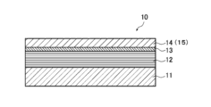
- FIG. 1 is a schematic cross-sectional view showing an example of an embodiment of a reflective mask blank of the present invention.
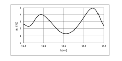
- FIG. 2 shows Example 1 in which the pattern film has a two-layer structure of a TaN film (on the substrate side: film thickness d 2 : 37.0 nm) and a Ru film (on the opposite side to the substrate: film thickness d 1 : 3.3 nm). It is a graph showing the relationship between exposure wavelength ⁇ and reflectance R for a reflective mask blank.
- FIG. 2 shows Example 1 in which the pattern film has a two-layer structure of a TaN film (on the substrate side: film thickness d 2 : 37.0 nm) and a Ru film (on the opposite side to the substrate: film thickness d 1 : 3.3 nm). It is a graph showing the relationship between exposure wavelength ⁇ and reflectance R for a reflective mask blank.
- FIG. 1 is a schematic cross-sectional view showing an example of an embodiment of a reflective mask blank of the present invention.
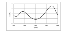
- Example 2 shows Example 2 in which the pattern film has a two-layer structure of a TaN film (on the substrate side: film thickness d 2 : 44.0 nm) and a Ru film (on the opposite side to the substrate: film thickness d 1 : 3.8 nm). It is a graph showing the relationship between exposure wavelength ⁇ and reflectance R for a reflective mask blank.
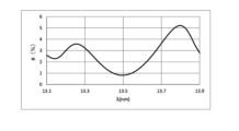
- the pattern films are a TaN film (substrate side: film thickness d 3 : 32.6 nm), a SiN film (film thickness d 2 : 2.6 nm), and a TaN film (on the side opposite to the substrate: film thickness d 1 : 4).
- FIG. 5 is a graph showing the relationship between the exposure wavelength ⁇ and the reflectance R for the reflective mask blank of Example 3 having a three-layer structure.
- FIG. 5 shows Example 4 in which the pattern film has a two-layer structure of a TaN film (on the substrate side: film thickness d 2 : 28.4 nm) and a Pt film (on the opposite side to the substrate: film thickness d 1 : 12.1 nm). It is a graph showing the relationship between exposure wavelength ⁇ and reflectance R for a reflective mask blank.
- FIG. 5 shows Example 4 in which the pattern film has a two-layer structure of a TaN film (on the substrate side: film thickness d 2 : 28.4 nm) and a Pt film (on the opposite side to the substrate: film thickness d 1 : 12.1 nm). It is a graph showing the relationship between exposure wavelength ⁇ and reflectance R for a reflective mask blank.
- FIG. 5 shows Example 4 in which the pattern film has a two-layer structure of
- Example 6 shows Example 5 in which the pattern film has a two-layer structure of a TaN film (on the substrate side: film thickness d 2 : 27.3 nm) and a Pt film (on the opposite side to the substrate: film thickness d 1 : 13.4 nm). It is a graph showing the relationship between exposure wavelength ⁇ and reflectance R for a reflective mask blank.
- FIG. 7 shows Example 6 in which the pattern film has a two-layer structure of a TaN film (on the substrate side: film thickness d 2 : 28.2 nm) and a Pt film (on the opposite side to the substrate: film thickness d 1 : 12.4 nm). It is a graph showing the relationship between exposure wavelength ⁇ and reflectance R for a reflective mask blank.
- FIG. 7 shows Example 6 in which the pattern film has a two-layer structure of a TaN film (on the substrate side: film thickness d 2 : 28.2 nm) and a Pt film (on the opposite side to the substrate: film
- Example 7 shows Example 7 in which the pattern film has a two-layer structure of a Cr film (on the substrate side: film thickness d 2 : 38.0 nm) and a Ru film (on the opposite side to the substrate: film thickness d 1 : 2.8 nm). It is a graph showing the relationship between exposure wavelength ⁇ and reflectance R for a reflective mask blank.
- the pattern films are a Cr film (substrate side: film thickness d 3 :33.1 nm), a Si film (film thickness d 2 :3.1 nm), and a Cr film (on the opposite side to the substrate: film thickness d 1 :3).
- FIG. 9 is a graph showing the relationship between the exposure wavelength ⁇ and the reflectance R for the reflective mask blank of Example 8, which has a three-layer structure with .9 nm).
- FIG. 10 shows Example 9 in which the pattern film has a two-layer structure of a SnO 2 film (on the substrate side: film thickness d 2 : 24.1 nm) and a Ru film (on the side opposite to the substrate: film thickness d 1 : 2.2 nm).
- 3 is a graph showing the relationship between the exposure wavelength ⁇ and the reflectance R for the reflective mask blank of FIG.
- any of the preferable ones can be adopted, and combinations of the preferable ones can be said to be more preferable.
- the expression "XX to YY” means “XX to YY”.
- “exp(t)” means “e t ".
- the lower and upper limits described in stages for preferred numerical ranges may be independently combined. For example, from the description "preferably 10 to 90, more preferably 30 to 60", the “preferable lower limit (10)” and “more preferable upper limit (60)” are combined to become “10 to 60". You can also do that.
- the upper limit or lower limit of the numerical range may be replaced with the value shown in the Examples.
- the reflective mask blank of this embodiment includes a substrate, a multilayer reflective film that reflects EUV light, and a pattern film in this order, and further includes other layers such as a protective film, if necessary.
- the pattern film is a layer that is partially etched during mask processing, and includes an absorber film.
- the pattern film may include a buffer layer, a low reflection layer, etc. in addition to the absorber film.
- the multilayer reflective film reflects EUV light in the openings where no absorber film is present, and the pattern film reduces the reflection of EUV light in the non-openings where the absorber film exists. It is of binary type.
- FIG. 1 is a schematic cross-sectional view showing an example of an embodiment of a reflective mask blank of the present invention.
- a multilayer reflective film 12, a protective film 13, and an absorber film 14 as a pattern film 15 are formed on a substrate 11 in this order.
- the substrate 11 satisfies the characteristics as a substrate for an EUV mask blank. Therefore, the substrate 11 has a low coefficient of thermal expansion (specifically, a coefficient of thermal expansion at 20°C of preferably 0 ⁇ 0.05 ⁇ 10 ⁇ 7 /°C, more preferably 0 ⁇ 0.03 ⁇ 10 ⁇ 7 /°C). °C), and has excellent smoothness, flatness, and resistance to cleaning liquids used for cleaning mask blanks or photomasks after pattern formation.
- the substrate 11 is made of glass having a low coefficient of thermal expansion, such as SiO 2 -TiO 2 glass, but is not limited to this, and may be made of crystallized glass with ⁇ -quartz solid solution precipitated, quartz glass, silicon, etc. A substrate made of metal or the like can also be used.
- the substrate 11 has a smooth surface with a surface roughness (rms) of 0.15 nm or less and a flatness of 100 nm or less because high reflectance and transfer accuracy can be obtained in the photomask after pattern formation.
- rms surface roughness
- the size, thickness, etc. of the substrate 11 are appropriately determined based on the design values of the mask, etc. It is preferable that there be no defects on the surface of the substrate 11 on which the multilayer reflective film 12 is formed. However, even if a defect exists, it is sufficient that no phase defect occurs due to a concave defect and/or a convex defect. Specifically, it is preferable that the depth of the concave defect and the height of the convex defect be 2 nm or less, and that the half width of the concave defect and the convex defect be 60 nm or less.
- the half-width of a concave defect refers to the width at 1/2 the depth of the concave defect.
- the half-width of a convex defect refers to the width at a position half the height of the convex defect.
- the multilayer reflective film 12 reflects EUV light and achieves high EUV light reflectance by alternately stacking high refractive index layers and low refractive index layers multiple times.
- Mo is widely used for the high refractive index layer
- Si is widely used for the low refractive index layer. That is, Mo/Si multilayer reflective film is the most common.
- the multilayer reflective film 12 is not particularly limited as long as it has the desired characteristics as a reflective layer of a reflective mask blank.
- the characteristic particularly required of the multilayer reflective film 12 is high EUV light reflectance.
- the peak reflectance of the light in the EUV wavelength region i.e., the light reflectance around the wavelength of 13.5 nm
- peak reflectance of EUV light is preferably 60% or more, more preferably 65% or more.
- the peak reflectance of EUV light is preferably 60% or more, more preferably 65% or more.
- each layer constituting the multilayer reflective film 12 and the number of repeating units of the layers can be appropriately selected depending on the film material used and the EUV light reflectance required of the reflective layer.
- the multilayer reflective film in order to make the multilayer reflective film 12 with a maximum value of EUV light reflectance of 60% or more, the multilayer reflective film should be made of Mo with a film thickness of 2.3 nm ⁇ 0.1 nm.
- This layer and a Si layer having a film thickness of 4.5 nm ⁇ 0.1 nm may be laminated so that the number of repeating units is 30 to 60.
- the thickness of the multilayer reflective film 12 can be measured, for example, using a transmission electron microscope (TEM) on a cross section taken along the thickness direction (Z direction) of the reflective mask blank.
- TEM transmission electron microscope
- the uppermost layer of the multilayer reflective film 12 is preferably made of a material that is not easily oxidized.
- the layer of material that is not easily oxidized functions as a cap layer for the multilayer reflective film 12.
- a specific example of a layer of oxidizable material that functions as a cap layer is a Si layer.
- the uppermost layer functions as a cap layer by making the uppermost layer a Si layer.
- the thickness of the cap layer is preferably 11 ⁇ 2 nm.
- the thickness of the cap layer can be measured, for example, using a transmission electron microscope (TEM) on a cross section taken along the thickness direction (Z direction) of the reflective mask blank.
- TEM transmission electron microscope
- the protective film 13 is provided for the purpose of protecting the multilayer reflective film 12 so that the multilayer reflective film 12 is not damaged by the etching process when the absorber film 14 is patterned by an etching process, usually a dry etching process. Any layer. Therefore, as the material for the protective film 13, a material is selected that is not easily affected by the etching process of the absorber film 14, that is, its etching rate is slower than that of the absorber film 14, and it is also less likely to be damaged by this etching process. . In order to satisfy the above characteristics, the protective film 13 preferably contains at least one of Rh and Ru (Ru alloy, Rh alloy, etc.).
- the above-mentioned materials include Ru metal alone, Ru alloy containing Ru and one or more metals selected from the group consisting of Si, Ti, Nb, Mo, Rh, and Zr, and Rh metal alone, Rh alloy containing Rh and one or more metals selected from the group consisting of Si, Ti, Nb, Mo, Ru, Ta, and Zr, Rh containing containing the above Rh alloy and N
- Rh-based materials such as nitrides and Rh-containing oxynitrides containing the Rh alloy, N, and O.
- examples of materials that can achieve the above object include Al, nitrides containing these metals and N, and Al 2 O 3 .
- materials that can achieve the above object are preferably Ru metal alone, Ru alloy, Rh metal alone, or Rh alloy.
- the Ru alloy is preferably a Ru--Si alloy or a Ru--Rh alloy
- the Rh alloy is preferably a Rh--Si alloy or a Rh--Ru alloy.
- the thickness of the protective film 13 is preferably 1 to 10 nm, more preferably 1 to 5 nm.
- the thickness of the protective film 13 can be measured, for example, using a transmission electron microscope (TEM) on a cross section taken along the thickness direction (Z direction) of the reflective mask blank.
- TEM transmission electron microscope
- the protective film may be a film consisting of a single layer or a multilayer film consisting of multiple layers.
- each layer constituting the multilayer film is preferably made of the above-mentioned preferred material.
- the protective film is a multilayer film, it is also preferable that the total film thickness of the multilayer film falls within the above-mentioned preferable range.
- the protective film can be formed using a known film forming method such as a magnetron sputtering method or an ion beam sputtering method.
- a known film forming method such as a magnetron sputtering method or an ion beam sputtering method.
- an Ru target as a target and Ar gas as a sputtering gas.
- a particularly required characteristic of the binary absorber film 14 is extremely low EUV light reflectance.
- the peak reflectance of EUV light when the surface of the absorber film 14 is irradiated with light in the wavelength range of EUV light is preferably 1.3% or less, more preferably 1% or less. , more preferably 0.98% or less, particularly preferably 0.50% or less, most preferably 0.30% or less.
- the reflectance of the absorber film 14 can be measured using, for example, an EUV reflectance meter.
- the absorber film 14 is made of a material with a high absorption coefficient for EUV light.
- a material containing tantalum (Ta) as a main component is preferable.
- a material containing tantalum (Ta) as a main component means a material containing 20 at% or more of Ta.
- Materials containing Ta as a main component used for the absorber film 14 include, in addition to Ta, hafnium (Hf), Si, zirconium (Zr), germanium (Ge), boron (B), palladium (Pd), tin (Sn), Chromium (Cr), manganese (Mn), iron (Fe), cobalt (Co), silver (Ag), cadmium (Cd), indium (In), antimony (Sb), tungsten (W), rhenium (Re), Osmium (Os), iridium (Ir), platinum (Pt), gold (Au), thallium (Tl), lead (Pb), bismuth (Bi), carbon (C), titanium (Ti), zirconium (Zr), Mo, Ru, rhodium (Rh), palladium (Pd), calcium (Ca), magnesium (Mg), Al, nickel (Ni), copper (Cu), zinc (Zn), gallium (Ga), arsenic (As) ,
- materials containing the above elements other than Ta include, for example, TaN, TaNH, TaHf, TaHfN, TaBSi, TaBSiN, TaB, TaBN, TaSi, TaSiN, TaGe, TaGeN, TaZr, TaZrN, TaPd, TaSn, TaPdN. , TaSn, TaCr, TaMn, TaFe, TaCo, TaAg, TaCd, TaIn, TaSb, TaW, and the like.
- the thickness of the absorber film 14 is preferably 20 to 90 nm.
- the thickness of the absorber film 14 can be measured, for example, using a transmission electron microscope (TEM) on a cross section taken along the thickness direction (Z direction) of the reflective mask blank.
- TEM transmission electron microscope
- the pattern film including the above-mentioned absorber film has a laminated structure having a total of L layers (where L is a natural number of 2 or more) having different refractive indexes.
- L is not particularly limited as long as it is a natural number of 2 or more, but is preferably 8 or less, more preferably 6 or less, and even more preferably 5 or less. That is, L is, for example, 2 to 8.
- Examples of patterned films include "a two-layer structure of a TaN film (on the substrate side) and a Pt film (on the opposite side to the substrate)" and "a two-layer structure of a Cr film (on the substrate side) and a Ru film (on the opposite side to the substrate)".
- the refractive index of the i-th layer (i is a natural number) from the side opposite to the substrate in the pattern film is n i
- the refractive index of the i-th layer from the side opposite to the substrate in the pattern film is n i.
- the absorption coefficient is k i , the thickness of the i-th layer from the side opposite to the substrate in the pattern film is di (nm), the total thickness of the pattern film is d, the exposure wavelength is ⁇ (nm),
- P i is 1-exp (-2 ⁇ / ⁇ *d i k i )
- the following formula (1) is satisfied and the following formula (1-1) is satisfied, and the following formula (1-2) is It is more preferable to satisfy.
- the refractive index n i and the absorption coefficient k i are values at a wavelength of 13.5 nm, for example.
- the reflection amplitude of the i-th layer from the side opposite to the substrate in the patterned film is r i
- the following formula (2 -1) is more preferable, and it is particularly preferable to satisfy the following formula (2-2).
- the reflection amplitude r L of the L-th layer from the side opposite to the substrate in the pattern film is calculated as
- the refractive index n1 of the first outermost layer from the side opposite to the substrate in the pattern film is not particularly limited, but from the viewpoint of generating reflection amplitude at the interface with vacuum, it is preferably 0.950 or less, more preferably is 0.945 or less, particularly preferably 0.940 or less, and is preferably 0.830 or more, more preferably from the viewpoint of utilizing the cancellation of reflected waves due to the reflection amplitude between the outermost layer and the second layer material. is 0.860 or more, particularly preferably 0.870 or more.
- the refractive index n 1 and film thickness d 1 of the first outermost layer from the side opposite to the substrate in the pattern film satisfy the following formula (3), and more preferably satisfy the following formula (3-1). , it is particularly preferable that formula (3-2) be satisfied.
- x is an integer of 0 or more.
- between the absorption coefficients k of two adjacent layers in the pattern film is preferably 0.0200 from the viewpoint of utilizing the cancellation of reflected waves.
- the above value is more preferably 0.0210 or more, particularly preferably 0.0220 or more.
- is preferably 0.0700 or less, more preferably 0.0600 or less, particularly preferably 0.0550 or less.
- the reflectance of the pattern film is not particularly limited as long as it is sufficiently reduced, but it is preferably 1.3% or less, more preferably 1% or less, and still more preferably 0.98% or less. It is particularly preferably 0.50% or less, most preferably 0.30% or less. Note that the reflectance of the patterned film can be measured with an EUV reflectance meter, and an optical multilayer film simulation can be performed.
- the total thickness d of the pattern film is not particularly limited as long as it is sufficiently reduced, but is preferably 45 nm or less, more preferably 43 nm or less, still more preferably 42 nm or less, and particularly preferably It is 41 nm or less.
- the total film thickness of the pattern film can be measured, for example, using a transmission electron microscope (TEM) on a cross section taken along the thickness direction (Z direction) of the reflective mask blank.
- TEM transmission electron microscope
- a buffer layer may be formed between the protective film 13 and the absorber film 14.
- the buffer layer is a layer that protects the multilayer reflective film during dry etching and defect correction.
- the material for the buffer layer is not particularly limited, and examples thereof include SiO 2 , CrN, and the like.
- a low reflective layer may be formed on the absorber film 14.
- the low-reflection layer is composed of a film that exhibits low reflection in the inspection light used to inspect the mask pattern.
- a pattern is formed on the absorber film and then inspected to see if the pattern is formed as designed.
- an inspection machine that uses light of approximately 193 nm or 257 nm as inspection light is used.
- the difference in the reflectance of light of about 193 nm and 257 nm, specifically, the difference between the exposed surface of the absorber film removed by patterning and the surface of the absorber film that remained without being removed by patterning.
- the former is the surface of the protective film. Therefore, if the difference in reflectance between the surface of the protective film and the surface of the absorber film with respect to the wavelength of the test light is small, the contrast during the test will be poor and accurate testing will not be possible. If the difference in reflectance between the protective film surface and the absorber film surface with respect to the wavelength of the inspection light is small, the contrast during inspection will be good due to the formation of the low reflection layer.
- the material for the low reflection layer is not particularly limited, and examples include tantalum oxynitride. Since the low reflection layer corresponds to the first outermost layer from the side opposite to the substrate in the patterned film, it is preferable that formula (3) is satisfied.
- the reflective mask of this embodiment has a pattern obtained by patterning the pattern film in the reflective mask blank of the present invention. That is, the reflective mask of this embodiment includes, in this order, a substrate, a multilayer reflective film that reflects EUV light, and a pattern in which the patterned film is patterned, and, if necessary, other layers such as a protective film. Be prepared for more. Layers other than the pattern (other layers such as the substrate, multilayer reflective film, and protective film) are as described for the reflective mask blank. The pattern will be explained in "Method for manufacturing reflective mask" below.
- a pattern film in the reflective mask blank of this embodiment is patterned. That is, the reflective mask of this embodiment can be manufactured using the reflective mask blank of this embodiment described above.
- a photolithography method that can perform high-definition patterning is most suitable.
- a resist film (not shown) is formed on the outermost surface of the reflective mask blank 10 shown in FIG. 1 (the absorber film 14 which is the uppermost layer of the pattern film 15).
- the thickness of the resist film can be, for example, 100 nm.
- a desired pattern is drawn (exposed) on this resist film, and further developed and rinsed to form a predetermined resist pattern (not shown).
- the pattern film 15 (absorber film 14) is dry etched using an etching gas containing a fluorine gas such as SF 6 using a resist pattern (not shown) as a mask. form). After pattern formation, the resist pattern (not shown) is removed.
- the etching rate of the pattern film 15 depends on the material forming the pattern film 15 (absorber film 14) and conditions such as the etching gas. Since the pattern film 15 (absorber film 14) is composed of a multilayer film made of different materials, conditions such as etching rate and etching gas may change for each layer of different materials.
- a pattern is formed by the above. If the pattern film 15 (absorber film 14) made of a multilayer film can be continuously etched by dry etching using one type of etching gas, the effect of process simplification can be obtained. Next, wet cleaning is performed using an acidic or alkaline aqueous solution to obtain a reflective mask for EUV lithography that achieves high reflectance.
- etching gases include CHF 3 , CF 4 , C 2 F 6 , C 3 F 6 , C 4 F 6 , C 4 F 8 , CH 2 F 2 , CH 3 F, and C 3 F.
- a fluorine-based gas such as 8 and F, and a mixed gas containing these fluorine gases and O 2 in a predetermined ratio can be used.
- other gases may be used as long as they are useful for processing.
- gases include, for example, chlorine-based gases such as Cl 2 , SiCl 4 , CHCl 3 , CCl 4 , BCl 3 and mixed gases thereof, mixed gases containing chlorine-based gas and He in a predetermined ratio, and chlorine-based gases. and a mixed gas containing Ar in a predetermined proportion, a halogen gas containing at least one selected from fluorine gas, chlorine gas, bromine gas, and iodine gas, and at least one type selected from the group consisting of hydrogen halide gas, or There are many more. Further examples include mixed gases containing these gases and oxygen gas.
- a binary reflective mask blank comprising a substrate, a multilayer reflective film that reflects EUV light, and a pattern film in this order, the pattern film having a total of L layers each having a different refractive index.
- It has a laminated structure (L is a natural number of 2 or more), and the absorption coefficient of the i-th layer from the side opposite to the substrate in the pattern film is k i , and The thickness of the i-th layer is d i (nm), the total thickness of the pattern film is d, the exposure wavelength is ⁇ (nm), and P i is 1-exp(-2 ⁇ / ⁇ *d i k i ), a reflective mask blank that satisfies the following formula (1).
- ⁇ 3> The reflective mask blank according to ⁇ 1> or ⁇ 2> above, wherein the first outermost layer of the patterned film from the side opposite to the substrate has a refractive index n 1 of 0.950 or less.
- n 1 refractive index
- ⁇ 4> The reflective mask according to any one of ⁇ 1> to ⁇ 3> above, wherein at least one of the differences
- ⁇ 5> The refractive index of the i-th layer from the side opposite to the substrate in the pattern film is n i , and the film thickness d 1 of the first outermost layer from the side opposite to the substrate in the pattern film is expressed by the following formula:
- x is an integer greater than or equal to 0.
- ⁇ 6> The reflective mask blank according to any one of ⁇ 1> to ⁇ 5> above, wherein the pattern film has a reflectance of 1.3% or less.
- ⁇ 7> The reflective mask blank according to any one of ⁇ 1> to ⁇ 6> above, wherein the pattern film has a reflectance of 1% or less.
- ⁇ 8> The reflective mask blank according to any one of ⁇ 1> to ⁇ 7> above, wherein the total film thickness d of the pattern film is 45 nm or less.
- ⁇ 9> The reflective mask blank according to any one of ⁇ 1> to ⁇ 8> above, further comprising a protective film between the multilayer reflective film and the pattern film.
- a reflective mask wherein the pattern film in the reflective mask blank according to any one of ⁇ 1> to ⁇ 9> above has a patterned pattern.
- ⁇ 11> A method for manufacturing a reflective mask, comprising patterning the pattern film in the reflective mask blank according to any one of ⁇ 1> to ⁇ 9> above.
- Examples 1 to 3 are comparative examples, and Examples 4 to 9 are examples.
- the reflective mask blank of Example 1 includes a substrate, a multilayer reflective film formed on the substrate, a protective film formed on the multilayer reflective film, and an absorber film as a pattern film formed on the protective film. Equipped with A SiO 2 -TiO 2 glass substrate (thickness: 6.3 mm) was selected as the substrate, and a silicon film (thickness: 4.5 nm) and a molybdenum film (thickness: 2.3 nm) were alternately repeated in the number of units.
- a laminated structure in which (thickness d 2 : 37.0 nm) and a ruthenium (Ru) film (thickness d 1 : 3.3 nm), a patterned film (absorber film) (patterned film thickness d :40.3nm).
- the absorber film on the substrate side is a tantalum nitride (TaN) film
- the absorber film on the opposite side to the substrate is a ruthenium (Ru) film.
- the left side of equation (1) 0.0109
- the left side of equation (2) 0.094
- Example 2 shows Example 1 in which the pattern film has a two-layer structure of a TaN film (on the substrate side: film thickness d 2 : 37.0 nm) and a Ru film (on the opposite side to the substrate: film thickness d 1 : 3.3 nm). It is a graph showing the relationship between exposure wavelength ⁇ and reflectance R for a reflective mask blank. The reflectance of the patterned film at a wavelength of 13.5 nm was 2.62% (Table 1). FIG. 2 was obtained by performing an optical multilayer film simulation.
- Example 2 In Example 1, a patterned film (absorbing Instead of selecting a tantalum nitride (TaN) film (film thickness d 2 : 44.0 nm) and a ruthenium (Ru) film (film thickness d 1 :3) (pattern film thickness d: 40.3 nm).
- the left side of equation (2) 0.094
- FIG. 1 a patterned film (absorbing Instead of selecting a tantalum nitride (TaN) film (film thickness d 2 : 44.0 nm) and a ruthenium (Ru) film (film thickness d 1 :3) (pattern film thickness
- Example 3 shows Example 2 in which the pattern film has a two-layer structure of a TaN film (on the substrate side: film thickness d 2 : 44.0 nm) and a Ru film (on the opposite side to the substrate: film thickness d 1 : 3.8 nm). It is a graph showing the relationship between exposure wavelength ⁇ and reflectance R for a reflective mask blank. The reflectance of the patterned film at a wavelength of 13.5 nm was 1.36% (Table 1). FIG. 3 was obtained by performing an optical multilayer film simulation.
- the pattern films are a TaN film (substrate side: film thickness d 3 : 32.6 nm), a SiN film (film thickness d 2 : 2.6 nm), and a TaN film (on the side opposite to the substrate: film thickness d 1 : 4).
- FIG. 5 nm is a graph showing the relationship between the exposure wavelength ⁇ and the reflectance R for the reflective mask blank of Example 3 having a three-layer structure.
- the reflectance of the patterned film at a wavelength of 13.5 nm was 4.01% (Table 1).
- FIG. 4 was obtained by performing an optical multilayer film simulation.
- FIG. 5 shows Example 4 in which the pattern film has a two-layer structure of a TaN film (on the substrate side: film thickness d 2 : 28.4 nm) and a Pt film (on the opposite side to the substrate: film thickness d 1 : 12.1 nm). It is a graph showing the relationship between exposure wavelength ⁇ and reflectance R for a reflective mask blank. The reflectance of the patterned film at a wavelength of 13.5 nm was 0.84% (Table 1). FIG. 5 was obtained by performing an optical multilayer film simulation.
- Example 5 shows Example 5 in which the pattern film has a two-layer structure of a TaN film (on the substrate side: film thickness d 2 : 27.3 nm) and a Pt film (on the opposite side to the substrate: film thickness d 1 : 13.4 nm). It is a graph showing the relationship between exposure wavelength ⁇ and reflectance R for a reflective mask blank. The reflectance of the patterned film at a wavelength of 13.5 nm was 0.94% (Table 1). FIG. 6 was obtained by performing an optical multilayer film simulation.
- Example 7 shows Example 6 in which the pattern film has a two-layer structure of a TaN film (on the substrate side: film thickness d 2 : 28.2 nm) and a Pt film (on the opposite side to the substrate: film thickness d 1 : 12.4 nm). It is a graph showing the relationship between exposure wavelength ⁇ and reflectance R for a reflective mask blank. The reflectance of the patterned film at a wavelength of 13.5 nm was 0.85% (Table 1). FIG. 7 was obtained by performing an optical multilayer film simulation.
- FIG. 8 shows a reflective type of Example 7 in which the pattern film has a two-layer structure of a Cr film (on the substrate side: film thickness d 2 : 38 nm) and a Ru film (on the opposite side to the substrate: film thickness d 1 : 2.8 nm). It is a graph showing the relationship between exposure wavelength ⁇ and reflectance R for a mask blank. The reflectance of the patterned film at a wavelength of 13.5 nm was 0.95% (Table 1). FIG. 8 was obtained by performing an optical multilayer film simulation.
- the pattern films are a Cr film (substrate side: film thickness d 3 :33.1 nm), a Si film (film thickness d 2 :3.1 nm), and a Cr film (on the opposite side to the substrate: film thickness d 1 :3).
- 9 is a graph showing the relationship between the exposure wavelength ⁇ and the reflectance R for the reflective mask blank of Example 8, which has a three-layer structure with .9 nm). The reflectance of the patterned film at a wavelength of 13.5 nm was 0.82% (Table 1).
- FIG. 9 was obtained by performing an optical multilayer film simulation.
- Example 10 shows Example 9 in which the pattern film has a two-layer structure of a SnO 2 film (on the substrate side: film thickness d 2 : 24.1 nm) and a Ru film (on the opposite side to the substrate: film thickness d 1 : 2.8 nm).
- FIG. 3 is a graph showing the relationship between the exposure wavelength ⁇ and the reflectance R for the reflective mask blank of FIG.
- the reflectance of the patterned film at a wavelength of 13.5 nm was 0.29% (Table 1).
- FIG. 10 was obtained by performing an optical multilayer film simulation.
- the reflective mask blanks (Examples 4 to 9) that satisfy formula (1) can sufficiently reduce the reflectance of the pattern film while reducing the thickness of the pattern film (reflectance: 0.29
- reflective mask blanks that do not satisfy formula (1) (Examples 1 to 3) cannot sufficiently reduce the reflectance of the pattern film (reflectance: 1.36 to 4). .01%).
Landscapes
- Physics & Mathematics (AREA)
- General Physics & Mathematics (AREA)
- Preparing Plates And Mask In Photomechanical Process (AREA)
- Exposure Of Semiconductors, Excluding Electron Or Ion Beam Exposure (AREA)
Abstract
基板と、EUV光を反射する多層反射膜と、パターン膜とをこの順に備えるバイナリ型の反射型マスクブランクであって、前記パターン膜は、屈折率がそれぞれ異なる層を合計L層有する積層構造であり、下記式(1)を満たす(なお、L、P、i、dは明細書中に定義されている)、反射型マスクブランクに関する。
Description
本発明は、反射型マスクブランク並びに反射型マスク及びその製造方法に関し、特に、半導体製造の露光プロセスで使用されるEUV(Etreme Ultra Violet:極端紫外)露光用マスクを製造するための原板であるEUVリソグラフィ用反射型マスクブランク、並びに、該EUVリソグラフィ用反射型マスクブランクにおけるパターン膜にマスクパターンを形成してなる反射型マスク及びその製造方法に関する。
従来、半導体製造で使用される露光装置の光源には、波長193~365nmの紫外光が用いられている。波長が短いほど露光装置の解像度は高くなる。そこで、次世代の露光装置の光源として、中心波長13.5nmのEUV光が有望視されている。
EUV光は、多くの物質に対し吸収されやすいので、屈折光学系の露光装置を用いることができない。このため、EUV光では反射型マスクが用いられている。
このような反射型マスクは、基板上にEUV光を反射する多層反射膜が形成され、多層反射膜上にEUV光を吸収する吸収体膜がパターニングされている。多層反射膜と吸収体膜の間には、通常、マスクパターンを形成する際のエッチングから多層反射膜を保護するための保護膜(「キャップ層」ということもある)が形成されている。さらに、マスク加工後のパターン欠陥検査を容易にするため、吸収体膜の上に低反射層が形成されることもある。
基板としては、露光時の熱膨張によるパターン歪を抑制する目的で合成石英に少量のチタンを添加した低熱膨張ガラスが用いられ得る。多層反射膜としては、モリブデン(Mo)膜とシリコン膜を交互に40周期程度積層した膜が用いられ得る。保護膜には厚さ1~5nmのルテニウム系材料が用いられ得る。ルテニウム(Ru)系材料は酸素を含まないガスに対し非常にエッチングされにくく、マスク加工時のエッチングストッパとして機能する。吸収体膜にはタンタル系材料が用いられ得る。
露光装置の照明光学系より反射型マスクに入射したEUV光は、吸収体膜が存在しない開口部では反射され、吸収体膜が存在する非開口部では吸収され、マスクパターンが露光装置の縮小投影光学系を通してウエハ上に転写される。反射型マスクにEUV光は通常6度傾斜した方向から入射する。吸収体膜の膜厚が厚いと、吸収体膜の影となる部分が生じ、ウエハ上に忠実にマスクパターンを転写できなくなる。この問題は、マスクパターンの線幅が小さくなるほど顕著となるため、吸収体膜の膜厚をより薄くすることが求められている。
また、バイナリ型マスクの場合、EUV露光において高精度のパターン転写を行うためには、非開口部の反射率を2%以下に抑える必要がある。
特許文献1では、所定の条件を満たすように光学設計された表面反射増強膜を吸収体膜上に形成することで、マスク加工時に部分的にエッチングされるパターン膜の表面で反射されるEUV光の振幅を大きくして、多層反射膜で反射されるEUV光との干渉効果を利用することにより、吸収体膜の膜厚をより薄くしつつ、非開口部の反射率を2%以下に抑えることを可能としている。なお、パターン膜は、吸収体膜と表面反射増強膜とで構成されている。
また、特許文献2では、吸収体膜として、低屈折材料膜と高屈折材料膜を交互に複数周期積層した積層膜を備えた反射型マスクブランクが開示されている。
特許文献1では、所定の条件を満たすように光学設計された表面反射増強膜を吸収体膜上に形成することで、マスク加工時に部分的にエッチングされるパターン膜の表面で反射されるEUV光の振幅を大きくして、多層反射膜で反射されるEUV光との干渉効果を利用することにより、吸収体膜の膜厚をより薄くしつつ、非開口部の反射率を2%以下に抑えることを可能としている。なお、パターン膜は、吸収体膜と表面反射増強膜とで構成されている。
また、特許文献2では、吸収体膜として、低屈折材料膜と高屈折材料膜を交互に複数周期積層した積層膜を備えた反射型マスクブランクが開示されている。
しかしながら、一般的に、反射型マスクブランクにおけるパターン膜の積層構造における隣接する層間の屈折率差Δnの絶対値は小さいので、パターン膜の積層構造の界面で反射されるEUV光の振幅(振幅)は、多層反射膜からの反射光の振幅(強度)よりも格段に小さい。よって、パターン膜の積層構造の界面で反射されるEUV光を用いて多層反射膜からの反射光を打ち消すという干渉効果を利用することのみによっては、EUV光の反射率がより低減された膜厚が薄いパターン膜を実現するには限界があった。
また、特許文献2において、マスク加工のために吸収体膜である積層膜をエッチングあるいは洗浄する際、積層膜の側壁にダメージが生じる問題があった。
また、特許文献2において、マスク加工のために吸収体膜である積層膜をエッチングあるいは洗浄する際、積層膜の側壁にダメージが生じる問題があった。
本発明の目的は、パターン膜の膜厚を薄くしつつ、パターン膜の反射率を十分に低減できる、反射型マスクブランク並びに反射型マスク及びその製造方法を提供することである。より具体的には、45nm以下の膜厚のパターン膜で1%以下の反射率を実現できる反射型マスクブランク並びに反射型マスク及びその製造方法を提供することである。
本発明者らは、上記課題を解決するために鋭意検討を行った結果、基板と、EUV光を反射する多層反射膜と、屈折率がそれぞれ異なる層を合計L層有する積層構造であるパターン膜とをこの順に備える反射型マスクブランクにおいて、パターン膜が下記式(1)を満たすことにより、前記課題を解決し得ることを見出し、本発明を完成させた。

すなわち、本発明は下記の通りである。
[1]基板と、EUV光を反射する多層反射膜と、パターン膜とをこの順に備えるバイナリ型の反射型マスクブランクであって、前記パターン膜は、屈折率がそれぞれ異なる層を合計L層有する積層構造であり(但し、Lを2以上の自然数とする)、前記パターン膜における前記基板と反対側からi層目の層の吸収係数をkiとし、前記パターン膜における前記基板と反対側からi層目の層の膜厚をdi(nm)とし、前記パターン膜の合計膜厚をdとし、露光波長をλ(nm)とし、Piを1-exp(-2π/λ*diki)とした場合、下記式(1)を満たす、反射型マスクブランク。
[1]基板と、EUV光を反射する多層反射膜と、パターン膜とをこの順に備えるバイナリ型の反射型マスクブランクであって、前記パターン膜は、屈折率がそれぞれ異なる層を合計L層有する積層構造であり(但し、Lを2以上の自然数とする)、前記パターン膜における前記基板と反対側からi層目の層の吸収係数をkiとし、前記パターン膜における前記基板と反対側からi層目の層の膜厚をdi(nm)とし、前記パターン膜の合計膜厚をdとし、露光波長をλ(nm)とし、Piを1-exp(-2π/λ*diki)とした場合、下記式(1)を満たす、反射型マスクブランク。

[2]前記パターン膜における前記基板と反対側からi層目の層の反射振幅をriをとした場合、下記式(2)を満たす、上記[1]に記載の反射型マスクブランク。

[3]前記パターン膜における前記基板と反対側から1層目の最表層の屈折率n1が0.950以下である、上記[1]に記載の反射型マスクブランク。
[4]前記パターン膜における隣接する2層の吸収係数kの差|Δk|の少なくとも一つが0.0200以上である、上記[1]に記載の反射型マスクブランク。
[5]前記パターン膜における前記基板と反対側からi層目の層の屈折率をniと、前記パターン膜における前記基板と反対側から1層目の最表層の膜厚d1が下記式(3)を満たす、上記[1]に記載の反射型マスクブランク。
|(λ/4n1+λ/2n1*x)-d1|<2.50・・・式(3)
但し、式(3)において、xを0以上の整数とする。
[6]前記パターン膜の反射率が1.3%以下である、上記[1]に記載の反射型マスクブランク。
[7]前記パターン膜の反射率が1%以下である、上記[1]に記載の反射型マスクブランク。
[8]前記パターン膜の合計膜厚dが45nm以下である、上記[1]に記載の反射型マスクブランク。
[9]前記多層反射膜と前記パターン膜との間に保護膜をさらに備える、上記[1]に記載の反射型マスクブランク。
[10]上記[1]~[9]のいずれかに記載の反射型マスクブランクにおける前記パターン膜がパターニングされたパターンを有する、反射型マスク。
[11]上記[1]~[9]のいずれかに記載の反射型マスクブランクにおける前記パターン膜をパターニングする、反射型マスクの製造方法。
本発明によれば、パターン膜の膜厚を薄くしつつ、パターン膜の反射率を十分に低減できる反射型マスクブランク並びに反射型マスク及びその製造方法を提供することができる。
本発明の反射型マスクブランクは膜構成が単純なため、マスク加工も容易である。
本発明の反射型マスクブランクは膜構成が単純なため、マスク加工も容易である。
本明細書における、用語の定義や意味は以下の通りである。
本明細書において、好ましいとされているものは任意に採用でき、好ましいもの同士の組み合わせはより好ましいといえる。
また、本明細書において、「XX~YY」との記載は、「XX以上YY以下」を意味する。
また、本願明細書において、「exp(t)」は、「et」を意味するものとする。
さらに、本明細書において、好ましい数値範囲(例えば、含有量等の範囲)について、段階的に記載された下限値及び上限値は、それぞれ独立して組み合わせ得る。例えば、「好ましくは10~90、より好ましくは30~60」という記載から、「好ましい下限値(10)」と「より好ましい上限値(60)」とを組み合わせて、「10~60」とすることもできる。また、本明細書中に記載されている数値範囲において、その数値範囲の上限値又は下限値は、実施例に示されている値に置き換えてもよい。
[反射型マスクブランク]
本実施形態の反射型マスクブランクは、基板と、EUV光を反射する多層反射膜と、パターン膜とをこの順に備え、必要に応じて、保護膜等のその他の層をさらに備える。
パターン膜は、マスク加工時に部分的にエッチングされる層であり、吸収体膜を含む。当該パターン膜は、吸収体膜の他に、バッファー層、低反射層、などを含んでもよい。
本実施形態の反射型マスクブランクは、吸収体膜が存在しない開口部では多層反射膜によりEUV光を反射し、吸収体膜が存在する非開口部ではパターン膜がEUV光の反射を低減させたバイナリ型である。
本実施形態の反射型マスクブランクは、基板と、EUV光を反射する多層反射膜と、パターン膜とをこの順に備え、必要に応じて、保護膜等のその他の層をさらに備える。
パターン膜は、マスク加工時に部分的にエッチングされる層であり、吸収体膜を含む。当該パターン膜は、吸収体膜の他に、バッファー層、低反射層、などを含んでもよい。
本実施形態の反射型マスクブランクは、吸収体膜が存在しない開口部では多層反射膜によりEUV光を反射し、吸収体膜が存在する非開口部ではパターン膜がEUV光の反射を低減させたバイナリ型である。
図1は、本発明の反射型マスクブランクの実施形態の一例を示す概略断面図である。図1に示す反射型マスクブランク10は、基板11上に、多層反射膜12と、保護膜13と、パターン膜15としての吸収体膜14とがこの順に形成されている。
<基板>
基板11は、EUVマスクブランク用の基板としての特性を満たす。そのため、基板11は、低熱膨張係数(具体的には、20℃における熱膨張係数が、好ましくは0±0.05×10⁻⁷/℃、より好ましくは0±0.03×10-7/℃である)を有し、平滑性、平坦度、及びマスクブランク又はパターン形成後のフォトマスクの洗浄等に用いる洗浄液への耐性に優れる。基板11としては、具体的には低熱膨張係数を有するガラス、例えばSiO2-TiO2系ガラス等を用いるが、これに限定されず、β石英固溶体を析出した結晶化ガラスや石英ガラスやシリコンや金属等の基板も使用できる。
基板11は、EUVマスクブランク用の基板としての特性を満たす。そのため、基板11は、低熱膨張係数(具体的には、20℃における熱膨張係数が、好ましくは0±0.05×10⁻⁷/℃、より好ましくは0±0.03×10-7/℃である)を有し、平滑性、平坦度、及びマスクブランク又はパターン形成後のフォトマスクの洗浄等に用いる洗浄液への耐性に優れる。基板11としては、具体的には低熱膨張係数を有するガラス、例えばSiO2-TiO2系ガラス等を用いるが、これに限定されず、β石英固溶体を析出した結晶化ガラスや石英ガラスやシリコンや金属等の基板も使用できる。
基板11は、表面粗さ(rms)0.15nm以下の平滑な表面と100nm以下の平坦度を有すると、パターン形成後のフォトマスクにおいて高反射率及び転写精度が得られるため好ましい。
基板11の大きさや厚さ等はマスクの設計値等により適宜決定される。
基板11の多層反射膜12が形成される側の表面に欠点が存在しないのが好ましい。しかし、欠点が存在していても、凹状欠点及び/又は凸状欠点によって位相欠点が生じなければよい。具体的には、凹状欠点の深さ及び凸状欠点の高さが2nm以下、かつこれら凹状欠点及び凸状欠点の半値幅は60nm以下が好ましい。凹状欠点の半値幅とは、凹状欠点の深さの1/2深さ位置での幅を指す。凸状欠点の半値幅とは、凸状欠点の高さの1/2高さ位置での幅を指す。
基板11の多層反射膜12が形成される側の表面に欠点が存在しないのが好ましい。しかし、欠点が存在していても、凹状欠点及び/又は凸状欠点によって位相欠点が生じなければよい。具体的には、凹状欠点の深さ及び凸状欠点の高さが2nm以下、かつこれら凹状欠点及び凸状欠点の半値幅は60nm以下が好ましい。凹状欠点の半値幅とは、凹状欠点の深さの1/2深さ位置での幅を指す。凸状欠点の半値幅とは、凸状欠点の高さの1/2高さ位置での幅を指す。
<多層反射膜>
多層反射膜12は、高屈折率層と低屈折率層を交互に複数回積層させることにより、EUV光を反射して、高EUV光線反射率を達成する。多層反射膜12において、高屈折率層には、Moが広く使用され、低屈折率層にはSiが広く使用される。すなわち、Mo/Si多層反射膜が最も一般的である。
多層反射膜12は、高屈折率層と低屈折率層を交互に複数回積層させることにより、EUV光を反射して、高EUV光線反射率を達成する。多層反射膜12において、高屈折率層には、Moが広く使用され、低屈折率層にはSiが広く使用される。すなわち、Mo/Si多層反射膜が最も一般的である。
多層反射膜12は、反射型マスクブランクの反射層として所望の特性を有する限り特に限定されない。ここで、多層反射膜12に特に要求される特性は、高EUV光線反射率である。具体的には、EUV光の波長領域の光線を入射角6度で多層反射膜12表面に照射した際に、EUV波長領域の光のピーク反射率(すなわち、波長13.5nm付近の光線反射率の極大値。以下、本願明細書において、「EUV光のピーク反射率」という。)は60%以上が好ましく、65%以上がより好ましい。また、多層反射膜12の上に保護膜13を設けた状態でも、EUV光のピーク反射率は60%以上が好ましく、65%以上がより好ましい。
多層反射膜12を構成する各層の膜厚及び層の繰り返し単位の数は、使用する膜材料及び反射層に要求されるEUV光線反射率に応じて適宜選択できる。Mo/Si多層反射膜を例にとると、EUV光線反射率の最大値が60%以上の多層反射膜12とするには、例えば、多層反射膜は膜厚2.3nm±0.1nmのMo層と、膜厚4.5nm±0.1nmのSi層とを繰り返し単位数が30~60になるように積層させればよい。
多層反射膜12の膜厚は、例えば、反射型マスクブランクの厚み方向(Z方向)に沿って切った断面に対して透過型電子顕微鏡(TEM)により測定することができる。
多層反射膜12の膜厚は、例えば、反射型マスクブランクの厚み方向(Z方向)に沿って切った断面に対して透過型電子顕微鏡(TEM)により測定することができる。
多層反射膜12表面の酸化を防止するため、多層反射膜12の最上層は酸化されにくい材料の層とするのが好ましい。酸化されにくい材料の層は多層反射膜12のキャップ層として機能する。キャップ層として機能する酸化されにくい材料の層の具体例としては、Si層がある。多層反射膜12がMo/Si多層反射膜である場合、最上層をSi層とすることにより、該最上層がキャップ層として機能する。その場合、キャップ層の膜厚は、11±2nmが好ましい。
キャップ層の膜厚は、例えば、反射型マスクブランクの厚み方向(Z方向)に沿って切った断面に対して透過型電子顕微鏡(TEM)により測定することができる。
キャップ層の膜厚は、例えば、反射型マスクブランクの厚み方向(Z方向)に沿って切った断面に対して透過型電子顕微鏡(TEM)により測定することができる。
<保護膜>
保護膜13は、エッチングプロセス、通常はドライエッチングプロセスにより吸収体膜14にパターン形成する際に、多層反射膜12がエッチングプロセスによりダメージを受けないよう、多層反射膜12の保護を目的として設けられる任意の層である。したがって、保護膜13の材質としては、吸収体膜14のエッチングプロセスによる影響を受けにくい、つまりこのエッチング速度が吸収体膜14よりも遅く、しかもこのエッチングプロセスによるダメージを受けにくい物質が選択される。上記の特性を満たすため、保護膜13は、Rh及びRuの少なくともいずれかを含むこと(Ru合金、Rh合金等であること)が好ましい。
保護膜13は、エッチングプロセス、通常はドライエッチングプロセスにより吸収体膜14にパターン形成する際に、多層反射膜12がエッチングプロセスによりダメージを受けないよう、多層反射膜12の保護を目的として設けられる任意の層である。したがって、保護膜13の材質としては、吸収体膜14のエッチングプロセスによる影響を受けにくい、つまりこのエッチング速度が吸収体膜14よりも遅く、しかもこのエッチングプロセスによるダメージを受けにくい物質が選択される。上記の特性を満たすため、保護膜13は、Rh及びRuの少なくともいずれかを含むこと(Ru合金、Rh合金等であること)が好ましい。
より具体的には、上記材料として、Ru金属単体、Ruと、Si、Ti、Nb、Mo、Rh、および、Zrからなる群から選択される1種以上の金属とを含むRu合金、ならびに、Rh金属単体、Rhと、Si、Ti、Nb、Mo、Ru、Ta、および、Zrからなる群から選択される1種以上の金属とを含むRh合金、上記Rh合金とNとを含むRh含有窒化物、および、上記Rh合金とNとOとを含むRh含有酸窒化物等のRh系材料が挙げられる。
また、上記目的を達成できる材料として、Alおよびこれらの金属とNとを含む窒化物、および、Al2O3等も例示される。
なかでも、上記目的を達成できる材料としては、Ru金属単体、Ru合金、Rh金属単体、または、Rh合金が好ましい。Ru合金としては、Ru-Si合金、Ru-Rh合金が好ましく、Rh合金としては、Rh-Si合金、Rh-Ru合金が好ましい。
また、上記目的を達成できる材料として、Alおよびこれらの金属とNとを含む窒化物、および、Al2O3等も例示される。
なかでも、上記目的を達成できる材料としては、Ru金属単体、Ru合金、Rh金属単体、または、Rh合金が好ましい。Ru合金としては、Ru-Si合金、Ru-Rh合金が好ましく、Rh合金としては、Rh-Si合金、Rh-Ru合金が好ましい。
保護膜13の膜厚は、1~10nmが好ましく、1~5nmがより好ましい。
保護膜13の膜厚は、例えば、反射型マスクブランクの厚み方向(Z方向)に沿って切った断面に対して透過型電子顕微鏡(TEM)により測定することができる。
保護膜13の膜厚は、例えば、反射型マスクブランクの厚み方向(Z方向)に沿って切った断面に対して透過型電子顕微鏡(TEM)により測定することができる。
保護膜は、単一の層からなる膜でもよいし、複数の層からなる多層膜でもよい。保護膜が多層膜である場合、多層膜を構成する各層は、上記好ましい材料からなることが好ましい。また、保護膜が多層膜である場合、多層膜の合計膜厚が、上記好ましい範囲の保護膜の膜厚であることも好ましい。
保護膜は、マグネトロンスパッタリング法、イオンビームスパッタリング法等、公知の成膜方法を用いて成膜できる。マグネトロンスパッタリング法によりRu膜を成膜する場合、ターゲットとしてRuターゲットを用い、スパッタガスとしてArガスを使用して成膜することが好ましい。
<吸収体膜>
バイナリ型の吸収体膜14に特に要求される特性は、EUV光線反射率が極めて低いことである。具体的には、EUV光の波長領域の光線を吸収体膜14表面に照射した際の、EUV光のピーク反射率は、好ましくは1.3%以下であり、より好ましくは1%以下であり、さらに好ましくは0.98%以下であり、特に好ましくは0.50%以下であり、最も好ましくは0.30%以下である。
なお、吸収体膜14の反射率は、例えば、EUV反射率計により測定することができる。
上記の特性を達成するため、吸収体膜14は、EUV光の吸収係数が高い材料で構成される。EUV光の吸収係数が高い材料としては、タンタル(Ta)を主成分とする材料が好ましい。本願明細書において、タンタル(Ta)を主成分とする材料と言った場合、当該材料中Taを20at%以上含有する材料を意味する。
吸収体膜14に用いるTaを主成分とする材料は、Ta以外にハフニウム(Hf)、Si、ジルコニウム(Zr)、ゲルマニウム(Ge)、ホウ素(B)、パラジウム(Pd)、錫(Sn)、クロム(Cr)、マンガン(Mn)、鉄(Fe)、コバルト(Co)、銀(Ag)、カドミウム(Cd)、インジウム(In)、アンチモン(Sb)、タングステン(W)、レニウム(Re)、オスミウム(Os)、イリジウム(Ir)、白金(Pt)、金(Au)、タリウム(Tl)、鉛(Pb)、ビスマス(Bi)、炭素(C)、チタン(Ti)、ジルコニウム(Zr)、Mo、Ru、ロジウム(Rh)、パラジウム(Pd)、カルシウム(Ca)、マグネシウム(Mg)、Al、ニッケル(Ni)、銅(Cu)、亜鉛(Zn)、ガリウム(Ga)、ヒ素(As)、セレン(Se)、テルル(Te)、水素(H)及び窒素(N)のうち少なくとも1成分を含むことが好ましい。Ta以外の上記の元素を含む材料の具体例としては、例えば、TaN、TaNH、TaHf、TaHfN、TaBSi、TaBSiN、TaB、TaBN、TaSi、TaSiN、TaGe、TaGeN、TaZr、TaZrN、TaPd、TaSn、TaPdN、TaSn、TaCr、TaMn、TaFe、TaCo、TaAg、TaCd、TaIn、TaSb、TaW、などが挙げられる。
吸収体膜14の膜厚は、20~90nmが好ましい。
なお、吸収体膜14の膜厚は、例えば、反射型マスクブランクの厚み方向(Z方向)に沿って切った断面に対して透過型電子顕微鏡(TEM)により測定することができる。
なお、吸収体膜14の膜厚は、例えば、反射型マスクブランクの厚み方向(Z方向)に沿って切った断面に対して透過型電子顕微鏡(TEM)により測定することができる。
<パターン膜>
上述の吸収体膜を含むパターン膜は、屈折率がそれぞれ異なる層を合計L(但し、Lを2以上の自然数とする)層有する積層構造である。
Lは、2以上の自然数である限り、特に制限はないが、8以下が好ましく、6以下がより好ましく、5以下が更に好ましい。すなわち、Lは、例えば2~8である。
パターン膜としては、例えば、「TaN膜(基板側)とPt膜(基板と反対側)との2層構造」、「Cr膜(基板側)とRu膜(基板と反対側)との2層構造」、「Cr膜(基板側)とSi膜とCr膜(基板と反対側)との3層構造」、「SnO2膜(基板側)とRu膜(基板と反対側)との2層構造」、などが好適に挙げられる。
上述の吸収体膜を含むパターン膜は、屈折率がそれぞれ異なる層を合計L(但し、Lを2以上の自然数とする)層有する積層構造である。
Lは、2以上の自然数である限り、特に制限はないが、8以下が好ましく、6以下がより好ましく、5以下が更に好ましい。すなわち、Lは、例えば2~8である。
パターン膜としては、例えば、「TaN膜(基板側)とPt膜(基板と反対側)との2層構造」、「Cr膜(基板側)とRu膜(基板と反対側)との2層構造」、「Cr膜(基板側)とSi膜とCr膜(基板と反対側)との3層構造」、「SnO2膜(基板側)とRu膜(基板と反対側)との2層構造」、などが好適に挙げられる。
本実施形態の反射型マスクブランクは、パターン膜における基板と反対側からi層目(iは自然数)の層の屈折率をniとし、パターン膜における基板と反対側からi層目の層の吸収係数をkiとし、パターン膜における基板と反対側からi層目の層の膜厚をdi(nm)とし、パターン膜の合計膜厚をdとし、露光波長をλ(nm)とし、Piを1-exp(-2π/λ*diki)とした場合、下記式(1)を満たし、下記式(1-1)を満たすことが好ましく、下記式(1-2)を満たすことがより好ましい。
式(1)を満たすことにより、パターン膜の膜厚を薄くしつつ、パターン膜の反射率を十分に低減できる反射型マスクブランクが得られる。なお、屈折率ni及び吸収係数kiは、例えば波長13.5nmにおける値である。
式(1)を満たすことにより、パターン膜の膜厚を薄くしつつ、パターン膜の反射率を十分に低減できる反射型マスクブランクが得られる。なお、屈折率ni及び吸収係数kiは、例えば波長13.5nmにおける値である。


パターン膜における基板と反対側からi層目の層の反射振幅をriをとした場合、反射波の打ち消し合いを利用する観点で、下記式(2)を満たすことが好ましく、下記式(2-1)を満たすことがより好ましく、下記式(2-2)を満たすことが特に好ましい。
なお、パターン膜における基板と反対側からL層目の層の反射振幅rLは|(nL-1-nL)|/(nL-1+nL)で算出される。
なお、パターン膜における基板と反対側からL層目の層の反射振幅rLは|(nL-1-nL)|/(nL-1+nL)で算出される。


パターン膜における基板と反対側から1層目の最表層の屈折率n1としては、特に制限はないが、真空との界面で反射振幅を発生させる観点で、好ましくは0.950以下、より好ましくは0.945以下、特に好ましくは0.940以下であり、最表層と第2層目の材料との反射振幅による反射波の打ち消し合いを利用する観点で、好ましくは0.830以上、より好ましくは0.860以上、特に好ましくは0.870以上である。
パターン膜における基板と反対側から1層目の最表層の屈折率n1及び膜厚d1が、下記式(3)を満たすことが好ましく、下記式(3-1)を満たすことがより好ましく、記式(3-2)を満たすことが特に好ましい。
|(λ/4n1+λ/2n1*x)-d1|<2.50・・・式(3)
0.10<|(λ/4n1+λ/2n1*x)-d1|<2.30・・・式(3-1)
0.20<|(λ/4n1+λ/2n1*x)-d1|<2.10・・・式(3-2)
但し、式(3)、式(3-1)及び式(3-2)において、xは0以上の整数とする。
|(λ/4n1+λ/2n1*x)-d1|<2.50・・・式(3)
0.10<|(λ/4n1+λ/2n1*x)-d1|<2.30・・・式(3-1)
0.20<|(λ/4n1+λ/2n1*x)-d1|<2.10・・・式(3-2)
但し、式(3)、式(3-1)及び式(3-2)において、xは0以上の整数とする。
パターン膜における隣接する2層の吸収係数kの差|Δk|としては、特に制限はないが、差|Δk|の少なくとも一つが、反射波の打ち消し合いを利用する観点で、好ましくは0.0200以上、より好ましくは0.0210以上、特に好ましくは0.0220以上である。一方、差|Δk|の上限値に関して特に制限はないが、好ましくは0.0700以下、より好ましくは0.0600以下、特に好ましくは0.0550以下である。
パターン膜の反射率としては、十分に低減されている限り、特に制限はないが、好ましくは1.3%以下であり、より好ましくは1%以下であり、さらに好ましくは0.98%以下であり、特に好ましくは0.50%以下であり、最も好ましくは0.30%以下である。
なお、パターン膜の反射率は、EUV反射率計により測定することができ、また、光学多層膜シミュレーションを実施することができる。
なお、パターン膜の反射率は、EUV反射率計により測定することができ、また、光学多層膜シミュレーションを実施することができる。
パターン膜の合計膜厚dとしては、十分に低減されている限り、特に制限はないが、好ましくは45nm以下であり、より好ましくは43nm以下であり、さらに好ましくは42nm以下であり、特に好ましくは41nm以下である。
パターン膜の合計膜厚は、例えば、反射型マスクブランクの厚み方向(Z方向)に沿って切った断面に対して透過型電子顕微鏡(TEM)により測定することができる。
パターン膜の合計膜厚は、例えば、反射型マスクブランクの厚み方向(Z方向)に沿って切った断面に対して透過型電子顕微鏡(TEM)により測定することができる。
<バッファー層>
また、本発明の反射型マスクブランクでは、保護膜13と吸収体膜14との間にバッファー層が形成されていてもよい。
バッファー層とは、ドライエッチング並びに欠陥修正を行った時に多層反射膜を保護する層である。
バッファー層の材料としては、特に制限はなく、例えば、SiO2、CrN、などが挙げられる。
また、本発明の反射型マスクブランクでは、保護膜13と吸収体膜14との間にバッファー層が形成されていてもよい。
バッファー層とは、ドライエッチング並びに欠陥修正を行った時に多層反射膜を保護する層である。
バッファー層の材料としては、特に制限はなく、例えば、SiO2、CrN、などが挙げられる。
<低反射層>
さらに、本実施形態の反射型マスクブランクでは、吸収体膜14上に低反射層が形成されていてもよい。
低反射層はマスクパターンの検査に使用する検査光において、低反射となるような膜で構成される。反射型マスクを作製する際、吸収体膜にパターンを形成した後、このパターンが設計通りに形成されているかどうか検査する。このマスクパターンの検査では、検査光として通常193nm、257nm程度の光を使用した検査機が使用される。つまり、この193nm、257nm程度の光の反射率の差、具体的には、吸収体膜がパターン形成により除去されて露出した面と、パターン形成により除去されずに残った吸収体膜表面との反射率の差によって検査される。ここで、前者は保護膜表面である。したがって、検査光の波長に対する保護膜表面と、吸収体膜表面と、の反射率の差が小さいと検査時のコントラストが悪くなり、正確な検査ができないことになる。検査光の波長に対する保護膜表面と、吸収体膜表面と、の反射率の差が小さい場合は、低反射層の形成により、検査時のコントラストが良好となる。
低反射層の材料としては、特に制限はなく、例えば、酸窒化タンタル、などが挙げられる。低反射層はパターン膜における基板と反対側から1層目の最表層に相当するため、式(3)を満たすことが好ましい。
[反射型マスク]
本実施形態の反射型マスクは、本発明の反射型マスクブランクにおけるパターン膜がパターニングされたパターンを有する。即ち、本実施形態の反射型マスクは、基板と、EUV光を反射する多層反射膜と、パターン膜がパターニングされたパターンとをこの順に備え、必要に応じて、保護膜等のその他の層をさらに備える。
パターン以外の層(基板、多層反射膜、保護膜等のその他の層)については、反射型マスクブランクで説明した通りである。
パターンについては、後述の「反射型マスクの製造方法」にて説明する。
本実施形態の反射型マスクは、本発明の反射型マスクブランクにおけるパターン膜がパターニングされたパターンを有する。即ち、本実施形態の反射型マスクは、基板と、EUV光を反射する多層反射膜と、パターン膜がパターニングされたパターンとをこの順に備え、必要に応じて、保護膜等のその他の層をさらに備える。
パターン以外の層(基板、多層反射膜、保護膜等のその他の層)については、反射型マスクブランクで説明した通りである。
パターンについては、後述の「反射型マスクの製造方法」にて説明する。
[反射型マスクの製造方法]
本実施形態の反射型マスクの製造方法において、本実施形態の反射型マスクブランクにおけるパターン膜をパターニングする。即ち、上述の本実施形態の反射型マスクブランクを使用して、本実施形態の反射型マスクを作製することができる。EUVリソグラフィ用反射型マスクの製造には、高精細のパターニングを行うことができるフォトリソグラフィー法が最も好適である。
本実施形態の反射型マスクの製造方法において、本実施形態の反射型マスクブランクにおけるパターン膜をパターニングする。即ち、上述の本実施形態の反射型マスクブランクを使用して、本実施形態の反射型マスクを作製することができる。EUVリソグラフィ用反射型マスクの製造には、高精細のパターニングを行うことができるフォトリソグラフィー法が最も好適である。
本実施形態では、フォトリソグラフィー法を利用した反射型マスクの製造方法について、図1に示す反射型マスクブランク10を用いる場合を例に説明する。
まず、図1に示した反射型マスクブランク10の最表面(パターン膜15の最上層である吸収体膜14)の上に、レジスト膜(図示せず)を形成する。レジスト膜の膜厚は、例えば、100nmとすることができる。次に、このレジスト膜に所望のパターンを描画(露光)し、更に現像・リンスすることによって所定のレジストパターン(図示せず)を形成する。
次に、パターン膜15(吸収体膜14)に対し、レジストパターン(図示せず)をマスクとして、SF6等のフッ素系ガスを含むエッチングガスによるドライエッチングを実施することにより、パターン(図示せず)を形成する。パターン形成後にレジストパターン(図示せず)は除去される。
ここで、パターン膜15(吸収体膜14)のエッチングレートは、パターン膜15(吸収体膜14)を形成する材料、及びエッチングガス等の条件に依存する。パターン膜15(吸収体膜14)は異なる材料の多層膜からなるので、異なる各材料の層ごとにエッチングレートやエッチングガス等の条件が変化することもある。
上記によって、パターンが形成される。多層膜からなるパターン膜15(吸収体膜14)を、一種類のエッチングガスによるドライエッチングにより、連続的にエッチングすることができる場合には、工程簡略化の効果を得られる。次に、酸性又はアルカリ性の水溶液を用いたウェット洗浄を行い、高い反射率を達成したEUVリソグラフィ用反射型マスクが得られる。
なお、エッチングガスとしては、SF6の他、CHF3、CF4、C2F6、C3F6、C4F6、C4F8、CH2F2、CH3F、C3F8、及びF等のフッ素系ガス、並びにこれらのフッ素ガス及びO2を所定の割合で含む混合ガスを用いることができる。多層膜からなるパターン膜15(吸収体膜14)のエッチングの際には、加工に有用なガスであれば、他のガスを用いてもよい。他のガスとして、例えば、Cl2、SiCl4、CHCl3、CCl4、BCl3等の塩素系のガス及びこれらの混合ガス、塩素系ガス及びHeを所定の割合で含む混合ガス、塩素系ガス及びArを所定の割合で含む混合ガス、フッ素ガス、塩素ガス、臭素ガス及び沃素ガスから選択される少なくとも一つを含むハロゲンガス、並びにハロゲン化水素ガスからなる群から選択される少なくとも一種類又はそれ以上が挙げられる。更に、これらのガスと、酸素ガスとを含む混合ガス等が挙げられる。
以上説明したように、本明細書には以下の構成が開示されている。
<1>基板と、EUV光を反射する多層反射膜と、パターン膜とをこの順に備えるバイナリ型の反射型マスクブランクであって、前記パターン膜は、屈折率がそれぞれ異なる層を合計L層有する積層構造であり(但し、Lを2以上の自然数とする)、前記パターン膜における前記基板と反対側からi層目の層の吸収係数をkiとし、前記パターン膜における前記基板と反対側からi層目の層の膜厚をdi(nm)とし、前記パターン膜の合計膜厚をdとし、露光波長をλ(nm)とし、Piを1-exp(-2π/λ*diki)とした場合、下記式(1)を満たす、反射型マスクブランク。
<1>基板と、EUV光を反射する多層反射膜と、パターン膜とをこの順に備えるバイナリ型の反射型マスクブランクであって、前記パターン膜は、屈折率がそれぞれ異なる層を合計L層有する積層構造であり(但し、Lを2以上の自然数とする)、前記パターン膜における前記基板と反対側からi層目の層の吸収係数をkiとし、前記パターン膜における前記基板と反対側からi層目の層の膜厚をdi(nm)とし、前記パターン膜の合計膜厚をdとし、露光波長をλ(nm)とし、Piを1-exp(-2π/λ*diki)とした場合、下記式(1)を満たす、反射型マスクブランク。

<2>前記パターン膜における前記基板と反対側からi層目の層の反射振幅をriをとした場合、下記式(2)を満たす、上記[1]に記載の反射型マスクブランク。

<3>前記パターン膜における前記基板と反対側から1層目の最表層の屈折率n1が0.950以下である、上記<1>又は<2>に記載の反射型マスクブランク。
<4>前記パターン膜における隣接する2層の吸収係数kの差|Δk|の少なくとも一つが0.0200以上である、上記<1>~<3>のいずれか1つに記載の反射型マスクブランク。
<5>前記パターン膜における前記基板と反対側からi層目の層の屈折率をniとし、前記パターン膜における前記基板と反対側から1層目の最表層の膜厚d1が下記式(3)を満たす、上記<1>~<4>のいずれか1つに記載の反射型マスクブランク。
|(λ/4n1+λ/2n1*x)-d1|<2.50・・・式(3)
但し、式(3)において、xを0以上の整数とする。
<6>前記パターン膜の反射率が1.3%以下である、上記<1>~<5>のいずれか1つに記載の反射型マスクブランク。
<7>前記パターン膜の反射率が1%以下である、上記<1>~<6>のいずれか1つに記載の反射型マスクブランク。
<8>前記パターン膜の合計膜厚dが45nm以下である、上記<1>~<7>のいずれか1つに記載の反射型マスクブランク。
<9>前記多層反射膜と前記パターン膜との間に保護膜をさらに備える、上記<1>~<8>のいずれか1つに記載の反射型マスクブランク。
<10>上記<1>~<9>のいずれか1つに記載の反射型マスクブランクにおける前記パターン膜がパターニングされたパターンを有する、反射型マスク。
<11>上記<1>~<9>のいずれか1つに記載の反射型マスクブランクにおける前記パターン膜をパターニングする、反射型マスクの製造方法。
以下、例を示して本発明を詳細に説明する。ただし、本発明は下記例により限定されるものではない。
例1~3が比較例であり、例4~9が実施例である。
例1~3が比較例であり、例4~9が実施例である。
(例1)
例1の反射型マスクブランクは、基板と、基板上に形成された多層反射膜と、多層反射膜上に形成された保護膜と、保護膜上に形成されたパターン膜としての吸収体膜とを備える。
SiO2-TiO2系のガラス基板(膜厚:6.3mm)を基板として選定し、シリコン膜(膜厚:4.5nm)及びモリブデン膜(膜厚:2.3nm)を交互に繰り返し単位数が40となるように積層した積層構造(膜厚:272nm)を多層反射膜として選定し、ルテニウム(Ru)膜(膜厚:2.5nm)を保護膜として選定し、窒化タンタル(TaN)膜(膜厚d2:37.0nm)とルテニウム(Ru)膜(膜厚d1:3.3nm)との積層構造(L=2)をパターン膜(吸収体膜)(パターン膜の膜厚d:40.3nm)として選定した。なお、吸収体膜の基板側が窒化タンタル(TaN)膜であり、吸収体膜の基板と反対側がルテニウム(Ru)膜である。なお、ルテニウム膜の屈折率n1及び吸収係数k1として波長13.5nmにおける数値、(n1,k1)=(0.886、0.017)を用い、窒化タンタル(TaN)膜の屈折率n2及び吸収係数k2として波長13.5nmにおける数値、(n2,k2)=(0.947、0.031)を用いた。
その結果、式(1)の左辺=0.0109、式(2)の左辺=0.094、式(3)の左辺=0.52(但しx=0)であった(表1)。
図2は、パターン膜がTaN膜(基板側:膜厚d2:37.0nm)とRu膜(基板と反対側:膜厚d1:3.3nm)との2層構造である例1の反射型マスクブランクについて、露光波長λと反射率Rとの関係を示したグラフである。パターン膜の波長13.5nmにおける反射率は2.62%であった(表1)。図2は、光学多層膜シミュレーションを実施することにより得た。
(例2)
例1において、窒化タンタル(TaN)膜(膜厚d2:37.0nm)とルテニウム(Ru)膜(膜厚d1:3.3nm)との積層構造(L=2)をパターン膜(吸収体膜)(パターン膜の膜厚d:40.3nm)として選定する代わりに、窒化タンタル(TaN)膜(膜厚d2:44.0nm)とルテニウム(Ru)膜(膜厚d1:3.8nm)との積層構造(L=2)をパターン膜(吸収体膜)(パターン膜の膜厚d:47.8nm)として選定したこと以外は、例1と同様とした。
その結果、式(1)の左辺=0.0104、式(2)の左辺=0.094、式(3)の左辺=0.02(但しx=0)であった(表1)。
図3は、パターン膜がTaN膜(基板側:膜厚d2:44.0nm)とRu膜(基板と反対側:膜厚d1:3.8nm)との2層構造である例2の反射型マスクブランクについて、露光波長λと反射率Rとの関係を示したグラフである。パターン膜の波長13.5nmにおける反射率は1.36%であった(表1)。図3は、光学多層膜シミュレーションを実施することにより得た。
(例3)
例1において、窒化タンタル(TaN)膜(膜厚d2:37.0nm)とルテニウム(Ru)膜(膜厚d1:3.3nm)との積層構造(L=2)をパターン膜(吸収体膜)(パターン膜の膜厚d:40.3nm)として選定する代わりに、TaN膜(基板側:膜厚d3:32.6nm)とSiN膜(膜厚d2:2.6nm)とTaN膜(基板と反対側:膜厚d1:4.5nm)との積層構造(L=3)をパターン膜(吸収体膜)(パターン膜の膜厚d:39.7nm)として選定したこと以外は、例1と同様とした。なお、SiN膜の屈折率n2及び吸収係数k2として、波長13.5nmにおける数値、(n2,k2)=(0.973、0.009)を用いた。
その結果、式(1)の左辺=0.0113、式(2)の左辺=0.054、式(3)の左辺=0.93(但しx=0)であった(表1)。
図4は、パターン膜がTaN膜(基板側:膜厚d3:32.6nm)とSiN膜(膜厚d2:2.6nm)とTaN膜(基板と反対側:膜厚d1:4.5nm)との3層構造である例3の反射型マスクブランクについて、露光波長λと反射率Rとの関係を示したグラフである。パターン膜の波長13.5nmにおける反射率は4.01%であった(表1)。図4は、光学多層膜シミュレーションを実施することにより得た。
(例4)
例1において、窒化タンタル(TaN)膜(膜厚d2:37.0nm)とルテニウム(Ru)膜(膜厚d1:3.3nm)との積層構造(L=2)をパターン膜(吸収体膜)(パターン膜の膜厚d:40.3nm)として選定する代わりに、TaN膜(基板側:膜厚d2:28.4nm)とPt膜(基板と反対側:膜厚d1:12.1nm)との積層構造(L=2)をパターン膜(吸収体膜)(パターン膜の膜厚d:40.5nm)として選定したこと以外は、例1と同様とした。なお、Pt膜の屈折率n1及び吸収係数k1として、波長13.5nmにおける数値、(n1,k1)=(0.891、0.060)を用いた。
その結果、式(1)の左辺=0.0153、式(2)の左辺=0.088、式(3)の左辺=0.71(但しx=1)であった(表1)。
図5は、パターン膜がTaN膜(基板側:膜厚d2:28.4nm)とPt膜(基板と反対側:膜厚d1:12.1nm)との2層構造である例4の反射型マスクブランクについて、露光波長λと反射率Rとの関係を示したグラフである。パターン膜の波長13.5nmにおける反射率は0.84%であった(表1)。図5は、光学多層膜シミュレーションを実施することにより得た。
(例5)
例1において、窒化タンタル(TaN)膜(膜厚d2:37.0nm)とルテニウム(Ru)膜(膜厚d1:3.3nm)との積層構造(L=2)をパターン膜(吸収体膜)(パターン膜の膜厚d:40.3nm)として選定する代わりに、TaN膜(基板側:膜厚d2:27.3nm)とPt膜(基板と反対側:膜厚d1:13.4nm)との積層構造(L=2)をパターン膜(吸収体膜)(パターン膜の膜厚d:40.7nm)として選定したこと以外は、例1と同様とした。
その結果、式(1)の左辺=0.0156、式(2)の左辺=0.088、式(3)の左辺=2.01(但しx=1)であった(表1)。
図6は、パターン膜がTaN膜(基板側:膜厚d2:27.3nm)とPt膜(基板と反対側:膜厚d1:13.4nm)との2層構造である例5の反射型マスクブランクについて、露光波長λと反射率Rとの関係を示したグラフである。パターン膜の波長13.5nmにおける反射率は0.94%であった(表1)。図6は、光学多層膜シミュレーションを実施することにより得た。
(例6)
例1において、窒化タンタル(TaN)膜(膜厚d2:37.0nm)とルテニウム(Ru)膜(膜厚d1:3.3nm)との積層構造(L=2)をパターン膜(吸収体膜)(パターン膜の膜厚d:40.3nm)として選定する代わりに、TaN膜(基板側:膜厚d2:28.2nm)とPt膜(基板と反対側:膜厚d1:12.4nm)との積層構造(L=2)をパターン膜(吸収体膜)(パターン膜の膜厚d:40.6nm)として選定したこと以外は、例1と同様とした。
その結果、式(1)の左辺=0.0154、式(2)の左辺=0.088、式(3)の左辺=1.01(但しx=1)であった(表1)。
図7は、パターン膜がTaN膜(基板側:膜厚d2:28.2nm)とPt膜(基板と反対側:膜厚d1:12.4nm)との2層構造である例6の反射型マスクブランクについて、露光波長λと反射率Rとの関係を示したグラフである。パターン膜の波長13.5nmにおける反射率は0.85%であった(表1)。図7は、光学多層膜シミュレーションを実施することにより得た。
(例7)
例1において、窒化タンタル(TaN)膜(膜厚d2:37.0nm)とルテニウム(Ru)膜(膜厚d1:3.3nm)との積層構造(L=2)をパターン膜(吸収体膜)(パターン膜の膜厚d:40.3nm)として選定する代わりに、Cr膜(基板側:膜厚d2:38.0nm)とRu膜(基板と反対側:膜厚d1:2.8nm)との積層構造(L=2)をパターン膜(吸収体膜)(パターン膜の膜厚d:40.8nm)として選定したこと以外は、例1と同様とした。なお、Cr膜の屈折率n2及び吸収係数k2として、波長13.5nmにおける数値、(n2,k2)=(0.932、0.039)を用いた。
その結果、式(1)の左辺=0.0127、式(2)の左辺=0.086、式(3)の左辺=1.02(但しx=0)であった(表1)。
図8は、パターン膜がCr膜(基板側:膜厚d2:38nm)とRu膜(基板と反対側:膜厚d1:2.8nm)との2層構造である例7の反射型マスクブランクについて、露光波長λと反射率Rとの関係を示したグラフである。パターン膜の波長13.5nmにおける反射率は0.95%であった(表1)。図8は、光学多層膜シミュレーションを実施することにより得た。
(例8)
例1において、窒化タンタル(TaN)膜(膜厚d2:37.0nm)とルテニウム(Ru)膜(膜厚d1:3.3nm)との積層構造(L=2)をパターン膜(吸収体膜)(パターン膜の膜厚d:40.3nm)として選定する代わりに、Cr膜(基板側:膜厚d3:33.1nm)とSi膜(膜厚d2:3.1nm)とCr膜(基板と反対側:膜厚d1:3.9nm)との積層構造(L=3)をパターン膜(吸収体膜)(パターン膜の膜厚d:40.1nm)として選定したこと以外は、例1と同様とした。Si膜の屈折率n2及び吸収係数k2として、波長13.5nmにおける数値、(n2,k2)=(0.999、0.002)を用いた。
その結果、式(1)の左辺=0.0130、式(2)の左辺=0.105、式(3)の左辺=0.27(但しx=0)であった(表1)。
図9は、パターン膜がCr膜(基板側:膜厚d3:33.1nm)とSi膜(膜厚d2:3.1nm)とCr膜(基板と反対側:膜厚d1:3.9nm)との3層構造である例8の反射型マスクブランクについて、露光波長λと反射率Rとの関係を示したグラフである。パターン膜の波長13.5nmにおける反射率は0.82%であった(表1)。図9は、光学多層膜シミュレーションを実施することにより得た。
(例9)
例1において、窒化タンタル(TaN)膜(膜厚d2:37nm)とルテニウム(Ru)膜(膜厚d1:3.3nm)との積層構造(L=2)をパターン膜(吸収体膜)(パターン膜の膜厚d:40.3nm)として選定する代わりに、SnO2膜(基板側:膜厚d2:24.1nm)とRu膜(膜厚d1:2.2nm)との積層構造(L=2)をパターン膜(吸収体膜)(パターン膜の膜厚d:26.3nm)として選定したこと以外は、例1と同様とした。
その結果、式(1)の左辺=0.0213、式(2)の左辺=0.082、式(3)の左辺=1.62(但しx=0)であった(表1)。
図10は、パターン膜がSnO2膜(基板側:膜厚d2:24.1nm)とRu膜(基板と反対側:膜厚d1:2.8nm)との2層構造である例9の反射型マスクブランクについて、露光波長λと反射率Rとの関係を示したグラフである。パターン膜の波長13.5nmにおける反射率は0.29%であった(表1)。図10は、光学多層膜シミュレーションを実施することにより得た。

表1により、式(1)を満たす反射型マスクブランク(例4~例9)は、パターン膜の膜厚を薄くしつつ、パターン膜の反射率を十分に低減でき(反射率:0.29~0.95%)、一方、式(1)を満たさない反射型マスクブランク(例1~例3)は、パターン膜の反射率を十分に低減できていない(反射率:1.36~4.01%)ことが判る。
本発明を詳細にまた特定の実施態様を参照して説明したが、本発明の精神と範囲を逸脱することなく様々な変更や修正を加えることができることは当業者にとって明らかである。本出願は2022年3月8日出願の日本特許出願(特願2022-035462)に基づくものであり、その内容はここに参照として取り込まれる。
10 反射型マスクブランク
11 基板
12 多層反射膜
13 保護膜
14 吸収体膜
15 パターン膜
11 基板
12 多層反射膜
13 保護膜
14 吸収体膜
15 パターン膜
Claims (11)
- 基板と、EUV光を反射する多層反射膜と、パターン膜とをこの順に備えるバイナリ型の反射型マスクブランクであって、
前記パターン膜は、屈折率がそれぞれ異なる層を合計L層有する積層構造であり(但し、Lを2以上の自然数とする)、
前記パターン膜における前記基板と反対側からi層目の層の吸収係数をkiとし、前記パターン膜における前記基板と反対側からi層目の層の膜厚をdi(nm)とし、前記パターン膜の合計膜厚をdとし、露光波長をλ(nm)とし、Piを1-exp(-2π/λ*diki)とした場合、下記式(1)を満たす、反射型マスクブランク。

- 前記パターン膜における前記基板と反対側からi層目の層の反射振幅をriをとした場合、下記式(2)を満たす、請求項1に記載の反射型マスクブランク。

- 前記パターン膜における前記基板と反対側から1層目の最表層の屈折率n1が0.950以下である、請求項1に記載の反射型マスクブランク。
- 前記パターン膜における隣接する2層の吸収係数kの差|Δk|の少なくとも一つが0.0200以上である、請求項1に記載の反射型マスクブランク。
- 前記パターン膜における前記基板と反対側からi層目の層の屈折率をniとし、
前記パターン膜における前記基板と反対側から1層目の最表層の膜厚d1が下記式(3)を満たす、請求項1に記載の反射型マスクブランク。
|(λ/4n1+λ/2n1*x)-d1|<2.50・・・式(3)
但し、式(3)において、xを0以上の整数とする。 - 前記パターン膜の反射率が1.3%以下である、請求項1に記載の反射型マスクブランク。
- 前記パターン膜の反射率が1%以下である、請求項1に記載の反射型マスクブランク。
- 前記パターン膜の合計膜厚dが45nm以下である、請求項1に記載の反射型マスクブランク。
- 前記多層反射膜と前記パターン膜との間に保護膜をさらに備える、請求項1に記載の反射型マスクブランク。
- 請求項1~9のいずれか1項に記載の反射型マスクブランクにおける前記パターン膜がパターニングされたパターンを有する、反射型マスク。
- 請求項1~9のいずれか1項に記載の反射型マスクブランクにおける前記パターン膜をパターニングする、反射型マスクの製造方法。
Applications Claiming Priority (2)
| Application Number | Priority Date | Filing Date | Title |
|---|---|---|---|
| JP2022-035462 | 2022-03-08 | ||
| JP2022035462 | 2022-03-08 |
Publications (1)
| Publication Number | Publication Date |
|---|---|
| WO2023171583A1 true WO2023171583A1 (ja) | 2023-09-14 |
Family
ID=87934975
Family Applications (1)
| Application Number | Title | Priority Date | Filing Date |
|---|---|---|---|
| PCT/JP2023/008186 WO2023171583A1 (ja) | 2022-03-08 | 2023-03-03 | 反射型マスクブランク並びに反射型マスク及びその製造方法 |
Country Status (2)
| Country | Link |
|---|---|
| TW (1) | TW202336520A (ja) |
| WO (1) | WO2023171583A1 (ja) |
Citations (4)
| Publication number | Priority date | Publication date | Assignee | Title |
|---|---|---|---|---|
| JP2018169617A (ja) * | 2013-09-27 | 2018-11-01 | Hoya株式会社 | マスクブランク用基板、多層反射膜付き基板、反射型マスクブランク、反射型マスク及び半導体装置の製造方法 |
| JP2018180544A (ja) * | 2017-04-17 | 2018-11-15 | Agc株式会社 | Euv露光用反射型マスクブランク、および反射型マスク |
| US20190146325A1 (en) * | 2017-11-14 | 2019-05-16 | Taiwan Semiconductor Manufacturing Co., Ltd. | Extreme ultraviolet mask with reduced wafer neighboring effect and method of manufacturing the same |
| JP2022505688A (ja) * | 2018-10-26 | 2022-01-14 | アプライド マテリアルズ インコーポレイテッド | 裏側コーティングを有する極紫外線マスク |
-
2023
- 2023-03-03 WO PCT/JP2023/008186 patent/WO2023171583A1/ja unknown
- 2023-03-08 TW TW112108478A patent/TW202336520A/zh unknown
Patent Citations (4)
| Publication number | Priority date | Publication date | Assignee | Title |
|---|---|---|---|---|
| JP2018169617A (ja) * | 2013-09-27 | 2018-11-01 | Hoya株式会社 | マスクブランク用基板、多層反射膜付き基板、反射型マスクブランク、反射型マスク及び半導体装置の製造方法 |
| JP2018180544A (ja) * | 2017-04-17 | 2018-11-15 | Agc株式会社 | Euv露光用反射型マスクブランク、および反射型マスク |
| US20190146325A1 (en) * | 2017-11-14 | 2019-05-16 | Taiwan Semiconductor Manufacturing Co., Ltd. | Extreme ultraviolet mask with reduced wafer neighboring effect and method of manufacturing the same |
| JP2022505688A (ja) * | 2018-10-26 | 2022-01-14 | アプライド マテリアルズ インコーポレイテッド | 裏側コーティングを有する極紫外線マスク |
Also Published As
| Publication number | Publication date |
|---|---|
| TW202336520A (zh) | 2023-09-16 |
Similar Documents
| Publication | Publication Date | Title |
|---|---|---|
| TWI730071B (zh) | 反射型遮罩基底、反射型遮罩及半導體裝置之製造方法 | |
| TW201842208A (zh) | 反射型光罩基底、反射型光罩及其製造方法、與半導體裝置之製造方法 | |
| TW201730663A (zh) | 遮罩基底用基板、具多層反射膜之基板、反射型遮罩基底及反射型遮罩以及半導體裝置之製造方法 | |
| WO2022138360A1 (ja) | 反射型マスクブランク、反射型マスク、及び半導体装置の製造方法 | |
| CN112666788A (zh) | 带多层反射膜的基板、反射型掩模坯料、反射型掩模及制造方法、及半导体装置制造方法 | |
| KR20210088582A (ko) | 반사형 포토마스크 블랭크 및 반사형 포토마스크 | |
| US20220342293A1 (en) | Substrate with multilayer reflective film, reflective mask blank, reflective mask, and method for manufacturing semiconductor device | |
| TW202038001A (zh) | 反射型光罩基底、反射型光罩及其製造方法、與半導體裝置之製造方法 | |
| JP7475154B2 (ja) | 反射型マスクブランク、反射型マスク、導電膜付き基板、及び半導体装置の製造方法 | |
| WO2020184473A1 (ja) | 反射型マスクブランク、反射型マスク及びその製造方法、並びに半導体装置の製造方法 | |
| KR20200088283A (ko) | 반사형 마스크 블랭크, 반사형 마스크 및 그 제조 방법, 및 반도체 장치의 제조 방법 | |
| JPWO2019102990A1 (ja) | マスクブランク、位相シフトマスクおよび半導体デバイスの製造方法 | |
| WO2020045029A1 (ja) | 反射型マスクブランク、反射型マスク及びその製造方法、並びに半導体装置の製造方法 | |
| KR102511751B1 (ko) | 극자외선 리소그래피용 블랭크마스크 및 포토마스크 | |
| JP6968945B2 (ja) | 反射型マスクブランク、反射型マスク及び半導体装置の製造方法 | |
| JP2020034666A5 (ja) | ||
| WO2023171583A1 (ja) | 反射型マスクブランク並びに反射型マスク及びその製造方法 | |
| JP5018212B2 (ja) | 反射型フォトマスクブランク及び反射型フォトマスク並びに半導体装置の製造方法 | |
| JP7121814B2 (ja) | マスクブランク、転写用マスク、マスクブランクの製造方法 | |
| KR20230119119A (ko) | 반사형 마스크 블랭크, 반사형 마스크, 반사형 마스크의 제조 방법 및 반도체 디바이스의 제조 방법 | |
| JP7066881B2 (ja) | マスクブランク、位相シフトマスク、位相シフトマスクの製造方法及び半導体デバイスの製造方法 | |
| TW202219625A (zh) | 附多層反射膜之基板、反射型光罩基底、反射型光罩之製造方法及半導體裝置之製造方法 | |
| TW202122907A (zh) | 附導電膜之基板、反射型光罩基底及反射型光罩、以及半導體裝置之製造方法 | |
| TW202038002A (zh) | 遮罩基底、相移遮罩、相移遮罩之製造方法及半導體元件之製造方法 | |
| WO2022172916A1 (ja) | 反射型フォトマスクブランク及び反射型フォトマスク |
Legal Events
| Date | Code | Title | Description |
|---|---|---|---|
| 121 | Ep: the epo has been informed by wipo that ep was designated in this application |
Ref document number: 23766759 Country of ref document: EP Kind code of ref document: A1 |