WO2022138360A1 - 反射型マスクブランク、反射型マスク、及び半導体装置の製造方法 - Google Patents
反射型マスクブランク、反射型マスク、及び半導体装置の製造方法 Download PDFInfo
- Publication number
- WO2022138360A1 WO2022138360A1 PCT/JP2021/046193 JP2021046193W WO2022138360A1 WO 2022138360 A1 WO2022138360 A1 WO 2022138360A1 JP 2021046193 W JP2021046193 W JP 2021046193W WO 2022138360 A1 WO2022138360 A1 WO 2022138360A1
- Authority
- WO
- WIPO (PCT)
- Prior art keywords
- film
- absorber
- reflective mask
- absorber film
- pattern
- Prior art date
Links
- 238000004519 manufacturing process Methods 0.000 title claims abstract description 31
- 238000000034 method Methods 0.000 title claims description 43
- 239000004065 semiconductor Substances 0.000 title claims description 27
- 239000006096 absorbing agent Substances 0.000 claims abstract description 307
- 239000000758 substrate Substances 0.000 claims abstract description 97
- 238000012546 transfer Methods 0.000 claims abstract description 87
- 239000000654 additive Substances 0.000 claims abstract description 52
- 230000000996 additive effect Effects 0.000 claims abstract description 52
- 229910052741 iridium Inorganic materials 0.000 claims abstract description 51
- 229910052715 tantalum Inorganic materials 0.000 claims abstract description 38
- GUVRBAGPIYLISA-UHFFFAOYSA-N tantalum atom Chemical compound [Ta] GUVRBAGPIYLISA-UHFFFAOYSA-N 0.000 claims abstract description 36
- GKOZUEZYRPOHIO-UHFFFAOYSA-N iridium atom Chemical compound [Ir] GKOZUEZYRPOHIO-UHFFFAOYSA-N 0.000 claims abstract description 30
- 239000010955 niobium Substances 0.000 claims abstract description 25
- 239000010936 titanium Substances 0.000 claims abstract description 24
- 229910052796 boron Inorganic materials 0.000 claims abstract description 21
- 229910052710 silicon Inorganic materials 0.000 claims abstract description 21
- 239000011669 selenium Substances 0.000 claims abstract description 20
- ZOXJGFHDIHLPTG-UHFFFAOYSA-N Boron Chemical compound [B] ZOXJGFHDIHLPTG-UHFFFAOYSA-N 0.000 claims abstract description 18
- XUIMIQQOPSSXEZ-UHFFFAOYSA-N Silicon Chemical compound [Si] XUIMIQQOPSSXEZ-UHFFFAOYSA-N 0.000 claims abstract description 18
- 239000010703 silicon Substances 0.000 claims abstract description 18
- 229910052707 ruthenium Inorganic materials 0.000 claims abstract description 16
- 229910052750 molybdenum Inorganic materials 0.000 claims abstract description 15
- KJTLSVCANCCWHF-UHFFFAOYSA-N Ruthenium Chemical compound [Ru] KJTLSVCANCCWHF-UHFFFAOYSA-N 0.000 claims abstract description 12
- ZOKXTWBITQBERF-UHFFFAOYSA-N Molybdenum Chemical compound [Mo] ZOKXTWBITQBERF-UHFFFAOYSA-N 0.000 claims abstract description 11
- 239000011733 molybdenum Substances 0.000 claims abstract description 11
- 229910052758 niobium Inorganic materials 0.000 claims abstract description 11
- 229910052732 germanium Inorganic materials 0.000 claims abstract description 10
- GUCVJGMIXFAOAE-UHFFFAOYSA-N niobium atom Chemical compound [Nb] GUCVJGMIXFAOAE-UHFFFAOYSA-N 0.000 claims abstract description 10
- 229910052785 arsenic Inorganic materials 0.000 claims abstract description 9
- 229910052698 phosphorus Inorganic materials 0.000 claims abstract description 9
- 229910052711 selenium Inorganic materials 0.000 claims abstract description 9
- 229910052719 titanium Inorganic materials 0.000 claims abstract description 9
- RTAQQCXQSZGOHL-UHFFFAOYSA-N Titanium Chemical compound [Ti] RTAQQCXQSZGOHL-UHFFFAOYSA-N 0.000 claims abstract description 8
- GNPVGFCGXDBREM-UHFFFAOYSA-N germanium atom Chemical compound [Ge] GNPVGFCGXDBREM-UHFFFAOYSA-N 0.000 claims abstract description 8
- OAICVXFJPJFONN-UHFFFAOYSA-N Phosphorus Chemical compound [P] OAICVXFJPJFONN-UHFFFAOYSA-N 0.000 claims abstract description 7
- BUGBHKTXTAQXES-UHFFFAOYSA-N Selenium Chemical compound [Se] BUGBHKTXTAQXES-UHFFFAOYSA-N 0.000 claims abstract description 7
- RQNWIZPPADIBDY-UHFFFAOYSA-N arsenic atom Chemical compound [As] RQNWIZPPADIBDY-UHFFFAOYSA-N 0.000 claims abstract description 7
- 239000011574 phosphorus Substances 0.000 claims abstract description 7
- 239000011651 chromium Substances 0.000 claims description 37
- 238000010521 absorption reaction Methods 0.000 claims description 28
- QVGXLLKOCUKJST-UHFFFAOYSA-N atomic oxygen Chemical compound [O] QVGXLLKOCUKJST-UHFFFAOYSA-N 0.000 claims description 28
- 229910052760 oxygen Inorganic materials 0.000 claims description 28
- 239000001301 oxygen Substances 0.000 claims description 28
- 229910052804 chromium Inorganic materials 0.000 claims description 18
- VYZAMTAEIAYCRO-UHFFFAOYSA-N Chromium Chemical compound [Cr] VYZAMTAEIAYCRO-UHFFFAOYSA-N 0.000 claims description 16
- 238000000059 patterning Methods 0.000 claims description 5
- 239000010408 film Substances 0.000 description 593
- 239000010410 layer Substances 0.000 description 158
- 239000000463 material Substances 0.000 description 78
- 238000005530 etching Methods 0.000 description 76
- 239000007789 gas Substances 0.000 description 65
- 230000001681 protective effect Effects 0.000 description 56
- 238000002474 experimental method Methods 0.000 description 45
- 230000003287 optical effect Effects 0.000 description 39
- IJGRMHOSHXDMSA-UHFFFAOYSA-N Atomic nitrogen Chemical compound N#N IJGRMHOSHXDMSA-UHFFFAOYSA-N 0.000 description 32
- 238000011156 evaluation Methods 0.000 description 29
- 238000012545 processing Methods 0.000 description 28
- 230000008033 biological extinction Effects 0.000 description 27
- 238000004088 simulation Methods 0.000 description 22
- 230000010363 phase shift Effects 0.000 description 21
- 229910052757 nitrogen Inorganic materials 0.000 description 20
- 230000000694 effects Effects 0.000 description 19
- 238000001900 extreme ultraviolet lithography Methods 0.000 description 15
- 239000000203 mixture Substances 0.000 description 15
- 239000010409 thin film Substances 0.000 description 15
- 230000002745 absorbent Effects 0.000 description 14
- 239000002250 absorbent Substances 0.000 description 14
- 239000012528 membrane Substances 0.000 description 14
- BASFCYQUMIYNBI-UHFFFAOYSA-N platinum Chemical compound [Pt] BASFCYQUMIYNBI-UHFFFAOYSA-N 0.000 description 14
- 229910004535 TaBN Inorganic materials 0.000 description 13
- 238000004140 cleaning Methods 0.000 description 13
- 229910052751 metal Inorganic materials 0.000 description 13
- 239000002184 metal Substances 0.000 description 13
- OKTJSMMVPCPJKN-UHFFFAOYSA-N Carbon Chemical compound [C] OKTJSMMVPCPJKN-UHFFFAOYSA-N 0.000 description 12
- 229910052799 carbon Inorganic materials 0.000 description 12
- 239000000460 chlorine Substances 0.000 description 12
- 230000000052 comparative effect Effects 0.000 description 12
- 239000000956 alloy Substances 0.000 description 11
- 229910045601 alloy Inorganic materials 0.000 description 11
- 229910052731 fluorine Inorganic materials 0.000 description 11
- YCKRFDGAMUMZLT-UHFFFAOYSA-N Fluorine atom Chemical compound [F] YCKRFDGAMUMZLT-UHFFFAOYSA-N 0.000 description 10
- 150000001875 compounds Chemical class 0.000 description 10
- 239000011737 fluorine Substances 0.000 description 10
- 230000008569 process Effects 0.000 description 10
- 238000001312 dry etching Methods 0.000 description 9
- 239000011521 glass Substances 0.000 description 9
- 239000000126 substance Substances 0.000 description 8
- 229910004298 SiO 2 Inorganic materials 0.000 description 7
- 238000009826 distribution Methods 0.000 description 7
- 238000001659 ion-beam spectroscopy Methods 0.000 description 7
- 239000010948 rhodium Substances 0.000 description 7
- 238000004544 sputter deposition Methods 0.000 description 7
- ZAMOUSCENKQFHK-UHFFFAOYSA-N Chlorine atom Chemical compound [Cl] ZAMOUSCENKQFHK-UHFFFAOYSA-N 0.000 description 6
- 229910000929 Ru alloy Inorganic materials 0.000 description 6
- 230000015572 biosynthetic process Effects 0.000 description 6
- 229910052801 chlorine Inorganic materials 0.000 description 6
- 239000010931 gold Substances 0.000 description 6
- 238000001755 magnetron sputter deposition Methods 0.000 description 6
- 229910052697 platinum Inorganic materials 0.000 description 6
- 238000007517 polishing process Methods 0.000 description 6
- 239000001257 hydrogen Substances 0.000 description 5
- 229910052739 hydrogen Inorganic materials 0.000 description 5
- KDLHZDBZIXYQEI-UHFFFAOYSA-N palladium Substances [Pd] KDLHZDBZIXYQEI-UHFFFAOYSA-N 0.000 description 5
- 238000005546 reactive sputtering Methods 0.000 description 5
- 239000002344 surface layer Substances 0.000 description 5
- 229910052721 tungsten Inorganic materials 0.000 description 5
- UFHFLCQGNIYNRP-UHFFFAOYSA-N Hydrogen Chemical compound [H][H] UFHFLCQGNIYNRP-UHFFFAOYSA-N 0.000 description 4
- XEEYBQQBJWHFJM-UHFFFAOYSA-N Iron Chemical compound [Fe] XEEYBQQBJWHFJM-UHFFFAOYSA-N 0.000 description 4
- QAOWNCQODCNURD-UHFFFAOYSA-N Sulfuric acid Chemical compound OS(O)(=O)=O QAOWNCQODCNURD-UHFFFAOYSA-N 0.000 description 4
- 229910010413 TiO 2 Inorganic materials 0.000 description 4
- -1 and Si 3 O 2 ) Inorganic materials 0.000 description 4
- 229910052737 gold Inorganic materials 0.000 description 4
- 239000007769 metal material Substances 0.000 description 4
- 229910052703 rhodium Inorganic materials 0.000 description 4
- 229910052814 silicon oxide Inorganic materials 0.000 description 4
- MYMOFIZGZYHOMD-UHFFFAOYSA-N Dioxygen Chemical compound O=O MYMOFIZGZYHOMD-UHFFFAOYSA-N 0.000 description 3
- PXHVJJICTQNCMI-UHFFFAOYSA-N Nickel Chemical compound [Ni] PXHVJJICTQNCMI-UHFFFAOYSA-N 0.000 description 3
- VYPSYNLAJGMNEJ-UHFFFAOYSA-N Silicium dioxide Chemical compound O=[Si]=O VYPSYNLAJGMNEJ-UHFFFAOYSA-N 0.000 description 3
- 229910004200 TaSiN Inorganic materials 0.000 description 3
- 238000000137 annealing Methods 0.000 description 3
- 230000008859 change Effects 0.000 description 3
- 230000007423 decrease Effects 0.000 description 3
- 230000007547 defect Effects 0.000 description 3
- 229910001882 dioxygen Inorganic materials 0.000 description 3
- 239000002019 doping agent Substances 0.000 description 3
- 238000005286 illumination Methods 0.000 description 3
- 238000001459 lithography Methods 0.000 description 3
- 238000005259 measurement Methods 0.000 description 3
- 229910052763 palladium Inorganic materials 0.000 description 3
- 230000000737 periodic effect Effects 0.000 description 3
- 230000009467 reduction Effects 0.000 description 3
- 229910052709 silver Inorganic materials 0.000 description 3
- WFKWXMTUELFFGS-UHFFFAOYSA-N tungsten Chemical compound [W] WFKWXMTUELFFGS-UHFFFAOYSA-N 0.000 description 3
- 239000010937 tungsten Substances 0.000 description 3
- XLYOFNOQVPJJNP-UHFFFAOYSA-N water Substances O XLYOFNOQVPJJNP-UHFFFAOYSA-N 0.000 description 3
- QGZKDVFQNNGYKY-UHFFFAOYSA-N Ammonia Chemical compound N QGZKDVFQNNGYKY-UHFFFAOYSA-N 0.000 description 2
- ATJFFYVFTNAWJD-UHFFFAOYSA-N Tin Chemical compound [Sn] ATJFFYVFTNAWJD-UHFFFAOYSA-N 0.000 description 2
- 238000004833 X-ray photoelectron spectroscopy Methods 0.000 description 2
- 238000000560 X-ray reflectometry Methods 0.000 description 2
- 229910052782 aluminium Inorganic materials 0.000 description 2
- XAGFODPZIPBFFR-UHFFFAOYSA-N aluminium Chemical compound [Al] XAGFODPZIPBFFR-UHFFFAOYSA-N 0.000 description 2
- 238000004380 ashing Methods 0.000 description 2
- 239000011248 coating agent Substances 0.000 description 2
- 238000000576 coating method Methods 0.000 description 2
- 229910017052 cobalt Inorganic materials 0.000 description 2
- 239000010941 cobalt Substances 0.000 description 2
- GUTLYIVDDKVIGB-UHFFFAOYSA-N cobalt atom Chemical compound [Co] GUTLYIVDDKVIGB-UHFFFAOYSA-N 0.000 description 2
- 238000011109 contamination Methods 0.000 description 2
- 239000010949 copper Substances 0.000 description 2
- 238000010586 diagram Methods 0.000 description 2
- 238000010894 electron beam technology Methods 0.000 description 2
- PCHJSUWPFVWCPO-UHFFFAOYSA-N gold Chemical compound [Au] PCHJSUWPFVWCPO-UHFFFAOYSA-N 0.000 description 2
- 230000010354 integration Effects 0.000 description 2
- 150000002500 ions Chemical class 0.000 description 2
- 229910052742 iron Inorganic materials 0.000 description 2
- 239000011777 magnesium Substances 0.000 description 2
- 239000011572 manganese Substances 0.000 description 2
- 150000002739 metals Chemical class 0.000 description 2
- 208000017983 photosensitivity disease Diseases 0.000 description 2
- 231100000434 photosensitization Toxicity 0.000 description 2
- 238000005498 polishing Methods 0.000 description 2
- MHOVAHRLVXNVSD-UHFFFAOYSA-N rhodium atom Chemical compound [Rh] MHOVAHRLVXNVSD-UHFFFAOYSA-N 0.000 description 2
- 229910052714 tellurium Inorganic materials 0.000 description 2
- PORWMNRCUJJQNO-UHFFFAOYSA-N tellurium atom Chemical compound [Te] PORWMNRCUJJQNO-UHFFFAOYSA-N 0.000 description 2
- 229910052727 yttrium Inorganic materials 0.000 description 2
- VWQVUPCCIRVNHF-UHFFFAOYSA-N yttrium atom Chemical compound [Y] VWQVUPCCIRVNHF-UHFFFAOYSA-N 0.000 description 2
- ZCYVEMRRCGMTRW-UHFFFAOYSA-N 7553-56-2 Chemical compound [I] ZCYVEMRRCGMTRW-UHFFFAOYSA-N 0.000 description 1
- 101150013999 CRBN gene Proteins 0.000 description 1
- RYGMFSIKBFXOCR-UHFFFAOYSA-N Copper Chemical compound [Cu] RYGMFSIKBFXOCR-UHFFFAOYSA-N 0.000 description 1
- GYHNNYVSQQEPJS-UHFFFAOYSA-N Gallium Chemical compound [Ga] GYHNNYVSQQEPJS-UHFFFAOYSA-N 0.000 description 1
- FYYHWMGAXLPEAU-UHFFFAOYSA-N Magnesium Chemical compound [Mg] FYYHWMGAXLPEAU-UHFFFAOYSA-N 0.000 description 1
- PWHULOQIROXLJO-UHFFFAOYSA-N Manganese Chemical compound [Mn] PWHULOQIROXLJO-UHFFFAOYSA-N 0.000 description 1
- CBENFWSGALASAD-UHFFFAOYSA-N Ozone Chemical compound [O-][O+]=O CBENFWSGALASAD-UHFFFAOYSA-N 0.000 description 1
- 229910052581 Si3N4 Inorganic materials 0.000 description 1
- 229910003902 SiCl 4 Inorganic materials 0.000 description 1
- BQCADISMDOOEFD-UHFFFAOYSA-N Silver Chemical compound [Ag] BQCADISMDOOEFD-UHFFFAOYSA-N 0.000 description 1
- 229910004162 TaHf Inorganic materials 0.000 description 1
- 229910003071 TaON Inorganic materials 0.000 description 1
- 230000002378 acidificating effect Effects 0.000 description 1
- 229910021529 ammonia Inorganic materials 0.000 description 1
- 229910052787 antimony Inorganic materials 0.000 description 1
- WATWJIUSRGPENY-UHFFFAOYSA-N antimony atom Chemical compound [Sb] WATWJIUSRGPENY-UHFFFAOYSA-N 0.000 description 1
- 239000007864 aqueous solution Substances 0.000 description 1
- SWXQKHHHCFXQJF-UHFFFAOYSA-N azane;hydrogen peroxide Chemical compound [NH4+].[O-]O SWXQKHHHCFXQJF-UHFFFAOYSA-N 0.000 description 1
- 230000005540 biological transmission Effects 0.000 description 1
- 239000000470 constituent Substances 0.000 description 1
- 229910052802 copper Inorganic materials 0.000 description 1
- 238000009792 diffusion process Methods 0.000 description 1
- 229910052733 gallium Inorganic materials 0.000 description 1
- 239000002241 glass-ceramic Substances 0.000 description 1
- 229910052735 hafnium Inorganic materials 0.000 description 1
- VBJZVLUMGGDVMO-UHFFFAOYSA-N hafnium atom Chemical compound [Hf] VBJZVLUMGGDVMO-UHFFFAOYSA-N 0.000 description 1
- 150000002431 hydrogen Chemical class 0.000 description 1
- XEMZLVDIUVCKGL-UHFFFAOYSA-N hydrogen peroxide;sulfuric acid Chemical compound OO.OS(O)(=O)=O XEMZLVDIUVCKGL-UHFFFAOYSA-N 0.000 description 1
- 230000006872 improvement Effects 0.000 description 1
- 229910052738 indium Inorganic materials 0.000 description 1
- APFVFJFRJDLVQX-UHFFFAOYSA-N indium atom Chemical compound [In] APFVFJFRJDLVQX-UHFFFAOYSA-N 0.000 description 1
- 239000011261 inert gas Substances 0.000 description 1
- 239000011630 iodine Substances 0.000 description 1
- 229910052740 iodine Inorganic materials 0.000 description 1
- 230000001678 irradiating effect Effects 0.000 description 1
- 229910052743 krypton Inorganic materials 0.000 description 1
- DNNSSWSSYDEUBZ-UHFFFAOYSA-N krypton atom Chemical compound [Kr] DNNSSWSSYDEUBZ-UHFFFAOYSA-N 0.000 description 1
- 238000010030 laminating Methods 0.000 description 1
- 229910052746 lanthanum Inorganic materials 0.000 description 1
- FZLIPJUXYLNCLC-UHFFFAOYSA-N lanthanum atom Chemical compound [La] FZLIPJUXYLNCLC-UHFFFAOYSA-N 0.000 description 1
- 230000031700 light absorption Effects 0.000 description 1
- 239000007788 liquid Substances 0.000 description 1
- 229910052749 magnesium Inorganic materials 0.000 description 1
- 229910052748 manganese Inorganic materials 0.000 description 1
- QSHDDOUJBYECFT-UHFFFAOYSA-N mercury Chemical compound [Hg] QSHDDOUJBYECFT-UHFFFAOYSA-N 0.000 description 1
- 229910052753 mercury Inorganic materials 0.000 description 1
- 229910052759 nickel Inorganic materials 0.000 description 1
- 101150016677 ohgt gene Proteins 0.000 description 1
- 229910052762 osmium Inorganic materials 0.000 description 1
- SYQBFIAQOQZEGI-UHFFFAOYSA-N osmium atom Chemical compound [Os] SYQBFIAQOQZEGI-UHFFFAOYSA-N 0.000 description 1
- 239000002245 particle Substances 0.000 description 1
- 238000000206 photolithography Methods 0.000 description 1
- 229910052699 polonium Inorganic materials 0.000 description 1
- HZEBHPIOVYHPMT-UHFFFAOYSA-N polonium atom Chemical compound [Po] HZEBHPIOVYHPMT-UHFFFAOYSA-N 0.000 description 1
- 230000007261 regionalization Effects 0.000 description 1
- 230000004044 response Effects 0.000 description 1
- VSZWPYCFIRKVQL-UHFFFAOYSA-N selanylidenegallium;selenium Chemical compound [Se].[Se]=[Ga].[Se]=[Ga] VSZWPYCFIRKVQL-UHFFFAOYSA-N 0.000 description 1
- LIVNPJMFVYWSIS-UHFFFAOYSA-N silicon monoxide Chemical compound [Si-]#[O+] LIVNPJMFVYWSIS-UHFFFAOYSA-N 0.000 description 1
- HQVNEWCFYHHQES-UHFFFAOYSA-N silicon nitride Chemical compound N12[Si]34N5[Si]62N3[Si]51N64 HQVNEWCFYHHQES-UHFFFAOYSA-N 0.000 description 1
- 239000004332 silver Substances 0.000 description 1
- 239000000243 solution Substances 0.000 description 1
- 238000005477 sputtering target Methods 0.000 description 1
- 230000003746 surface roughness Effects 0.000 description 1
- JBQYATWDVHIOAR-UHFFFAOYSA-N tellanylidenegermanium Chemical compound [Te]=[Ge] JBQYATWDVHIOAR-UHFFFAOYSA-N 0.000 description 1
- 238000002834 transmittance Methods 0.000 description 1
- LEONUFNNVUYDNQ-UHFFFAOYSA-N vanadium atom Chemical compound [V] LEONUFNNVUYDNQ-UHFFFAOYSA-N 0.000 description 1
Images


Classifications
-
- G—PHYSICS
- G03—PHOTOGRAPHY; CINEMATOGRAPHY; ANALOGOUS TECHNIQUES USING WAVES OTHER THAN OPTICAL WAVES; ELECTROGRAPHY; HOLOGRAPHY
- G03F—PHOTOMECHANICAL PRODUCTION OF TEXTURED OR PATTERNED SURFACES, e.g. FOR PRINTING, FOR PROCESSING OF SEMICONDUCTOR DEVICES; MATERIALS THEREFOR; ORIGINALS THEREFOR; APPARATUS SPECIALLY ADAPTED THEREFOR
- G03F1/00—Originals for photomechanical production of textured or patterned surfaces, e.g., masks, photo-masks, reticles; Mask blanks or pellicles therefor; Containers specially adapted therefor; Preparation thereof
- G03F1/22—Masks or mask blanks for imaging by radiation of 100nm or shorter wavelength, e.g. X-ray masks, extreme ultraviolet [EUV] masks; Preparation thereof
- G03F1/24—Reflection masks; Preparation thereof
-
- G—PHYSICS
- G03—PHOTOGRAPHY; CINEMATOGRAPHY; ANALOGOUS TECHNIQUES USING WAVES OTHER THAN OPTICAL WAVES; ELECTROGRAPHY; HOLOGRAPHY
- G03F—PHOTOMECHANICAL PRODUCTION OF TEXTURED OR PATTERNED SURFACES, e.g. FOR PRINTING, FOR PROCESSING OF SEMICONDUCTOR DEVICES; MATERIALS THEREFOR; ORIGINALS THEREFOR; APPARATUS SPECIALLY ADAPTED THEREFOR
- G03F1/00—Originals for photomechanical production of textured or patterned surfaces, e.g., masks, photo-masks, reticles; Mask blanks or pellicles therefor; Containers specially adapted therefor; Preparation thereof
- G03F1/54—Absorbers, e.g. of opaque materials
- G03F1/58—Absorbers, e.g. of opaque materials having two or more different absorber layers, e.g. stacked multilayer absorbers
-
- G—PHYSICS
- G03—PHOTOGRAPHY; CINEMATOGRAPHY; ANALOGOUS TECHNIQUES USING WAVES OTHER THAN OPTICAL WAVES; ELECTROGRAPHY; HOLOGRAPHY
- G03F—PHOTOMECHANICAL PRODUCTION OF TEXTURED OR PATTERNED SURFACES, e.g. FOR PRINTING, FOR PROCESSING OF SEMICONDUCTOR DEVICES; MATERIALS THEREFOR; ORIGINALS THEREFOR; APPARATUS SPECIALLY ADAPTED THEREFOR
- G03F7/00—Photomechanical, e.g. photolithographic, production of textured or patterned surfaces, e.g. printing surfaces; Materials therefor, e.g. comprising photoresists; Apparatus specially adapted therefor
- G03F7/20—Exposure; Apparatus therefor
-
- H—ELECTRICITY
- H01—ELECTRIC ELEMENTS
- H01L—SEMICONDUCTOR DEVICES NOT COVERED BY CLASS H10
- H01L21/00—Processes or apparatus adapted for the manufacture or treatment of semiconductor or solid state devices or of parts thereof
- H01L21/02—Manufacture or treatment of semiconductor devices or of parts thereof
- H01L21/027—Making masks on semiconductor bodies for further photolithographic processing not provided for in group H01L21/18 or H01L21/34
- H01L21/0271—Making masks on semiconductor bodies for further photolithographic processing not provided for in group H01L21/18 or H01L21/34 comprising organic layers
- H01L21/0273—Making masks on semiconductor bodies for further photolithographic processing not provided for in group H01L21/18 or H01L21/34 comprising organic layers characterised by the treatment of photoresist layers
- H01L21/0274—Photolithographic processes
Definitions
- the present invention relates to a reflective mask blank, a reflective mask, which is an original plate for manufacturing an exposure mask used for manufacturing a semiconductor device, and a method for manufacturing a semiconductor device using the reflective mask.
- the types of light sources of the exposure apparatus in the manufacture of semiconductor devices are g-rays having a wavelength of 436 nm, i-rays having a wavelength of 365 nm, KrF lasers having a wavelength of 248 nm, and ArF lasers having a wavelength of 193 nm, and the wavelengths are gradually shortened.
- EUV lithography using extreme ultraviolet rays (EUV: Extreme Ultra Violet) having a wavelength near 13.5 nm has been developed.
- EUV lithography a reflective mask is used because there are few materials that are transparent to EUV light.
- the reflective mask has a multilayer reflective film for reflecting the exposure light on the low thermal expansion substrate.
- the basic structure of the reflective mask is a structure in which a desired transfer pattern is formed on a protective film for protecting the multilayer reflective film.
- a typical reflection type mask there are a binary type reflection type mask and a phase shift type reflection mask (halftone phase shift type reflection mask).
- the transfer pattern of the binary reflection mask consists of a relatively thick absorber pattern that sufficiently absorbs EUV light.
- the transfer pattern of the phase-shift type reflection mask dims the EUV light by light absorption, and generates reflected light whose phase is almost inverted (phase inversion of about 180 °) with respect to the reflected light from the multilayer reflective film. It consists of a relatively thin absorber pattern.
- the phase shift type reflection mask Similar to the transmission type optical phase shift mask, the phase shift type reflection mask (halftone phase shift type reflection mask) has a resolution improving effect because a high transfer optical image contrast can be obtained by the phase shift effect. Further, since the film thickness of the absorber pattern (phase shift pattern) of the phase shift type reflection mask is thin, it is possible to form a fine phase shift pattern with high accuracy.
- EUV lithography uses a projection optical system consisting of a large number of reflectors due to the light transmittance. Then, EUV light is obliquely incident on the reflective mask so that these plurality of reflecting mirrors do not block the projected light (exposure light).
- the mainstream angle of incidence is 6 ° with respect to the vertical plane of the reflection mask substrate.
- NA numerical aperture
- the shadowing effect is a phenomenon in which an exposure light is obliquely incident on an absorber pattern having a three-dimensional structure to form a shadow, and the dimensions and positions of the pattern transferred and formed change.
- the three-dimensional structure of the absorber pattern becomes a wall and a shadow is formed on the shaded side, and the dimensions and position of the transfer-formed pattern change.
- there is a difference in the dimensions and positions of the transfer patterns between the two when the direction of the absorber pattern to be arranged is parallel to the direction of the obliquely incident light and when the direction is perpendicular to the direction of the oblique incident light, which lowers the transfer accuracy.
- Patent Documents 1 and 2 disclose techniques related to such a reflective mask for EUV lithography and a mask blank for producing the same. Further, Patent Document 1 describes to provide a reflective mask having a small shadowing effect, capable of phase shift exposure, and having sufficient light-shielding frame performance. Conventionally, by using a phase shift type reflection mask as a reflection type mask for EUV lithography, the film thickness of the phase shift pattern is relatively thinner than that in the case of the binary type reflection mask. By making the film thickness of the phase shift pattern relatively thin, it is possible to suppress a decrease in transfer accuracy due to the shadowing effect.
- Patent Document 3 describes a mask for EUV lithography. Specifically, the mask described in Patent Document 3 includes a substrate, a multilayer coating applied to the substrate, and a mask structure having an absorber material applied to the multilayer coating. Patent Document 3 describes that the mask structure has a maximum thickness of less than 100 nm.
- Patent Document 4 describes a method for manufacturing an extreme ultraviolet (EUV) mask blank. Specifically, the method described in Patent Document 4 is to provide a substrate, to form a laminated body of a plurality of reflective layers on the substrate, and to provide a capping layer on the laminated body of the plurality of reflective layers. It is described to include forming and forming an absorption layer on the capping layer. Further, Patent Document 4 describes that the absorbent layer contains an alloy of at least two different absorbent materials.
- EUV extreme ultraviolet
- Patent Document 5 includes a substrate, a multilayer reflective film that reflects the exposure light formed on the substrate, an absorber film that absorbs the exposure light formed on the multilayer reflective film, and a buffer layer. Reflective mask blanks are described. Further, Patent Document 5 describes that the buffer layer is arranged between the multilayer reflective film and the absorber film, and has different etching characteristics from the absorber film.
- the absorber film contains tantalum (Ta) as a main component, and further, tellurium (Te), antimony (Sb), platinum (Pt), iodine (I), bismus (Bi), and iridium ( Ir), osmium (Os), tungsten (W), renium (Re), tin (Sn), indium (In), polonium (Po), iron (Fe), gold (Au), mercury (Hg), gallium (Hg) It is described that it consists of a material containing at least one element selected from Ga) and aluminum (Al).
- Patent Document 6 describes a reflective mask for lithography in which a pattern as an original plate is formed, soft X-rays or vacuum ultraviolet rays from a light source are reflected, and the pattern is projected onto an exposed object.
- the pattern is composed of an absorber pattern provided on a reflecting portion that reflects the soft X-rays or vacuum ultraviolet rays, and has a wavelength of the soft X-rays or vacuum ultraviolet rays.
- Japanese Unexamined Patent Publication No. 2009-21220 Japanese Unexamined Patent Publication No. 2004-39884 Special Table 2013-532381 Gazette Japanese Patent Publication No. 2019-527382 Japanese Unexamined Patent Publication No. 2007-273678 Japanese Unexamined Patent Publication No. 7-114173
- the resist transfer pattern is transferred to the resist layer formed on the transferred substrate (semiconductor substrate) using the transfer pattern formed on the reflective mask.
- a predetermined fine circuit is formed in a semiconductor device using a resist transfer pattern.
- the transfer pattern is made finer, that is, the size of the transfer pattern is made smaller, and the transfer pattern is made. It is required to improve the position accuracy of. Therefore, EUV lithography is required to have transfer performance for transferring a transfer pattern having fine dimensions with higher accuracy than before.
- EUV lithography is required to have transfer performance for transferring a transfer pattern having fine dimensions with higher accuracy than before.
- ultrafine and high-precision transfer pattern formation corresponding to the hp 16 nm (half punch 16 nm) generation.
- the transfer pattern formed on the reflective mask is also required to be further miniaturized.
- the thin film constituting the transfer pattern of the reflective mask is required to be further thinned.
- the film thickness of the absorber film (phase shift film) of the reflective mask is required to be 50 nm or less.
- the pattern shape of the transfer pattern is also diversifying. Therefore, the reflective mask is required to have an absorber film for forming a transfer pattern that can correspond to diversified pattern shapes.
- Ta has been conventionally used as a material for forming an absorber film (phase shift film) of a reflective mask blank.
- the refractive index (n) of Ta in EUV light eg, wavelength 13.5 nm
- n the refractive index of Ta in EUV light
- the thinning of the absorber film (phase shift film) formed only by Ta is limited to 60 nm.
- a metal material having a high extinction coefficient (k) high absorption effect
- Patent Document 3 and Patent Document 4 describe platinum (Pt) and iridium (Ir) as metal materials having a large extinction coefficient (k) at a wavelength of 13.5 nm.
- the absorber film has a phase shift effect
- a metal material having a low refractive index (n) it is preferable to use as the absorber film.
- n refractive index
- the present invention is to manufacture a reflective mask having a transfer pattern capable of forming a transfer pattern having a fine pattern shape on a substrate to be transferred and capable of performing EUV exposure at a high throughput. It is an object of the present invention to provide a reflective mask blank. Specifically, it is an object of the present invention to provide a reflective mask blank having an absorber film having a small refractive index (n), a high extinction coefficient (k), and good processing characteristics.
- the present invention also provides a reflective mask having a transfer pattern capable of forming a transfer pattern having a fine pattern shape on a substrate to be transferred and capable of performing EUV exposure at a high throughput.
- Another object of the present invention is to provide a method for manufacturing a semiconductor device capable of forming diversified fine pattern shapes on a transfer substrate with a high throughput.
- the embodiment of the present invention has the following configurations.
- (Structure 2) Configuration 2 of the present embodiment is the reflective mask blank of Configuration 1, characterized in that the additive element contains tantalum (Ta).
- (Structure 3) Configuration 3 of the present embodiment is characterized in that the additive element contains tantalum (Ta), and the content of the tantalum (Ta) in the absorber film is 2 to 30 atomic%. Reflective mask blank.
- Configuration 4 of the present embodiment describes any of configurations 1 to 3, wherein the absorber film further contains oxygen (O), and the content of oxygen (O) is 5 atomic% or more. Reflective mask blank.
- the absorber film includes a buffer layer and an absorption layer provided on the buffer layer.
- the buffer layer contains chromium (Cr) and contains
- the absorption layer is a reflective mask blank according to any one of configurations 1 to 4, characterized in that it contains the iridium (Ir) and the additive element.
- Configuration 6 of the present embodiment is a reflective mask blank of Configuration 5, characterized in that the film thickness of the absorber film is 50 nm or less and the film thickness of the buffer layer is 10 nm or less.
- Configuration 7 of the present embodiment is a reflective mask characterized in that the absorber film in the reflective mask blank according to any one of configurations 1 to 6 has a patterned absorber pattern.
- Configuration 8 of the present embodiment is a method for manufacturing a reflective mask, which comprises patterning the absorber film of the reflective mask blank according to any one of configurations 1 to 6 to form an absorber pattern.
- (Structure 9) Configuration 9 of the present embodiment includes a step of setting the reflective mask of Configuration 7 in an exposure apparatus having an exposure light source that emits EUV light, and transferring the transfer pattern to a resist film formed on a substrate to be transferred. This is a method for manufacturing a semiconductor device, which is characterized by the above.
- a reflective mask having a transfer pattern capable of forming a transfer pattern having a fine pattern shape on a substrate to be transferred and capable of performing EUV exposure at a high throughput is provided.
- Reflective mask blanks for manufacture can be provided.
- a mask can be provided. Further, according to the embodiment of the present invention, it is possible to provide a method for manufacturing a semiconductor device capable of forming a diversified fine pattern shape on a transfer substrate with a high throughput.
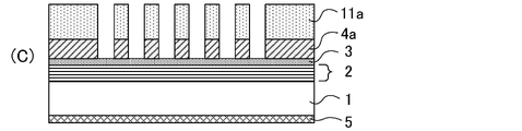
- 3A to 3D are process diagrams showing a process of manufacturing a reflective mask from a reflective mask blank in a schematic cross-sectional view of a main part. It is a figure which shows the value of the standardization evaluation function obtained by the simulation # 1a, in which the reflective mask has a vertical L / S (line and space) pattern of hp 16 nm, and is a RuNb film as a protective film (Cap film).
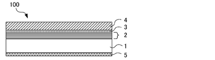
- FIG. 1 is a schematic cross-sectional view of a main part for explaining the configuration of the reflective mask blank 100 according to the embodiment of the present invention.
- the reflective mask blank 100 of the present embodiment includes a substrate 1, a multilayer reflective film 2 on the substrate 1, and an absorber film 4 on the multilayer reflective film 2.
- the surface of the substrate 1 on which the multilayer reflective film 2 is formed may be referred to as a first main surface (surface).
- the absorber film 4 of the reflective mask blank 100 of the present embodiment contains iridium (Ir) and a predetermined additive element.
- the reflective mask blank 100 of the present embodiment can have a protective film 3 between the multilayer reflective film 2 and the absorber film 4.
- a back surface conductive film 5 for an electrostatic chuck can be formed on the second main surface (back surface) side of the substrate 1.
- the reflective mask blank 100 of the present embodiment it is possible to form a transfer pattern having a fine pattern shape on the substrate to be transferred, and to obtain a transfer pattern capable of performing EUV exposure at a high throughput.
- a reflective mask 200 having a reflection type mask 200 can be manufactured. Further, specifically, it is possible to obtain a reflective mask blank 100 having an absorber film having a small refractive index (n), a high extinction coefficient (k), and good processing characteristics.
- the reflective mask blank 100 includes a configuration in which the back surface conductive film 5 is not formed. Further, the reflective mask blank 100 includes a mask blank with a resist film in which a resist film 11 is formed on an etching mask film.
- multilayer reflective film 2 on the substrate 1 means that the multilayer reflective film 2 is arranged in contact with the surface of the substrate 1, and also with the substrate 1. It also includes the case of having another film between the multilayer reflective film 2 and the multilayer reflective film 2. The same applies to other membranes.
- the film A is arranged in contact with the film B means that the film A and the film B are placed between the film A and the film B without interposing another film. It means that they are arranged so as to be in direct contact with each other.
- the substrate 1 preferably has a low coefficient of thermal expansion within the range of 0 ⁇ 5 ppb / ° C. in order to prevent distortion of the absorber pattern 4a due to heat during exposure to EUV light.
- a material having a low coefficient of thermal expansion in this range for example, SiO 2 -TIO 2 -based glass, multi-component glass ceramics, or the like can be used.
- the first main surface on the side where the transfer pattern of the substrate 1 (corresponding to the absorber pattern 4a in which the absorber film 4 described later is patterned) is formed is high from the viewpoint of obtaining at least the pattern transfer accuracy and the position accuracy.
- the surface is processed so that it has a flatness.
- the flatness is preferably 0.1 ⁇ m or less, more preferably 0.05 ⁇ m or less, and particularly preferably 0.05 ⁇ m or less in the region of 132 mm ⁇ 132 mm on the main surface on the side where the transfer pattern of the substrate 1 is formed. It is 0.03 ⁇ m or less.
- the second main surface on the side opposite to the side on which the absorber film 4 is formed is a surface that is electrostatically chucked when set in the exposure apparatus, and has a flatness of 0. It is preferably 1 ⁇ m or less, more preferably 0.05 ⁇ m or less, and particularly preferably 0.03 ⁇ m or less.
- the high surface smoothness of the substrate 1 is also an extremely important item.
- the surface roughness of the first main surface of the substrate 1 on which the transfer pattern (absorbent pattern 4a) is formed is preferably 0.1 nm or less in terms of root mean square roughness (RMS).
- RMS root mean square roughness
- the substrate 1 preferably has high rigidity in order to prevent deformation of the film (multilayer reflective film 2 or the like) formed on the substrate 1 due to film stress.
- those having a high Young's modulus of 65 GPa or more are preferable.
- the multilayer reflective film 2 imparts a function of reflecting EUV light in the reflective mask 200.
- the multilayer reflective film 2 is configured as a multilayer film in which each layer containing elements having different refractive indexes as main components is periodically laminated.
- a thin film of a light element or a compound thereof which is a high refractive index material and a thin film of a heavy element or a compound thereof (a low refractive index layer) which is a low refractive index material are alternately 40.
- a multilayer film laminated for about 60 cycles is used as the multilayer reflective film 2.
- the multilayer film may be laminated in a plurality of cycles with a laminated structure of a high refractive index layer / a low refractive index layer in which a high refractive index layer and a low refractive index layer are laminated in this order from the substrate 1 side as one cycle.
- the multilayer film may be laminated in a plurality of cycles with the laminated structure of the low refractive index layer / high refractive index layer in which the low refractive index layer and the high refractive index layer are laminated in this order from the substrate 1 side as one cycle.
- the outermost layer of the multilayer reflective film 2, that is, the surface layer of the multilayer reflective film 2 on the opposite side of the substrate 1 is preferably a high refractive index layer.
- the uppermost layer has low refraction. It becomes a rate layer.
- the low refractive index layer forms the outermost surface of the multilayer reflective film 2, it is easily oxidized, so that the reflectance of the reflective mask 200 decreases. Therefore, it is preferable to further form a high refractive index layer on the uppermost low refractive index layer to form the multilayer reflective film 2.
- the case where the laminated structure of the low refractive index layer / high refractive index layer in which the low refractive index layer and the high refractive index layer are laminated in this order from the substrate 1 side is one cycle is the most. Since the upper layer is a high refractive index layer, it can be left as it is.
- a layer containing silicon (Si) is adopted as the high refractive index layer.
- the material containing Si may be a Si compound containing boron (B), carbon (C), nitrogen (N), and oxygen (O) in addition to Si alone.
- a reflective mask 200 for EUV lithography having excellent reflectance of EUV light can be obtained.
- a glass substrate is preferably used as the substrate 1. Si is also excellent in adhesion to a glass substrate.
- a single metal selected from molybdenum (Mo), ruthenium (Ru), rhodium (Rh), and platinum (Pt), or an alloy thereof is used as the low refractive index layer.
- a Mo / Si periodic laminated film in which Mo film and Si film are alternately laminated for about 40 to 60 cycles is preferably used.
- a high-refractive index layer, which is the uppermost layer of the multilayer reflective film 2 is formed of silicon (Si), and a silicon oxide containing silicon and oxygen is formed between the uppermost layer (Si) and the Ru-based protective film 3. Layers may be formed. Thereby, the mask cleaning resistance can be improved.
- the reflectance of such a multilayer reflective film 2 alone is usually 65% or more, and the upper limit is usually 73%.
- the film thickness and period of each constituent layer of the multilayer reflective film 2 may be appropriately selected depending on the exposure wavelength, and are selected so as to satisfy Bragg's reflection law.
- the multilayer reflective film 2 there are a plurality of high refractive index layers and a plurality of low refractive index layers.
- the film thicknesses of the high refractive index layers and the low refractive index layers do not have to be the same.
- the film thickness of the Si layer on the outermost surface of the multilayer reflective film 2 can be adjusted within a range that does not reduce the reflectance.
- the film thickness of Si (high refractive index layer) on the outermost surface can be 3 nm to 10 nm.
- the method for forming the multilayer reflective film 2 is known in the art. For example, it can be formed by forming each layer of the multilayer reflective film 2 by an ion beam sputtering method.
- a Si film having a thickness of about 4 nm is first formed on the substrate 1 using a Si target. After that, a Mo film having a thickness of about 3 nm is formed using a Mo target.
- the Si film and the Mo film formed in this way are laminated for 40 to 60 cycles with one cycle as one cycle to form the multilayer reflective film 2 (the outermost layer is a Si layer).
- the multilayer reflective film 2 by supplying krypton (Kr) ion particles from an ion source and performing ion beam sputtering when the multilayer reflective film 2 is formed.
- the multilayer reflective film 2 is preferably about 40 cycles from the viewpoint of improving the reflectance by increasing the number of stacking cycles and reducing the throughput due to the increase in the number of steps.
- the number of layers of the multilayer reflective film 2 is not limited to 40, and may be, for example, 60. When 60 cycles are used, the number of steps is larger than that of 40 cycles, but the reflectance to EUV light can be increased.
- the reflective mask blank 100 of the present embodiment preferably has a protective film 3 between the multilayer reflective film 2 and the absorber film 4. Since the protective film 3 is formed on the multilayer reflective film 2, damage to the surface of the multilayer reflective film 2 when manufacturing the reflective mask 200 (EUV mask) using the reflective mask blank 100 is suppressed. can do. Therefore, by having the protective film 3, the reflectance characteristic for EUV light becomes good.
- the protective film 3 is formed on the multilayer reflective film 2 in order to protect the multilayer reflective film 2 from dry etching and cleaning in the manufacturing process of the reflective mask 200 described later. It also protects the multilayer reflective film 2 when the black defect of the absorber pattern 4a is corrected by using an electron beam (EB).
- the protective film 3 is made of a material that is resistant to etchants, cleaning liquids, and the like.
- FIG. 1 shows a case where the protective film 3 has one layer, a laminated structure having three or more layers is also possible. For example, it is possible to make the bottom layer and the top layer a layer made of the above-mentioned Ru-containing substance, and to form a protective film 3 in which a metal or alloy other than Ru is interposed between the bottom layer and the top layer.
- the protective film 3 may be made of a material containing ruthenium as a main component.
- the material of the protective film 3 can be a simple substance of Ru metal.
- the material of the protective film 3 is Ru, titanium (Ti), niobium (Nb), Rh (lodium), molybdenum (Mo), zirconium (Zr), yttrium (Y), boron (B), lanthanum (La). , Cobalt (Co), renium (Re) and the like, and can be a Ru alloy containing at least one metal. Further, the ru metal simple substance or the Ru alloy can further contain nitrogen.
- the absorber film 4 (or the buffer layer 42 described later) is used as an etching gas using a fluorine-based gas (F-based gas) or a chlorine-based gas containing no oxygen (Cl-based gas). It is effective when patterning by dry etching.
- the protective film 3 preferably has an etching selectivity of the absorber film 4 (etching rate of the absorber film 4 / etching rate of the protective film 3) with respect to the protective film 3 in dry etching using these etching gases. Is preferably formed of a material having 3 or more.
- Fluorine-based gases include CF 4 , CHF 3 , C 2 F 6 , C 3 F 6 , C 4 F 6 , C 4 F 8 , CH 2 F 2 , CH 3 F, C 3 F 8 , and SF 6 . / Or a gas such as F 2 can be used.
- gases such as Cl 2 , SiCl 4 , CHCl 3 , CCl 4 , and / or BCl 3 can be used.
- a mixed gas containing a fluorine-based gas and / or a chlorine-based gas and O 2 in a predetermined ratio can be used.
- These etching gases may further contain an inert gas such as He and / or Ar, if desired.
- the Ru content of the Ru alloy is 50 atomic% or more and less than 100 atomic%, preferably 80 atomic% or more and less than 100 atomic%, and more preferably 95 atomic% or more and less than 100 atomic%. be.
- the reflectance of EUV light is sufficient while suppressing the diffusion of the element (silicon) constituting the multilayer reflective film 2 to the protective film 3. Can be secured.
- this protective film 3 it is possible to have a mask cleaning resistance, an etching stopper function when the absorber film 4 is etched, and a function as a protective film 3 to prevent the multilayer reflective film 2 from changing with time. Become.
- the material of the protective film 3 can be a material containing silicon (Si).
- Materials containing silicon (Si) include, for example, silicon (Si), silicon oxide (Si xOy ( x and y are integers of 1 or more) such as SiO, SiO 2 , and Si 3 O 2 ), silicon nitride ( Si x N y ( x and y are integers of 1 or more) such as SiN and Si 3N4 , and silicon oxide (Si xOyN z such as SiON (x, y and z are integers of 1 or more)).
- Si silicon oxide
- Si xOyN z silicon oxide
- Such a protective film 3 is particularly effective when a buffer layer 42, which will be described later, is provided as a lower layer of the absorber film 4, and the buffer layer is patterned by dry etching of a chlorine-based gas (Cl-based gas) containing oxygen gas.
- the protective film 3 has an etching selectivity (etching rate of the absorber film 4 / etching rate of the protective film 3) of the absorber film 4 with respect to the protective film 3 in dry etching using a chlorine-based gas containing oxygen gas. As described above, it is preferably formed of a material having 3 or more.
- the protective film 3 is made of a material containing ruthenium (Ru) or silicon (Si).
- a material containing ruthenium (Ru) for example, Ru simple substance Ru alloy
- damage to the surface of the multilayer reflective film 2 can be effectively suppressed.
- the protective film 3 is formed of a material containing silicon (Si)
- the degree of freedom in selecting the material of the absorber film 4 can be increased.
- EUV lithography there are few substances that are transparent to the exposure light, so it is not technically easy to use EUV pellicle to prevent foreign matter from adhering to the mask pattern surface. For this reason, pellicle-less operation that does not use pellicle has become the mainstream. Further, in EUV lithography, exposure contamination occurs such that a carbon film is deposited on the mask and an oxide film is grown due to EUV exposure. Therefore, when the EUV reflective mask 200 is used in the manufacture of a semiconductor device, it is necessary to frequently perform cleaning to remove foreign matter and contamination on the mask. Therefore, the EUV reflective mask 200 is required to have an order of magnitude more mask cleaning resistance than the transmissive mask for optical lithography.
- the Ru-based protective film 3 containing Ti When the Ru-based protective film 3 containing Ti is used, cleaning resistance to a cleaning solution such as sulfuric acid, sulfuric acid hydrogen peroxide (SPM), ammonia, ammonia hydrogen peroxide (APM), OH radical cleaning water, or ozone water having a concentration of 10 ppm or less is used. Is particularly high, and it is possible to meet the requirement for mask cleaning resistance.
- a cleaning solution such as sulfuric acid, sulfuric acid hydrogen peroxide (SPM), ammonia, ammonia hydrogen peroxide (APM), OH radical cleaning water, or ozone water having a concentration of 10 ppm or less.
- the film thickness of the protective film 3 composed of such ruthenium (Ru) or an alloy thereof, silicon (Si) or the like is not particularly limited as long as it can function as the protective film 3. From the viewpoint of the reflectance of EUV light, the film thickness of the protective film 3 is preferably 1.0 nm to 8.0 nm, more preferably 1.5 nm to 6.0 nm.
- the same method as a known film forming method can be adopted without particular limitation.
- Specific examples include a sputtering method and an ion beam sputtering method.
- the absorber film 4 that absorbs EUV light is formed on the multilayer reflective film 2 or the protective film 3.
- the absorber film 4 has a function of absorbing EUV light.
- the absorber film 4 may be an absorber film 4 for the purpose of absorbing EUV light, or may be an absorber film 4 having a phase shift function in consideration of the phase difference of EUV light.
- the absorber film 4 used in the reflective mask blank 100 of the first embodiment will be described.
- the absorber film 4 of the reflective mask blank 100 of the present embodiment contains iridium (Ir) and an additive element.
- the reason why the absorber film 4 of the present embodiment contains iridium (Ir) will be described.
- An “evaluation function” is used as a guideline for selecting the material of the absorber film 4.
- the “evaluation function” is the product of the normalized image logarithmic gradient (NILS) and the threshold of light intensity for photosensitization of a predetermined resist.
- NILS normalized image logarithmic gradient
- a "normalized evaluation function” that standardizes the “evaluation function” can be used.
- the normalized image logarithmic gradient (NILS) is expressed as the following equation 1.
- W unit: nm
- I indicates the light intensity.
- I I threshold
- the normalized image logarithmic gradient may be simply referred to as "NILS”.
- the "normalized image logarithm gradient (NILS)" indicates the magnitude of the inclination when the horizontal axis is the position and the vertical axis is the logarithm of the light intensity of the exposure light. That is, the higher the NILS, the higher the contrast.
- EUV lithography a predetermined transfer pattern is transferred to a resist layer on a substrate to be transferred. The resist of the resist layer is exposed to light according to the dose amount of the exposure light (the light intensity is extended over time). Therefore, when the resist after exposure is developed, the higher the contrast (NILS), the larger the inclination of the shape of the pattern edge portion of the transfer pattern.
- the normalized image logarithmic gradient (NILS) is high in order to obtain a fine and highly accurate transfer pattern. Further, it can be said that the higher the normalized image logarithmic gradient (NILS) is, the finer the pattern-shaped transfer pattern can be formed on the substrate to be transferred.
- the transfer pattern formed on the substrate to be transferred may be referred to as a resist transfer pattern.
- the "threshold value" of the light intensity for photosensitization of a predetermined resist is a line-and-space pattern (may be simply referred to as “hp” in the present specification) of a predetermined half pitch (in the present specification, it may be simply referred to as “hp”). In the present specification, it may be simply referred to as “L / S”). It refers to the light intensity for exposing the resist at a predetermined hp during EUV exposure for forming the resist transfer pattern. ..
- the “threshold value” means the light intensity that the resist is exposed to at a predetermined hp.
- the threshold value is the light intensity at which the negative photosensitive material is completely insoluble when developed after exposure to a predetermined light intensity. means. The higher the threshold value, the smaller the dose amount of the exposure light during EUV exposure, and the higher the throughput of the EUV exposure process. Therefore, in order to increase the throughput of the EUV exposure process, it is preferable that the threshold value is high.
- the "evaluation function” is the product of the normalized image logarithmic gradient (NILS) and the threshold value of the light intensity for the exposure of a predetermined resist.
- NILS normalized image logarithmic gradient
- the "standardized evaluation function” is a film having a refractive index (n) of 0.95 and an extinction coefficient (k) of 0.03 with respect to EUV light having a wavelength of 13.5 nm (the present invention).
- the value of the evaluation function of the reflective mask 200 using the pattern (reference film pattern) of the “reference film”) as the absorber pattern 4a is set to 1, and the value of the evaluation function of the film to be compared is standardized. It means the ratio of the value of the evaluation function.
- the values of the "evaluation function” and the "normalized evaluation function” can be obtained by simulation. Therefore, when the refractive index (n) and the extinction coefficient (k) of the absorber film 4 (absorbent pattern 4a) of the reflective mask 200 are changed in the case of exposure with light having a wavelength of 13.5 nm by simulation. The value of the standardized evaluation function of was obtained.
- the reflective mask 200 used for the simulation is a multilayer reflective film 2 (4.2 nm Si film and 2.8 nm) composed of Mo and Si on a substrate 1 (SiO 2 -TiO 2 glass substrate). A pair of Mo films of No.
- the film thickness of the absorber pattern 4a was optimized so as to have the highest evaluation function value.
- FIG. 4 shows the above-mentioned simulation reflective mask 200 (protective film 3 is a RuNb film) obtained by simulation (simulation # 1a) in the case where the absorber pattern 4a is a vertical L / S (line and space) pattern of hp 16 nm.
- the value of the standardized evaluation function is shown.
- FIG. 4 shows a standardized evaluation function when a predetermined incident light is applied to an absorber pattern 4a having a different refractive index (n) and extinction coefficient (k) in the reflective mask 200 of simulation # 1a. It is a figure which shows the distribution of the value of. In the simulation shown in FIG.
- FIG. 4 shows the value of the standardized evaluation function in gray scale.
- FIG. 5 shows the distribution of the values of the normalized evaluation function obtained by combining all of the simulations # 1a to # 3a and # 1b to # 3b.
- FIG. 5 is a diagram showing a binarized distribution when the values of the normalized evaluation functions are all 1.015 or more (white) and in other cases (black) in all simulations.
- the regions where the values of the normalized evaluation functions are all 1.015 or more are , It can be understood that the region is shown as white in FIG.
- the elemental substances belonging to the region in which the values of the normalized evaluation functions are all 1.015 or more are Ag, Co, Pt, Au, Fe, Pd, Ir, W, Cr, Rh, Ru and the like. Therefore, if the absorber film 4 is formed using these materials, a finer pattern shape is formed on the transfer substrate as compared with the conventional absorber film 4 made of TaBN film, TaN film, or the like. It can be said that the transfer pattern of the above can be formed more reliably, and EUV exposure can be performed with a high throughput.
- the present inventor paid attention to the fact that iridium (Ir) is included in the region where the values of the normalized evaluation functions are all 1.015 or more.
- the etching rate of iridium (Ir) is slow and the workability is poor. Therefore, when the absorber film 4 composed of only Ir is used, there is a problem that it is not easy to form the absorber pattern 4a. Therefore, the present inventor has found that the problem of processability of Ir can be solved by using a material containing Ir and a predetermined additive element as the material of the absorber film 4 of the reflective mask blank 100.
- the reflective mask blank 100 having the predetermined absorber film 4 (absorbent film 4 containing Ir and predetermined additive elements) of the present embodiment a transfer pattern having a fine pattern shape is used on the substrate to be transferred. It is possible to manufacture a reflective mask 200 having a transfer pattern capable of forming an EUV exposure at a high throughput.
- the content of iridium (Ir) in the absorber film 4 is more than 50 atomic%, preferably 60 atomic% or more, and preferably 70 atomic% or more. More preferred.
- the refractive index of iridium (Ir) with respect to EUV light having a wavelength of 13.5 nm is 0.905, and the extinction coefficient is 0.044. That is, the extinction coefficient of iridium (Ir) is higher than that of tantalum (Ta) and the like, and the refractive index of iridium (Ir) is lower than that of tantalum (Ta) and the like.
- the iridium (Ir) content of the absorber film 4 is relatively high, it is possible to obtain a reflective mask 200 having a high contrast and a thin film thickness of the absorber pattern 4a. As a result, the shadowing effect during exposure can be reduced.
- the content (upper limit) of iridium (Ir) in the absorber film 4 is preferably 90 atomic% or less, and more preferably 80 atomic% or less.
- the absorber film 4 of this embodiment contains an additive element.
- Additive elements are boron (B), silicon (Si), phosphorus (P), titanium (Ti), germanium (Ge), arsenic (As), selenium (Se), niobium (Nb), molybdenum (Mo), ruthenium. At least one selected from (Ru) and tantalum (Ta).
- an appropriate etching gas for example, a fluorine-based etching gas
- Workability can be improved.
- the additive element contained in the absorber film 4 is preferably at least one selected from tantalum (Ta), molybdenum (Mo), niobium (Nb) and boron (B).
- Ta tantalum
- Mo molybdenum
- Nb niobium
- B boron
- the additive element contained in the absorber film 4 contains tantalum (Ta).
- iridium (Ir) is a material having compressive stress
- tantalum (Ta) having tensile stress as an additive element. Therefore, when the absorber film 4 contains tantalum (Ta), the absorber film 4 having a balanced stress can be obtained.
- tantalum (Ta) has been widely used as a material for the absorber film 4 of the reflective mask blank 100, and is highly reliable.
- the absorber film 4 containing iridium (Ir) and tantalum (Ta) can be easily etched by using a fluorine-based etching gas, and thus has good processability. Therefore, since the absorber film 4 contains tantalum (Ta), it is possible to obtain a reflective mask blank 100 having high reliability and good processability.
- the content of tantalum (Ta) in the absorber film 4 is preferably 2 atomic% or more, preferably 10 atomic%. The above is more preferable.
- the content of tantalum (Ta) is preferably 30 atomic% or less, more preferably 20 atomic% or less. Since the content of tantalum (Ta) in the absorber film 4 is 2 to 30 atomic%, it is possible to obtain the absorber film 4 having an excellent balance of optical characteristics, processing characteristics and stress.
- the B content in the absorber film 4 is preferably 2 atomic% or more, and more preferably 5 atomic% or more.
- the B content is preferably 25 atomic% or less, more preferably 20 atomic% or less.
- the Si content in the absorber film 4 is preferably 2 atomic% or more, and more preferably 5 atomic% or more.
- the Si content is preferably 25 atomic% or less, more preferably 20 atomic% or less.
- the P content in the absorber film 4 is preferably 2 atomic% or more, and more preferably 5 atomic% or more.
- the P content is preferably 20 atomic% or less, and more preferably 10 atomic% or less.
- the Ti content in the absorber film 4 is preferably 2 atomic% or more, and more preferably 10 atomic% or more.
- the Ti content is preferably 30 atomic% or less, more preferably 20 atomic% or less.
- the Ge content in the absorber film 4 is preferably 2 atomic% or more, and more preferably 5 atomic% or more.
- the Ge content is preferably 30 atomic% or less, more preferably 20 atomic% or less.
- the As content in the absorber film 4 is preferably 2 atomic% or more, and more preferably 5 atomic% or more.
- the As content is preferably 30 atomic% or less, more preferably 20 atomic% or less.
- the Se content in the absorber film 4 is preferably 2 atomic% or more, and more preferably 5 atomic% or more.
- the Se content is preferably 30 atomic% or less, more preferably 20 atomic% or less.
- the Nb content in the absorber film 4 is preferably 2 atomic% or more, more preferably 5 atomic% or more.
- the Nb content is preferably 30 atomic% or less, more preferably 25 atomic% or less.
- the Ru content in the absorber film 4 is preferably 2 atomic% or more, more preferably 5 atomic% or more.
- the Ru content is preferably 49 atomic% or less, more preferably 45 atomic% or less.
- the additive element contained in the absorber film 4 contains tantalum (Ta), and the Ir and Ta content ratio (Ir: Ta) is 4: 1 to 22: 1. It is preferably present, and more preferably 6: 1 to 15: 1.
- Ta tantalum
- the content ratio of Ir and Ta within a predetermined range, it is possible to ensure that the absorber film 4 having an excellent balance of optical characteristics, processing characteristics and stress can be obtained.
- the content ratio of Ir and B is preferably 3: 1 to 20: 1, preferably 4: 1 to 9: 1. Is more preferable.
- the Ir to Si content ratio (Ir: Si) is preferably 3: 1 to 20: 1, preferably 4: 1 to 9: 1. Is more preferable.
- the content ratio of Ir and P is preferably 4: 1 to 30: 1, and 9: 1 to 20: 1. Is more preferable.
- the Ir to Ti content ratio is preferably 2.2: 1 to 30: 1, preferably 4: 1 to 24. It is more preferable that it is 1.
- the content ratio (Ir: Ge) of Ir and Ge is preferably 2.2: 1 to 30: 1, preferably 4: 1 to 24. It is more preferable that it is 1.
- the content ratio (Ir: As) of Ir and As is preferably 2.2: 1 to 30: 1, preferably 4: 1 to 24. It is more preferable that it is 1.
- the content ratio (Ir: Se) of Ir and Se is preferably 2.2: 1 to 30: 1, preferably 4: 1 to 24. It is more preferable that it is 1.
- the content ratio (Ir: Nb) of Ir and Nb is preferably 2.2: 1 to 30: 1, preferably 4: 1 to 24. It is more preferable that it is 1.
- the content ratio of Ir and Mo is preferably 1.2: 1 to 9: 1, preferably 1.5: 1. It is more preferably ⁇ 4: 1.
- the content ratio of Ir and Ru is preferably 1.2: 1 to 9: 1, preferably 1.5: 1. It is more preferably ⁇ 4: 1.
- the absorber film 4 preferably further contains at least one selected from oxygen (O), nitrogen (N) and carbon (C). Further, the content of oxygen (O), nitrogen (N) and / or carbon (C) is preferably 5 atomic% or more, and more preferably 10 atomic% or more.
- oxygen (O), nitrogen (N) and / or carbon (C) is processed by etching of the absorber film 4 as compared with the absorber film 4 made of Ir alone. It is possible to improve the sex.
- the content of oxygen (O), nitrogen (N) and / or carbon (C) in the absorber film 4 is preferably 60 atomic% or less, more preferably 50 atomic% or less. It is more preferably 25 atomic% or less.
- the absorber film 4 of the reflective mask blank 100 of the present embodiment contains oxygen (O).
- the oxygen (O) content of the absorber film 4 is preferably 5 atomic% or more, and more preferably 10 atomic% or more.
- the upper limit of the oxygen (O) content in the absorber film 4 is preferably 60 atomic% or less, more preferably 50 atomic% or less, and further preferably 25 atomic% or less.
- the IrTaO film (absorbent film 4 ) containing oxygen (O) can be easily etched using a fluorine-based etching gas (for example, a mixed gas of CF4 gas and oxygen gas).
- a fluorine-based etching gas for example, a mixed gas of CF4 gas and oxygen gas.
- the refractive index of the material of the absorber film 4 is in the range of 0.86 to 0.95, and the extinction coefficient of the material of the absorber film 4 is in the range of 0.015 to 0.065. It is preferable to adjust the composition ratio of Ir and the added element so that the refractive index and the extinction coefficient of the absorber film 4 are within the above ranges.
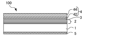
- the absorber film 4 of the reflective mask blank 100 of the present embodiment includes a buffer layer 42 containing chromium (Cr) and an absorption layer 44 provided on the buffer layer 42. Can be done.
- the material of the absorbent film 4 described above can be used as the material of the absorbent layer 44. That is, the absorption layer 44 can contain iridium (Ir) and an additive element.
- the buffer layer 42 can be arranged when the etching selectivity between the material of the absorption layer 44 (absorbent film 4) and the material of the multilayer reflective film 2 or the protective film 3 is not high. By arranging the buffer layer 42, the absorber pattern 4a can be easily formed, so that the absorber pattern 4a can be thinned. Further, the above-mentioned material of the absorber film 4 (material containing iridium (Ir) and additive elements) can be used as the material of the absorption layer 44. At this time, the material of the buffer layer 42 is preferably a material having an etching selectivity of 1.5 or more with respect to the material of the absorption layer 44. By providing the buffer layer 42, it is possible to broaden the selection of materials for the absorption layer 44 and the protective film 3 without reducing the effect of the present invention.
- a fluorine-based etching gas for example, a mixed gas of CF 4 gas and O 2 gas
- damage may occur to the protective film 3 (for example, Ru-based protective film).
- the absorber film 4 has a buffer layer 42 arranged between the absorption layer 44 and the protective film 3, and the buffer layer 42 contains chromium (Cr) to etch the absorption layer 44. Damage to the protective film 3 can be avoided.
- the material of the buffer layer 42 contains chromium (Cr) and one or more elements selected from oxygen (O), nitrogen (N), carbon (C), boron (B) and hydrogen (H). Can be a material to be used. Specific examples of the material of the buffer layer 42 include CrN, CrO, CrC, CrON, CrOC, CrCN, CrOCN and the like.
- the chromium-containing buffer layer 42 can be etched with a chlorine-based gas (for example, a mixed gas of Cl 2 gas and O 2 gas).
- the film thickness of the buffer layer 42 is preferably 1/3 or less of the film thickness of the entire absorber film 4 (absorbent layer 44 and buffer layer 42).
- the film thickness of the buffer layer 42 is preferably 10 nm or less, and more preferably 5 nm or less.
- the lower limit of the film thickness of the buffer layer 42 can be 2 nm or more, preferably 3 nm or more.
- the film thickness of the buffer layer 42 reduces the influence on the optical characteristics of the absorption layer 44 and has an effect as the buffer layer 42. It is preferable to make the film thickness close to the minimum for playing.
- the reflective mask blank 100 of the second embodiment includes a substrate 1, a multilayer reflective film 2 on the substrate 1, and an absorber film 4 on the multilayer reflective film 2.
- the absorber film 4 includes an uppermost layer and other lower layers.
- the film thickness of the uppermost layer is 0.5 nm or more and less than 5 nm.
- the uppermost layer may contain iridium (Ir) alone or iridium (Ir) and the additive element.
- the additive elements include boron (B), silicon (Si), phosphorus (P), titanium (Ti), germanium (Ge), arsenic (As), selenium (Se), niobium (Nb), molybdenum (Mo), and the like. At least one selected from ruthenium (Ru) and tantalum (Ta).
- the material of the absorber film 4 of the first embodiment material containing iridium (Ir) and additive elements
- the lower layer of the absorber film 4 of the second embodiment is not particularly limited as long as it is a material having a function of absorbing EUV light and having etching selectivity with respect to the protective film 3.
- Such materials include palladium (Pd), silver (Ag), platinum (Pt), gold (Au), tungsten (W), chromium (Cr), cobalt (Co), manganese (Mn), tin (Sn).
- the lower layer of the absorber film 4 of the second embodiment has Ag, Co, Pt, Au, Fe, Pd, W, Cr, which belong to the region where the value of the above-mentioned standardized evaluation function is 1.015 or more.
- An alloy containing at least one metal selected from Rh and Ru and two or more metals or a compound thereof can be preferably used.
- the lower layer of the absorber film 4 preferably contains the above metal or alloy in an amount of more than 50 atomic%, more preferably 60 atomic% or more.
- the compound may contain oxygen (O), nitrogen (N), carbon (C) and / or boron (B) in the metal or alloy.
- the reflectance of EUV light to the absorber film 4 is 2% or less, preferably 1% or less.
- the film thickness is set.
- the film thickness of the absorber film 4 of the reflective mask blank 100 of the first and second embodiments is preferably 50 nm or less, more preferably 45 nm or less.
- the film thickness of the absorber film 4 of the reflective mask blank 100 is 50 nm or less, the shadowing effect at the time of EUV exposure can be reduced.
- the lower limit of the film thickness of the absorber film 4 can be 35 nm or more, preferably 40 nm or more.
- the absorber film 4 of the first and second embodiments can be formed by a sputtering method (co-sputtering method) using an Ir target and a target of an additive element alone.
- the absorber film 4 can be formed by a sputtering method using an alloy target composed of Ir and an additive element.
- the reflective mask blank 100 of the present embodiment can include an etching mask film.
- the film thickness of the etching mask film is 0.5 nm or more and 14 nm or less.
- the etching mask film is formed on the absorber film 4.
- a material having a high etching selectivity of the absorber film 4 with respect to the etching mask film is used.
- the "etching selection ratio of B to A” refers to the ratio of the etching rate between A, which is a layer (mask layer) that is not desired to be etched, and B, which is a layer that is desired to be etched.
- etching selectivity of B with respect to A etching rate of B / etching rate of A”.
- high selection ratio means that the value of the selection ratio in the above definition is large with respect to the comparison target.
- the etching selectivity of the absorption layer 44 with respect to the etching mask film is preferably 1.5 or more, and more preferably 3 or more.
- the material of the etching mask film is selected from chromium (Cr), oxygen (O), nitrogen (N), carbon (C), boron (B) and hydrogen (H). It is preferable that the material contains one or more elements.
- Specific examples of the etching mask film include CrN, CrO, CrC, CrON, CrOC, CrCN and CrOCN.
- the film thickness of the etching mask film is 0.5 nm or more, preferably 1 nm or more, and preferably 2 nm or more, from the viewpoint of obtaining a function as an etching mask that accurately forms a transfer pattern on the absorber film 4. Is more preferable, and 3 nm or more is further preferable. Further, from the viewpoint of reducing the film thickness of the resist film 11, the film thickness of the etching mask film is preferably 14 nm or less, preferably 12 nm or less, and more preferably 10 nm or less.
- the etching mask film and the buffer layer 42 may be made of the same material. Further, the etching mask film and the buffer layer 42 may be made of materials containing the same metal but having different composition ratios.
- the etching mask film and the buffer layer 42 may contain chromium, the chromium content of the etching mask film is higher than the chromium content of the buffer layer 42, and the film thickness of the etching mask film is made thicker than the film thickness of the buffer layer 42. May be good.
- the etching mask film and the buffer layer 42 contain hydrogen, the hydrogen content of the etching mask film may be higher than the hydrogen content of the buffer layer 42.
- the reflective mask blank 100 of the present embodiment can have the resist film 11 on the etching mask film.
- the reflective mask blank 100 of the present embodiment also includes a form having a resist film 11.
- the resist film 11 can be thinned by selecting an absorbent film 4 and an etching gas having an appropriate material and / or an appropriate film thickness.
- the material of the resist film 11 for example, a chemically amplified resist (CAR) can be used.
- CAR chemically amplified resist
- a back surface conductive film 5 for an electrostatic chuck is formed on the second main surface (back surface) side of the substrate 1 (the surface opposite to the surface on which the multilayer reflective film 2 is formed).
- the electrical characteristics (sheet resistance) required for the back surface conductive film 5 for an electrostatic chuck are usually 100 ⁇ / ⁇ ( ⁇ / Square) or less.
- a magnetron sputtering method and an ion beam sputtering method can be used as a method for forming the back surface conductive film 5, for example.
- the target for sputtering can be selected from metal targets such as chromium (Cr) and tantalum (Ta), targets of alloys thereof, and the like.
- the material containing chromium (Cr) in the back surface conductive film 5 is preferably a Cr compound containing at least one selected from boron, nitrogen, oxygen, and carbon in Cr.
- the Cr compound include CrN, CrON, CrCN, CrCON, CrBN, CrBON, CrBCN and CrBOCN.
- Ta tantalum
- an alloy containing Ta or a Ta compound containing at least one of boron, nitrogen, oxygen, and carbon in any of these is used.
- the Ta compound include TaB, TaN, TaO, TaON, TaCON, TaBN, TaBO, TaBON, TaBCON, TaHf, TaHfO, TaHfN, TaHfON, TaHfCON, TaSi, TaSiO, TaSiN, TaSiN, and TaSiN. can.
- the amount of nitrogen (N) present in the surface layer is small.
- the nitrogen content of the surface layer of the back surface conductive film 5 of the material containing tantalum (Ta) or chromium (Cr) is preferably less than 5 atomic%, and the surface layer does not substantially contain nitrogen. Is more preferable. This is because, in the back surface conductive film 5 of a material containing tantalum (Ta) or chromium (Cr), the smaller the nitrogen content in the surface layer, the higher the wear resistance.
- the back surface conductive film 5 is preferably made of a material containing tantalum and boron. Since the back surface conductive film 5 is made of a material containing tantalum and boron, a back surface conductive film 5 having wear resistance and chemical resistance can be obtained.
- the back surface conductive film 5 contains tantalum (Ta) and boron (B), the B content is preferably 5 to 30 atomic%.
- the ratio of Ta and B (Ta: B) in the sputtering target used for forming the back surface conductive film 5 is preferably 95: 5 to 70:30.
- the film thickness of the back surface conductive film 5 is not particularly limited as long as it satisfies the function for the electrostatic chuck.
- the film thickness of the back surface conductive film 5 is usually 10 nm to 200 nm.
- the back surface conductive film 5 also has stress adjustment on the second main surface side of the mask blank 100. That is, the back surface conductive film 5 is adjusted so as to obtain a flat reflective mask blank 100 by balancing the stress from various films formed on the first main surface side.
- the present embodiment is a reflective mask 200 having an absorber pattern 4a in which the absorber film 4 of the above-mentioned reflective mask blank 100 is patterned.
- the reflective mask 200 of the present embodiment it is possible to form a transfer pattern having a fine pattern shape on the substrate to be transferred, and EUV exposure can be performed with a high throughput.
- the absorber pattern 4a of the reflective mask 200 absorbs EUV light, and the opening of the absorber pattern 4a can reflect EUV light. Therefore, by irradiating the reflective mask 200 with EUV light using a predetermined optical system, a predetermined fine transfer pattern can be transferred to the object to be transferred.
- the reflective mask 200 can be manufactured by patterning the absorber film 4 of the reflective mask blank 100 of the present embodiment.
- the method for manufacturing the reflective mask 200 will be described, and later, in the examples, the details will be described with reference to the drawings.
- a resist film 11 is formed on the absorber film 4 on the first main surface of the reflective mask blank 100 (unnecessary when the resist film 11 is provided as the reflective mask blank 100).
- a desired pattern is drawn (exposed) on the resist film 11 and further developed and rinsed to form a predetermined resist pattern 11a.
- the absorber pattern 4a is formed by etching the absorber film 4 with the resist pattern 11a as a mask.
- the resist pattern 11a is peeled off by a wet treatment such as oxygen ashing or hot sulfuric acid. Finally, wet cleaning is performed using an acidic or alkaline aqueous solution.
- the reflective mask 200 of the present embodiment can be manufactured.
- the reflective mask 200 of the present embodiment is set in an exposure device having an exposure light source that emits EUV light, and a transfer pattern is applied to a resist layer formed on a substrate to be transferred. It has a transfer step. According to the method for manufacturing a semiconductor device of the present embodiment, it is possible to form a transfer pattern having a fine pattern shape on a substrate to be transferred, and EUV exposure can be performed with a high throughput.
- the reflective mask 200 of the present embodiment it is possible to form a transfer pattern having a fine pattern shape on the substrate to be transferred. Further, by using the reflective mask 200 of the present embodiment, EUV exposure can be performed with a high throughput.
- a desired pattern can be formed on a semiconductor substrate with high dimensional accuracy and high throughput.
- a desired electronic circuit is formed by undergoing various processes such as etching of a film to be processed, formation of an insulating film and a conductive film, introduction of a dopant, and annealing. can.
- the EUV exposure apparatus is composed of a laser plasma light source that generates EUV light, an illumination optical system, a mask stage system, a reduced projection optical system, a wafer stage system, vacuum equipment, and the like.
- the light source is equipped with a debris trap function, a cut filter that cuts long wavelength light other than exposure light, and equipment for vacuum differential exhaust.
- the illumination optical system and the reduced projection optical system are composed of reflective mirrors.
- the EUV exposure reflective mask 200 is electrostatically adsorbed by the back surface conductive film 5 formed on its second main surface (back surface) and placed on the mask stage.
- the light from the EUV light source is applied to the reflective mask 200 at an angle of 6 ° to 8 ° with respect to the vertical surface of the reflective mask 200 via the illumination optical system.
- the reflected light from the reflective mask 200 with respect to the incident light is reflected (specularly reflected) in the direction opposite to the incident and at the same angle as the incident angle.
- the reflected light is usually guided to a reflective projection optical system having a reduction ratio of 1/4, and the resist layer on the wafer (semiconductor substrate) placed on the wafer stage is exposed. During this time, at least the place where EUV light passes is evacuated.
- the scan exposure in which the mask stage and the wafer stage are scanned in synchronization at a speed corresponding to the reduction ratio of the reduction projection optical system and the exposure is performed through the slit is the mainstream.
- a resist transfer pattern can be formed on the semiconductor substrate.
- a predetermined wiring pattern can be formed, for example, on a semiconductor substrate.
- a semiconductor device is manufactured through such necessary steps such as an exposure step, a film processing step to be processed, a forming step of an insulating film or a conductive film, a dopant introducing step, an annealing step, and the like.
- Experiments 1--7 a thin film corresponding to the absorber film 4 (referred to as “experimental absorber film”) was produced.
- the composition By evaluating the composition, film thickness, optical characteristics (refractive index (n) and extinction coefficient (k)), film stress and etching characteristics of the experimental absorber membranes of Experiments 1 to 7, the experimental absorber membrane was evaluated. The quality of use as a product was evaluated.
- the experimental absorber films of Experiments 5 and 6 are the absorber films 4 used in the reflective mask blanks 100 of Examples 1 and 2.
- Table 1 shows the materials and compositions of the experimental absorber membranes of Experiments 1 to 7.
- the experimental absorber membrane of Experiment 7 is a thin film composed of only Ir, and is an experimental absorber membrane for comparison with Experiments 1 to 6.
- a substrate with a multilayer reflective film having a substrate 1, a multilayer reflective film 2, and a protective film 3 was manufactured.
- the back surface conductive film 5 was formed on the back surface of the substrate 1.
- An experimental absorber film was formed so as to be placed in contact with the protective film 3 of the substrate with the multilayer reflective film. Therefore, the structure of the experimental absorber film after formation is the same as that of the reflective mask blank 100 shown in FIG.
- SiO 2 -TiO 2 glass substrate which is a 6025 size (about 152 mm ⁇ 152 mm ⁇ 6.35 mm) low thermal expansion glass substrate with both the first main surface and the second main surface polished, and use it as the substrate 1. did. Polishing was performed by a rough polishing process, a precision polishing process, a local processing process, and a touch polishing process so that the main surface was flat and smooth.
- a back surface conductive film 5 made of a CrN film was formed on the second main surface (back surface) of the SiO 2 -TiO 2 system glass substrate 1 by a magnetron sputtering (reactive sputtering) method under the following conditions.
- Conditions for forming the back surface conductive film 5 Cr target, mixed gas atmosphere of Ar and N 2 (Ar: 90%, N: 10%), film thickness 20 nm.
- the multilayer reflective film 2 was formed on the main surface (first main surface) of the substrate 1 on the side opposite to the side on which the back surface conductive film 5 was formed.
- the multilayer reflective film 2 formed on the substrate 1 is a periodic multilayer reflective film 2 composed of Mo and Si in order to make the multilayer reflective film 2 suitable for EUV light having a wavelength of 13.5 nm.
- the multilayer reflective film 2 was formed by alternately laminating Mo layers and Si layers on a substrate 1 by an ion beam sputtering method in an Ar gas atmosphere using a Mo target and a Si target. First, a Si film was formed with a film thickness of 4.2 nm, and then a Mo film was formed with a film thickness of 2.8 nm. This was set as one cycle, and the layers were laminated for 40 cycles in the same manner, and finally a Si film was formed with a film thickness of 4.0 nm to form a multilayer reflective film 2.
- a protective film 3 made of a RuNb film was formed with a film thickness of 3.5 nm by an ion beam sputtering method using a RuNb target.
- the substrates with the multilayer reflective film used in Experiments 1 to 7 were manufactured.
- a buffer layer 42 made of CrON was formed on the protective film 3. Specifically, first, a buffer layer 42 made of a CrON film was formed by a DC magnetron sputtering method. The CrON film was formed with a film thickness of 6 nm by reactive sputtering in a mixed gas atmosphere of Ar gas, O 2 gas and N 2 gas using a Cr target.
- an experimental absorber film of the materials shown in Table 1 was formed. Specifically, an experimental absorber film was formed by the DC magnetron sputtering method using the target and the sputtering gas shown in Table 2. In the case of Experiments 5 and 6 containing oxygen (O), an experimental absorber film was formed by reactive sputtering using a sputtering gas containing O 2 gas.
- the elemental composition (atomic%) of the experimental absorber membranes of Experiments 1 to 7 was measured by X-ray photoelectron spectroscopy (XPS method).
- the elemental composition (atomic%) of the thin film may be referred to as “composition” or “composition ratio”.
- the film thickness of the experimental absorber film of Experiments 1 to 7 was measured by XRR (X-ray reflectivity method).
- the refractive index (n) and extinction coefficient (k) of the experimental absorber films of Experiments 1 to 7 at a wavelength of 13.5 nm were measured by an EUV reflectance meter.
- the film stress in Experiments 1 to 7 was evaluated by measuring the flatness of the experimental absorber film before and after film formation with a flatness measuring device (UltraFlat200 manufactured by Tropel Co., Ltd.) and comparing the two. Specifically, the film stress was evaluated by taking the difference between the flatness of the experimental absorber film before film formation and the flatness after film formation. Table 1 shows the measurement results of the difference in flatness.
- the experimental absorber membrane of Experiment 7 is a thin film composed of only Ir, and is an experimental absorber membrane for comparison with Experiments 1 to 6.
- the extinction coefficient (k) of the experimental absorber films of Experiments 1 to 6 at a wavelength of 13.5 nm was more than 0.03.
- the extinction coefficient (k) of the TaBN film used as the absorber film 4 of Comparative Example 1 described later at a wavelength of 13.5 nm is 0.03.
- the TaBN film is one of the materials currently generally used as the absorber film 4 of the reflective mask blank 100. Therefore, it can be said that the absorber membrane 4 having a high extinction coefficient (k) can be obtained by using the experimental absorber membrane having the compositions of Experiments 1 to 6 as the absorber membrane 4.
- the experimental absorber membrane of Experiment 7 also has a high extinction coefficient (k) as in Experiments 1 to 6.
- the refractive index (n) of the experimental absorber films of Experiments 1 to 6 at a wavelength of 13.5 nm was less than 0.95.
- the refractive index (n) of the TaBN film used as the absorber film 4 of Comparative Example 1 described later at a wavelength of 13.5 nm is 0.95. Therefore, it can be said that the absorber film 4 having a low refractive index (n) can be obtained by using the experimental absorber film having the compositions of Experiments 1 to 6 as the absorber film 4.
- the experimental absorber film of Experiment 7 also has a low refractive index (n) as in Experiments 1 to 6.
- the difference in flatness of the experimental absorber films of Experiments 1 to 6 was 300 nm or less.
- the difference in flatness of the experimental absorber film of Experiment 7 material: Ir was 811 nm. Therefore, by using the experimental absorber films of Experiments 1 to 6 as the absorber film 4, it is possible to obtain the absorber film 4 capable of adjusting the film stress and suppressing the deformation of the reflective mask blank 100. It can be said that it can be done.
- the relative etching rate of the experimental absorber film of Experiments 1 to 6 is 1.3 when the etching rate of the experimental absorber film of Experiment 7 (material: Ir) is 1. It was ⁇ 1.8. Therefore, it can be said that by using the experimental absorber films of Experiments 1 to 6 as the absorber film 4, it is possible to obtain the absorber film 4 having a high etching rate and good processability.
- Example 1 As Example 1, a thin film having the same composition and thickness as the experimental absorber film of Experiment 5 was formed as the absorber film 4 to produce a reflective mask 200.
- the reflective mask blank 100 of the first embodiment has a back surface conductive film 5, a substrate 1, a multilayer reflective film 2, a protective film 3, and an absorber film 4 (buffer layer 42 and an absorbent layer). 44) and.
- the structure in which the resist film 11 is formed on the absorber film 4 is also the reflective mask blank 100 of the present embodiment.
- 3A to 3D are schematic cross-sectional views of a main part showing a step of manufacturing a reflective mask 200 from a reflective mask blank 100.
- a SiO 2 -TIO 2 system glass substrate was prepared and used as the substrate 1. Similar to Experiments 1 to 7, polishing including a rough polishing process, a precision polishing process, a local processing process, and a touch polishing process was performed.
- the back surface conductive film 5 made of a CrN film is attached to the second main surface (back surface) of the SiO 2 -TiO 2 system glass substrate 1 by the magnetron sputtering (reactive sputtering) method as described below. It was formed under the conditions. Conditions for forming the back surface conductive film 5: Cr target, mixed gas atmosphere of Ar and N 2 (Ar: 90%, N: 10%), film thickness 20 nm.
- the Si layer (4.2 nm) and the Mo layer (2) are placed on the main surface (first main surface) of the substrate 1 on the side opposite to the side on which the back surface conductive film 5 is formed. (0.8 nm) was alternately laminated for 40 cycles, and finally a Si film was formed with a film thickness of 4.0 nm to form a multilayer reflective film 2.
- a protective film 3 made of a RuNb film was formed with a film thickness of 3.5 nm.
- a buffer layer 42 made of CrON was formed on the protective film 3.
- the CrON film was formed into a film having a film thickness of 6 nm by reactive sputtering in a mixed gas atmosphere of Ar gas, O 2 gas and N 2 gas using a Cr target.
- the reflective mask blank 100 of Example 1 was manufactured.
- the absorption layer 44 of the reflective mask blank 100 of Example 1 is the same thin film as the experimental absorber film of Experiment 5. Therefore, by using the reflective mask blank 100 of Example 1, it is possible to form a transfer pattern having a fine pattern shape on the substrate to be transferred, and EUV exposure can be performed at a high throughput for transfer. It can be said that the reflective mask 200 having a pattern can be manufactured.
- the reflective mask 200 of Example 1 was manufactured using the reflective mask blank 100 of Example 1.
- a resist film 11 having a thickness of 80 nm was formed on the absorber film 4 of the reflective mask blank 100 (FIG. 3A).
- a chemically amplified resist (CAR) was used to form the resist film 11.
- a desired pattern was drawn (exposed) on the resist film 11 and further developed and rinsed to form a predetermined resist pattern 11a (FIG. 3B).
- dry etching of the absorption layer 44 IrTaO film
- CF 4 + O 2 gas CF 4 + O 2 gas
- dry etching of the CrON film buffer layer 42
- mask defects can be inspected after wet cleaning and mask defects can be corrected as appropriate.
- the reflective mask 200 of Example 1 was set in an EUV scanner, and EUV exposure was performed on a wafer having a film to be processed and a resist layer formed on a semiconductor substrate. Then, by developing the exposed resist of the resist layer, a resist transfer pattern was formed on the semiconductor substrate on which the film to be processed was formed.
- This resist transfer pattern is transferred to a film to be processed by etching, and a semiconductor device having desired characteristics is manufactured by undergoing various steps such as formation of an insulating film and a conductive film, introduction of a dopant, and annealing. Was made.
- Example 2 is the same as that of Example 1, but a thin film having the same composition and thickness as the experimental absorber film of Experiment 6 is formed as the absorption layer 44, and the reflective mask blank 100 and the reflective mask 200 are formed.
- the absorption layer 44 IrTaO film, film thickness 40 nm
- the reflective mask blank 100 of Example 2 includes an absorber film 4 composed of a buffer layer 42 of a CrON film and an absorption layer 44 of an IrTaO film.
- the absorption layer 44 of the reflective mask blank 100 of Example 2 is the same thin film as the experimental absorber film of Experiment 6. Therefore, by using the reflective mask blank 100 of Example 2, it is possible to form a transfer pattern having a fine pattern shape on the substrate to be transferred, and EUV exposure can be performed at a high throughput for transfer. It can be said that the reflective mask 200 having a pattern can be manufactured.
- a resist transfer pattern on the substrate to be transferred using the reflective mask 200 of Example 2 it is possible to form a transfer pattern having a fine pattern shape, and EUV exposure can be performed at a high throughput. I was able to confirm that I could do it.
- the absorber film 4 of the reflective mask blank 100 of Comparative Example 1 is a TaBN film.
- the extinction coefficient (k) of this TaBN film at a wavelength of 13.5 nm was 0.03, and the refractive index (n) was 0.95. Therefore, the extinction coefficient (k) of the absorber film 4 of Comparative Example 1 is lower than the extinction coefficient (k) of the absorber membrane 4 of Examples 1 and 2. Further, the refractive index (n) of the absorber film 4 of Comparative Example 1 is higher than the refractive index (n) of the absorber films 4 of Examples 1 and 2. Further, as shown in FIG.
- the value of the standardized evaluation function when the thin film containing Ta is used as the absorber film 4 is the value of the standardized evaluation function when the thin film containing Ir is used as the absorber film 4. It is clear that it is higher than that. Therefore, when the reflective mask blank 100 of Comparative Example 1 is used, it is not easy to form a transfer pattern having a fine pattern shape on the substrate to be transferred as compared with the cases of Examples 1 and 2. , It cannot be said that EUV exposure can be performed with a high throughput.
Landscapes
- Physics & Mathematics (AREA)
- General Physics & Mathematics (AREA)
- Engineering & Computer Science (AREA)
- Condensed Matter Physics & Semiconductors (AREA)
- Manufacturing & Machinery (AREA)
- Computer Hardware Design (AREA)
- Microelectronics & Electronic Packaging (AREA)
- Power Engineering (AREA)
- Preparing Plates And Mask In Photomechanical Process (AREA)
- Exposure Of Semiconductors, Excluding Electron Or Ion Beam Exposure (AREA)
- Exposure And Positioning Against Photoresist Photosensitive Materials (AREA)
Abstract
Description
本実施形態の構成1は、基板と、該基板上の多層反射膜と、該多層反射膜上の吸収体膜とを備える反射型マスクブランクであって、
前記吸収体膜は、イリジウム(Ir)と、添加元素とを含み、
前記添加元素は、ホウ素(B)、ケイ素(Si)、リン(P)、チタン(Ti)、ゲルマニウム(Ge)、ヒ素(As)、セレン(Se)、ニオブ(Nb)、モリブデン(Mo)、ルテニウム(Ru)及びタンタル(Ta)から選択される少なくとも1つであり、
前記吸収体膜中の前記イリジウム(Ir)の含有量は50原子%超であることを特徴とする反射型マスクブランクである。
本実施形態の構成2は、前記添加元素は、タンタル(Ta)を含むことを特徴とする構成1の反射型マスクブランクである。
本実施形態の構成3は、前記添加元素はタンタル(Ta)を含み、前記吸収体膜中の前記タンタル(Ta)の含有量は2~30原子%であることを特徴とする構成1又は2の反射型マスクブランクである。
本実施形態の構成4は、前記吸収体膜は、さらに酸素(O)を含み、前記酸素(O)の含有量は5原子%以上であることを特徴とする構成1乃至3の何れか記載の反射型マスクブランクである。
本実施形態の構成5は、前記吸収体膜は、バッファ層と、バッファ層の上に設けられた吸収層とを含み、
前記バッファ層は、クロム(Cr)を含み、
前記吸収層は、前記イリジウム(Ir)と、前記添加元素とを含むことを特徴とする構成1乃至4の何れかの反射型マスクブランクである。
本実施形態の構成6は、前記吸収体膜の膜厚は、50nm以下であり、前記バッファ層の膜厚は、10nm以下であることを特徴とする構成5の反射型マスクブランクである。
本実施形態の構成7は、構成1乃至6の何れかの反射型マスクブランクにおける前記吸収体膜がパターニングされた吸収体パターンを有することを特徴とする反射型マスクである。
本実施形態の構成8は、構成1乃至6の何れかの反射型マスクブランクの前記吸収体膜をパターニングして吸収体パターンを形成することを特徴とする反射型マスクの製造方法である。
本実施形態の構成9は、EUV光を発する露光光源を有する露光装置に、構成7の反射型マスクをセットし、被転写基板上に形成されているレジスト膜に転写パターンを転写する工程を有することを特徴とする半導体装置の製造方法である。
図1は、本発明の実施形態の反射型マスクブランク100の構成を説明するための要部断面模式図である。図1に示すように、本実施形態の反射型マスクブランク100は、基板1と、基板1の上の多層反射膜2と、多層反射膜2の上の吸収体膜4とを備える。本明細書では、多層反射膜2が形成される基板1の表面のことを、第1主面(表面)という場合がある。本実施形態の反射型マスクブランク100の吸収体膜4は、イリジウム(Ir)と、所定の添加元素とを含む。本実施形態の反射型マスクブランク100は、多層反射膜2と吸収体膜4との間に、保護膜3を有することができる。また、基板1の第2主面(裏面)側には、静電チャック用の裏面導電膜5を形成することができる。
基板1は、EUV光による露光時の熱による吸収体パターン4aの歪みを防止するため、0±5ppb/℃の範囲内の低熱膨張係数を有するものが好ましく用いられる。この範囲の低熱膨張係数を有する素材としては、例えば、SiO2-TiO2系ガラス、多成分系ガラスセラミックス等を用いることができる。
多層反射膜2は、反射型マスク200において、EUV光を反射する機能を付与する。多層反射膜2は、屈折率の異なる元素を主成分とする各層が周期的に積層された多層膜の構成である。
本実施形態の反射型マスクブランク100は、多層反射膜2と吸収体膜4との間に、保護膜3を有することが好ましい。多層反射膜2の上に保護膜3が形成されていることにより、反射型マスクブランク100を用いて反射型マスク200(EUVマスク)を製造する際の多層反射膜2の表面へのダメージを抑制することができる。そのため、保護膜3を有することにより、EUV光に対する反射率特性が良好となる。
本実施形態の反射型マスクブランク100では、多層反射膜2又は保護膜3の上に、EUV光を吸収する吸収体膜4が形成される。吸収体膜4は、EUV光を吸収する機能を有する。吸収体膜4は、EUV光の吸収を目的とした吸収体膜4であってもよいし、EUV光の位相差も考慮した位相シフト機能を有する吸収体膜4であっても良い。

本実施形態の反射型マスクブランク100は、エッチングマスク膜を含むことができる。エッチングマスク膜の膜厚は0.5nm以上14nm以下である。
本実施形態の反射型マスクブランク100は、エッチングマスク膜の上にレジスト膜11を有することができる。本実施形態の反射型マスクブランク100には、レジスト膜11を有する形態も含まれる。本実施形態の反射型マスクブランク100では、適切な材料及び/又は適切な膜厚の吸収体膜4及びエッチングガスを選択することにより、レジスト膜11の薄膜化が可能である。
基板1の第2主面(裏面)側(多層反射膜2を形成する表面の反対側の表面)には、一般的に、静電チャック用の裏面導電膜5が形成される。静電チャック用の裏面導電膜5に求められる電気的特性(シート抵抗)は通常100Ω/□(Ω/Square)以下である。裏面導電膜5の形成方法としては、例えばマグネトロンスパッタリング法及びイオンビームスパッタリング法を用いることができる。スパッタリングの際のターゲットは、クロム(Cr)及びタンタル(Ta)等の金属ターゲット、並びにそれらの合金のターゲットなどから選択することができる。
本実施形態は、上述の反射型マスクブランク100の吸収体膜4がパターニングされた吸収体パターン4aを有する反射型マスク200である。本実施形態の反射型マスク200を用いることにより、被転写基板上に微細なパターン形状の転写パターンを形成することが可能であり、かつEUV露光を高いスループットで行うことができる。
本実施形態の半導体装置の製造方法は、EUV光を発する露光光源を有する露光装置に、本実施形態の反射型マスク200をセットし、被転写基板上に形成されているレジスト層に転写パターンを転写する工程を有する。本実施形態の半導体装置の製造方法より、被転写基板上に微細なパターン形状の転写パターンを形成することが可能であり、かつEUV露光を高いスループットで行うことができる。
実験1~7では、吸収体膜4に相当する薄膜(「実験用吸収体膜」という。)を製造した。実験1~7の実験用吸収体膜の組成、膜厚、光学特性(屈折率(n)及び消衰係数(k))、膜応力及びエッチング特性、を評価することにより、実験用吸収体膜としての使用の良否を評価した。なお、実験5及び6の実験用吸収体膜は、実施例1及び2の反射型マスクブランク100に用いられる吸収体膜4である。
裏面導電膜5の形成条件:Crターゲット、ArとN2の混合ガス雰囲気(Ar:90%、N:10%)、膜厚20nm。
実施例1として、実験5の実験用吸収体膜と同じ組成及び膜厚の薄膜を、吸収体膜4として形成して、反射型マスク200を製造した。
裏面導電膜5の形成条件:Crターゲット、ArとN2の混合ガス雰囲気(Ar:90%、N:10%)、膜厚20nm。
実施例2として、実施例1と同様であるが、実験6の実験用吸収体膜と同じ組成及び膜厚の薄膜を、吸収層44として形成して、反射型マスクブランク100及び反射型マスク200を製造した。すなわち、実施例2の反射型マスクブランク100及び反射型マスク200は、吸収層44(IrTaO膜、膜厚40nm)がIr:Ta:O=70:11:19(組成比)であることの除き、実施例1と同様である。したがって、実施例2の反射型マスクブランク100は、CrON膜のバッファ層42及びIrTaO膜の吸収層44からなる吸収体膜4を含む。
比較例1として、実施例1と基本的に同様であるが、吸収体膜4として膜厚55nmのTaBN膜を形成して、反射型マスクブランク100及び反射型マスク200を製造した。すなわち、比較例1の反射型マスクブランク100及び反射型マスク200は、吸収体膜4がTaBN膜(Ta:B:N=75:12:13(組成比))、膜厚が55nmであり、バッファ層42がないことを除き、実施例1と同様である。なお、TaBN膜の膜厚を55nmにした理由は、TaBN膜の消衰係数(k)が、実施例1及び2で用いた吸収体膜4(IrTaO膜)の消衰係数(k)より低いためである。


2 多層反射膜
3 保護膜
4 吸収体膜
4a 吸収体パターン
5 裏面導電膜
42 バッファ層
44 吸収層
11 レジスト膜
11a レジストパターン
100 反射型マスクブランク
200 反射型マスク
Claims (9)
- 基板と、該基板上の多層反射膜と、該多層反射膜上の吸収体膜とを備える反射型マスクブランクであって、
前記吸収体膜は、イリジウム(Ir)と、添加元素とを含み、
前記添加元素は、ホウ素(B)、ケイ素(Si)、リン(P)、チタン(Ti)、ゲルマニウム(Ge)、ヒ素(As)、セレン(Se)、ニオブ(Nb)、モリブデン(Mo)、ルテニウム(Ru)及びタンタル(Ta)から選択される少なくとも1つであり、
前記吸収体膜中の前記イリジウム(Ir)の含有量は50原子%超であることを特徴とする反射型マスクブランク。 - 前記添加元素は、タンタル(Ta)を含むことを特徴とする請求項1に記載の反射型マスクブランク。
- 前記添加元素はタンタル(Ta)を含み、前記吸収体膜中の前記タンタル(Ta)の含有量は2~30原子%であることを特徴とする請求項1又は2に記載の反射型マスクブランク。
- 前記吸収体膜は、さらに酸素(O)を含み、前記酸素(O)の含有量は5原子%以上であることを特徴とする請求項1乃至3の何れか1項に記載の反射型マスクブランク。
- 前記吸収体膜は、バッファ層と、バッファ層の上に設けられた吸収層とを含み、
前記バッファ層は、クロム(Cr)を含み、
前記吸収層は、前記イリジウム(Ir)と、前記添加元素とを含むことを特徴とする請求項1乃至4の何れか1項に記載の反射型マスクブランク。 - 前記吸収体膜の膜厚は、50nm以下であり、
前記バッファ層の膜厚は、10nm以下であることを特徴とする請求項5に記載の反射型マスクブランク。 - 請求項1乃至6の何れか1項に記載の反射型マスクブランクにおける前記吸収体膜がパターニングされた吸収体パターンを有することを特徴とする反射型マスク。
- 請求項1乃至6の何れか1項に記載の反射型マスクブランクの前記吸収体膜をパターニングして吸収体パターンを形成することを特徴とする反射型マスクの製造方法。
- EUV光を発する露光光源を有する露光装置に、請求項7に記載の反射型マスクをセットし、被転写基板上に形成されているレジスト膜に転写パターンを転写する工程を有することを特徴とする半導体装置の製造方法。
Priority Applications (3)
| Application Number | Priority Date | Filing Date | Title |
|---|---|---|---|
| JP2022572213A JPWO2022138360A1 (ja) | 2020-12-25 | 2021-12-15 | |
| KR1020237018833A KR20230119120A (ko) | 2020-12-25 | 2021-12-15 | 반사형 마스크 블랭크, 반사형 마스크 및 반도체 장치의 제조 방법 |
| US18/266,057 US20240027891A1 (en) | 2020-12-25 | 2021-12-15 | Reflective mask blank, reflective mask, and method for manufacturing semiconductor device |
Applications Claiming Priority (2)
| Application Number | Priority Date | Filing Date | Title |
|---|---|---|---|
| JP2020-217573 | 2020-12-25 | ||
| JP2020217573 | 2020-12-25 |
Publications (1)
| Publication Number | Publication Date |
|---|---|
| WO2022138360A1 true WO2022138360A1 (ja) | 2022-06-30 |
Family
ID=82159101
Family Applications (1)
| Application Number | Title | Priority Date | Filing Date |
|---|---|---|---|
| PCT/JP2021/046193 WO2022138360A1 (ja) | 2020-12-25 | 2021-12-15 | 反射型マスクブランク、反射型マスク、及び半導体装置の製造方法 |
Country Status (5)
| Country | Link |
|---|---|
| US (1) | US20240027891A1 (ja) |
| JP (1) | JPWO2022138360A1 (ja) |
| KR (1) | KR20230119120A (ja) |
| TW (1) | TW202235994A (ja) |
| WO (1) | WO2022138360A1 (ja) |
Cited By (4)
| Publication number | Priority date | Publication date | Assignee | Title |
|---|---|---|---|---|
| JP7392236B1 (ja) | 2022-07-05 | 2023-12-06 | Agc株式会社 | 反射型マスクブランク、反射型マスク、反射型マスクブランクの製造方法、および反射型マスクの製造方法 |
| WO2024009809A1 (ja) * | 2022-07-05 | 2024-01-11 | Agc株式会社 | 反射型マスクブランク、反射型マスク、反射型マスクブランクの製造方法、および反射型マスクの製造方法 |
| WO2024027999A1 (en) * | 2022-07-30 | 2024-02-08 | Asml Netherlands B.V. | Reflective member for euv lithography |
| WO2024053634A1 (ja) * | 2022-09-09 | 2024-03-14 | Agc株式会社 | 反射型マスクブランク、反射型マスク、反射型マスクブランクの製造方法、及び反射型マスクの製造方法 |
Citations (5)
| Publication number | Priority date | Publication date | Assignee | Title |
|---|---|---|---|---|
| JPH02123730A (ja) * | 1988-11-02 | 1990-05-11 | Hitachi Ltd | 放射線露光用マスクおよびその製造方法 |
| JPH04711A (ja) * | 1990-04-18 | 1992-01-06 | Toshiba Corp | X線露光マスク及びこれを用いたx線露光装置 |
| JPH08297361A (ja) * | 1995-04-26 | 1996-11-12 | Hoya Corp | 転写マスク |
| JP2004525506A (ja) * | 2001-02-05 | 2004-08-19 | クァンティスクリプト・インコーポレーテッド | X線/euv投影リソグラフィによる金属/半導体化合物の構造の作製方法 |
| JP2018044979A (ja) * | 2016-09-12 | 2018-03-22 | 大日本印刷株式会社 | 反射型マスクおよびその製造方法 |
Family Cites Families (6)
| Publication number | Priority date | Publication date | Assignee | Title |
|---|---|---|---|---|
| JP3078163B2 (ja) | 1993-10-15 | 2000-08-21 | キヤノン株式会社 | リソグラフィ用反射型マスクおよび縮小投影露光装置 |
| JP4212025B2 (ja) | 2002-07-04 | 2009-01-21 | Hoya株式会社 | 反射型マスクブランクス及び反射型マスク並びに反射型マスクの製造方法 |
| JP4926523B2 (ja) | 2006-03-31 | 2012-05-09 | Hoya株式会社 | 反射型マスクブランクス及び反射型マスク並びに半導体装置の製造方法 |
| JP4602430B2 (ja) | 2008-03-03 | 2010-12-22 | 株式会社東芝 | 反射型マスク及びその作製方法 |
| JP5830089B2 (ja) | 2010-06-15 | 2015-12-09 | カール・ツァイス・エスエムティー・ゲーエムベーハー | Euvリソグラフィ用のマスク、euvリソグラフィシステム、及びマスクの結像を最適化する方法 |
| TWI821984B (zh) | 2016-07-27 | 2023-11-11 | 美商應用材料股份有限公司 | 具有合金吸收劑的極紫外線遮罩坯料及製造極紫外線遮罩坯料的方法 |
-
2021
- 2021-12-15 US US18/266,057 patent/US20240027891A1/en active Pending
- 2021-12-15 KR KR1020237018833A patent/KR20230119120A/ko unknown
- 2021-12-15 WO PCT/JP2021/046193 patent/WO2022138360A1/ja active Application Filing
- 2021-12-15 JP JP2022572213A patent/JPWO2022138360A1/ja active Pending
- 2021-12-24 TW TW110148672A patent/TW202235994A/zh unknown
Patent Citations (5)
| Publication number | Priority date | Publication date | Assignee | Title |
|---|---|---|---|---|
| JPH02123730A (ja) * | 1988-11-02 | 1990-05-11 | Hitachi Ltd | 放射線露光用マスクおよびその製造方法 |
| JPH04711A (ja) * | 1990-04-18 | 1992-01-06 | Toshiba Corp | X線露光マスク及びこれを用いたx線露光装置 |
| JPH08297361A (ja) * | 1995-04-26 | 1996-11-12 | Hoya Corp | 転写マスク |
| JP2004525506A (ja) * | 2001-02-05 | 2004-08-19 | クァンティスクリプト・インコーポレーテッド | X線/euv投影リソグラフィによる金属/半導体化合物の構造の作製方法 |
| JP2018044979A (ja) * | 2016-09-12 | 2018-03-22 | 大日本印刷株式会社 | 反射型マスクおよびその製造方法 |
Cited By (4)
| Publication number | Priority date | Publication date | Assignee | Title |
|---|---|---|---|---|
| JP7392236B1 (ja) | 2022-07-05 | 2023-12-06 | Agc株式会社 | 反射型マスクブランク、反射型マスク、反射型マスクブランクの製造方法、および反射型マスクの製造方法 |
| WO2024009809A1 (ja) * | 2022-07-05 | 2024-01-11 | Agc株式会社 | 反射型マスクブランク、反射型マスク、反射型マスクブランクの製造方法、および反射型マスクの製造方法 |
| WO2024027999A1 (en) * | 2022-07-30 | 2024-02-08 | Asml Netherlands B.V. | Reflective member for euv lithography |
| WO2024053634A1 (ja) * | 2022-09-09 | 2024-03-14 | Agc株式会社 | 反射型マスクブランク、反射型マスク、反射型マスクブランクの製造方法、及び反射型マスクの製造方法 |
Also Published As
| Publication number | Publication date |
|---|---|
| TW202235994A (zh) | 2022-09-16 |
| KR20230119120A (ko) | 2023-08-16 |
| US20240027891A1 (en) | 2024-01-25 |
| JPWO2022138360A1 (ja) | 2022-06-30 |
Similar Documents
| Publication | Publication Date | Title |
|---|---|---|
| US11237472B2 (en) | Reflective mask blank, reflective mask and manufacturing method thereof, and semiconductor device manufacturing method | |
| US11815806B2 (en) | Reflective mask blank, reflective mask and manufacturing method thereof, and semiconductor device manufacturing method | |
| WO2022138360A1 (ja) | 反射型マスクブランク、反射型マスク、及び半導体装置の製造方法 | |
| WO2018135468A1 (ja) | 導電膜付き基板、多層反射膜付き基板、反射型マスクブランク、反射型マスク及び半導体装置の製造方法 | |
| JP2022009220A (ja) | 反射型マスクブランク、反射型マスクの製造方法、及び半導体装置の製造方法 | |
| JP7018162B2 (ja) | 反射型マスクブランク、反射型マスク及びその製造方法、並びに半導体装置の製造方法 | |
| US20200371421A1 (en) | Reflective mask blank, reflective mask and method for producing same, and method for producing semiconductor device | |
| WO2020184473A1 (ja) | 反射型マスクブランク、反射型マスク及びその製造方法、並びに半導体装置の製造方法 | |
| JP6475400B2 (ja) | 反射型マスクブランク、反射型マスク及びその製造方法、並びに半導体装置の製造方法 | |
| US11892768B2 (en) | Reflective mask blank, reflective mask and method of manufacturing the same, and method of manufacturing semiconductor device | |
| JP2020034666A5 (ja) | ||
| WO2022065421A1 (ja) | 反射型マスクブランク、反射型マスク、及び半導体装置の製造方法 | |
| WO2024048387A1 (ja) | 反射型マスクブランク、反射型マスク及びその製造方法、並びに半導体装置の製造方法 | |
| WO2020256062A1 (ja) | 反射型マスクブランク、反射型マスク、並びに反射型マスク及び半導体装置の製造方法 |
Legal Events
| Date | Code | Title | Description |
|---|---|---|---|
| 121 | Ep: the epo has been informed by wipo that ep was designated in this application |
Ref document number: 21910508 Country of ref document: EP Kind code of ref document: A1 |
|
| ENP | Entry into the national phase |
Ref document number: 2022572213 Country of ref document: JP Kind code of ref document: A |
|
| WWE | Wipo information: entry into national phase |
Ref document number: 18266057 Country of ref document: US |
|
| NENP | Non-entry into the national phase |
Ref country code: DE |
|
| 122 | Ep: pct application non-entry in european phase |
Ref document number: 21910508 Country of ref document: EP Kind code of ref document: A1 |