WO2023171583A1 - Substrat pour masque réflecteur, masque réflecteur et procédé de fabrication associé - Google Patents
Substrat pour masque réflecteur, masque réflecteur et procédé de fabrication associé Download PDFInfo
- Publication number
- WO2023171583A1 WO2023171583A1 PCT/JP2023/008186 JP2023008186W WO2023171583A1 WO 2023171583 A1 WO2023171583 A1 WO 2023171583A1 JP 2023008186 W JP2023008186 W JP 2023008186W WO 2023171583 A1 WO2023171583 A1 WO 2023171583A1
- Authority
- WO
- WIPO (PCT)
- Prior art keywords
- film
- reflective mask
- pattern
- mask blank
- substrate
- Prior art date
Links
- 238000004519 manufacturing process Methods 0.000 title claims description 18
- 239000000758 substrate Substances 0.000 claims abstract description 108
- 238000000034 method Methods 0.000 claims description 30
- 230000001681 protective effect Effects 0.000 claims description 27
- 238000010521 absorption reaction Methods 0.000 claims description 17
- 238000000059 patterning Methods 0.000 claims description 7
- 239000010410 layer Substances 0.000 description 98
- 239000006096 absorbing agent Substances 0.000 description 59
- 239000000463 material Substances 0.000 description 29
- 239000007789 gas Substances 0.000 description 27
- MZLGASXMSKOWSE-UHFFFAOYSA-N tantalum nitride Chemical class [Ta]#N MZLGASXMSKOWSE-UHFFFAOYSA-N 0.000 description 25
- 238000005530 etching Methods 0.000 description 16
- 239000011651 chromium Substances 0.000 description 15
- 230000007547 defect Effects 0.000 description 15
- BASFCYQUMIYNBI-UHFFFAOYSA-N platinum Substances [Pt] BASFCYQUMIYNBI-UHFFFAOYSA-N 0.000 description 14
- 230000003287 optical effect Effects 0.000 description 13
- 239000010948 rhodium Substances 0.000 description 10
- 229910052707 ruthenium Inorganic materials 0.000 description 10
- 238000004088 simulation Methods 0.000 description 10
- 229910052751 metal Inorganic materials 0.000 description 8
- 239000002184 metal Substances 0.000 description 8
- 229910000629 Rh alloy Inorganic materials 0.000 description 7
- KJTLSVCANCCWHF-UHFFFAOYSA-N Ruthenium Chemical compound [Ru] KJTLSVCANCCWHF-UHFFFAOYSA-N 0.000 description 7
- 238000007689 inspection Methods 0.000 description 7
- 238000012545 processing Methods 0.000 description 7
- KDLHZDBZIXYQEI-UHFFFAOYSA-N Palladium Chemical compound [Pd] KDLHZDBZIXYQEI-UHFFFAOYSA-N 0.000 description 6
- 229910000929 Ru alloy Inorganic materials 0.000 description 5
- 230000005540 biological transmission Effects 0.000 description 5
- 229910052731 fluorine Inorganic materials 0.000 description 5
- 239000011521 glass Substances 0.000 description 5
- 229910052750 molybdenum Inorganic materials 0.000 description 5
- 229910052703 rhodium Inorganic materials 0.000 description 5
- 229910052710 silicon Inorganic materials 0.000 description 5
- 229910052715 tantalum Inorganic materials 0.000 description 5
- 239000010936 titanium Substances 0.000 description 5
- YCKRFDGAMUMZLT-UHFFFAOYSA-N Fluorine atom Chemical compound [F] YCKRFDGAMUMZLT-UHFFFAOYSA-N 0.000 description 4
- 239000000460 chlorine Substances 0.000 description 4
- 238000004140 cleaning Methods 0.000 description 4
- 239000011737 fluorine Substances 0.000 description 4
- GUVRBAGPIYLISA-UHFFFAOYSA-N tantalum atom Chemical compound [Ta] GUVRBAGPIYLISA-UHFFFAOYSA-N 0.000 description 4
- 229910052719 titanium Inorganic materials 0.000 description 4
- ZAMOUSCENKQFHK-UHFFFAOYSA-N Chlorine atom Chemical compound [Cl] ZAMOUSCENKQFHK-UHFFFAOYSA-N 0.000 description 3
- PXHVJJICTQNCMI-UHFFFAOYSA-N Nickel Chemical compound [Ni] PXHVJJICTQNCMI-UHFFFAOYSA-N 0.000 description 3
- 229910004298 SiO 2 Inorganic materials 0.000 description 3
- XUIMIQQOPSSXEZ-UHFFFAOYSA-N Silicon Chemical compound [Si] XUIMIQQOPSSXEZ-UHFFFAOYSA-N 0.000 description 3
- 229910006404 SnO 2 Inorganic materials 0.000 description 3
- 229910052801 chlorine Inorganic materials 0.000 description 3
- 238000001312 dry etching Methods 0.000 description 3
- 230000000694 effects Effects 0.000 description 3
- 238000001900 extreme ultraviolet lithography Methods 0.000 description 3
- 150000002739 metals Chemical class 0.000 description 3
- 230000007261 regionalization Effects 0.000 description 3
- 239000010703 silicon Substances 0.000 description 3
- 238000012360 testing method Methods 0.000 description 3
- 238000012546 transfer Methods 0.000 description 3
- IJGRMHOSHXDMSA-UHFFFAOYSA-N Atomic nitrogen Chemical compound N#N IJGRMHOSHXDMSA-UHFFFAOYSA-N 0.000 description 2
- ZOKXTWBITQBERF-UHFFFAOYSA-N Molybdenum Chemical compound [Mo] ZOKXTWBITQBERF-UHFFFAOYSA-N 0.000 description 2
- 229910000676 Si alloy Inorganic materials 0.000 description 2
- -1 TaSi Inorganic materials 0.000 description 2
- 229910010413 TiO 2 Inorganic materials 0.000 description 2
- RTAQQCXQSZGOHL-UHFFFAOYSA-N Titanium Chemical compound [Ti] RTAQQCXQSZGOHL-UHFFFAOYSA-N 0.000 description 2
- 239000011575 calcium Substances 0.000 description 2
- 239000010949 copper Substances 0.000 description 2
- 239000010931 gold Substances 0.000 description 2
- 239000011777 magnesium Substances 0.000 description 2
- 238000001755 magnetron sputter deposition Methods 0.000 description 2
- 239000011572 manganese Substances 0.000 description 2
- 239000011733 molybdenum Substances 0.000 description 2
- 229910052758 niobium Inorganic materials 0.000 description 2
- 150000004767 nitrides Chemical class 0.000 description 2
- 229910052757 nitrogen Inorganic materials 0.000 description 2
- 229910052763 palladium Inorganic materials 0.000 description 2
- 238000000206 photolithography Methods 0.000 description 2
- VSZWPYCFIRKVQL-UHFFFAOYSA-N selanylidenegallium;selenium Chemical compound [Se].[Se]=[Ga].[Se]=[Ga] VSZWPYCFIRKVQL-UHFFFAOYSA-N 0.000 description 2
- 239000011669 selenium Substances 0.000 description 2
- 239000004065 semiconductor Substances 0.000 description 2
- VYPSYNLAJGMNEJ-UHFFFAOYSA-N silicon dioxide Inorganic materials O=[Si]=O VYPSYNLAJGMNEJ-UHFFFAOYSA-N 0.000 description 2
- XOLBLPGZBRYERU-UHFFFAOYSA-N tin dioxide Chemical compound O=[Sn]=O XOLBLPGZBRYERU-UHFFFAOYSA-N 0.000 description 2
- 229910052726 zirconium Inorganic materials 0.000 description 2
- ZCYVEMRRCGMTRW-UHFFFAOYSA-N 7553-56-2 Chemical compound [I] ZCYVEMRRCGMTRW-UHFFFAOYSA-N 0.000 description 1
- 229910018072 Al 2 O 3 Inorganic materials 0.000 description 1
- ZOXJGFHDIHLPTG-UHFFFAOYSA-N Boron Chemical compound [B] ZOXJGFHDIHLPTG-UHFFFAOYSA-N 0.000 description 1
- WKBOTKDWSSQWDR-UHFFFAOYSA-N Bromine atom Chemical compound [Br] WKBOTKDWSSQWDR-UHFFFAOYSA-N 0.000 description 1
- OYPRJOBELJOOCE-UHFFFAOYSA-N Calcium Chemical compound [Ca] OYPRJOBELJOOCE-UHFFFAOYSA-N 0.000 description 1
- OKTJSMMVPCPJKN-UHFFFAOYSA-N Carbon Chemical compound [C] OKTJSMMVPCPJKN-UHFFFAOYSA-N 0.000 description 1
- KZBUYRJDOAKODT-UHFFFAOYSA-N Chlorine Chemical compound ClCl KZBUYRJDOAKODT-UHFFFAOYSA-N 0.000 description 1
- VYZAMTAEIAYCRO-UHFFFAOYSA-N Chromium Chemical compound [Cr] VYZAMTAEIAYCRO-UHFFFAOYSA-N 0.000 description 1
- RYGMFSIKBFXOCR-UHFFFAOYSA-N Copper Chemical compound [Cu] RYGMFSIKBFXOCR-UHFFFAOYSA-N 0.000 description 1
- MYMOFIZGZYHOMD-UHFFFAOYSA-N Dioxygen Chemical compound O=O MYMOFIZGZYHOMD-UHFFFAOYSA-N 0.000 description 1
- GYHNNYVSQQEPJS-UHFFFAOYSA-N Gallium Chemical compound [Ga] GYHNNYVSQQEPJS-UHFFFAOYSA-N 0.000 description 1
- UFHFLCQGNIYNRP-UHFFFAOYSA-N Hydrogen Chemical compound [H][H] UFHFLCQGNIYNRP-UHFFFAOYSA-N 0.000 description 1
- XEEYBQQBJWHFJM-UHFFFAOYSA-N Iron Chemical compound [Fe] XEEYBQQBJWHFJM-UHFFFAOYSA-N 0.000 description 1
- FYYHWMGAXLPEAU-UHFFFAOYSA-N Magnesium Chemical compound [Mg] FYYHWMGAXLPEAU-UHFFFAOYSA-N 0.000 description 1
- PWHULOQIROXLJO-UHFFFAOYSA-N Manganese Chemical compound [Mn] PWHULOQIROXLJO-UHFFFAOYSA-N 0.000 description 1
- BUGBHKTXTAQXES-UHFFFAOYSA-N Selenium Chemical compound [Se] BUGBHKTXTAQXES-UHFFFAOYSA-N 0.000 description 1
- 229910003902 SiCl 4 Inorganic materials 0.000 description 1
- BQCADISMDOOEFD-UHFFFAOYSA-N Silver Chemical compound [Ag] BQCADISMDOOEFD-UHFFFAOYSA-N 0.000 description 1
- 229910004535 TaBN Inorganic materials 0.000 description 1
- 229910004523 TaCo Inorganic materials 0.000 description 1
- 229910004525 TaCr Inorganic materials 0.000 description 1
- 229910004517 TaFe Inorganic materials 0.000 description 1
- 229910004162 TaHf Inorganic materials 0.000 description 1
- 229910004228 TaPd Inorganic materials 0.000 description 1
- 229910004200 TaSiN Inorganic materials 0.000 description 1
- ATJFFYVFTNAWJD-UHFFFAOYSA-N Tin Chemical compound [Sn] ATJFFYVFTNAWJD-UHFFFAOYSA-N 0.000 description 1
- 230000002378 acidificating effect Effects 0.000 description 1
- 229910052787 antimony Inorganic materials 0.000 description 1
- WATWJIUSRGPENY-UHFFFAOYSA-N antimony atom Chemical compound [Sb] WATWJIUSRGPENY-UHFFFAOYSA-N 0.000 description 1
- 239000007864 aqueous solution Substances 0.000 description 1
- 229910052785 arsenic Inorganic materials 0.000 description 1
- RQNWIZPPADIBDY-UHFFFAOYSA-N arsenic atom Chemical compound [As] RQNWIZPPADIBDY-UHFFFAOYSA-N 0.000 description 1
- QVGXLLKOCUKJST-UHFFFAOYSA-N atomic oxygen Chemical compound [O] QVGXLLKOCUKJST-UHFFFAOYSA-N 0.000 description 1
- 230000015572 biosynthetic process Effects 0.000 description 1
- 229910052797 bismuth Inorganic materials 0.000 description 1
- JCXGWMGPZLAOME-UHFFFAOYSA-N bismuth atom Chemical compound [Bi] JCXGWMGPZLAOME-UHFFFAOYSA-N 0.000 description 1
- 229910052796 boron Inorganic materials 0.000 description 1
- GDTBXPJZTBHREO-UHFFFAOYSA-N bromine Substances BrBr GDTBXPJZTBHREO-UHFFFAOYSA-N 0.000 description 1
- 229910052794 bromium Inorganic materials 0.000 description 1
- 229910052793 cadmium Inorganic materials 0.000 description 1
- BDOSMKKIYDKNTQ-UHFFFAOYSA-N cadmium atom Chemical compound [Cd] BDOSMKKIYDKNTQ-UHFFFAOYSA-N 0.000 description 1
- 229910052791 calcium Inorganic materials 0.000 description 1
- 229910052799 carbon Inorganic materials 0.000 description 1
- 229910052804 chromium Inorganic materials 0.000 description 1
- 229910017052 cobalt Inorganic materials 0.000 description 1
- 239000010941 cobalt Substances 0.000 description 1
- GUTLYIVDDKVIGB-UHFFFAOYSA-N cobalt atom Chemical compound [Co] GUTLYIVDDKVIGB-UHFFFAOYSA-N 0.000 description 1
- 230000000052 comparative effect Effects 0.000 description 1
- 229910052802 copper Inorganic materials 0.000 description 1
- 238000012937 correction Methods 0.000 description 1
- 238000013461 design Methods 0.000 description 1
- 229910001882 dioxygen Inorganic materials 0.000 description 1
- 229910052733 gallium Inorganic materials 0.000 description 1
- 229910052732 germanium Inorganic materials 0.000 description 1
- GNPVGFCGXDBREM-UHFFFAOYSA-N germanium atom Chemical compound [Ge] GNPVGFCGXDBREM-UHFFFAOYSA-N 0.000 description 1
- PCHJSUWPFVWCPO-UHFFFAOYSA-N gold Chemical compound [Au] PCHJSUWPFVWCPO-UHFFFAOYSA-N 0.000 description 1
- 229910052737 gold Inorganic materials 0.000 description 1
- 229910052735 hafnium Inorganic materials 0.000 description 1
- VBJZVLUMGGDVMO-UHFFFAOYSA-N hafnium atom Chemical compound [Hf] VBJZVLUMGGDVMO-UHFFFAOYSA-N 0.000 description 1
- 229910052736 halogen Inorganic materials 0.000 description 1
- 150000002367 halogens Chemical class 0.000 description 1
- 239000001257 hydrogen Substances 0.000 description 1
- 229910052739 hydrogen Inorganic materials 0.000 description 1
- 229910000039 hydrogen halide Inorganic materials 0.000 description 1
- 239000012433 hydrogen halide Substances 0.000 description 1
- 238000005286 illumination Methods 0.000 description 1
- 229910052738 indium Inorganic materials 0.000 description 1
- APFVFJFRJDLVQX-UHFFFAOYSA-N indium atom Chemical compound [In] APFVFJFRJDLVQX-UHFFFAOYSA-N 0.000 description 1
- 239000011630 iodine Substances 0.000 description 1
- 229910052740 iodine Inorganic materials 0.000 description 1
- 238000001659 ion-beam spectroscopy Methods 0.000 description 1
- 229910052741 iridium Inorganic materials 0.000 description 1
- GKOZUEZYRPOHIO-UHFFFAOYSA-N iridium atom Chemical compound [Ir] GKOZUEZYRPOHIO-UHFFFAOYSA-N 0.000 description 1
- 239000007788 liquid Substances 0.000 description 1
- 238000001459 lithography Methods 0.000 description 1
- 229910052749 magnesium Inorganic materials 0.000 description 1
- 229910052748 manganese Inorganic materials 0.000 description 1
- 239000012528 membrane Substances 0.000 description 1
- 238000012986 modification Methods 0.000 description 1
- 230000004048 modification Effects 0.000 description 1
- 229910052759 nickel Inorganic materials 0.000 description 1
- 229910052762 osmium Inorganic materials 0.000 description 1
- SYQBFIAQOQZEGI-UHFFFAOYSA-N osmium atom Chemical compound [Os] SYQBFIAQOQZEGI-UHFFFAOYSA-N 0.000 description 1
- 229910052760 oxygen Inorganic materials 0.000 description 1
- 239000001301 oxygen Substances 0.000 description 1
- 229910052697 platinum Inorganic materials 0.000 description 1
- 239000010453 quartz Substances 0.000 description 1
- 229910052702 rhenium Inorganic materials 0.000 description 1
- WUAPFZMCVAUBPE-UHFFFAOYSA-N rhenium atom Chemical compound [Re] WUAPFZMCVAUBPE-UHFFFAOYSA-N 0.000 description 1
- MHOVAHRLVXNVSD-UHFFFAOYSA-N rhodium atom Chemical compound [Rh] MHOVAHRLVXNVSD-UHFFFAOYSA-N 0.000 description 1
- 229910052711 selenium Inorganic materials 0.000 description 1
- 229910052709 silver Inorganic materials 0.000 description 1
- 239000004332 silver Substances 0.000 description 1
- 239000002356 single layer Substances 0.000 description 1
- 238000004544 sputter deposition Methods 0.000 description 1
- 239000000126 substance Substances 0.000 description 1
- 230000003746 surface roughness Effects 0.000 description 1
- JBQYATWDVHIOAR-UHFFFAOYSA-N tellanylidenegermanium Chemical compound [Te]=[Ge] JBQYATWDVHIOAR-UHFFFAOYSA-N 0.000 description 1
- 229910052714 tellurium Inorganic materials 0.000 description 1
- PORWMNRCUJJQNO-UHFFFAOYSA-N tellurium atom Chemical compound [Te] PORWMNRCUJJQNO-UHFFFAOYSA-N 0.000 description 1
- 229910052716 thallium Inorganic materials 0.000 description 1
- BKVIYDNLLOSFOA-UHFFFAOYSA-N thallium Chemical compound [Tl] BKVIYDNLLOSFOA-UHFFFAOYSA-N 0.000 description 1
- WFKWXMTUELFFGS-UHFFFAOYSA-N tungsten Chemical compound [W] WFKWXMTUELFFGS-UHFFFAOYSA-N 0.000 description 1
- 229910052721 tungsten Inorganic materials 0.000 description 1
- 239000010937 tungsten Substances 0.000 description 1
- 229910000500 β-quartz Inorganic materials 0.000 description 1
Images


Classifications
-
- G—PHYSICS
- G03—PHOTOGRAPHY; CINEMATOGRAPHY; ANALOGOUS TECHNIQUES USING WAVES OTHER THAN OPTICAL WAVES; ELECTROGRAPHY; HOLOGRAPHY
- G03F—PHOTOMECHANICAL PRODUCTION OF TEXTURED OR PATTERNED SURFACES, e.g. FOR PRINTING, FOR PROCESSING OF SEMICONDUCTOR DEVICES; MATERIALS THEREFOR; ORIGINALS THEREFOR; APPARATUS SPECIALLY ADAPTED THEREFOR
- G03F1/00—Originals for photomechanical production of textured or patterned surfaces, e.g., masks, photo-masks, reticles; Mask blanks or pellicles therefor; Containers specially adapted therefor; Preparation thereof
- G03F1/22—Masks or mask blanks for imaging by radiation of 100nm or shorter wavelength, e.g. X-ray masks, extreme ultraviolet [EUV] masks; Preparation thereof
- G03F1/24—Reflection masks; Preparation thereof
Definitions
- the present invention relates to a reflective mask blank, a reflective mask, and a method for manufacturing the same, and in particular to EUV, which is an original plate for manufacturing an EUV (Etreme Ultra Violet) exposure mask used in the exposure process of semiconductor manufacturing.
- EUV EUV
- the present invention relates to a reflective mask blank for lithography, a reflective mask in which a mask pattern is formed on a pattern film in the reflective mask blank for EUV lithography, and a method for manufacturing the same.
- ultraviolet light with a wavelength of 193 to 365 nm has been used as a light source for exposure equipment used in semiconductor manufacturing.
- EUV light Since EUV light is easily absorbed by many substances, it is not possible to use an exposure device with a refractive optical system. For this reason, a reflective mask is used for EUV light.
- a multilayer reflective film that reflects EUV light is formed on a substrate, and an absorber film that absorbs EUV light is patterned on the multilayer reflective film.
- a protective film (sometimes referred to as a "cap layer") is usually formed between the multilayer reflective film and the absorber film to protect the multilayer reflective film from etching when forming a mask pattern.
- a low reflection layer may be formed on the absorber film.
- a low thermal expansion glass made by adding a small amount of titanium to synthetic quartz can be used for the purpose of suppressing pattern distortion due to thermal expansion during exposure.
- a film in which molybdenum (Mo) films and silicon films are alternately laminated in about 40 periods can be used.
- a ruthenium-based material with a thickness of 1 to 5 nm may be used for the protective film.
- Ruthenium (Ru)-based materials are extremely difficult to be etched by gases that do not contain oxygen, and function as an etching stopper during mask processing.
- a tantalum-based material may be used for the absorber film.
- EUV light that enters the reflective mask from the illumination optical system of the exposure device is reflected at the apertures where no absorber film is present, and absorbed at the non-apertures where the absorber film is present, so that the mask pattern is reduced and projected by the exposure device.
- the image is transferred onto the wafer through an optical system.
- EUV light normally enters the reflective mask from a direction inclined by 6 degrees. If the thickness of the absorber film is large, shadow portions of the absorber film will appear, making it impossible to faithfully transfer the mask pattern onto the wafer. This problem becomes more pronounced as the line width of the mask pattern becomes smaller, so it is required to reduce the thickness of the absorber film.
- Patent Document 1 by forming a surface reflection-enhancing film on an absorber film that is optically designed to satisfy predetermined conditions, EUV light reflected on the surface of a pattern film that is partially etched during mask processing is disclosed. By increasing the amplitude and utilizing the interference effect with the EUV light reflected by the multilayer reflective film, the thickness of the absorber film can be made thinner and the reflectance of non-aperture areas can be kept below 2%. This makes it possible.
- the pattern film is composed of an absorber film and a surface reflection enhancement film.
- Patent Document 2 discloses a reflective mask blank including a laminated film in which a low refractive material film and a high refractive material film are alternately laminated in multiple periods as an absorber film.
- An object of the present invention is to provide a reflective mask blank, a reflective mask, and a method for manufacturing the same, which can sufficiently reduce the reflectance of the patterned film while reducing the thickness of the patterned film. More specifically, it is an object of the present invention to provide a reflective mask blank, a reflective mask, and a method for manufacturing the same, which can achieve a reflectance of 1% or less with a patterned film having a thickness of 45 nm or less.
- a pattern film has a laminated structure including a substrate, a multilayer reflective film that reflects EUV light, and a total of L layers each having a different refractive index.
- a reflective mask blank provided in this order, the inventors have discovered that the above-mentioned problem can be solved by making the pattern film satisfy the following formula (1), and have completed the present invention.
- a binary reflective mask blank comprising a substrate, a multilayer reflective film that reflects EUV light, and a pattern film in this order, the pattern film having a total of L layers each having a different refractive index.
- It has a laminated structure (L is a natural number of 2 or more), and the absorption coefficient of the i-th layer from the side opposite to the substrate in the pattern film is k i , and The thickness of the i-th layer is d i (nm), the total thickness of the pattern film is d, the exposure wavelength is ⁇ (nm), and P i is 1-exp(-2 ⁇ / ⁇ *d i k i ), a reflective mask blank that satisfies the following formula (1).
- x is an integer greater than or equal to 0.
- a reflective mask wherein the pattern film in the reflective mask blank according to any one of [1] to [9] above has a patterned pattern.
- a method for manufacturing a reflective mask comprising patterning the pattern film in the reflective mask blank according to any one of [1] to [9] above.
- the present invention it is possible to provide a reflective mask blank, a reflective mask, and a method for manufacturing the same, which can sufficiently reduce the reflectance of the patterned film while reducing the thickness of the patterned film. Since the reflective mask blank of the present invention has a simple film structure, mask processing is easy.
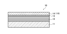
- FIG. 1 is a schematic cross-sectional view showing an example of an embodiment of a reflective mask blank of the present invention.
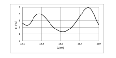
- FIG. 2 shows Example 1 in which the pattern film has a two-layer structure of a TaN film (on the substrate side: film thickness d 2 : 37.0 nm) and a Ru film (on the opposite side to the substrate: film thickness d 1 : 3.3 nm). It is a graph showing the relationship between exposure wavelength ⁇ and reflectance R for a reflective mask blank.
- FIG. 2 shows Example 1 in which the pattern film has a two-layer structure of a TaN film (on the substrate side: film thickness d 2 : 37.0 nm) and a Ru film (on the opposite side to the substrate: film thickness d 1 : 3.3 nm). It is a graph showing the relationship between exposure wavelength ⁇ and reflectance R for a reflective mask blank.
- FIG. 1 is a schematic cross-sectional view showing an example of an embodiment of a reflective mask blank of the present invention.
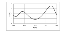
- Example 2 shows Example 2 in which the pattern film has a two-layer structure of a TaN film (on the substrate side: film thickness d 2 : 44.0 nm) and a Ru film (on the opposite side to the substrate: film thickness d 1 : 3.8 nm). It is a graph showing the relationship between exposure wavelength ⁇ and reflectance R for a reflective mask blank.
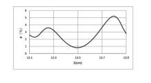
- the pattern films are a TaN film (substrate side: film thickness d 3 : 32.6 nm), a SiN film (film thickness d 2 : 2.6 nm), and a TaN film (on the side opposite to the substrate: film thickness d 1 : 4).
- FIG. 5 is a graph showing the relationship between the exposure wavelength ⁇ and the reflectance R for the reflective mask blank of Example 3 having a three-layer structure.
- FIG. 5 shows Example 4 in which the pattern film has a two-layer structure of a TaN film (on the substrate side: film thickness d 2 : 28.4 nm) and a Pt film (on the opposite side to the substrate: film thickness d 1 : 12.1 nm). It is a graph showing the relationship between exposure wavelength ⁇ and reflectance R for a reflective mask blank.
- FIG. 5 shows Example 4 in which the pattern film has a two-layer structure of a TaN film (on the substrate side: film thickness d 2 : 28.4 nm) and a Pt film (on the opposite side to the substrate: film thickness d 1 : 12.1 nm). It is a graph showing the relationship between exposure wavelength ⁇ and reflectance R for a reflective mask blank.
- FIG. 5 shows Example 4 in which the pattern film has a two-layer structure of
- Example 6 shows Example 5 in which the pattern film has a two-layer structure of a TaN film (on the substrate side: film thickness d 2 : 27.3 nm) and a Pt film (on the opposite side to the substrate: film thickness d 1 : 13.4 nm). It is a graph showing the relationship between exposure wavelength ⁇ and reflectance R for a reflective mask blank.
- FIG. 7 shows Example 6 in which the pattern film has a two-layer structure of a TaN film (on the substrate side: film thickness d 2 : 28.2 nm) and a Pt film (on the opposite side to the substrate: film thickness d 1 : 12.4 nm). It is a graph showing the relationship between exposure wavelength ⁇ and reflectance R for a reflective mask blank.
- FIG. 7 shows Example 6 in which the pattern film has a two-layer structure of a TaN film (on the substrate side: film thickness d 2 : 28.2 nm) and a Pt film (on the opposite side to the substrate: film
- Example 7 shows Example 7 in which the pattern film has a two-layer structure of a Cr film (on the substrate side: film thickness d 2 : 38.0 nm) and a Ru film (on the opposite side to the substrate: film thickness d 1 : 2.8 nm). It is a graph showing the relationship between exposure wavelength ⁇ and reflectance R for a reflective mask blank.
- the pattern films are a Cr film (substrate side: film thickness d 3 :33.1 nm), a Si film (film thickness d 2 :3.1 nm), and a Cr film (on the opposite side to the substrate: film thickness d 1 :3).
- FIG. 9 is a graph showing the relationship between the exposure wavelength ⁇ and the reflectance R for the reflective mask blank of Example 8, which has a three-layer structure with .9 nm).
- FIG. 10 shows Example 9 in which the pattern film has a two-layer structure of a SnO 2 film (on the substrate side: film thickness d 2 : 24.1 nm) and a Ru film (on the side opposite to the substrate: film thickness d 1 : 2.2 nm).
- 3 is a graph showing the relationship between the exposure wavelength ⁇ and the reflectance R for the reflective mask blank of FIG.
- any of the preferable ones can be adopted, and combinations of the preferable ones can be said to be more preferable.
- the expression "XX to YY” means “XX to YY”.
- “exp(t)” means “e t ".
- the lower and upper limits described in stages for preferred numerical ranges may be independently combined. For example, from the description "preferably 10 to 90, more preferably 30 to 60", the “preferable lower limit (10)” and “more preferable upper limit (60)” are combined to become “10 to 60". You can also do that.
- the upper limit or lower limit of the numerical range may be replaced with the value shown in the Examples.
- the reflective mask blank of this embodiment includes a substrate, a multilayer reflective film that reflects EUV light, and a pattern film in this order, and further includes other layers such as a protective film, if necessary.
- the pattern film is a layer that is partially etched during mask processing, and includes an absorber film.
- the pattern film may include a buffer layer, a low reflection layer, etc. in addition to the absorber film.
- the multilayer reflective film reflects EUV light in the openings where no absorber film is present, and the pattern film reduces the reflection of EUV light in the non-openings where the absorber film exists. It is of binary type.
- FIG. 1 is a schematic cross-sectional view showing an example of an embodiment of a reflective mask blank of the present invention.
- a multilayer reflective film 12, a protective film 13, and an absorber film 14 as a pattern film 15 are formed on a substrate 11 in this order.
- the substrate 11 satisfies the characteristics as a substrate for an EUV mask blank. Therefore, the substrate 11 has a low coefficient of thermal expansion (specifically, a coefficient of thermal expansion at 20°C of preferably 0 ⁇ 0.05 ⁇ 10 ⁇ 7 /°C, more preferably 0 ⁇ 0.03 ⁇ 10 ⁇ 7 /°C). °C), and has excellent smoothness, flatness, and resistance to cleaning liquids used for cleaning mask blanks or photomasks after pattern formation.
- the substrate 11 is made of glass having a low coefficient of thermal expansion, such as SiO 2 -TiO 2 glass, but is not limited to this, and may be made of crystallized glass with ⁇ -quartz solid solution precipitated, quartz glass, silicon, etc. A substrate made of metal or the like can also be used.
- the substrate 11 has a smooth surface with a surface roughness (rms) of 0.15 nm or less and a flatness of 100 nm or less because high reflectance and transfer accuracy can be obtained in the photomask after pattern formation.
- rms surface roughness
- the size, thickness, etc. of the substrate 11 are appropriately determined based on the design values of the mask, etc. It is preferable that there be no defects on the surface of the substrate 11 on which the multilayer reflective film 12 is formed. However, even if a defect exists, it is sufficient that no phase defect occurs due to a concave defect and/or a convex defect. Specifically, it is preferable that the depth of the concave defect and the height of the convex defect be 2 nm or less, and that the half width of the concave defect and the convex defect be 60 nm or less.
- the half-width of a concave defect refers to the width at 1/2 the depth of the concave defect.
- the half-width of a convex defect refers to the width at a position half the height of the convex defect.
- the multilayer reflective film 12 reflects EUV light and achieves high EUV light reflectance by alternately stacking high refractive index layers and low refractive index layers multiple times.
- Mo is widely used for the high refractive index layer
- Si is widely used for the low refractive index layer. That is, Mo/Si multilayer reflective film is the most common.
- the multilayer reflective film 12 is not particularly limited as long as it has the desired characteristics as a reflective layer of a reflective mask blank.
- the characteristic particularly required of the multilayer reflective film 12 is high EUV light reflectance.
- the peak reflectance of the light in the EUV wavelength region i.e., the light reflectance around the wavelength of 13.5 nm
- peak reflectance of EUV light is preferably 60% or more, more preferably 65% or more.
- the peak reflectance of EUV light is preferably 60% or more, more preferably 65% or more.
- each layer constituting the multilayer reflective film 12 and the number of repeating units of the layers can be appropriately selected depending on the film material used and the EUV light reflectance required of the reflective layer.
- the multilayer reflective film in order to make the multilayer reflective film 12 with a maximum value of EUV light reflectance of 60% or more, the multilayer reflective film should be made of Mo with a film thickness of 2.3 nm ⁇ 0.1 nm.
- This layer and a Si layer having a film thickness of 4.5 nm ⁇ 0.1 nm may be laminated so that the number of repeating units is 30 to 60.
- the thickness of the multilayer reflective film 12 can be measured, for example, using a transmission electron microscope (TEM) on a cross section taken along the thickness direction (Z direction) of the reflective mask blank.
- TEM transmission electron microscope
- the uppermost layer of the multilayer reflective film 12 is preferably made of a material that is not easily oxidized.
- the layer of material that is not easily oxidized functions as a cap layer for the multilayer reflective film 12.
- a specific example of a layer of oxidizable material that functions as a cap layer is a Si layer.
- the uppermost layer functions as a cap layer by making the uppermost layer a Si layer.
- the thickness of the cap layer is preferably 11 ⁇ 2 nm.
- the thickness of the cap layer can be measured, for example, using a transmission electron microscope (TEM) on a cross section taken along the thickness direction (Z direction) of the reflective mask blank.
- TEM transmission electron microscope
- the protective film 13 is provided for the purpose of protecting the multilayer reflective film 12 so that the multilayer reflective film 12 is not damaged by the etching process when the absorber film 14 is patterned by an etching process, usually a dry etching process. Any layer. Therefore, as the material for the protective film 13, a material is selected that is not easily affected by the etching process of the absorber film 14, that is, its etching rate is slower than that of the absorber film 14, and it is also less likely to be damaged by this etching process. . In order to satisfy the above characteristics, the protective film 13 preferably contains at least one of Rh and Ru (Ru alloy, Rh alloy, etc.).
- the above-mentioned materials include Ru metal alone, Ru alloy containing Ru and one or more metals selected from the group consisting of Si, Ti, Nb, Mo, Rh, and Zr, and Rh metal alone, Rh alloy containing Rh and one or more metals selected from the group consisting of Si, Ti, Nb, Mo, Ru, Ta, and Zr, Rh containing containing the above Rh alloy and N
- Rh-based materials such as nitrides and Rh-containing oxynitrides containing the Rh alloy, N, and O.
- examples of materials that can achieve the above object include Al, nitrides containing these metals and N, and Al 2 O 3 .
- materials that can achieve the above object are preferably Ru metal alone, Ru alloy, Rh metal alone, or Rh alloy.
- the Ru alloy is preferably a Ru--Si alloy or a Ru--Rh alloy
- the Rh alloy is preferably a Rh--Si alloy or a Rh--Ru alloy.
- the thickness of the protective film 13 is preferably 1 to 10 nm, more preferably 1 to 5 nm.
- the thickness of the protective film 13 can be measured, for example, using a transmission electron microscope (TEM) on a cross section taken along the thickness direction (Z direction) of the reflective mask blank.
- TEM transmission electron microscope
- the protective film may be a film consisting of a single layer or a multilayer film consisting of multiple layers.
- each layer constituting the multilayer film is preferably made of the above-mentioned preferred material.
- the protective film is a multilayer film, it is also preferable that the total film thickness of the multilayer film falls within the above-mentioned preferable range.
- the protective film can be formed using a known film forming method such as a magnetron sputtering method or an ion beam sputtering method.
- a known film forming method such as a magnetron sputtering method or an ion beam sputtering method.
- an Ru target as a target and Ar gas as a sputtering gas.
- a particularly required characteristic of the binary absorber film 14 is extremely low EUV light reflectance.
- the peak reflectance of EUV light when the surface of the absorber film 14 is irradiated with light in the wavelength range of EUV light is preferably 1.3% or less, more preferably 1% or less. , more preferably 0.98% or less, particularly preferably 0.50% or less, most preferably 0.30% or less.
- the reflectance of the absorber film 14 can be measured using, for example, an EUV reflectance meter.
- the absorber film 14 is made of a material with a high absorption coefficient for EUV light.
- a material containing tantalum (Ta) as a main component is preferable.
- a material containing tantalum (Ta) as a main component means a material containing 20 at% or more of Ta.
- Materials containing Ta as a main component used for the absorber film 14 include, in addition to Ta, hafnium (Hf), Si, zirconium (Zr), germanium (Ge), boron (B), palladium (Pd), tin (Sn), Chromium (Cr), manganese (Mn), iron (Fe), cobalt (Co), silver (Ag), cadmium (Cd), indium (In), antimony (Sb), tungsten (W), rhenium (Re), Osmium (Os), iridium (Ir), platinum (Pt), gold (Au), thallium (Tl), lead (Pb), bismuth (Bi), carbon (C), titanium (Ti), zirconium (Zr), Mo, Ru, rhodium (Rh), palladium (Pd), calcium (Ca), magnesium (Mg), Al, nickel (Ni), copper (Cu), zinc (Zn), gallium (Ga), arsenic (As) ,
- materials containing the above elements other than Ta include, for example, TaN, TaNH, TaHf, TaHfN, TaBSi, TaBSiN, TaB, TaBN, TaSi, TaSiN, TaGe, TaGeN, TaZr, TaZrN, TaPd, TaSn, TaPdN. , TaSn, TaCr, TaMn, TaFe, TaCo, TaAg, TaCd, TaIn, TaSb, TaW, and the like.
- the thickness of the absorber film 14 is preferably 20 to 90 nm.
- the thickness of the absorber film 14 can be measured, for example, using a transmission electron microscope (TEM) on a cross section taken along the thickness direction (Z direction) of the reflective mask blank.
- TEM transmission electron microscope
- the pattern film including the above-mentioned absorber film has a laminated structure having a total of L layers (where L is a natural number of 2 or more) having different refractive indexes.
- L is not particularly limited as long as it is a natural number of 2 or more, but is preferably 8 or less, more preferably 6 or less, and even more preferably 5 or less. That is, L is, for example, 2 to 8.
- Examples of patterned films include "a two-layer structure of a TaN film (on the substrate side) and a Pt film (on the opposite side to the substrate)" and "a two-layer structure of a Cr film (on the substrate side) and a Ru film (on the opposite side to the substrate)".
- the refractive index of the i-th layer (i is a natural number) from the side opposite to the substrate in the pattern film is n i
- the refractive index of the i-th layer from the side opposite to the substrate in the pattern film is n i.
- the absorption coefficient is k i , the thickness of the i-th layer from the side opposite to the substrate in the pattern film is di (nm), the total thickness of the pattern film is d, the exposure wavelength is ⁇ (nm),
- P i is 1-exp (-2 ⁇ / ⁇ *d i k i )
- the following formula (1) is satisfied and the following formula (1-1) is satisfied, and the following formula (1-2) is It is more preferable to satisfy.
- the refractive index n i and the absorption coefficient k i are values at a wavelength of 13.5 nm, for example.
- the reflection amplitude of the i-th layer from the side opposite to the substrate in the patterned film is r i
- the following formula (2 -1) is more preferable, and it is particularly preferable to satisfy the following formula (2-2).
- the reflection amplitude r L of the L-th layer from the side opposite to the substrate in the pattern film is calculated as
- the refractive index n1 of the first outermost layer from the side opposite to the substrate in the pattern film is not particularly limited, but from the viewpoint of generating reflection amplitude at the interface with vacuum, it is preferably 0.950 or less, more preferably is 0.945 or less, particularly preferably 0.940 or less, and is preferably 0.830 or more, more preferably from the viewpoint of utilizing the cancellation of reflected waves due to the reflection amplitude between the outermost layer and the second layer material. is 0.860 or more, particularly preferably 0.870 or more.
- the refractive index n 1 and film thickness d 1 of the first outermost layer from the side opposite to the substrate in the pattern film satisfy the following formula (3), and more preferably satisfy the following formula (3-1). , it is particularly preferable that formula (3-2) be satisfied.
- x is an integer of 0 or more.
- between the absorption coefficients k of two adjacent layers in the pattern film is preferably 0.0200 from the viewpoint of utilizing the cancellation of reflected waves.
- the above value is more preferably 0.0210 or more, particularly preferably 0.0220 or more.
- is preferably 0.0700 or less, more preferably 0.0600 or less, particularly preferably 0.0550 or less.
- the reflectance of the pattern film is not particularly limited as long as it is sufficiently reduced, but it is preferably 1.3% or less, more preferably 1% or less, and still more preferably 0.98% or less. It is particularly preferably 0.50% or less, most preferably 0.30% or less. Note that the reflectance of the patterned film can be measured with an EUV reflectance meter, and an optical multilayer film simulation can be performed.
- the total thickness d of the pattern film is not particularly limited as long as it is sufficiently reduced, but is preferably 45 nm or less, more preferably 43 nm or less, still more preferably 42 nm or less, and particularly preferably It is 41 nm or less.
- the total film thickness of the pattern film can be measured, for example, using a transmission electron microscope (TEM) on a cross section taken along the thickness direction (Z direction) of the reflective mask blank.
- TEM transmission electron microscope
- a buffer layer may be formed between the protective film 13 and the absorber film 14.
- the buffer layer is a layer that protects the multilayer reflective film during dry etching and defect correction.
- the material for the buffer layer is not particularly limited, and examples thereof include SiO 2 , CrN, and the like.
- a low reflective layer may be formed on the absorber film 14.
- the low-reflection layer is composed of a film that exhibits low reflection in the inspection light used to inspect the mask pattern.
- a pattern is formed on the absorber film and then inspected to see if the pattern is formed as designed.
- an inspection machine that uses light of approximately 193 nm or 257 nm as inspection light is used.
- the difference in the reflectance of light of about 193 nm and 257 nm, specifically, the difference between the exposed surface of the absorber film removed by patterning and the surface of the absorber film that remained without being removed by patterning.
- the former is the surface of the protective film. Therefore, if the difference in reflectance between the surface of the protective film and the surface of the absorber film with respect to the wavelength of the test light is small, the contrast during the test will be poor and accurate testing will not be possible. If the difference in reflectance between the protective film surface and the absorber film surface with respect to the wavelength of the inspection light is small, the contrast during inspection will be good due to the formation of the low reflection layer.
- the material for the low reflection layer is not particularly limited, and examples include tantalum oxynitride. Since the low reflection layer corresponds to the first outermost layer from the side opposite to the substrate in the patterned film, it is preferable that formula (3) is satisfied.
- the reflective mask of this embodiment has a pattern obtained by patterning the pattern film in the reflective mask blank of the present invention. That is, the reflective mask of this embodiment includes, in this order, a substrate, a multilayer reflective film that reflects EUV light, and a pattern in which the patterned film is patterned, and, if necessary, other layers such as a protective film. Be prepared for more. Layers other than the pattern (other layers such as the substrate, multilayer reflective film, and protective film) are as described for the reflective mask blank. The pattern will be explained in "Method for manufacturing reflective mask" below.
- a pattern film in the reflective mask blank of this embodiment is patterned. That is, the reflective mask of this embodiment can be manufactured using the reflective mask blank of this embodiment described above.
- a photolithography method that can perform high-definition patterning is most suitable.
- a resist film (not shown) is formed on the outermost surface of the reflective mask blank 10 shown in FIG. 1 (the absorber film 14 which is the uppermost layer of the pattern film 15).
- the thickness of the resist film can be, for example, 100 nm.
- a desired pattern is drawn (exposed) on this resist film, and further developed and rinsed to form a predetermined resist pattern (not shown).
- the pattern film 15 (absorber film 14) is dry etched using an etching gas containing a fluorine gas such as SF 6 using a resist pattern (not shown) as a mask. form). After pattern formation, the resist pattern (not shown) is removed.
- the etching rate of the pattern film 15 depends on the material forming the pattern film 15 (absorber film 14) and conditions such as the etching gas. Since the pattern film 15 (absorber film 14) is composed of a multilayer film made of different materials, conditions such as etching rate and etching gas may change for each layer of different materials.
- a pattern is formed by the above. If the pattern film 15 (absorber film 14) made of a multilayer film can be continuously etched by dry etching using one type of etching gas, the effect of process simplification can be obtained. Next, wet cleaning is performed using an acidic or alkaline aqueous solution to obtain a reflective mask for EUV lithography that achieves high reflectance.
- etching gases include CHF 3 , CF 4 , C 2 F 6 , C 3 F 6 , C 4 F 6 , C 4 F 8 , CH 2 F 2 , CH 3 F, and C 3 F.
- a fluorine-based gas such as 8 and F, and a mixed gas containing these fluorine gases and O 2 in a predetermined ratio can be used.
- other gases may be used as long as they are useful for processing.
- gases include, for example, chlorine-based gases such as Cl 2 , SiCl 4 , CHCl 3 , CCl 4 , BCl 3 and mixed gases thereof, mixed gases containing chlorine-based gas and He in a predetermined ratio, and chlorine-based gases. and a mixed gas containing Ar in a predetermined proportion, a halogen gas containing at least one selected from fluorine gas, chlorine gas, bromine gas, and iodine gas, and at least one type selected from the group consisting of hydrogen halide gas, or There are many more. Further examples include mixed gases containing these gases and oxygen gas.
- a binary reflective mask blank comprising a substrate, a multilayer reflective film that reflects EUV light, and a pattern film in this order, the pattern film having a total of L layers each having a different refractive index.
- It has a laminated structure (L is a natural number of 2 or more), and the absorption coefficient of the i-th layer from the side opposite to the substrate in the pattern film is k i , and The thickness of the i-th layer is d i (nm), the total thickness of the pattern film is d, the exposure wavelength is ⁇ (nm), and P i is 1-exp(-2 ⁇ / ⁇ *d i k i ), a reflective mask blank that satisfies the following formula (1).
- ⁇ 3> The reflective mask blank according to ⁇ 1> or ⁇ 2> above, wherein the first outermost layer of the patterned film from the side opposite to the substrate has a refractive index n 1 of 0.950 or less.
- n 1 refractive index
- ⁇ 4> The reflective mask according to any one of ⁇ 1> to ⁇ 3> above, wherein at least one of the differences
- ⁇ 5> The refractive index of the i-th layer from the side opposite to the substrate in the pattern film is n i , and the film thickness d 1 of the first outermost layer from the side opposite to the substrate in the pattern film is expressed by the following formula:
- x is an integer greater than or equal to 0.
- ⁇ 6> The reflective mask blank according to any one of ⁇ 1> to ⁇ 5> above, wherein the pattern film has a reflectance of 1.3% or less.
- ⁇ 7> The reflective mask blank according to any one of ⁇ 1> to ⁇ 6> above, wherein the pattern film has a reflectance of 1% or less.
- ⁇ 8> The reflective mask blank according to any one of ⁇ 1> to ⁇ 7> above, wherein the total film thickness d of the pattern film is 45 nm or less.
- ⁇ 9> The reflective mask blank according to any one of ⁇ 1> to ⁇ 8> above, further comprising a protective film between the multilayer reflective film and the pattern film.
- a reflective mask wherein the pattern film in the reflective mask blank according to any one of ⁇ 1> to ⁇ 9> above has a patterned pattern.
- ⁇ 11> A method for manufacturing a reflective mask, comprising patterning the pattern film in the reflective mask blank according to any one of ⁇ 1> to ⁇ 9> above.
- Examples 1 to 3 are comparative examples, and Examples 4 to 9 are examples.
- the reflective mask blank of Example 1 includes a substrate, a multilayer reflective film formed on the substrate, a protective film formed on the multilayer reflective film, and an absorber film as a pattern film formed on the protective film. Equipped with A SiO 2 -TiO 2 glass substrate (thickness: 6.3 mm) was selected as the substrate, and a silicon film (thickness: 4.5 nm) and a molybdenum film (thickness: 2.3 nm) were alternately repeated in the number of units.
- a laminated structure in which (thickness d 2 : 37.0 nm) and a ruthenium (Ru) film (thickness d 1 : 3.3 nm), a patterned film (absorber film) (patterned film thickness d :40.3nm).
- the absorber film on the substrate side is a tantalum nitride (TaN) film
- the absorber film on the opposite side to the substrate is a ruthenium (Ru) film.
- the left side of equation (1) 0.0109
- the left side of equation (2) 0.094
- Example 2 shows Example 1 in which the pattern film has a two-layer structure of a TaN film (on the substrate side: film thickness d 2 : 37.0 nm) and a Ru film (on the opposite side to the substrate: film thickness d 1 : 3.3 nm). It is a graph showing the relationship between exposure wavelength ⁇ and reflectance R for a reflective mask blank. The reflectance of the patterned film at a wavelength of 13.5 nm was 2.62% (Table 1). FIG. 2 was obtained by performing an optical multilayer film simulation.
- Example 2 In Example 1, a patterned film (absorbing Instead of selecting a tantalum nitride (TaN) film (film thickness d 2 : 44.0 nm) and a ruthenium (Ru) film (film thickness d 1 :3) (pattern film thickness d: 40.3 nm).
- the left side of equation (2) 0.094
- FIG. 1 a patterned film (absorbing Instead of selecting a tantalum nitride (TaN) film (film thickness d 2 : 44.0 nm) and a ruthenium (Ru) film (film thickness d 1 :3) (pattern film thickness
- Example 3 shows Example 2 in which the pattern film has a two-layer structure of a TaN film (on the substrate side: film thickness d 2 : 44.0 nm) and a Ru film (on the opposite side to the substrate: film thickness d 1 : 3.8 nm). It is a graph showing the relationship between exposure wavelength ⁇ and reflectance R for a reflective mask blank. The reflectance of the patterned film at a wavelength of 13.5 nm was 1.36% (Table 1). FIG. 3 was obtained by performing an optical multilayer film simulation.
- the pattern films are a TaN film (substrate side: film thickness d 3 : 32.6 nm), a SiN film (film thickness d 2 : 2.6 nm), and a TaN film (on the side opposite to the substrate: film thickness d 1 : 4).
- FIG. 5 nm is a graph showing the relationship between the exposure wavelength ⁇ and the reflectance R for the reflective mask blank of Example 3 having a three-layer structure.
- the reflectance of the patterned film at a wavelength of 13.5 nm was 4.01% (Table 1).
- FIG. 4 was obtained by performing an optical multilayer film simulation.
- FIG. 5 shows Example 4 in which the pattern film has a two-layer structure of a TaN film (on the substrate side: film thickness d 2 : 28.4 nm) and a Pt film (on the opposite side to the substrate: film thickness d 1 : 12.1 nm). It is a graph showing the relationship between exposure wavelength ⁇ and reflectance R for a reflective mask blank. The reflectance of the patterned film at a wavelength of 13.5 nm was 0.84% (Table 1). FIG. 5 was obtained by performing an optical multilayer film simulation.
- Example 5 shows Example 5 in which the pattern film has a two-layer structure of a TaN film (on the substrate side: film thickness d 2 : 27.3 nm) and a Pt film (on the opposite side to the substrate: film thickness d 1 : 13.4 nm). It is a graph showing the relationship between exposure wavelength ⁇ and reflectance R for a reflective mask blank. The reflectance of the patterned film at a wavelength of 13.5 nm was 0.94% (Table 1). FIG. 6 was obtained by performing an optical multilayer film simulation.
- Example 7 shows Example 6 in which the pattern film has a two-layer structure of a TaN film (on the substrate side: film thickness d 2 : 28.2 nm) and a Pt film (on the opposite side to the substrate: film thickness d 1 : 12.4 nm). It is a graph showing the relationship between exposure wavelength ⁇ and reflectance R for a reflective mask blank. The reflectance of the patterned film at a wavelength of 13.5 nm was 0.85% (Table 1). FIG. 7 was obtained by performing an optical multilayer film simulation.
- FIG. 8 shows a reflective type of Example 7 in which the pattern film has a two-layer structure of a Cr film (on the substrate side: film thickness d 2 : 38 nm) and a Ru film (on the opposite side to the substrate: film thickness d 1 : 2.8 nm). It is a graph showing the relationship between exposure wavelength ⁇ and reflectance R for a mask blank. The reflectance of the patterned film at a wavelength of 13.5 nm was 0.95% (Table 1). FIG. 8 was obtained by performing an optical multilayer film simulation.
- the pattern films are a Cr film (substrate side: film thickness d 3 :33.1 nm), a Si film (film thickness d 2 :3.1 nm), and a Cr film (on the opposite side to the substrate: film thickness d 1 :3).
- 9 is a graph showing the relationship between the exposure wavelength ⁇ and the reflectance R for the reflective mask blank of Example 8, which has a three-layer structure with .9 nm). The reflectance of the patterned film at a wavelength of 13.5 nm was 0.82% (Table 1).
- FIG. 9 was obtained by performing an optical multilayer film simulation.
- Example 10 shows Example 9 in which the pattern film has a two-layer structure of a SnO 2 film (on the substrate side: film thickness d 2 : 24.1 nm) and a Ru film (on the opposite side to the substrate: film thickness d 1 : 2.8 nm).
- FIG. 3 is a graph showing the relationship between the exposure wavelength ⁇ and the reflectance R for the reflective mask blank of FIG.
- the reflectance of the patterned film at a wavelength of 13.5 nm was 0.29% (Table 1).
- FIG. 10 was obtained by performing an optical multilayer film simulation.
- the reflective mask blanks (Examples 4 to 9) that satisfy formula (1) can sufficiently reduce the reflectance of the pattern film while reducing the thickness of the pattern film (reflectance: 0.29
- reflective mask blanks that do not satisfy formula (1) (Examples 1 to 3) cannot sufficiently reduce the reflectance of the pattern film (reflectance: 1.36 to 4). .01%).
Landscapes
- Physics & Mathematics (AREA)
- General Physics & Mathematics (AREA)
- Preparing Plates And Mask In Photomechanical Process (AREA)
- Exposure Of Semiconductors, Excluding Electron Or Ion Beam Exposure (AREA)
Abstract
Priority Applications (2)
| Application Number | Priority Date | Filing Date | Title |
|---|---|---|---|
| JP2024506294A JPWO2023171583A1 (fr) | 2022-03-08 | 2023-03-03 | |
| KR1020247029740A KR20240136468A (ko) | 2022-03-08 | 2023-03-03 | 반사형 마스크 블랭크 그리고 반사형 마스크 및 그 제조 방법 |
Applications Claiming Priority (2)
| Application Number | Priority Date | Filing Date | Title |
|---|---|---|---|
| JP2022035462 | 2022-03-08 | ||
| JP2022-035462 | 2022-03-08 |
Publications (1)
| Publication Number | Publication Date |
|---|---|
| WO2023171583A1 true WO2023171583A1 (fr) | 2023-09-14 |
Family
ID=87934975
Family Applications (1)
| Application Number | Title | Priority Date | Filing Date |
|---|---|---|---|
| PCT/JP2023/008186 WO2023171583A1 (fr) | 2022-03-08 | 2023-03-03 | Substrat pour masque réflecteur, masque réflecteur et procédé de fabrication associé |
Country Status (4)
| Country | Link |
|---|---|
| JP (1) | JPWO2023171583A1 (fr) |
| KR (1) | KR20240136468A (fr) |
| TW (1) | TW202336520A (fr) |
| WO (1) | WO2023171583A1 (fr) |
Citations (4)
| Publication number | Priority date | Publication date | Assignee | Title |
|---|---|---|---|---|
| JP2018169617A (ja) * | 2013-09-27 | 2018-11-01 | Hoya株式会社 | マスクブランク用基板、多層反射膜付き基板、反射型マスクブランク、反射型マスク及び半導体装置の製造方法 |
| JP2018180544A (ja) * | 2017-04-17 | 2018-11-15 | Agc株式会社 | Euv露光用反射型マスクブランク、および反射型マスク |
| US20190146325A1 (en) * | 2017-11-14 | 2019-05-16 | Taiwan Semiconductor Manufacturing Co., Ltd. | Extreme ultraviolet mask with reduced wafer neighboring effect and method of manufacturing the same |
| JP2022505688A (ja) * | 2018-10-26 | 2022-01-14 | アプライド マテリアルズ インコーポレイテッド | 裏側コーティングを有する極紫外線マスク |
Family Cites Families (1)
| Publication number | Priority date | Publication date | Assignee | Title |
|---|---|---|---|---|
| JP6408790B2 (ja) | 2013-05-31 | 2018-10-17 | Hoya株式会社 | 反射型マスクブランク、反射型マスク及びその製造方法、並びに半導体装置の製造方法 |
-
2023
- 2023-03-03 WO PCT/JP2023/008186 patent/WO2023171583A1/fr active Application Filing
- 2023-03-03 KR KR1020247029740A patent/KR20240136468A/ko active Search and Examination
- 2023-03-03 JP JP2024506294A patent/JPWO2023171583A1/ja active Pending
- 2023-03-08 TW TW112108478A patent/TW202336520A/zh unknown
Patent Citations (4)
| Publication number | Priority date | Publication date | Assignee | Title |
|---|---|---|---|---|
| JP2018169617A (ja) * | 2013-09-27 | 2018-11-01 | Hoya株式会社 | マスクブランク用基板、多層反射膜付き基板、反射型マスクブランク、反射型マスク及び半導体装置の製造方法 |
| JP2018180544A (ja) * | 2017-04-17 | 2018-11-15 | Agc株式会社 | Euv露光用反射型マスクブランク、および反射型マスク |
| US20190146325A1 (en) * | 2017-11-14 | 2019-05-16 | Taiwan Semiconductor Manufacturing Co., Ltd. | Extreme ultraviolet mask with reduced wafer neighboring effect and method of manufacturing the same |
| JP2022505688A (ja) * | 2018-10-26 | 2022-01-14 | アプライド マテリアルズ インコーポレイテッド | 裏側コーティングを有する極紫外線マスク |
Also Published As
| Publication number | Publication date |
|---|---|
| TW202336520A (zh) | 2023-09-16 |
| KR20240136468A (ko) | 2024-09-13 |
| JPWO2023171583A1 (fr) | 2023-09-14 |
Similar Documents
| Publication | Publication Date | Title |
|---|---|---|
| TWI730071B (zh) | 反射型遮罩基底、反射型遮罩及半導體裝置之製造方法 | |
| TW201842208A (zh) | 反射型光罩基底、反射型光罩及其製造方法、與半導體裝置之製造方法 | |
| JP7475154B2 (ja) | 反射型マスクブランク、反射型マスク、導電膜付き基板、及び半導体装置の製造方法 | |
| WO2022138360A1 (fr) | Ébauche de masque réfléchissant, masque réfléchissant et procédé de fabrication de dispositif semi-conducteur | |
| WO2020184473A1 (fr) | Ébauche de masque de type réflexion, masque de type réflexion et procédé pour le fabriquer, et procédé de fabrication de dispositif à semi-conducteur | |
| CN112666788A (zh) | 带多层反射膜的基板、反射型掩模坯料、反射型掩模及制造方法、及半导体装置制造方法 | |
| KR20210088582A (ko) | 반사형 포토마스크 블랭크 및 반사형 포토마스크 | |
| KR102511751B1 (ko) | 극자외선 리소그래피용 블랭크마스크 및 포토마스크 | |
| WO2020045029A1 (fr) | Ébauche de masque réfléchissant, masque réfléchissant et procédé de fabrication associé, et procédé de fabrication de dispositif à semi-conducteur | |
| KR20200088283A (ko) | 반사형 마스크 블랭크, 반사형 마스크 및 그 제조 방법, 및 반도체 장치의 제조 방법 | |
| TW202117439A (zh) | 附多層反射膜之基板、反射型光罩基底、反射型光罩、及半導體裝置之製造方法 | |
| JPWO2019102990A1 (ja) | マスクブランク、位相シフトマスクおよび半導体デバイスの製造方法 | |
| TW202038001A (zh) | 反射型光罩基底、反射型光罩及其製造方法、與半導體裝置之製造方法 | |
| JP2020034666A5 (fr) | ||
| JP6968945B2 (ja) | 反射型マスクブランク、反射型マスク及び半導体装置の製造方法 | |
| WO2022172916A1 (fr) | Ébauche de masque photographique réfléchissant et masque photographique réfléchissant | |
| WO2023171583A1 (fr) | Substrat pour masque réflecteur, masque réflecteur et procédé de fabrication associé | |
| JP5018212B2 (ja) | 反射型フォトマスクブランク及び反射型フォトマスク並びに半導体装置の製造方法 | |
| JP7121814B2 (ja) | マスクブランク、転写用マスク、マスクブランクの製造方法 | |
| JP2020042208A (ja) | マスクブランク、転写用マスクおよび半導体デバイスの製造方法 | |
| KR20230119119A (ko) | 반사형 마스크 블랭크, 반사형 마스크, 반사형 마스크의 제조 방법 및 반도체 디바이스의 제조 방법 | |
| JP7066881B2 (ja) | マスクブランク、位相シフトマスク、位相シフトマスクの製造方法及び半導体デバイスの製造方法 | |
| TW202238252A (zh) | 反射型空白光罩及反射型光罩 | |
| TW202038002A (zh) | 遮罩基底、相移遮罩、相移遮罩之製造方法及半導體元件之製造方法 | |
| US20240329515A1 (en) | Blankmask for euv lithography with absorbing film, and photomask fabricated with the same |
Legal Events
| Date | Code | Title | Description |
|---|---|---|---|
| 121 | Ep: the epo has been informed by wipo that ep was designated in this application |
Ref document number: 23766759 Country of ref document: EP Kind code of ref document: A1 |
|
| ENP | Entry into the national phase |
Ref document number: 2024506294 Country of ref document: JP Kind code of ref document: A |
|
| ENP | Entry into the national phase |
Ref document number: 20247029740 Country of ref document: KR Kind code of ref document: A |
|
| WWE | Wipo information: entry into national phase |
Ref document number: 1020247029740 Country of ref document: KR |