WO2023171412A1 - 設計支援装置、および学習装置 - Google Patents
設計支援装置、および学習装置 Download PDFInfo
- Publication number
- WO2023171412A1 WO2023171412A1 PCT/JP2023/006699 JP2023006699W WO2023171412A1 WO 2023171412 A1 WO2023171412 A1 WO 2023171412A1 JP 2023006699 W JP2023006699 W JP 2023006699W WO 2023171412 A1 WO2023171412 A1 WO 2023171412A1
- Authority
- WO
- WIPO (PCT)
- Prior art keywords
- information
- package
- circuit board
- integrated circuit
- design
- Prior art date
- Legal status (The legal status is an assumption and is not a legal conclusion. Google has not performed a legal analysis and makes no representation as to the accuracy of the status listed.)
- Ceased
Links
Images







Classifications
-
- G—PHYSICS
- G06—COMPUTING OR CALCULATING; COUNTING
- G06F—ELECTRIC DIGITAL DATA PROCESSING
- G06F30/00—Computer-aided design [CAD]
- G06F30/30—Circuit design
- G06F30/39—Circuit design at the physical level
- G06F30/398—Design verification or optimisation, e.g. using design rule check [DRC], layout versus schematics [LVS] or finite element methods [FEM]
-
- G—PHYSICS
- G06—COMPUTING OR CALCULATING; COUNTING
- G06F—ELECTRIC DIGITAL DATA PROCESSING
- G06F30/00—Computer-aided design [CAD]
- G06F30/20—Design optimisation, verification or simulation
- G06F30/27—Design optimisation, verification or simulation using machine learning, e.g. artificial intelligence, neural networks, support vector machines [SVM] or training a model
-
- H—ELECTRICITY
- H05—ELECTRIC TECHNIQUES NOT OTHERWISE PROVIDED FOR
- H05K—PRINTED CIRCUITS; CASINGS OR CONSTRUCTIONAL DETAILS OF ELECTRIC APPARATUS; MANUFACTURE OF ASSEMBLAGES OF ELECTRICAL COMPONENTS
- H05K3/00—Apparatus or processes for manufacturing printed circuits
-
- G—PHYSICS
- G06—COMPUTING OR CALCULATING; COUNTING
- G06F—ELECTRIC DIGITAL DATA PROCESSING
- G06F2115/00—Details relating to the type of the circuit
- G06F2115/12—Printed circuit boards [PCB] or multi-chip modules [MCM]
Definitions
- the present disclosure relates to a design support device and a learning device.
- Patent Document 1 discloses a design support device.
- the design support device performs a design rule check on the design data using geometric calculations, generates image data from the design data in which the portion determined to be an error is centered, and uses artificial intelligence to perform a design rule check on the design data. performs a design rule check, and displays the results of the design rule check.
- Patent Document 1 considers using the above-mentioned configuration to streamline the work of checking whether an error determined by a design rule check is a true error, but does not teach any solution to the above problem. Or not suggested.
- An object of an aspect of the present disclosure is to provide a technique that can perform appropriate design rule checks on components constituting an electronic circuit board.
- a design support device includes a database unit that stores reference information that associates feature information including the shape of components constituting an electronic circuit board with type information of the components, and a design rule check target.
- a data input unit that accepts input of design data of a target electronic circuit board; an extraction unit that extracts feature information including the shape of components constituting the target electronic circuit board by analyzing the design data; a determination unit that determines type information of a component constituting a target electronic circuit board that corresponds to the extracted characteristic information based on the characteristic information and reference information stored in the database unit;
- the present invention includes a generation unit that generates new design data by adding type information added to the design data, and a check execution unit that executes a design rule check on the new design data.
- a learning device includes a data acquisition unit that acquires learning data including feature information including the shapes of components constituting an electronic circuit board and specification information of the electronic circuit board; and a model generation unit that generates a trained model for estimating type information of the components constituting the electronic circuit board from the feature information and specification information.
- a design support device includes a data input unit that receives input of design data of a target electronic circuit board to be subjected to a design rule check, and configures a target electronic circuit board by analyzing the design data.
- the extraction unit extracts feature information including shape information of the component and specification information of the target electronic circuit board, and the trained model estimates the type information of the component from the feature information and specification information. and an estimation unit that estimates type information by inputting the extracted feature information and specification information.
- FIG. 2 is a diagram showing an example of a hardware configuration of a design support device.
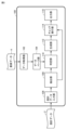
- 1 is a block diagram showing an example of a functional configuration of a design support device according to a first embodiment;
- FIG. It is a figure which shows the symbol figure example of an IC package. It is a figure which shows an example of the information table of an IC package.
- 5 is an updated diagram of the IC package information table of FIG. 4.
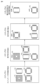
- FIG. FIG. 3 is a diagram for explaining the flow until an IC package name is specified.
- FIG. 3 is a diagram showing an example of a wiring pattern connected to terminals of an IC package.
- FIG. 3 is a diagram showing an example of a wiring pattern information table.
- 9 is an updated diagram of the wiring pattern information table of FIG. 8.
- FIG. 2 is a block diagram showing an example of a functional configuration of a design support device according to a second embodiment.
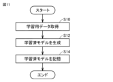
- 3 is a flowchart illustrating an example of learning processing of the design support device.
- 3 is a flowchart illustrating an example of a processing procedure of the design support device.
- FIG. 7 is a diagram showing an example of an information table of an IC package according to another embodiment.
- FIG. 3 is a diagram for explaining the positional relationship between an IC package and peripheral circuit components.
- FIG. 3 is a diagram for explaining a method of applying a threshold value when executing a design rule check.
- the design support apparatus has a function of executing a design rule check on design data (for example, CAD data) of an electronic circuit board (for example, a printed circuit board) on which circuit elements are arranged.
- design data for example, CAD data
- electronic circuit board for example, a printed circuit board
- FIG. 1 is a diagram showing an example of the hardware configuration of the design support apparatus 100.
- the design support device 100 is mainly configured with a microcomputer.
- the design support apparatus 100 includes a processor 150, a main storage device 152, a secondary storage device 154, a communication interface 156, an input device 158, and a display 160. These components are communicatively connected to each other via an internal bus 162.
- the processor 150 is typically an arithmetic processing unit such as a CPU (Central Processing Unit) or an MPU (Multi Processing Unit), and reads various programs including an OS (Operating System) installed in the secondary storage device 154. The program is then expanded to the main storage device 152 and executed.
- arithmetic processing unit such as a CPU (Central Processing Unit) or an MPU (Multi Processing Unit)
- OS Operating System
- the main storage device 152 is typically a volatile storage medium such as DRAM (Dynamic Random Access Memory), and stores the codes of various programs including the OS executed by the processor 150 as well as the codes necessary for executing the various programs. Holds various work data.
- the secondary storage device 154 is a non-volatile storage medium such as a hard disk or an SSD (Solid State Drive), and holds various programs including the OS as well as various setting values.
- Communication interface 156 mediates data transmission between processor 150 and external devices. Communications via communication interface 156 may occur using the Internet, a wide area network (WAN), a local area network (LAN), an Ethernet network, a wired or wireless network, or a combination thereof.
- WAN wide area network
- LAN local area network
- Ethernet Ethernet network
- wired or wireless network or a combination thereof.
- the input device 158 accepts operational input to the design support device.
- the input device 158 is realized by, for example, a keyboard, buttons, a mouse, a touch panel, or the like.
- the display 160 is, for example, a liquid crystal display, an organic EL (Electro Luminescence) display, or the like.
- the display 160 may be configured integrally with the design support apparatus 100 or may be configured separately from the design support apparatus 100.
- circuits such as FPGA (Field Programmable Gate Array) and ASIC (Application Specific Integrated Circuit).
- FIG. 2 is a block diagram showing an example of the functional configuration of the design support apparatus according to the first embodiment.
- the design support apparatus 100 includes a data acquisition section 102, a database section 104, a design data input section 106, an extraction section 108, a determination section 110, a generation section 112, and a check execution section 114. and an output section 116.
- the database unit 104 is realized by the main storage device 152 or the secondary storage device 154.
- each function other than the database unit 104 is realized by the processor 150 executing a program, but may also be realized by a dedicated hardware circuit.
- the data acquisition unit 102 acquires element data 4 regarding each component constituting the electronic circuit board (for example, accepts input of element data 4).
- Element data 4 includes IC-related information regarding the IC included in the electronic circuit board, pattern-related information regarding the wiring pattern on the electronic circuit board, and specification information of the electronic circuit board (for example, product application of the electronic circuit board, amount of current, etc.). (including) and (including).
- the IC related information includes package characteristic information regarding the characteristics of the IC package and package type information indicating the type of the IC package.
- the package characteristic information includes the outline shape of the IC package (for example, the number of sides of the outline), the terminal shape of the IC package (for example, rectangular, circular, etc.), and terminal position information (for example, the relationship between the package outline and the terminals). (information indicating positional relationships), etc.
- the package type information includes, for example, the name of the IC package such as BGA (Ball Grid Array), QFN (Quad Flat Non-leaded package), SOP (Small Outline Package), and QFP (Quad Flat Package).
- the pattern related information includes pattern feature information indicating the characteristics of the wiring pattern and pattern type information indicating the type of the wiring pattern.
- the pattern characteristic information includes the material of the wiring pattern, the dielectric constant of the circuit board on which the wiring pattern is provided, the layer structure of the circuit board, the impedance value of the wiring pattern, the wiring pattern shape (for example, length, width, shape), IC This includes the ratio of the maximum width of the wiring pattern connected to the terminal to the dimension of the terminal of the package.
- the pattern type information includes, for example, name (or usage) information of wiring patterns such as Signal (signal pattern), VCC (power supply pattern), and GND.
- the database unit 104 stores various element data 4 input to the data acquisition unit 102. Specifically, the database unit 104 stores characteristic information including the shape of the components constituting the electronic circuit board (for example, package characteristic information and pattern characteristic information), and type information of the components (for example, package type information and pattern characteristic information). (type information) is stored.
- characteristic information including the shape of the components constituting the electronic circuit board (for example, package characteristic information and pattern characteristic information), and type information of the components (for example, package type information and pattern characteristic information). (type information) is stored.
- the database unit 104 stores, as reference information, a table R1 that associates package characteristic information (for example, the external linear shape of the IC package, the terminal shape of the IC package, and the terminal position information) with package type information.
- Table R1 is data referenced by determination unit 110, which will be described later.
- the database unit 104 stores a table R2 that associates pattern feature information with pattern type information.
- table R2 includes the ratio of the maximum width of the wiring pattern to the terminal dimensions of the IC package in the signal pattern, and a list and numerical distribution of impedance values of the wiring pattern.
- table R2 includes the ratio in the power supply pattern, a list of the impedance values, and a numerical distribution.
- the design data input unit 106 receives input of design data 2 of the target electronic circuit board to be subjected to the design rule check.
- the design data 2 is CAD data of the target electronic circuit board.
- the extraction unit 108 extracts feature information including the shapes of the components constituting the target electronic circuit board by analyzing the design data 2. First, the extraction unit 108 determines whether or not the design data 2 includes type information (for example, package type information, pattern type information) of the components constituting the target electronic circuit board. Package type information and pattern type information are information necessary to execute design rule checks according to these types. In other words, the extraction unit 108 determines whether or not the design data 2 lacks information for appropriately executing the design rule check.
- type information for example, package type information, pattern type information
- the package information input field for the IC library of design data 2 is blank, or the specified package name (e.g., BGA, QFN) is not entered in the package information input field (e.g., just a list of numbers, etc.) In this case, the extraction unit 108 determines that the design data 2 does not include package type information. On the other hand, if a prescribed package name is entered in the package information input field, the extraction unit 108 determines that the design data 2 includes package type information.
- the specified package name e.g., BGA, QFN
- the extraction unit 108 determines that the design data 2 does not include pattern type information. On the other hand, if a prescribed pattern name is entered in the net attribute input field, the extraction unit 108 determines that the design data 2 includes pattern type information.
- the extraction unit 108 determines that the design data 2 does not include type information of a component constituting the target electronic circuit board using the above method, it extracts characteristic information of the component.
- the extraction unit 108 extracts, as package characteristic information, the outline shape of the IC package, the terminal shape of the IC package, and information indicating the positional relationship between the IC package outline and the terminals of the IC package (i.e., terminal positions). information).
- the extraction unit 108 extracts, as pattern feature information, the maximum width of a wiring pattern connected to a terminal of an IC package (that is, the maximum pattern width) with respect to the terminal dimensions of an IC package included in the target electronic circuit board. , and the impedance value of the wiring pattern. Note that the details of the feature information extraction method by the extraction unit 108 will be described later.
- the determination unit 110 determines the target electronic circuit corresponding to the extracted feature information. Determine type information of the constituent elements constituting the board. Specifically, the determining unit 110 determines the package type information (eg, BGA, QFN) corresponding to the extracted package characteristic information by comparing the extracted package characteristic information with table R1. Further, the determining unit 110 determines pattern type information (for example, signal pattern, power pattern) corresponding to the extracted pattern characteristic information by comparing the extracted pattern characteristic information with table R2.
- the package type information eg, BGA, QFN
- the determining unit 110 determines pattern type information (for example, signal pattern, power pattern) corresponding to the extracted pattern characteristic information by comparing the extracted pattern characteristic information with table R2.
- the generation unit 112 generates new design data by adding the type information determined by the determination unit 110 to the design data 2.
- the check execution unit 114 executes a design rule check on the new design data generated by the generation unit 112. Specifically, the check execution unit 114 executes a design rule check on the new design data according to the added package type information and pattern type information.
- the extraction unit 108 determines that the design data 2 includes type information of the components constituting the target electronic circuit board
- the design data acquired by the design data input unit 106 is 2 is input to the check execution unit 114.
- the check execution unit 114 executes a design rule check on the design data 2 acquired by the design data input unit 106.
- the output unit 116 outputs the design rule check results by the check execution unit 114. For example, the output unit 116 displays the design rule check results on the display 160, or transmits the design rule check results to an external device.
- FIG. 3 is a diagram showing an example of a symbol graphic of an IC package.
- extracting unit 108 extracts a rectangular shape with the largest diagonal length among the graphic groups forming the symbol graphic of IC package 11 as outline line 12 of IC package 11 (i.e., (extract the package outline).
- the extraction unit 108 extracts a plurality of figures other than the outline line 12 from the group of figures constituting the symbol figure of the IC package 11 as the terminals 13 of the IC package 11 (that is, extracts the terminal shape of the IC package).
- the extraction unit 108 extracts information indicating the positional relationship between the outline 12 of the IC package and the terminals 13 (ie, terminal position information).
- the terminal position information includes information indicating whether the terminal 13 exists inside the closed region formed by the outline line 12 or outside the closed region.
- Package type information is determined based on these extracted information.
- FIG. 4 is a diagram showing an example of an information table of an IC package.
- column 51 shows the part number
- column 52 shows the terminal shape
- column 53 shows the position of the terminal with respect to the outline (hereinafter also simply referred to as "terminal position").
- Column 54 shows the number of sides of the IC package outline on which the terminal exists (hereinafter also simply referred to as "number of sides”)
- column 55 shows the IC package name.
- the information table 14 is composed of these five items.
- the terminal position "inside the closed area” indicates that the terminal exists inside the closed area formed by the outline, and the terminal position "outside the closed area” indicates that the terminal exists outside the closed area. ing.
- the terminal shape in column 52, the position of the terminal in column 53, and the number of sides in column 54 correspond to the characteristic information of the IC package extracted by the extraction unit 108.
- the IC package name in column 55 corresponds to package type information determined by determination unit 110 based on the characteristic information of the IC package. Note that the part number in the column 51 is extracted from the design data 2 (for example, by reading character information written on the CAD data).
- FIG. 5 is an updated diagram of the IC package information table in FIG. 4.
- the information table 14 in FIG. 5 is an updated version of the column 55 of the information table 14 in FIG. Specifically, in the information table 14 of FIG. 4, the column 55 is blank, but in the information table 14 of FIG. 5, it is understood that the IC package name is written in the column 55.
- the determining unit 110 determines the IC package name in the column 55 using a table R1 that associates package characteristic information (for example, the external linear shape of the IC package, the terminal shape of the IC package, and the terminal position information) with the package type information. judge. Specifically, the determining unit 110 determines the IC package name in the column 55 by comparing the information in columns 52, 53, and 54 of the information table 14 with table R1 stored in the database unit 104. In table R1, the same feature information as the feature information in columns 52, 53, and 54 is searched, and the package type information associated with the feature information found is the package type corresponding to the feature information in columns 52, 53, and 54. Extracted as information.
- package characteristic information for example, the external linear shape of the IC package, the terminal shape of the IC package, and the terminal position information
- the IC package name corresponding to the "circular” terminal shape is "BGA”.
- the IC package name corresponding to the terminal shape “rectangular”, the terminal position "inside a closed area”, and the number of sides "4" is “QFN”.
- the IC package name corresponding to the terminal shape “rectangular”, the terminal position "outside the closed area”, and the number of sides "4" is "QFP”.
- the IC package name corresponding to the terminal shape "rectangular”, the terminal position "outside the closed area", and the number of sides "2" is "SOP".
- FIG. 6 is a diagram for explaining the flow until the IC package name is specified. Referring to FIG. 6, in step S1, for each of the IC packages P1 to P4, a rectangular shape with the largest diagonal length is extracted as the outline of the IC package, as described in FIG.
- step S2 the terminal shapes of IC packages P1 to P4 are extracted.
- the terminal shape of IC package P1 is "circular", and the terminal shape of IC packages P2 to P4 is "rectangular”. Therefore, the type of IC package P1 is specified as "BGA”.
- step S3 the terminal positions of IC packages P2 to P4 are extracted.
- the terminal position of IC package P3 is "within the closed area", and the terminal position of IC packages P2 and P4 is "outside the closed area”. Therefore, the type of IC package P3 is specified as "QFN".
- step S4 the number of sides of the package outline where the terminals of IC packages P2 and P4 are present is extracted.
- the "number of sides” in IC package P2 is “2”
- the “number of sides” in IC package P4 is "4". Therefore, the type of IC package P2 is specified as “SOP”, and the type of IC package P4 is specified as "QFP".
- ⁇ Pattern type determination method> The design constraints of the signal pattern and the design constraints of the power supply pattern included in the design data are different. Therefore, when performing a design rule check on design data, it is necessary to specify the type of wiring pattern included in the design data in advance.
- FIG. 7 is a diagram showing an example of a wiring pattern connected to a terminal of an IC package. Referring to FIG. 7, power supply pattern 19 and signal pattern 21 connected to terminal 17 of IC package 16 are shown.
- the rate of change in pattern width is significantly different between the power supply pattern 19 and the signal pattern 21 near the terminal 17 of the IC package 16. Specifically, when comparing the terminal dimension 18 and the maximum pattern width 20 of the power supply pattern 19, the maximum pattern width 20 of the power supply pattern 19 is larger than the terminal dimension 18. On the other hand, the maximum pattern width 22 of the signal pattern 21 is not much different from the terminal dimension 18 due to impedance matching of the signal pattern wiring. That is, the signal pattern 21 has a smaller ratio of the maximum width of the wiring pattern connected to the terminal of the IC package to the terminal dimension of the IC package than the power supply pattern 19.
- the impedance value of the power supply pattern 19 is considerably smaller than the impedance value of the signal pattern 21 in order to suppress the influence of power supply noise. That is, the impedance value of the signal pattern 21 is much larger than the impedance value of the power supply pattern 19.
- power supply patterns and signal patterns can be classified based on the ratio of the maximum pattern width to the terminal dimensions of the IC package and the impedance value of the wiring pattern.
- the impedance value of the wiring pattern is calculated by a known method based on the positional relationship between the wiring pattern shape and GND, and the layer structure of the circuit board.
- FIG. 8 is a diagram showing an example of a wiring pattern information table.
- column 61 indicates pattern numbers.
- Column 62 shows the ratio of the maximum pattern width to the terminal dimensions of the IC package included in the electronic circuit board.
- Column 63 shows the impedance value of the wiring pattern, and column 64 shows the pattern name.
- the ratio in column 62 and the impedance value in column 63 correspond to the characteristic information of the wiring pattern extracted by the extraction unit 108.
- the pattern names in the column 64 correspond to pattern type information determined by the determination unit 110 based on the characteristic information of the wiring pattern. Note that the pattern number in the column 61 is extracted from the design data 2 (for example, by reading character information written on the CAD data).
- FIG. 9 is an updated diagram of the wiring pattern information table in FIG. 8.
- the information table 24 in FIG. 9 is an updated version of the column 64 of the information table 24 in FIG. Specifically, in the information table 24 of FIG. 8, the column 64 was blank, but in the information table 24 of FIG. 9, it is understood that the pattern name is written in the column 64.
- the determining unit 110 determines the pattern name in the column 64 using a table R2 that associates pattern characteristic information (for example, the ratio of the maximum width pattern to the terminal dimension of the IC package, the impedance value of the wiring pattern) and the pattern type information. judge. Specifically, the determination unit 110 determines the pattern name in column 64 by comparing the information in columns 62 and 63 of information table 24 with table R2. Table R2 is searched for the same feature information as the feature information in columns 62 and 63, and pattern type information associated with the feature information is extracted as pattern type information corresponding to the feature information in columns 62 and 63.
- pattern characteristic information for example, the ratio of the maximum width pattern to the terminal dimension of the IC package, the impedance value of the wiring pattern
- the pattern name corresponding to the ratio X1 of the maximum pattern width to the terminal dimension and the impedance value Z1 is "VCC”
- the pattern name corresponding to the ratio X2 and the impedance value Z2 is "Signal”.
- IC package name information indicating the type of IC package constituting the electronic circuit board
- type of wiring pattern are included in the design data of the electronic circuit board input to the design support device. Even if the information (for example, pattern name) is not included, the IC package name and pattern name can be determined by analyzing the design data. Therefore, an appropriate design rule check can be performed based on the design constraints depending on the type of IC package and the type of wiring pattern. Furthermore, by displaying the execution results of appropriate design rule checks on a display or the like, it is also possible to reduce the design load on the designer.
- Embodiment 2 a configuration for estimating an IC package name and a pattern name using machine learning will be described.
- the hardware configuration of the design support apparatus according to the second embodiment is similar to that of the first embodiment.
- FIG. 10 is a block diagram showing an example of the functional configuration of the design support apparatus according to the second embodiment.
- the design support apparatus 100A includes a design data input section 106, an extraction section 108A, a generation section 112, a check execution section 114, an output section 116, a learning section 250, and a learned model storage. section 256 and estimation section 260.
- the learned model storage unit 256 is realized by the main storage device 152 or the secondary storage device 154.
- each function other than the trained model storage section 256 is realized by the processor 150 executing a program, but may also be realized by a dedicated hardware circuit.
- the learning section 250 includes a data acquisition section 252 and a model generation section 254.
- the data acquisition unit 252 acquires the learning data 6 (receives input).
- the learning data 6 includes learning data L1 and L2.
- the learning data L1 includes package characteristic information including the shape of the components constituting the electronic circuit board (for example, the external linear shape of the IC package, the terminal shape of the IC package, and terminal position information), and the electronic Specification information of the circuit board (for example, product specifications such as the product use of the electronic circuit board and the amount of current) is included.
- the learning data L1 is a data set in which package feature information and specification information are associated with each other.
- the learning data L2 includes pattern characteristic information including the shape of the wiring pattern constituting the electronic circuit board (for example, the material of the wiring pattern, the dielectric constant of the circuit board, the layer structure of the circuit board, the impedance value of the wiring pattern, the wiring pattern shape, ratio of maximum pattern width to terminal dimensions), and specification information of the electronic circuit board.
- the learning data L2 is a data set in which package feature information and specification information are associated with each other.
- the model generation unit 254 uses the learning data L1 to generate a learned model M1 for estimating package type information of an IC package constituting an electronic circuit board from the package characteristic information and specification information. Furthermore, the model generation unit 254 uses the learning data L2 to generate a learned model M2 for estimating pattern type information of a wiring pattern forming an electronic circuit board from the pattern feature information and specification information.
- the learning algorithm used by the model generation unit 254 can be a known algorithm such as supervised learning, unsupervised learning, or reinforcement learning.
- supervised learning a case will be described in which the K-means method (clustering), which is unsupervised learning, is applied.
- Unsupervised learning refers to a method in which learning data that does not include results (labels) is given to the learning section to learn features in the learning data.
- the model generation unit 254 learns the package type information by so-called unsupervised learning, for example, according to a grouping method using the K-means method.
- the K-means method is a non-hierarchical clustering algorithm, which uses the average of clusters to classify a given number of clusters into k.
- the K-means method is processed as follows. First, clusters are randomly assigned to each data xi. Next, the center Vj of each cluster is calculated based on the allocated data. The distance between each xi and each Vj is then determined and xi is reassigned to the nearest central cluster. Then, if the cluster assignments of all xi do not change in the above process, or if the amount of change falls below a certain threshold set in advance, it is determined that convergence has been achieved and the process ends.
- the model generation unit 254 performs so-called unsupervised learning according to the learning data L1 created based on the combination of package characteristic information and electronic circuit board specification information acquired by the data acquisition unit 252.
- the package type information (for example, IC package name) is learned, and a learned model M1 is generated.
- the learned model M1 classifies the learning data L1 into a plurality of groups according to the following criteria.
- the trained model M1 classifies group G1 corresponding to the terminal shape “circular” as “BGA”, and classifies group G2 corresponding to the terminal shape “rectangular” and the terminal position "inside closed area” as “QFN”. do.
- the trained model M1 classifies the group G3 corresponding to the terminal shape “rectangular”, the terminal position "outside the closed area”, and the number of sides of the IC package outline where the terminal is "2" into “SON”, and classifies the terminal into "SON”.
- the group G4 corresponding to the shape "rectangle”, the terminal position "outside the closed area", and the number of sides "4" is classified as "QFP".
- the model generation unit 254 generates pattern type information (for example, a pattern name) is learned, and a learned model M2 is generated.
- pattern type information For example, a pattern name
- the trained model M2 classifies the group H1 corresponding to "the ratio of the maximum pattern width to the terminal dimension is less than the threshold Th" and "the impedance value is greater than or equal to the threshold Tz" as a "signal pattern”; Group H2 corresponding to "the impedance value is equal to or greater than the threshold value Th" and "the impedance value is less than the threshold value Tz" is classified as "power supply pattern”.
- the model generation unit 254 By performing the above learning, the model generation unit 254 generates learned models M1 and M2 for estimating package type information and pattern type information from the learning data L1 and L2, and , M2 are output to the trained model storage section 256.
- the learned model storage unit 256 stores learned models M1 and M2.
- FIG. 11 is a flowchart showing an example of the learning process of the design support device 100A. The steps in FIG. 11 are typically executed by the processor 150 (learning unit 250) of the design support apparatus 100A.
- the design support apparatus 100A obtains learning data L1 including package feature information and specification information, and learning data L2 including pattern feature information and specification information (step S10).
- learning data L1 and L2 including pattern feature information and specification information
- the design support device 100A separately acquires package feature information, pattern feature information, and specification information, associates the package feature information and specification information to generate learning data L1, and associates the pattern feature information and specification information for learning. data L2 may be generated.
- the design support device 100A generates a learned model M1 by learning package type information through unsupervised learning according to the acquired learning data L1, and generates a pattern type M1 through unsupervised learning according to the acquired learning data L2.
- a trained model M2 is generated by learning the information (step S12).
- the design support device 100A stores the generated learned models M1 and M2 in the internal memory (for example, the secondary storage device 154) (step S14).
- the design data input unit 106 acquires design data 2 of the target electronic circuit board to be subjected to the design rule check.
- the extraction unit 108A determines whether the design data 2 includes type information of the components constituting the target electronic circuit board. If the type information is not included in the design data 2, the extraction unit 108A extracts characteristic information of the component (for example, package characteristic information and pattern characteristic information) and specification information of the target electronic circuit board.
- the estimation unit 260 estimates package type information (for example, IC package name) using the learned model M1 stored in the learned model storage unit 256. Specifically, the estimation unit 260 estimates the package type information by inputting the package feature information and specification information extracted by the extraction unit 108A to the learned model M1.
- package type information for example, IC package name
- the estimation unit 260 estimates pattern type information (for example, pattern name) using the learned model M2 stored in the learned model storage unit 256. Specifically, the estimation unit 260 estimates pattern type information by inputting the pattern feature information and specification information extracted by the extraction unit 108A to the learned model M2.
- pattern type information for example, pattern name
- the estimation unit 260 outputs the package type information and pattern type information estimated by the above method to the generation unit 112.
- the functions and processing of the generation unit 112, check execution unit 114, and output unit 116 are the same as those described in Embodiment 1, so detailed description thereof will not be repeated.
- the design data input is performed.
- the design data 2 acquired by the unit 106 is input to the check execution unit 114.
- the check execution unit 114 executes a design rule check on the design data 2 acquired by the design data input unit 106.
- package type information and pattern type information are output using learned models M1 and M2 learned by the model generation unit 254, but learned models M1 and M2 are acquired from other devices.
- it may be configured to output package type information and pattern type information using the learned models M1 and M2.
- FIG. 12 is a flowchart showing an example of the processing procedure of the design support device 100A. The steps in FIG. 12 are typically executed by the processor 150 of the design support apparatus 100A.
- the design support apparatus 100A acquires (extracts) package feature information, pattern feature information, and specification information from the design data 2 (step S20).
- the design support device 100A estimates package type information by inputting package feature information and specification information into the learned model M1, and estimates pattern type information by inputting pattern feature information and specification information into the learned model M2. (Step S22).
- the design support device 100A outputs the estimated package type information and pattern type information (step S24).
- the design support device 100A generates new design data by adding package type information and pattern type information to the design data 2 (step S26).
- the design support device 100A executes a design rule check on the new design data (step S28).
- the design support device 100A outputs the design rule check result (step S30).
- the second embodiment has the same advantages as the first embodiment.
- the design support apparatus 100 does not include type information (for example, package type information and pattern type information) of the components constituting the target electronic circuit board in the design data 2.
- type information for example, package type information and pattern type information
- the configuration is not limited to this configuration.
- the design support device 100 may automatically determine the relevant type information without determining whether or not the design data 2 includes the relevant type information. It may be configured to extract feature information of the constituent elements.
- Embodiment 2 a case has been described in which unsupervised learning is applied to the learning algorithm used by the estimation unit 260, but the present invention is not limited to this.
- the learning algorithm in addition to unsupervised learning, reinforcement learning, supervised learning, semi-supervised learning, etc. can also be applied.
- the learning algorithm used in the model generation unit 254 deep learning, which learns the extraction of the feature values themselves, can be used, and other known methods such as neural networks, genetic programming, functional Machine learning may be performed according to logic programming, support vector machines, etc.
- the method is not limited to non-hierarchical clustering using the K-means method as described above, but any other known method capable of clustering may be used.
- hierarchical clustering such as the shortest distance method may be used.
- the learning unit 250 and the estimating unit 260 are configured to be built into the design support apparatus 100A, but the configuration is not limited to this.
- the learning unit 250 and the estimation unit 260 may be connected to the design support device 100A via a network, for example, and may be separate devices from the design support device 100A. That is, a learning device including the learning section 250 and an estimating device including the estimating section 260 may be prepared separately from the design support device 100A. In this case, the learning device and the estimation device may exist on a cloud server.
- the external dimensions of the IC package are used to change the threshold values of design rule check items regarding the positional relationship between the IC package and peripheral circuit components (for example, bypass capacitors, resistors, inductors, etc.) It may be configured as follows.
- the package characteristic information regarding the characteristics of the IC package further includes external dimensions (for example, long side dimensions, short side dimensions, etc.) of the IC package.
- the extracting unit 108 or 108A extracts the IC package as package characteristic information in addition to the external linear shape of the IC package, the terminal shape of the IC package, and the terminal position information. Further extract the external dimensions of.
- the case of the extraction unit 108 will be explained as a representative example.
- FIG. 13 is a diagram showing an example of an information table of an IC package according to another embodiment.
- information table 14A is the information table 14 of FIG. 4 with column 56 added.
- Column 56 shows the short side dimensions of the IC package. This short side dimension is extracted by the extraction unit 108 as characteristic information of the IC package.
- the short side dimensions of the IC packages with part numbers 1 to 6 are K1a to K6a, respectively.
- FIG. 14 is a diagram for explaining the positional relationship between the IC package and peripheral circuit components.
- IC package 300 is an IC package (eg, BGA) in which terminals are arranged in a grid.
- the IC package 300 is provided with a plurality of power terminals (power pins) 303 and 304, for example. Further, the short side dimension of the IC package 300 is "K1a", and the long side dimension is "K1b".
- the power supply terminal of the IC package 300 and peripheral circuit components are wired.
- the power terminal 303 and the peripheral circuit component 31 are connected through the wiring pattern 45
- the power terminal 304 and the peripheral circuit component 32 are connected through the wiring pattern 46.
- the peripheral circuit components 31 and 32 are filter circuits such as bypass capacitors.
- the filter circuit is preferably placed in close proximity to the power supply terminal from the viewpoint of noise countermeasures.
- the back side of the IC package may not be usable due to restrictions on wiring.
- the filter circuit will be placed on the same surface (same layer) as the IC package.
- the shortest path length between the power supply terminal and the filter circuit depends on the external dimensions of the IC package. do.
- the terminals with the maximum shortest path length to the filter circuit are the terminals located in the center of the IC package (for example, the power supply terminals 303 and 304). Therefore, the shortest path length between the filter circuit placed near the outline of the IC package and the terminal located at the center of the IC package is approximately 1/2 of the short side dimension of the IC package.
- the short side dimension of the IC package is used to appropriately set the threshold value TH1 of the check items (for example, the check items regarding the positional relationship between peripheral circuit components and the IC package) in the design rule check executed by the check execution unit 114.
- the threshold value TH1 is set to, for example, 1/2 of the short side dimension K1a of the IC package 300. If the shortest path length between the terminal of the IC package 300 and the peripheral circuit component is less than the threshold TH1, the check execution unit 114 determines that the criterion is satisfied (that is, the distance between the power supply terminal and the peripheral circuit component is short and appropriate). ). On the other hand, if the shortest path length is equal to or greater than the threshold TH1, the check execution unit 114 determines that the criterion is not satisfied (that is, the distance between the power terminal and the peripheral circuit component is long and inappropriate).
- the shortest path length between the peripheral circuit component 31 and the power supply terminal 303 is "D1". Since the shortest path length D1 is less than the threshold value TH1, the check execution unit 114 determines that the positional relationship between the peripheral circuit component 31 and the power supply terminal 303 is appropriate. The shortest path length between the peripheral circuit component 32 and the power supply terminal 304 is "D2". Since the shortest path length D2 is greater than or equal to the threshold value TH1, the check execution unit 114 determines that the positional relationship between the peripheral circuit component 32 and the power supply terminal 304 is inappropriate, and outputs an error.
- the design data input unit 106 receives input of design data 2 of the target electronic circuit board.
- the extraction unit 108 extracts feature information including the shapes of the components constituting the target electronic circuit board by analyzing the design data 2.
- the information table 14A shown in FIG. 13 is created by the extraction unit 108 extracting the package characteristic information of the IC package. If package type information is not included in the design data 2, an information table 14A is created in which the IC package name is entered in column 55 of the information table 14A in FIG. be done. That is, as shown in FIG. 5, column 55 of the information table 14A is updated. For example, "BGA" is input as the IC package name corresponding to part number 1.
- the information table 14A is created in which the IC package name is entered in the column 55 based on the package type information extracted by the extraction unit 108.
- the extraction unit 108 also extracts information regarding the shape (eg, outline shape, external dimensions, etc.) and type of peripheral circuit components.
- the check execution unit 114 calculates a threshold TH1 for checking the positional relationship between the IC package and peripheral circuit components based on the external dimensions. Specifically, the check execution unit 114 refers to the updated information table 14A and calculates the threshold TH1 based on the short side dimension for an IC package in which terminals are arranged in a grid. For example, since the IC package corresponding to part number 1 is "BGA", the threshold TH1 for checking the positional relationship between the IC package and peripheral circuit components is calculated as "K1a ⁇ 1/2".
- the check execution unit 114 changes the default threshold to the threshold TH1, and uses the threshold TH1 to execute a design rule check regarding the positional relationship between the IC package and peripheral circuit components.
- the threshold value used in the design rule check is automatically changed to an appropriate value, so it is possible to assist the user's setting work.
- the user can also change the formula for calculating the threshold value TH1 or the value of the threshold value TH1 before executing the design rule check.
- FIG. 15 is a diagram for explaining a method of applying a threshold value when checking a design rule.
- an electronic circuit board 320 is mounted with an IC package 300 (eg, BGA) having terminals arranged in a grid pattern and peripheral circuit components 31A to 31E.
- IC package 300 eg, BGA
- peripheral circuit components 31A to 31E it is assumed that the terminals of IC package 300 and peripheral circuit components 31A to 31E are connected via wiring patterns.
- the check execution unit 114 performs graphic arithmetic processing to determine which of the peripheral circuit components 31A to 31E are located completely within the internal area 310 of the external contour, and which are located on the external contour of the IC package 300 or which are completely located within the internal area 310 of the external contour. Determine which peripheral circuit components are located entirely in the external area.
- the peripheral circuit components 31A and 31B are determined to be completely located in the internal region 310.
- the peripheral circuit component 31C is located on the outline line, and the peripheral circuit components 31D and 31E are located completely in the area outside the outline line.
- the check execution unit 114 applies the threshold TH1 as a threshold for checking the positional relationship between the peripheral circuit components 31C to 31E and the IC package 300. Specifically, the check execution unit 114 determines whether the shortest path length between each of the peripheral circuit components 31C to 31E and a terminal (for example, a power supply terminal) of the IC package 300 is less than a threshold value TH1. Note that the shortest path length between peripheral circuit components (for example, peripheral circuit components 31C and 31D) placed on a layer different from the surface (layer) on which the IC package 300 is mounted and the terminal of the IC package 300 is This is the total distance when connecting the VIA and the wiring pattern.
- a threshold value TH1 for checking the positional relationship between the peripheral circuit components 31C to 31E and the IC package 300. Specifically, the check execution unit 114 determines whether the shortest path length between each of the peripheral circuit components 31C to 31E and a terminal (for example, a power supply terminal) of the IC package 300 is less than a
- a prescribed value different from the threshold TH1 is applied to the threshold for checking the positional relationship between the peripheral circuit components 31A and 31B located in the internal region 310 and the IC package 300.
- the threshold value TH2 is inappropriate as a threshold value for checking the above-mentioned positional relationship.
- the design rule check can be executed using the threshold value TH1 based on the short side dimension, so that pseudo errors caused by executing the design rule check using an inappropriate threshold value (for example, the threshold value TH2) can be avoided. It becomes possible to suppress this.
- the configuration exemplified as the embodiment described above is an example of the configuration of the present disclosure, and it is also possible to combine it with another known technology, or a part of it may be modified without departing from the gist of the present disclosure. It is also possible to omit or otherwise configure the configuration. Further, in the embodiment described above, the processes and configurations described in other embodiments may be appropriately adopted and implemented.
- Design data 4 Element data, 6 Learning data, 12 Outline, 13, 17 Terminals, 14, 14A, 24 Information table, 18 Terminal dimensions, 19 Power supply pattern, 20, 22 Maximum pattern width, 21 Signal pattern, 31 , 32 peripheral circuit components, 45, 46 wiring pattern, 100, 100A design support device, 102, 252 data acquisition unit, 104 database unit, 106 design data input unit, 108, 108A extraction unit, 110 determination unit, 112 generation unit, 114 Check execution unit, 116 Output unit, 150 Processor, 152 Main storage, 154 Secondary storage, 156 Communication interface, 158 Input device, 160 Display, 162 Internal bus, 250 Learning unit, 254 Model generation unit, 256 Learned Model storage unit, 260 estimation unit, 303, 304 power terminal, 320 electronic circuit board.
Landscapes
- Engineering & Computer Science (AREA)
- Physics & Mathematics (AREA)
- Theoretical Computer Science (AREA)
- Computer Hardware Design (AREA)
- Evolutionary Computation (AREA)
- General Physics & Mathematics (AREA)
- General Engineering & Computer Science (AREA)
- Geometry (AREA)
- Manufacturing & Machinery (AREA)
- Microelectronics & Electronic Packaging (AREA)
- Artificial Intelligence (AREA)
- Computer Vision & Pattern Recognition (AREA)
- Medical Informatics (AREA)
- Software Systems (AREA)
- Design And Manufacture Of Integrated Circuits (AREA)
Priority Applications (2)
| Application Number | Priority Date | Filing Date | Title |
|---|---|---|---|
| JP2024506065A JP7638438B2 (ja) | 2022-03-08 | 2023-02-24 | 設計支援装置、学習装置、および学習済モデル |
| US18/833,218 US20250117565A1 (en) | 2022-03-08 | 2023-02-24 | Design assistance device, learning device and non-transitory computer readable storage medium |
Applications Claiming Priority (2)
| Application Number | Priority Date | Filing Date | Title |
|---|---|---|---|
| JP2022035197 | 2022-03-08 | ||
| JP2022-035197 | 2022-03-08 |
Publications (1)
| Publication Number | Publication Date |
|---|---|
| WO2023171412A1 true WO2023171412A1 (ja) | 2023-09-14 |
Family
ID=87935125
Family Applications (1)
| Application Number | Title | Priority Date | Filing Date |
|---|---|---|---|
| PCT/JP2023/006699 Ceased WO2023171412A1 (ja) | 2022-03-08 | 2023-02-24 | 設計支援装置、および学習装置 |
Country Status (3)
| Country | Link |
|---|---|
| US (1) | US20250117565A1 (https=) |
| JP (1) | JP7638438B2 (https=) |
| WO (1) | WO2023171412A1 (https=) |
Cited By (2)
| Publication number | Priority date | Publication date | Assignee | Title |
|---|---|---|---|---|
| WO2025088439A1 (ja) * | 2023-10-24 | 2025-05-01 | 株式会社半導体エネルギー研究所 | 情報処理システム、及び情報処理方法 |
| JP2026017030A (ja) * | 2024-07-23 | 2026-02-04 | Necプラットフォームズ株式会社 | 処理装置、処理方法、およびプログラム |
Citations (5)
| Publication number | Priority date | Publication date | Assignee | Title |
|---|---|---|---|---|
| JPH1065389A (ja) * | 1996-08-13 | 1998-03-06 | Fujitsu Ltd | 部品種別自動判別装置 |
| JP2002171099A (ja) * | 2000-12-04 | 2002-06-14 | Matsushita Electric Ind Co Ltd | 回路基板の実装品質チェック方法及びその装置 |
| WO2015136987A1 (ja) * | 2014-03-11 | 2015-09-17 | 株式会社日立製作所 | 組立順序生成装置および組立順序生成方法 |
| JP2021105802A (ja) * | 2019-12-26 | 2021-07-26 | 株式会社マネーフォワード | 画像処理システム、画像処理方法、及び画像処理プログラム |
| WO2022003919A1 (ja) * | 2020-07-02 | 2022-01-06 | ヤマハ発動機株式会社 | 検査データ作成方法、検査データ作成装置および検査装置 |
-
2023
- 2023-02-24 US US18/833,218 patent/US20250117565A1/en active Pending
- 2023-02-24 JP JP2024506065A patent/JP7638438B2/ja active Active
- 2023-02-24 WO PCT/JP2023/006699 patent/WO2023171412A1/ja not_active Ceased
Patent Citations (5)
| Publication number | Priority date | Publication date | Assignee | Title |
|---|---|---|---|---|
| JPH1065389A (ja) * | 1996-08-13 | 1998-03-06 | Fujitsu Ltd | 部品種別自動判別装置 |
| JP2002171099A (ja) * | 2000-12-04 | 2002-06-14 | Matsushita Electric Ind Co Ltd | 回路基板の実装品質チェック方法及びその装置 |
| WO2015136987A1 (ja) * | 2014-03-11 | 2015-09-17 | 株式会社日立製作所 | 組立順序生成装置および組立順序生成方法 |
| JP2021105802A (ja) * | 2019-12-26 | 2021-07-26 | 株式会社マネーフォワード | 画像処理システム、画像処理方法、及び画像処理プログラム |
| WO2022003919A1 (ja) * | 2020-07-02 | 2022-01-06 | ヤマハ発動機株式会社 | 検査データ作成方法、検査データ作成装置および検査装置 |
Cited By (3)
| Publication number | Priority date | Publication date | Assignee | Title |
|---|---|---|---|---|
| WO2025088439A1 (ja) * | 2023-10-24 | 2025-05-01 | 株式会社半導体エネルギー研究所 | 情報処理システム、及び情報処理方法 |
| JP2026017030A (ja) * | 2024-07-23 | 2026-02-04 | Necプラットフォームズ株式会社 | 処理装置、処理方法、およびプログラム |
| JP7827357B2 (ja) | 2024-07-23 | 2026-03-10 | Necプラットフォームズ株式会社 | 処理装置、処理方法、およびプログラム |
Also Published As
| Publication number | Publication date |
|---|---|
| JPWO2023171412A1 (https=) | 2023-09-14 |
| JP7638438B2 (ja) | 2025-03-03 |
| US20250117565A1 (en) | 2025-04-10 |
Similar Documents
| Publication | Publication Date | Title |
|---|---|---|
| US7957150B2 (en) | Support method and apparatus for printed circuit board | |
| JP5823744B2 (ja) | 超小型装置の設計方法および設計ツール | |
| CN106055724B (zh) | 设计半导体器件、制造器件的系统以及使用系统的方法 | |
| US20030005390A1 (en) | Pattern correction method, apparatus, and program | |
| JP7638438B2 (ja) | 設計支援装置、学習装置、および学習済モデル | |
| JP6599057B1 (ja) | 設計支援装置、設計支援方法および機械学習装置 | |
| Canelas et al. | FUZYE: A Fuzzy ${c} $-Means Analog IC Yield Optimization Using Evolutionary-Based Algorithms | |
| US20220215152A1 (en) | Generation of layout including power delivery network | |
| EP4022488B1 (en) | Semiconductor layout context around a point of interest | |
| US12008303B2 (en) | Cell overlap violation diagnostics with machine learning | |
| US6868374B1 (en) | Method of power distribution analysis for I/O circuits in ASIC designs | |
| US20090222783A1 (en) | Integrated circuit (ic) design method, system and program product | |
| US8185864B2 (en) | Circuit board analyzer and analysis method | |
| US8375346B2 (en) | Method and apparatus for laying out power wiring of semiconductor | |
| CN109841532A (zh) | 制造半导体装置的方法 | |
| Saif et al. | Pareto front analog layout placement using Satisfiability Modulo Theories | |
| US10896283B1 (en) | Noise-based optimization for integrated circuit design | |
| CN113378506B (zh) | 在执行用于半导体设计仿真的指令的计算机系统上实现的方法 | |
| US12353817B2 (en) | Pcell verification | |
| US11354483B1 (en) | Parasitic representation of large scale IC packages and boards | |
| JP5003407B2 (ja) | プリント回路基板設計システム、プリント回路基板設計方法及びプログラム | |
| JP5609302B2 (ja) | 接触定義装置、接触定義プログラム及び接触定義方法 | |
| Xu et al. | Distributed port assignment for extraction of power delivery networks | |
| US20250005321A1 (en) | Multi-branch neural networks for defect predictions in integrated circuit (ic) designs | |
| JP5872273B2 (ja) | 閾値テーブルの作成方法、クロストーク解析の悲観性削減方法、クロストーク解析方法、及びクロストーク解析プログラム |
Legal Events
| Date | Code | Title | Description |
|---|---|---|---|
| 121 | Ep: the epo has been informed by wipo that ep was designated in this application |
Ref document number: 23766590 Country of ref document: EP Kind code of ref document: A1 |
|
| ENP | Entry into the national phase |
Ref document number: 2024506065 Country of ref document: JP Kind code of ref document: A |
|
| WWE | Wipo information: entry into national phase |
Ref document number: 18833218 Country of ref document: US |
|
| NENP | Non-entry into the national phase |
Ref country code: DE |
|
| 122 | Ep: pct application non-entry in european phase |
Ref document number: 23766590 Country of ref document: EP Kind code of ref document: A1 |
|
| WWP | Wipo information: published in national office |
Ref document number: 18833218 Country of ref document: US |