WO2023171412A1 - 設計支援装置、および学習装置 - Google Patents
設計支援装置、および学習装置 Download PDFInfo
- Publication number
- WO2023171412A1 WO2023171412A1 PCT/JP2023/006699 JP2023006699W WO2023171412A1 WO 2023171412 A1 WO2023171412 A1 WO 2023171412A1 JP 2023006699 W JP2023006699 W JP 2023006699W WO 2023171412 A1 WO2023171412 A1 WO 2023171412A1
- Authority
- WO
- WIPO (PCT)
- Prior art keywords
- information
- package
- circuit board
- integrated circuit
- design
- Prior art date
Links
Images


Classifications
-
- G—PHYSICS
- G06—COMPUTING; CALCULATING OR COUNTING
- G06F—ELECTRIC DIGITAL DATA PROCESSING
- G06F30/00—Computer-aided design [CAD]
- G06F30/20—Design optimisation, verification or simulation
- G06F30/27—Design optimisation, verification or simulation using machine learning, e.g. artificial intelligence, neural networks, support vector machines [SVM] or training a model
-
- G—PHYSICS
- G06—COMPUTING; CALCULATING OR COUNTING
- G06F—ELECTRIC DIGITAL DATA PROCESSING
- G06F30/00—Computer-aided design [CAD]
- G06F30/30—Circuit design
- G06F30/39—Circuit design at the physical level
- G06F30/398—Design verification or optimisation, e.g. using design rule check [DRC], layout versus schematics [LVS] or finite element methods [FEM]
-
- H—ELECTRICITY
- H05—ELECTRIC TECHNIQUES NOT OTHERWISE PROVIDED FOR
- H05K—PRINTED CIRCUITS; CASINGS OR CONSTRUCTIONAL DETAILS OF ELECTRIC APPARATUS; MANUFACTURE OF ASSEMBLAGES OF ELECTRICAL COMPONENTS
- H05K3/00—Apparatus or processes for manufacturing printed circuits
-
- G—PHYSICS
- G06—COMPUTING; CALCULATING OR COUNTING
- G06F—ELECTRIC DIGITAL DATA PROCESSING
- G06F2115/00—Details relating to the type of the circuit
- G06F2115/12—Printed circuit boards [PCB] or multi-chip modules [MCM]
Definitions
- the present disclosure relates to a design support device and a learning device.
- Patent Document 1 discloses a design support device.
- the design support device performs a design rule check on the design data using geometric calculations, generates image data from the design data in which the portion determined to be an error is centered, and uses artificial intelligence to perform a design rule check on the design data. performs a design rule check, and displays the results of the design rule check.
- Patent Document 1 considers using the above-mentioned configuration to streamline the work of checking whether an error determined by a design rule check is a true error, but does not teach any solution to the above problem. Or not suggested.
- An object of an aspect of the present disclosure is to provide a technique that can perform appropriate design rule checks on components constituting an electronic circuit board.
- a design support device includes a database unit that stores reference information that associates feature information including the shape of components constituting an electronic circuit board with type information of the components, and a design rule check target.
- a data input unit that accepts input of design data of a target electronic circuit board; an extraction unit that extracts feature information including the shape of components constituting the target electronic circuit board by analyzing the design data; a determination unit that determines type information of a component constituting a target electronic circuit board that corresponds to the extracted characteristic information based on the characteristic information and reference information stored in the database unit;
- the present invention includes a generation unit that generates new design data by adding type information added to the design data, and a check execution unit that executes a design rule check on the new design data.
- a learning device includes a data acquisition unit that acquires learning data including feature information including the shapes of components constituting an electronic circuit board and specification information of the electronic circuit board; and a model generation unit that generates a trained model for estimating type information of the components constituting the electronic circuit board from the feature information and specification information.
- a design support device includes a data input unit that receives input of design data of a target electronic circuit board to be subjected to a design rule check, and configures a target electronic circuit board by analyzing the design data.
- the extraction unit extracts feature information including shape information of the component and specification information of the target electronic circuit board, and the trained model estimates the type information of the component from the feature information and specification information. and an estimation unit that estimates type information by inputting the extracted feature information and specification information.
- FIG. 2 is a diagram showing an example of a hardware configuration of a design support device.
- 1 is a block diagram showing an example of a functional configuration of a design support device according to a first embodiment;
- FIG. It is a figure which shows the symbol figure example of an IC package. It is a figure which shows an example of the information table of an IC package.
- 5 is an updated diagram of the IC package information table of FIG. 4.
- FIG. FIG. 3 is a diagram for explaining the flow until an IC package name is specified.
- FIG. 3 is a diagram showing an example of a wiring pattern connected to terminals of an IC package.
- FIG. 3 is a diagram showing an example of a wiring pattern information table.
- 9 is an updated diagram of the wiring pattern information table of FIG. 8.
- FIG. 2 is a block diagram showing an example of a functional configuration of a design support device according to a second embodiment.
- 3 is a flowchart illustrating an example of learning processing of the design support device.
- 3 is a flowchart illustrating an example of a processing procedure of the design support device.
- FIG. 7 is a diagram showing an example of an information table of an IC package according to another embodiment.
- FIG. 3 is a diagram for explaining the positional relationship between an IC package and peripheral circuit components.
- FIG. 3 is a diagram for explaining a method of applying a threshold value when executing a design rule check.
- the design support apparatus has a function of executing a design rule check on design data (for example, CAD data) of an electronic circuit board (for example, a printed circuit board) on which circuit elements are arranged.
- design data for example, CAD data
- electronic circuit board for example, a printed circuit board
- FIG. 1 is a diagram showing an example of the hardware configuration of the design support apparatus 100.
- the design support device 100 is mainly configured with a microcomputer.
- the design support apparatus 100 includes a processor 150, a main storage device 152, a secondary storage device 154, a communication interface 156, an input device 158, and a display 160. These components are communicatively connected to each other via an internal bus 162.
- the processor 150 is typically an arithmetic processing unit such as a CPU (Central Processing Unit) or an MPU (Multi Processing Unit), and reads various programs including an OS (Operating System) installed in the secondary storage device 154. The program is then expanded to the main storage device 152 and executed.
- arithmetic processing unit such as a CPU (Central Processing Unit) or an MPU (Multi Processing Unit)
- OS Operating System
- the main storage device 152 is typically a volatile storage medium such as DRAM (Dynamic Random Access Memory), and stores the codes of various programs including the OS executed by the processor 150 as well as the codes necessary for executing the various programs. Holds various work data.
- the secondary storage device 154 is a non-volatile storage medium such as a hard disk or an SSD (Solid State Drive), and holds various programs including the OS as well as various setting values.
- Communication interface 156 mediates data transmission between processor 150 and external devices. Communications via communication interface 156 may occur using the Internet, a wide area network (WAN), a local area network (LAN), an Ethernet network, a wired or wireless network, or a combination thereof.
- WAN wide area network
- LAN local area network
- Ethernet Ethernet network
- wired or wireless network or a combination thereof.
- the input device 158 accepts operational input to the design support device.
- the input device 158 is realized by, for example, a keyboard, buttons, a mouse, a touch panel, or the like.
- the display 160 is, for example, a liquid crystal display, an organic EL (Electro Luminescence) display, or the like.
- the display 160 may be configured integrally with the design support apparatus 100 or may be configured separately from the design support apparatus 100.
- circuits such as FPGA (Field Programmable Gate Array) and ASIC (Application Specific Integrated Circuit).
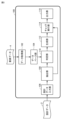
- FIG. 2 is a block diagram showing an example of the functional configuration of the design support apparatus according to the first embodiment.
- the design support apparatus 100 includes a data acquisition section 102, a database section 104, a design data input section 106, an extraction section 108, a determination section 110, a generation section 112, and a check execution section 114. and an output section 116.
- the database unit 104 is realized by the main storage device 152 or the secondary storage device 154.
- each function other than the database unit 104 is realized by the processor 150 executing a program, but may also be realized by a dedicated hardware circuit.
- the data acquisition unit 102 acquires element data 4 regarding each component constituting the electronic circuit board (for example, accepts input of element data 4).
- Element data 4 includes IC-related information regarding the IC included in the electronic circuit board, pattern-related information regarding the wiring pattern on the electronic circuit board, and specification information of the electronic circuit board (for example, product application of the electronic circuit board, amount of current, etc.). (including) and (including).
- the IC related information includes package characteristic information regarding the characteristics of the IC package and package type information indicating the type of the IC package.
- the package characteristic information includes the outline shape of the IC package (for example, the number of sides of the outline), the terminal shape of the IC package (for example, rectangular, circular, etc.), and terminal position information (for example, the relationship between the package outline and the terminals). (information indicating positional relationships), etc.
- the package type information includes, for example, the name of the IC package such as BGA (Ball Grid Array), QFN (Quad Flat Non-leaded package), SOP (Small Outline Package), and QFP (Quad Flat Package).
- the pattern related information includes pattern feature information indicating the characteristics of the wiring pattern and pattern type information indicating the type of the wiring pattern.
- the pattern characteristic information includes the material of the wiring pattern, the dielectric constant of the circuit board on which the wiring pattern is provided, the layer structure of the circuit board, the impedance value of the wiring pattern, the wiring pattern shape (for example, length, width, shape), IC This includes the ratio of the maximum width of the wiring pattern connected to the terminal to the dimension of the terminal of the package.
- the pattern type information includes, for example, name (or usage) information of wiring patterns such as Signal (signal pattern), VCC (power supply pattern), and GND.
- the database unit 104 stores various element data 4 input to the data acquisition unit 102. Specifically, the database unit 104 stores characteristic information including the shape of the components constituting the electronic circuit board (for example, package characteristic information and pattern characteristic information), and type information of the components (for example, package type information and pattern characteristic information). (type information) is stored.
- characteristic information including the shape of the components constituting the electronic circuit board (for example, package characteristic information and pattern characteristic information), and type information of the components (for example, package type information and pattern characteristic information). (type information) is stored.
- the database unit 104 stores, as reference information, a table R1 that associates package characteristic information (for example, the external linear shape of the IC package, the terminal shape of the IC package, and the terminal position information) with package type information.
- Table R1 is data referenced by determination unit 110, which will be described later.
- the database unit 104 stores a table R2 that associates pattern feature information with pattern type information.
- table R2 includes the ratio of the maximum width of the wiring pattern to the terminal dimensions of the IC package in the signal pattern, and a list and numerical distribution of impedance values of the wiring pattern.
- table R2 includes the ratio in the power supply pattern, a list of the impedance values, and a numerical distribution.
- the design data input unit 106 receives input of design data 2 of the target electronic circuit board to be subjected to the design rule check.
- the design data 2 is CAD data of the target electronic circuit board.
- the extraction unit 108 extracts feature information including the shapes of the components constituting the target electronic circuit board by analyzing the design data 2. First, the extraction unit 108 determines whether or not the design data 2 includes type information (for example, package type information, pattern type information) of the components constituting the target electronic circuit board. Package type information and pattern type information are information necessary to execute design rule checks according to these types. In other words, the extraction unit 108 determines whether or not the design data 2 lacks information for appropriately executing the design rule check.
- type information for example, package type information, pattern type information
- the package information input field for the IC library of design data 2 is blank, or the specified package name (e.g., BGA, QFN) is not entered in the package information input field (e.g., just a list of numbers, etc.) In this case, the extraction unit 108 determines that the design data 2 does not include package type information. On the other hand, if a prescribed package name is entered in the package information input field, the extraction unit 108 determines that the design data 2 includes package type information.
- the specified package name e.g., BGA, QFN
- the extraction unit 108 determines that the design data 2 does not include pattern type information. On the other hand, if a prescribed pattern name is entered in the net attribute input field, the extraction unit 108 determines that the design data 2 includes pattern type information.
- the extraction unit 108 determines that the design data 2 does not include type information of a component constituting the target electronic circuit board using the above method, it extracts characteristic information of the component.
- the extraction unit 108 extracts, as package characteristic information, the outline shape of the IC package, the terminal shape of the IC package, and information indicating the positional relationship between the IC package outline and the terminals of the IC package (i.e., terminal positions). information).
- the extraction unit 108 extracts, as pattern feature information, the maximum width of a wiring pattern connected to a terminal of an IC package (that is, the maximum pattern width) with respect to the terminal dimensions of an IC package included in the target electronic circuit board. , and the impedance value of the wiring pattern. Note that the details of the feature information extraction method by the extraction unit 108 will be described later.
- the determination unit 110 determines the target electronic circuit corresponding to the extracted feature information. Determine type information of the constituent elements constituting the board. Specifically, the determining unit 110 determines the package type information (eg, BGA, QFN) corresponding to the extracted package characteristic information by comparing the extracted package characteristic information with table R1. Further, the determining unit 110 determines pattern type information (for example, signal pattern, power pattern) corresponding to the extracted pattern characteristic information by comparing the extracted pattern characteristic information with table R2.
- the package type information eg, BGA, QFN
- the determining unit 110 determines pattern type information (for example, signal pattern, power pattern) corresponding to the extracted pattern characteristic information by comparing the extracted pattern characteristic information with table R2.
- the generation unit 112 generates new design data by adding the type information determined by the determination unit 110 to the design data 2.
- the check execution unit 114 executes a design rule check on the new design data generated by the generation unit 112. Specifically, the check execution unit 114 executes a design rule check on the new design data according to the added package type information and pattern type information.
- the extraction unit 108 determines that the design data 2 includes type information of the components constituting the target electronic circuit board
- the design data acquired by the design data input unit 106 is 2 is input to the check execution unit 114.
- the check execution unit 114 executes a design rule check on the design data 2 acquired by the design data input unit 106.
- the output unit 116 outputs the design rule check results by the check execution unit 114. For example, the output unit 116 displays the design rule check results on the display 160, or transmits the design rule check results to an external device.
- FIG. 3 is a diagram showing an example of a symbol graphic of an IC package.
- extracting unit 108 extracts a rectangular shape with the largest diagonal length among the graphic groups forming the symbol graphic of IC package 11 as outline line 12 of IC package 11 (i.e., (extract the package outline).
- the extraction unit 108 extracts a plurality of figures other than the outline line 12 from the group of figures constituting the symbol figure of the IC package 11 as the terminals 13 of the IC package 11 (that is, extracts the terminal shape of the IC package).
- the extraction unit 108 extracts information indicating the positional relationship between the outline 12 of the IC package and the terminals 13 (ie, terminal position information).
- the terminal position information includes information indicating whether the terminal 13 exists inside the closed region formed by the outline line 12 or outside the closed region.
- Package type information is determined based on these extracted information.
- FIG. 4 is a diagram showing an example of an information table of an IC package.
- column 51 shows the part number
- column 52 shows the terminal shape
- column 53 shows the position of the terminal with respect to the outline (hereinafter also simply referred to as "terminal position").
- Column 54 shows the number of sides of the IC package outline on which the terminal exists (hereinafter also simply referred to as "number of sides”)
- column 55 shows the IC package name.
- the information table 14 is composed of these five items.
- the terminal position "inside the closed area” indicates that the terminal exists inside the closed area formed by the outline, and the terminal position "outside the closed area” indicates that the terminal exists outside the closed area. ing.
- the terminal shape in column 52, the position of the terminal in column 53, and the number of sides in column 54 correspond to the characteristic information of the IC package extracted by the extraction unit 108.
- the IC package name in column 55 corresponds to package type information determined by determination unit 110 based on the characteristic information of the IC package. Note that the part number in the column 51 is extracted from the design data 2 (for example, by reading character information written on the CAD data).
- FIG. 5 is an updated diagram of the IC package information table in FIG. 4.
- the information table 14 in FIG. 5 is an updated version of the column 55 of the information table 14 in FIG. Specifically, in the information table 14 of FIG. 4, the column 55 is blank, but in the information table 14 of FIG. 5, it is understood that the IC package name is written in the column 55.
- the determining unit 110 determines the IC package name in the column 55 using a table R1 that associates package characteristic information (for example, the external linear shape of the IC package, the terminal shape of the IC package, and the terminal position information) with the package type information. judge. Specifically, the determining unit 110 determines the IC package name in the column 55 by comparing the information in columns 52, 53, and 54 of the information table 14 with table R1 stored in the database unit 104. In table R1, the same feature information as the feature information in columns 52, 53, and 54 is searched, and the package type information associated with the feature information found is the package type corresponding to the feature information in columns 52, 53, and 54. Extracted as information.
- package characteristic information for example, the external linear shape of the IC package, the terminal shape of the IC package, and the terminal position information
- the IC package name corresponding to the "circular” terminal shape is "BGA”.
- the IC package name corresponding to the terminal shape “rectangular”, the terminal position "inside a closed area”, and the number of sides "4" is “QFN”.
- the IC package name corresponding to the terminal shape “rectangular”, the terminal position "outside the closed area”, and the number of sides "4" is "QFP”.
- the IC package name corresponding to the terminal shape "rectangular”, the terminal position "outside the closed area", and the number of sides "2" is "SOP".
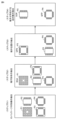
- FIG. 6 is a diagram for explaining the flow until the IC package name is specified. Referring to FIG. 6, in step S1, for each of the IC packages P1 to P4, a rectangular shape with the largest diagonal length is extracted as the outline of the IC package, as described in FIG.
- step S2 the terminal shapes of IC packages P1 to P4 are extracted.
- the terminal shape of IC package P1 is "circular", and the terminal shape of IC packages P2 to P4 is "rectangular”. Therefore, the type of IC package P1 is specified as "BGA”.
- step S3 the terminal positions of IC packages P2 to P4 are extracted.
- the terminal position of IC package P3 is "within the closed area", and the terminal position of IC packages P2 and P4 is "outside the closed area”. Therefore, the type of IC package P3 is specified as "QFN".
- step S4 the number of sides of the package outline where the terminals of IC packages P2 and P4 are present is extracted.
- the "number of sides” in IC package P2 is “2”
- the “number of sides” in IC package P4 is "4". Therefore, the type of IC package P2 is specified as “SOP”, and the type of IC package P4 is specified as "QFP".
- ⁇ Pattern type determination method> The design constraints of the signal pattern and the design constraints of the power supply pattern included in the design data are different. Therefore, when performing a design rule check on design data, it is necessary to specify the type of wiring pattern included in the design data in advance.
- FIG. 7 is a diagram showing an example of a wiring pattern connected to a terminal of an IC package. Referring to FIG. 7, power supply pattern 19 and signal pattern 21 connected to terminal 17 of IC package 16 are shown.
- the rate of change in pattern width is significantly different between the power supply pattern 19 and the signal pattern 21 near the terminal 17 of the IC package 16. Specifically, when comparing the terminal dimension 18 and the maximum pattern width 20 of the power supply pattern 19, the maximum pattern width 20 of the power supply pattern 19 is larger than the terminal dimension 18. On the other hand, the maximum pattern width 22 of the signal pattern 21 is not much different from the terminal dimension 18 due to impedance matching of the signal pattern wiring. That is, the signal pattern 21 has a smaller ratio of the maximum width of the wiring pattern connected to the terminal of the IC package to the terminal dimension of the IC package than the power supply pattern 19.
- the impedance value of the power supply pattern 19 is considerably smaller than the impedance value of the signal pattern 21 in order to suppress the influence of power supply noise. That is, the impedance value of the signal pattern 21 is much larger than the impedance value of the power supply pattern 19.
- power supply patterns and signal patterns can be classified based on the ratio of the maximum pattern width to the terminal dimensions of the IC package and the impedance value of the wiring pattern.
- the impedance value of the wiring pattern is calculated by a known method based on the positional relationship between the wiring pattern shape and GND, and the layer structure of the circuit board.
- FIG. 8 is a diagram showing an example of a wiring pattern information table.
- column 61 indicates pattern numbers.
- Column 62 shows the ratio of the maximum pattern width to the terminal dimensions of the IC package included in the electronic circuit board.
- Column 63 shows the impedance value of the wiring pattern, and column 64 shows the pattern name.
- the ratio in column 62 and the impedance value in column 63 correspond to the characteristic information of the wiring pattern extracted by the extraction unit 108.
- the pattern names in the column 64 correspond to pattern type information determined by the determination unit 110 based on the characteristic information of the wiring pattern. Note that the pattern number in the column 61 is extracted from the design data 2 (for example, by reading character information written on the CAD data).
- FIG. 9 is an updated diagram of the wiring pattern information table in FIG. 8.
- the information table 24 in FIG. 9 is an updated version of the column 64 of the information table 24 in FIG. Specifically, in the information table 24 of FIG. 8, the column 64 was blank, but in the information table 24 of FIG. 9, it is understood that the pattern name is written in the column 64.
- the determining unit 110 determines the pattern name in the column 64 using a table R2 that associates pattern characteristic information (for example, the ratio of the maximum width pattern to the terminal dimension of the IC package, the impedance value of the wiring pattern) and the pattern type information. judge. Specifically, the determination unit 110 determines the pattern name in column 64 by comparing the information in columns 62 and 63 of information table 24 with table R2. Table R2 is searched for the same feature information as the feature information in columns 62 and 63, and pattern type information associated with the feature information is extracted as pattern type information corresponding to the feature information in columns 62 and 63.
- pattern characteristic information for example, the ratio of the maximum width pattern to the terminal dimension of the IC package, the impedance value of the wiring pattern
- the pattern name corresponding to the ratio X1 of the maximum pattern width to the terminal dimension and the impedance value Z1 is "VCC”
- the pattern name corresponding to the ratio X2 and the impedance value Z2 is "Signal”.
- IC package name information indicating the type of IC package constituting the electronic circuit board
- type of wiring pattern are included in the design data of the electronic circuit board input to the design support device. Even if the information (for example, pattern name) is not included, the IC package name and pattern name can be determined by analyzing the design data. Therefore, an appropriate design rule check can be performed based on the design constraints depending on the type of IC package and the type of wiring pattern. Furthermore, by displaying the execution results of appropriate design rule checks on a display or the like, it is also possible to reduce the design load on the designer.
- Embodiment 2 a configuration for estimating an IC package name and a pattern name using machine learning will be described.
- the hardware configuration of the design support apparatus according to the second embodiment is similar to that of the first embodiment.
- FIG. 10 is a block diagram showing an example of the functional configuration of the design support apparatus according to the second embodiment.
- the design support apparatus 100A includes a design data input section 106, an extraction section 108A, a generation section 112, a check execution section 114, an output section 116, a learning section 250, and a learned model storage. section 256 and estimation section 260.
- the learned model storage unit 256 is realized by the main storage device 152 or the secondary storage device 154.
- each function other than the trained model storage section 256 is realized by the processor 150 executing a program, but may also be realized by a dedicated hardware circuit.
- the learning section 250 includes a data acquisition section 252 and a model generation section 254.
- the data acquisition unit 252 acquires the learning data 6 (receives input).
- the learning data 6 includes learning data L1 and L2.
- the learning data L1 includes package characteristic information including the shape of the components constituting the electronic circuit board (for example, the external linear shape of the IC package, the terminal shape of the IC package, and terminal position information), and the electronic Specification information of the circuit board (for example, product specifications such as the product use of the electronic circuit board and the amount of current) is included.
- the learning data L1 is a data set in which package feature information and specification information are associated with each other.
- the learning data L2 includes pattern characteristic information including the shape of the wiring pattern constituting the electronic circuit board (for example, the material of the wiring pattern, the dielectric constant of the circuit board, the layer structure of the circuit board, the impedance value of the wiring pattern, the wiring pattern shape, ratio of maximum pattern width to terminal dimensions), and specification information of the electronic circuit board.
- the learning data L2 is a data set in which package feature information and specification information are associated with each other.
- the model generation unit 254 uses the learning data L1 to generate a learned model M1 for estimating package type information of an IC package constituting an electronic circuit board from the package characteristic information and specification information. Furthermore, the model generation unit 254 uses the learning data L2 to generate a learned model M2 for estimating pattern type information of a wiring pattern forming an electronic circuit board from the pattern feature information and specification information.
- the learning algorithm used by the model generation unit 254 can be a known algorithm such as supervised learning, unsupervised learning, or reinforcement learning.
- supervised learning a case will be described in which the K-means method (clustering), which is unsupervised learning, is applied.
- Unsupervised learning refers to a method in which learning data that does not include results (labels) is given to the learning section to learn features in the learning data.
- the model generation unit 254 learns the package type information by so-called unsupervised learning, for example, according to a grouping method using the K-means method.
- the K-means method is a non-hierarchical clustering algorithm, which uses the average of clusters to classify a given number of clusters into k.
- the K-means method is processed as follows. First, clusters are randomly assigned to each data xi. Next, the center Vj of each cluster is calculated based on the allocated data. The distance between each xi and each Vj is then determined and xi is reassigned to the nearest central cluster. Then, if the cluster assignments of all xi do not change in the above process, or if the amount of change falls below a certain threshold set in advance, it is determined that convergence has been achieved and the process ends.
- the model generation unit 254 performs so-called unsupervised learning according to the learning data L1 created based on the combination of package characteristic information and electronic circuit board specification information acquired by the data acquisition unit 252.
- the package type information (for example, IC package name) is learned, and a learned model M1 is generated.
- the learned model M1 classifies the learning data L1 into a plurality of groups according to the following criteria.
- the trained model M1 classifies group G1 corresponding to the terminal shape “circular” as “BGA”, and classifies group G2 corresponding to the terminal shape “rectangular” and the terminal position "inside closed area” as “QFN”. do.
- the trained model M1 classifies the group G3 corresponding to the terminal shape “rectangular”, the terminal position "outside the closed area”, and the number of sides of the IC package outline where the terminal is "2" into “SON”, and classifies the terminal into "SON”.
- the group G4 corresponding to the shape "rectangle”, the terminal position "outside the closed area", and the number of sides "4" is classified as "QFP".
- the model generation unit 254 generates pattern type information (for example, a pattern name) is learned, and a learned model M2 is generated.
- pattern type information For example, a pattern name
- the trained model M2 classifies the group H1 corresponding to "the ratio of the maximum pattern width to the terminal dimension is less than the threshold Th" and "the impedance value is greater than or equal to the threshold Tz" as a "signal pattern”; Group H2 corresponding to "the impedance value is equal to or greater than the threshold value Th" and "the impedance value is less than the threshold value Tz" is classified as "power supply pattern”.
- the model generation unit 254 By performing the above learning, the model generation unit 254 generates learned models M1 and M2 for estimating package type information and pattern type information from the learning data L1 and L2, and , M2 are output to the trained model storage section 256.
- the learned model storage unit 256 stores learned models M1 and M2.
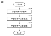
- FIG. 11 is a flowchart showing an example of the learning process of the design support device 100A. The steps in FIG. 11 are typically executed by the processor 150 (learning unit 250) of the design support apparatus 100A.
- the design support apparatus 100A obtains learning data L1 including package feature information and specification information, and learning data L2 including pattern feature information and specification information (step S10).
- learning data L1 and L2 including pattern feature information and specification information
- the design support device 100A separately acquires package feature information, pattern feature information, and specification information, associates the package feature information and specification information to generate learning data L1, and associates the pattern feature information and specification information for learning. data L2 may be generated.
- the design support device 100A generates a learned model M1 by learning package type information through unsupervised learning according to the acquired learning data L1, and generates a pattern type M1 through unsupervised learning according to the acquired learning data L2.
- a trained model M2 is generated by learning the information (step S12).
- the design support device 100A stores the generated learned models M1 and M2 in the internal memory (for example, the secondary storage device 154) (step S14).
- the design data input unit 106 acquires design data 2 of the target electronic circuit board to be subjected to the design rule check.
- the extraction unit 108A determines whether the design data 2 includes type information of the components constituting the target electronic circuit board. If the type information is not included in the design data 2, the extraction unit 108A extracts characteristic information of the component (for example, package characteristic information and pattern characteristic information) and specification information of the target electronic circuit board.
- the estimation unit 260 estimates package type information (for example, IC package name) using the learned model M1 stored in the learned model storage unit 256. Specifically, the estimation unit 260 estimates the package type information by inputting the package feature information and specification information extracted by the extraction unit 108A to the learned model M1.
- package type information for example, IC package name
- the estimation unit 260 estimates pattern type information (for example, pattern name) using the learned model M2 stored in the learned model storage unit 256. Specifically, the estimation unit 260 estimates pattern type information by inputting the pattern feature information and specification information extracted by the extraction unit 108A to the learned model M2.
- pattern type information for example, pattern name
- the estimation unit 260 outputs the package type information and pattern type information estimated by the above method to the generation unit 112.
- the functions and processing of the generation unit 112, check execution unit 114, and output unit 116 are the same as those described in Embodiment 1, so detailed description thereof will not be repeated.
- the design data input is performed.
- the design data 2 acquired by the unit 106 is input to the check execution unit 114.
- the check execution unit 114 executes a design rule check on the design data 2 acquired by the design data input unit 106.
- package type information and pattern type information are output using learned models M1 and M2 learned by the model generation unit 254, but learned models M1 and M2 are acquired from other devices.
- it may be configured to output package type information and pattern type information using the learned models M1 and M2.
- FIG. 12 is a flowchart showing an example of the processing procedure of the design support device 100A. The steps in FIG. 12 are typically executed by the processor 150 of the design support apparatus 100A.
- the design support apparatus 100A acquires (extracts) package feature information, pattern feature information, and specification information from the design data 2 (step S20).
- the design support device 100A estimates package type information by inputting package feature information and specification information into the learned model M1, and estimates pattern type information by inputting pattern feature information and specification information into the learned model M2. (Step S22).
- the design support device 100A outputs the estimated package type information and pattern type information (step S24).
- the design support device 100A generates new design data by adding package type information and pattern type information to the design data 2 (step S26).
- the design support device 100A executes a design rule check on the new design data (step S28).
- the design support device 100A outputs the design rule check result (step S30).
- the second embodiment has the same advantages as the first embodiment.
- the design support apparatus 100 does not include type information (for example, package type information and pattern type information) of the components constituting the target electronic circuit board in the design data 2.
- type information for example, package type information and pattern type information
- the configuration is not limited to this configuration.
- the design support device 100 may automatically determine the relevant type information without determining whether or not the design data 2 includes the relevant type information. It may be configured to extract feature information of the constituent elements.
- Embodiment 2 a case has been described in which unsupervised learning is applied to the learning algorithm used by the estimation unit 260, but the present invention is not limited to this.
- the learning algorithm in addition to unsupervised learning, reinforcement learning, supervised learning, semi-supervised learning, etc. can also be applied.
- the learning algorithm used in the model generation unit 254 deep learning, which learns the extraction of the feature values themselves, can be used, and other known methods such as neural networks, genetic programming, functional Machine learning may be performed according to logic programming, support vector machines, etc.
- the method is not limited to non-hierarchical clustering using the K-means method as described above, but any other known method capable of clustering may be used.
- hierarchical clustering such as the shortest distance method may be used.
- the learning unit 250 and the estimating unit 260 are configured to be built into the design support apparatus 100A, but the configuration is not limited to this.
- the learning unit 250 and the estimation unit 260 may be connected to the design support device 100A via a network, for example, and may be separate devices from the design support device 100A. That is, a learning device including the learning section 250 and an estimating device including the estimating section 260 may be prepared separately from the design support device 100A. In this case, the learning device and the estimation device may exist on a cloud server.
- the external dimensions of the IC package are used to change the threshold values of design rule check items regarding the positional relationship between the IC package and peripheral circuit components (for example, bypass capacitors, resistors, inductors, etc.) It may be configured as follows.
- the package characteristic information regarding the characteristics of the IC package further includes external dimensions (for example, long side dimensions, short side dimensions, etc.) of the IC package.
- the extracting unit 108 or 108A extracts the IC package as package characteristic information in addition to the external linear shape of the IC package, the terminal shape of the IC package, and the terminal position information. Further extract the external dimensions of.
- the case of the extraction unit 108 will be explained as a representative example.
- FIG. 13 is a diagram showing an example of an information table of an IC package according to another embodiment.
- information table 14A is the information table 14 of FIG. 4 with column 56 added.
- Column 56 shows the short side dimensions of the IC package. This short side dimension is extracted by the extraction unit 108 as characteristic information of the IC package.
- the short side dimensions of the IC packages with part numbers 1 to 6 are K1a to K6a, respectively.
- FIG. 14 is a diagram for explaining the positional relationship between the IC package and peripheral circuit components.
- IC package 300 is an IC package (eg, BGA) in which terminals are arranged in a grid.
- the IC package 300 is provided with a plurality of power terminals (power pins) 303 and 304, for example. Further, the short side dimension of the IC package 300 is "K1a", and the long side dimension is "K1b".
- the power supply terminal of the IC package 300 and peripheral circuit components are wired.
- the power terminal 303 and the peripheral circuit component 31 are connected through the wiring pattern 45
- the power terminal 304 and the peripheral circuit component 32 are connected through the wiring pattern 46.
- the peripheral circuit components 31 and 32 are filter circuits such as bypass capacitors.
- the filter circuit is preferably placed in close proximity to the power supply terminal from the viewpoint of noise countermeasures.
- the back side of the IC package may not be usable due to restrictions on wiring.
- the filter circuit will be placed on the same surface (same layer) as the IC package.
- the shortest path length between the power supply terminal and the filter circuit depends on the external dimensions of the IC package. do.
- the terminals with the maximum shortest path length to the filter circuit are the terminals located in the center of the IC package (for example, the power supply terminals 303 and 304). Therefore, the shortest path length between the filter circuit placed near the outline of the IC package and the terminal located at the center of the IC package is approximately 1/2 of the short side dimension of the IC package.
- the short side dimension of the IC package is used to appropriately set the threshold value TH1 of the check items (for example, the check items regarding the positional relationship between peripheral circuit components and the IC package) in the design rule check executed by the check execution unit 114.
- the threshold value TH1 is set to, for example, 1/2 of the short side dimension K1a of the IC package 300. If the shortest path length between the terminal of the IC package 300 and the peripheral circuit component is less than the threshold TH1, the check execution unit 114 determines that the criterion is satisfied (that is, the distance between the power supply terminal and the peripheral circuit component is short and appropriate). ). On the other hand, if the shortest path length is equal to or greater than the threshold TH1, the check execution unit 114 determines that the criterion is not satisfied (that is, the distance between the power terminal and the peripheral circuit component is long and inappropriate).
- the shortest path length between the peripheral circuit component 31 and the power supply terminal 303 is "D1". Since the shortest path length D1 is less than the threshold value TH1, the check execution unit 114 determines that the positional relationship between the peripheral circuit component 31 and the power supply terminal 303 is appropriate. The shortest path length between the peripheral circuit component 32 and the power supply terminal 304 is "D2". Since the shortest path length D2 is greater than or equal to the threshold value TH1, the check execution unit 114 determines that the positional relationship between the peripheral circuit component 32 and the power supply terminal 304 is inappropriate, and outputs an error.
- the design data input unit 106 receives input of design data 2 of the target electronic circuit board.
- the extraction unit 108 extracts feature information including the shapes of the components constituting the target electronic circuit board by analyzing the design data 2.
- the information table 14A shown in FIG. 13 is created by the extraction unit 108 extracting the package characteristic information of the IC package. If package type information is not included in the design data 2, an information table 14A is created in which the IC package name is entered in column 55 of the information table 14A in FIG. be done. That is, as shown in FIG. 5, column 55 of the information table 14A is updated. For example, "BGA" is input as the IC package name corresponding to part number 1.
- the information table 14A is created in which the IC package name is entered in the column 55 based on the package type information extracted by the extraction unit 108.
- the extraction unit 108 also extracts information regarding the shape (eg, outline shape, external dimensions, etc.) and type of peripheral circuit components.
- the check execution unit 114 calculates a threshold TH1 for checking the positional relationship between the IC package and peripheral circuit components based on the external dimensions. Specifically, the check execution unit 114 refers to the updated information table 14A and calculates the threshold TH1 based on the short side dimension for an IC package in which terminals are arranged in a grid. For example, since the IC package corresponding to part number 1 is "BGA", the threshold TH1 for checking the positional relationship between the IC package and peripheral circuit components is calculated as "K1a ⁇ 1/2".
- the check execution unit 114 changes the default threshold to the threshold TH1, and uses the threshold TH1 to execute a design rule check regarding the positional relationship between the IC package and peripheral circuit components.
- the threshold value used in the design rule check is automatically changed to an appropriate value, so it is possible to assist the user's setting work.
- the user can also change the formula for calculating the threshold value TH1 or the value of the threshold value TH1 before executing the design rule check.
- FIG. 15 is a diagram for explaining a method of applying a threshold value when checking a design rule.
- an electronic circuit board 320 is mounted with an IC package 300 (eg, BGA) having terminals arranged in a grid pattern and peripheral circuit components 31A to 31E.
- IC package 300 eg, BGA
- peripheral circuit components 31A to 31E it is assumed that the terminals of IC package 300 and peripheral circuit components 31A to 31E are connected via wiring patterns.
- the check execution unit 114 performs graphic arithmetic processing to determine which of the peripheral circuit components 31A to 31E are located completely within the internal area 310 of the external contour, and which are located on the external contour of the IC package 300 or which are completely located within the internal area 310 of the external contour. Determine which peripheral circuit components are located entirely in the external area.
- the peripheral circuit components 31A and 31B are determined to be completely located in the internal region 310.
- the peripheral circuit component 31C is located on the outline line, and the peripheral circuit components 31D and 31E are located completely in the area outside the outline line.
- the check execution unit 114 applies the threshold TH1 as a threshold for checking the positional relationship between the peripheral circuit components 31C to 31E and the IC package 300. Specifically, the check execution unit 114 determines whether the shortest path length between each of the peripheral circuit components 31C to 31E and a terminal (for example, a power supply terminal) of the IC package 300 is less than a threshold value TH1. Note that the shortest path length between peripheral circuit components (for example, peripheral circuit components 31C and 31D) placed on a layer different from the surface (layer) on which the IC package 300 is mounted and the terminal of the IC package 300 is This is the total distance when connecting the VIA and the wiring pattern.
- a threshold value TH1 for checking the positional relationship between the peripheral circuit components 31C to 31E and the IC package 300. Specifically, the check execution unit 114 determines whether the shortest path length between each of the peripheral circuit components 31C to 31E and a terminal (for example, a power supply terminal) of the IC package 300 is less than a
- a prescribed value different from the threshold TH1 is applied to the threshold for checking the positional relationship between the peripheral circuit components 31A and 31B located in the internal region 310 and the IC package 300.
- the threshold value TH2 is inappropriate as a threshold value for checking the above-mentioned positional relationship.
- the design rule check can be executed using the threshold value TH1 based on the short side dimension, so that pseudo errors caused by executing the design rule check using an inappropriate threshold value (for example, the threshold value TH2) can be avoided. It becomes possible to suppress this.
- the configuration exemplified as the embodiment described above is an example of the configuration of the present disclosure, and it is also possible to combine it with another known technology, or a part of it may be modified without departing from the gist of the present disclosure. It is also possible to omit or otherwise configure the configuration. Further, in the embodiment described above, the processes and configurations described in other embodiments may be appropriately adopted and implemented.
- Design data 4 Element data, 6 Learning data, 12 Outline, 13, 17 Terminals, 14, 14A, 24 Information table, 18 Terminal dimensions, 19 Power supply pattern, 20, 22 Maximum pattern width, 21 Signal pattern, 31 , 32 peripheral circuit components, 45, 46 wiring pattern, 100, 100A design support device, 102, 252 data acquisition unit, 104 database unit, 106 design data input unit, 108, 108A extraction unit, 110 determination unit, 112 generation unit, 114 Check execution unit, 116 Output unit, 150 Processor, 152 Main storage, 154 Secondary storage, 156 Communication interface, 158 Input device, 160 Display, 162 Internal bus, 250 Learning unit, 254 Model generation unit, 256 Learned Model storage unit, 260 estimation unit, 303, 304 power terminal, 320 electronic circuit board.
Landscapes
- Engineering & Computer Science (AREA)
- Physics & Mathematics (AREA)
- Theoretical Computer Science (AREA)
- Computer Hardware Design (AREA)
- Evolutionary Computation (AREA)
- General Physics & Mathematics (AREA)
- General Engineering & Computer Science (AREA)
- Geometry (AREA)
- Artificial Intelligence (AREA)
- Computer Vision & Pattern Recognition (AREA)
- Medical Informatics (AREA)
- Software Systems (AREA)
- Manufacturing & Machinery (AREA)
- Microelectronics & Electronic Packaging (AREA)
- Design And Manufacture Of Integrated Circuits (AREA)
Abstract
設計支援装置(100)は、電子回路基板を構成する構成要素の形状を含む特徴情報と、構成要素の種類情報とを関連付けたリファレンス情報を記憶するデータベース部(104)と、デザインルールチェックの対象となる対象電子回路基板の設計データの入力を受け付けるデータ入力部(106)と、対象電子回路基板を構成する構成要素の形状を含む特徴情報を抽出する抽出部(108)と、抽出された特徴情報とリファレンス情報とに基づいて、抽出された特徴情報に対応する、対象電子回路基板を構成する構成要素の種類情報を判定する判定部(110)と、判定部(110)により判定された種類情報を設計データに追加した新たな設計データを生成する生成部(112)と、新たな設計データに対してデザインルールチェックを実行するチェック実行部(114)とを備える。
Description
本開示は、設計支援装置、および学習装置に関する。
近年、電子機器の高機能化に伴って、電子機器に搭載される回路基板が高密度化し、回路基板に実装される集積回路(IC:Integrated Circuit)の数およびその種類が増加している。これにより、設計負荷が大きくなっており、基板設計チェック等の基板設計の効率化が要求されている。基板設計の効率化として、回路基板の設計に用いられるCAD(Computer Aided Design)装置等に設けられる基板デザインルールチェック機能が知られている。このデザインルールチェック機能によって、設計された回路基板がEMC性能等のデザインルールを満たしているか否かがチェックされる。
国際公開第2020/079810号(特許文献1)は設計支援装置を開示している。設計支援装置は、幾何学的な計算によって設計データに対してデザインルールチェックを行ない、エラーであると判定された部分がセンタリングされた画像データを設計データから生成し、人工知能によって画像データに対してデザインルールチェックを行ない、当該デザインルールチェックの結果を表示する。
電子回路基板は、様々な種類の構成要素(例えば、ICパッケージ、配線パターン等)で構成されているため、各構成要素の種類に応じた設計制約に基づいてデザインルールチェックを実行する必要がある。そのため、電子回路基板の設計データに各構成要素の種類を示す情報が含まれていない場合には、各構成要素に対して適切なデザインルールチェックを実行することができない。特許文献1では、上述した構成により、デザインルールチェックによって判定されたエラーが真のエラーであるかどうかを確認する作業を効率化することを検討しているが、上記課題に対する解決手段を何ら教示または示唆していない。
本開示のある局面における目的は、電子回路基板を構成する構成要素に対して適切なデザインルールチェックを実行することが可能な技術を提供することである。
ある実施の形態に従う設計支援装置は、電子回路基板を構成する構成要素の形状を含む特徴情報と、構成要素の種類情報とを関連付けたリファレンス情報を記憶するデータベース部と、デザインルールチェックの対象となる対象電子回路基板の設計データの入力を受け付けるデータ入力部と、設計データを解析することにより、対象電子回路基板を構成する構成要素の形状を含む特徴情報を抽出する抽出部と、抽出された特徴情報と、データベース部に記憶されたリファレンス情報とに基づいて、抽出された特徴情報に対応する、対象電子回路基板を構成する構成要素の種類情報を判定する判定部と、判定部により判定された種類情報を設計データに追加した新たな設計データを生成する生成部と、新たな設計データに対してデザインルールチェックを実行するチェック実行部とを備える。
他の実施の形態に従う学習装置は、電子回路基板を構成する構成要素の形状を含む特徴情報と、電子回路基板の仕様情報とを含む学習用データを取得するデータ取得部と、学習用データを用いて、特徴情報と仕様情報とから、電子回路基板を構成する構成要素の種類情報を推定するための学習済モデルを生成するモデル生成部とを備える。
さらに他の実施の形態に従う設計支援装置は、デザインルールチェックの対象となる対象電子回路基板の設計データの入力を受け付けるデータ入力部と、設計データを解析することにより、対象電子回路基板を構成する構成要素の形状情報を含む特徴情報と、対象電子回路基板の仕様情報とを抽出する抽出部と、特徴情報および仕様情報から構成要素の種類情報を推定するための学習済モデルに、抽出部により抽出された特徴情報および仕様情報を入力することにより種類情報を推定する推定部とを備える。
本開示によると、電子回路基板を構成する構成要素に応じたデザインルールチェックを実行することができる。
以下、図面を参照しつつ、本実施の形態について説明する。以下の説明では、同一の部品には同一の符号を付してある。それらの名称および機能も同じである。したがって、それらについての詳細な説明は繰り返さない。
実施の形態1.
本実施の形態に従う設計支援装置は、回路素子が配置された電子回路基板(例えば、プリント回路基板)の設計データ(例えば、CADデータ)に対してデザインルールチェックを実行する機能を有する。以下、設計支援装置100の構成、処理等について具体的に説明する。
本実施の形態に従う設計支援装置は、回路素子が配置された電子回路基板(例えば、プリント回路基板)の設計データ(例えば、CADデータ)に対してデザインルールチェックを実行する機能を有する。以下、設計支援装置100の構成、処理等について具体的に説明する。
<ハードウェア構成>
図1は、設計支援装置100のハードウェア構成の一例を示す図である。設計支援装置100は、マイクロコンピュータを主体に構成されている。具体的には、設計支援装置100は、プロセッサ150と、主記憶装置152と、二次記憶装置154と、通信インターフェイス156と、入力装置158と、ディスプレイ160とを含む。これらのコンポーネントは、内部バス162を介して互いに通信可能に接続されている。
図1は、設計支援装置100のハードウェア構成の一例を示す図である。設計支援装置100は、マイクロコンピュータを主体に構成されている。具体的には、設計支援装置100は、プロセッサ150と、主記憶装置152と、二次記憶装置154と、通信インターフェイス156と、入力装置158と、ディスプレイ160とを含む。これらのコンポーネントは、内部バス162を介して互いに通信可能に接続されている。
プロセッサ150は、典型的には、CPU(Central Processing Unit)あるいはMPU(Multi Processing Unit)といった演算処理部であり、二次記憶装置154にインストールされているOS(Operating System)を含む各種プログラムを読出して、主記憶装置152に展開しつつ実行する。
主記憶装置152は、典型的には、DRAM(Dynamic Random Access Memory)などの揮発性記憶媒体であり、プロセッサ150によって実行されるOSを含む各種プログラムのコードの他、各種プログラムの実行に必要な各種ワークデータを保持する。二次記憶装置154は、ハードディスクあるいはSSD(Solid State Drive)などの不揮発性記憶媒体であり、OSを含む各種プログラムの他、各種設定値などを保持する。
通信インターフェイス156は、プロセッサ150と外部装置との間のデータ伝送を仲介する。通信インターフェイス156を介した通信は、インターネット、ワイドエリアネットワーク(WAN)、ローカルエリアネットワーク(LAN)、イーサネット(登録商標)ネットワーク、有線ネットワークまたは無線ネットワーク等、あるいは、これらの組み合わせを用いて行なわれる。
入力装置158は、設計支援装置に対する操作入力を受け付ける。入力装置158は、例えば、キーボード、ボタン、マウス、タッチパネルなどによって実現される。
ディスプレイ160は、例えば、液晶ディスプレイ、有機EL(Electro Luminescence)ディスプレイ等である。ディスプレイ160は、設計支援装置100と一体的に構成されてもよいし、設計支援装置100とは別個に構成されてもよい。
なお、図1の例とは異なり、設計支援装置100の少なくとも一部をFPGA(Field Programmable Gate Array)および、ASIC(Application Specific Integrated Circuit)等の回路を用いて構成することも可能である。
<機能構成>
図2は、実施の形態1に従う設計支援装置の機能構成例を示すブロック図である。図2を参照して、設計支援装置100は、データ取得部102と、データベース部104と、設計データ入力部106と、抽出部108と、判定部110と、生成部112と、チェック実行部114と、出力部116とを含む。データベース部104は、主記憶装置152あるいは二次記憶装置154により実現される。典型的には、データベース部104以外の各機能は、プロセッサ150がプログラムを実行することにより実現されるが、専用のハードウェア回路により実現されてもよい。
図2は、実施の形態1に従う設計支援装置の機能構成例を示すブロック図である。図2を参照して、設計支援装置100は、データ取得部102と、データベース部104と、設計データ入力部106と、抽出部108と、判定部110と、生成部112と、チェック実行部114と、出力部116とを含む。データベース部104は、主記憶装置152あるいは二次記憶装置154により実現される。典型的には、データベース部104以外の各機能は、プロセッサ150がプログラムを実行することにより実現されるが、専用のハードウェア回路により実現されてもよい。
データ取得部102は、電子回路基板を構成する各構成要素に関する要素データ4を取得する(例えば、要素データ4の入力を受け付ける)。要素データ4は、電子回路基板に含まれるICに関するIC関連情報と、電子回路基板における配線パターンに関するパターン関連情報と、電子回路基板の仕様情報(例えば、電子回路基板の製品用途、電流量等を含む。)とを含む。
IC関連情報は、ICパッケージの特徴に関するパッケージ特徴情報と、ICパッケージの種類を示すパッケージ種類情報とを含む。パッケージ特徴情報は、ICパッケージの外形線形状(例えば、外形線の辺の数)、ICパッケージの端子形状(例えば、矩形、円形等)、および端子位置情報(例えば、パッケージ外形線と端子との位置関係を示す情報)等を含む。パッケージ種類情報は、例えば、BGA(Ball Grid Array)、QFN(Quad Flat Non-leaded package)、SOP(Small Outline Package)、QFP(Quad Flat Package)等のICパッケージの名称を含む。
パターン関連情報は、配線パターンの特徴を示すパターン特徴情報と、配線パターンの種類を示すパターン種類情報とを含む。パターン特徴情報は、配線パターンの材質、配線パターンが設けられる回路基板の比誘電率、当該回路基板の層構成、配線パターンのインピーダンス値、配線パターン形状(例えば、長さ、幅、図形)、ICパッケージの端子の寸法に対する当該端子に接続される配線パターンの最大幅の比率等を含む。パターン種類情報は、例えば、Signal(信号パターン)、VCC(電源パターン)、GND等の配線パターンの名称(または用途)情報を含む。
データベース部104は、データ取得部102に入力された各種の要素データ4を蓄積している。具体的には、データベース部104は、電子回路基板を構成する構成要素の形状を含む特徴情報(例えば、パッケージ特徴情報およびパターン特徴情報)と、構成要素の種類情報(例えば、パッケージ種類情報およびパターン種類情報)とを関連付けたリファレンス情報を記憶する。
データベース部104は、パッケージ特徴情報(例えば、ICパッケージの外形線形状、ICパッケージの端子形状、および端子位置情報)と、パッケージ種類情報とを関連付けたテーブルR1をリファレンス情報として記憶している。テーブルR1は、後述する判定部110において参照されるデータである。
データベース部104は、パターン特徴情報とパターン種類情報とを関連付けたテーブルR2を記憶している。例えば、テーブルR2は、信号パターンにおける、ICパッケージの端子寸法に対する配線パターンの最大幅の比率と、配線パターンのインピーダンス値の一覧ならびに数値分布とを含む。同様に、テーブルR2は、電源パターンにおける当該比率と、当該インピーダンス値の一覧ならびに数値分布とを含む。
設計データ入力部106は、デザインルールチェックの対象となる対象電子回路基板の設計データ2の入力を受け付ける。典型的には、設計データ2は、対象電子回路基板のCADデータである。
抽出部108は、設計データ2を解析することにより、対象電子回路基板を構成する構成要素の形状を含む特徴情報を抽出する。まず、抽出部108は、設計データ2の中に、対象電子回路基板を構成する構成要素の種類情報(例えば、パッケージ種類情報、パターン種類情報)が含まれているか否かを判断する。パッケージ種類情報およびパターン種類情報は、これらの種類に応じたデザインルールチェックを実行するために必要な情報である。換言すると、抽出部108は、設計データ2において、デザインルールチェックを適切に実行するための情報が不足しているか否かを判断する。
例えば、設計データ2のICライブラリのパッケージ情報入力欄が空欄である、あるいは、パッケージ情報入力欄に規定のパッケージ名称(例えば、BGA、QFN)が入力されていない(例えば、単なる数字の羅列等)場合、抽出部108は設計データ2の中にパッケージ種類情報が含まれていないと判断する。一方、パッケージ情報入力欄に規定のパッケージ名称が入力されている場合、抽出部108は設計データ2の中にパッケージ種類情報が含まれていると判断する。
また、設計データ2のネットデータのネット属性入力欄が空欄である、あるいは、ネット属性入力欄に規定のパターン名称(例えば、VCC、GND、Signal)が入力されていない(例えば、単なる数字の羅列等)場合、抽出部108は設計データ2の中にパターン種類情報が含まれていないと判断する。一方、ネット属性入力欄に規定のパターン名称が入力されている場合、抽出部108は設計データ2の中にパターン種類情報が含まれていると判断する。
抽出部108は、上記方式により設計データ2の中に、対象電子回路基板を構成する構成要素の種類情報が含まれていないと判断した場合、当該構成要素の特徴情報を抽出する。ある局面では、抽出部108は、パッケージ特徴情報として、ICパッケージの外形線形状と、ICパッケージの端子形状と、ICパッケージ外形線とICパッケージの端子との位置関係を示す情報(すなわち、端子位置情報)とを抽出する。他の局面では、抽出部108は、パターン特徴情報として、対象電子回路基板に含まれるICパッケージの端子寸法に対する、当該ICパッケージの端子に接続される配線パターンの最大幅(すなわち、最大パターン幅)の比率と、配線パターンのインピーダンス値とを抽出する。なお、抽出部108による特徴情報の抽出方式の詳細については後述する。
判定部110は、抽出部108により抽出された特徴情報と、データベース部104に記憶されたリファレンス情報(例えば、テーブルR1,R2)とに基づいて、抽出された特徴情報に対応する、対象電子回路基板を構成する構成要素の種類情報を判定する。具体的には、判定部110は、抽出されたパッケージ特徴情報と、テーブルR1とを比較することによって、当該パッケージ特徴情報に対応するパッケージ種類情報(例えば、BGA、QFN)を判定する。また、判定部110は、抽出されたパターン特徴情報と、テーブルR2とを比較することによって、当該パターン特徴情報に対応するパターン種類情報(例えば、信号パターン、電源パターン)を判定する。
生成部112は、判定部110により判定された種類情報を設計データ2に追加した新たな設計データを生成する。
チェック実行部114は、生成部112により生成された新たな設計データに対してデザインルールチェックを実行する。具体的には、チェック実行部114は、追加されたパッケージ種類情報およびパターン種類情報に応じたデザインルールチェックを新たな設計データに対して実行する。
なお、抽出部108によって、設計データ2の中に、対象電子回路基板を構成する構成要素の種類情報が含まれていると判断された場合には、設計データ入力部106により取得された設計データ2がチェック実行部114に入力される。この場合、抽出部108による特徴情報の抽出処理、判定部110による種類情報の判定処理、および生成部112による設計データ2への種類情報の追加処理は実行されない。したがって、チェック実行部114は、設計データ入力部106により取得された設計データ2に対してデザインルールチェックを実行する。
出力部116は、チェック実行部114によるデザインルールチェック結果を出力する。例えば、出力部116は、デザインルールチェック結果をディスプレイ160に表示する、あるいは、デザインルールチェック結果を外部装置に送信する。
<パッケージ種類の判定方式>
図3は、ICパッケージのシンボル図形例を示す図である。図3を参照して、抽出部108は、ICパッケージ11のシンボル図形を構成する図形群のうち、対角線の長さが最も大きい矩形形状を、ICパッケージ11の外形線12として抽出(すなわち、ICパッケージの外形線形状を抽出)する。抽出部108は、ICパッケージ11のシンボル図形を構成する図形群のうち、外形線12以外の複数の図形をICパッケージ11の端子13として抽出(すなわち、ICパッケージの端子形状を抽出)する。抽出部108は、ICパッケージの外形線12と端子13との位置関係を示す情報(すなわち、端子位置情報)を抽出する。端子位置情報は、端子13が外形線12で構成される閉領域の内側に存在するか、閉領域の外側に存在するかを示す情報を含む。これらの抽出された情報に基づいて、パッケージ種類情報が判定される。
図3は、ICパッケージのシンボル図形例を示す図である。図3を参照して、抽出部108は、ICパッケージ11のシンボル図形を構成する図形群のうち、対角線の長さが最も大きい矩形形状を、ICパッケージ11の外形線12として抽出(すなわち、ICパッケージの外形線形状を抽出)する。抽出部108は、ICパッケージ11のシンボル図形を構成する図形群のうち、外形線12以外の複数の図形をICパッケージ11の端子13として抽出(すなわち、ICパッケージの端子形状を抽出)する。抽出部108は、ICパッケージの外形線12と端子13との位置関係を示す情報(すなわち、端子位置情報)を抽出する。端子位置情報は、端子13が外形線12で構成される閉領域の内側に存在するか、閉領域の外側に存在するかを示す情報を含む。これらの抽出された情報に基づいて、パッケージ種類情報が判定される。
図4は、ICパッケージの情報テーブルの一例を示す図である。図4を参照して、情報テーブル14において、列51は部品番号を示し、列52は端子形状を示し、列53は外形線に対する端子の位置(以下、単に「端子位置」とも称する。)を示し、列54は端子が存在するICパッケージ外形線の辺の数(以下、単に「辺の数」とも称する。)を示し、列55はICパッケージ名称を示している。情報テーブル14はこれらの5つの項目で構成される。端子位置「閉領域内」は、端子が外形線で構成される閉領域の内側に存在することを示し、端子位置「閉領域外」は、端子が当該閉領域の外側に存在することを示している。
列52における端子形状、列53における端子の位置および列54における辺の数は、抽出部108により抽出されるICパッケージの特徴情報に相当する。列55におけるICパッケージ名称は、ICパッケージの特徴情報に基づいて判定部110により判定されるパッケージ種類情報に相当する。なお、列51における部品番号は設計データ2から抽出(例えば、CADデータ上に記載されている文字情報等を読み取ることによって抽出)される。
図5は、図4のICパッケージの情報テーブルを更新した図である。図5の情報テーブル14は、図4の情報テーブル14の列55を更新したものである。具体的には、図4の情報テーブル14では列55が空欄となっていたが、図5の情報テーブル14では、列55にICパッケージ名称が記載されていることが理解される。
判定部110は、パッケージ特徴情報(例えば、ICパッケージの外形線形状、ICパッケージの端子形状、および端子位置情報)とパッケージ種類情報とを関連付けたテーブルR1を用いて、列55におけるICパッケージ名称を判定する。具体的には、判定部110は、情報テーブル14の列52,53,54の情報と、データベース部104に記憶されたテーブルR1とを比較することにより、列55におけるICパッケージ名称を判定する。テーブルR1において、列52,53,54の特徴情報と同一の特徴情報を検索し、検索された特徴情報に関連付けられたパッケージ種類情報が、列52,53,54の特徴情報に対応するパッケージ種類情報として抽出される。
端子形状「円形」に対応するICパッケージ名称は「BGA」である。端子形状「矩形」、端子位置「閉領域内」および辺の数「4」に対応するICパッケージ名称は「QFN」である。端子形状「矩形」、端子位置「閉領域外」および辺の数「4」に対応するICパッケージ名称は「QFP」である。端子形状「矩形」、端子位置「閉領域外」および辺の数「2」に対応するICパッケージ名称は「SOP」である。
このように、上記の端子形状、端子位置および辺の数に基づいてICパッケージ名称が特定される理由について説明する。
図6は、ICパッケージ名称が特定されるまでの流れを説明するための図である。図6を参照して、ステップS1において、図3で説明したように、ICパッケージP1~P4の各々について、対角線の長さが最も大きい矩形形状が当該ICパッケージの外形線として抽出される。
ステップS2において、ICパッケージP1~P4の端子形状が抽出される。ICパッケージP1の端子形状は「円形」であり、ICパッケージP2~P4の端子形状は「矩形」である。そのため、ICパッケージP1の種類は「BGA」であると特定される。
ステップS3において、ICパッケージP2~P4の端子位置が抽出される。ICパッケージP3の端子位置は「閉領域内」であり、ICパッケージP2,P4の端子位置は「閉領域外」である。そのため、ICパッケージP3の種類は「QFN」であると特定される。
ステップS4において、ICパッケージP2,P4の端子が存在するパッケージ外形線の辺の数が抽出される。ICパッケージP2における「辺の数」は“2”であり、ICパッケージP4における「辺の数」は“4”である。そのため、ICパッケージP2の種類は「SOP」であると特定され、ICパッケージP4の種類は「QFP」であると特定される。
<パターン種類の判定方式>
設計データに含まれる信号パターンの設計制約と電源パターンの設計制約は異なる。そのため、設計データに対してデザインルールチェックを実行する場合には、設計データに含まれる配線パターンの種類を予め特定しておく必要がある。
設計データに含まれる信号パターンの設計制約と電源パターンの設計制約は異なる。そのため、設計データに対してデザインルールチェックを実行する場合には、設計データに含まれる配線パターンの種類を予め特定しておく必要がある。
図7は、ICパッケージの端子に接続された配線パターンの一例を示す図である。図7を参照して、ICパッケージ16の端子17に接続される電源パターン19および信号パターン21が示されている。
電源パターン19と信号パターン21とでは、ICパッケージ16の端子17付近において、パターン幅の変化率が大きく異なる。具体的には、端子寸法18と電源パターン19の最大パターン幅20とを比較すると、電源パターン19の最大パターン幅20の方が端子寸法18よりも大きい。一方、信号パターン21の最大パターン幅22は、信号パターン配線のインピーダンス整合のため、端子寸法18と大差がない。すなわち、信号パターン21は電源パターン19よりも、ICパッケージの端子寸法に対する、当該ICパッケージの端子に接続される配線パターンの最大幅の比率が小さい。
また、電源パターン19のインピーダンス値は、電源ノイズの影響を抑止するために、信号パターン21のインピーダンス値よりもかなり小さい。すなわち、信号パターン21のインピーダンス値は、電源パターン19のインピーダンス値よりも非常に大きい。
したがって、ICパッケージの端子寸法に対する最大パターン幅の比率と、配線パターンのインピーダンス値とに基づいて、電源パターンおよび信号パターンを分類することができる。なお、配線パターンのインピーダンス値は、配線パターン形状とGNDとの位置関係と、回路基板の層構成とに基づいて公知の方法により算出される。
図8は、配線パターンの情報テーブルの一例を示す図である。図8を参照して、情報テーブル24において、列61はパターン番号を示している。列62は、電子回路基板に含まれるICパッケージの端子寸法に対する最大パターン幅の比率を示している。列63は配線パターンのインピーダンス値を示し、列64はパターン名称を示している。
列62における比率および列63におけるインピーダンス値は、抽出部108により抽出される配線パターンの特徴情報に相当する。列64におけるパターン名称は、配線パターンの特徴情報に基づいて判定部110により判定されるパターン種類情報に相当する。なお、列61におけるパターン番号は、設計データ2から抽出(例えば、CADデータ上に記載されている文字情報等を読み取ることによって抽出)される。
図9は、図8の配線パターンの情報テーブルを更新した図である。図9の情報テーブル24は、図8の情報テーブル24の列64を更新したものである。具体的には、図8の情報テーブル24では列64が空欄となっていたが、図9の情報テーブル24では、列64にパターン名称が記載されていることが理解される。
判定部110は、パターン特徴情報(例えば、ICパッケージの端子寸法に対する最大幅パターンの比率、配線パターンのインピーダンス値)と、パターン種類情報とを関連付けたテーブルR2を用いて、列64におけるパターン名称を判定する。具体的には、判定部110は、情報テーブル24の列62,63の情報と、テーブルR2とを比較することにより、列64におけるパターン名称を判定する。テーブルR2において、列62,63の特徴情報と同一の特徴情報を検索し、当該特徴情報に関連付けられたパターン種類情報が、列62,63の特徴情報に対応するパターン種類情報として抽出される。
例えば、端子寸法に対する最大パターン幅の比率X1およびインピーダンス値Z1に対応するパターン名称は「VCC」であり、比率X2およびインピーダンス値Z2に対応するパターン名称は「Signal」である。
<利点>
実施の形態1によると、設計支援装置に入力される電子回路基板の設計データの中に、電子回路基板を構成するICパッケージの種類を示す情報(例えば、ICパッケージ名称)および配線パターンの種類を示す情報(例えば、パターン名称)が含まれていない場合であっても、設計データを解析することによりICパッケージ名称およびパターン名称を判定することができる。そのため、ICパッケージの種類および配線パターンの種類のそれぞれに応じた設計制約に基づいて、適切なデザインルールチェックを実行できる。また、適切なデザインルールチェックの実行結果をディスプレイ等に表示することにより、設計者の設計負荷を軽減することもできる。
実施の形態1によると、設計支援装置に入力される電子回路基板の設計データの中に、電子回路基板を構成するICパッケージの種類を示す情報(例えば、ICパッケージ名称)および配線パターンの種類を示す情報(例えば、パターン名称)が含まれていない場合であっても、設計データを解析することによりICパッケージ名称およびパターン名称を判定することができる。そのため、ICパッケージの種類および配線パターンの種類のそれぞれに応じた設計制約に基づいて、適切なデザインルールチェックを実行できる。また、適切なデザインルールチェックの実行結果をディスプレイ等に表示することにより、設計者の設計負荷を軽減することもできる。
実施の形態2.
実施の形態2では、機械学習を利用してICパッケージ名称およびパターン名称を推定する構成について説明する。実施の形態2に従う設計支援装置のハードウェア構成は、実施の形態1のそれと同様である。
実施の形態2では、機械学習を利用してICパッケージ名称およびパターン名称を推定する構成について説明する。実施の形態2に従う設計支援装置のハードウェア構成は、実施の形態1のそれと同様である。
<機能構成>
図10は、実施の形態2に従う設計支援装置の機能構成例を示すブロック図である。図10を参照して、設計支援装置100Aは、設計データ入力部106と、抽出部108Aと、生成部112と、チェック実行部114と、出力部116と、学習部250と、学習済モデル記憶部256と、推定部260とを含む。学習済モデル記憶部256は、主記憶装置152あるいは二次記憶装置154により実現される。典型的には、学習済モデル記憶部256以外の各機能は、プロセッサ150がプログラムを実行することにより実現されるが、専用のハードウェア回路により実現されてもよい。
図10は、実施の形態2に従う設計支援装置の機能構成例を示すブロック図である。図10を参照して、設計支援装置100Aは、設計データ入力部106と、抽出部108Aと、生成部112と、チェック実行部114と、出力部116と、学習部250と、学習済モデル記憶部256と、推定部260とを含む。学習済モデル記憶部256は、主記憶装置152あるいは二次記憶装置154により実現される。典型的には、学習済モデル記憶部256以外の各機能は、プロセッサ150がプログラムを実行することにより実現されるが、専用のハードウェア回路により実現されてもよい。
(学習フェーズ)
学習部250による機械学習によって生成された学習済モデルを学習済モデル記憶部256に記憶するための機能および処理について説明する。
学習部250による機械学習によって生成された学習済モデルを学習済モデル記憶部256に記憶するための機能および処理について説明する。
学習部250は、データ取得部252と、モデル生成部254とを含む。データ取得部252は、学習用データ6を取得する(入力を受け付ける)。学習用データ6は、学習用データL1,L2を含む。
具体的には、学習用データL1は、電子回路基板を構成する構成要素の形状を含むパッケージ特徴情報(例えば、ICパッケージの外形線形状、ICパッケージの端子形状、および端子位置情報)と、電子回路基板の仕様情報(例えば、電子回路基板の製品用途、電流量等の製品仕様)とを含む。学習用データL1は、パッケージ特徴情報および仕様情報を互いに関連付けたデータセットである。
学習用データL2は、電子回路基板を構成する配線パターンの形状を含むパターン特徴情報(例えば、配線パターンの材質、回路基板の比誘電率、回路基板の層構成、配線パターンのインピーダンス値、配線パターン形状、端子寸法に対する最大パターン幅の比率)と、電子回路基板の仕様情報とを含む。学習用データL2は、パッケージ特徴情報および仕様情報を互いに関連付けたデータセットである。
モデル生成部254は、学習用データL1を用いて、パッケージ特徴情報と仕様情報とから、電子回路基板を構成するICパッケージのパッケージ種類情報を推定するための学習済モデルM1を生成する。また、モデル生成部254は、学習用データL2を用いて、パターン特徴情報と仕様情報とから、電子回路基板を構成する配線パターンのパターン種類情報を推定するための学習済モデルM2を生成する。
モデル生成部254が用いる学習アルゴリズムは教師あり学習、教師なし学習、強化学習等の公知のアルゴリズムを用いることができる。本実施の形態では、一例として、教師なし学習であるK平均法(クラスタリング)を適用した場合について説明する。教師なし学習とは、結果(ラベル)を含まない学習用データを学習部に与えることで、それらの学習用データにある特徴を学習する手法をいう。
モデル生成部254は、例えば、K平均法によるグループ分け手法に従って、いわゆる教師なし学習により、パッケージ種類情報を学習する。
K平均法とは、非階層型クラスタリングのアルゴリズムであり、クラスタの平均を用い、与えられたクラスタ数をk個に分類する手法である。
具体的には、K平均法は以下のような流れで処理される。まず、各データxiに対してランダムにクラスタを割り振る。次いで、割り振ったデータをもとに各クラスタの中心Vjを計算する。次いで、各xiと各Vjとの距離を求め、xiを最も近い中心のクラスタに割り当て直す。そして、上記の処理で全てのxiのクラスタの割り当てが変化しなかった場合、あるいは変化量が事前に設定した一定の閾値を下回った場合に、収束したと判断して処理を終了する。
本実施の形態では、モデル生成部254は、データ取得部252によって取得されるパッケージ特徴情報、電子回路基板の仕様情報の組合せに基づいて作成される学習用データL1に従って、いわゆる教師なし学習により、パッケージ種類情報(例えば、ICパッケージ名称)を学習し、学習済モデルM1を生成する。学習済モデルM1は、次のような基準に従って、学習用データL1を複数のグループに分類する。
例えば、学習済モデルM1は、端子形状「円形」に対応するグループG1を「BGA」に分類し、端子形状「矩形」かつ端子位置「閉領域内」に対応するグループG2は「QFN」に分類する。学習済モデルM1は、端子形状「矩形」、端子位置「閉領域外」、かつ端子が存在するICパッケージ外形線の辺の数「2」に対応するグループG3を「SON」に分類し、端子形状「矩形」、端子位置「閉領域外」、かつ辺の数「4」に対応するグループG4を「QFP」に分類する。
また、モデル生成部254は、データ取得部252によって取得されるパターン特徴情報、電子回路基板の仕様情報の組合せに基づいて作成される学習用データL2に従って、いわゆる教師なし学習により、パターン種類情報(例えば、パターン名称)を学習し、学習済モデルM2を生成する。例えば、学習済モデルM2は、「端子寸法に対する最大パターン幅の比率が閾値Th未満」、かつ「インピーダンス値が閾値Tz以上」に対応するグループH1は「信号パターン」に分類し、「当該比率が閾値Th以上」、かつ「インピーダンス値が閾値Tz未満」に対応するグループH2は「電源パターン」に分類する。
モデル生成部254は、以上のような学習を実行することで、学習用データL1,L2からパッケージ種類情報およびパターン種類情報を推定するための学習済モデルM1,M2を生成し、学習済モデルM1,M2を学習済モデル記憶部256に出力する。学習済モデル記憶部256は、学習済モデルM1,M2を記憶する。
図11は、設計支援装置100Aの学習処理の一例を示すフローチャートである。図11のステップは、典型的には、設計支援装置100Aのプロセッサ150(学習部250)により実行される。
図11を参照して、設計支援装置100Aは、パッケージ特徴情報および仕様情報を含む学習用データL1と、パターン特徴情報および仕様情報を含む学習用データL2とを取得する(ステップS10)。なお、学習用データL1,L2が同時に取得する構成について説明するが、当該構成に限られない。設計支援装置100Aは、パッケージ特徴情報、パターン特徴情報および仕様情報を別々に取得して、パッケージ特徴情報および仕様情報を関連付けて学習用データL1を生成し、パターン特徴情報および仕様情報を関連付けて学習用データL2を生成してもよい。
設計支援装置100Aは、取得された学習用データL1に従って、教師なし学習によりパッケージ種類情報を学習することにより学習済モデルM1を生成し、取得された学習用データL2に従って、教師なし学習によりパターン種類情報を学習することにより学習済モデルM2を生成する(ステップS12)。
設計支援装置100Aは、内部メモリ(例えば、二次記憶装置154)に、生成された学習済モデルM1,M2を記憶する(ステップS14)。
(活用フェーズ)
学習部250による機械学習によって生成された学習済モデルを用いて、ICパッケージ名称およびパターン名称を推定するまでの流れについて説明する。
学習部250による機械学習によって生成された学習済モデルを用いて、ICパッケージ名称およびパターン名称を推定するまでの流れについて説明する。
図10を参照して、設計データ入力部106は、デザインルールチェックの対象となる対象電子回路基板の設計データ2を取得する。
抽出部108Aは、実施の形態1の抽出部108と同様に、設計データ2の中に対象電子回路基板を構成する構成要素の種類情報が含まれているか否かを判断する。抽出部108Aは、設計データ2の中に当該種類情報が含まれていない場合、当該構成要素の特徴情報(例えば、パッケージ特徴情報およびパターン特徴情報)および対象電子回路基板の仕様情報を抽出する。
推定部260は、学習済モデル記憶部256に記憶された学習済モデルM1を利用して、パッケージ種類情報(例えば、ICパッケージ名称)を推定する。具体的には、推定部260は、学習済モデルM1に対して、抽出部108Aにより抽出されたパッケージ特徴情報および仕様情報を入力することにより、パッケージ種類情報を推定する。
また、推定部260は、学習済モデル記憶部256に記憶された学習済モデルM2を利用して、パターン種類情報(例えば、パターン名称)を推定する。具体的には、推定部260は、学習済モデルM2に対して、抽出部108Aにより抽出されたパターン特徴情報および仕様情報を入力することにより、パターン種類情報を推定する。
推定部260は、上記方式により推定されたパッケージ種類情報およびパターン種類情報を生成部112に出力する。生成部112、チェック実行部114および出力部116の機能および処理は実施の形態1で説明したものと同様であるため、その詳細な説明は繰り返さない。
なお、実施の形態1と同様に、抽出部108Aによって、設計データ2の中に、対象電子回路基板を構成する構成要素の種類情報が含まれていると判断された場合には、設計データ入力部106により取得された設計データ2がチェック実行部114に入力される。この場合、抽出部108による特徴情報および仕様情報の抽出処理、推定部260による種類情報の推定処理、および生成部112による設計データ2への種類情報の追加処理は実行されない。したがって、チェック実行部114は、設計データ入力部106により取得された設計データ2に対してデザインルールチェックを実行する。
本実施の形態では、モデル生成部254で学習した学習済モデルM1,M2を用いてパッケージ種類情報およびパターン種類情報を出力する構成について説明したが、他の装置から学習済モデルM1,M2を取得し、当該学習済モデルM1,M2を利用してパッケージ種類情報およびパターン種類情報を出力する構成であってもよい。
図12は、設計支援装置100Aの処理手順の一例を示すフローチャートである。図12のステップは、典型的には、設計支援装置100Aのプロセッサ150により実行される。
図12を参照して、設計支援装置100Aは、設計データ2からパッケージ特徴情報、パターン特徴情報および仕様情報を取得(抽出)する(ステップS20)。設計支援装置100Aは、学習済モデルM1にパッケージ特徴情報および仕様情報を入力することによりパッケージ種類情報を推定し、学習済モデルM2にパターン特徴情報および仕様情報を入力することによりパターン種類情報を推定する(ステップS22)。
設計支援装置100Aは、推定したパッケージ種類情報およびパターン種類情報を出力する(ステップS24)。設計支援装置100Aは、パッケージ種類情報およびパターン種類情報を設計データ2に追加した新たな設計データを生成する(ステップS26)。設計支援装置100Aは、新たな設計データに対してデザインルールチェックを実行する(ステップS28)。設計支援装置100Aは、デザインルールチェック結果を出力する(ステップS30)。
<利点>
実施の形態2によると、実施の形態1と同様の利点を有する。
実施の形態2によると、実施の形態1と同様の利点を有する。
その他の実施の形態.
(1)上述した実施の形態では、設計支援装置100は、設計データ2の中に対象電子回路基板を構成する構成要素の種類情報(例えば、パッケージ種類情報およびパターン種類情報)が含まれていないと判断した場合に、当該構成要素の特徴情報を抽出する構成について説明したが、当該構成に限られない。例えば、設計支援装置100は、ユーザによって、当該種類情報を自動判定するように設定されている場合には、設計データ2の中に種類情報が含まれているか否かを判断することなく、当該構成要素の特徴情報を抽出するように構成されていてもよい。
(1)上述した実施の形態では、設計支援装置100は、設計データ2の中に対象電子回路基板を構成する構成要素の種類情報(例えば、パッケージ種類情報およびパターン種類情報)が含まれていないと判断した場合に、当該構成要素の特徴情報を抽出する構成について説明したが、当該構成に限られない。例えば、設計支援装置100は、ユーザによって、当該種類情報を自動判定するように設定されている場合には、設計データ2の中に種類情報が含まれているか否かを判断することなく、当該構成要素の特徴情報を抽出するように構成されていてもよい。
(2)実施の形態2では、推定部260が用いる学習アルゴリズムに教師なし学習を適用した場合について説明したが、これに限られるものではない。学習アルゴリズムについては、教師なし学習以外にも、強化学習、教師あり学習、又は半教師あり学習等を適用することも可能である。また、モデル生成部254に用いられる学習アルゴリズムとしては、特徴量そのものの抽出を学習する、深層学習(Deep Learning)を用いることもでき、他の公知の方法、例えばニューラルネットワーク、遺伝的プログラミング、機能論理プログラミング、サポートベクターマシンなどに従って機械学習を実行してもよい。
また、実施の形態2における教師なし学習を実現する場合、上記のようなK平均法による非階層型クラスタリングに限らず、クラスタリング可能な他の公知の方法であればよい。例えば、最短距離法等の階層型クラスタリングであってもよい。
(3)実施の形態2では、学習部250および推定部260は、設計支援装置100Aに内蔵される構成について説明したが、当該構成に限られない。学習部250および推定部260は、例えば、ネットワークを介して設計支援装置100Aに接続され、設計支援装置100Aとは別個の装置であってもよい。すなわち、学習部250を含む学習装置、推定部260を含む推定装置が、設計支援装置100Aとは別に用意されていてもよい。この場合、学習装置および推定装置は、クラウドサーバ上に存在していてもよい。
(4)上述した実施の形態において、ICパッケージの外形寸法を用いて、ICパッケージと周辺回路部品(例えば、バイパスコンデンサ、抵抗、インダクタ等)との位置関係に関するデザインルールチェック項目の閾値を変更するように構成されていてもよい。
ICパッケージの特徴に関するパッケージ特徴情報は、上述した情報に加えて、ICパッケージの外形寸法(例えば、長辺寸法、短辺寸法等)をさらに含む。具体的には、抽出部108または抽出部108Aは、設計データ2を解析することにより、パッケージ特徴情報として、ICパッケージの外形線形状、ICパッケージの端子形状および端子位置情報に加えて、ICパッケージの外形寸法をさらに抽出する。以下では、説明の容易化のため、代表して、抽出部108の場合について説明する。
図13は、その他の実施の形態に従うICパッケージの情報テーブルの一例を示す図である。図13を参照して、情報テーブル14Aは、図4の情報テーブル14に列56を追加したものである。
列56はICパッケージの短辺寸法を示す。この短辺寸法は、抽出部108によってICパッケージの特徴情報として抽出されたものである。図13の例では、部品番号1~6のICパッケージの短辺寸法は、それぞれK1a~K6aである。
図14は、ICパッケージと周辺回路部品との位置関係を説明するための図である。図14を参照して、ICパッケージ300は、グリッド状に端子が配置されたICパッケージ(例えば、BGA)である。ICパッケージ300には、例えば、複数の電源端子(電源ピン)303,304が設けられている。また、ICパッケージ300の短辺寸法は“K1a”であり、長辺寸法は“K1b”である。
ICパッケージ300の電源端子と周辺回路部品とを配線する場合を想定する。図14の例では、配線パターン45を介して電源端子303と周辺回路部品31とが接続され、配線パターン46を介して電源端子304と周辺回路部品32とが接続される。
ここで、周辺回路部品31,32がバイパスコンデンサ等のフィルタ回路であるとする。フィルタ回路は、ノイズ対策の観点から電源端子の直近に配置することが好ましい。BGA、CGA(Column Grid Array)、LGA(Land Grid Array)に代表されるグリッド状に端子が配置しているICパッケージでは、配線の引き出し制約によりICパッケージの裏面が使用できない場合がある。この場合、ICパッケージと同一の面(同層)にフィルタ回路を配置することになる。
ICパッケージとフィルタ回路とを同層に配置する場合、上記ノイズ対策の観点から両者をできるだけ近づけて配置することが好ましいが、電源端子とフィルタ回路との最短経路長はICパッケージの外形寸法に依存する。具体的には、フィルタ回路との最短経路長が最大となる端子は、ICパッケージの中央部に位置する端子(例えば、電源端子303,304)となる。そのため、ICパッケージの外形線近くに配置されたフィルタ回路とICパッケージの中央部に位置する端子との最短経路長は、ICパッケージの短辺寸法の約1/2となる。
このことから、ICパッケージの短辺寸法を用いて、チェック実行部114によって実行されるデザインルールチェックにおけるチェック項目(例えば、周辺回路部品とICパッケージとの位置関係に関するチェック項目)の閾値TH1を適切な値に変更することができる。閾値TH1は、例えば、ICパッケージ300の短辺寸法K1aの1/2に設定される。ICパッケージ300の端子と周辺回路部品との最短経路長が閾値TH1未満である場合には、チェック実行部114は基準を満たす(すなわち、電源端子と周辺回路部品との距離が近く、適切である)と判断する。一方、当該最短経路長が閾値TH1以上である場合には、チェック実行部114は基準を満たさない(すなわち、電源端子と周辺回路部品との距離が遠く、不適切である)と判断する。
図14の例において、周辺回路部品31と電源端子303との最短経路長は“D1”である。最短経路長D1は閾値TH1未満であるため、チェック実行部114は、周辺回路部品31と電源端子303との位置関係は適切であると判断する。周辺回路部品32と電源端子304との最短経路長は“D2”である。最短経路長D2は閾値TH1以上であるため、チェック実行部114は、周辺回路部品32と電源端子304との位置関係は不適切であると判断してエラーを出力する。
続いて、設計データ2の入力から、チェック実行部114による新たな閾値TH1を用いたデザインルールチェックの実行までの一連の流れを説明する。
設計データ入力部106は、対象電子回路基板の設計データ2の入力を受け付ける。抽出部108は、設計データ2を解析することにより、対象電子回路基板を構成する構成要素の形状を含む特徴情報を抽出する。
抽出部108がICパッケージのパッケージ特徴情報を抽出することにより、図13に示す情報テーブル14Aが作成される。設計データ2内にパッケージ種類情報が含まれていない場合、判定部110および生成部112の上記処理を経て、図13の情報テーブル14Aの列55にICパッケージ名称が入力された情報テーブル14Aが作成される。すなわち、図5のように、情報テーブル14Aの列55が更新される。例えば、部品番号1に対応するICパッケージ名称には「BGA」が入力される。
一方、設計データ2内にパッケージ種類情報が含まれている場合には、抽出部108により抽出されたパッケージ種類情報に基づいて列55にICパッケージ名称が入力された情報テーブル14Aが作成される。
なお、抽出部108は、周辺回路部品の形状(例えば、外形線形状、外形寸法等)および種類に関する情報も抽出する。
チェック実行部114は、外形寸法に基づいて、ICパッケージと周辺回路部品との位置関係をチェックするための閾値TH1を算出する。具体的には、チェック実行部114は、更新された情報テーブル14Aを参照し、グリッド状に端子が配置されたICパッケージに関して、短辺寸法に基づく閾値TH1を算出する。例えば、部品番号1に対応するICパッケージは「BGA」であるため、当該ICパッケージと周辺回路部品との位置関係をチェックするための閾値TH1は、“K1a×1/2”と算出される。
チェック実行部114は、デフォルトで設定されている閾値を閾値TH1に変更し、閾値TH1を用いて、当該ICパッケージと周辺回路部品との位置関係に関するデザインルールチェックを実行する。
このように、デザインルールチェックにて用いられる閾値が適切な値に自動変更されるため、ユーザの設定作業を補助することができる。なお、設計支援装置100の環境設定において、ユーザは、閾値TH1の算出式あるいは閾値TH1の値をデザインルールチェック実行前に変更することもできる。
図15は、デザインルールチェック時における閾値の適用方式を説明するための図である。図15を参照して、電子回路基板320には、グリッド状に端子が配置されたICパッケージ300(例えば、BGA)および周辺回路部品31A~31Eが実装されている。ここでは、ICパッケージ300の端子および周辺回路部品31A~31Eが配線パターンを介して接続されるものとする。
チェック実行部114は、図形演算処理により、周辺回路部品31A~31Eのうち、外形線の内部領域310に完全に位置する周辺回路部品と、ICパッケージ300の外形線上に位置する、または外形線の外部領域に完全に位置する周辺回路部品とを判断する。図15の例では、周辺回路部品31A,31Bは、内部領域310に完全に位置すると判断される。また、周辺回路部品31Cが外形線上に位置し、周辺回路部品31D,31Eが外形線の外部領域に完全に位置すると判断される。
チェック実行部114は、周辺回路部品31C~31EとICパッケージ300との位置関係をチェックするための閾値として、閾値TH1を適用する。具体的には、チェック実行部114は、周辺回路部品31C~31Eの各々とICパッケージ300の端子(例えば、電源端子)との最短経路長が閾値TH1未満であるか否かを判断する。なお、ICパッケージ300が実装された面(層)とは異なる層に配置された周辺回路部品(例えば、周辺回路部品31C,31D)と、ICパッケージ300の端子との最短経路長は、両層を接続するVIAと配線パターンとを繋いだときの合計距離となる。
内部領域310に位置する周辺回路部品31A,31BとICパッケージ300との位置関係をチェックするための閾値には、閾値TH1とは別の規定値が適用される。
ここで、ICパッケージ300と同層に配置せざるを得ない周辺回路部品とICパッケージ300の中央部に位置する端子(以下、「中央端子」とも称する。)との位置関係をチェックする際に、閾値TH1(例えば、K1a×1/2)よりも小さい他の閾値TH2(例えば、K1a×1/3、K1a×1/4)が用いられるとする。しかし、ICパッケージ300の外形寸法の制約から、周辺回路部品と中央端子との最短経路長は“K1a×1/2”よりも短くすることは製造上不可能である。そのため、閾値TH2は、上記位置関係をチェックするための閾値としては不適切である。
上記構成によると、短辺寸法に基づく閾値TH1を用いてデザインルールチェックを実行することができるため、不適切な閾値(例えば、閾値TH2)を用いてデザインルールチェックを実行することによる疑似エラーを抑止することが可能となる。
(5)上述の実施の形態として例示した構成は、本開示の構成の一例であり、別の公知の技術と組み合わせることも可能であるし、本開示の要旨を逸脱しない範囲で、一部を省略する等、変更して構成することも可能である。また、上述した実施の形態において、他の実施の形態で説明した処理および構成を適宜採用して実施する場合であってもよい。
今回開示された実施の形態はすべての点で例示であって制限的なものではないと考えられるべきである。本開示の範囲は、上記した説明ではなく、請求の範囲によって示され、請求の範囲と均等の意味および範囲内でのすべての変更が含まれることが意図される。
2 設計データ、4 要素データ、6 学習用データ、12 外形線、13,17 端子、14,14A,24 情報テーブル、18 端子寸法、19 電源パターン、20,22 最大パターン幅、21 信号パターン、31,32 周辺回路部品、45,46 配線パターン、100,100A 設計支援装置、102,252 データ取得部、104 データベース部、106 設計データ入力部、108,108A 抽出部、110 判定部、112 生成部、114 チェック実行部、116 出力部、150 プロセッサ、152 主記憶装置、154 二次記憶装置、156 通信インターフェイス、158 入力装置、160 ディスプレイ、162 内部バス、250 学習部、254 モデル生成部、256 学習済モデル記憶部、260 推定部、303,304 電源端子、320 電子回路基板。
Claims (15)
- 電子回路基板を構成する構成要素の形状を含む特徴情報と、前記構成要素の種類情報とを関連付けたリファレンス情報を記憶するデータベース部と、
デザインルールチェックの対象となる対象電子回路基板の設計データの入力を受け付けるデータ入力部と、
前記設計データを解析することにより、前記対象電子回路基板を構成する構成要素の形状を含む特徴情報を抽出する抽出部と、
抽出された前記特徴情報と、前記データベース部に記憶された前記リファレンス情報とに基づいて、抽出された前記特徴情報に対応する、前記対象電子回路基板を構成する構成要素の種類情報を判定する判定部と、
前記判定部により判定された前記種類情報を前記設計データに追加した新たな設計データを生成する生成部と、
前記新たな設計データに対してデザインルールチェックを実行するチェック実行部とを備える、設計支援装置。 - 前記設計データの中に、前記対象電子回路基板を構成する構成要素の種類情報が含まれていない場合に、前記抽出部は、前記対象電子回路基板を構成する構成要素の特徴情報を抽出する、請求項1に記載の設計支援装置。
- 前記構成要素の特徴情報は、集積回路パッケージの特徴情報を含み、
前記抽出部は、前記対象電子回路基板に含まれる前記集積回路パッケージの特徴情報として、前記集積回路パッケージの外形線形状と、前記集積回路パッケージの端子形状と、前記集積回路パッケージの外形線と前記集積回路パッケージの端子との位置関係を示す情報とを抽出する、請求項1または請求項2に記載の設計支援装置。 - 抽出された前記集積回路パッケージの特徴情報に対応する前記種類情報は、前記集積回路パッケージの種類を含む、請求項3に記載の設計支援装置。
- 前記構成要素の特徴情報は、配線パターンの特徴情報を含み、
前記抽出部は、前記対象電子回路基板に含まれる前記配線パターンの特徴情報として、前記対象電子回路基板に含まれる集積回路パッケージの端子寸法に対する、前記集積回路パッケージの端子に接続される配線パターンの最大幅の比率と、前記配線パターンのインピーダンス値とを抽出する、請求項1~請求項4のいずれか1項に記載の設計支援装置。 - 抽出された前記配線パターンの特徴情報に対応する前記種類情報は、前記配線パターンの種類を含む、請求項5に記載の設計支援装置。
- 前記抽出部は、前記対象電子回路基板に含まれる前記集積回路パッケージの特徴情報として、前記集積回路パッケージの外形寸法を示す情報をさらに抽出し、
前記チェック実行部は、
前記外形寸法に基づいて、前記集積回路パッケージと、前記対象電子回路基板に含まれる周辺回路部品との位置関係をチェックするための閾値を算出し、
前記閾値を用いて、前記新たな設計データに対してデザインルールチェックを実行する、請求項4に記載の設計支援装置。 - 前記閾値は、前記集積回路パッケージの外形線上または当該外形線の外部領域に位置する前記周辺回路部品と、前記集積回路パッケージとの位置関係をチェックするための閾値である、請求項7に記載の設計支援装置。
- 前記集積回路パッケージは、グリッド状に端子が配置された集積回路パッケージである、請求項7または請求項8に記載の設計支援装置。
- 電子回路基板を構成する構成要素の形状を含む特徴情報と、前記電子回路基板の仕様情報とを含む学習用データを取得するデータ取得部と、
前記学習用データを用いて、前記特徴情報と前記仕様情報とから、前記電子回路基板を構成する構成要素の種類情報を推定するための学習済モデルを生成するモデル生成部とを備える、学習装置。 - 前記構成要素の特徴情報は、集積回路パッケージの特徴情報を含み、
前記集積回路パッケージの特徴情報に対応する前記種類情報は、前記集積回路パッケージの種類を含む、請求項10に記載の学習装置。 - 前記構成要素の特徴情報は、配線パターンの特徴情報を含み、
前記配線パターンの特徴情報に対応する前記種類情報は、前記配線パターンの種類を含む、請求項10に記載の学習装置。 - デザインルールチェックの対象となる対象電子回路基板の設計データの入力を受け付けるデータ入力部と、
前記設計データを解析することにより、前記対象電子回路基板を構成する構成要素の形状情報を含む特徴情報と、前記対象電子回路基板の仕様情報とを抽出する抽出部と、
前記特徴情報および前記仕様情報から前記構成要素の種類情報を推定するための学習済モデルに、前記抽出部により抽出された前記特徴情報および前記仕様情報を入力することにより前記種類情報を推定する推定部とを備える、設計支援装置。 - 前記構成要素の特徴情報は、集積回路パッケージの特徴情報を含み、
前記集積回路パッケージの特徴情報に対応する前記種類情報は、前記集積回路パッケージの種類を含む、請求項13に記載の設計支援装置。 - 前記構成要素の特徴情報は、配線パターンの特徴情報を含み、
前記配線パターンの特徴情報に対応する前記種類情報は、前記配線パターンの種類を含む、請求項13に記載の設計支援装置。
Applications Claiming Priority (2)
| Application Number | Priority Date | Filing Date | Title |
|---|---|---|---|
| JP2022035197 | 2022-03-08 | ||
| JP2022-035197 | 2022-03-08 |
Publications (1)
| Publication Number | Publication Date |
|---|---|
| WO2023171412A1 true WO2023171412A1 (ja) | 2023-09-14 |
Family
ID=87935125
Family Applications (1)
| Application Number | Title | Priority Date | Filing Date |
|---|---|---|---|
| PCT/JP2023/006699 WO2023171412A1 (ja) | 2022-03-08 | 2023-02-24 | 設計支援装置、および学習装置 |
Country Status (1)
| Country | Link |
|---|---|
| WO (1) | WO2023171412A1 (ja) |
Citations (5)
| Publication number | Priority date | Publication date | Assignee | Title |
|---|---|---|---|---|
| JPH1065389A (ja) * | 1996-08-13 | 1998-03-06 | Fujitsu Ltd | 部品種別自動判別装置 |
| JP2002171099A (ja) * | 2000-12-04 | 2002-06-14 | Matsushita Electric Ind Co Ltd | 回路基板の実装品質チェック方法及びその装置 |
| WO2015136987A1 (ja) * | 2014-03-11 | 2015-09-17 | 株式会社日立製作所 | 組立順序生成装置および組立順序生成方法 |
| JP2021105802A (ja) * | 2019-12-26 | 2021-07-26 | 株式会社マネーフォワード | 画像処理システム、画像処理方法、及び画像処理プログラム |
| WO2022003919A1 (ja) * | 2020-07-02 | 2022-01-06 | ヤマハ発動機株式会社 | 検査データ作成方法、検査データ作成装置および検査装置 |
-
2023
- 2023-02-24 WO PCT/JP2023/006699 patent/WO2023171412A1/ja unknown
Patent Citations (5)
| Publication number | Priority date | Publication date | Assignee | Title |
|---|---|---|---|---|
| JPH1065389A (ja) * | 1996-08-13 | 1998-03-06 | Fujitsu Ltd | 部品種別自動判別装置 |
| JP2002171099A (ja) * | 2000-12-04 | 2002-06-14 | Matsushita Electric Ind Co Ltd | 回路基板の実装品質チェック方法及びその装置 |
| WO2015136987A1 (ja) * | 2014-03-11 | 2015-09-17 | 株式会社日立製作所 | 組立順序生成装置および組立順序生成方法 |
| JP2021105802A (ja) * | 2019-12-26 | 2021-07-26 | 株式会社マネーフォワード | 画像処理システム、画像処理方法、及び画像処理プログラム |
| WO2022003919A1 (ja) * | 2020-07-02 | 2022-01-06 | ヤマハ発動機株式会社 | 検査データ作成方法、検査データ作成装置および検査装置 |
Similar Documents
| Publication | Publication Date | Title |
|---|---|---|
| US7957150B2 (en) | Support method and apparatus for printed circuit board | |
| US6792593B2 (en) | Pattern correction method, apparatus, and program | |
| CN106055724B (zh) | 设计半导体器件、制造器件的系统以及使用系统的方法 | |
| JP2011204272A (ja) | 製造を容易にする設計 | |
| US7900178B2 (en) | Integrated circuit (IC) design method, system and program product | |
| US6868374B1 (en) | Method of power distribution analysis for I/O circuits in ASIC designs | |
| JP6599057B1 (ja) | 設計支援装置、設計支援方法および機械学習装置 | |
| CN114330200B (zh) | 针对超大规模电路设计分割的数据处理系统 | |
| US20220215152A1 (en) | Generation of layout including power delivery network | |
| US20090254873A1 (en) | Circuit board analyzer and analysis method | |
| WO2023171412A1 (ja) | 設計支援装置、および学習装置 | |
| US10896283B1 (en) | Noise-based optimization for integrated circuit design | |
| Saif et al. | Pareto front analog layout placement using Satisfiability Modulo Theories | |
| US20220309222A1 (en) | Semiconductor layout context around a point of interest | |
| JP2009199338A (ja) | 電源回路の設計支援装置と設計支援方法 | |
| CN109841532A (zh) | 制造半导体装置的方法 | |
| US11416660B1 (en) | Automatic placement of analog design components with virtual grouping | |
| US20110239180A1 (en) | Method and apparatus for laying out power wiring of semiconductor | |
| US8549457B1 (en) | Method and system for implementing core placement | |
| JP5609302B2 (ja) | 接触定義装置、接触定義プログラム及び接触定義方法 | |
| Xu et al. | Distributed port assignment for extraction of power delivery networks | |
| CN115345112B (zh) | 一种集成电路图生成的方法、装置、电子设备及存储介质 | |
| JP5872273B2 (ja) | 閾値テーブルの作成方法、クロストーク解析の悲観性削減方法、クロストーク解析方法、及びクロストーク解析プログラム | |
| US20080147373A1 (en) | Method for analyzing the design of an integrated circuit | |
| US12008303B2 (en) | Cell overlap violation diagnostics with machine learning |
Legal Events
| Date | Code | Title | Description |
|---|---|---|---|
| 121 | Ep: the epo has been informed by wipo that ep was designated in this application |
Ref document number: 23766590 Country of ref document: EP Kind code of ref document: A1 |