WO2023167062A1 - 光学フィルタ - Google Patents
光学フィルタ Download PDFInfo
- Publication number
- WO2023167062A1 WO2023167062A1 PCT/JP2023/006324 JP2023006324W WO2023167062A1 WO 2023167062 A1 WO2023167062 A1 WO 2023167062A1 JP 2023006324 W JP2023006324 W JP 2023006324W WO 2023167062 A1 WO2023167062 A1 WO 2023167062A1
- Authority
- WO
- WIPO (PCT)
- Prior art keywords
- wavelength
- spectral
- transmittance
- degrees
- optical filter
- Prior art date
Links
- 230000003287 optical effect Effects 0.000 title claims abstract description 96
- 230000003595 spectral effect Effects 0.000 claims abstract description 186
- 239000011347 resin Substances 0.000 claims abstract description 124
- 229920005989 resin Polymers 0.000 claims abstract description 124
- 239000011521 glass Substances 0.000 claims abstract description 55
- 238000010521 absorption reaction Methods 0.000 claims abstract description 46
- 238000002834 transmittance Methods 0.000 claims description 133
- 239000000463 material Substances 0.000 claims description 24
- 239000000758 substrate Substances 0.000 claims description 21
- 238000003384 imaging method Methods 0.000 claims description 7
- 230000005540 biological transmission Effects 0.000 claims description 6
- 101000583150 Homo sapiens Membrane-associated phosphatidylinositol transfer protein 3 Proteins 0.000 claims 2
- 102100030351 Membrane-associated phosphatidylinositol transfer protein 3 Human genes 0.000 claims 2
- DZSYJVXGONVNKA-UHFFFAOYSA-L NIR-1 dye Chemical compound [K+].[K+].C1=CC2=C(S([O-])(=O)=O)C=C(S([O-])(=O)=O)C=C2C(C2(C)C)=C1[N+](CC)=C2C=CC=CC=CC=C1C(C)(C)C2=CC(C(O)=O)=CC=C2N1CCCCS([O-])(=O)=O DZSYJVXGONVNKA-UHFFFAOYSA-L 0.000 claims 2
- 239000000049 pigment Substances 0.000 abstract description 5
- 239000010408 film Substances 0.000 description 190
- 239000000975 dye Substances 0.000 description 98
- 125000004432 carbon atom Chemical group C* 0.000 description 81
- 150000001875 compounds Chemical class 0.000 description 70
- 125000004435 hydrogen atom Chemical group [H]* 0.000 description 50
- 125000000217 alkyl group Chemical group 0.000 description 36
- 125000005843 halogen group Chemical group 0.000 description 24
- 239000002585 base Substances 0.000 description 19
- 125000003118 aryl group Chemical group 0.000 description 18
- 125000003545 alkoxy group Chemical group 0.000 description 15
- 239000011248 coating agent Substances 0.000 description 15
- 238000000576 coating method Methods 0.000 description 15
- 125000000623 heterocyclic group Chemical group 0.000 description 14
- 238000000034 method Methods 0.000 description 14
- 125000001424 substituent group Chemical group 0.000 description 13
- -1 cyanine compound Chemical class 0.000 description 10
- 125000000547 substituted alkyl group Chemical group 0.000 description 10
- 230000015572 biosynthetic process Effects 0.000 description 8
- 125000004430 oxygen atom Chemical group O* 0.000 description 8
- 238000010586 diagram Methods 0.000 description 7
- 125000002887 hydroxy group Chemical group [H]O* 0.000 description 7
- 239000003513 alkali Substances 0.000 description 6
- 125000004429 atom Chemical group 0.000 description 6
- 239000007788 liquid Substances 0.000 description 6
- 229920001721 polyimide Polymers 0.000 description 6
- 239000009719 polyimide resin Substances 0.000 description 6
- 229910004298 SiO 2 Inorganic materials 0.000 description 5
- 125000005842 heteroatom Chemical group 0.000 description 5
- 229920006395 saturated elastomer Polymers 0.000 description 5
- 238000003786 synthesis reaction Methods 0.000 description 5
- QGKMIGUHVLGJBR-UHFFFAOYSA-M (4z)-1-(3-methylbutyl)-4-[[1-(3-methylbutyl)quinolin-1-ium-4-yl]methylidene]quinoline;iodide Chemical class [I-].C12=CC=CC=C2N(CCC(C)C)C=CC1=CC1=CC=[N+](CCC(C)C)C2=CC=CC=C12 QGKMIGUHVLGJBR-UHFFFAOYSA-M 0.000 description 4
- OHVLMTFVQDZYHP-UHFFFAOYSA-N 1-(2,4,6,7-tetrahydrotriazolo[4,5-c]pyridin-5-yl)-2-[4-[2-[[3-(trifluoromethoxy)phenyl]methylamino]pyrimidin-5-yl]piperazin-1-yl]ethanone Chemical compound N1N=NC=2CN(CCC=21)C(CN1CCN(CC1)C=1C=NC(=NC=1)NCC1=CC(=CC=C1)OC(F)(F)F)=O OHVLMTFVQDZYHP-UHFFFAOYSA-N 0.000 description 4
- WZFUQSJFWNHZHM-UHFFFAOYSA-N 2-[4-[2-(2,3-dihydro-1H-inden-2-ylamino)pyrimidin-5-yl]piperazin-1-yl]-1-(2,4,6,7-tetrahydrotriazolo[4,5-c]pyridin-5-yl)ethanone Chemical compound C1C(CC2=CC=CC=C12)NC1=NC=C(C=N1)N1CCN(CC1)CC(=O)N1CC2=C(CC1)NN=N2 WZFUQSJFWNHZHM-UHFFFAOYSA-N 0.000 description 4
- 229910010413 TiO 2 Inorganic materials 0.000 description 4
- 125000004423 acyloxy group Chemical group 0.000 description 4
- 125000004122 cyclic group Chemical group 0.000 description 4
- 239000010419 fine particle Substances 0.000 description 4
- 239000005303 fluorophosphate glass Substances 0.000 description 4
- 239000002904 solvent Substances 0.000 description 4
- 238000000870 ultraviolet spectroscopy Methods 0.000 description 4
- 238000007740 vapor deposition Methods 0.000 description 4
- 125000003178 carboxy group Chemical group [H]OC(*)=O 0.000 description 3
- 238000001723 curing Methods 0.000 description 3
- 125000004093 cyano group Chemical group *C#N 0.000 description 3
- 238000001035 drying Methods 0.000 description 3
- 150000002430 hydrocarbons Chemical group 0.000 description 3
- 150000002500 ions Chemical class 0.000 description 3
- 125000001997 phenyl group Chemical group [H]C1=C([H])C([H])=C(*)C([H])=C1[H] 0.000 description 3
- 238000001055 reflectance spectroscopy Methods 0.000 description 3
- 229910001415 sodium ion Inorganic materials 0.000 description 3
- 238000004528 spin coating Methods 0.000 description 3
- 125000000020 sulfo group Chemical group O=S(=O)([*])O[H] 0.000 description 3
- 238000002235 transmission spectroscopy Methods 0.000 description 3
- VZSRBBMJRBPUNF-UHFFFAOYSA-N 2-(2,3-dihydro-1H-inden-2-ylamino)-N-[3-oxo-3-(2,4,6,7-tetrahydrotriazolo[4,5-c]pyridin-5-yl)propyl]pyrimidine-5-carboxamide Chemical compound C1C(CC2=CC=CC=C12)NC1=NC=C(C=N1)C(=O)NCCC(N1CC2=C(CC1)NN=N2)=O VZSRBBMJRBPUNF-UHFFFAOYSA-N 0.000 description 2
- 229920000178 Acrylic resin Polymers 0.000 description 2
- 239000004925 Acrylic resin Substances 0.000 description 2
- AFCARXCZXQIEQB-UHFFFAOYSA-N N-[3-oxo-3-(2,4,6,7-tetrahydrotriazolo[4,5-c]pyridin-5-yl)propyl]-2-[[3-(trifluoromethoxy)phenyl]methylamino]pyrimidine-5-carboxamide Chemical compound O=C(CCNC(=O)C=1C=NC(=NC=1)NCC1=CC(=CC=C1)OC(F)(F)F)N1CC2=C(CC1)NN=N2 AFCARXCZXQIEQB-UHFFFAOYSA-N 0.000 description 2
- 229910019142 PO4 Inorganic materials 0.000 description 2
- 150000001450 anions Chemical class 0.000 description 2
- MWPLVEDNUUSJAV-UHFFFAOYSA-N anthracene Chemical compound C1=CC=CC2=CC3=CC=CC=C3C=C21 MWPLVEDNUUSJAV-UHFFFAOYSA-N 0.000 description 2
- 229910052792 caesium Inorganic materials 0.000 description 2
- TVFDJXOCXUVLDH-UHFFFAOYSA-N caesium atom Chemical compound [Cs] TVFDJXOCXUVLDH-UHFFFAOYSA-N 0.000 description 2
- 125000002837 carbocyclic group Chemical group 0.000 description 2
- 239000000470 constituent Substances 0.000 description 2
- JHIVVAPYMSGYDF-UHFFFAOYSA-N cyclohexanone Chemical compound O=C1CCCCC1 JHIVVAPYMSGYDF-UHFFFAOYSA-N 0.000 description 2
- 230000006866 deterioration Effects 0.000 description 2
- ZUOUZKKEUPVFJK-UHFFFAOYSA-N diphenyl Chemical group C1=CC=CC=C1C1=CC=CC=C1 ZUOUZKKEUPVFJK-UHFFFAOYSA-N 0.000 description 2
- 230000009477 glass transition Effects 0.000 description 2
- 238000010030 laminating Methods 0.000 description 2
- 229910001416 lithium ion Inorganic materials 0.000 description 2
- DZVCFNFOPIZQKX-LTHRDKTGSA-M merocyanine Chemical compound [Na+].O=C1N(CCCC)C(=O)N(CCCC)C(=O)C1=C\C=C\C=C/1N(CCCS([O-])(=O)=O)C2=CC=CC=C2O\1 DZVCFNFOPIZQKX-LTHRDKTGSA-M 0.000 description 2
- 125000002496 methyl group Chemical group [H]C([H])([H])* 0.000 description 2
- 239000000203 mixture Substances 0.000 description 2
- 229910052757 nitrogen Inorganic materials 0.000 description 2
- 125000004433 nitrogen atom Chemical group N* 0.000 description 2
- 239000012788 optical film Substances 0.000 description 2
- 125000000962 organic group Chemical group 0.000 description 2
- 239000010452 phosphate Substances 0.000 description 2
- NBIIXXVUZAFLBC-UHFFFAOYSA-K phosphate Chemical compound [O-]P([O-])([O-])=O NBIIXXVUZAFLBC-UHFFFAOYSA-K 0.000 description 2
- 229920005668 polycarbonate resin Polymers 0.000 description 2
- 239000004431 polycarbonate resin Substances 0.000 description 2
- 229920001225 polyester resin Polymers 0.000 description 2
- 239000004645 polyester resin Substances 0.000 description 2
- 229920005672 polyolefin resin Polymers 0.000 description 2
- 230000008569 process Effects 0.000 description 2
- 239000002994 raw material Substances 0.000 description 2
- 230000003252 repetitive effect Effects 0.000 description 2
- 230000001629 suppression Effects 0.000 description 2
- PBYZMCDFOULPGH-UHFFFAOYSA-N tungstate Chemical compound [O-][W]([O-])(=O)=O PBYZMCDFOULPGH-UHFFFAOYSA-N 0.000 description 2
- 125000003837 (C1-C20) alkyl group Chemical group 0.000 description 1
- GEWWCWZGHNIUBW-UHFFFAOYSA-N 1-(4-nitrophenyl)propan-2-one Chemical compound CC(=O)CC1=CC=C([N+]([O-])=O)C=C1 GEWWCWZGHNIUBW-UHFFFAOYSA-N 0.000 description 1
- HMUNWXXNJPVALC-UHFFFAOYSA-N 1-[4-[2-(2,3-dihydro-1H-inden-2-ylamino)pyrimidin-5-yl]piperazin-1-yl]-2-(2,4,6,7-tetrahydrotriazolo[4,5-c]pyridin-5-yl)ethanone Chemical compound C1C(CC2=CC=CC=C12)NC1=NC=C(C=N1)N1CCN(CC1)C(CN1CC2=C(CC1)NN=N2)=O HMUNWXXNJPVALC-UHFFFAOYSA-N 0.000 description 1
- HIXDQWDOVZUNNA-UHFFFAOYSA-N 2-(3,4-dimethoxyphenyl)-5-hydroxy-7-methoxychromen-4-one Chemical compound C=1C(OC)=CC(O)=C(C(C=2)=O)C=1OC=2C1=CC=C(OC)C(OC)=C1 HIXDQWDOVZUNNA-UHFFFAOYSA-N 0.000 description 1
- NTQGWDKAUSUQIS-UHFFFAOYSA-M 2-[2-[2-chloro-3-[2-[3-(3-isothiocyanatopropyl)-1,1-dimethylbenzo[e]indol-3-ium-2-yl]ethenyl]cyclohex-2-en-1-ylidene]ethylidene]-3-(3-isothiocyanatopropyl)-1,1-dimethylbenzo[e]indole;bromide Chemical compound [Br-].S=C=NCCCN1C2=CC=C3C=CC=CC3=C2C(C)(C)\C1=C/C=C\1C(Cl)=C(\C=C\C=2C(C3=C4C=CC=CC4=CC=C3[N+]=2CCCN=C=S)(C)C)CCC/1 NTQGWDKAUSUQIS-UHFFFAOYSA-M 0.000 description 1
- BCHZICNRHXRCHY-UHFFFAOYSA-N 2h-oxazine Chemical compound N1OC=CC=C1 BCHZICNRHXRCHY-UHFFFAOYSA-N 0.000 description 1
- 125000002373 5 membered heterocyclic group Chemical group 0.000 description 1
- 125000004070 6 membered heterocyclic group Chemical group 0.000 description 1
- 229910020366 ClO 4 Inorganic materials 0.000 description 1
- JPVYNHNXODAKFH-UHFFFAOYSA-N Cu2+ Chemical compound [Cu+2] JPVYNHNXODAKFH-UHFFFAOYSA-N 0.000 description 1
- YLQBMQCUIZJEEH-UHFFFAOYSA-N Furan Chemical group C=1C=COC=1 YLQBMQCUIZJEEH-UHFFFAOYSA-N 0.000 description 1
- 101000583148 Homo sapiens Membrane-associated phosphatidylinositol transfer protein 2 Proteins 0.000 description 1
- 102100030352 Membrane-associated phosphatidylinositol transfer protein 2 Human genes 0.000 description 1
- XULWNLNVIZGOMP-UHFFFAOYSA-L NIR-3 dye Chemical compound [K+].[K+].[O-]S(=O)(=O)CCCCN1C2=CC=C(C(O)=O)C=C2C(C)(C)C1=CC=CC=CC=CC1=[N+](CCCCS([O-])(=O)=O)C2=CC=C(S([O-])(=O)=O)C=C2C1(C)C XULWNLNVIZGOMP-UHFFFAOYSA-L 0.000 description 1
- QPGIGKMACFTHAH-UHFFFAOYSA-L NIR-4 dye Chemical compound [K+].[K+].[O-]S(=O)(=O)CCCCN1C2=CC=C(C(O)=O)C=C2C(C)(C)C1=CC=CC=CC1=[N+](CCCCS([O-])(=O)=O)C2=CC=C(S([O-])(=O)=O)C=C2C1(C)C QPGIGKMACFTHAH-UHFFFAOYSA-L 0.000 description 1
- BPQQTUXANYXVAA-UHFFFAOYSA-N Orthosilicate Chemical compound [O-][Si]([O-])([O-])[O-] BPQQTUXANYXVAA-UHFFFAOYSA-N 0.000 description 1
- ZCQWOFVYLHDMMC-UHFFFAOYSA-N Oxazole Chemical compound C1=COC=N1 ZCQWOFVYLHDMMC-UHFFFAOYSA-N 0.000 description 1
- WYNCHZVNFNFDNH-UHFFFAOYSA-N Oxazolidine Chemical compound C1COCN1 WYNCHZVNFNFDNH-UHFFFAOYSA-N 0.000 description 1
- 239000004962 Polyamide-imide Substances 0.000 description 1
- 239000004695 Polyether sulfone Substances 0.000 description 1
- 229920000265 Polyparaphenylene Polymers 0.000 description 1
- 239000004721 Polyphenylene oxide Substances 0.000 description 1
- YTPLMLYBLZKORZ-UHFFFAOYSA-N Thiophene Chemical group C=1C=CSC=1 YTPLMLYBLZKORZ-UHFFFAOYSA-N 0.000 description 1
- 238000002835 absorbance Methods 0.000 description 1
- 239000000980 acid dye Substances 0.000 description 1
- 229910001413 alkali metal ion Inorganic materials 0.000 description 1
- 125000002947 alkylene group Chemical group 0.000 description 1
- 125000005529 alkyleneoxy group Chemical group 0.000 description 1
- 150000001491 aromatic compounds Chemical class 0.000 description 1
- XJHABGPPCLHLLV-UHFFFAOYSA-N benzo[de]isoquinoline-1,3-dione Chemical compound C1=CC(C(=O)NC2=O)=C3C2=CC=CC3=C1 XJHABGPPCLHLLV-UHFFFAOYSA-N 0.000 description 1
- 239000004305 biphenyl Chemical group 0.000 description 1
- 235000010290 biphenyl Nutrition 0.000 description 1
- QHIWVLPBUQWDMQ-UHFFFAOYSA-N butyl prop-2-enoate;methyl 2-methylprop-2-enoate;prop-2-enoic acid Chemical compound OC(=O)C=C.COC(=O)C(C)=C.CCCCOC(=O)C=C QHIWVLPBUQWDMQ-UHFFFAOYSA-N 0.000 description 1
- 229910052799 carbon Inorganic materials 0.000 description 1
- 230000008859 change Effects 0.000 description 1
- 238000005229 chemical vapour deposition Methods 0.000 description 1
- 239000005345 chemically strengthened glass Substances 0.000 description 1
- 230000000052 comparative effect Effects 0.000 description 1
- 239000002131 composite material Substances 0.000 description 1
- 229910001431 copper ion Inorganic materials 0.000 description 1
- 125000006165 cyclic alkyl group Chemical group 0.000 description 1
- 125000000113 cyclohexyl group Chemical group [H]C1([H])C([H])([H])C([H])([H])C([H])(*)C([H])([H])C1([H])[H] 0.000 description 1
- 125000001511 cyclopentyl group Chemical group [H]C1([H])C([H])([H])C([H])([H])C([H])(*)C1([H])[H] 0.000 description 1
- 238000003618 dip coating Methods 0.000 description 1
- 239000002612 dispersion medium Substances 0.000 description 1
- 238000005516 engineering process Methods 0.000 description 1
- 239000003822 epoxy resin Substances 0.000 description 1
- RTZKZFJDLAIYFH-UHFFFAOYSA-N ether Substances CCOCC RTZKZFJDLAIYFH-UHFFFAOYSA-N 0.000 description 1
- 125000001495 ethyl group Chemical group [H]C([H])([H])C([H])([H])* 0.000 description 1
- 238000001125 extrusion Methods 0.000 description 1
- 239000012530 fluid Substances 0.000 description 1
- DWYMPOCYEZONEA-UHFFFAOYSA-L fluoridophosphate Chemical compound [O-]P([O-])(F)=O DWYMPOCYEZONEA-UHFFFAOYSA-L 0.000 description 1
- 125000003709 fluoroalkyl group Chemical group 0.000 description 1
- 239000007789 gas Substances 0.000 description 1
- LNEPOXFFQSENCJ-UHFFFAOYSA-N haloperidol Chemical compound C1CC(O)(C=2C=CC(Cl)=CC=2)CCN1CCCC(=O)C1=CC=C(F)C=C1 LNEPOXFFQSENCJ-UHFFFAOYSA-N 0.000 description 1
- 238000013007 heat curing Methods 0.000 description 1
- AMGQUBHHOARCQH-UHFFFAOYSA-N indium;oxotin Chemical class [In].[Sn]=O AMGQUBHHOARCQH-UHFFFAOYSA-N 0.000 description 1
- 238000005342 ion exchange Methods 0.000 description 1
- 125000001449 isopropyl group Chemical group [H]C([H])([H])C([H])(*)C([H])([H])[H] 0.000 description 1
- 229910052746 lanthanum Inorganic materials 0.000 description 1
- FZLIPJUXYLNCLC-UHFFFAOYSA-N lanthanum atom Chemical compound [La] FZLIPJUXYLNCLC-UHFFFAOYSA-N 0.000 description 1
- 230000031700 light absorption Effects 0.000 description 1
- 230000007246 mechanism Effects 0.000 description 1
- 230000004048 modification Effects 0.000 description 1
- 238000012986 modification Methods 0.000 description 1
- HRRDCWDFRIJIQZ-UHFFFAOYSA-N naphthalene-1,8-dicarboxylic acid Chemical compound C1=CC(C(O)=O)=C2C(C(=O)O)=CC=CC2=C1 HRRDCWDFRIJIQZ-UHFFFAOYSA-N 0.000 description 1
- 125000001624 naphthyl group Chemical group 0.000 description 1
- WCPAKWJPBJAGKN-UHFFFAOYSA-N oxadiazole Chemical compound C1=CON=N1 WCPAKWJPBJAGKN-UHFFFAOYSA-N 0.000 description 1
- AUONHKJOIZSQGR-UHFFFAOYSA-N oxophosphane Chemical compound P=O AUONHKJOIZSQGR-UHFFFAOYSA-N 0.000 description 1
- 239000005365 phosphate glass Substances 0.000 description 1
- 238000000016 photochemical curing Methods 0.000 description 1
- IEQIEDJGQAUEQZ-UHFFFAOYSA-N phthalocyanine Chemical class N1C(N=C2C3=CC=CC=C3C(N=C3C4=CC=CC=C4C(=N4)N3)=N2)=C(C=CC=C2)C2=C1N=C1C2=CC=CC=C2C4=N1 IEQIEDJGQAUEQZ-UHFFFAOYSA-N 0.000 description 1
- 229920002492 poly(sulfone) Polymers 0.000 description 1
- 229920006122 polyamide resin Polymers 0.000 description 1
- 229920002312 polyamide-imide Polymers 0.000 description 1
- 229920001230 polyarylate Polymers 0.000 description 1
- 229920000412 polyarylene Polymers 0.000 description 1
- 229920006289 polycarbonate film Polymers 0.000 description 1
- 229920000647 polyepoxide Polymers 0.000 description 1
- 229920000570 polyether Polymers 0.000 description 1
- 229920006393 polyether sulfone Polymers 0.000 description 1
- 229920005990 polystyrene resin Polymers 0.000 description 1
- 229920005749 polyurethane resin Polymers 0.000 description 1
- 125000000168 pyrrolyl group Chemical group 0.000 description 1
- 230000009467 reduction Effects 0.000 description 1
- 230000035945 sensitivity Effects 0.000 description 1
- 238000004611 spectroscopical analysis Methods 0.000 description 1
- 239000007921 spray Substances 0.000 description 1
- 238000004544 sputter deposition Methods 0.000 description 1
- 125000005504 styryl group Chemical group 0.000 description 1
- 239000004094 surface-active agent Substances 0.000 description 1
- 239000010409 thin film Substances 0.000 description 1
- 229910001887 tin oxide Inorganic materials 0.000 description 1
- QHGNHLZPVBIIPX-UHFFFAOYSA-N tin(ii) oxide Chemical class [Sn]=O QHGNHLZPVBIIPX-UHFFFAOYSA-N 0.000 description 1
- 150000003852 triazoles Chemical class 0.000 description 1
- 238000001771 vacuum deposition Methods 0.000 description 1
- 230000037303 wrinkles Effects 0.000 description 1
Images


Classifications
-
- G—PHYSICS
- G02—OPTICS
- G02B—OPTICAL ELEMENTS, SYSTEMS OR APPARATUS
- G02B5/00—Optical elements other than lenses
- G02B5/20—Filters
-
- G—PHYSICS
- G02—OPTICS
- G02B—OPTICAL ELEMENTS, SYSTEMS OR APPARATUS
- G02B5/00—Optical elements other than lenses
- G02B5/20—Filters
- G02B5/22—Absorbing filters
-
- G—PHYSICS
- G02—OPTICS
- G02B—OPTICAL ELEMENTS, SYSTEMS OR APPARATUS
- G02B5/00—Optical elements other than lenses
- G02B5/20—Filters
- G02B5/28—Interference filters
Definitions
- the present invention relates to an optical filter that transmits visible light and blocks near-infrared light.
- Imaging devices using solid-state imaging devices transmit light in the visible range (hereinafter also referred to as “visible light”) and light in the near-infrared wavelength range (hereinafter referred to as An optical filter that cuts off “near-infrared light” is used.
- Such an optical filter is formed by alternately laminating dielectric thin films (dielectric multilayer film) having different refractive indices on one or both sides of a transparent substrate, and using light interference to reflect light to be shielded.
- dielectric thin films dielectric multilayer film
- Patent Documents 1 and 2 describe an optical filter having a dielectric multilayer film and an absorption layer containing a dye.
- the optical film thickness of the dielectric multilayer film changes depending on the incident angle of light, the reflection characteristics can change, so the flare and ghost described above are more likely to occur at higher incident angles.
- camera modules are expected to be used under high incident angle conditions as the height of camera modules is reduced in recent years, there is a demand for an optical filter that is less affected by the incident angle.
- An object of the present invention is to provide an optical filter that is excellent in transparency in the visible light region and shielding property in the near-infrared light region even at a high incident angle, and that suppresses flare and ghost.
- the present invention provides an optical filter or the like having the following configuration.
- a base material a dielectric multilayer film (I) laminated as an outermost layer on one main surface side of the base material, and a dielectric laminated as an outermost layer on the other main surface side of the base material
- An optical filter comprising a multilayer film (II)
- the substrate comprises near-infrared absorbing glass and a resin film laminated on at least one main surface of the near-infrared absorbing glass
- the resin film contains a resin and a dye (NIR1) having a maximum absorption wavelength of 680 to 870 nm in the resin,
- NIR1 dye having a maximum absorption wavelength of 680 to 870 nm in the resin
- An optical filter that satisfies all of the following spectral characteristics (i-1) to (i-8).
- the average transmittance T 440-600 (0 deg) AVE at a wavelength of 440 to 600 nm is 86% or more
- i-2 Spectral transmission at an incident angle of 0 degrees
- the wavelength IR50 (0 deg) T at which the transmittance is 50% in the wavelength range of 550 to 750 nm, and the spectral transmittance curve at the incident angle of 40 degrees the transmittance is 50% in the wavelength range of 550 to 750 nm.
- the absolute value of the difference from the wavelength IR50 (40 deg) T is 6 nm or less (i-3)
- the average transmittance T 700-800 (0 deg) at a wavelength of 700 to 800 nm AVE is 1% or less
- Average transmittance T 800-1200 (0 deg) AVE is 3% or less at a wavelength of 800 to 1200 nm in the spectral transmittance curve at an incident angle of 0 degree (i-5)
- the dielectric Average reflectance RI 440-600 (5 deg) AVE at a wavelength of 440 to 600 nm in the spectral reflectance curve at an incident angle of 5 degrees when the multilayer film (I) side is the incident direction is 4% or less (i-6)
- the average reflectance RI 800-1200 is a wavelength of 800 to
- an optical filter that has excellent transmittance in the visible light region and shielding property in the near-infrared light region even at a high incident angle, and that suppresses flare and ghost.
- FIG. 1 is a cross-sectional view schematically showing an example of an optical filter according to one embodiment.
- FIG. 2 is a cross-sectional view schematically showing another example of the optical filter of one embodiment.
- FIG. 3 is a diagram explaining the mechanism of occurrence of repetitive reflections between the sensor and the optical filter.
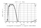
- FIG. 4 is a diagram showing spectral transmittance curves of the resin film of Example 1-1 and the resin film of Example 1-2.
- FIG. 5 is a diagram showing spectral reflectance curves of the dielectric multilayer film (II) of Example 3-3 and the dielectric multilayer film (II) of Example 3-4.
- FIG. 6 shows the spectral transmittance curves of the optical filter of Example 4-1 at incident angles of 0 degrees and 40 degrees, and the spectral reflectance curves at an incident angle of 5 degrees with the incident direction being the dielectric multilayer film (I) side.
- FIG. 4 is a diagram showing;
- FIG. 7 is a diagram showing a spectral reflectance curve of the optical filter of Example 4-1 at an incident angle of 40 degrees with the incident direction facing the dielectric multilayer film (II).
- FIG. 8 shows the spectral transmittance curves of the optical filter of Example 4-2 at incident angles of 0 degrees and 40 degrees, and the spectral reflectance curves at an incident angle of 5 degrees with the incident direction being the dielectric multilayer film (I) side.
- FIG. 4 is a diagram showing;
- FIG. 9 is a diagram showing a spectral reflectance curve of the optical filter of Example 4-2 at an incident angle of 40 degrees with the incident direction facing the dielectric multilayer film (II).
- the near-infrared absorbing dye is sometimes abbreviated as "NIR dye”
- the ultraviolet absorbing dye is sometimes abbreviated as "UV dye”.
- NIR dye the near-infrared absorbing dye
- UV dye ultraviolet absorbing dye
- the compound represented by formula (I) is referred to as compound (I).
- a dye comprising compound (I) is also referred to as dye (I), and the same applies to other dyes.
- the group represented by formula (I) is also referred to as group (I), and the groups represented by other formulas are the same.
- the internal transmittance is expressed by the formula ⁇ measured transmittance (incidence angle of 0 degrees)/(100 ⁇ reflectance (incidence angle of 5 degrees)) ⁇ 100. This is the transmittance obtained by subtracting the influence.
- the spectroscopy of the transmittance of the resin film including the transmittance of the base material and the case where the dye is contained in the resin is all "internal transmittance" even if it is described as "transmittance”.
- the transmittance of the dielectric multilayer film and the transmittance of the optical filter having the dielectric multilayer film are actually measured transmittances.
- a transmittance of, for example, 90% or more in a specific wavelength range means that the transmittance in the entire wavelength range does not fall below 90%, that is, the minimum transmittance in the wavelength range is 90% or more.
- a transmittance of, for example, 1% or less means that the transmittance does not exceed 1% in the entire wavelength range, that is, the maximum transmittance in the wavelength range is 1% or less.
- the average transmittance and average internal transmittance in a particular wavelength range are the arithmetic mean of the transmittance and internal transmittance for each 1 nm of the wavelength range.
- Spectral properties can be measured using a UV-visible spectrophotometer.
- the numerical range "to" includes upper and lower limits.
- An optical filter according to an embodiment of the present invention (hereinafter also referred to as “this filter”) comprises a base material, a dielectric multilayer film 1 laminated as an outermost layer on one main surface side of the base material, and A dielectric multilayer film 2 laminated as an outermost layer is provided on the other main surface side.
- the substrate has near-infrared absorbing glass and a resin film laminated on at least one main surface of the near-infrared absorbing glass.
- the resin film contains a resin and a dye (NIR1) having a maximum absorption wavelength of 680 to 870 nm in the resin.
- the optical filter as a whole Due to the reflection properties of the dielectric multilayer film and the absorption properties of the near-infrared absorbing glass and near-infrared absorbing dye base material, the optical filter as a whole has excellent transmittance in the visible light region and excellent shielding in the near-infrared region. can achieve
- FIG. 1 and 2 are cross-sectional views schematically showing an example of an optical filter according to one embodiment.
- the optical filter 1A shown in FIG. 1 has a dielectric multilayer film 20I on one main surface side of a substrate 10 having a near-infrared absorbing glass 11 and a resin film 12, that is, on the near-infrared absorbing glass 11 in FIG. , the dielectric multilayer film 20II on the other main surface side, that is, on the resin film 12 in FIG.
- “having a specific layer on the main surface side of the base material” is not limited to the case where the layer is provided in contact with the main surface of the base material, and another function is provided between the base material and the layer. Including cases where layers are provided.
- the optical filter 1B shown in FIG. 2 is an example in which the base material 10 has resin films 12A and 12B on both main surfaces of the near-infrared absorbing glass 11, and dielectric multilayer films 20I and 20II on both main surfaces of the base material 10. is.
- the optical filter of the present invention satisfies all of the following spectral characteristics (i-1) to (i-8).
- i-1 In the spectral transmittance curve at an incident angle of 0 degrees, the average transmittance T 440-600 (0 deg) AVE at a wavelength of 440 to 600 nm is 86% or more
- i-2) Spectral transmission at an incident angle of 0 degrees
- the wavelength IR50 (0 deg) T at which the transmittance is 50% in the wavelength range of 550 to 750 nm, and the spectral transmittance curve at the incident angle of 40 degrees the transmittance is 50% in the wavelength range of 550 to 750 nm.
- the absolute value of the difference from the wavelength IR50 (40 deg) T is 6 nm or less (i-3)
- the average transmittance T 700-800 (0 deg) at a wavelength of 700 to 800 nm AVE is 1% or less
- Average transmittance T 800-1200 (0 deg) AVE is 3% or less at a wavelength of 800 to 1200 nm in the spectral transmittance curve at an incident angle of 0 degree (i-5)
- the dielectric Average reflectance RI 440-600 (5 deg) AVE at a wavelength of 440 to 600 nm in the spectral reflectance curve at an incident angle of 5 degrees when the multilayer film (I) side is the incident direction is 4% or less (i-6)
- the average reflectance RI 800-1200 is a wavelength of 800 to
- the optical filter of the present invention reflects near-infrared light on one main surface side of the optical filter, ie, the dielectric multilayer film (I) side, as shown in the characteristic (i-6), while the characteristic (i-6) reflects near-infrared light. As shown in 7), the reflection of near-infrared light is suppressed on the other main surface side, that is, on the side of the dielectric multilayer film (II). As shown in FIG. 3, the incident light L 0 is transmitted through the optical filter 1A, and part of it is reflected on one main surface Sa of the sensor S (reflected light L 1 ).
- the reflected light L1 is reflected (reflected light L2 ) on the back surface of the optical filter, that is, the main surface 20IIb of the dielectric multilayer film 20II (reflected light L2 ). can occur.
- the optical filter of the present invention is also excellent in transmittance in the visible light region and shielding property in the near-infrared light region even at high incident angles, as shown in properties (i-1) to (i-4). Each characteristic will be described in detail below.
- spectral characteristics (i-1) means having excellent transmittance in the visible light region.
- Average transmittance T 440-600 (0 deg) AVE is preferably 88% or more, more preferably 90% or more.
- a dielectric multilayer film with a low visible light reflectance is used.
- the spectral transmittance curve in the region of 550 to 750 nm is less likely to shift even at high incident angles.
- the absolute value of the spectral characteristic (i-2) is preferably 3-5 nm, more preferably 3-4 nm.
- the wavelength region of 600 to 700 nm is shielded by the absorption characteristics of the NIR dye.
- the transmittance tends to decrease due to the absorption of the dyes in the visible light region of 440 to 600 nm. Therefore, among dyes having a squarylium structure, which will be described later, it is preferable to select a dye according to a desired light-shielding band.
- Satisfying the spectral characteristics (i-3) means having excellent light-shielding properties in the near-infrared region from 700 to 800 nm.
- the average transmittance T 700-800 (0 deg) AVE is preferably 0.3% or less, more preferably 0.15% or less.
- a dye capable of absorbing light of 700 to 800 nm may be used.
- Satisfying the spectral characteristics (i-4) means having excellent light-shielding properties in the near-infrared region from 800 to 1200 nm.
- the average transmittance T 800-1200 (0 deg) AVE is preferably 1% or less, more preferably 0.5% or less.
- increasing the near-infrared reflectance of one of the dielectric multilayer films and using near-infrared absorbing glass can be mentioned.
- Satisfying the spectral characteristics (i-5) means having excellent transmittance in the visible light region.
- the average reflectance RI 440-600 (5 deg) AVE is preferably 3% or less, more preferably 1.5% or less.
- designing the dielectric multilayer film (I) to have a small visible light reflectance is exemplified.
- spectral characteristics (i-6) means excellent light-shielding properties in the near-infrared region from 800 to 1200 nm.
- Average reflectance RI 800-1200 (5 deg) AVE is preferably 97% or more, more preferably 98% or more.
- the dielectric multilayer film (I) should be designed to have a high near-infrared light reflectance.
- the spectral characteristics (i-7) means that the reflectance of 700 to 800 nm in the near-infrared region is small even at a high incident angle.
- the average reflectance RII 700-800 (40 deg) AVE is preferably 3% or less, more preferably 2% or less.
- the dielectric multilayer film (II) should be designed to have a small reflectance at 700 to 800 nm.
- the spectral characteristic (i-8) means a range in which reflection of 800 to 1200 nm in the near-infrared region is allowed at a high incident angle.
- Average reflectance RII 800-1200 (40 deg) AVE is preferably 20% or more, more preferably 30% or more.
- the dielectric multilayer film (II) should be designed to have a high reflectance in the range of 800 to 1200 nm.
- the optical filter of the present invention preferably further satisfies the following spectral characteristics (i-9) to (i-10).
- i-9) When the dielectric multilayer film (II) side is the incident direction, the average reflectance RII 700-800 (50 deg) AVE at a wavelength of 700-800 nm in the spectral reflectance curve at an incident angle of 50 degrees is 8% or less (i-10) Average reflectance RII 800-1200 (50 deg ) AVE is 10% or more
- the average reflectance RII 700-800 (50 deg) AVE is preferably 5% or less, more preferably 4% or less.
- the spectral characteristic (i-10) means the range in which reflection of 800 to 1200 nm in the near-infrared region is allowed at higher incident angles.
- Average reflectance RII 800-1200 (50 deg) AVE is preferably 20% or more, more preferably 30% or more.
- the optical filter of the present invention preferably further satisfies the following spectral characteristics (i-12).
- i-12 In the spectral transmittance curve at an incident angle of 0 degrees, the wavelength at which the transmittance is 50% in the wavelength range of 550 to 750 nm is defined as IR50 (0 deg) T ,
- IR50 (5 deg)R is the wavelength at which the reflectance is 50% in the wavelength range of 550 to 750 nm in the spectral reflectance curve at an incident angle of 5 degrees.
- the absolute value of the difference between IR50 (0 deg) T and IR50 (5 deg) R is 85 nm or more
- the spectral characteristic (i-12) defines the relationship between the transmittance and reflectance when incident from the dielectric multilayer film (I) side, and is the wavelength position (IR50 (0 deg) T ) means that the wavelength position (IR50 (5deg)R ) at which the reflectance is 50% is sufficiently far on the longer wavelength side.
- the incident light L 0 is transmitted through the optical filter 1A, and part of it is reflected on one main surface Sa of the sensor S (reflected light L 3 ).
- the reflected light L3 reenters the optical filter 1A and is reflected on the inner surface 20Ib of the dielectric multilayer film 20I (reflected light L4 ).
- Re-incidence of the reflected light L4 to the sensor S can also cause flare and ghost in the same manner as the reflected light L2 .
- the internal reflection of the dielectric multilayer film 20I with a wavelength of 550 to 750 nm can be suppressed, and flare and ghost can be suppressed.
- the IR50 (5 deg)R is sufficiently away from the long wavelength side, the light shielding property at 700 to 800 nm can be supplemented by the absorption properties of the near-infrared absorption dye rather than the reflection properties.
- the IR50 (0 deg)T is preferably in the range of 615-670 nm.
- the IR50 (5 deg)R is preferably in the range of 700-750 nm.
- the absolute value of the difference between IR50 (0 deg) T and IR50 (5 deg) R is more preferably 85 nm or more.
- the dielectric multilayer film is laminated as the outermost layer on both main surface sides of the substrate.
- the dielectric multilayer film (I) is laminated on one main surface side of the substrate, and the dielectric multilayer film (II) is laminated on the other main surface side of the substrate.
- the dielectric multilayer film (I) preferably satisfies all of the following spectral characteristics (vI-1) to (vI-4).
- (vI-1) Average reflectance RI 440-600 (5 deg) AVE is 10% or less at a wavelength of 440 to 600 nm in the spectral reflectance curve at an incident angle of 5 degrees (vI-2) Incident angle of 5 degrees In the spectral reflectance curve at a wavelength of 800 to 1200 nm, the average reflectance RI 800-1200 (5 deg) AVE is 95% or more (v-I-3).
- Average reflectance RI 440-600 (40 deg) at 600 nm AVE is 11% or less (vI-4) Average reflectance RI 800-1200 (40 deg ) AVE is 88% or more
- spectral characteristics (vI-1) means having excellent transmittance in the visible light region.
- Average reflectance RI 440-600 (5 deg) AVE is preferably 8% or less, more preferably 6% or less.
- spectral characteristics (vI-2) means having excellent reflection characteristics for near-infrared light of 800 to 1200 nm.
- Average reflectance RI 800-1200 (5 deg) AVE is preferably 96% or more, more preferably 98% or more.
- the average reflectance RI 440-600 (40 deg) AVE is preferably 10% or less, more preferably 9% or less.
- spectral characteristics means excellent reflection characteristics for near-infrared light of 800 to 1200 nm even at high incident angles.
- Average reflectance RI 800-1200 (40 deg) AVE is preferably 89% or more, more preferably 90% or more.
- the optical filter has the spectral characteristics (i-5) and the spectral characteristics (i -6) is easily satisfied.
- the dielectric multilayer film (I) functions as a reflective film that mainly reflects near-infrared light as described above.
- the dielectric multilayer film (II) preferably satisfies all of the following spectral characteristics (v-II-1) to (v-II-2).
- v-II-1 In the spectral reflectance curve at an incident angle of 5 degrees, the maximum reflectance RII 700-800 (5 deg) MAX at a wavelength of 700 to 800 nm is 8% or less
- v-II-2) Incident angle of 5 degrees
- the average reflectance RII 700-800 (5 deg) AVE at a wavelength of 700-800 nm is 6% or less
- the spectral characteristics (v-II-1) and the spectral characteristics (v-II-2) means that the reflectance at wavelengths of 700 to 800 nm is low.
- the optical filter By designing the dielectric multilayer film (II) to have a small reflectance at a wavelength of 700 to 800 nm, the optical filter easily satisfies the spectral characteristics (i-7).
- the maximum reflectance RII 700-800 (5deg) MAX is preferably 7.5% or less, more preferably 6% or less.
- the average reflectance RII 700-800 (5 deg) AVE is preferably 5.5% or less, more preferably 5% or less.
- the dielectric multilayer film (II) preferably further satisfies the following spectral characteristics (v-II-5).
- v-II-5 spectral characteristics
- v-II-5 In the spectral reflectance curve at an incident angle of 5 degrees, the average reflectance RII 800-1200 (5 deg) AVE at a wavelength of 800 to 1200 nm is 20% or more
- spectral characteristics means having high reflectance at wavelengths of 800 to 1200 nm.
- Average reflectance RII 800-1200 (5 deg) AVE is preferably 27% or more, more preferably 25% or more.
- the dielectric multilayer film (II) preferably further satisfies the following spectral characteristics (v-II-6).
- v-II-6 spectral characteristics
- the average reflectance RII 440-600 (5 deg) AVE at a wavelength of 440 to 600 nm is 6% or less
- v-II-6 means having excellent transmittance in the visible light region.
- the average reflectance RII 440-600 (5 deg) AVE is more preferably 5% or less.
- the spectral characteristics of the dielectric multilayer film (I) and the dielectric multilayer film (II) are obtained by measuring the reflectance of each dielectric multilayer film formed on a transparent glass substrate.
- the dielectric multilayer film (I) is designed as a near-infrared light reflective layer (hereinafter also referred to as an NIR reflective layer), and the dielectric multilayer film (II) is a near-infrared light antireflection layer (hereinafter , also referred to as the NIR antireflection layer).
- the NIR reflective layer and the NIR antireflection layer are composed of, for example, a dielectric multilayer film in which dielectric films with different refractive indices are alternately laminated.
- the dielectric film includes a dielectric film with a low refractive index (low refractive index film) and a dielectric film with a high refractive index (high refractive index film), and these are preferably alternately laminated.
- the high refractive index film preferably has a refractive index of 1.6 or more, more preferably 2.2 to 2.5.
- materials for the high refractive index film include Ta 2 O 5 , TiO 2 and Nb 2 O 5 .
- TiO 2 is preferable from the viewpoints of film formability, reproducibility in refractive index and stability, and the like.
- the low refractive index film preferably has a refractive index of less than 1.6, more preferably 1.4 or more and 1.5 or less.
- materials for the low refractive index film include SiO 2 and SiO x N y .
- SiO 2 is preferred in terms of reproducibility in film formation, stability, economy, and the like.
- the total number of laminated dielectric multilayer films is preferably 20 layers or more, more preferably 30 layers or more, and still more preferably 40 layers or more. , preferably 60 layers or less. Further, the film thickness of the NIR reflective layer is preferably 3 to 6 ⁇ m as a whole.
- the total number of laminated dielectric multilayer films is preferably 30 layers or less, more preferably 25 layers or less, still more preferably 20 layers or less, and more preferably 4 layers or more. Further, the thickness of the NIR antireflection layer is preferably 0.1 to 2 ⁇ m as a whole.
- a vacuum film formation process such as a CVD method, a sputtering method, or a vacuum deposition method, or a wet film formation process such as a spray method or a dip method can be used.
- the dielectric multilayer film may provide predetermined optical characteristics with one layer (one group of dielectric multilayer films), or may provide predetermined optical characteristics with two or more layers. When having two or more layers, each dielectric multilayer film may have the same structure or a different structure.
- the dielectric multilayer film (I) and the dielectric multilayer film (II) may be laminated on either main surface of the substrate, but usually the dielectric multilayer film (I) is laminated on the near-infrared absorbing glass side. , the dielectric multilayer film (II) is preferably laminated on the resin film side. Since the dielectric multilayer film (II) that functions as an antireflection layer is generally smaller in number and thickness than the dielectric multilayer film (I) that functions as a reflective layer, the stress applied to the resin film is reduced. can. When the stress applied to the resin film is small, the resin film is less likely to wrinkle even when the resin is softened under high temperature and high humidity conditions, so reliability can be improved.
- the dielectric multilayer film (I), which is the NIR reflective layer, should be placed on the lens side
- the dielectric multilayer film (II), which is the NIR antireflection layer should be placed on the sensor side. do.
- the substrate has near-infrared absorbing glass and a resin film.
- the resin film contains a resin and a dye (NIR1) having a maximum absorption wavelength of 680 to 870 nm in the resin, and is laminated on at least one main surface of the near-infrared absorbing glass.
- the base material has both the absorption ability of the near-infrared absorption glass and the absorption ability of the resin film containing the near-infrared absorption dye (NIR1).
- the near-infrared absorbing glass preferably satisfies all of the following spectral characteristics (iii-1) to (iii-3).
- iii-2) Average internal transmittance T 700-800 AVE at wavelength 700-800 nm is 40% or less
- (iii-3) Wavelength Average internal transmittance T 800-1200AVE from 800 to 1200 nm is 40% or less
- Satisfying the spectral characteristics (iii-1) means having excellent transmittance in the visible light region of 400 to 600 nm.
- the average internal transmittance T 400-600 AVE is more preferably 92% or higher, still more preferably 95% or higher.
- Satisfying the spectral characteristics (iii-2) means having excellent light-shielding properties in the near-infrared region of 700 to 800 nm.
- the average internal transmittance T 700-800AVE is more preferably 30% or less, still more preferably 25% or less.
- Satisfying the spectral characteristics (iii-3) means having excellent light shielding properties in the near-infrared region of 800 to 1200 nm.
- the average internal transmittance T 800-1200AVE is more preferably 30% or less, still more preferably 25% or less.
- the near-infrared absorption glass is not limited as long as it can obtain the above spectral characteristics, and examples thereof include absorption type glass containing copper ions in fluorophosphate-based glass, phosphate-based glass, and the like.
- phosphate-based glass also includes silicate phosphate glass in which a part of the skeleton of the glass is composed of SiO 2 .
- alkali metal ions with a small ionic radius e.g., Li ions and Na ions
- Chemically strengthened glass obtained by exchanging large alkali ions for example, Na ions or K ions for Li ions, and K ions for Na ions may be used.
- the thickness of the near-infrared absorbing glass is preferably 0.5 mm or less, more preferably 0.3 mm or less from the viewpoint of reducing the height of the camera module, and preferably 0.15 mm or more from the viewpoint of device strength.
- the resin film preferably satisfies all of the following spectral characteristics (iv-1) to (iv-3).
- Satisfying the spectral characteristics (iv-1) means having excellent visible light transmittance of 440 to 600 nm.
- the average internal transmittance T 440-600AVE is more preferably 93% or higher, and still more preferably 95% or higher.
- use of an NIR dye having small absorption characteristics in the visible light region and reduction of the content of the NIR dye can be mentioned.
- Satisfying the spectral characteristics (iv-2) means excellent light shielding properties against near-infrared light with a wavelength of 700 to 800 nm.
- the average internal transmittance T 700-800AVE is more preferably 45% or less, still more preferably 20% or less.
- an NIR dye having a maximum absorption wavelength of 700 to 800 nm may be used.
- spectral characteristics (iv-3) means that a wide range of near-infrared light with a wavelength of 600 to 800 nm can be blocked.
- IR50 (L) -IR50 (S) is more preferably 105 nm or more, still more preferably 110 nm or more.
- IR50 (L) is preferably between 720 and 810 nm and IR50 (S) is preferably between 620 and 670 nm.
- two or more NIR dyes may be used.
- the resin film in the present invention contains a dye (NIR1) having a maximum absorption wavelength of 680 to 870 nm, so that it has excellent light-shielding properties against near-infrared light of 700 to 800 nm as shown in the above characteristic (iv-2). As shown in the above property (iv-3), it is particularly excellent in light-shielding properties over a wide range of near-infrared light from 600 to 800 nm. As a result, the reflection characteristics of the dielectric multilayer film (I) and the dielectric multilayer film (II) at 700 to 800 nm are suppressed in order to reduce flare and ghost, and the absorption characteristics of the NIR dye can be compensated for. As a whole, it is possible to achieve both suppression of flare and ghost and shielding of near-infrared light.
- NIR1 dye having a maximum absorption wavelength of 680 to 870 nm
- the dye (NIR1) has a maximum absorption wavelength in the resin between 680 and 870 nm, preferably between 700 and 730 nm.
- the resin refers to the resin forming the resin film.
- the NIR dye may consist of one kind of compound or may contain two or more kinds of compounds.
- the resin film in the present invention preferably further contains other near-infrared absorbing dyes having different maximum absorption wavelengths in addition to the dye (NIR1). As a result, a wide range of light shielding properties in the near-infrared region around 700 nm can be obtained, and the resin film easily satisfies the characteristic (iv-3).
- a dye (NIR2) having a maximum absorption wavelength in the resin that is 30 to 130 nm longer than that of the dye (NIR1) is preferable. Further, the dye (NIR2) preferably has a maximum absorption wavelength of 740 to 870 nm.
- the dye (NIR1) includes squarylium compounds and phthalocyanine compounds from the viewpoints of maximum absorption wavelength region, visible light transmittance, solubility in resins, and durability, with squarylium compounds being particularly preferred.
- the maximum absorption wavelength of the squarylium compound that is the dye (NIR1) is preferably 680 to 740 nm.
- As the dye (NIR2) a squarylium compound and a cyanine compound are preferable from the viewpoints of maximum absorption wavelength range, visible light transmittance, solubility in resin, and durability.
- the maximum absorption wavelength of the squarylium compound, which is the dye (NIR2) is preferably 740 to 770 nm.
- the maximum absorption wavelength of the cyanine compound that is the dye (NIR2) is preferably 740 to 860 nm.
- ⁇ NIR1 squarylium compound>
- those symbols may be the same or different. The same applies to cyanine compounds.
- R 21 and R 22 , R 22 and R 25 , and R 21 and R 23 are linked together to form 5- or 6-membered heterocyclic ring A, heterocyclic ring B, and heterocyclic ring C, respectively, with the nitrogen atom; good too.
- R 21 and R 22 are, as the divalent group -Q- to which they are bonded, a hydrogen atom having 1 to 6 carbon atoms, an alkyl group having 1 to 6 carbon atoms, an aryl group having 6 to 10 carbon atoms, or It represents an alkylene group optionally substituted by an optionally substituted acyloxy group having 1 to 10 carbon atoms, or an alkyleneoxy group.
- R 22 and R 25 when the heterocyclic ring B is formed, and R 21 and R 23 when the heterocyclic ring C is formed are respectively the divalent groups —X 1 —Y 1 — and — to which they are attached.
- X 2 -Y 2 - (X 1 and X 2 are on the nitrogen-bonding side)
- X 1 and X 2 are groups represented by the following formula (1x) or (2x)
- Y 1 and Y 2 are each A group represented by any one of the following formulas (1y) to (5y).
- each of X 1 and X 2 is a group represented by the following formula (2x)
- each of Y 1 and Y 2 may be a single bond, in which case an oxygen atom may be present between the carbon atoms. .
- Zs are each independently a hydrogen atom, a hydroxyl group, an alkyl group having 1 to 6 carbon atoms or an alkoxy group, or -NR 38 R 39 (R 38 and R 39 are each independently represents a hydrogen atom or an alkyl group having 1 to 20 carbon atoms).
- R 31 to R 36 each independently represent a hydrogen atom, an alkyl group having 1 to 6 carbon atoms or an aryl group having 6 to 10 carbon atoms, and R 37 represents an alkyl group having 1 to 6 carbon atoms or a represents an aryl group.
- R 27 , R 28 , R 29 , R 31 to R 37 , R 21 to R 23 when not forming a heterocyclic ring, and R 25 are combined with any other of these to form a 5- membered ring Or you may form a 6-membered ring.
- R 31 and R 36 and R 31 and R 37 may be directly bonded.
- R 21 , R 22 , R 23 and R 25 when not forming a heterocyclic ring are each independently a hydrogen atom, a halogen atom, a hydroxyl group, an alkyl or alkoxy group having 1 to 20 carbon atoms, or 1 to 10 acyloxy groups, 6 to 11 carbon atoms aryl groups, or optionally substituted and optionally having oxygen atoms between carbon atoms 7 to 18 araryl groups .
- Examples of the compound (I) include compounds represented by any one of formulas (I-1) to (I-3), and solubility in resins, heat resistance and light resistance in resins, From the viewpoint of the visible light transmittance of the contained resin layer, the compound represented by formula (I-1) is particularly preferred.
- X 1 is preferably group (2x), and Y 1 is preferably a single bond or group (1y).
- R 31 to R 36 are preferably a hydrogen atom or an alkyl group having 1 to 3 carbon atoms, more preferably a hydrogen atom or a methyl group.
- -Y 1 -X 1 - specifically includes divalent organic groups represented by formulas (11-1) to (12-3).
- R 21 is independently represented by the formula (Groups represented by 4-1) or (4-2) are more preferred.
- R 71 to R 75 each independently represent a hydrogen atom, a halogen atom, or an alkyl group having 1 to 4 carbon atoms.
- R 24 is preferably —NR 27 R 28 .
- a compound (I-1) in which R 24 is —NH—C( ⁇ O)—R 29 is represented by formula (I-11).
- R 23 and R 26 are each preferably a hydrogen atom, a halogen atom, or an alkyl group or alkoxy group having 1 to 6 carbon atoms, each of which is more preferably a hydrogen atom.
- R 29 is an optionally substituted C 1-20 alkyl group, an optionally substituted C 6-10 aryl group, or an optionally substituted C 6-10
- An araryl group having 7 to 18 carbon atoms which may have an oxygen atom between carbon atoms is preferred.
- substituents include hydroxyl group, carboxy group, sulfo group, cyano group, alkyl group having 1 to 6 carbon atoms, fluoroalkyl group having 1 to 6 carbon atoms, alkoxy group having 1 to 6 carbon atoms, and alkoxy group having 1 to 6 carbon atoms.
- An acyloxy group and the like can be mentioned.
- R 29 is a linear, branched or cyclic alkyl group having 1 to 17 carbon atoms, a phenyl group optionally substituted with an alkoxy group having 1 to 6 carbon atoms, and an oxygen atom between carbon atoms.
- a group selected from araryl groups having 7 to 18 carbon atoms which may be substituted is preferred.
- one or more hydrogen atoms may be independently substituted with a hydroxyl group, a carboxy group, a sulfo group, or a cyano group, and an unsaturated bond between carbon atoms, an oxygen atom, a saturated or unsaturated
- a group which is a hydrocarbon group having at least one or more branches and having 5 to 25 carbon atoms and which may contain a ring structure can also be preferably used.
- Compound (I-11) more specifically includes the compounds shown in the table below.
- the symbols on the left and right sides of the squarylium skeleton have the same meaning.
- the compound (I-11) among these, compounds (1-11-1) to (1-11-12) and compounds (1-11-17) to (1-11-28) are added to the resin From the viewpoint of solubility, maximum absorption wavelength, light resistance, heat resistance, and high absorbance, especially compounds (1-11-1) to (1-11-12) are light resistance and heat resistance. is preferred.
- the dielectric multilayer film has a moderate light-shielding property in the ultraviolet region, so the lightfastness of the dye is particularly important.
- the squarylium compound that is the dye (NIR2) is preferably a compound represented by the following formula (II).
- Each ring Z is independently a 5- or 6-membered ring having 0 to 3 heteroatoms in the ring, and the hydrogen atoms of ring Z may be substituted.
- the carbon atoms or heteroatoms constituting R 1 and R 2 , R 2 and R 3 , and R 1 and ring Z are linked together to form heterocycle A1, heterocycle B1 and heterocycle C1 together with the nitrogen atom, respectively. in which case the hydrogen atoms of heterocycle A1, heterocycle B1 and heterocycle C1 may be substituted.
- R 1 and R 2 when not forming a hetero ring each independently contain a hydrogen atom, a halogen atom, or an unsaturated bond between carbon atoms, a hetero atom, or a saturated or unsaturated ring structure It often represents a hydrocarbon group which may have a substituent.
- R 4 and R 3 when not forming a hetero ring are each independently a hydrogen atom, a halogen atom, or an optionally substituted alkyl group or Indicates an alkoxy group.
- Examples of compound (II) include compounds represented by any one of formulas (II-1) to (II-3). From the viewpoint of solubility in resins and visible light transmission in resins, Compounds of formula (II-3) are particularly preferred.
- R 1 and R 2 each independently represent a hydrogen atom, a halogen atom, or an optionally substituted alkyl group having 1 to 15 carbon atoms.
- R 3 to R 6 each independently represent a hydrogen atom, a halogen atom, or an optionally substituted alkyl group having 1 to 10 carbon atoms.
- R 1 , R 4 , and R 9 to R 12 each independently represent a hydrogen atom, a halogen atom, or an optionally substituted alkyl group having 1 to 15 carbon atoms.
- R 7 and R 8 each independently represent a hydrogen atom, a halogen atom, or an optionally substituted alkyl group having 1 to 5 carbon atoms.
- R 1 and R 2 in compound (II-1) and compound (II-2) are preferably independently alkyl groups having 1 to 15 carbon atoms from the viewpoint of solubility in resins, visible light transmittance, etc. , more preferably an alkyl group having 7 to 15 carbon atoms, at least one of R 1 and R 2 more preferably a branched alkyl group having 7 to 15 carbon atoms, and both R 1 and R 2 having 8 carbon atoms Alkyl groups with ⁇ 15 branches are particularly preferred.
- R 1 in the compound (II-3) is independently preferably an alkyl group having 1 to 15 carbon atoms, and an alkyl group having 1 to 10 carbon atoms, from the viewpoint of solubility in transparent resins, visible light transmittance, etc. is more preferred, and an ethyl group and an isopropyl group are particularly preferred.
- R 4 is preferably a hydrogen atom or a halogen atom, particularly preferably a hydrogen atom, from the viewpoint of visible light transmittance and ease of synthesis.
- R 7 and R 8 are each preferably a hydrogen atom, a halogen atom, or an optionally halogen-substituted alkyl group having 1 to 5 carbon atoms, more preferably a hydrogen atom, a halogen atom, or a methyl group.
- R 9 to R 12 is preferably independently a hydrogen atom, a halogen atom, or an alkyl group having 1 to 5 carbon atoms which may be substituted with a halogen atom.
- —CR 9 R 10 —CR 11 R 12 — includes divalent organic groups represented by the following groups (13-1) to (13-5).
- Compound (II-3) more specifically includes the compounds shown in the table below.
- the symbols on the left and right sides of the squarylium skeleton have the same meaning.
- compounds (II-3) among these, compounds (II-3-1) to (II-3-4) have solubility in resin, high absorption coefficient, light resistance, and heat resistance. preferred from
- Compounds (I) to (II) can be produced by known methods.
- Compound (I) can be produced by the methods described in US Pat.
- Compound (II) can be produced by the method described in International Publication No. 2017/135359.
- cyanine compound is preferably a compound represented by the following formula (III) or a compound represented by the formula (IV).
- R 101 to R 109 and R 121 to R 131 each independently represent a hydrogen atom, a halogen atom, an optionally substituted alkyl group having 1 to 15 carbon atoms, or an aryl group having 5 to 20 carbon atoms.
- R 110 to R 114 and R 132 to R 136 each independently represent a hydrogen atom, a halogen atom or an alkyl group having 1 to 15 carbon atoms.
- X- represents a monovalent anion.
- n1 and n2 are 0 or 1;
- a hydrogen atom bonded to a carbocyclic ring containing -(CH 2 ) n1 - and a carbocyclic ring containing -(CH 2 ) n2 - is a halogen atom, and an optionally substituted alkyl group having 1 to 15 carbon atoms Alternatively, it may be substituted with an aryl group having 5 to 20 carbon atoms.
- the alkyl group (including the alkyl group possessed by the alkoxy group) may be linear, or may contain a branched structure or a saturated ring structure.
- An aryl group refers to a group bonded through a carbon atom constituting an aromatic ring of an aromatic compound, such as a benzene ring, naphthalene ring, biphenyl ring, furan ring, thiophene ring, pyrrole ring, and the like.
- Substituents for optionally substituted alkyl or alkoxy groups having 1 to 15 carbon atoms or aryl groups having 5 to 20 carbon atoms include halogen atoms and alkoxy groups having 1 to 10 carbon atoms. .
- R 101 and R 121 are preferably alkyl groups having 1 to 15 carbon atoms or aryl groups having 5 to 20 carbon atoms, and maintain high visible light transmittance in the resin. From the point of view, a branched alkyl group having 1 to 15 carbon atoms is more preferable.
- R 102 to R 105 , R 108 , R 109 , R 122 to R 127 , R 130 and R 131 are each independently a hydrogen atom, an alkyl group having 1 to 15 carbon atoms, or An alkoxy group or an aryl group having 5 to 20 carbon atoms is preferable, and a hydrogen atom is more preferable from the viewpoint of obtaining high visible light transmittance.
- R 110 to R 114 and R 132 to R 136 are each independently preferably a hydrogen atom or an alkyl group having 1 to 15 carbon atoms, from the viewpoint of obtaining high visible light transmittance.
- a hydrogen atom from is more preferable.
- R 106 , R 107 , R 128 and R 129 are each independently a hydrogen atom, an alkyl group having 1 to 15 carbon atoms, or an aryl group having 5 to 20 carbon atoms (including chain, cyclic and branched alkyl groups). ) is preferable, and a hydrogen atom or an alkyl group having 1 to 15 carbon atoms is more preferable.
- R 106 and R 107 , and R 128 and R 129 are preferably the same group.
- X ⁇ includes I ⁇ , BF 4 ⁇ , PF 6 ⁇ , ClO 4 ⁇ , anions represented by formulas (X1) and (X2), etc., preferably BF 4 ⁇ or PF 6 ⁇ be.
- R 101 to R 114 and X - are the same as in formula (III).
- R 115 to R 120 each independently represent a hydrogen atom, a halogen atom, an optionally substituted alkyl or alkoxy group having 1 to 15 carbon atoms, or an aryl group having 5 to 20 carbon atoms.
- R 115 to R 120 are each independently preferably a hydrogen atom, an alkyl group having 1 to 15 carbon atoms, or an aryl group having 5 to 20 carbon atoms (which may include a chain, cyclic or branched alkyl group), A hydrogen atom or an alkyl group having 1 to 15 carbon atoms is more preferable.
- R 115 to R 120 are preferably the same group.
- R 121 to R 136 and X - are the same as in formula (IV).
- R 137 to R 142 each independently represent a hydrogen atom, a halogen atom, an optionally substituted alkyl or alkoxy group having 1 to 15 carbon atoms, or an aryl group having 5 to 20 carbon atoms.
- R 137 to R 142 are each independently preferably a hydrogen atom, an alkyl group having 1 to 15 carbon atoms, or an aryl group having 5 to 20 carbon atoms (which may include a chain, cyclic, or branched alkyl group); Atoms or alkyl groups having 1 to 15 carbon atoms are more preferred.
- R 137 to R 142 are preferably the same group.
- the compounds represented by formula (III-1), formula (III-2), formula (IV-1), and formula (IV-2) each include an atom bonded to each skeleton or Included are compounds in which the groups are the atoms or groups shown in the table below.
- R 101 to R 109 are all the same on the left and right sides of the formula.
- R 121 -R 131 are the same on the left and right sides of the formula.
- R 110 to R 114 in the table below and R 132 to R 136 in the table below represent atoms or groups bonded to the central benzene ring in each formula, and when all five are hydrogen atoms, they are described as "H".
- R 110 to R 114 is a substituent and the other is a hydrogen atom, only the combination of the symbol of the substituent and the substituent is described.
- R 112 —C(CH 3 ) 3 indicates that R 112 is —C(CH 3 ) 3 and otherwise a hydrogen atom.
- R 132 -R 136 The same applies to R 132 -R 136 .
- R 115 -R 120 in the table below and R 137 -R 142 in the table below represent atoms or groups bonded to the central cyclohexane ring in formula (III-1) and formula (IV-1), all six of which are In the case of a hydrogen atom, it is described as "H".
- R 115 to R 120 is a substituent and the other is a hydrogen atom, only the combination of the symbol of the substituent and the substituent is described. The same applies to R 137 -R 142 .
- R 115 -R 118 in the table below and R 137 -R 140 in the table below represent atoms or groups bonded to the central cyclopentane ring in formula (III-2) and formula (IV-2), and all four is a hydrogen atom, it is described as "H”.
- R 115 to R 118 is a substituent and the other is a hydrogen atom, only the combination of the symbol of the substituent and the substituent is described. The same is true for R 137 -R 140 .
- the dye (III-1) among these, the dyes (III-1-1) to (III-1-12) etc. are used from the viewpoint of heat resistance, light resistance, solubility in resin, and simplicity of synthesis. is preferred.
- the dye (III-2) among these, the dyes (III-2-1) to (III-2-12), etc., are selected from the viewpoints of heat resistance, light resistance, solubility in resins, and simplicity of synthesis. is preferred.
- the dye (IV-1) among these, the dyes (IV-1-1) to (IV-1-12) and the like are used from the viewpoint of heat resistance, light resistance, solubility in resins, and simplicity of synthesis. is preferred.
- dyes (IV-2-1) to (IV-2-15), etc. are selected from the viewpoints of heat resistance, light resistance, solubility in resin, and simplicity of synthesis. is preferred.
- Dye (III) and dye (IV) are described, for example, in Dyes and Pigments 73 (2007) 344-352 and J. Am. It can be produced by the method described in Heterocyclic Chem, 42, 959 (2005).
- the content of the NIR dye in the resin film is preferably 0.1 to 25 parts by mass, more preferably 0.3 to 15 parts by mass, per 100 parts by mass of the resin. In addition, when combining 2 or more types of compounds, the said content is sum total of each compound. Further, when the dye (NIR1) and the dye (NIR2) are used together, the content of the dye (NIR1) is preferably 0.1 to 10 parts by mass with respect to 100 parts by mass of the resin, and the content of the dye (NIR2) is 100 parts by mass of the resin. It is preferably 0.1 to 10 parts by mass.
- the resin film may contain other near-infrared absorbing dyes in addition to the dye (NIR1) and the dye (NIR2).
- the other near-infrared absorbing dye a dye having a maximum absorption wavelength larger than that of the dye (NIR2) is preferable from the viewpoint of being able to shield a wide range of the near-infrared region, and specific examples thereof include cyanine compounds and diimmonium compounds.
- the resin film may contain other dyes in addition to the NIR dyes described above.
- a dye (UV) having a maximum absorption wavelength in the resin of 370 to 440 nm is preferable. Thereby, the near-ultraviolet region can be efficiently shielded.
- Dyes include oxazole dyes, merocyanine dyes, cyanine dyes, naphthalimide dyes, oxadiazole dyes, oxazine dyes, oxazolidine dyes, naphthalic acid dyes, styryl dyes, anthracene dyes, cyclic carbonyl dyes, triazole dyes, and the like. be done.
- merocyanine dyes are particularly preferred.
- one type may be used alone, or two or more types may be used in combination.
- the content of the pigment (UV) in the resin film is preferably 0.1 to 15 parts by mass, more preferably 1 to 10 parts by mass, per 100 parts by mass of the resin. Within this range, deterioration of resin properties is less likely to occur.
- the substrate in this filter is a composite substrate in which a resin film is laminated on at least one main surface of near-infrared absorbing glass.
- Resins are not limited as long as they are transparent resins, and include polyester resins, acrylic resins, epoxy resins, ene-thiol resins, polycarbonate resins, polyether resins, polyarylate resins, polysulfone resins, polyethersulfone resins, and polyparaphenylene.
- One or more transparent resins selected from resins, polyarylene ether phosphine oxide resins, polyamide resins, polyimide resins, polyamideimide resins, polyolefin resins, cyclic olefin resins, polyurethane resins, polystyrene resins, and the like are used. These resins may be used individually by 1 type, and may be used in mixture of 2 or more types.
- One or more resins selected from polyimide resins, polycarbonate resins, polyester resins, and acrylic resins are preferable from the viewpoint of spectral characteristics, glass transition point (Tg), and adhesion of the resin film.
- NIR dyes and other dyes When multiple compounds are used as NIR dyes and other dyes, they may be contained in the same resin film, or may be contained in separate resin films.
- a resin film is prepared by dissolving or dispersing a dye, a resin or a raw material component of the resin, and each component to be blended as necessary in a solvent to prepare a coating solution, coating the solution on a support, and drying it. It can be formed by curing and, if necessary, curing.
- the support in this case may be the near-infrared absorbing glass used in the present filter, or may be a peelable support used only when forming the resin film.
- the solvent may be a dispersion medium capable of stably dispersing or a solvent capable of dissolving.
- the coating liquid may contain a surfactant to improve voids caused by microbubbles, dents caused by adhesion of foreign matter, repellency during the drying process, and the like.
- a surfactant to improve voids caused by microbubbles, dents caused by adhesion of foreign matter, repellency during the drying process, and the like.
- dip coating, cast coating, spin coating, or the like can be used for the application of the coating liquid.
- a resin film is formed by coating the above coating liquid on a support and then drying it.
- the coating liquid contains a raw material component of the transparent resin, it is further subjected to a curing treatment such as heat curing or photocuring.
- the resin film can also be produced in the form of a film by extrusion molding.
- a substrate can be produced by laminating the obtained film-like resin film on a near-infrared absorbing glass and integrating them by thermocompression bonding or the like.
- the resin film may have one layer in the optical filter, or may have two or more layers. When it has two or more layers, each layer may have the same configuration or different configurations.
- the thickness of the resin film is preferably 10 ⁇ m or less, more preferably 5 ⁇ m or less, from the viewpoint of the in-plane film thickness distribution in the substrate after coating and the appearance quality. is preferably 0.5 ⁇ m or more from the viewpoint of expressing the When the optical filter has two or more layers of resin films, the total thickness of each resin film is preferably within the above range.
- the shape of the substrate is not particularly limited, and may be block-shaped, plate-shaped, or film-shaped.
- the present filter may include, as other constituent elements, for example, a constituent element (layer) that provides absorption by inorganic fine particles or the like that controls the transmission and absorption of light in a specific wavelength range.
- a constituent element layer
- inorganic fine particles include ITO (indium tin oxides), ATO (antimony-doped tin oxides), cesium tungstate, and lanthanum boride.
- ITO fine particles and cesium tungstate fine particles have high visible light transmittance and absorb light over a wide range of infrared wavelengths exceeding 1200 nm, so they can be used when such infrared light shielding properties are required. .
- a base material a dielectric multilayer film (I) laminated as an outermost layer on one main surface side of the base material, and a dielectric laminated as an outermost layer on the other main surface side of the base material
- An optical filter comprising a multilayer film (II)
- the substrate comprises near-infrared absorbing glass and a resin film laminated on at least one main surface of the near-infrared absorbing glass
- the resin film contains a resin and a dye (NIR1) having a maximum absorption wavelength of 680 to 870 nm in the resin,
- NIR1 dye having a maximum absorption wavelength of 680 to 870 nm in the resin
- An optical filter that satisfies all of the following spectral characteristics (i-1) to (i-8).
- the average transmittance T 440-600 (0 deg) AVE at a wavelength of 440 to 600 nm is 86% or more
- i-2 Spectral transmission at an incident angle of 0 degrees
- the wavelength IR50 (0 deg) T at which the transmittance is 50% in the wavelength range of 550 to 750 nm, and the spectral transmittance curve at the incident angle of 40 degrees the transmittance is 50% in the wavelength range of 550 to 750 nm.
- the absolute value of the difference from the wavelength IR50 (40 deg) T is 6 nm or less (i-3)
- the average transmittance T 700-800 (0 deg) at a wavelength of 700 to 800 nm AVE is 1% or less
- Average transmittance T 800-1200 (0 deg) AVE is 3% or less at a wavelength of 800 to 1200 nm in the spectral transmittance curve at an incident angle of 0 degree (i-5)
- the dielectric Average reflectance RI 440-600 (5 deg) AVE at a wavelength of 440 to 600 nm in the spectral reflectance curve at an incident angle of 5 degrees when the multilayer film (I) side is the incident direction is 4% or less (i-6)
- the average reflectance RI 800-1200 is a wavelength of 800 to
- the average reflectance RII 700-800 (50 deg) AVE at a wavelength of 700-800 nm in the spectral reflectance curve at an incident angle of 50 degrees is 8% or less
- the dielectric multilayer film (II) is laminated on the resin film according to any one of [1] to [3]. optical filters. [5] The optical filter according to any one of [1] to [4], wherein the dielectric multilayer film (II) satisfies all of the following spectral characteristics (v-II-1) to (v-II-2) .
- the maximum reflectance RII 700-800 (5 deg) MAX at a wavelength of 700 to 800 nm is 8% or less (v-II-2) Incident angle of 5 degrees
- the average reflectance RII 700-800 (5 deg) AVE at a wavelength of 700 to 800 nm is 6% or less [6]
- the dielectric multilayer film (II) has the following spectral characteristics (v-II-3 ) to (v-II-5), the optical filter according to any one of [1] to [5].
- the optical filter has the following spectral characteristics ( The optical filter according to any one of [1] to [7], further satisfying i-12).
- IR50 (0 deg) T
- IR50 (5 deg)R is the wavelength at which the reflectance is 50% in the wavelength range of 550 to 750 nm in the spectral reflectance curve at an incident angle of 5 degrees.
- IR50 (S) is the shortest wavelength at which the internal transmittance is 50%
- IR50 (L) is the longest wavelength
- IR50 (L) - IR50 (S) ⁇ 100 nm
- the resin film has a maximum absorption wavelength of 680 to 870 nm in the resin, and further includes a dye (NIR2) having a maximum absorption wavelength different from that of the dye (NIR1), [1] to [9].
- the optical filter according to any one of 1. [11] An imaging device comprising the optical filter according to any one of [1] to [10].
- the dyes used in each example are as follows.
- Compound NIR1 (squarylium compound): synthesized based on Japanese Patent Application Laid-Open No. 2017-110209.
- Compound NIR2 (squarylium compound): Synthesized based on Japanese Patent Application Laid-Open No. 2017-110209.
- Compound NIR3 (cyanine compound): synthesized based on the method described in Dyes and Pigments, 73, 344-352 (2007).
- Compound NIR4 (squarylium compound) synthesized based on WO2017/135359.
- Compound NIR5 (phthalocyanine compound): synthesized based on the method described in Journal of physical chemistry, C 117(14), 7097-7106, 2013.
- Compound UV1 (merocyanine compound): Synthesized according to German Patent Publication No. 10109243.
- the resulting coating solution was applied to an alkali glass (D263 glass manufactured by SCHOTT, thickness 0.2 mm) by a spin coating method to form a coating film having a thickness of approximately 1.0 ⁇ m.
- the obtained coating film was subjected to transmission spectroscopy (incidence angle of 0 degrees) and reflection spectroscopy (incidence angle of 5 degrees) in a wavelength range of 350 nm to 1200 nm using a spectrophotometer.
- a spectral internal transmittance curve was calculated.
- the following table shows the spectral characteristics of each of the above dyes in a polyimide resin.
- the near-infrared absorbing glass used has a high transmittance in the visible light region and excellent light-shielding properties in the near-infrared light region.
- Spectral characteristics of resin film Any one of the above dyes is mixed with the polyimide resin solution prepared in the same manner as when calculating the spectral characteristics of each dye compound at the concentrations shown in the table below, and then stirred and dissolved at 50 ° C for 2 hours. Got the working fluid.
- the resulting coating liquid was applied to alkali glass (D263 glass manufactured by SCHOTT, thickness 0.2 mm) by a spin coating method to form a resin film having a thickness of 1.0 ⁇ m.
- the obtained resin film was subjected to transmission spectroscopy (incidence angle of 0 degrees) and reflection spectroscopy (incidence angle of 5 degrees) in a wavelength range of 350 nm to 1200 nm using a spectrophotometer. Using the obtained spectral transmittance curve and spectral reflectance curve, a spectral internal transmittance curve was calculated. The obtained spectral characteristics are shown in the table below.
- FIG. 4 shows spectral transmittance curves of the resin film of Example 1-1 and the resin film of Example 1-2. Examples 1-1 to 1-4 are reference examples.
- the obtained resin film has a high transmittance in the visible light region and is excellent in light shielding properties in the near infrared region from 700 to 800 nm. Furthermore, the resin films of Examples 1-2 to 1-4 had a difference of more than 100 nm between IR 50 (L) and IR 50 (S) , and could absorb a wide range of near-infrared light from 700 to 800 nm. I understand.
- Example 2-1 Spectral characteristics of dielectric multilayer film (I)> On the surface of alkali glass (SCHOTT D263 glass, thickness 0.2 mm), TiO 2 and SiO 2 were alternately laminated by vapor deposition under the conditions shown in the table below to form a dielectric multilayer film (I). The obtained dielectric multilayer film was measured for a spectral reflectance curve in a wavelength range of 350 to 1200 nm using an ultraviolet-visible spectrophotometer. The obtained spectral characteristics are shown in the table below. Note that Example 2-1 is a reference example.
- Examples 3-1 to 3-4 Spectral characteristics of dielectric multilayer film (II)> On the surface of alkali glass (SCHOTT D263 glass, thickness 0.2 mm), TiO 2 and SiO 2 were alternately laminated by vapor deposition under the conditions shown in the table below to form a dielectric multilayer film (II). The obtained dielectric multilayer film was measured for a spectral reflectance curve in a wavelength range of 350 to 1200 nm using an ultraviolet-visible spectrophotometer. The obtained spectral characteristics are shown in the table below.
- FIG. 5 shows spectral reflectance curves of the dielectric multilayer film (II) of Example 3-3 and the dielectric multilayer film (II) of Example 3-4. Examples 3-1 to 3-4 are reference examples.
- dielectric multilayer films with particularly low reflectance in the range of 700 to 800 nm were obtained.
- Examples 4-1 to 4-8 Spectral characteristics of optical filters>
- a dielectric multilayer film (I) (reflective film) was deposited on one main surface of the substrate by vapor deposition in the same manner as in Example 2-1. Incidentally, only in Example 4-6, the dielectric multilayer film (I) was formed in the same manner as in Example 3-1.
- a resin film was formed on the other surface of the substrate in the same manner as in any of Examples 1-1 to 1-4. Further, a dielectric multilayer film (II) (antireflection film) was deposited on the resin film by vapor deposition in the same manner as in any one of Examples 3-1 to 3-4 to prepare an optical filter.
- any one of the above absorption glasses 1 to 3 transparent alkali glass (SCHOTT, D263 glass, thickness 0.2 mm), transparent resin film (polycarbonate film, Teijin, Pure Ace, thickness 80 ⁇ m) is used.
- FIG. 6 shows the spectral transmittance curves of the optical filter of Example 4-1 at incident angles of 0 degrees and 40 degrees, and the spectral reflectance curves at an incident angle of 5 degrees with the incident direction on the dielectric multilayer film (I) side. show.
- FIG. 7 shows a spectral reflectance curve of the optical filter of Example 4-1 at an incident angle of 40 degrees with the incident direction being the dielectric multilayer film (II) side.
- FIG. 8 shows the spectral transmittance curves of the optical filter of Example 4-2 at incident angles of 0 degrees and 40 degrees, and the spectral reflectance curves at an incident angle of 5 degrees with the incident direction being the dielectric multilayer film (I) side. show.
- FIG. 9 shows a spectral reflectance curve of the optical filter of Example 4-2 at an incident angle of 40 degrees with the incident direction being the dielectric multilayer film (II) side.
- Examples 4-1 to 4-5 are examples, and examples 4-6 to 4-8 are comparative examples.
- the optical filters of Examples 4-1 to 4-5 have high transmittance in the visible light region and high shielding properties in the near-infrared light region of 700 to 1200 nm. It can be seen that the filter has a low reflectance at an incident angle of 40 degrees for 700 to 800 nm on the film (II) side. Furthermore, Examples 4-4 to 4-5, in which the absolute value of the difference between IR50 (0 deg) T and IR50 (5 deg) R is 85 nm or more, are 700% higher than Examples 4-1 to 4-3. While suppressing the reflection on the back surface at ⁇ 800 nm, the transmittance at 700 to 800 nm can also be suppressed.
- the 700 to 800 nm light-shielding property can be ensured by the absorption of the NIR dye, not by the reflection of the dielectric multilayer film, and can be said to be an optical filter capable of suppressing the generation of stray light due to reflection from the back surface.
- the reflectance at an incident angle of 40 degrees for 700 to 800 nm on the dielectric multilayer film (II) side is not suppressed.
- the optical filters of Examples 4-6 do not use a dielectric multilayer film (II) that satisfies specific spectral characteristics.
- the optical filters of Examples 4-7 use transparent glass as a substrate that does not absorb infrared rays.
- the optical filters of Examples 4-8 do not use a dielectric multilayer film (II) that satisfies specific spectral characteristics.
- the optical filter of the present invention suppresses flares and ghosts, and has spectral characteristics with excellent transmittance in the visible light region and shielding properties in the near-infrared light region. For example, it is useful for use in imaging devices such as cameras and sensors for transport aircraft, which have become highly sophisticated in recent years.
- 1A, 1B optical filter, 10... base material, 11... near-infrared absorbing glass, 12, 12A, 12B... resin film, 20I, 20II... dielectric multilayer film
Landscapes
- Physics & Mathematics (AREA)
- General Physics & Mathematics (AREA)
- Optics & Photonics (AREA)
- Optical Filters (AREA)
- Laminated Bodies (AREA)
Abstract
本発明は、近赤外線吸収ガラスと、樹脂膜と、誘電体多層膜(I)と、誘電体多層膜(II)とを備える光学フィルタであって、前記樹脂膜は680~870nmに最大吸収波長を有する色素を含み、前記光学フィルタが特定の分光特性(i-1)~(i-6)および下記分光特性(i-7)~(i-8)をすべて満たす、光学フィルタに関する。(i-7)入射角40度、波長700~800nmにおける平均反射率が5.5%以下 (i-8)入射角40度、波長800~1200nmにおける平均反射率が10%以上
Description
本発明は、可視光を透過し、近赤外光を遮断する光学フィルタに関する。
固体撮像素子を用いた撮像装置には、色調を良好に再現し鮮明な画像を得るため、可視域の光(以下「可視光」ともいう)を透過し、近赤外波長領域の光(以下「近赤外光」ともいう)を遮断する光学フィルタが用いられる。
このような光学フィルタは、例えば、透明基板の片面または両面に、屈折率が異なる誘電体薄膜を交互に積層(誘電体多層膜)し、光の干渉を利用して遮蔽したい光を反射する反射型のフィルタ等、様々な方式が挙げられる。
特許文献1および2には、誘電体多層膜と、色素を含む吸収層とを有する光学フィルタが記載されている。
光学フィルタを透過した光の大半はセンサ内に入射するが、一部の光はセンサ面で反射し、光学フィルタの裏面側の誘電体多層膜上でさらに反射して、センサ内に再入射することにより、本来想定される光路外に光が発生する現象、いわゆる迷光が生じうる。このような光学フィルタとセンサ間の反復反射による迷光により、固体撮像素子においてフレアやゴーストが生じ、画質が低下するおそれがある。近年のカメラモジュールの高画質化に伴い、フレアやゴーストが生じにくい光学フィルタが求められている。特に700~800nmの波長領域はセンサ感度が高いことから、かかる波長領域におけるフレアやゴーストの抑制が望まれている。
また、誘電体多層膜は光の入射角度により光学膜厚が変化するため反射特性が変化しうることから、高入射角であるほど上記のフレアやゴーストは発生しやすい。特に、近年のカメラモジュール低背化に伴い高入射角条件での使用が想定されるため、入射角の影響を受けにくい光学フィルタが求められている。
本発明は、高入射角であっても、可視光領域の透過性と近赤外光領域の遮蔽性に優れ、フレアやゴーストが抑制された光学フィルタの提供を目的とする。
本発明は、以下の構成を有する光学フィルタ等を提供する。
〔1〕基材と、前記基材の一方の主面側に最外層として積層された誘電体多層膜(I)と、前記基材の他方の主面側に最外層として積層された誘電体多層膜(II)とを備える光学フィルタであって、
前記基材は、近赤外線吸収ガラスと、前記近赤外線吸収ガラスの少なくとも一方の主面に積層された樹脂膜とを有し、
前記樹脂膜は、樹脂と、前記樹脂中で680~870nmに最大吸収波長を有する色素(NIR1)とを含み、
前記光学フィルタが下記分光特性(i-1)~(i-8)をすべて満たす光学フィルタ。
(i-1)入射角0度での分光透過率曲線において、波長440~600nmの平均透過率T440-600(0deg)AVEが86%以上
(i-2)入射角0度での分光透過率曲線において、波長550~750nmの範囲で透過率が50%となる波長IR50(0deg)Tと、入射角40度での分光透過率曲線において、波長550~750nmの範囲で透過率が50%となる波長IR50(40deg)Tとの差の絶対値が、6nm以下
(i-3)入射角0度での分光透過率曲線において、波長700~800nmの平均透過率T700-800(0deg)AVEが1%以下
(i-4)入射角0度での分光透過率曲線において、波長800~1200nmの平均透過率T800-1200(0deg)AVEが3%以下
(i-5)前記誘電体多層膜(I)側を入射方向としたとき、入射角5度での分光反射率曲線において、波長440~600nmにおける平均反射率RI440-600(5deg)AVEが4%以下
(i-6)前記誘電体多層膜(I)側を入射方向としたとき、入射角5度での分光反射率曲線において、波長800~1200nmにおける平均反射率RI800-1200(5deg)AVEが95%以上
(i-7)前記誘電体多層膜(II)側を入射方向としたとき、入射角40度での分光反射率曲線において、波長700~800nmにおける平均反射率RII700-800(40deg)AVEが5.5%以下
(i-8)前記誘電体多層膜(II)側を入射方向としたとき、入射角40度での分光反射率曲線において、波長800~1200nmにおける平均反射率RII800-1200(40deg)AVEが10%以上
本発明によれば、高入射角であっても、可視光領域の透過性と近赤外光領域の遮蔽性に優れ、フレアやゴーストが抑制された光学フィルタが提供できる。
以下、本発明の実施の形態について説明する。
本明細書において、近赤外線吸収色素を「NIR色素」、紫外線吸収色素を「UV色素」と略記することもある。
本明細書において、式(I)で示される化合物を化合物(I)という。他の式で表される化合物も同様である。化合物(I)からなる色素を色素(I)ともいい、他の色素についても同様である。また、式(I)で表される基を基(I)とも記し、他の式で表される基も同様である。
本明細書において、近赤外線吸収色素を「NIR色素」、紫外線吸収色素を「UV色素」と略記することもある。
本明細書において、式(I)で示される化合物を化合物(I)という。他の式で表される化合物も同様である。化合物(I)からなる色素を色素(I)ともいい、他の色素についても同様である。また、式(I)で表される基を基(I)とも記し、他の式で表される基も同様である。
本明細書において、内部透過率とは、{実測透過率(入射角0度)/(100-反射率(入射角5度))}×100の式で示される、実測透過率から界面反射の影響を引いて得られる透過率である。
本明細書において、基材の透過率、色素が樹脂に含有される場合を含む樹脂膜の透過率の分光は、「透過率」と記載されている場合も全て「内部透過率」である。一方、誘電体多層膜の透過率、誘電体多層膜を有する光学フィルタの透過率は、実測透過率である。
本明細書において、基材の透過率、色素が樹脂に含有される場合を含む樹脂膜の透過率の分光は、「透過率」と記載されている場合も全て「内部透過率」である。一方、誘電体多層膜の透過率、誘電体多層膜を有する光学フィルタの透過率は、実測透過率である。
本明細書において、特定の波長域について、透過率が例えば90%以上とは、その全波長領域において透過率が90%を下回らない、すなわちその波長領域において最小透過率が90%以上であることをいう。同様に、特定の波長域について、透過率が例えば1%以下とは、その全波長領域において透過率が1%を超えない、すなわちその波長領域において最大透過率が1%以下であることをいう。内部透過率においても同様である。特定の波長域における平均透過率および平均内部透過率は、該波長域の1nm毎の透過率および内部透過率の相加平均である。
分光特性は、紫外可視分光光度計を用いて測定できる。
本明細書において、数値範囲を表す「~」では、上下限を含む。
分光特性は、紫外可視分光光度計を用いて測定できる。
本明細書において、数値範囲を表す「~」では、上下限を含む。
<光学フィルタ>
本発明の一実施形態の光学フィルタ(以下、「本フィルタ」ともいう)は、基材と、基材の一方の主面側に最外層として積層された誘電体多層膜1と、基材の他方の主面側に最外層として積層された誘電体多層膜2とを備える。
ここで基材は、近赤外線吸収ガラスと、近赤外線吸収ガラスの少なくとも一方の主面に積層された樹脂膜とを有する。さらに樹脂膜は、樹脂と、樹脂中で680~870nmに最大吸収波長を有する色素(NIR1)とを含む。
誘電体多層膜の反射特性と、近赤外線吸収ガラスおよび近赤外線吸収色素を含む基材の吸収特性とにより、光学フィルタ全体として可視光領域の優れた透過性と近赤外光領域の優れた遮蔽性を実現できる。
本発明の一実施形態の光学フィルタ(以下、「本フィルタ」ともいう)は、基材と、基材の一方の主面側に最外層として積層された誘電体多層膜1と、基材の他方の主面側に最外層として積層された誘電体多層膜2とを備える。
ここで基材は、近赤外線吸収ガラスと、近赤外線吸収ガラスの少なくとも一方の主面に積層された樹脂膜とを有する。さらに樹脂膜は、樹脂と、樹脂中で680~870nmに最大吸収波長を有する色素(NIR1)とを含む。
誘電体多層膜の反射特性と、近赤外線吸収ガラスおよび近赤外線吸収色素を含む基材の吸収特性とにより、光学フィルタ全体として可視光領域の優れた透過性と近赤外光領域の優れた遮蔽性を実現できる。
図面を用いて本フィルタの構成例について説明する。図1~2は、一実施形態の光学フィルタの一例を概略的に示す断面図である。
図1に示す光学フィルタ1Aは、近赤外線吸収ガラス11と樹脂膜12とを有する基材10の一方の主面側、すなわち図1では近赤外線吸収ガラス11上に誘電体多層膜20Iを有し、他方の主面側、すなわち図1では樹脂膜12上に誘電体多層膜20IIを有する例である。なお、「基材の主面側に特定の層を有する」とは、基材の主面に接触して該層が備わる場合に限らず、基材と該層との間に、別の機能層が備わる場合も含む。
図2に示す光学フィルタ1Bは、基材10が近赤外線吸収ガラス11の両主面に樹脂膜12A,12Bを有し、基材10の両主面に誘電体多層膜20I,20IIを有する例である。
本発明の光学フィルタは、下記分光特性(i-1)~(i-8)をすべて満たす。
(i-1)入射角0度での分光透過率曲線において、波長440~600nmの平均透過率T440-600(0deg)AVEが86%以上
(i-2)入射角0度での分光透過率曲線において、波長550~750nmの範囲で透過率が50%となる波長IR50(0deg)Tと、入射角40度での分光透過率曲線において、波長550~750nmの範囲で透過率が50%となる波長IR50(40deg)Tとの差の絶対値が、6nm以下
(i-3)入射角0度での分光透過率曲線において、波長700~800nmの平均透過率T700-800(0deg)AVEが1%以下
(i-4)入射角0度での分光透過率曲線において、波長800~1200nmの平均透過率T800-1200(0deg)AVEが3%以下
(i-5)前記誘電体多層膜(I)側を入射方向としたとき、入射角5度での分光反射率曲線において、波長440~600nmにおける平均反射率RI440-600(5deg)AVEが4%以下
(i-6)前記誘電体多層膜(I)側を入射方向としたとき、入射角5度での分光反射率曲線において、波長800~1200nmにおける平均反射率RI800-1200(5deg)AVEが95%以上
(i-7)前記誘電体多層膜(II)側を入射方向としたとき、入射角40度での分光反射率曲線において、波長700~800nmにおける平均反射率RII700-800(40deg)AVEが5.5%以下
(i-8)前記誘電体多層膜(II)側を入射方向としたとき、入射角40度での分光反射率曲線において、波長800~1200nmにおける平均反射率RII800-1200(40deg)AVEが10%以上
本発明の光学フィルタは、特性(i-6)に示すように光学フィルタの一方の主面側、すなわち前記誘電体多層膜(I)側では近赤外光を反射する一方、特性(i-7)に示すように他方の主面側、すなわち前記誘電体多層膜(II)側では近赤外光の反射を抑制する。
図3に示すように、入射光L0は、光学フィルタ1Aを透過し、一部がセンサSの一方の主面Sa上で反射される(反射光L1)。反射光L1は、光学フィルタの裏面、すなわち誘電体多層膜20IIの主面20IIb上で反射され(反射光L2)、この反射光L2がセンサSに再入射することで、フレアやゴーストを発生させうる。近赤外光の反射を抑制する主面側、すなわち誘電体多層膜(II)側をセンサと対向するように光学フィルタを実装すれば、フレアやゴーストの原因となる光学フィルタの裏面反射が抑制できる。
本発明の光学フィルタはまた、特性(i-1)~(i-4)に示すように高入射角であっても可視光領域の透過性と近赤外光領域の遮蔽性に優れる。
以下、各特性について詳述する。
分光特性(i-1)を満たすことは、可視光領域の透過性に優れることを意味する。
平均透過率T440-600(0deg)AVEは好ましくは88%以上、より好ましくは90%以上である。
分光特性(i-1)を満たすためには、例えば、可視光反射率の小さい誘電体多層膜を用いることが挙げられる。
平均透過率T440-600(0deg)AVEは好ましくは88%以上、より好ましくは90%以上である。
分光特性(i-1)を満たすためには、例えば、可視光反射率の小さい誘電体多層膜を用いることが挙げられる。
分光特性(i-2)を満たすことは、高入射角においても550~750nmの領域の分光透過率曲線がシフトしにくいことを意味する。
分光特性(i-2)における絶対値は好ましくは3~5nm、より好ましくは3~4nmである。
分光特性(i-2)を満たすためには、例えば、NIR色素の吸収特性により600~700nmの波長領域を遮光することが挙げられる。ただし、色素の吸収特性を利用する場合、440~600nmの可視光領域も色素が吸収してしまうことにより透過率が低下しやすい。したがって、後述のスクアリリウム構造を有する色素のうち、所望の遮光帯域に合わせて色素を選択することが好ましい。
分光特性(i-2)における絶対値は好ましくは3~5nm、より好ましくは3~4nmである。
分光特性(i-2)を満たすためには、例えば、NIR色素の吸収特性により600~700nmの波長領域を遮光することが挙げられる。ただし、色素の吸収特性を利用する場合、440~600nmの可視光領域も色素が吸収してしまうことにより透過率が低下しやすい。したがって、後述のスクアリリウム構造を有する色素のうち、所望の遮光帯域に合わせて色素を選択することが好ましい。
分光特性(i-3)を満たすことは、近赤外領域のうち700~800nmの遮光性に優れることを意味する。
平均透過率T700-800(0deg)AVEは好ましくは0.3%以下、より好ましくは0.15%以下である。
分光特性(i-3)を満たすためには、例えば、700~800nmの光を吸収できる色素を用いることが挙げられる。
平均透過率T700-800(0deg)AVEは好ましくは0.3%以下、より好ましくは0.15%以下である。
分光特性(i-3)を満たすためには、例えば、700~800nmの光を吸収できる色素を用いることが挙げられる。
分光特性(i-4)を満たすことは、近赤外領域のうち800~1200nmの遮光性に優れることを意味する。
平均透過率T800-1200(0deg)AVEは好ましくは1%以下、より好ましくは0.5%以下である。
分光特性(i-4)を満たすためには、例えば、一方の誘電体多層膜の近赤外反射率を高めること、近赤外線吸収ガラスを用いることが挙げられる。
平均透過率T800-1200(0deg)AVEは好ましくは1%以下、より好ましくは0.5%以下である。
分光特性(i-4)を満たすためには、例えば、一方の誘電体多層膜の近赤外反射率を高めること、近赤外線吸収ガラスを用いることが挙げられる。
分光特性(i-5)を満たすことは、可視光領域の透過性に優れることを意味する。
平均反射率RI440-600(5deg)AVEは好ましくは3%以下、より好ましくは1.5%以下である。
分光特性(i-5)を満たすためには、例えば、誘電体多層膜(I)の可視光反射率を小さく設計することが挙げられる。
平均反射率RI440-600(5deg)AVEは好ましくは3%以下、より好ましくは1.5%以下である。
分光特性(i-5)を満たすためには、例えば、誘電体多層膜(I)の可視光反射率を小さく設計することが挙げられる。
分光特性(i-6)を満たすことは、近赤外領域のうち800~1200nmの遮光性に優れることを意味する。
平均反射率RI800-1200(5deg)AVEは好ましくは97%以上、より好ましくは98%以上である。
分光特性(i-6)を満たすためには、例えば、誘電体多層膜(I)の近赤外光反射率を大きく設計することが挙げられる。
平均反射率RI800-1200(5deg)AVEは好ましくは97%以上、より好ましくは98%以上である。
分光特性(i-6)を満たすためには、例えば、誘電体多層膜(I)の近赤外光反射率を大きく設計することが挙げられる。
分光特性(i-7)を満たすことは、高入射角であっても近赤外領域のうち700~800nmの反射率が小さいことを意味する。
平均反射率RII700-800(40deg)AVEは好ましくは3%以下、より好ましくは2%以下である。
分光特性(i-7)を満たすためには、例えば、誘電体多層膜(II)の700~800nmの反射率を小さく設計することが挙げられる。
平均反射率RII700-800(40deg)AVEは好ましくは3%以下、より好ましくは2%以下である。
分光特性(i-7)を満たすためには、例えば、誘電体多層膜(II)の700~800nmの反射率を小さく設計することが挙げられる。
分光特性(i-8)は、高入射角において近赤外領域のうち800~1200nmの反射が許容される範囲を意味する。
平均反射率RII800-1200(40deg)AVEは好ましくは20%以上、より好ましくは30%以上である。
分光特性(i-8)を満たすためには、例えば、誘電体多層膜(II)の800~1200nmの反射率を大きく設計することが挙げられる。
平均反射率RII800-1200(40deg)AVEは好ましくは20%以上、より好ましくは30%以上である。
分光特性(i-8)を満たすためには、例えば、誘電体多層膜(II)の800~1200nmの反射率を大きく設計することが挙げられる。
本発明の光学フィルタは、下記分光特性(i-9)~(i-10)をさらに満たすことが好ましい。
(i-9)前記誘電体多層膜(II)側を入射方向としたとき、入射角50度での分光反射率曲線において、波長700~800nmにおける平均反射率RII700-800(50deg)AVEが8%以下
(i-10)前記誘電体多層膜(II)側を入射方向としたとき、入射角50度での分光反射率曲線において、波長800~1200nmにおける平均反射率RII800-1200(50deg)AVEが10%以上
(i-9)前記誘電体多層膜(II)側を入射方向としたとき、入射角50度での分光反射率曲線において、波長700~800nmにおける平均反射率RII700-800(50deg)AVEが8%以下
(i-10)前記誘電体多層膜(II)側を入射方向としたとき、入射角50度での分光反射率曲線において、波長800~1200nmにおける平均反射率RII800-1200(50deg)AVEが10%以上
分光特性(i-9)を満たすことは、より高入射角であっても近赤外領域のうち700~800nmの反射率が小さいことを意味する。
平均反射率RII700-800(50deg)AVEは好ましくは5%以下、より好ましくは4%以下である。
平均反射率RII700-800(50deg)AVEは好ましくは5%以下、より好ましくは4%以下である。
分光特性(i-10)は、より高入射角において近赤外領域のうち800~1200nmの反射が許容される範囲を意味する。
平均反射率RII800-1200(50deg)AVEは好ましくは20%以上、より好ましくは30%以上である。
平均反射率RII800-1200(50deg)AVEは好ましくは20%以上、より好ましくは30%以上である。
本発明の光学フィルタは、下記分光特性(i-12)をさらに満たすことが好ましい。
(i-12)入射角0度での分光透過率曲線において、波長550~750nmの範囲で透過率が50%となる波長をIR50(0deg)Tとし、
前記誘電体多層膜(I)側を入射方向としたとき、入射角5度での分光反射率曲線において、波長550~750nmの範囲で反射率が50%となる波長をIR50(5deg)Rとしたとき、
IR50(0deg)TとIR50(5deg)Rとの差の絶対値が、85nm以上
(i-12)入射角0度での分光透過率曲線において、波長550~750nmの範囲で透過率が50%となる波長をIR50(0deg)Tとし、
前記誘電体多層膜(I)側を入射方向としたとき、入射角5度での分光反射率曲線において、波長550~750nmの範囲で反射率が50%となる波長をIR50(5deg)Rとしたとき、
IR50(0deg)TとIR50(5deg)Rとの差の絶対値が、85nm以上
分光特性(i-12)は、誘電体多層膜(I)側から入射した際の透過率と反射率の関係を規定したものであり、透過率が50%となる波長位置(IR50(0deg)T)から、反射率が50%になる波長位置(IR50(5deg)R)が長波長側に十分に離れていることを意味する。
図3に示すように、入射光L0は、光学フィルタ1Aを透過し、一部がセンサSの一方の主面Sa上で反射される(反射光L3)。反射光L3は、光学フィルタ1A内に再び入射し、誘電体多層膜20Iの内面20Ib上で反射される(反射光L4)。この反射光L4がセンサSに再入射することでも、反射光L2と同様にフレアやゴーストを発生させうる。
分光特性(i-12)を満たすことで、波長550~750nmの誘電体多層膜20Iの内面反射が抑えられ、フレアやゴーストを抑制できる。
また、IR50(5deg)Rが長波長側に十分に離れる分、700~800nmの遮光性は、反射特性よりも、近赤外線吸収色素の吸収特性により補うことができる。
IR50(0deg)Tは好ましくは615~670nmの範囲にある。
IR50(5deg)Rは好ましくは700~750nmの範囲にある。
IR50(0deg)TとIR50(5deg)Rとの差の絶対値は、より好ましくは85nm以上である。
IR50(5deg)Rは好ましくは700~750nmの範囲にある。
IR50(0deg)TとIR50(5deg)Rとの差の絶対値は、より好ましくは85nm以上である。
<誘電体多層膜>
本フィルタにおいて、誘電体多層膜は、基材の両面主面側に最外層として積層される。
誘電体多層膜(I)は基材の一方の主面側に積層され、誘電体多層膜(II)は基材の他方の主面側に積層される。
本フィルタにおいて、誘電体多層膜は、基材の両面主面側に最外層として積層される。
誘電体多層膜(I)は基材の一方の主面側に積層され、誘電体多層膜(II)は基材の他方の主面側に積層される。
誘電体多層膜(I)は、下記分光特性(v-I-1)~(v-I-4)をすべて満たすことが好ましい。
(v-I-1)入射角5度での分光反射率曲線において、波長440~600nmにおける平均反射率RI440-600(5deg)AVEが10%以下
(v-I-2)入射角5度での分光反射率曲線において、波長800~1200nmにおける平均反射率RI800-1200(5deg)AVEが95%以上
(v-I-3)入射角40度での分光反射率曲線において、波長440~600nmにおける平均反射率RI440-600(40deg)AVEが11%以下
(v-I-4)入射角40度での分光反射率曲線において、波長800~1200nmにおける平均反射率RI800-1200(40deg)AVEが88%以上
(v-I-1)入射角5度での分光反射率曲線において、波長440~600nmにおける平均反射率RI440-600(5deg)AVEが10%以下
(v-I-2)入射角5度での分光反射率曲線において、波長800~1200nmにおける平均反射率RI800-1200(5deg)AVEが95%以上
(v-I-3)入射角40度での分光反射率曲線において、波長440~600nmにおける平均反射率RI440-600(40deg)AVEが11%以下
(v-I-4)入射角40度での分光反射率曲線において、波長800~1200nmにおける平均反射率RI800-1200(40deg)AVEが88%以上
分光特性(v-I-1)を満たすことは、可視光領域の透過性に優れることを意味する。
平均反射率RI440-600(5deg)AVEは好ましくは8%以下、より好ましくは6%以下である。
平均反射率RI440-600(5deg)AVEは好ましくは8%以下、より好ましくは6%以下である。
分光特性(v-I-2)を満たすことは、800~1200nmの近赤外光の反射特性に優れることを意味する。
平均反射率RI800-1200(5deg)AVEは好ましくは96%以上、より好ましくは98%以上である。
平均反射率RI800-1200(5deg)AVEは好ましくは96%以上、より好ましくは98%以上である。
分光特性(v-I-3)を満たすことは、高入射角であっても可視光領域の透過性に優れることを意味する。
平均反射率RI440-600(40deg)AVEは好ましくは10%以下、より好ましくは9%以下である。
平均反射率RI440-600(40deg)AVEは好ましくは10%以下、より好ましくは9%以下である。
分光特性(v-I-4)を満たすことは、高入射角であっても800~1200nmの近赤外光の反射特性に優れることを意味する。
平均反射率RI800-1200(40deg)AVEは好ましくは89%以上、より好ましくは90%以上である。
平均反射率RI800-1200(40deg)AVEは好ましくは89%以上、より好ましくは90%以上である。
誘電体多層膜(I)において、分光特性(v-I-1)~(v-I-4)を満たすように設計することで、光学フィルタが分光特性(i-5)および分光特性(i-6)を満たしやすい。
誘電体多層膜(I)は、上記に示すように主に近赤外光を反射する反射膜として機能する。
誘電体多層膜(I)は、上記に示すように主に近赤外光を反射する反射膜として機能する。
誘電体多層膜(II)は、下記分光特性(v-II-1)~(v-II-2)をすべて満たすことが好ましい。
(v-II-1)入射角5度での分光反射率曲線において、波長700~800nmにおける最大反射率RII700-800(5deg)MAXが8%以下
(v-II-2)入射角5度での分光反射率曲線において、波長700~800nmにおける平均反射率RII700-800(5deg)AVEが6%以下
(v-II-1)入射角5度での分光反射率曲線において、波長700~800nmにおける最大反射率RII700-800(5deg)MAXが8%以下
(v-II-2)入射角5度での分光反射率曲線において、波長700~800nmにおける平均反射率RII700-800(5deg)AVEが6%以下
分光特性(v-II-1)および分光特性(v-II-2)を満たすことは、波長700~800nmにおける反射率が小さいことを意味する。誘電体多層膜(II)において、波長700~800nmにおける反射率を小さく設計することで、光学フィルタが分光特性(i-7)を満たしやすい。
最大反射率RII700-800(5deg)MAXは好ましくは7.5%以下、より好ましくは6%以下である。
平均反射率RII700-800(5deg)AVEは好ましくは5.5%以下、より好ましくは5%以下である。
最大反射率RII700-800(5deg)MAXは好ましくは7.5%以下、より好ましくは6%以下である。
平均反射率RII700-800(5deg)AVEは好ましくは5.5%以下、より好ましくは5%以下である。
誘電体多層膜(II)は、下記分光特性(v-II-5)をさらに満たすことが好ましい。
(v-II-5)入射角5度での分光反射率曲線において、波長800~1200nmにおける平均反射率RII800-1200(5deg)AVEが20%以上
(v-II-5)入射角5度での分光反射率曲線において、波長800~1200nmにおける平均反射率RII800-1200(5deg)AVEが20%以上
分光特性(v-II-5)を満たすことは、波長800~1200nmにおける反射率が高いことを意味する。
平均反射率RII800-1200(5deg)AVEは好ましくは27%以上、より好ましくは25%以上である。
平均反射率RII800-1200(5deg)AVEは好ましくは27%以上、より好ましくは25%以上である。
誘電体多層膜(II)は、下記分光特性(v-II-6)をさらに満たすことが好ましい。
(v-II-6)入射角5度での分光反射率曲線において、波長440~600nmにおける平均反射率RII440-600(5deg)AVEが6%以下
(v-II-6)入射角5度での分光反射率曲線において、波長440~600nmにおける平均反射率RII440-600(5deg)AVEが6%以下
分光特性(v-II-6)を満たすことは、可視光領域の透過性に優れることを意味する。
平均反射率RII440-600(5deg)AVEはより好ましくは5%以下である。
平均反射率RII440-600(5deg)AVEはより好ましくは5%以下である。
なお、上記誘電体多層膜(I)および誘電体多層膜(II)の分光特性は、透明ガラス基板に成膜した各誘電体多層膜の反射率を測定することで得られる。
本フィルタにおいて、誘電体多層膜(I)は近赤外光反射層(以下、NIR反射層とも記載する。)として設計され、誘電体多層膜(II)は近赤外光反射防止層(以下、NIR反射防止層とも記載する。)として設計される。
NIR反射層およびNIR反射防止層は、例えば、屈折率の異なる誘電体膜を交互に積層した誘電体多層膜から構成される。
誘電体膜としては、低屈折率の誘電体膜(低屈折率膜)、高屈折率の誘電体膜(高屈折率膜)が挙げられ、これらを交互に積層することが好ましい。
誘電体膜としては、低屈折率の誘電体膜(低屈折率膜)、高屈折率の誘電体膜(高屈折率膜)が挙げられ、これらを交互に積層することが好ましい。
高屈折率膜は、好ましくは、屈折率が1.6以上であり、より好ましくは2.2~2.5である。高屈折率膜の材料としては、例えばTa2O5、TiO2、Nb2O5が挙げられる。これらのうち、成膜性、屈折率等における再現性、安定性等の点から、TiO2が好ましい。
低屈折率膜は、好ましくは、屈折率が1.6未満であり、より好ましくは1.4以上1.5以下である。低屈折率膜の材料としては、例えばSiO2、SiOxNy等が挙げられる。成膜性における再現性、安定性、経済性等の点から、SiO2が好ましい。
上記したように反射特性が制御された誘電体多層膜とするには、所望の波長帯域を透過、選択する際に数種類の分光特性の異なる誘電体膜を組み合わせることが挙げられる。
NIR反射層は、誘電体多層膜の合計積層数が、好ましくは20層以上、より好ましくは30層以上、さらに好ましくは40層以上であり、また生産性の観点と基板の反りを低減できる観点から好ましくは60層以下である。
また、NIR反射層の膜厚は、全体として3~6μmが好ましい。
また、NIR反射層の膜厚は、全体として3~6μmが好ましい。
NIR反射防止層は、誘電体多層膜の合計積層数が、好ましくは30層以下、より好ましくは25層以下、さらに好ましくは20層以下であり、また好ましくは4層以上である。
また、NIR反射防止層の膜厚は、全体として0.1~2μmが好ましい。
また、NIR反射防止層の膜厚は、全体として0.1~2μmが好ましい。
誘電体多層膜の形成には、例えば、CVD法、スパッタリング法、真空蒸着法等の真空成膜プロセスや、スプレー法、ディップ法等の湿式成膜プロセス等を使用できる。
誘電体多層膜は、1層(1群の誘電体多層膜)で所定の光学特性を与えたり、2層以上で所定の光学特性を与えたりしてもよい。2層以上有する場合、各誘電体多層膜は同じ構成でも異なる構成でもよい。
誘電体多層膜(I)および誘電体多層膜(II)は、基材のどちらの主面に積層されてもよいが、通常、誘電体多層膜(I)が近赤外線吸収ガラス側に積層され、誘電体多層膜(II)が樹脂膜側に積層されることが好ましい。反射層として機能する誘電体多層膜(I)よりも、反射防止層として機能する誘電体多層膜(II)の方が、一般的に層数、厚みが小さいため、樹脂膜にかかる応力を軽減できる。樹脂膜にかかる応力が小さい方が、高温高湿下で樹脂が軟化した場合でも樹脂膜にしわが発生しにくいため、信頼性を高めることができる。
また、光学フィルタを撮像装置に実装する際は、NIR反射層である誘電体多層膜(I)をレンズ側に、NIR反射防止層である誘電体多層膜(II)をセンサ側となるようにする。かかる構成により、センサと光学フィルタ間の反復反射が軽減でき、フレアやゴーストの発生を抑制できる。
<基材>
本発明の光学フィルタにおいて、基材は、近赤外線吸収ガラスと、樹脂膜とを有する。樹脂膜は、樹脂と、当該樹脂中で680~870nmに最大吸収波長を有する色素(NIR1)とを含み、近赤外線吸収ガラスの少なくとも一方の主面に積層される。このように、基材は近赤外線吸収ガラスの吸収能と、近赤外線吸収色素(NIR1)を含む樹脂膜の吸収能とを併せ持つ。
本発明の光学フィルタにおいて、基材は、近赤外線吸収ガラスと、樹脂膜とを有する。樹脂膜は、樹脂と、当該樹脂中で680~870nmに最大吸収波長を有する色素(NIR1)とを含み、近赤外線吸収ガラスの少なくとも一方の主面に積層される。このように、基材は近赤外線吸収ガラスの吸収能と、近赤外線吸収色素(NIR1)を含む樹脂膜の吸収能とを併せ持つ。
<近赤外線吸収ガラス>
近赤外線吸収ガラスは下記分光特性(iii-1)~(iii-3)をすべて満たすことが好ましい。
(iii-1)波長400~600nmの平均内部透過率T400-600AVEが90%以上
(iii-2)波長700~800nmの平均内部透過率T700-800AVEが40%以下
(iii-3)波長800~1200nmの平均内部透過率T800-1200AVEが40%以下
近赤外線吸収ガラスは下記分光特性(iii-1)~(iii-3)をすべて満たすことが好ましい。
(iii-1)波長400~600nmの平均内部透過率T400-600AVEが90%以上
(iii-2)波長700~800nmの平均内部透過率T700-800AVEが40%以下
(iii-3)波長800~1200nmの平均内部透過率T800-1200AVEが40%以下
分光特性(iii-1)を満たすことは、400~600nmの可視光領域の透過性に優れることを意味する。
平均内部透過率T400-600AVEはより好ましくは92%以上、さらに好ましくは95%以上である。
平均内部透過率T400-600AVEはより好ましくは92%以上、さらに好ましくは95%以上である。
分光特性(iii-2)を満たすことは、700~800nmの近赤外領域の遮光性に優れることを意味する。
平均内部透過率T700-800AVEはより好ましくは30%以下、さらに好ましくは25%以下である。
平均内部透過率T700-800AVEはより好ましくは30%以下、さらに好ましくは25%以下である。
分光特性(iii-3)を満たすことは、800~1200nmの近赤外領域の遮光性に優れることを意味する。
平均内部透過率T800-1200AVEはより好ましくは30%以下、さらに好ましくは25%以下である。
平均内部透過率T800-1200AVEはより好ましくは30%以下、さらに好ましくは25%以下である。
近赤外線吸収ガラスとしては、上記分光特性が得られるガラスであれば制限されず、例えば、フツリン酸塩系ガラスやリン酸塩系ガラス等に銅イオンを含む吸収型のガラスが挙げられる。なお、「リン酸塩系ガラス」は、ガラスの骨格の一部がSiO2で構成されるケイリン酸塩ガラスも含む。
また、近赤外線吸収ガラスとしては、ガラス転移点以下の温度で、イオン交換により、ガラス板主面に存在するイオン半径が小さいアルカリ金属イオン(例えば、Liイオン、Naイオン)を、イオン半径のより大きいアルカリイオン(例えば、Liイオンに対してはNaイオンまたはKイオンであり、Naイオンに対してはKイオンである。)に交換して得られる化学強化ガラスを使用してもよい。
近赤外線吸収ガラスは、カメラモジュール低背化の観点から、厚さが好ましくは0.5mm以下、より好ましくは0.3mm以下であり、素子強度の観点から、好ましくは0.15mm以上である。
<樹脂膜>
樹脂膜は下記分光特性(iv-1)~(iv-3)をすべて満たすことが好ましい。
(iv-1)波長440~600nmの平均内部透過率T440-600AVEが90%以上
(iv-2)波長700~800nmの平均内部透過率T700-800AVEが50%以下
(iv-3)波長600~800nmの分光透過率曲線において、内部透過率が50%となる最短の波長をIR50(S)とし、最長の波長をIR50(L)としたとき、
IR50(L)-IR50(S)≧100nm
樹脂膜は下記分光特性(iv-1)~(iv-3)をすべて満たすことが好ましい。
(iv-1)波長440~600nmの平均内部透過率T440-600AVEが90%以上
(iv-2)波長700~800nmの平均内部透過率T700-800AVEが50%以下
(iv-3)波長600~800nmの分光透過率曲線において、内部透過率が50%となる最短の波長をIR50(S)とし、最長の波長をIR50(L)としたとき、
IR50(L)-IR50(S)≧100nm
分光特性(iv-1)を満たすことは、440~600nmの可視光透過性に優れることを意味する。
平均内部透過率T440-600AVEはより好ましくは93%以上、さらに好ましくは95%以上である。
分光特性(iv-1)を満たすためには、例えば、可視光領域の吸収特性が小さいNIR色素を用いること、NIR色素含有量を減量することが挙げられる。
平均内部透過率T440-600AVEはより好ましくは93%以上、さらに好ましくは95%以上である。
分光特性(iv-1)を満たすためには、例えば、可視光領域の吸収特性が小さいNIR色素を用いること、NIR色素含有量を減量することが挙げられる。
分光特性(iv-2)を満たすことは、波長700~800nmの近赤外光の遮光性に優れることを意味する。
平均内部透過率T700-800AVEはより好ましくは45%以下、さらに好ましくは20%以下である。
分光特性(iv-2)を満たすためには、例えば、最大吸収波長が波長700~800nmにあるNIR色素を用いることが挙げられる。
平均内部透過率T700-800AVEはより好ましくは45%以下、さらに好ましくは20%以下である。
分光特性(iv-2)を満たすためには、例えば、最大吸収波長が波長700~800nmにあるNIR色素を用いることが挙げられる。
分光特性(iv-3)を満たすことは、波長600~800nmの近赤外光領域を幅広く遮光できることを意味する。
IR50(L)-IR50(S)はより好ましくは105nm以上、さらに好ましくは110nm以上である。
またIR50(L)は好ましくは720~810nm、IR50(S)は好ましくは620~670nmにある。
分光特性(iv-3)を満たすためには、例えば、二種以上のNIR色素を用いることが挙げられる。
IR50(L)-IR50(S)はより好ましくは105nm以上、さらに好ましくは110nm以上である。
またIR50(L)は好ましくは720~810nm、IR50(S)は好ましくは620~670nmにある。
分光特性(iv-3)を満たすためには、例えば、二種以上のNIR色素を用いることが挙げられる。
本発明における樹脂膜は、680~870nmに最大吸収波長を有する色素(NIR1)を含むことで、上記特性(iv-2)に示すように700~800nmの近赤外光の遮光性に優れ、上記特性(iv-3)に示すように600~800nmの近赤外光領域の幅広い遮光性に特に優れる。これにより、フレア・ゴースト軽減のために誘電体多層膜(I)や誘電体多層膜(II)の700~800nmの反射特性を抑制した分、NIR色素の吸収特性で補うことができ、光学フィルタ全体としてはフレア・ゴーストの抑制と、近赤外光の遮蔽性を両立できる。
色素(NIR1)は、樹脂中において680~870nm、好ましくは700~730nmに最大吸収波長を有する。ここで、樹脂とは、樹脂膜を構成する樹脂を指す。
NIR色素としては、1種類の化合物からなってもよく、2種以上の化合物を含んでもよい。
ここで、本発明における樹脂膜は、色素(NIR1)に加え、最大吸収波長が異なる他の近赤外線吸収色素をさらに含むことが好ましい。これにより700nm近傍の近赤外光領域の幅広い遮光性を獲得でき、樹脂膜が特性(iv-3)を満たしやすい。他の近赤外線吸収色素としては、樹脂中における最大吸収波長が色素(NIR1)よりも30~130nm大きい色素(NIR2)が好ましい。また、色素(NIR2)の最大吸収波長は740~870nmが好ましい。
NIR色素としては、1種類の化合物からなってもよく、2種以上の化合物を含んでもよい。
ここで、本発明における樹脂膜は、色素(NIR1)に加え、最大吸収波長が異なる他の近赤外線吸収色素をさらに含むことが好ましい。これにより700nm近傍の近赤外光領域の幅広い遮光性を獲得でき、樹脂膜が特性(iv-3)を満たしやすい。他の近赤外線吸収色素としては、樹脂中における最大吸収波長が色素(NIR1)よりも30~130nm大きい色素(NIR2)が好ましい。また、色素(NIR2)の最大吸収波長は740~870nmが好ましい。
色素(NIR1)としては、最大吸収波長の領域、可視光域の透過性、樹脂への溶解性、耐久性の観点から、スクアリリウム化合物およびフタロシアニン化合物が挙げられ、スクアリリウム化合物が特に好ましい。色素(NIR1)であるスクアリリウム化合物の最大吸収波長は680~740nmが好ましい。
色素(NIR2)としては、最大吸収波長の領域、可視光域の透過性、樹脂への溶解性、耐久性の観点から、スクアリリウム化合物およびシアニン化合物が好ましい。また、色素(NIR2)であるスクアリリウム化合物の最大吸収波長は740~770nmが好ましい。色素(NIR2)であるシアニン化合物の最大吸収波長は740~860nmが好ましい。
色素(NIR2)としては、最大吸収波長の領域、可視光域の透過性、樹脂への溶解性、耐久性の観点から、スクアリリウム化合物およびシアニン化合物が好ましい。また、色素(NIR2)であるスクアリリウム化合物の最大吸収波長は740~770nmが好ましい。色素(NIR2)であるシアニン化合物の最大吸収波長は740~860nmが好ましい。
<NIR1:スクアリリウム化合物>
なお、スクアリリウム化合物中に同一の記号が2以上存在する場合、それらの記号は同一でも異なっていてもよい。シアニン化合物についても同様である。
なお、スクアリリウム化合物中に同一の記号が2以上存在する場合、それらの記号は同一でも異なっていてもよい。シアニン化合物についても同様である。
<スクアリリウム化合物(I)>

ただし、上記式中の記号は以下のとおりである。
R24およびR26は、それぞれ独立して、水素原子、ハロゲン原子、水酸基、炭素数1~20のアルキル基もしくはアルコキシ基、炭素数1~10のアシルオキシ基、炭素数6~11のアリール基、置換基を有していてもよく炭素原子間に酸素原子を有していてもよい炭素数7~18のアルアリール基、-NR27R28(R27およびR28は、それぞれ独立して、水素原子、炭素数1~20のアルキル基、-C(=O)-R29(R29は、水素原子、ハロゲン原子、水酸基、置換基を有していてもよく、炭素原子間に不飽和結合、酸素原子、飽和もしくは不飽和の環構造を含んでよい炭素数1~25の炭化水素基)、-NHR30、または、-SO2-R30(R30は、それぞれ1つ以上の水素原子がハロゲン原子、水酸基、カルボキシ基、スルホ基、またはシアノ基で置換されていてもよく、炭素原子間に不飽和結合、酸素原子、飽和もしくは不飽和の環構造を含んでよい炭素数1~25の炭化水素基)を示す。)、または、下記式(S)で示される基(R41、R42は、独立して、水素原子、ハロゲン原子、または炭素数1~10のアルキル基もしくはアルコキシ基を示す。kは2または3である。)を示す。
R24およびR26は、それぞれ独立して、水素原子、ハロゲン原子、水酸基、炭素数1~20のアルキル基もしくはアルコキシ基、炭素数1~10のアシルオキシ基、炭素数6~11のアリール基、置換基を有していてもよく炭素原子間に酸素原子を有していてもよい炭素数7~18のアルアリール基、-NR27R28(R27およびR28は、それぞれ独立して、水素原子、炭素数1~20のアルキル基、-C(=O)-R29(R29は、水素原子、ハロゲン原子、水酸基、置換基を有していてもよく、炭素原子間に不飽和結合、酸素原子、飽和もしくは不飽和の環構造を含んでよい炭素数1~25の炭化水素基)、-NHR30、または、-SO2-R30(R30は、それぞれ1つ以上の水素原子がハロゲン原子、水酸基、カルボキシ基、スルホ基、またはシアノ基で置換されていてもよく、炭素原子間に不飽和結合、酸素原子、飽和もしくは不飽和の環構造を含んでよい炭素数1~25の炭化水素基)を示す。)、または、下記式(S)で示される基(R41、R42は、独立して、水素原子、ハロゲン原子、または炭素数1~10のアルキル基もしくはアルコキシ基を示す。kは2または3である。)を示す。

R21とR22、R22とR25、およびR21とR23は、互いに連結して窒素原子と共に員数が5または6のそれぞれ複素環A、複素環B、および複素環Cを形成してもよい。
複素環Aが形成される場合のR21とR22は、これらが結合した2価の基-Q-として、水素原子が炭素数1~6のアルキル基、炭素数6~10のアリール基または置換基を有していてもよい炭素数1~10のアシルオキシ基で置換されてもよいアルキレン基、またはアルキレンオキシ基を示す。
複素環Bが形成される場合のR22とR25、および複素環Cが形成される場合のR21とR23は、これらが結合したそれぞれ2価の基-X1-Y1-および-X2-Y2-(窒素に結合する側がX1およびX2)として、X1およびX2がそれぞれ下記式(1x)または(2x)で示される基であり、Y1およびY2がそれぞれ下記式(1y)~(5y)から選ばれるいずれかで示される基である。X1およびX2が、それぞれ下記式(2x)で示される基の場合、Y1およびY2はそれぞれ単結合であってもよく、その場合、炭素原子間に酸素原子を有してもよい。

式(1x)中、4個のZは、それぞれ独立して水素原子、水酸基、炭素数1~6のアルキル基もしくはアルコキシ基、または-NR38R39(R38およびR39は、それぞれ独立して、水素原子または炭素数1~20のアルキル基を示す)を示す。R31~R36はそれぞれ独立して水素原子、炭素数1~6のアルキル基または炭素数6~10のアリール基を、R37は炭素数1~6のアルキル基または炭素数6~10のアリール基を示す。
R27、R28、R29、R31~R37、複素環を形成していない場合のR21~R23、およびR25は、これらのうちの他のいずれかと互いに結合して5員環または6員環を形成してもよい。R31とR36、R31とR37は直接結合してもよい。
複素環を形成していない場合の、R21、R22、R23およびR25は、それぞれ独立して、水素原子、ハロゲン原子、水酸基、炭素数1~20のアルキル基もしくはアルコキシ基、炭素数1~10のアシルオキシ基、炭素数6~11のアリール基、または、置換基を有していてもよく炭素原子間に酸素原子を有していてもよい炭素数7~18のアルアリール基を示す。
R27、R28、R29、R31~R37、複素環を形成していない場合のR21~R23、およびR25は、これらのうちの他のいずれかと互いに結合して5員環または6員環を形成してもよい。R31とR36、R31とR37は直接結合してもよい。
複素環を形成していない場合の、R21、R22、R23およびR25は、それぞれ独立して、水素原子、ハロゲン原子、水酸基、炭素数1~20のアルキル基もしくはアルコキシ基、炭素数1~10のアシルオキシ基、炭素数6~11のアリール基、または、置換基を有していてもよく炭素原子間に酸素原子を有していてもよい炭素数7~18のアルアリール基を示す。
化合物(I)としては、例えば、式(I-1)~(I-3)のいずれかで示される化合物が挙げられ、樹脂への溶解性、樹脂中での耐熱性や耐光性、これを含有する樹脂層の可視光透過率の観点から、式(I-1)で示される化合物が特に好ましい。

式(I-1)~式(I-3)中の記号は、式(I)における同記号の各規定と同じであり、好ましい態様も同様である。
化合物(I-1)において、X1としては、基(2x)が好ましく、Y1としては、単結合または基(1y)が好ましい。この場合、R31~R36としては、水素原子または炭素数1~3のアルキル基が好ましく、水素原子またはメチル基がより好ましい。なお、-Y1-X1-として、具体的には、式(11-1)~(12-3)で示される2価の有機基が挙げられる。
-C(CH3)2-CH(CH3)- …(11-1)
-C(CH3)2-CH2- …(11-2)
-C(CH3)2-CH(C2H5)- …(11-3)
-C(CH3)2-C(CH3)(nC3H7)- …(11-4)
-C(CH3)2-CH2-CH2- …(12-1)
-C(CH3)2-CH2-CH(CH3)- …(12-2)
-C(CH3)2-CH(CH3)-CH2- …(12-3)
-C(CH3)2-CH2- …(11-2)
-C(CH3)2-CH(C2H5)- …(11-3)
-C(CH3)2-C(CH3)(nC3H7)- …(11-4)
-C(CH3)2-CH2-CH2- …(12-1)
-C(CH3)2-CH2-CH(CH3)- …(12-2)
-C(CH3)2-CH(CH3)-CH2- …(12-3)
また、化合物(I-1)において、R21は、溶解性、耐熱性、さらに分光透過率曲線における可視域と近赤外域の境界付近の変化の急峻性の観点から、独立して、式(4-1)または(4-2)で示される基がより好ましい。

式(4-1)および式(4-2)中、R71~R75は、独立して、水素原子、ハロゲン原子、または炭素数1~4のアルキル基を示す。
化合物(I-1)において、R24は-NR27R28が好ましい。-NR27R28としては、樹脂と塗工溶媒への溶解性の観点から-NH-C(=O)-R29または-NH-SO2-R30が好ましい。
化合物(I-1)において、R24が-NH-C(=O)-R29の化合物を式(I-11)に示す。

R23およびR26は、独立して、水素原子、ハロゲン原子、または炭素数1~6のアルキル基もしくはアルコキシ基が好ましく、いずれも水素原子がより好ましい。
R29としては、置換基を有していてもよい炭素数1~20のアルキル基、置換基を有していてもよい炭素数6~10のアリール基、または置換基を有していてもよく、炭素原子間に酸素原子を有していてもよい炭素数7~18のアルアリール基が好ましい。置換基としては、水酸基、カルボキシ基、スルホ基、シアノ基、炭素数1~6のアルキル基、炭素数1~6のフロロアルキル基、炭素数1~6のアルコキシ基、炭素数1~6のアシルオキシ基等が挙げられる。
R29としては、直鎖状、分岐鎖状、環状の炭素数1~17のアルキル基、炭素数1~6のアルコキシ基で置換されてもよいフェニル基、および炭素原子間に酸素原子を有していてもよい炭素数7~18のアルアリール基から選ばれる基が好ましい。
R29としては、独立して1つ以上の水素原子が水酸基、カルボキシ基、スルホ基、またはシアノ基で置換されていてもよく、炭素原子間に不飽和結合、酸素原子、飽和もしくは不飽和の環構造を含んでよい、少なくとも1以上の分岐を有する炭素数5~25の炭化水素基である基も好ましく使用できる。
化合物(I-11)としては、より具体的には以下の表に示す化合物が挙げられる。また、以下の表に示す化合物は、スクアリリウム骨格の左右において各記号の意味は同一である。

化合物(I-11)としては、これらの中でも、化合物(1-11-1)~(1-11-12)、化合物(1-11-17)~(1-11-28)が、樹脂への溶解性、最大吸収波長、耐光性、耐熱性の観点、吸光度の高さの点で好ましく、特に化合物(1-11-1)~(1-11-12)が耐光性、耐熱性の観点で好ましい。本発明の構成は、誘電体多層膜による紫外光領域の遮光性が穏やかであるため、色素の耐光性は特に重要である。
<NIR2:スクアリリウム化合物>
色素(NIR2)であるスクアリリウム化合物としては、下記式(II)で示される化合物であることが好ましい。
色素(NIR2)であるスクアリリウム化合物としては、下記式(II)で示される化合物であることが好ましい。
<スクアリリウム化合物(II)>

ただし、上記式中の記号は以下のとおりである。
環Zは、それぞれ独立して、ヘテロ原子を環中に0~3個有する5員環または6員環であり、環Zが有する水素原子は置換されていてもよい。
R1とR2、R2とR3、およびR1と環Zを構成する炭素原子またはヘテロ原子は、互いに連結して窒素原子とともにそれぞれヘテロ環A1、ヘテロ環B1およびヘテロ環C1を形成していてもよく、その場合、ヘテロ環A1、ヘテロ環B1およびヘテロ環C1が有する水素原子は置換されていてもよい。ヘテロ環を形成していない場合のR1およびR2は、それぞれ独立して、水素原子、ハロゲン原子、または、炭素原子間に不飽和結合、ヘテロ原子、飽和もしくは不飽和の環構造を含んでよく、置換基を有してもよい炭化水素基を示す。R4およびヘテロ環を形成していない場合のR3は、それぞれ独立して、水素原子、ハロゲン原子、または炭素原子間にヘテロ原子を含んでもよく、置換基を有してもよいアルキル基もしくはアルコキシ基を示す。
化合物(II)としては、例えば、式(II-1)~(II-3)のいずれかで示される化合物が挙げられ、樹脂への溶解性、樹脂中での可視光透過性の観点から、式(II-3)で示される化合物が特に好ましい。

式(II-1)、式(II-2)中、R1およびR2は、それぞれ独立に水素原子、ハロゲン原子、または、置換基を有してもよい炭素数1~15のアルキル基を示し、R3~R6はそれぞれ独立に水素原子、ハロゲン原子、または、置換基を有してもよい炭素数1~10のアルキル基を示す。
式(II-3)中、R1、R4、およびR9~R12は、それぞれ独立に水素原子、ハロゲン原子、または、置換基を有してもよい炭素数1~15のアルキル基を示し、R7およびR8はそれぞれ独立に水素原子、ハロゲン原子、または、置換基を有してもよい炭素数1~5のアルキル基を示す。
化合物(II-1)および化合物(II-2)におけるR1およびR2は、樹脂への溶解性、可視光透過性等の観点から、独立して、炭素数1~15のアルキル基が好ましく、炭素数7~15のアルキル基がより好ましく、R1とR2の少なくとも一方が、炭素数7~15の分岐鎖を有するアルキル基がさらに好ましく、R1とR2の両方が炭素数8~15の分岐鎖を有するアルキル基が特に好ましい。
化合物(II-3)におけるR1は、透明樹脂への溶解性、可視光透過性等の観点から、独立して、炭素数1~15のアルキル基が好ましく、炭素数1~10のアルキル基がより好ましく、エチル基、イソプロピル基が特に好ましい。
R4は、可視光透過性、合成容易性の観点から、水素原子、ハロゲン原子が好ましく、水素原子が特に好ましい。
R7およびR8は、独立して、水素原子、ハロゲン原子、ハロゲン原子で置換されていてもよい炭素数1~5のアルキル基が好ましく、水素原子、ハロゲン原子、メチル基がより好ましい。
R7およびR8は、独立して、水素原子、ハロゲン原子、ハロゲン原子で置換されていてもよい炭素数1~5のアルキル基が好ましく、水素原子、ハロゲン原子、メチル基がより好ましい。
R9~R12は、独立して、水素原子、ハロゲン原子、ハロゲン原子で置換されていてもよい炭素数1~5のアルキル基が好ましい。
-CR9R10-CR11R12-として、下記基(13-1)~(13-5)で示される2価の有機基が挙げられる。
-CH(CH3)-C(CH3)2- …(13-1)
-C(CH3)2-CH(CH3)- …(13-2)
-C(CH3)2-CH2- …(13-3)
-C(CH3)2-CH(C2H5)- …(13-4)
-CH(CH3)-C(CH3)(CH2-CH(CH3)2)-…(13-5)
-CR9R10-CR11R12-として、下記基(13-1)~(13-5)で示される2価の有機基が挙げられる。
-CH(CH3)-C(CH3)2- …(13-1)
-C(CH3)2-CH(CH3)- …(13-2)
-C(CH3)2-CH2- …(13-3)
-C(CH3)2-CH(C2H5)- …(13-4)
-CH(CH3)-C(CH3)(CH2-CH(CH3)2)-…(13-5)
化合物(II-3)としては、より具体的には以下の表に示す化合物が挙げられる。また、以下の表に示す化合物は、スクアリリウム骨格の左右において各記号の意味は同一である。

化合物(II-3)としては、これらの中でも、化合物(II-3-1)~化合物(II-3-4)が樹脂への溶解性、吸光係数の高さ、耐光性、耐熱性の観点から好ましい。
化合物(I)~(II)は、それぞれ公知の方法で製造できる。化合物(I)については、米国特許第5,543,086号明細書、米国特許出願公開第2014/0061505号明細書、国際公開第2014/088063号に記載された方法で製造可能である。化合物(II)については、国際公開第2017/135359号に記載された方法で製造可能である。
<NIR2:シアニン化合物>
色素(NIR2)であるシアニン化合物としては、下記式(III)で示される化合物および式(IV)で示される化合物であることが好ましい。
色素(NIR2)であるシアニン化合物としては、下記式(III)で示される化合物および式(IV)で示される化合物であることが好ましい。
<シアニン化合物(III)、(IV)>

ただし、上記式中の記号は以下のとおりである。
R101~R109およびR121~R131は、それぞれ独立に水素原子、ハロゲン原子、置換基を有してもよい炭素数1~15のアルキル基、または、炭素数5~20のアリール基を示す。R110~R114およびR132~R136は、それぞれ独立に水素原子、ハロゲン原子、炭素数1~15のアルキル基を示す。
X-は一価のアニオンを示す。
n1およびn2は0または1である。-(CH2)n1-を含む炭素環、および、-(CH2)n2-を含む炭素環に結合する水素原子はハロゲン原子、置換基を有してもよい炭素数1~15のアルキル基または炭素数5~20のアリール基で置換されていてもよい。
R101~R109およびR121~R131は、それぞれ独立に水素原子、ハロゲン原子、置換基を有してもよい炭素数1~15のアルキル基、または、炭素数5~20のアリール基を示す。R110~R114およびR132~R136は、それぞれ独立に水素原子、ハロゲン原子、炭素数1~15のアルキル基を示す。
X-は一価のアニオンを示す。
n1およびn2は0または1である。-(CH2)n1-を含む炭素環、および、-(CH2)n2-を含む炭素環に結合する水素原子はハロゲン原子、置換基を有してもよい炭素数1~15のアルキル基または炭素数5~20のアリール基で置換されていてもよい。
上記において、アルキル基(アルコキシ基が有するアルキル基を含む)は直鎖であってもよく、分岐構造や飽和環構造を含んでもよい。アリール基は芳香族化合物が有する芳香環、例えば、ベンゼン環、ナフタレン環、ビフェニル環、フラン環、チオフェン環、ピロール環等を構成する炭素原子を介して結合する基をいう。置換基を有してもよい炭素数1~15のアルキル基もしくはアルコキシ基、または、炭素数5~20のアリール基における置換基としては、ハロゲン原子および炭素数1~10のアルコキシ基が挙げられる。
式(III)、式(IV)において、R101およびR121は、炭素数1~15のアルキル基、または炭素数5~20のアリール基が好ましく、樹脂中で高い可視光透過率を維持する観点から分岐を有する炭素数1~15のアルキル基がより好ましい。
式(III)、式(IV)において、R102~R105、R108、R109、R122~R127、R130およびR131はそれぞれ独立に水素原子、炭素数1~15のアルキル基もしくはアルコキシ基、または炭素数5~20のアリール基が好ましく、高い可視光透過率が得られる観点から水素原子がより好ましい。
式(III)、式(IV)において、R110~R114およびR132~R136はそれぞれ独立に水素原子、または炭素数1~15のアルキル基が好ましく、高い可視光透過率が得られる観点から水素原子がより好ましい。
R106、R107、R128およびR129は、それぞれ独立に水素原子、炭素数1~15のアルキル基、または炭素数5~20のアリール基(鎖状、環状、分岐状のアルキル基を含んでもよい)が好ましく、水素原子、または炭素数1~15のアルキル基がより好ましい。また、R106とR107、R128とR129は、同じ基が好ましい。
X-としては、I-、BF4
-、PF6
-、ClO4
-、式(X1)、および(X2)で示されるアニオン等が挙げられ、好ましくは、BF4
-、またはPF6
-である。

以下の説明において、色素(III)における、R101~R114を除く部分を骨格(III)ともいう。色素(IV)においても同様である。
式(III)において、n1が1の化合物を下式(III-1)に、n1が0の化合物を下式(III-2)に示す。

式(III-1)および式(III-2)において、R101~R114およびX-は、式(III)の場合と同様である。R115~R120は、それぞれ独立に水素原子、ハロゲン原子、置換基を有してもよい炭素数1~15のアルキル基もしくはアルコキシ基、または、炭素数5~20のアリール基を示す。R115~R120はそれぞれ独立に、水素原子、炭素数1~15のアルキル基、または炭素数5~20のアリール基(鎖状、環状、分岐状のアルキル基を含んでもよい)が好ましく、水素原子、または炭素数1~15のアルキル基がより好ましい。また、R115~R120は、同じ基であることが好ましい。
式(IV)において、n2が1の化合物を下式(IV-1)に、n2が0の化合物を下式(IV-2)に示す。

式(IV-1)および式(IV-2)において、R121~R136およびX-は、式(IV)の場合と同様である。R137~R142は、それぞれ独立に水素原子、ハロゲン原子、置換基を有してもよい炭素数1~15のアルキル基もしくはアルコキシ基、または、炭素数5~20のアリール基を示す。R137~R142はそれぞれ独立に水素原子、炭素数1~15のアルキル基、または炭素数5~20のアリール基(鎖状、環状、分岐状のアルキル基を含んでもよい)が好ましく、水素原子、または炭素数1~15のアルキル基がより好ましい。また、R137~R142は、同じ基であることが好ましい。
式(III-1)、式(III-2)、式(IV-1)、式(IV-2)でそれぞれ示される化合物としては、より具体的には、それぞれ、各骨格に結合する原子または基が、以下の表に示される原子または基である化合物が挙げられる。下記表に示す全ての化合物において、R101~R109は式の左右で全て同一である。下記表に示す全ての化合物において、R121~R131は式の左右で同一である。
下記表におけるR110-R114および下記表におけるR132-R136は、各式の中央のベンゼン環に結合する原子または基を示し、5個全てが水素原子の場合「H」と記載した。R110-R114のうち、いずれかが置換基であり、それ以外が水素原子の場合、置換基である符号と置換基の組合せのみを記載した。例えば、「R112-C(CH3)3」の記載はR112が-C(CH3)3であり、それ以外は水素原子であることを示す。R132-R136についても同様である。
下記表におけるR115-R120および下記表におけるR137-R142は、式(III-1)、式(IV-1)における中央のシクロヘキサン環に結合する原子または基を示し、6個全てが水素原子の場合「H」と記載した。R115-R120のうち、いずれかが置換基であり、それ以外が水素原子の場合、置換基である符号と置換基の組合せのみを記載した。R137-R142についても同様である。
下記表におけるR115-R118および下記表におけるR137-R140は、式(III-2)、式(IV-2)における中央のシクロペンタン環に結合する原子または基を示し、4個全てが水素原子の場合「H」と記載した。R115-R118のうち、いずれかが置換基であり、それ以外が水素原子の場合、置換基である符号と置換基の組合せのみを記載した。R137-R140についても同様である。

色素(III-1)としては、これらの中でも、耐熱性、耐光性、樹脂への溶解性、合成の簡便性の点から、色素(III-1-1)~(III-1-12)等が好ましい。

色素(III-2)としては、これらの中でも、耐熱性、耐光性、樹脂への溶解性、合成の簡便性の点から、色素(III-2-1)~(III-2-12)等が好ましい。

色素(IV-1)としては、これらの中でも、耐熱性、耐光性、樹脂への溶解性、合成の簡便性の点から、色素(IV-1-1)~(IV-1-12)等が好ましい。

色素(IV-2)としては、これらの中でも、耐熱性、耐光性、樹脂への溶解性、合成の簡便性の点から、色素(IV-2-1)~(IV-2-15)等が好ましい。
色素(III)、色素(IV)は、例えば、Dyes and pigments 73(2007) 344-352やJ.Heterocyclic chem,42,959(2005)に記載された方法で製造可能である。
樹脂膜におけるNIR色素の含有量は、樹脂100質量部に対し好ましくは0.1~25質量部、より好ましくは0.3~15質量部である。なお、2種以上の化合物を組み合わせる場合、上記含有量は各化合物の総和である。
また、色素(NIR1)および色素(NIR2)を併用する場合、色素(NIR1)の含有量は樹脂100質量部に対し好ましくは0.1~10質量部、色素(NIR2)の含有量は樹脂100質量部に対し好ましくは0.1~10質量部である。
また、色素(NIR1)および色素(NIR2)を併用する場合、色素(NIR1)の含有量は樹脂100質量部に対し好ましくは0.1~10質量部、色素(NIR2)の含有量は樹脂100質量部に対し好ましくは0.1~10質量部である。
樹脂膜は、色素(NIR1)や色素(NIR2)以外に、他の近赤外線吸収色素を含んでもよい。他の近赤外線吸収色素としては、近赤外領域を広範囲に遮光できる観点から、色素(NIR2)よりも最大吸収波長が大きい色素が好ましく、具体的にはシアニン化合物、ジインモニウム化合物等が挙げられる。
<UV色素>
樹脂膜は、上記NIR色素以外に、他の色素を含有してもよい。他の色素としては、樹脂中で370~440nmに最大吸収波長を有する色素(UV)が好ましい。これにより、近紫外領域を効率的に遮光できる。
樹脂膜は、上記NIR色素以外に、他の色素を含有してもよい。他の色素としては、樹脂中で370~440nmに最大吸収波長を有する色素(UV)が好ましい。これにより、近紫外領域を効率的に遮光できる。
色素(UV)としては、オキサゾール色素、メロシアニン色素、シアニン色素、ナフタルイミド色素、オキサジアゾール色素、オキサジン色素、オキサゾリジン色素、ナフタル酸色素、スチリル色素、アントラセン色素、環状カルボニル色素、トリアゾール色素等が挙げられる。この中でも、メロシアニン色素が特に好ましい。また、1種を単独で用いてもよく、2種以上を併用してもよい。
樹脂膜における色素(UV)の含有量は、樹脂100質量部に対し好ましくは0.1~15質量部、より好ましくは1~10質量部である。かかる範囲であれば、樹脂特性の低下を招きにくい。
<基材構成>
本フィルタにおける基材は、近赤外線吸収ガラスの少なくとも一方の主面に樹脂膜を積層した複合基材である。
本フィルタにおける基材は、近赤外線吸収ガラスの少なくとも一方の主面に樹脂膜を積層した複合基材である。
樹脂としては、透明樹脂であれば制限されず、ポリエステル樹脂、アクリル樹脂、エポキシ樹脂、エン・チオール樹脂、ポリカーボネート樹脂、ポリエーテル樹脂、ポリアリレート樹脂、ポリサルホン樹脂、ポリエーテルサルホン樹脂、ポリパラフェニレン樹脂、ポリアリーレンエーテルフォスフィンオキシド樹脂、ポリアミド樹脂、ポリイミド樹脂、ポリアミドイミド樹脂、ポリオレフィン樹脂、環状オレフィン樹脂、ポリウレタン樹脂、およびポリスチレン樹脂等から選ばれる1種以上の透明樹脂が用いられる。これらの樹脂は1種を単独で使用してもよく、2種以上を混合して使用してもよい。
樹脂膜の分光特性やガラス転移点(Tg)、密着性の観点から、ポリイミド樹脂、ポリカーボネート樹脂、ポリエステル樹脂、アクリル樹脂から選ばれる1種以上の樹脂が好ましい。
樹脂膜の分光特性やガラス転移点(Tg)、密着性の観点から、ポリイミド樹脂、ポリカーボネート樹脂、ポリエステル樹脂、アクリル樹脂から選ばれる1種以上の樹脂が好ましい。
NIR色素やその他の色素として複数の化合物を用いる場合、これらは同一の樹脂膜に含まれてもよく、また、それぞれ別の樹脂膜に含まれてもよい。
樹脂膜は、色素と、樹脂または樹脂の原料成分と、必要に応じて配合される各成分とを、溶媒に溶解または分散させて塗工液を調製し、これを支持体に塗工し乾燥させ、さらに必要に応じて硬化させて形成できる。この際の支持体は、本フィルタに用いられる近赤外線吸収ガラスでもよいし、樹脂膜を形成する際にのみ使用する剥離性の支持体でもよい。また、溶媒は、安定に分散できる分散媒または溶解できる溶媒であればよい。
また、塗工液は、微小な泡によるボイド、異物等の付着による凹み、乾燥工程でのはじき等の改善のため界面活性剤を含んでもよい。さらに、塗工液の塗工には、例えば、浸漬コーティング法、キャストコーティング法、またはスピンコート法等を使用できる。上記塗工液を支持体上に塗工後、乾燥させることにより樹脂膜が形成される。また、塗工液が透明樹脂の原料成分を含有する場合、さらに熱硬化、光硬化等の硬化処理を行う。
また、樹脂膜は、押出成形によりフィルム状に製造可能でもある。得られたフィルム状樹脂膜を近赤外線吸収ガラスに積層し熱圧着等により一体化させることにより基材を製造できる。
樹脂膜は、光学フィルタの中に1層有してもよく、2層以上有してもよい。2層以上有する場合、各層は同じ構成であっても異なってもよい。
樹脂膜の厚さは、塗工後の基板内の面内膜厚分布、外観品質の観点から、好ましくは10μm以下、より好ましくは5μm以下であり、また、適切な色素濃度で所望の分光特性を発現する観点から好ましくは0.5μm以上である。なお、光学フィルタが樹脂膜を2層以上有する場合は、各樹脂膜の総厚が上記範囲内であることが好ましい。
基材の形状は特に限定されず、ブロック状、板状、フィルム状でもよい。
本フィルタは、他の構成要素として、例えば、特定の波長域の光の透過と吸収を制御する無機微粒子等による吸収を与える構成要素(層)などを備えてもよい。無機微粒子の具体例としては、ITO(Indium Tin Oxides)、ATO(Antimony-doped Tin Oxides)、タングステン酸セシウム、ホウ化ランタン等が挙げられる。ITO微粒子、タングステン酸セシウム微粒子は、可視光の透過率が高く、かつ1200nmを超える赤外波長領域の広範囲に光吸収性を有するため、かかる赤外光の遮蔽性を必要とする場合に使用できる。
以上より、本明細書は下記の光学フィルタ等を開示する。
〔1〕基材と、前記基材の一方の主面側に最外層として積層された誘電体多層膜(I)と、前記基材の他方の主面側に最外層として積層された誘電体多層膜(II)とを備える光学フィルタであって、
前記基材は、近赤外線吸収ガラスと、前記近赤外線吸収ガラスの少なくとも一方の主面に積層された樹脂膜とを有し、
前記樹脂膜は、樹脂と、前記樹脂中で680~870nmに最大吸収波長を有する色素(NIR1)とを含み、
前記光学フィルタが下記分光特性(i-1)~(i-8)をすべて満たす光学フィルタ。
(i-1)入射角0度での分光透過率曲線において、波長440~600nmの平均透過率T440-600(0deg)AVEが86%以上
(i-2)入射角0度での分光透過率曲線において、波長550~750nmの範囲で透過率が50%となる波長IR50(0deg)Tと、入射角40度での分光透過率曲線において、波長550~750nmの範囲で透過率が50%となる波長IR50(40deg)Tとの差の絶対値が、6nm以下
(i-3)入射角0度での分光透過率曲線において、波長700~800nmの平均透過率T700-800(0deg)AVEが1%以下
(i-4)入射角0度での分光透過率曲線において、波長800~1200nmの平均透過率T800-1200(0deg)AVEが3%以下
(i-5)前記誘電体多層膜(I)側を入射方向としたとき、入射角5度での分光反射率曲線において、波長440~600nmにおける平均反射率RI440-600(5deg)AVEが4%以下
(i-6)前記誘電体多層膜(I)側を入射方向としたとき、入射角5度での分光反射率曲線において、波長800~1200nmにおける平均反射率RI800-1200(5deg)AVEが95%以上
(i-7)前記誘電体多層膜(II)側を入射方向としたとき、入射角40度での分光反射率曲線において、波長700~800nmにおける平均反射率RII700-800(40deg)AVEが5.5%以下
(i-8)前記誘電体多層膜(II)側を入射方向としたとき、入射角40度での分光反射率曲線において、波長800~1200nmにおける平均反射率RII800-1200(40deg)AVEが10%以上
〔2〕前記光学フィルタが下記分光特性(i-9)~(i-10)をさらに満たす、〔1〕に記載の光学フィルタ。
(i-9)前記誘電体多層膜(II)側を入射方向としたとき、入射角50度での分光反射率曲線において、波長700~800nmにおける平均反射率RII700-800(50deg)AVEが8%以下
(i-10)前記誘電体多層膜(II)側を入射方向としたとき、入射角50度での分光反射率曲線において、波長800~1200nmにおける平均反射率RII800-1200(50deg)AVEが10%以上
〔3〕前記近赤外線吸収ガラスが、下記分光特性(iii-1)~(iii-3)をすべて満たす、〔1〕または〔2〕に記載の光学フィルタ。
(iii-1)波長400~600nmの平均内部透過率T400-600AVEが90%以上
(iii-2)波長700~800nmの平均内部透過率T700-800AVEが40%以下
(iii-3)波長800~1200nmの平均内部透過率T800-1200AVEが40%以下
〔4〕前記誘電体多層膜(II)は、前記樹脂膜上に積層される、〔1〕~〔3〕のいずれかに記載の光学フィルタ。
〔5〕前記誘電体多層膜(II)は、下記分光特性(v-II-1)~(v-II-2)をすべて満たす、〔1〕~〔4〕のいずれかに記載の光学フィルタ。
(v-II-1)入射角5度での分光反射率曲線において、波長700~800nmにおける最大反射率RII700-800(5deg)MAXが8%以下
(v-II-2)入射角5度での分光反射率曲線において、波長700~800nmにおける平均反射率RII700-800(5deg)AVEが6%以下
〔6〕前記誘電体多層膜(II)は、下記分光特性(v-II-3)~(v-II-5)をすべて満たす、〔1〕~〔5〕のいずれかに記載の光学フィルタ。
(v-II-3)入射角5度での分光反射率曲線において、波長700~800nmにおける最大反射率RII700-800(5deg)MAXが7.5%以下
(v-II-4)入射角5度での分光反射率曲線において、波長700~800nmにおける平均反射率RII700-800(5deg)AVEが5.5%以下
(v-II-5)入射角5度での分光反射率曲線において、波長800~1200nmにおける平均反射率RII800-1200(5deg)AVEが20%以上
〔7〕前記誘電体多層膜(II)は、下記分光特性(v-II-6)をさらに満たす、〔1〕~〔6〕のいずれかに記載の光学フィルタ。
(v-II-6)入射角5度での分光反射率曲線において、波長440~600nmにおける平均反射率RII440-600(5deg)AVEが6%以下
〔8〕前記光学フィルタが下記分光特性(i-12)をさらに満たす、〔1〕~〔7〕のいずれかに記載の光学フィルタ。
(i-12)入射角0度での分光透過率曲線において、波長550~750nmの範囲で透過率が50%となる波長をIR50(0deg)Tとし、
前記誘電体多層膜(I)側を入射方向としたとき、入射角5度での分光反射率曲線において、波長550~750nmの範囲で反射率が50%となる波長をIR50(5deg)Rとしたとき、
IR50(0deg)TとIR50(5deg)Rとの差の絶対値が、85nm以上
〔9〕前記樹脂膜が、下記分光特性(iv-1)~(iv-3)をすべて満たす、〔1〕~〔8〕のいずれかに記載の光学フィルタ。
(iv-1)波長440~600nmの平均内部透過率T440-600AVEが90%以上
(iv-2)波長700~800nmの平均内部透過率T700-800AVEが50%以下
(iv-3)波長600~800nmの分光透過率曲線において、内部透過率が50%となる最短の波長をIR50(S)とし、最長の波長をIR50(L)としたとき、
IR50(L)-IR50(S)≧100nm
〔10〕前記樹脂膜は、前記樹脂中で680~870nmに最大吸収波長を有し、前記色素(NIR1)とは最大吸収波長が異なる色素(NIR2)をさらに含む、〔1〕~〔9〕のいずれかに記載の光学フィルタ。
〔11〕〔1〕~〔10〕のいずれかに記載の光学フィルタを備えた撮像装置。
次に、本発明を実施例によりさらに具体的に説明する。
各分光特性の測定には、紫外可視分光光度計((株)日立ハイテクノロジーズ社製、UH-4150形)を用いた。
なお、入射角度が特に明記されていない場合の分光特性は入射角0°(光学フィルタ主面に対し垂直方向)で測定した値である。
各分光特性の測定には、紫外可視分光光度計((株)日立ハイテクノロジーズ社製、UH-4150形)を用いた。
なお、入射角度が特に明記されていない場合の分光特性は入射角0°(光学フィルタ主面に対し垂直方向)で測定した値である。
各例で用いた色素は下記のとおりである。
化合物NIR1(スクアリリウム化合物):日本国特開2017-110209号公報に基づき合成した。
化合物NIR2(スクアリリウム化合物):日本国特開2017-110209号公報に基づき合成した。
化合物NIR3(シアニン化合物):Dyes and Pigments、73、344-352(2007)に記載の方法に基づき合成した。
化合物NIR4(スクアリリウム化合物):国際公開第2017/135359号に基づき合成した。
化合物NIR5(フタロシアニン化合物):Journal of physical chemistry,C 117(14),7097-7106,2013に記載の方法に基づき合成した。
化合物UV1(メロシアニン化合物):独国特許公報第10109243号明細書に基づき合成した。

<色素の樹脂中の分光特性>
ポリイミド樹脂(三菱ガス化学株式会社製「C3G30G」(商品名)、屈折率1.59)をγ-ブチロラクトン(GBL):シクロヘキサノン=1:1(質量比)に溶解して、樹脂濃度8.5質量%のポリイミド樹脂溶液を調製した。
上記各色素をそれぞれ樹脂100質量部に対して7.5質量部の濃度で前記樹脂溶液に添加し、50℃、2時間撹拌・溶解することで塗工液を得た。得られた塗工液をアルカリガラス(SCHOTT社製、D263ガラス、厚み0.2mm)にスピンコート法により塗布し、およそ膜厚が1.0μmになるように塗工膜をそれぞれ形成した。
得られた塗工膜について、分光光度計を用い波長350nm~1200nmの波長範囲の透過分光(入射角0度)および反射分光(入射角5度)を測定した。得られた分光透過率曲線と分光反射率曲線を用いて、分光内部透過率曲線を算出した。
上記各色素の、ポリイミド樹脂中の分光特性を下記表に示す。

<近赤外線吸収ガラスの分光特性>
近赤外線吸収ガラスとして、下記フツリン酸ガラスを準備した。
吸収ガラス1:AGC社製、NF50T、厚み0.2mm(フツリン酸ガラス)
吸収ガラス2:AGC社製、NF50EXA、厚み0.2mm(フツリン酸ガラス)
吸収ガラス3:AGC社製、NF50P、厚み0.2mm(フツリン酸ガラス)
近赤外線吸収ガラスについて、分光光度計を用い波長350nm~1200nmの波長範囲の透過分光(入射角0度)および反射分光(入射角5度)を測定した。得られた分光透過率曲線と分光反射率曲線を用いて、分光内部透過率曲線を算出した。
得られた分光特性を下記表に示す。
近赤外線吸収ガラスとして、下記フツリン酸ガラスを準備した。
吸収ガラス1:AGC社製、NF50T、厚み0.2mm(フツリン酸ガラス)
吸収ガラス2:AGC社製、NF50EXA、厚み0.2mm(フツリン酸ガラス)
吸収ガラス3:AGC社製、NF50P、厚み0.2mm(フツリン酸ガラス)
近赤外線吸収ガラスについて、分光光度計を用い波長350nm~1200nmの波長範囲の透過分光(入射角0度)および反射分光(入射角5度)を測定した。得られた分光透過率曲線と分光反射率曲線を用いて、分光内部透過率曲線を算出した。
得られた分光特性を下記表に示す。

上記に示すように、用いた近赤外線吸収ガラスは、可視光領域の透過率が高く、近赤外光領域の遮光性に優れていることが分かる。
<例1-1~例1-4:樹脂膜の分光特性>
上記いずれかの色素を、各色素化合物の分光特性を算出した際と同様に調製したポリイミド樹脂溶液に、下記表に記載の濃度でそれぞれ混合し、50℃、2時間撹拌・溶解することで塗工液を得た。得られた塗工液をアルカリガラス(SCHOTT社製、D263ガラス、厚み0.2mm)にスピンコート法により塗布し、膜厚1.0μmの樹脂膜を形成した。
得られた樹脂膜について、分光光度計を用い波長350nm~1200nmの波長範囲の透過分光(入射角0度)および反射分光(入射角5度)を測定した。得られた分光透過率曲線と分光反射率曲線を用いて、分光内部透過率曲線を算出した。
得られた分光特性を下記表に示す。
また、例1-1の樹脂膜および例1-2の樹脂膜の分光透過率曲線を図4に示す。
なお、例1-1~1-4は参考例である。

上記に示すように、得られた樹脂膜は、可視光領域の透過率が高く、近赤外光領域のうち700~800nmにおける遮光性に優れていることが分かる。さらに、例1-2~例1-4の樹脂膜は、IR50(L)とIR50(S)の差が100nmを超えており、700~800nmの近赤外光領域を幅広く吸収できたことが分かる。
<例2-1:誘電体多層膜(I)の分光特性>
アルカリガラス(SCHOTT社製、D263ガラス、厚み0.2mm)の表面に、下記表に示す条件でTiO2とSiO2を蒸着により交互に積層させ、誘電体多層膜(I)を形成した。
得られた誘電体多層膜について、紫外可視分光光度計を用いて350~1200nmの波長範囲における分光反射率曲線を測定した。
得られた分光特性を下記表に示す。
なお例2-1は参考例である。
アルカリガラス(SCHOTT社製、D263ガラス、厚み0.2mm)の表面に、下記表に示す条件でTiO2とSiO2を蒸着により交互に積層させ、誘電体多層膜(I)を形成した。
得られた誘電体多層膜について、紫外可視分光光度計を用いて350~1200nmの波長範囲における分光反射率曲線を測定した。
得られた分光特性を下記表に示す。
なお例2-1は参考例である。

<例3-1~3-4:誘電体多層膜(II)の分光特性>
アルカリガラス(SCHOTT社製、D263ガラス、厚み0.2mm)の表面に、下記表に示す条件でTiO2とSiO2を蒸着により交互に積層させ、誘電体多層膜(II)を形成した。
得られた誘電体多層膜について、紫外可視分光光度計を用いて350~1200nmの波長範囲における分光反射率曲線を測定した。
得られた分光特性を下記表に示す。
また、例3-3の誘電体多層膜(II)および例3-4の誘電体多層膜(II)の分光反射率曲線を図5に示す。
なお例3-1~3-4は参考例である。
アルカリガラス(SCHOTT社製、D263ガラス、厚み0.2mm)の表面に、下記表に示す条件でTiO2とSiO2を蒸着により交互に積層させ、誘電体多層膜(II)を形成した。
得られた誘電体多層膜について、紫外可視分光光度計を用いて350~1200nmの波長範囲における分光反射率曲線を測定した。
得られた分光特性を下記表に示す。
また、例3-3の誘電体多層膜(II)および例3-4の誘電体多層膜(II)の分光反射率曲線を図5に示す。
なお例3-1~3-4は参考例である。

上記に示すように、例3-3および例3-4は特に、700~800nmにおける反射率が低い誘電体多層膜が得られた。
<例4-1~例4-8:光学フィルタの分光特性>
基板の一方の主面に、例2-1と同様の方法で誘電体多層膜(I)(反射膜)を蒸着により成膜した。なお、例4-6のみは例3-1と同様の方法で誘電体多層膜(I)を成膜した。基板の他方の面に、例1-1~例1-4のいずれかと同様の方法で樹脂膜を作成した。さらに、樹脂膜の上に例3-1~例3-4のいずれかと同様の方法で誘電体多層膜(II)(反射防止膜)を蒸着により成膜し、光学フィルタを作成した。得られた光学フィルムについて、紫外可視分光光度計を用いて350~1200nmの波長範囲における入射角0度および40度での分光透過率曲線、入射方向を誘電体多層膜(I)側とした入射角5度での分光反射率曲線、入射方向を誘電体多層膜(II)側とした入射角5度、入射角40度および入射角50度での分光反射率曲線を測定した。
基板は、上述の吸収ガラス1~3、透明アルカリガラス(SCHOTT社製、D263ガラス、厚み0.2mm)、透明樹脂フィルム(ポリカフィルム、帝人社製、ピュアエース、厚み80μm)のいずれかを用いた。
得られた分光特性のデータから、下記表に示す各特性を算出した。
例4-1の光学フィルタの、入射角0度および40度での分光透過率曲線、入射方向を誘電体多層膜(I)側とした入射角5度での分光反射率曲線を図6に示す。
例4-1の光学フィルタの、入射方向を誘電体多層膜(II)側とした入射角40度での分光反射率曲線を図7に示す。
例4-2の光学フィルタの、入射角0度および40度での分光透過率曲線、入射方向を誘電体多層膜(I)側とした入射角5度での分光反射率曲線を図8に示す。
例4-2の光学フィルタの、入射方向を誘電体多層膜(II)側とした入射角40度での分光反射率曲線を図9に示す。
なお、例4-1~例4-5は実施例であり、例4-6~例4-8は比較例である。

上記結果より、例4-1~例4-5の光学フィルタは、可視光領域の高い透過性と、700~1200nmの近赤外光領域の高い遮蔽性を有し、裏面、すなわち誘電体多層膜(II)側の700~800nmの入射角40度での反射率が低く抑えられたフィルタであることが分かる。
さらに、IR50(0deg)TとIR50(5deg)Rとの差の絶対値が85nm以上である例4-4~例4-5の方が、例4-1~例4-3よりも、700~800nmの裏面の反射を抑制しつつも、700~800nmの透過性も抑制できている。つまり700~800nmの遮光性を、誘電体多層膜の反射ではなくNIR色素の吸収により担保できており、裏面からの反射による迷光の発生を抑制できる光学フィルタであると言える。
一方、例4-6~例4-8の光学フィルタは、誘電体多層膜(II)側の700~800nmの入射角40度での反射率が抑えられていない。
例4-6の光学フィルタは、特定の分光特性を満たす誘電体多層膜(II)を用いていない。
例4-7の光学フィルタは、赤外線吸収能を有さない透明ガラスを基板として用いている。
例4-8の光学フィルタは、特定の分光特性を満たす誘電体多層膜(II)を用いていない。
本発明を詳細にまた特定の実施態様を参照して説明したが、本発明の精神と範囲を逸脱することなく様々な変更や修正を加えることができることは当業者にとって明らかである。本出願は2022年3月2日出願の日本特許出願(特願2022-032184)に基づくものであり、その内容はここに参照として取り込まれる。
本発明の光学フィルタは、フレアやゴーストが抑制され、可視光領域の透過性と近赤外光領域の遮蔽性に優れた分光特性を有する。近年、高性能化が進む、例えば、輸送機用のカメラやセンサ等の撮像装置の用途に有用である。
1A、1B…光学フィルタ、10…基材、11…近赤外線吸収ガラス、12、12A、12B…樹脂膜、20I、20II…誘電体多層膜
Claims (11)
- 基材と、前記基材の一方の主面側に最外層として積層された誘電体多層膜(I)と、前記基材の他方の主面側に最外層として積層された誘電体多層膜(II)とを備える光学フィルタであって、
前記基材は、近赤外線吸収ガラスと、前記近赤外線吸収ガラスの少なくとも一方の主面に積層された樹脂膜とを有し、
前記樹脂膜は、樹脂と、前記樹脂中で680~870nmに最大吸収波長を有する色素(NIR1)とを含み、
前記光学フィルタが下記分光特性(i-1)~(i-8)をすべて満たす光学フィルタ。
(i-1)入射角0度での分光透過率曲線において、波長440~600nmの平均透過率T440-600(0deg)AVEが86%以上
(i-2)入射角0度での分光透過率曲線において、波長550~750nmの範囲で透過率が50%となる波長IR50(0deg)Tと、入射角40度での分光透過率曲線において、波長550~750nmの範囲で透過率が50%となる波長IR50(40deg)Tとの差の絶対値が、6nm以下
(i-3)入射角0度での分光透過率曲線において、波長700~800nmの平均透過率T700-800(0deg)AVEが1%以下
(i-4)入射角0度での分光透過率曲線において、波長800~1200nmの平均透過率T800-1200(0deg)AVEが3%以下
(i-5)前記誘電体多層膜(I)側を入射方向としたとき、入射角5度での分光反射率曲線において、波長440~600nmにおける平均反射率RI440-600(5deg)AVEが4%以下
(i-6)前記誘電体多層膜(I)側を入射方向としたとき、入射角5度での分光反射率曲線において、波長800~1200nmにおける平均反射率RI800-1200(5deg)AVEが95%以上
(i-7)前記誘電体多層膜(II)側を入射方向としたとき、入射角40度での分光反射率曲線において、波長700~800nmにおける平均反射率RII700-800(40deg)AVEが5.5%以下
(i-8)前記誘電体多層膜(II)側を入射方向としたとき、入射角40度での分光反射率曲線において、波長800~1200nmにおける平均反射率RII800-1200(40deg)AVEが10%以上 - 前記光学フィルタが下記分光特性(i-9)~(i-10)をさらに満たす、請求項1に記載の光学フィルタ。
(i-9)前記誘電体多層膜(II)側を入射方向としたとき、入射角50度での分光反射率曲線において、波長700~800nmにおける平均反射率RII700-800(50deg)AVEが8%以下
(i-10)前記誘電体多層膜(II)側を入射方向としたとき、入射角50度での分光反射率曲線において、波長800~1200nmにおける平均反射率RII800-1200(50deg)AVEが10%以上 - 前記近赤外線吸収ガラスが、下記分光特性(iii-1)~(iii-3)をすべて満たす、請求項1に記載の光学フィルタ。
(iii-1)波長400~600nmの平均内部透過率T400-600AVEが90%以上
(iii-2)波長700~800nmの平均内部透過率T700-800AVEが40%以下
(iii-3)波長800~1200nmの平均内部透過率T800-1200AVEが40%以下 - 前記誘電体多層膜(II)は、前記樹脂膜上に積層される、請求項1に記載の光学フィルタ。
- 前記誘電体多層膜(II)は、下記分光特性(v-II-1)~(v-II-2)をすべて満たす、請求項1に記載の光学フィルタ。
(v-II-1)入射角5度での分光反射率曲線において、波長700~800nmにおける最大反射率RII700-800(5deg)MAXが8%以下
(v-II-2)入射角5度での分光反射率曲線において、波長700~800nmにおける平均反射率RII700-800(5deg)AVEが6%以下 - 前記誘電体多層膜(II)は、下記分光特性(v-II-3)~(v-II-5)をすべて満たす、請求項1に記載の光学フィルタ。
(v-II-3)入射角5度での分光反射率曲線において、波長700~800nmにおける最大反射率RII700-800(5deg)MAXが7.5%以下
(v-II-4)入射角5度での分光反射率曲線において、波長700~800nmにおける平均反射率RII700-800(5deg)AVEが5.5%以下
(v-II-5)入射角5度での分光反射率曲線において、波長800~1200nmにおける平均反射率RII800-1200(5deg)AVEが20%以上 - 前記誘電体多層膜(II)は、下記分光特性(v-II-6)をさらに満たす、請求項1に記載の光学フィルタ。
(v-II-6)入射角5度での分光反射率曲線において、波長440~600nmにおける平均反射率RII440-600(5deg)AVEが6%以下 - 前記光学フィルタが下記分光特性(i-12)をさらに満たす、請求項1に記載の光学フィルタ。
(i-12)入射角0度での分光透過率曲線において、波長550~750nmの範囲で透過率が50%となる波長をIR50(0deg)Tとし、
前記誘電体多層膜(I)側を入射方向としたとき、入射角5度での分光反射率曲線において、波長550~750nmの範囲で反射率が50%となる波長をIR50(5deg)Rとしたとき、
IR50(0deg)TとIR50(5deg)Rとの差の絶対値が、85nm以上 - 前記樹脂膜が、下記分光特性(iv-1)~(iv-3)をすべて満たす、請求項1に記載の光学フィルタ。
(iv-1)波長440~600nmの平均内部透過率T440-600AVEが90%以上
(iv-2)波長700~800nmの平均内部透過率T700-800AVEが50%以下
(iv-3)波長600~800nmの分光透過率曲線において、内部透過率が50%となる最短の波長をIR50(S)とし、最長の波長をIR50(L)としたとき、
IR50(L)-IR50(S)≧100nm - 前記樹脂膜は、前記樹脂中で680~870nmに最大吸収波長を有し、前記色素(NIR1)とは最大吸収波長が異なる色素(NIR2)をさらに含む、請求項1に記載の光学フィルタ。
- 請求項1~10のいずれか1項に記載の光学フィルタを備えた撮像装置。
Applications Claiming Priority (2)
| Application Number | Priority Date | Filing Date | Title |
|---|---|---|---|
| JP2022-032184 | 2022-03-02 | ||
| JP2022032184 | 2022-03-02 |
Publications (1)
| Publication Number | Publication Date |
|---|---|
| WO2023167062A1 true WO2023167062A1 (ja) | 2023-09-07 |
Family
ID=87883532
Family Applications (1)
| Application Number | Title | Priority Date | Filing Date |
|---|---|---|---|
| PCT/JP2023/006324 WO2023167062A1 (ja) | 2022-03-02 | 2023-02-21 | 光学フィルタ |
Country Status (2)
| Country | Link |
|---|---|
| TW (1) | TW202405485A (ja) |
| WO (1) | WO2023167062A1 (ja) |
Citations (5)
| Publication number | Priority date | Publication date | Assignee | Title |
|---|---|---|---|---|
| WO2019189039A1 (ja) * | 2018-03-30 | 2019-10-03 | Agc株式会社 | 光学フィルタ |
| WO2020004641A1 (ja) * | 2018-06-28 | 2020-01-02 | Agc株式会社 | 光学フィルタおよび情報取得装置 |
| WO2020050177A1 (ja) * | 2018-09-03 | 2020-03-12 | Jsr株式会社 | 光学フィルター |
| WO2022138252A1 (ja) * | 2020-12-25 | 2022-06-30 | Agc株式会社 | 光学フィルタ |
| WO2023282186A1 (ja) * | 2021-07-07 | 2023-01-12 | Agc株式会社 | 光学フィルタ |
-
2023
- 2023-02-21 WO PCT/JP2023/006324 patent/WO2023167062A1/ja unknown
- 2023-02-23 TW TW112106650A patent/TW202405485A/zh unknown
Patent Citations (5)
| Publication number | Priority date | Publication date | Assignee | Title |
|---|---|---|---|---|
| WO2019189039A1 (ja) * | 2018-03-30 | 2019-10-03 | Agc株式会社 | 光学フィルタ |
| WO2020004641A1 (ja) * | 2018-06-28 | 2020-01-02 | Agc株式会社 | 光学フィルタおよび情報取得装置 |
| WO2020050177A1 (ja) * | 2018-09-03 | 2020-03-12 | Jsr株式会社 | 光学フィルター |
| WO2022138252A1 (ja) * | 2020-12-25 | 2022-06-30 | Agc株式会社 | 光学フィルタ |
| WO2023282186A1 (ja) * | 2021-07-07 | 2023-01-12 | Agc株式会社 | 光学フィルタ |
Also Published As
| Publication number | Publication date |
|---|---|
| TW202405485A (zh) | 2024-02-01 |
Similar Documents
| Publication | Publication Date | Title |
|---|---|---|
| KR101913482B1 (ko) | 근적외선 커트 필터 및 촬상 장치 | |
| WO2017094858A1 (ja) | 光学フィルタおよび撮像装置 | |
| WO2023008291A1 (ja) | 光学フィルタ | |
| WO2019049884A1 (ja) | 光学フィルタおよび撮像装置 | |
| JP2022000704A (ja) | 紫外線透過フィルタ | |
| JP7456525B2 (ja) | 光学フィルタおよび撮像装置 | |
| US20230145740A1 (en) | Optical filter | |
| US20240192413A1 (en) | Optical filter | |
| WO2023167062A1 (ja) | 光学フィルタ | |
| WO2022024941A1 (ja) | 光学フィルタ | |
| WO2022138252A1 (ja) | 光学フィルタ | |
| WO2021095613A1 (ja) | 光学フィルタおよびこれを用いた指紋検出装置 | |
| WO2023282184A1 (ja) | 光学フィルタ | |
| WO2023282187A1 (ja) | 光学フィルタ | |
| JP7552271B2 (ja) | 光学フィルタ | |
| WO2023127670A1 (ja) | 光学フィルタ | |
| WO2023022118A1 (ja) | 光学フィルタ | |
| WO2022024942A1 (ja) | 光学フィルタ | |
| WO2022065170A1 (ja) | 光学フィルタ | |
| US20220179141A1 (en) | Optical filter and imaging device | |
| WO2024048513A1 (ja) | 光学フィルタ | |
| WO2022085636A1 (ja) | 光学フィルタ | |
| WO2024143130A1 (ja) | 光学フィルタ |
Legal Events
| Date | Code | Title | Description |
|---|---|---|---|
| 121 | Ep: the epo has been informed by wipo that ep was designated in this application |
Ref document number: 23763321 Country of ref document: EP Kind code of ref document: A1 |
|
| ENP | Entry into the national phase |
Ref document number: 2024504638 Country of ref document: JP Kind code of ref document: A |