WO2023167013A1 - 半導体試験装置 - Google Patents
半導体試験装置 Download PDFInfo
- Publication number
- WO2023167013A1 WO2023167013A1 PCT/JP2023/005699 JP2023005699W WO2023167013A1 WO 2023167013 A1 WO2023167013 A1 WO 2023167013A1 JP 2023005699 W JP2023005699 W JP 2023005699W WO 2023167013 A1 WO2023167013 A1 WO 2023167013A1
- Authority
- WO
- WIPO (PCT)
- Prior art keywords
- electrode
- semiconductor device
- pressure
- metal foil
- elastic body
- Prior art date
- Legal status (The legal status is an assumption and is not a legal conclusion. Google has not performed a legal analysis and makes no representation as to the accuracy of the status listed.)
- Ceased
Links
Images











Classifications
-
- G—PHYSICS
- G01—MEASURING; TESTING
- G01R—MEASURING ELECTRIC VARIABLES; MEASURING MAGNETIC VARIABLES
- G01R31/00—Arrangements for testing electric properties; Arrangements for locating electric faults; Arrangements for electrical testing characterised by what is being tested not provided for elsewhere
- G01R31/26—Testing of individual semiconductor devices
Definitions
- the present disclosure relates to a semiconductor testing apparatus, and more particularly to an energization evaluation apparatus that energizes a chip-shaped power semiconductor device with a large current.
- Japanese Patent Application Laid-Open No. 2016-11862 discloses a semiconductor test apparatus that applies current to a semiconductor device while applying pressure to the semiconductor device.
- the present disclosure has been made in view of the above, and an object thereof is to be able to suppress an increase in electrical resistance between a semiconductor testing apparatus and an electrode of a semiconductor device, and to suppress deterioration of mechanical properties of the semiconductor device. It is to provide a semiconductor testing apparatus capable of
- a semiconductor testing apparatus tests semiconductor devices.
- a semiconductor device includes a first electrode, a second electrode, and a covering. The second electrode is opposite the first electrode. The covering part covers a part of the first electrode.
- a semiconductor testing apparatus includes a cooling plate, a metal foil, a pressure plate, an elastic body, a current supply section, and a pressure mechanism.
- a cooling plate is electrically connected to the second electrode.
- a semiconductor device is placed on the cooling plate.
- a metal foil is disposed over the first electrode and the cover.
- the pressure plate includes a pressure surface. The pressure plate rests on the metal foil.
- the elastic body is attached to the pressure plate.
- a current supply is electrically connected to each of the cooling plate and the pressure plate. The current supply unit applies current between the first electrode and the second electrode.
- the pressurizing mechanism presses the pressurizing surface against the first electrode via the metal foil.
- the pressurizing mechanism presses the elastic body against the cover through the metal foil.
- the pressure surface is pressed against the first electrode of the semiconductor device, and the elastic body is pressed against the covering portion of the semiconductor device.
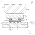
- FIG. 1 is a schematic vertical cross-sectional view showing the configuration of a semiconductor testing apparatus according to Embodiment 1;
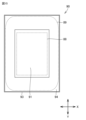
- FIG. 2 is a schematic bottom view showing the configuration of the pressure structure according to Embodiment 1.
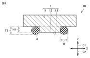
- FIG. 3 is a schematic vertical cross-sectional view taken along line III-III of FIG. 2;
- FIG. 2 is a flow diagram schematically showing a method of testing a semiconductor device according to Embodiment 1; It is a vertical cross-sectional schematic diagram which shows a cooling plate preparation process.
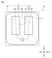
- 1 is a schematic plan view showing the configuration of a semiconductor device;
- FIG. FIG. 7 is a schematic vertical cross-sectional view taken along line VII-VII of FIG. 6; It is a vertical cross-sectional schematic diagram which shows a mounting process.
- FIG. 10 is a schematic vertical cross-sectional view showing a test process using the semiconductor testing apparatus according to the first modified example of the first embodiment;
- FIG. 10 is a schematic vertical cross-sectional view showing a test process using the semiconductor testing apparatus according to the second modification of the first embodiment;
- It is a schematic plan view showing the configuration of a first modification of the semiconductor device.
- It is a schematic plan view showing the configuration of a second modification of the semiconductor device.
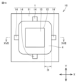
- FIG. 10 is a schematic bottom view showing the configuration of a pressurizing structure according to Embodiment 2;
- FIG. 17 is a schematic vertical cross-sectional view along line XVII-XVII of FIG. 16;
- FIG. 10 is a schematic vertical cross-sectional view showing a test process using the semiconductor testing apparatus according to the second embodiment;
- FIG. 10 is a schematic bottom view showing the configuration of a pressurizing structure according to a modification of Embodiment 2;
- FIG. 20 is a schematic vertical cross-sectional view taken along line XX-XX of FIG. 19;
- FIG. 10 is a schematic vertical cross-sectional view showing a region occupied by a groove according to a modification of the second embodiment;
- FIG. 11 is a schematic vertical cross-sectional view showing a test process using the semiconductor testing apparatus according to Embodiment 3;
- FIG. 11 is a schematic vertical cross-sectional view showing the configuration of an elastic body according to Embodiment 3;
- FIG. 11 is a schematic vertical cross-sectional view showing a configuration of a modification of the elastic body according to Embodiment 3;
- FIG. 4 is a schematic vertical cross-sectional view showing a state in which the pressure applied to the elastic body from the pressure mechanism is released after the electrical characteristics of the semiconductor device are tested in the test process;
- FIG. 11 is a schematic vertical cross-sectional view showing a test process using a semiconductor testing apparatus according to a fourth embodiment;
- FIG. 11 is a schematic bottom view showing the configuration of a pressurizing structure according to Embodiment 5;
- FIG. 28 is a schematic vertical cross-sectional view taken along line XXVIII-XXVIII of FIG. 27;
- FIG. 11 is a schematic plan view showing the configuration of a semiconductor device according to a fifth embodiment;
- FIG. 30 is a schematic vertical cross-sectional view taken along line XXX-XXX in FIG. 29;
- FIG. 12 is a schematic vertical cross-sectional view showing a test process using the semiconductor testing apparatus according to the fifth embodiment;
- FIG. 11 is a schematic bottom view showing the configuration of a pressurizing structure according to a modified example of Embodiment 5;
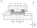
- FIG. 1 is a schematic vertical cross-sectional view showing the configuration of a semiconductor testing apparatus 100 according to Embodiment 1.
- a semiconductor testing apparatus 100 includes a cooling plate 2, a positioning plate 6, a metal foil 3, a pressure plate 1, an elastic body 4, a pressure mechanism 5, and a current supply section 7. , a supply unit 81 , a storage unit 82 , a waste receiving unit 83 , and a transport robot 8 .
- a semiconductor device 90 is placed on the cooling plate 2 .
- the positioning plate 6 positions the semiconductor device 90 .
- Metal foil 3 is placed on semiconductor device 90 .
- a pressure plate 1 is placed on the metal foil 3 .
- the elastic body 4 is attached to the pressure plate 1 .
- the elastic body 4 may be fitted to the pressure plate 1 .
- the elastic body 4 may be fixed to the pressure plate 1 by contracting the elastic body 4 so as to tighten the pressure plate 1 .
- the elastic body 4 may be detachable from the pressure plate 1 .
- Another component may be sandwiched between the elastic body 4 and the pressure plate 1 .
- the elastic body 4 and the pressure plate 1 may be in direct contact with each other.
- the pressure mechanism 5 presses the pressure plate 1 and the elastic body 4 against the semiconductor device 90 .
- the transport robot 8 transports each of the semiconductor device 90 , the metal foil 3 and the pressure plate 1 onto the cooling plate 2 .
- the supply unit 81 supplies members used for testing.
- the storage section 82 stores the semiconductor device 90 for which the test has been completed.
- the disposal receiving section 83 receives members that cannot be reused.
- the cooling plate 2 has a second body portion 21 and a second convex portion 22 .
- the second convex portion 22 continues to the second body portion 21 .
- the second convex portion 22 protrudes from the second body portion 21 toward the semiconductor device 90 .
- the second convex portion 22 protrudes in the first direction 101 from the second main body portion 21 .
- the first direction 101 is the direction from the cooling plate 2 toward the pressure plate 1 .
- the second protrusion 22 forms a mounting surface 23 .
- the semiconductor device 90 is mounted on the cooling plate 2 on the mounting surface 23 .
- the arithmetic average roughness (Ra) of the mounting surface 23 is, for example, 5 ⁇ m or less. Ra of the mounting surface 23 is desirably 2 ⁇ m or less.
- the arithmetic mean roughness (Ra) is a surface texture parameter defined in JIS (Japanese Industrial Standards) B0601:2013.
- the cooling plate 2 has the function of cooling the semiconductor device 90 .
- the cooling plate 2 may have an air cooling mechanism. Specifically, a slit (not shown) may be provided in the second body portion 21 of the cooling plate 2 . Air may be flowed through the slits using a fan or the like (not shown).
- the cooling plate 2 may have a water cooling mechanism. Specifically, a channel may be provided inside the cooling plate 2 . A coolant such as water may be caused to flow through the channel using a circulation device or the like (not shown). If the temperature of the semiconductor device 90 during testing is 80° C. or less, the cooling plate 2 preferably has an air cooling mechanism. If the temperature of the semiconductor device 90 during testing exceeds 80° C., the cooling plate 2 preferably has a liquid cooling mechanism.
- the cooling plate 2 is made of a material with high thermal conductivity and electrical conductivity. Specifically, the cooling plate 2 may be made of metal such as copper or aluminum. Cooling plate 2 may be made of, for example, a carbon material.
- the positioning plate 6 is on the cooling plate 2.
- a through hole 61 is provided in the positioning plate 6 .
- the second protrusion 22 of the cooling plate 2 is inside the through hole 61 .
- the positioning plate 6 has the function of positioning the semiconductor device 90 on the second convex portion 22 of the cooling plate 2 .
- the positioning plate 6 may contact the semiconductor device 90 .
- the semiconductor device 90 is arranged inside the through hole 61 .
- the thickness of the metal foil 3 is set to a first thickness T1.
- the first thickness T1 is, for example, 10 ⁇ m or more and 500 ⁇ m or less.
- the lower limit of the first thickness T1 is not particularly limited, it may be, for example, 50 ⁇ m or more, or 100 ⁇ m or more.
- the upper limit of the first thickness T1 is not particularly limited, it may be, for example, 400 ⁇ m or less, or may be 300 ⁇ m or less.
- the metal foil 3 is made of a metal material that has high electrical conductivity and is as soft as aluminum. Specifically, the metal foil 3 is made of copper, silver, aluminum, or the like, for example.
- the pressure plate 1 is arranged on the semiconductor device 90 .
- a metal foil 3 is between the pressure plate 1 and the semiconductor device 90 .
- the pressure plate 1 has a first body portion 11 , a first convex portion 12 and a pressure surface 13 .
- the first convex portion 12 continues to the first body portion 11 .
- the first convex portion 12 protrudes from the first main body portion 11 toward the semiconductor device 90 .
- the first convex portion 12 protrudes from the first body portion 11 in the second direction 102 .
- a second direction 102 is a direction from the pressure plate 1 toward the cooling plate 2 .
- the first protrusion 12 forms a pressure surface 13 .
- the pressure plate 1 is in contact with the metal foil 3 on the pressure surface 13 .
- Ra of the pressurizing surface 13 is, for example, 5 ⁇ m or less. Ra of the pressurizing surface 13 is desirably 2 ⁇ m or less.
- the cross-section shown in FIG. 1 is a cross-section perpendicular to and through the pressure surface 13 .
- the vertical direction Z is defined as the direction perpendicular to the pressure surface 13 .
- the first direction 101 is parallel to the up-down direction Z.
- the second direction 102 is parallel to the vertical direction Z. As shown in FIG.
- the pressure plate 1 is made of a conductive material. Specifically, pressure plate 1 may be made of a metal material such as aluminum, copper, or stainless steel (SUS). The pressure plate 1 may be made of a carbon material. If the pressure plate 1 is made of copper, it is desirable that the pressure plate 1 is coated with a noble metal. Oxidation of the pressure plate 1 can thereby be suppressed when the pressure plate 1 is made of copper.
- the pressure plate 1 and the elastic body 4 constitute a pressure structure 10.
- the elastic body 4 is attached to the first projection 12 of the pressure plate 1 .
- the elastic body 4 is in contact with the metal foil 3 .
- the elastic body 4 is in contact with the first body portion 11 of the pressure plate 1 .
- the elastic body 4 is sandwiched between the metal foil 3 and the first body portion 11 of the pressure plate 1 .
- the elastic body 4 may be deformed by being sandwiched between the semiconductor device 90 and the first main body 11 .
- the heat resistance temperature of the elastic body 4 is, for example, 250° C. or higher.
- the heat resistance temperature of the elastic body 4 is desirably 300° C. or higher.
- the elastic body 4 is made of, for example, silicone rubber or fluororubber.
- the pressure mechanism 5 is arranged on the pressure plate 1 .
- the pressure mechanism 5 faces the first body portion 11 of the pressure plate 1 .
- the pressurizing mechanism 5 is cylindrical, for example.
- the pressing mechanism 5 extends in the vertical direction Z, for example.
- the pressure mechanism 5, the pressure plate 1, the elastic body 4, the metal foil 3, the semiconductor device 90, the positioning plate 6, and the cooling plate 2 are arranged so that their relative positions in the direction perpendicular to the vertical direction Z do not fluctuate. It may be fixed.
- the pressurizing mechanism 5 can be driven in the vertical direction Z.
- the pressure mechanism 5 has a function of pressing the pressure plate 1 and the elastic body 4 against the semiconductor device 90 via the metal foil 3 .
- a hydraulic jack (not shown) allows the pressure mechanism 5 to apply pressure in the second direction 102 .
- the pressing mechanism 5 is made of a highly rigid and conductive material. Specifically, the pressurizing mechanism 5 is made of, for example, SUS or a carbon material.
- the current supply section 7 is electrically connected to each of the second body section 21 of the cooling plate 2 and the pressure mechanism 5 .
- Each of the second body portion 21 and the pressure mechanism 5 is connected to electrodes of different polarities of the current supply portion 7 .
- the current supply unit 7 can apply current between the cooling plate 2 and the pressure mechanism 5 .
- the current supply unit 7 can apply a direct current between the cooling plate 2 and the pressure mechanism 5, for example.
- the supply unit 81 contains semiconductor devices 90 that have not been tested, unused metal foils 3, and unused pressure structures 10, respectively.
- the waste receiving section 83 stores those metal foils 3, elastic bodies 4, and pressure plates 1 that cannot be reused due to testing.
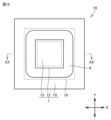
- FIG. 2 is a schematic bottom view showing the configuration of the pressure structure 10 according to Embodiment 1.
- FIG. The schematic bottom view shown in FIG. 2 is a schematic bottom view seen in the up-down direction Z.
- the elastic body 4 surrounds the first projection 12 of the pressure plate 1 when viewed in the vertical direction Z.
- the elastic body 4 surrounds the pressure surface 13 .
- the elastic body 4 is located inside the outer edge of the first body portion 11 of the pressure plate 1 .
- the shape of the elastic body 4 is annular.
- the shape of the pressing surface 13 is, for example, a quadrangle.
- FIG. 3 is a schematic vertical cross-sectional view along line III-III in FIG.
- the schematic cross-sectional view shown in FIG. 3 is a schematic cross-sectional view perpendicular to and passing through the pressure surface 13 .
- elastic body 4 has a circular shape, for example.
- the thickness of the elastic body 4 in the vertical direction Z is the second thickness T2.
- the second thickness T2 is the thickness of the elastic body 4 when it is not deformed.
- the height of the first protrusion 12 of the pressure plate 1 in the vertical direction Z is a first height H1.
- the second thickness T2 is, for example, 1.2 to 1.8 times the first height H1.
- the lower limit of the second thickness T2 is not particularly limited, but may be, for example, 1.3 times or more the first height H1 or 1.4 times or more the first height H1.
- the upper limit of the second thickness T2 is not particularly limited, but may be, for example, 1.7 times or less the first height H1 or 1.6 times or less the first height H1.
- the width of the elastic body 4 in the left-right direction X is the width W.
- the width W is the width of the elastic body 4 when it is not deformed.
- the left-right direction X is a direction parallel to the pressure surface 13 in a cross-sectional view.
- the direction perpendicular to each of the left-right direction X and the up-down direction Z is the front-back direction Y. As shown in FIG.
- FIG. 4 is a flow diagram schematically showing a test method for semiconductor device 90 according to the first embodiment.
- the test method for semiconductor device 90 according to the first embodiment includes a cooling plate preparation step (S10), a mounting step (S20), a pressure mechanism preparation step (S30), a test and a step (S40).
- FIG. 5 is a schematic vertical cross-sectional view showing the cooling plate preparation step (S10).
- the schematic vertical cross-sectional view shown in FIG. 5 is a cross section parallel to the vertical direction Z and passing through the second protrusion 22 of the cooling plate 2 .
- a cold plate 2 is provided.
- a positioning plate 6 is placed on the cooling plate 2 .
- FIG. 6 is a schematic plan view showing the configuration of the semiconductor device 90.
- FIG. 7 is a schematic vertical cross-sectional view taken along line VII--VII in FIG.
- the semiconductor device 90 has a semiconductor substrate 93 , a first electrode 91 , a second electrode 92 , a covering portion 94 and a gate electrode 97 .
- a first electrode 91 is provided on the surface of the semiconductor substrate 93 .
- the first electrode 91 is made of aluminum, for example.
- a second electrode 92 is provided on the back surface of the semiconductor substrate 93 . From another point of view, the second electrode 92 is on the opposite side of the first electrode 91 .
- the second electrode 92 is formed by laminating nickel (Ni) and gold (Au), for example.
- a gate electrode 97 is provided on the surface of the semiconductor substrate 93 .
- the gate electrode 97 is provided on the same surface as the first electrode 91 .
- the gate electrode 97 is on the opposite side of the second electrode 92 . As shown in FIG. 6, gate electrode 97 is spaced apart from first electrode 91 .
- the covering portion 94 partially covers each of the gate electrode 97 and the first electrode 91 .
- the covering portion 94 has a first covering member 95 and a second covering member 96 .
- the outer edge of the first covering member 95 surrounds each of the first electrode 91 and the gate electrode 97 .
- the outer edge of the second covering member 96 surrounds the gate electrode 97 .
- the second covering member 96 continues to the first covering member 95 .
- the first covering member 95 surrounds the second covering member 96 .
- the covering portion 94 covers the outer peripheral portion of the first electrode 91 . From another point of view, part of the covering portion 94 is positioned on the first direction 101 side with respect to the first electrode 91 .
- Covering portion 94 is made of an insulating material such as polyimide, for example.
- the covering portion 94 has a function of suppressing generation of a high electric field.
- the semiconductor device 90 is a MOSFET (Metal Oxide Semiconductor Field Effect Transistor) containing a semiconductor material such as silicon or silicon carbide, which is a wide-gap semiconductor.
- semiconductor substrate 93 is made of silicon or silicon carbide, for example.
- Semiconductor device 90 may be, for example, a Schottky barrier diode or a pn junction diode.
- the semiconductor device 90 has a first pressurized area 88 and a second pressurized area 89 .
- the pressurizing surface 13 (see FIG. 1) of the pressurizing plate 1 is pressed through the metal foil 3 .
- the elastic body 4 (see FIG. 1) is pressed through the metal foil 3 in the second pressurized region 89 .
- the first pressurized region 88 is surrounded by the first covering member 95 of the covering portion 94 .
- the first pressurized region 88 is a region including a portion of each of the first electrode 91 , the gate electrode 97 and the second covering member 96 .
- the first pressurized region 88 When viewed in the vertical direction Z, the first pressurized region 88 is surrounded by the first covering member 95 .
- the area of the first pressurized area 88 is, for example, 0.8 times or more and 1 time or less the area of the area surrounded by the first covering member 95 .
- the second pressurized area 89 continues to the first pressurized area 88 .
- the second pressurized area 89 surrounds the first pressurized area 88 .
- FIG. 8 is a schematic vertical cross-sectional view showing the placing step (S20).
- the vertical cross-sectional schematic diagram shown in FIG. 8 corresponds to the vertical cross-sectional schematic diagram shown in FIG.
- a semiconductor device 90 is mounted on the mounting surface 23 of the cooling plate 2 .
- the transport robot 8 transports the semiconductor device 90 from the supply section 81 onto the mounting surface 23 of the cooling plate 2 .
- the transfer robot 8 places the semiconductor device 90 on the placement surface 23 .
- the area of the mounting surface 23 is, for example, 1 to 1.2 times the area of the semiconductor device 90 viewed from the vertical direction Z.
- the second electrode 92 of the semiconductor device 90 contacts the second protrusion 22 of the cooling plate 2 . Thereby, the second electrode 92 and the cooling plate 2 are electrically connected.
- a metal foil 3 is placed on the semiconductor device 90 .
- the metal foil 3 is arranged on the first electrode 91 and the covering portion 94 .
- the transport robot 8 transports the metal foil 3 from the supply unit 81 onto the placement surface 23 of the cooling plate 2 . Since the semiconductor device 90 is on the mounting surface 23 , the metal foil 3 is mounted on the semiconductor device 90 by the transfer robot 8 . The metal foil 3 is in contact with the covering portion 94 . The metal foil 3 may be spaced apart from the first electrode 91 .
- a pressure structure 10 is placed on the metal foil 3 .
- the conveying robot 8 conveys the pressure structure 10 from the supply unit 81 onto the mounting surface 23 of the cooling plate 2 . Since the metal foil 3 is on the mounting surface 23 , the pressure structure 10 is placed on the metal foil 3 by the transfer robot 8 .
- the elastic body 4 is in contact with the metal foil 3 .
- the pressure plate 1 contacts the metal foil 3 on the pressure surface 13 . Thereby, the pressure plate 1 and the metal foil 3 are electrically connected.
- FIG. 9 is a schematic vertical cross-sectional view showing the pressurizing mechanism preparation step (S30).
- the vertical cross-sectional schematic diagram shown in FIG. 9 corresponds to the vertical cross-sectional schematic diagram shown in FIG.
- the transfer robot 8, supply unit 81, storage unit 82, and waste receiving unit 83 are not shown in FIG.
- the pressure mechanism 5 is arranged on the pressure plate 1 .
- the pressurizing mechanism 5 is arranged so that the central axis of the pressurizing mechanism 5 is parallel to the vertical direction Z.
- the pressure mechanism 5 and the cooling plate 2 are connected to the current supply section 7 .
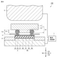
- FIG. 10 is a schematic vertical cross-sectional view showing the test step (S40).
- the vertical cross-sectional schematic diagram shown in FIG. 10 corresponds to the vertical cross-sectional schematic diagram shown in FIG.
- the pressure mechanism 5 drives along the second direction 102 .
- the pressure mechanism 5 is in contact with the first body portion 11 of the pressure plate 1 .
- the pressure structure 10 is pressed against the metal foil 3 by the pressure mechanism 5 .
- the elastic body 4 deforms so as to contract in the vertical direction Z.
- the metal foil 3 is sandwiched between the pressing structure 10 and the semiconductor device 90 .
- the central portion of the metal foil 3 is sandwiched between the pressure surface 13 and the first electrode 91 .
- the outer peripheral portion of the metal foil 3 is sandwiched between the elastic body 4 and the covering portion 94 .
- the pressure mechanism 5 presses the pressure surface 13 against the first electrode 91 via the metal foil 3 .
- the pressing mechanism 5 presses the elastic body 4 against the covering portion 94 via the metal foil 3 .
- the metal foil 3 is deformed so as to conform to the surface shapes of the first electrode 91 and the covering portion 94 of the semiconductor device 90 .
- Metal foil 3 adheres to each of first electrode 91 of semiconductor device 90 and pressure surface 13 of pressure plate 1 .
- the current supply section 7, the pressure mechanism 5, the pressure plate 1, the metal foil 3 and the first electrode 91 are electrically connected to each other.
- Pressure is applied in the second direction 102 by a hydraulic jack (not shown) and the pressure mechanism 5 .
- the lower limit of the applied pressure is not particularly limited, it is desirable to be, for example, 30 kgf/cm 2 or more. That is, although the lower limit of the applied pressure is not particularly limited, it is preferably 2.94 MPa or more. Thereby, the adhesion between each of cooling plate 2 and pressure plate 1 and semiconductor device 90 can be improved.
- the upper limit of the applied pressure is not particularly limited, it is preferably 50 kgf/cm 2 or less, for example. That is, although the upper limit of the applied pressure is not particularly limited, it is preferably 4.9 MPa or less. As a result, it is possible to prevent the load applied to the semiconductor device 90 from becoming excessively large.
- a current is passed between the first electrode 91 and the second electrode 92 of the semiconductor device 90 by the current supply unit 7 . Thereby, the electrical characteristics of the semiconductor device 90 are tested.
- Each of pressing plate 1 , metal foil 3 , semiconductor device 90 and cooling plate 2 generates heat by applying current. Cooling plate 2 cools semiconductor device 90 . As the metal foil 3 generates heat, the metal foil 3 is softened. Thereby, the metal foil 3 is further deformed. Therefore, the metal foil 3 is further adhered to each of the first electrode 91 of the semiconductor device 90 and the pressure plate 1 .
- the pressure mechanism 5 After the current supply is stopped, the pressure mechanism 5 is driven along the first direction 101 . Due to the elastic force, the elastic body 4 is deformed to return to the state before being pressurized.
- the transport robot 8 transports each of the metal foil 3 and the pressure structure 10 that cannot be reused to the waste receiving section 83 (see FIG. 8).
- the transport robot 8 transports the semiconductor device 90 after completion of the test to the storage section 82 (see FIG. 8). As described above, the semiconductor device 90 is tested.
- the pressure mechanism 5 presses only the pressure surface 13 against the semiconductor device 90 via the metal foil 3 .
- the pressure surface 13 is pressed against only one of the covering portion 94 and the first electrode 91 of the semiconductor device 90 .
- the metal foil 3 When the pressure surface 13 is pressed only against the covering portion 94 , the metal foil 3 is sandwiched between the pressure surface 13 and the covering portion 94 . Therefore, the applied pressure concentrates on the covering portion 94 . From another point of view, the pressure applied to the first electrode 91 is reduced. Therefore, the adhesion between the metal foil 3 and the first electrode 91 is lowered. This increases the electrical resistance between the metal foil 3 and the semiconductor device 90 . As a result, it becomes difficult to pass a large current through the semiconductor device 90 during testing.
- the pressure applied by the pressure mechanism 5 is concentrated on a portion of the semiconductor device 90 . Therefore, the adhesion between the second electrode 92 of the semiconductor device 90 and the cooling plate 2 is uneven. As a result, the heat resistance increases in the portion where the adhesion between the second electrode 92 and the cooling plate 2 is low. As a result, the temperature distribution of the second electrode 92 becomes uneven when the semiconductor device 90 is energized.
- FIG. 11 is a schematic bottom view showing the second electrode 92 after the test process in a comparative example that does not have the elastic body 4.
- FIG. 11 a discolored portion 111 is formed on the second electrode 92 due to the uneven temperature distribution of the second electrode 92 .
- the portion of the second electrode 92 outside the first pressurized region 88 is heated to a high temperature, thereby forming the discolored portion 111 .
- a discolored portion 111 is a portion where Ni is deposited on the Au layer in the second electrode 92 .
- the bonding strength of the semiconductor device 90 is lowered at the discolored portion 111 . In other words, the mechanical properties of the semiconductor device 90 deteriorate.
- the pressing mechanism 5 presses the elastic body 4 against the covering portion 94 . Therefore, the elastic body 4 can deform along the surface shape of the covering portion 94 . As a result, it is possible to suppress uneven pressure due to variations in the shape of the covering portion 94 .
- the semiconductor testing apparatus 100 has elastic bodies 4 .
- the elastic body 4 is attached to the pressure plate 1 .
- the pressing mechanism 5 presses the pressing surface 13 against the first electrode 91 via the metal foil 3 .
- the pressing mechanism 5 presses the elastic body 4 against the covering portion 94 via the metal foil 3 . Therefore, the pressure applied by the pressure mechanism 5 is transmitted to the semiconductor device 90 substantially uniformly within the plane. As a result, an increase in electrical resistance between the metal foil 3 and the semiconductor device 90 can be suppressed, and deterioration of the mechanical properties of the semiconductor device 90 can be suppressed.
- the semiconductor testing apparatus 100 has a metal foil 3.
- the metal foil 3 is arranged on the first electrode 91 and the covering portion 94 .
- the pressing mechanism 5 presses the pressing surface 13 against the first electrode 91 via the metal foil 3 .
- the pressing mechanism 5 presses the elastic body 4 against the covering portion 94 via the metal foil 3 . Therefore, the elastic body 4 does not come into direct contact with the semiconductor device 90 .
- the elastic body 4 softens or melts due to heat generated during the test, it is possible to prevent the elastic body 4 from sticking to the semiconductor device 90 . As a result, contamination of the semiconductor device 90 can be suppressed.
- the pressure surface 13 does not come into direct contact with the semiconductor device 90 . As a result, it is possible to prevent the semiconductor device 90 from being scratched due to the contact of the pressure surface 13 .
- the elastic body 4 is attached to the pressure plate 1 . Therefore, the pressure plate 1 and the elastic body 4 can be transported at the same time. Furthermore, relative displacement between the pressure plate 1 and the elastic body 4 can be suppressed. Therefore, the test time of the semiconductor device 90 can be reduced.
- the semiconductor testing apparatus 100 according to Embodiment 1 has a metal foil 3.
- the pressing mechanism 5 presses the pressing surface 13 against the first electrode 91 via the metal foil 3 .
- the metal foil 3 adheres to the first electrode 91 of the semiconductor device 90 and the pressure plate 1 respectively.
- an increase in electrical resistance between the metal foil 3 and the semiconductor device 90 can be further suppressed.
- the semiconductor testing apparatus 100 has a transfer robot 8.
- the transport robot 8 is a mechanism that transports the semiconductor device 90 , the metal foil 3 , and the pressure structure 10 to positions on the cooling plate 2 .
- the work of placing the semiconductor device 90 , the metal foil 3 , and the pressure structure 10 on the cooling plate 2 can be automated.
- the pressure plate 1 has the first convex portion 12 .
- the first convex portion 12 protrudes from the first main body portion 11 toward the semiconductor device 90 .
- the first protrusion 12 forms a pressure surface 13 . Therefore, when the covering portion 94 of the semiconductor device 90 partially covers the first electrode 91 , the pressure surface 13 can be pressed only against the first electrode 91 without pressing the pressure surface 13 against the covering portion 94 . can. This makes it possible to more effectively suppress an increase in electrical resistance between the metal foil 3 and the semiconductor device 90 .
- the second thickness T2 of the elastic body 4 that is not deformed is excessively small, the amount of deformation of the elastic body 4 becomes small when pressure is applied in the test step (S40). Therefore, the pressure applied from the elastic body 4 to the semiconductor device 90 becomes excessively small. This reduces the adhesion between the second electrode 92 of the semiconductor device 90 and the cooling plate 2 .
- the second thickness T2 is 1.2 times or more the height of the first protrusion 12 (first height H1). Therefore, it is possible to prevent the second thickness T2 from becoming excessively small. As a result, deterioration in adhesion between the second electrode 92 of the semiconductor device 90 and the cooling plate 2 can be suppressed.
- the second thickness T2 is 1.8 times or less the height of the first protrusion 12 (first height H1). Therefore, it is possible to prevent the second thickness T2 from becoming excessively large. As a result, it is possible to prevent the elastic body 4 from falling off from the pressure plate 1 .
- the elastic body 4 surrounds the pressure surface 13 when viewed in the vertical direction Z. Therefore, when the covering portion 94 of the semiconductor device 90 covers the outer peripheral portion of the first electrode 91 , the elastic body 4 can be effectively pressed by the covering portion 94 .
- the semiconductor device 90, the metal foil 3, and the pressure plate 1 each generate heat due to the energization in the test step (S40). Therefore, the elastic body 4 is heated in the test process. If the heat resistant temperature of the elastic body 4 is excessively low, the heating of the elastic body 4 may cause the elastic body 4 to melt. If the elastic body 4 is melted, it will stick to the metal foil 3 and the pressure plate 1, so that the elastic body 4 may become unusable after the test process. According to the semiconductor testing apparatus 100 according to the first embodiment, the heat resistance temperature of the elastic body 4 is 250° C. or higher. Therefore, melting of the elastic body 4 in the test step (S40) can be suppressed.
- the metal foil 3 is made of copper, silver, aluminum, or the like. In other words, the metal foil 3 is made of soft metal. Therefore, when the metal foil 3 and the first electrode 91 of the semiconductor device 90 come into contact with each other, the first electrode 91 can be prevented from being scratched.
- the thickness of the metal foil 3 is 10 ⁇ m or more and 500 ⁇ m or less. Therefore, it is possible to prevent the metal foil 3 from tearing as compared with the case where the thickness of the metal foil 3 is excessively thin. Moreover, the metal foil 3 is easily deformed compared to the case where the thickness of the metal foil 3 is excessively thick. Therefore, in the test of the semiconductor device 90 , the adhesion between the pressure plate 1 and the semiconductor device 90 can be further improved by deforming the metal foil 3 .
- Ra of the mounting surface 23 of the cooling plate 2 is, for example, 5 ⁇ m or less. Thereby, the adhesion between the cooling plate 2 and the semiconductor device 90 on the mounting surface 23 can be further improved.
- Ra of the pressing surface 13 of the pressing plate 1 is, for example, 5 ⁇ m or less. As a result, when the pressure surface 13 is pressed against the semiconductor device 90 via the metal foil 3 , it is possible to prevent the pressure surface 13 from damaging the semiconductor device 90 .
- the cooling plate 2 does not have the second protrusions 22
- the heat transmitted from the semiconductor device 90 to the second body portion 21 of the cooling plate 2 is transmitted in the vertical direction Z as well as in the direction perpendicular to the vertical direction Z.
- the temperature in the central portion of the semiconductor device 90 increases and the temperature in the outer peripheral portion of the semiconductor device 90 decreases. In other words, the temperature distribution of the semiconductor device 90 is biased.
- the cooling plate 2 has the second body portion 21 and the second convex portion 22 .
- the second convex portion 22 protrudes from the second body portion 21 toward the semiconductor device 90 .
- the heat transmitted from the semiconductor device 90 to the cooling plate 2 is transmitted to the second main body portion 21 after being transmitted to the second convex portion 22 .
- heat can be prevented from being transmitted in a direction perpendicular to the up-down direction Z.
- bias in the temperature distribution of the semiconductor device 90 can be suppressed.
- the mounting surface 23 of the cooling plate 2 has an excessively small area, part of the second electrode 92 of the semiconductor device 90 does not contact the cooling plate 2 .
- the temperature of the parts of the second electrode 92 that are not in contact with the cooling plate 2 are higher than the temperature of the parts of the second electrode 92 that are in contact with the cooling plate 2 . Therefore, the temperature distribution of the semiconductor device 90 is biased.
- the area of the mounting surface 23 is one or more times the area of the semiconductor device 90 viewed in the vertical direction Z. FIG. Therefore, the entire surface of the second electrode 92 can be in contact with the cooling plate 2 . Thereby, the in-plane uniformity of the temperature distribution of the semiconductor device 90 can be improved.
- the area of the mounting surface 23 of the cooling plate 2 is excessively large, the heat transferred from the semiconductor device 90 to the second convex portion 22 is radiated in a direction parallel to the mounting surface 23 . Therefore, the temperature distribution of the semiconductor device 90 is biased.
- the area of the mounting surface 23 is 1.2 times or less as large as the area of the semiconductor device 90 viewed in the vertical direction Z. FIG. Therefore, it is possible to prevent the area of the mounting surface 23 from becoming excessively large. As a result, bias in the temperature distribution of the semiconductor device 90 can be suppressed.
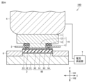
- FIG. 12 is a schematic vertical cross-sectional view showing a test step (S40) using the semiconductor testing apparatus 100 according to the first modification of the first embodiment.
- the vertical cross-sectional schematic diagram shown in FIG. 12 corresponds to the vertical cross-sectional schematic diagram shown in FIG.
- the pressurizing mechanism 5 and the current supply unit 7 are not shown in FIG. 12 .
- semiconductor testing apparatus 100 may have cooling metal foil 9, for example.
- the cooling metal foil 9 is mounted on the mounting surface 23 of the cooling plate 2 .
- the cooling metal foil 9 may cover the mounting surface 23 .
- the cooling metal foil 9 is sandwiched between the second protrusion 22 of the cooling plate 2 and the second electrode 92 of the semiconductor device 90 .
- the thickness of the cooling metal foil 9 is, for example, 10 ⁇ m or more and 500 ⁇ m or less.
- the cooling metal foil 9 is made of a metal material that has high electrical conductivity and is as soft as aluminum. Specifically, the cooling metal foil 9 is made of, for example, copper, silver, or aluminum. When pressure is applied by the pressure mechanism 5, the cooling metal foil 9 is deformed. This allows the cooling metal foil 9 to adhere to each of the second electrode 92 and the cooling plate 2 of the semiconductor device 90 . In other words, the second electrode 92 can adhere to the cooling plate 2 via the cooling metal foil 9 . Therefore, heat generated in the semiconductor device 90 can be more effectively transferred to the cooling plate 2 . Thereby, the semiconductor device 90 can be effectively cooled.
- FIG. 13 is a vertical cross-sectional schematic diagram showing a test process using the semiconductor testing apparatus 100 according to the second modification of the first embodiment.
- the vertical cross-sectional schematic diagram shown in FIG. 13 corresponds to the vertical cross-sectional schematic diagram shown in FIG.
- the metal foil 3 may have a first metal foil 31 and a second metal foil 32 .
- the metal foil 3 may be configured by laminating a plurality of metal foils.
- the number of the plurality of metal foils may be two, or may be three or more.
- a second metal foil 32 is placed on the first metal foil 31 .
- a total value (third thickness T3) of the thickness of the first metal foil 31 and the thickness of the second metal foil 32 is, for example, 10 ⁇ m or more and 500 ⁇ m or less.
- Each of first metal foil 31 and second metal foil 32 is made of, for example, copper, silver, or aluminum.
- the second metal foil 32 can slide on the first metal foil 31 when pressure is applied by the pressure mechanism 5 . Therefore, the amount by which the first metal foil 31 slides on the first electrode 91 can be reduced compared to when the semiconductor testing apparatus 100 does not have the second metal foil 32 . As a result, it is possible to more effectively suppress the occurrence of scratches on the first electrode 91 .
- FIG. 14 is a schematic plan view showing the configuration of the first modified example of the semiconductor device 90.
- semiconductor device 90 may further include current sense electrodes 98 and temperature sense electrodes 99 .
- a current sense electrode 98 is provided on the surface of the semiconductor device. In other words, the current sense electrode 98 is on the opposite side of the second electrode 92 .
- a temperature sensing electrode 99 is provided on the surface of the semiconductor device 90 . In other words, the temperature sense electrode 99 is on the opposite side of the second electrode 92 .
- the semiconductor test apparatus 100 can also test the first modification of the semiconductor device 90 .
- FIG. 15 is a schematic plan view showing the configuration of the second modified example of the semiconductor device 90.
- semiconductor device 90 may not have gate electrode 97 .
- the semiconductor device 90 may be rectangular in shape.
- the semiconductor testing apparatus 100 by changing the shape of each of the elastic body 4 and the pressing surface 13 of the pressing plate 1, the second modification of the semiconductor device 90 can also be tested. can.
- the shape of the pressurizing surface 13 is changed so that the first pressurized region 88 is located inside the first electrode 91 when viewed in the vertical direction Z.
- the shape of the elastic body 4 is changed so that the second pressurized region 89 is positioned inside the semiconductor substrate 93 when viewed in the vertical direction Z.
- Embodiment 2 the configuration of the semiconductor testing apparatus 100 according to the second embodiment will be explained.
- the semiconductor testing apparatus 100 according to the second embodiment differs from the semiconductor testing apparatus 100 according to the first embodiment mainly in that the pressure plate 1 has a supporting portion. is the same as the configuration of the semiconductor testing apparatus 100 according to the first embodiment.
- the following description will focus on the differences from the configuration of the semiconductor testing apparatus 100 according to the first embodiment.
- FIG. 16 is a schematic bottom view showing the configuration of the pressure structure 10 according to Embodiment 2.
- FIG. The schematic bottom view shown in FIG. 16 corresponds to the schematic bottom view shown in FIG. 17 is a schematic vertical cross-sectional view taken along line XVII-XVII in FIG. 16.
- FIG. The vertical cross-sectional schematic diagram shown in FIG. 17 corresponds to the vertical cross-sectional schematic diagram shown in FIG.
- the pressure plate 1 may have a first support portion 14.
- the pressure plate 1 has, for example, four first support portions 14 .
- the first support portion 14 continues to the first body portion 11 .
- the first supporting portion 14 protrudes in the same direction as the first convex portion 12 .
- the first support portion 14 protrudes in the direction from the first body portion 11 toward the first convex portion 12 .
- the first supporting portion 14 is separated from the first convex portion 12 .
- the first supporting portion 14 is outside the first convex portion 12 .
- the elastic body 4 is between the first projection 12 and the first support 14 . From another point of view, the first convex portion 12 and the first support portion 14 support the elastic body 4 by sandwiching it.
- the distance between the first convex portion 12 and the first support portion 14 in the direction parallel to the pressing surface 13 is the distance D.
- the distance D is, for example, 0.9 times or more and 0.95 times or less the width W (see FIG. 3) of the elastic body 4 that is not deformed.
- the elastic body 4 can be sandwiched between the first convex portion 12 and the first support portion 14 .
- the pressure plate 1 has a plurality of first support portions 14, the distance D between each of the plurality of first support portions 14 and the first convex portion 12 may be different.
- the height of the first support portion 14 in the vertical direction Z is the second height H2.
- the second height H2 is smaller than the height of the first projection 12 (first height H1).
- the second height H2 is, for example, 100 ⁇ m smaller than the first height H1.
- FIG. 18 is a schematic vertical cross-sectional view showing the test step (S40) using the semiconductor test apparatus 100 according to the second embodiment.
- the vertical cross-sectional schematic diagram shown in FIG. 18 corresponds to the vertical cross-sectional schematic diagram shown in FIG.
- the first support portion 14 may be spaced apart from the metal foil 3 when pressure is applied by the pressure mechanism 5 (see FIG. 10).
- the pressure plate 1 has the first support portion 14 .
- the first supporting portion 14 is separated from the first convex portion 12 .
- the elastic body 4 is between the first projection 12 and the first support 14 . Therefore, the elastic body 4 is pressed against the semiconductor device 90 via the metal foil 3 while being sandwiched between the first convex portion 12 and the first support portion 14 . As a result, it is possible to suppress displacement of the elastic body 4 in the direction parallel to the pressure surface 13 . As a result, the elastic body 4 can be pressed against the semiconductor device 90 more effectively.
- FIG. 19 is a schematic bottom view showing the configuration of the pressure structure 10 according to the modification of the second embodiment.
- the schematic bottom view shown in FIG. 19 corresponds to the schematic bottom view shown in FIG. 20 is a schematic vertical cross-sectional view taken along line XX-XX in FIG. 19.
- FIG. The vertical cross-sectional schematic diagram shown in FIG. 20 corresponds to the vertical cross-sectional schematic diagram shown in FIG.
- the pressure plate 1 may have a second support portion 15.
- the second support portion 15 continues to the first body portion 11 .
- the second support portion 15 is separated from the first convex portion 12 .
- the second supporting portion 15 surrounds the first convex portion 12 when viewed in the vertical direction Z.
- a groove portion 19 is formed between the first convex portion 12 and the second support portion 15 .
- the width of the groove portion 19 in the direction parallel to the pressure surface 13 decreases as the distance from the first main body portion 11 increases. Therefore, it is possible to prevent the elastic body 4 from falling off from the pressure plate 1 .
- the cross-sectional area of the groove portion 19 is, for example, 0.95 times or more the cross-sectional area of the elastic body 4. As shown in FIG. Therefore, the elastic body 4 can be elastically deformed inside the groove portion 19 .
- the cross-sectional area of the groove portion 19 is the area of the region surrounded by the first body portion 11 , the first convex portion 12 and the second support portion 15 .
- FIG. 21 is a schematic vertical cross-sectional view showing a region occupied by groove portion 19 according to a modification of Embodiment 2. As shown in FIG. The vertical cross-sectional schematic diagram shown in FIG. 21 corresponds to the vertical cross-sectional schematic diagram shown in FIG. For convenience of explanation, the elastic body 4 is not shown in FIG. In FIG. 21 , the areas indicated by a plurality of dots indicate the areas occupied by the grooves 19 .
- the height of the second support portion 15 in the vertical direction Z is the third height H3.
- the third height H3 is smaller than the height of the first protrusion 12 (first height H1).
- the third height H3 is, for example, 100 ⁇ m smaller than the first height H1.
- the semiconductor testing apparatus 100 according to the third embodiment differs from the semiconductor testing apparatus 100 according to the first embodiment mainly in that the cross-sectional shape of the elastic body 4 is polygonal. is the same as the configuration of the semiconductor testing apparatus 100 according to the first embodiment.
- the following description will focus on the differences from the configuration of the semiconductor testing apparatus 100 according to the first embodiment.
- FIG. 22 is a vertical cross-sectional schematic diagram showing a test process using the semiconductor test apparatus 100 according to the third embodiment.
- the vertical cross-sectional schematic diagram shown in FIG. 22 corresponds to the vertical cross-sectional schematic diagram shown in FIG.
- FIG. 23 is an enlarged schematic cross-sectional view showing the configuration of the elastic body 4 according to the third embodiment.
- the cross section shown in FIG. 23 is a cross section parallel to the up-down direction Z.
- the shape of the elastic body 4 may be polygonal.
- the shape of the elastic body 4 may be, for example, a quadrangle.
- the shape of the elastic body 4 may be trapezoidal, for example. Specifically, in a cross section perpendicular to the pressurizing surface 13 , the width of the elastic body 4 may decrease toward the second direction 102 .
- the shape of the elastic body 4 may be square, for example.
- the elastic force in the direction parallel to the cross-section is greater than when the cross-sectional shape of the elastic body 4 is circular. Therefore, by changing the cross-sectional shape of the elastic body 4, the pressure applied from the elastic body 4 to the semiconductor device 90 can be changed.
- FIG. 24 is an enlarged schematic cross-sectional view showing a configuration of a modification of the elastic body 4 according to the third embodiment.
- the enlarged schematic cross-sectional view shown in FIG. 24 corresponds to the enlarged schematic cross-sectional view shown in FIG.
- the elastic body 4 may have a base portion 41 and a projection portion 42 .
- the projecting portion 42 continues to the base portion 41 .
- the protruding portion 42 protrudes from the base portion 41 toward the semiconductor device 90 . In other words, the projecting portion 42 protrudes in the second direction 102 with respect to the base portion 41 .
- the elastic body 4 may have a plurality of protrusions 42 .
- the elastic body 4 can be stably attached to the semiconductor device 90 by determining the shape of the projecting portion 42 of the elastic body 4 so as to match the unevenness of the covering portion 94 . can be pushed.
- Embodiment 4 Next, the configuration of the semiconductor testing apparatus 100 according to Embodiment 4 will be described.
- the semiconductor test apparatus 100 according to the fourth embodiment mainly after the electrical characteristics of the semiconductor device 90 have been tested in the test step (S40), the elastic body 4 is tested before the test. It differs from the configuration of the semiconductor testing apparatus 100 according to the first embodiment in that it restores to substantially the same shape as the shape, and is otherwise the same as the configuration of the semiconductor testing apparatus 100 according to the first embodiment. is.
- the following description will focus on the differences from the configuration of the semiconductor testing apparatus 100 according to the first embodiment.
- FIG. 25 is a schematic vertical cross-sectional view showing a state in which the pressure from the pressure mechanism 5 to the elastic body 4 is released after the electrical characteristics of the semiconductor device 90 are tested in the test step (S40).
- the pressure mechanism 5 is separated from the pressure plate 1 after the electrical characteristics of the semiconductor device 90 are tested.
- the pressure load from the pressure mechanism 5 to the pressure structure 10 is eliminated. From another point of view, the pressure load from the pressing mechanism 5 to the elastic body 4 is eliminated.
- the elastic force of the elastic body 4 may restore the elastic body 4 to substantially the same shape as the elastic body 4 before the test step (S40).
- the thickness (third thickness T3) of the elastic body 4 in the vertical direction Z after the pressure load from the pressurizing mechanism 5 to the elastic body 4 is removed is equal to the thickness of the elastic body 4 in the vertical direction Z before the test. (second thickness T2, see FIG. 3).
- the third thickness T3 is, for example, 95% or more and 100% or less of the second thickness T2.
- the metal foil 3 may be plastically deformed by the pressure load of the pressure structure 10 . After the pressure load from the pressure mechanism 5 to the pressure structure 10 is removed, the metal foil 3 may maintain the shape after being plastically deformed.
- FIG. 26 is a schematic vertical cross-sectional view showing the test step (S40) using the semiconductor test apparatus 100 according to the fourth embodiment.
- the vertical cross-sectional schematic diagram shown in FIG. 26 corresponds to the vertical cross-sectional schematic diagram shown in FIG. FIG. 26 shows the testing step (S40) after the pressure structure 10 has been used in the testing step (S40) at least once.
- pressure is applied to the pressure structure 10 using the pressure mechanism 5 even after the pressure structure 10 has been used in the test step (S40) at least once. By doing so, the elastic body 4 may be deformed so as to shrink in the vertical direction Z.
- the third thickness T3 is 95% or more and 100% or less of the second thickness T2. Therefore, after the test step (S40), it is possible to prevent the thickness of the elastic body 4 from becoming excessively smaller than the height (first height H1) of the first convex portion 12 of the pressure plate 1. FIG. As a result, even when the pressure structure 10 is used repeatedly, the decrease in adhesion between the second electrode 92 of the semiconductor device 90 and the cooling plate 2 can be suppressed.
- the semiconductor testing apparatus 100 even when the elastic body 4 is used repeatedly, the elastic force of the elastic body 4 causes the load from the elastic body 4 to the semiconductor device 90 . A decrease in pressure can be suppressed. Therefore, the pressure structure 10 can be used repeatedly. As a result, the frequency of replacing the pressure structure 10 can be reduced. As a result, the time required for the mounting step (S20) can be reduced, and the stability of the pressure from the elastic body 4 to the semiconductor device 90 can be improved.
- the metal foil 3 maintains the shape after being plastically deformed by the pressure after the pressure load on the pressure structure 10 by the pressure mechanism 5 is removed. ing. Therefore, it is possible to reduce the elastic force with which the metal foil 3 tries to restore the shape of the metal foil 3 before the test after the pressure load on the pressure structure 10 by the pressure mechanism 5 is removed. This can prevent the metal foil 3 from applying pressure to the semiconductor device 90 in an unintended direction. As a result, the pressure applied to the semiconductor device 90 can be accurately controlled.
- Embodiment 5 Next, the configuration of the semiconductor testing apparatus 100 according to Embodiment 5 will be described.
- the semiconductor testing apparatus 100 according to the fifth embodiment differs from the semiconductor testing apparatus 100 according to the first embodiment mainly in that the first convex portion 12 has a plurality of convex members. Other points are the same as the configuration of the semiconductor testing apparatus 100 according to the first embodiment. The following description will focus on the differences from the configuration of the semiconductor testing apparatus 100 according to the first embodiment.
- FIG. 27 is a schematic bottom view showing the configuration of the pressure structure 10 according to Embodiment 5.
- FIG. The schematic bottom view shown in FIG. 27 corresponds to the schematic bottom view shown in FIG. 28 is a schematic vertical cross-sectional view taken along line XXVIII--XXVIII of FIG. 27.
- FIG. The vertical cross-sectional schematic diagram shown in FIG. 28 corresponds to the vertical cross-sectional schematic diagram shown in FIG.
- the first convex portion 12 may have a plurality of convex members. Specifically, the first convex portion 12 has a first convex member 51 and a second convex member 52 .
- the first projecting member 51 continues to the first body portion 11 .
- the first projecting member 51 protrudes in the second direction 102 from the first body portion 11 .
- the second projecting member 52 continues to the first body portion 11 .
- the second projecting member 52 protrudes from the first body portion 11 in the second direction 102 .
- the second projecting member 52 is separated from the first projecting member 51 .
- the height of the first projecting member 51 in the vertical direction Z is the first height H1. In the vertical direction Z, the height of the second projecting member 52 is substantially the same as the first height H1.
- the pressing surface 13 has a first pressing surface portion 71 and a second pressing surface portion 72 .
- the first pressure surface portion 71 is formed by the first projecting member 51 .
- the second pressure surface portion 72 is formed by the second projecting member 52 .
- the second projecting member 52 is separated from the first projecting member 51 .
- the second pressure surface portion 72 and the first pressure surface portion 71 are substantially at the same position. The size and position in the direction parallel to the pressing surface 13 of the first projecting member 51 and the second projecting member 52 are changed so as to match the configuration of the semiconductor device 90 .
- the elastic body 4 there is a portion of the elastic body 4 between the first projecting member 51 and the second projecting member 52 .
- the elastic body 4 is sandwiched between the first projecting member 51 and the second projecting member 52 .
- the elastic body 4 surrounds each of the first projecting member 51 and the second projecting member 52 .
- FIG. 29 is a schematic plan view showing the configuration of a semiconductor device 90 according to the fifth embodiment.
- the schematic plan view shown in FIG. 29 corresponds to the schematic plan view shown in FIG. 30 is a schematic vertical cross-sectional view taken along line XXX-XXX in FIG. 29.
- FIG. The vertical cross-sectional schematic diagram shown in FIG. 30 corresponds to the vertical cross-sectional schematic diagram shown in FIG.
- the first electrode 91 may have a plurality of electrode portions. Specifically, the first electrode 91 may have a first electrode portion 68 and a second electrode portion 69 .
- the number of electrode portions that the first electrode 91 has is the same as the number of convex members that the first convex portion 12 has.
- the first electrode portion 68 and the second electrode portion 69 may be separated from each other by the covering portion 94 . As viewed in the vertical direction Z, each of the first electrode portion 68 and the second electrode portion 69 is surrounded by the covering portion 94 .
- the semiconductor device 90 has a first temperature sense electrode 99A, a second temperature sense electrode 99K, a current sense electrode 98, and a first sense electrode 91S.
- the first temperature sense electrode 99A is the anode.
- the second temperature sense electrode 99K is the cathode.
- Each of the first temperature sense electrode 99A, the second temperature sense electrode 99K, the gate electrode 97, the current sense electrode 98, and the sense electrode 91S of the first electrode is provided on the surface of the semiconductor substrate 93.
- each of the first temperature sense electrode 99A, the second temperature sense electrode 99K, the gate electrode 97, the current sense electrode 98, and the first sense electrode 91S is formed on the same surface as the first electrode 91 is provided. is provided.
- the first electrode 91, the first temperature sense electrode 99A, the second temperature sense electrode 99K, the gate electrode 97, the current sense electrode 98 and the first sense electrode 91S are each separated from each other.
- each of the first temperature sense electrode 99A, the second temperature sense electrode 99K, the gate electrode 97, the current sense electrode 98, and the first sense electrode 91S is surrounded by the covering portion 94. As shown in FIG.
- the first pressurized region 88 has a first portion 86 and a second portion 87. As shown in FIGS. When viewed in the vertical direction Z, the first portion 86 overlaps the first electrode section 68 . At the first portion 86 , the first pressure surface portion 71 is pressed through the metal foil 3 . When viewed in the vertical direction Z, the second portion 87 overlaps the second electrode portion 69 . The second pressure surface portion 72 is pressed against the second portion 87 via the metal foil 3 .
- each of the first portion 86 and the second portion 87 is surrounded by the covering portion 94 .
- the second pressurized region 89 continues to each of the first portion 86 and the second portion 87 .
- a second pressurized region 89 surrounds each of the first portion 86 and the second portion 87 .
- FIG. 31 is a schematic vertical cross-sectional view showing the test step (S40) using the semiconductor test apparatus 100 according to the fifth embodiment.
- the vertical cross-sectional schematic diagram shown in FIG. 31 corresponds to the vertical cross-sectional schematic diagram shown in FIG.
- the first pressure surface portion 71 is pressed against the first electrode portion 68 with the metal foil 3 interposed therebetween.
- the second pressure surface portion 72 is pressed against the second electrode portion 69 with the metal foil 3 interposed therebetween.
- the first convex portion 12 has the first convex member 51 and the second convex member 52 . Therefore, even when the first electrode 91 of the semiconductor device 90 has the first electrode portion 68 and the second electrode portion 69, the first electrode portion 68 and the second electrode portion 69 are substantially can be pressurized simultaneously.
- the semiconductor testing apparatus 100 there is a part of the elastic body 4 between the first projecting member 51 and the second projecting member 52 . Therefore, the elastic body 4 is pressed against the semiconductor device 90 via the metal foil 3 while filling the gap between the first projecting member 51 and the second projecting member 52 . Thereby, the pressurizing mechanism 5 can be electrically connected to each of the first electrode portion 68 and the second electrode portion 69 and can apply a substantially uniform pressure to the semiconductor device 90 . As a result, the in-plane uniformity of the temperature distribution of the semiconductor device 90 can be further improved.
- FIG. 32 is a schematic bottom view showing the configuration of the pressure structure 10 according to the modification of the fifth embodiment.
- the schematic bottom view shown in FIG. 32 corresponds to the schematic bottom view shown in FIG.
- the first projecting member 51 may have a third projecting member 53 .
- the third projecting member 53 is separated from each of the first projecting member 51 and the second projecting member 52 .
- the height of the third projecting member 53 in the vertical direction Z is substantially the same as the first height H1 (see FIG. 28).
- the pressurizing surface 13 may have a third pressurizing surface portion 73 .
- the third pressure surface portion 73 is formed by the third projecting member 53 .
- the third pressure surface portion 73 is separated from each of the first pressure surface portion 71 and the second pressure surface portion 72 .
- the third pressure surface portion 73 is pressed against the gate electrode 97 (see FIG. 29) with the metal foil 3 interposed therebetween.
- the pressing surface 13 has the third pressing surface portion 73 .
- the third pressure surface portion 73 is pressed against the gate electrode 97 via the metal foil 3 . Therefore, the pressure structure 10 can be electrically connected to each of the first electrode portion 68 and the second electrode portion 69 and positively electrically connected to the gate electrode 97 as well. Therefore, the stability of electrical connection between the pressure mechanism 5 and the gate electrode 97 can be improved. Thereby, the potential of the gate electrode 97 can be stabilized. As a result, the stability of the current flowing through the semiconductor device 90 can be improved during testing.
Landscapes
- Physics & Mathematics (AREA)
- General Physics & Mathematics (AREA)
- Testing Of Individual Semiconductor Devices (AREA)
Abstract
半導体デバイス(90)は、第1電極(91)と、第2電極(92)と、被覆部(94)とを有している。第2電極(92)は、第1電極(91)の反対側にある。被覆部(94)は、第1電極(91)の一部を覆う。半導体試験装置(100)は、冷却板(2)と、金属箔(3)と、加圧板(1)と、弾性体(4)と、加圧機構(5)とを有している。冷却板(2)には、半導体デバイス(90)が載置される。金属箔(3)は、第1電極(91)および被覆部(94)の上に配置される。加圧板(1)は、加圧面(13)を有している。加圧板(1)は、金属箔(3)上に載置される。弾性体(4)は、加圧板(1)に装着されている。加圧機構(5)は、金属箔(3)を介して加圧面(13)を第1電極(91)に押しつける。加圧機構(5)は、金属箔(3)を介して弾性体(4)を被覆部(94)に押しつける。
Description
本開示は、半導体試験装置に関するものであり、特にチップ状のパワー半導体デバイスに大電流を通電する通電評価装置に関するものである。
近年、パワー半導体デバイスの大容量化が進んでおり、試験時に通電する電流が増大している。特開2016-11862号公報では、半導体デバイスを加圧しつつ、半導体デバイスに電流を流す半導体試験装置が開示されている。
しかしながら、特許文献1に開示されている半導体試験装置を用いて、被覆部を有している半導体デバイスに対して試験を行う場合、加圧によって生じる応力が被覆部に集中する。このため、半導体試験装置と半導体デバイスの電極との間の密着性が低下する。この結果、半導体試験装置と半導体デバイスの電極との間の電気抵抗が増大する。また、被覆部を避けて加圧した場合、半導体デバイスの一部に応力が集中するため、半導体デバイスと冷却板との間の密着性に偏りが生じる。この結果、半導体デバイスの熱分布に偏りが生じ、半導体デバイスの機械特性が劣化する。
本開示は、上記に鑑みてなされたものであり、その目的は、半導体試験装置と半導体デバイスの電極との間の電気抵抗の増大を抑制可能であり、かつ半導体デバイスの機械特性の劣化を抑制可能な半導体試験装置を提供することである。
本開示に係る半導体試験装置は、半導体デバイスを試験する。半導体デバイスは、第1電極と、第2電極と、被覆部とを含む。第2電極は、第1電極の反対側にある。被覆部は、第1電極の一部を覆う。半導体試験装置は、冷却板と、金属箔と、加圧板と、弾性体と、電流供給部と、加圧機構とを備えている。冷却板は、第2電極と電気的に接続する。冷却板には、半導体デバイスが載置される。金属箔は、第1電極および被覆部の上に配置される。加圧板は、加圧面を含んでいる。加圧板は、金属箔上に載置される。弾性体は、加圧板に装着されている。電流供給部は、冷却板および加圧板の各々と電気的に接続される。電流供給部は、第1電極と第2電極との間に電流を流す。加圧機構は、金属箔を介して加圧面を第1電極に押しつける。加圧機構は、金属箔を介して弾性体を被覆部に押しつける。
本開示に係る半導体試験装置によれば、加圧面が半導体デバイスの第1電極に押しつけられ、かつ弾性体が半導体デバイスの被覆部に押しつけられる。この結果、半導体デバイスと半導体試験装置の間の電気抵抗の増大を抑制することができ、かつ半導体デバイスの機械特性の劣化を抑制することができる。
以下、図面に基づいて本開示の実施の形態について説明する。なお、以下の図面において同一または相当する部分には同一の参照番号を付し、その説明は繰返さない。
実施の形態1.
実施の形態1に係る半導体試験装置の構成について説明する。図1は、実施の形態1に係る半導体試験装置100の構成を示す縦断面模式図である。図1に示されるように、半導体試験装置100は、冷却板2と、位置決め板6と、金属箔3と、加圧板1と、弾性体4と、加圧機構5と、電流供給部7と、供給部81と、収納部82と、廃棄受入部83と、搬送ロボット8とを主に有している。
実施の形態1に係る半導体試験装置の構成について説明する。図1は、実施の形態1に係る半導体試験装置100の構成を示す縦断面模式図である。図1に示されるように、半導体試験装置100は、冷却板2と、位置決め板6と、金属箔3と、加圧板1と、弾性体4と、加圧機構5と、電流供給部7と、供給部81と、収納部82と、廃棄受入部83と、搬送ロボット8とを主に有している。
冷却板2には、半導体デバイス90が載置される。位置決め板6は、半導体デバイス90を位置決めする。金属箔3は、半導体デバイス90上に配置される。加圧板1は、金属箔3上に載置される。弾性体4は、加圧板1に装着されている。具体的には、弾性体4は、加圧板1に嵌め合わされていてもよい。加圧板1を締め付けるように弾性体4が収縮することによって、弾性体4は加圧板1に固定されていてもよい。弾性体4は、加圧板1に対して着脱可能であってもよい。弾性体4と加圧板1との間において、他の部品が挟まれていてもよい。弾性体4と加圧板1とは、直接接していてもよい。
加圧機構5は、加圧板1および弾性体4を半導体デバイス90に押しつける。搬送ロボット8は、半導体デバイス90、金属箔3および加圧板1の各々を冷却板2上へ搬送する。供給部81は、試験に使用される部材を供給する。収納部82は、試験が完了した半導体デバイス90を収納する。廃棄受入部83は、再使用不可となった部材を受け入れる。
冷却板2は、第2本体部21と、第2凸部22とを有している。第2凸部22は、第2本体部21に連なっている。第2凸部22は、第2本体部21から半導体デバイス90側に突出している。言い換えれば、第2凸部22は、第2本体部21から第1方向101に突出している。なお、第1方向101は、冷却板2から加圧板1に向かう方向である。第2凸部22は、載置面23を形成している。載置面23において、半導体デバイス90は冷却板2に載置される。載置面23の算術平均粗さ(Ra)は、たとえば5μm以下である。載置面23のRaは、望ましくは2μm以下である。なお、算術平均粗さ(Ra)は、JIS(Japanese Industrial Standards) B0601:2013に規定される表面性状パラメータである。
冷却板2は、半導体デバイス90を冷却する機能を有している。冷却板2は、空冷機構を有していてもよい。具体的には、冷却板2の第2本体部21において、非図示のスリットが設けられていてもよい。非図示のファン等を用いて、スリットに空気が流されてもよい。冷却板2は、水冷機構を有していてもよい。具体的には、冷却板2の内部において、流路が設けられていてもよい。非図示の循環装置等を用いて、流路に水等の冷媒が流されてもよい。試験時における半導体デバイス90の温度が80℃以下である場合においては、冷却板2は空冷機構を有していることが望ましい。試験時における半導体デバイス90の温度が80℃を超える場合においては、冷却板2は液冷機構を有していることが望ましい。
冷却板2は、熱伝導率が高く、かつ導電性を有している材質によって構成されている。具体的には、冷却板2は、たとえば銅またはアルミニウム等の金属によって構成されていてもよい。冷却板2は、たとえば炭素材料によって構成されていてもよい。
図1に示されるように、位置決め板6は冷却板2上にある。位置決め板6において、貫通孔61が設けられている。冷却板2の第2凸部22は、貫通孔61の内側にある。位置決め板6は、半導体デバイス90を冷却板2の第2凸部22上に位置決めする機能を有している。位置決め板6は、半導体デバイス90に接してもよい。半導体デバイス90は、貫通孔61の内側に配置される。
図1に示されるように、金属箔3は、半導体デバイス90に接する。金属箔3の厚みは、第1厚みT1とされる。第1厚みT1は、たとえば10μm以上500μm以下である。第1厚みT1の下限は、特に限定されないが、たとえば50μm以上であってもよいし、100μm以上であってもよい。第1厚みT1の上限は、特に限定されないが、たとえば400μm以下であってもよいし、300μm以下であってもよい。金属箔3は、電気伝導度が高く、かつアルミニウムと同程度の柔らかさを有する金属材料によって構成されている。具体的には、金属箔3は、たとえば銅、銀またはアルミニウム等によって構成されている。
図1に示されるように、加圧板1は、半導体デバイス90上に配置される。金属箔3は、加圧板1と半導体デバイス90との間にある。加圧板1は、第1本体部11と、第1凸部12と、加圧面13とを有している。第1凸部12は、第1本体部11に連なっている。第1凸部12は、第1本体部11から半導体デバイス90側に突出している。言い換えれば、第1凸部12は、第1本体部11から第2方向102に突出している。なお、第2方向102は、加圧板1から冷却板2に向かう方向である。第1凸部12は、加圧面13を形成している。加圧面13において、加圧板1は金属箔3に接している。加圧面13のRaは、たとえば5μm以下である。加圧面13のRaは、望ましくは2μm以下である。図1に示される断面は、加圧面13に垂直であり、かつ加圧面13を通る断面である。本明細書において、加圧面13に垂直な方向は上下方向Zとされる。第1方向101は、上下方向Zに平行である。第2方向102は、上下方向Zに平行である。
加圧板1は、導電性を有する材料によって構成されている。具体的には、加圧板1は、たとえばアルミニウム、銅またはステンレス鋼(SUS)等の金属材料によって構成されていてもよい。加圧板1は、炭素材料によって構成されていてもよい。加圧板1が銅によって構成されている場合、加圧板1は貴金属でコーティングされていることが望ましい。これによって、加圧板1が銅である場合において、加圧板1の酸化を抑制することができる。
図1に示されるように、加圧板1と弾性体4とは、加圧構造体10を構成している。弾性体4は、加圧板1の第1凸部12に装着されている。弾性体4は、金属箔3に接している。弾性体4は、加圧板1の第1本体部11に接している。言い換えれば、弾性体4は、金属箔3と加圧板1の第1本体部11との間に挟まれている。図1に示されるように、弾性体4は、半導体デバイス90と第1本体部11との間に挟まれることにより変形していてもよい。弾性体4の耐熱温度は、たとえば250℃以上である。弾性体4の耐熱温度は、望ましくは300℃以上である。弾性体4は、たとえばシリコーンゴムまたはフッ素ゴム等により構成されている。
加圧機構5は、加圧板1上に配置される。加圧機構5は、加圧板1の第1本体部11に対向している。加圧機構5は、たとえば円柱状である。加圧機構5は、たとえば上下方向Zに延びている。加圧機構5、加圧板1、弾性体4、金属箔3、半導体デバイス90、位置決め板6および冷却板2の各々は、上下方向Zに垂直な方向における互いの相対位置が変動しないように、固定されていてもよい。
加圧機構5は上下方向Zに駆動可能である。加圧機構5は、加圧板1および弾性体4の各々を、金属箔3を介して半導体デバイス90に押しつける機能を有している。非図示の油圧ジャッキにより、加圧機構5は、第2方向102に圧力を負荷できる。加圧機構5は、剛性が高く、かつ導電性を有している材料によって構成されている。具体的には、加圧機構5は、たとえばSUSまたは炭素材料等によって構成されている。
電流供給部7は、冷却板2の第2本体部21および加圧機構5の各々に電気的に接続されている。第2本体部21および加圧機構5の各々は、互いに電流供給部7の異なる極性の電極に接続されている。電流供給部7は、冷却板2と加圧機構5との間に電流を流すことができる。具体的には、電流供給部7は、たとえば冷却板2と加圧機構5との間に直流電流を流すことができる。
供給部81は、試験が実施されていない半導体デバイス90、未使用の金属箔3、未使用の加圧構造体10の各々を収納している。廃棄受入部83は、金属箔3、弾性体4および加圧板1の各々の内、試験によって再使用不可となったものを収納している。
図2は、実施の形態1に係る加圧構造体10の構成を示す底面模式図である。図2に示される底面模式図は、上下方向Zに見た底面模式図である。図2に示されるように、上下方向Zに見て、弾性体4は、加圧板1の第1凸部12を取り囲んでいる。上下方向Zに見て、弾性体4は、加圧面13を取り囲んでいる。上下方向Zに見て、弾性体4は、加圧板1の第1本体部11の外縁よりも内側にある。上下方向Zに見て、弾性体4の形状は環状である。上下方向Zに見て、加圧面13の形状は、たとえば四角形である。
図3は、図2のIII-III線に沿う縦断面模式図である。図3に示される断面模式図は、加圧面13に垂直であり、かつ加圧面13を通る断面模式図である。図3に示されるように、加圧面13に垂直な断面(以下、断面視とも称する)において、弾性体4の形状はたとえば円形である。
図3に示されるように、上下方向Zにおける弾性体4の厚みは、第2厚みT2とされる。なお、第2厚みT2は、変形していない状態における弾性体4の厚みである。図3に示されるように、上下方向Zにおける加圧板1の第1凸部12の高さは、第1高さH1とされる。第2厚みT2は、たとえば第1高さH1の1.2倍以上1.8倍以下である。第2厚みT2の下限は、特に限定されないが、たとえば第1高さH1の1.3倍以上であってもよいし、第1高さH1の1.4倍以上であってもよい。第2厚みT2の上限は、特に限定されないが、たとえば第1高さH1の1.7倍以下であってもよいし、第1高さH1の1.6倍以下であってもよい。左右方向Xにおける弾性体4の幅は、幅Wとされる。なお、幅Wは、変形していない状態における弾性体4の幅である。なお、本明細書において左右方向Xとは、断面視における加圧面13に平行な方向である。図2に示されるように、左右方向Xおよび上下方向Zの各々に垂直な方向は、前後方向Yとされる。
(半導体デバイスの試験方法)
次に、実施の形態1に係る半導体デバイス90の試験方法について説明する。図4は、実施の形態1に係る半導体デバイス90の試験方法を概略的に示すフロー図である。図4に示されるように、実施の形態1に係る半導体デバイス90の試験方法は、冷却板準備工程(S10)と、載置工程(S20)と、加圧機構準備工程(S30)と、試験工程(S40)とを有している。
次に、実施の形態1に係る半導体デバイス90の試験方法について説明する。図4は、実施の形態1に係る半導体デバイス90の試験方法を概略的に示すフロー図である。図4に示されるように、実施の形態1に係る半導体デバイス90の試験方法は、冷却板準備工程(S10)と、載置工程(S20)と、加圧機構準備工程(S30)と、試験工程(S40)とを有している。
まず、冷却板準備工程(S10)が実施される。図5は、冷却板準備工程(S10)を示す縦断面模式図である。図5に示される縦断面模式図は、上下方向Zに平行であり、かつ冷却板2の第2凸部22を通る断面である。図5に示されるように、冷却板2が準備される。冷却板2上に、位置決め板6が載置される。
次に、半導体デバイス90の構成について説明する。図6は、半導体デバイス90の構成を示す平面模式図である。図7は、図6のVII-VII線に沿う縦断面模式図である。図6および図7に示されるように、半導体デバイス90は、半導体基板93と、第1電極91と、第2電極92と、被覆部94と、ゲート電極97とを有している。
半導体基板93の表面において、第1電極91は設けられている。第1電極91は、たとえばアルミニウムによって構成されている。半導体基板93の裏面において、第2電極92は設けられている。別の観点から言えば、第2電極92は、第1電極91の反対側にある。第2電極92は、たとえばニッケル(Ni)と金(Au)とが積層されることにより形成されている。
半導体基板93の表面において、ゲート電極97は設けられている。言い換えれば、第1電極91と同じ面において、ゲート電極97は設けられている。別の観点から言えば、ゲート電極97は、第2電極92の反対側にある。図6に示されるように、ゲート電極97は、第1電極91から離間している。
被覆部94は、ゲート電極97および第1電極91の各々の一部を覆っている。被覆部94は、第1被覆部材95と、第2被覆部材96とを有している。上下方向Zに見て、第1被覆部材95の外縁は、第1電極91およびゲート電極97の各々を取り囲んでいる。上下方向Zに見て、第2被覆部材96の外縁は、ゲート電極97を取り囲んでいる。第2被覆部材96は、第1被覆部材95に連なっている。上下方向Zに見て、第1被覆部材95は、第2被覆部材96を取り囲んでいる。
図6および図7に示されるように、被覆部94は、第1電極91の外周部を覆っている。別の観点から言えば、被覆部94の一部は、第1電極91に対して第1方向101側に位置している。被覆部94は、たとえばポリイミド等の絶縁性材料によって構成されている。被覆部94は、高電界の発生を抑制する機能を有している。半導体デバイス90は、たとえばシリコンまたはワイドギャップ半導体であるシリコンカーバイドなどの半導体材料を含むMOSFET(Metal Oxide Semiconductor Field Effect Transistor)である。具体的には、半導体基板93は、たとえばシリコンまたはシリコンカーバイドによって構成されている。半導体デバイス90は、たとえばショットキーバリアダイオードまたはpn接合ダイオードであってもよい。
図6および図7に示されるように、半導体デバイス90は、第1被加圧領域88と、第2被加圧領域89とを有している。第1被加圧領域88において、金属箔3を介して加圧板1の加圧面13(図1参照)が押しつけられる。第2被加圧領域89において、金属箔3を介して弾性体4(図1参照)が押しつけられる。上下方向Zに見て、第1被加圧領域88は、被覆部94の第1被覆部材95に取り囲まれている。上下方向Zに見て、第1被加圧領域88は、第1電極91、ゲート電極97および第2被覆部材96の各々の一部を含む領域である。上下方向Zに見て、第1被加圧領域88は、第1被覆部材95に取り囲まれている。上下方向Zに見て、第1被加圧領域88の面積は、たとえば第1被覆部材95に囲まれる領域の面積の0.8倍以上1倍以下である。第2被加圧領域89は、第1被加圧領域88に連なっている。第2被加圧領域89は、第1被加圧領域88を取り囲んでいる。
次に、載置工程(S20)が実施される。図8は、載置工程(S20)を示す縦断面模式図である。図8に示される縦断面模式図は、図5に示される縦断面模式図に対応している。図8に示されるように、冷却板2の載置面23上に、半導体デバイス90が載置される。具体的には、搬送ロボット8によって、半導体デバイス90が供給部81から冷却板2の載置面23上に搬送される。その後、搬送ロボット8によって、半導体デバイス90が載置面23上に載置される。載置面23の面積は、たとえば上下方向Zから見た半導体デバイス90の面積の1倍以上1.2倍以下である。載置面23において、半導体デバイス90の第2電極92は、冷却板2の第2凸部22に接する。これによって、第2電極92と冷却板2とは、電気的に接続される。
半導体デバイス90上に金属箔3が載置される。言い換えれば、金属箔3は、第1電極91および被覆部94の上に配置される。具体的には、搬送ロボット8によって、金属箔3が供給部81から冷却板2の載置面23上に搬送される。載置面23上に半導体デバイス90があるため、搬送ロボット8によって、金属箔3は半導体デバイス90上に載置される。金属箔3は、被覆部94に接する。金属箔3は、第1電極91から離間していてもよい。
金属箔3上に加圧構造体10が載置される。具体的には、搬送ロボット8によって、供給部81から冷却板2の載置面23上へ加圧構造体10が搬送される。載置面23上に金属箔3があるため、搬送ロボット8によって、加圧構造体10は、金属箔3上に載置される。弾性体4は、金属箔3に接する。加圧面13において、加圧板1は、金属箔3に接する。これによって、加圧板1と金属箔3とは、電気的に接続される。
次に、加圧機構準備工程(S30)が実施される。図9は、加圧機構準備工程(S30)を示す縦断面模式図である。図9に示される縦断面模式図は、図5に示される縦断面模式図に対応している。なお、説明の便宜のため、図9において、搬送ロボット8、供給部81、収納部82および廃棄受入部83の各々は図示されていない。図9に示されるように、加圧機構5は、加圧板1上に配置される。加圧機構5の中心軸が上下方向Zに平行となるように、加圧機構5は配置される。加圧機構5と、冷却板2とは、電流供給部7に接続される。
次に、試験工程(S40)が実施される。図10は、試験工程(S40)を示す縦断面模式図である。図10に示される縦断面模式図は、図9に示される縦断面模式図に対応している。加圧機構5が第2方向102に沿って駆動する。
加圧機構5は、加圧板1の第1本体部11に接する。加圧機構5によって、加圧構造体10が金属箔3に押しつけられる。弾性体4は、上下方向Zに縮むように変形する。金属箔3は、加圧構造体10と半導体デバイス90との間に挟み込まれる。具体的には、金属箔3の中央部は加圧面13と第1電極91とによって挟み込まれる。金属箔3の外周部は弾性体4と被覆部94とによって挟み込まれる。別の観点から言えば、加圧機構5は、金属箔3を介して加圧面13を第1電極91に押しつける。加圧機構5は、金属箔3を介して弾性体4を被覆部94に押しつける。これによって、金属箔3は、半導体デバイス90の第1電極91および被覆部94の表面形状に沿うように変形する。金属箔3は、半導体デバイス90の第1電極91および加圧板1の加圧面13の各々に密着する。これによって、電流供給部7、加圧機構5、加圧板1、金属箔3および第1電極91の各々は、互いに電気的に接続される。
非図示の油圧ジャッキおよび加圧機構5によって、第2方向102に圧力が負荷される。負荷される圧力の下限は、特に制限されないが、たとえば30kgf/cm2以上であることが望ましい。すなわち、負荷される圧力の下限は、特に制限されないが、2.94MPa以上であることが望ましい。これによって、冷却板2および加圧板1の各々と半導体デバイス90との密着性を向上することができる。
負荷される圧力の上限は、特に制限されないが、たとえば50kgf/cm2以下であることが望ましい。すなわち、負荷される圧力の上限は、特に制限されないが、4.9MPa以下であることが望ましい。これによって、半導体デバイス90に加わる負荷が過剰に大きくなることを抑制できる。
電流供給部7によって半導体デバイス90の第1電極91と第2電極92との間に電流が流される。これによって、半導体デバイス90の電気的特性が試験される。電流が流されることによって、加圧板1、金属箔3、半導体デバイス90および冷却板2の各々は発熱する。冷却板2は、半導体デバイス90を冷却する。金属箔3が発熱することにより、金属箔3は軟化する。これによって、金属箔3はさらに変形する。このため、金属箔3は、半導体デバイス90の第1電極91および加圧板1の各々にさらに密着する。
電流の供給が停止された後、加圧機構5は、第1方向101に沿って駆動する。弾性力によって、弾性体4は加圧される前の状態に戻るように変形する。搬送ロボット8によって、再使用不可となった金属箔3および加圧構造体10の各々は、廃棄受入部83(図8参照)へ搬送される。搬送ロボット8によって、試験完了後の半導体デバイス90は、収納部82(図8参照)へ搬送される。以上のように、半導体デバイス90の試験が実施される。
次に、実施の形態1に係る半導体試験装置100の作用効果について説明する。
半導体試験装置100が弾性体4を有していない場合、加圧機構5は、金属箔3を介して加圧面13のみを半導体デバイス90に押しつける。この場合、半導体デバイス90の被覆部94および第1電極91のいずれか一方のみに、加圧面13は押しつけられる。
半導体試験装置100が弾性体4を有していない場合、加圧機構5は、金属箔3を介して加圧面13のみを半導体デバイス90に押しつける。この場合、半導体デバイス90の被覆部94および第1電極91のいずれか一方のみに、加圧面13は押しつけられる。
加圧面13が被覆部94にのみ押しつけられる場合、金属箔3は加圧面13と被覆部94との間に挟み込まれる。このため、負荷される圧力は、被覆部94に集中する。別の観点から言えば、第1電極91に負荷される圧力は小さくなる。このため、金属箔3と第1電極91との間の密着性が低下する。これによって、金属箔3と半導体デバイス90との間の電気抵抗が増大する。この結果、試験において、半導体デバイス90に大きな電流を流すことが困難になる。
加圧面13が第1電極91にのみ押しつけられる場合、加圧機構5によって負荷される圧力は、半導体デバイス90の一部に集中する。このため、半導体デバイス90の第2電極92と冷却板2との間の密着性に偏りが生じる。これによって、第2電極92と冷却板2との間の密着性が低い部分において、熱抵抗が高くなる。この結果、半導体デバイス90に通電した際に、第2電極92の温度分布に偏りが生じる。
図11は、弾性体4を有していない比較例における試験工程後の第2電極92を示す底面模式図である。図11に示されるように、第2電極92の温度分布に偏りが生じることによって、第2電極92に変色部111が形成される。具体的には、第1被加圧領域88の外側にある第2電極92の部分が高温になることによって、変色部111が形成される。変色部111は、第2電極92中のAu層にNiが析出した部分である。半導体デバイス90がプリント基板等に実装される場合、変色部111において半導体デバイス90の接合強度が低下する。言い換えれば、半導体デバイス90の機械特性が劣化する。
実施の形態1に係る半導体試験装置100によれば、加圧機構5は、弾性体4を被覆部94に押しつける。このため、弾性体4は、被覆部94の表面形状に沿うように変形することができる。これによって、被覆部94の形状のばらつきによる圧力の偏りを抑制することができる。
実施の形態1に係る半導体試験装置100は、弾性体4を有している。弾性体4は、加圧板1に装着されている。加圧機構5は、金属箔3を介して加圧面13を第1電極91に押しつける。加圧機構5は、金属箔3を介して弾性体4を被覆部94に押しつける。このため、加圧機構5によって負荷される圧力は、半導体デバイス90に対して実質的に面内均一に伝わる。これによって、金属箔3と半導体デバイス90との間の電気抵抗の増大を抑制することができ、かつ半導体デバイス90の機械特性の劣化を抑制することができる。
実施の形態1に係る半導体試験装置100は、金属箔3を有している。金属箔3は、第1電極91および被覆部94の上に配置される。加圧機構5は、金属箔3を介して加圧面13を第1電極91に押しつける。加圧機構5は、金属箔3を介して弾性体4を被覆部94に押しつける。このため、弾性体4は、半導体デバイス90に直接接触しない。これによって、弾性体4に付着した異物または弾性体4の発塵により発生した異物が、半導体デバイス90に付着することを抑制できる。また、試験時の発熱により、弾性体4が軟化または溶融した場合において、弾性体4が半導体デバイス90に固着することを抑制できる。この結果、半導体デバイス90の汚染を抑制できる。
また、加圧面13は、半導体デバイス90に直接接触しない。これによって、加圧面13の接触による半導体デバイス90の傷の発生を抑制することができる。
実施の形態1に係る半導体試験装置100によれば、弾性体4は加圧板1に装着されている。このため、加圧板1と弾性体4とを同時に搬送することができる。さらに、加圧板1と弾性体4との間における相対的な位置ずれを抑制できる。このため、半導体デバイス90の試験時間を低減することができる。
実施の形態1に係る半導体試験装置100は、金属箔3を有している。加圧機構5は、金属箔3を介して加圧面13を第1電極91に押しつける。これによって、圧力が負荷された際に、金属箔3は、半導体デバイス90の第1電極91および加圧板1の各々に密着する。この結果、金属箔3と半導体デバイス90との間の電気抵抗の増大をさらに抑制することができる。
実施の形態1に係る半導体試験装置100は、搬送ロボット8を有している。搬送ロボット8は、半導体デバイス90、金属箔3、加圧構造体10の各々を冷却板2上の位置に搬送する機構である。これによって、半導体デバイス90、金属箔3、加圧構造体10の各々を冷却板2に載置する作業を自動化することができる。
実施の形態1に係る半導体試験装置100によれば、加圧板1は、第1凸部12を有している。第1凸部12は、第1本体部11から半導体デバイス90側に突出している。第1凸部12は、加圧面13を形成している。このため、半導体デバイス90の被覆部94が第1電極91の一部を覆っている場合において、加圧面13を被覆部94に押しつけることなく、加圧面13を第1電極91のみに押しつけることができる。これによって、金属箔3と半導体デバイス90との間の電気抵抗の増大をより効果的に抑制することができる。
変形していない弾性体4の厚み(第2厚みT2)が過度に小さい場合、試験工程(S40)において圧力が負荷された際に、弾性体4の変形量が小さくなる。このため、弾性体4から半導体デバイス90に加わる圧力が過度に小さくなる。これによって、半導体デバイス90の第2電極92と冷却板2との密着性が低下する。実施の形態1に係る半導体試験装置100によれば、第2厚みT2は、第1凸部12の高さ(第1高さH1)の1.2倍以上である。このため、第2厚みT2が過度に小さくなることを抑制できる。この結果、半導体デバイス90の第2電極92と冷却板2との密着性の低下を抑制できる。
変形していない弾性体4の厚み(第2厚みT2)が過度に大きい場合、弾性体4の自重によって弾性体4が加圧板1から脱落するおそれがある。実施の形態1に係る半導体試験装置100によれば、第2厚みT2は、第1凸部12の高さ(第1高さH1)の1.8倍以下である。このため、第2厚みT2が過度に大きくなることを抑制できる。この結果、弾性体4の加圧板1からの脱落を抑制できる。
実施の形態1に係る半導体試験装置100によれば、上下方向Zに見て、弾性体4は、加圧面13を取り囲んでいる。このため、半導体デバイス90の被覆部94が第1電極91の外周部を覆っている場合において、弾性体4を被覆部94により効果的に押しつけることができる。
試験工程(S40)における通電によって半導体デバイス90、金属箔3および加圧板1の各々は発熱する。このため、試験工程において、弾性体4は加熱される。弾性体4の耐熱温度が過度に低い場合、弾性体4の加熱によって、弾性体4が溶融するおそれがある。弾性体4が溶融した場合、弾性体4が金属箔3および加圧板1の各々に固着するため、試験工程後に弾性体4は再使用不可能になるおそれがある。実施の形態1に係る半導体試験装置100によれば、弾性体4の耐熱温度は、250℃以上である。このため、試験工程(S40)における弾性体4の溶融を抑制することができる。
実施の形態1に係る半導体試験装置100によれば、金属箔3は、銅、銀またはアルミニウム等によって構成されている。言い換えれば、金属箔3は、柔らかい金属によって構成されている。このため、金属箔3と半導体デバイス90の第1電極91とが接触した際に、第1電極91における傷の発生を抑制することができる。
実施の形態1に係る半導体試験装置100によれば、金属箔3の厚みは、10μm以上500μm以下である。このため、金属箔3の厚みが過度に薄い場合と比較して、金属箔3が破れることを抑制できる。また、金属箔3の厚みが過度に厚い場合と比較して、金属箔3は容易に変形する。従って、半導体デバイス90の試験において、金属箔3が変形することにより、加圧板1と半導体デバイス90の間の密着性をより向上することができる。
実施の形態1に係る半導体試験装置100によれば、冷却板2の載置面23のRaは、たとえば5μm以下である。これによって、載置面23における冷却板2と半導体デバイス90との密着性をより向上することができる。
実施の形態1に係る半導体試験装置100によれば、加圧板1の加圧面13のRaは、たとえば5μm以下である。これによって、金属箔3を介して加圧面13が半導体デバイス90に押しつけられる際に、加圧面13が半導体デバイス90を傷つけること抑制できる。
冷却板2が第2凸部22を有していない場合、半導体デバイス90から冷却板2の第2本体部21に伝わった熱は、上下方向Zとともに上下方向Zに垂直な方向にも伝わる。このため、半導体デバイス90の中央部の温度が高くなり、半導体デバイス90の外周部の温度は低くなる。言い換えれば、半導体デバイス90の温度分布の偏りが生じる。実施の形態1に係る半導体試験装置100によれば、冷却板2は、第2本体部21と、第2凸部22を有している。第2凸部22は、第2本体部21から半導体デバイス90側に突出している。このため、半導体デバイス90から冷却板2に伝わった熱は、第2凸部22に伝わった後に、第2本体部21に伝わる。これによって、熱が上下方向Zに垂直な方向に伝わることを抑制できる。この結果、半導体デバイス90の温度分布の偏りを抑制できる。
冷却板2の載置面23の面積が過度に小さい場合、半導体デバイス90の第2電極92の一部は、冷却板2に接しない。試験において、冷却板2に接していない第2電極92の部分の温度は、冷却板2に接している第2電極92の部分の温度と比較して高くなる。このため、半導体デバイス90の温度分布の偏りが生じる。実施の形態1に係る半導体試験装置100によれば、載置面23の面積は、上下方向Zに見た半導体デバイス90の面積の1倍以上である。このため、第2電極92の全面が冷却板2に接することができる。これによって、半導体デバイス90の温度分布の面内均一性を向上することができる。
冷却板2の載置面23の面積が過度に大きい場合、半導体デバイス90から第2凸部22に伝わった熱は、載置面23に平行な方向に放熱される。このため、半導体デバイス90の温度分布の偏りが生じる。実施の形態1に係る半導体試験装置100によれば、載置面23の面積は、上下方向Zに見た半導体デバイス90の面積の1.2倍以下である。このため、載置面23の面積が過度に大きくなることを抑制できる。これによって、半導体デバイス90の温度分布の偏りを抑制できる。
(実施の形態1の変形例)
半導体試験装置100の構成は、上記の構成に限定されない。図12は、実施の形態1の第1変形例に係る半導体試験装置100を用いた試験工程(S40)を示す縦断面模式図である。図12に示される縦断面模式図は、図10に示される縦断面模式図に対応している。なお、説明の便宜上、図12において、加圧機構5および電流供給部7の各々は図示されていない。図12に示されるように、半導体試験装置100は、たとえば冷却用金属箔9を有していてもよい。冷却用金属箔9は、冷却板2の載置面23上に載置される。冷却用金属箔9は、載置面23を覆っていてもよい。冷却用金属箔9は、冷却板2の第2凸部22と半導体デバイス90の第2電極92との間に挟まれる。
半導体試験装置100の構成は、上記の構成に限定されない。図12は、実施の形態1の第1変形例に係る半導体試験装置100を用いた試験工程(S40)を示す縦断面模式図である。図12に示される縦断面模式図は、図10に示される縦断面模式図に対応している。なお、説明の便宜上、図12において、加圧機構5および電流供給部7の各々は図示されていない。図12に示されるように、半導体試験装置100は、たとえば冷却用金属箔9を有していてもよい。冷却用金属箔9は、冷却板2の載置面23上に載置される。冷却用金属箔9は、載置面23を覆っていてもよい。冷却用金属箔9は、冷却板2の第2凸部22と半導体デバイス90の第2電極92との間に挟まれる。
冷却用金属箔9の厚みは、たとえば10μm以上500μm以下である。冷却用金属箔9は、電気伝導度が高く、かつアルミニウムと同程度の柔らかさを有する金属材料によって構成されている。具体的には、冷却用金属箔9は、たとえば銅、銀またはアルミニウム等によって構成されている。加圧機構5によって圧力が負荷された場合、冷却用金属箔9は変形する。これによって、冷却用金属箔9は、半導体デバイス90の第2電極92および冷却板2の各々と密着することができる。言い換えれば、第2電極92は、冷却用金属箔9を介して冷却板2に密着することができる。このため、半導体デバイス90において発生する熱をより効果的に冷却板2に伝えることができる。これによって、半導体デバイス90を効果的に冷却することができる。
図13は、実施の形態1の第2変形例に係る半導体試験装置100を用いた試験工程を示す縦断面模式図である。図13に示される縦断面模式図は、図12に示される縦断面模式図に対応している。図13に示されるように、金属箔3は、第1金属箔31と、第2金属箔32とを有していてもよい。言い換えれば、金属箔3は、複数の金属箔が積層されることによって構成されていてもよい。複数の金属箔の枚数は、2枚であってもよいし、3枚以上であってもよい。第2金属箔32は、第1金属箔31上に載置されている。第1金属箔31の厚みと、第2金属箔32の厚みとの合計値(第3厚みT3)は、たとえば10μm以上500μm以下である。第1金属箔31および第2金属箔32の各々は、たとえば銅、銀またはアルミニウム等によって構成されている。
加圧機構5によって圧力が負荷される際、第2金属箔32は、第1金属箔31上を滑ることができる。このため、半導体試験装置100が第2金属箔32を有していない場合と比較して、第1金属箔31が第1電極91上で滑る量を小さくすることができる。これによって、第1電極91における傷の発生をより効果的に抑制することができる。
実施の形態1に係る半導体試験装置100を用いて試験される半導体デバイス90の構成は、上記の構成に限定されない。図14は、半導体デバイス90の第1変形例の構成を示す平面模式図である。図14に示されるように、半導体デバイス90は、電流センス電極98と、温度センス電極99とをさらに有していてもよい。電流センス電極98は、半導体デバイスの表面に設けられている。言い換えれば、電流センス電極98は、第2電極92の反対側にある。温度センス電極99は、半導体デバイス90の表面に設けられている。言い換えれば、温度センス電極99は、第2電極92の反対側にある。上下方向Zに見て、第2被覆部材96の外縁は、ゲート電極97、電流センス電極98および温度センス電極99の各々を取り囲んでいる。実施の形態1に係る半導体試験装置100は、半導体デバイス90の第1変形例に対しても試験を実施できる。
図15は、半導体デバイス90の第2変形例の構成を示す平面模式図である。図15に示されるように、半導体デバイス90は、ゲート電極97を有していなくてもよい。図15に示されるように、半導体デバイス90の形状は長方形であってもよい。実施の形態1に係る半導体試験装置100によれば、弾性体4および加圧板1の加圧面13の各々の形状を変更することにより、半導体デバイス90の第2変形例に対しても試験を実施できる。具体的には、図15に示されるように、上下方向Zに見て、第1被加圧領域88が第1電極91の内側に位置するように加圧面13の形状を変更する。上下方向Zに見て、第2被加圧領域89が半導体基板93の内側に位置するように、弾性体4の形状を変更する。
実施の形態2.
次に、実施の形態2に係る半導体試験装置100の構成について説明する。実施の形態2に係る半導体試験装置100は、主に、加圧板1が支持部を有している点において、実施の形態1に係る半導体試験装置100の構成と異なっており、その他の点については、実施の形態1に係る半導体試験装置100の構成と同様である。以下、実施の形態1に係る半導体試験装置100の構成と異なる点を中心に説明する。
次に、実施の形態2に係る半導体試験装置100の構成について説明する。実施の形態2に係る半導体試験装置100は、主に、加圧板1が支持部を有している点において、実施の形態1に係る半導体試験装置100の構成と異なっており、その他の点については、実施の形態1に係る半導体試験装置100の構成と同様である。以下、実施の形態1に係る半導体試験装置100の構成と異なる点を中心に説明する。
図16は、実施の形態2に係る加圧構造体10の構成を示す底面模式図である。図16に示される底面模式図は、図2に示される底面模式図に対応している。図17は、図16のXVII-XVII線に沿う縦断面模式図である。図17に示される縦断面模式図は、図3に示される縦断面模式図に対応している。
図16および図17に示されるように、加圧板1は、第1支持部14を有していてもよい。加圧板1は、たとえば4個の第1支持部14を有している。第1支持部14は、第1本体部11に連なっている。第1支持部14は、第1凸部12と同じ方向に突出している。具体的には、第1支持部14は、第1本体部11から第1凸部12へ向かう方向に突出している。第1支持部14は、第1凸部12から離間している。上下方向Zに見て、第1支持部14は、第1凸部12の外側にある。弾性体4は、第1凸部12と第1支持部14との間にある。別の観点から言えば、第1凸部12と第1支持部14とは、弾性体4を挟むようにして支持している。
加圧面13に平行な方向において、第1凸部12と第1支持部14との間の距離は、距離Dとされる。距離Dは、たとえば変形していない弾性体4の幅W(図3参照)の0.9倍以上0.95倍以下である。これによって、第1凸部12と第1支持部14との間において、弾性体4を挟むことができる。加圧板1が複数の第1支持部14を有している場合、複数の第1支持部14の各々と第1凸部12との距離Dは異なっていてもよい。
図17に示されるように上下方向Zにおける第1支持部14の高さは、第2高さH2とされる。第2高さH2は、第1凸部12の高さ(第1高さH1)より小さい。具体的には、第2高さH2は、たとえば第1高さH1より100μm小さい。
図18は、実施の形態2に係る半導体試験装置100を用いた試験工程(S40)を示す縦断面模式図である。図18に示される縦断面模式図は、図12に示される縦断面模式図に対応している。図18に示されるように、加圧機構5(図10参照)によって圧力が負荷される際、第1支持部14は、金属箔3から離間していてもよい。
実施の形態2に係る半導体試験装置100によれば、加圧板1は第1支持部14を有している。第1支持部14は、第1凸部12から離間している。弾性体4は、第1凸部12と第1支持部14との間にある。このため、弾性体4は、第1凸部12と第1支持部14との間に挟まれつつ、金属箔3を介して半導体デバイス90に押しつけられる。これによって、加圧面13に平行な方向において、弾性体4の位置がずれることを抑制できる。この結果、より効果的に弾性体4を半導体デバイス90に押しつけることができる。
実施の形態2に係る半導体試験装置100の加圧板1の構造は、上記に限定されない。図19は、実施の形態2の変形例に係る加圧構造体10の構成を示す底面模式図である。図19に示される底面模式図は、図2に示される底面模式図に対応している。図20は、図19のXX-XX線に沿う縦断面模式図である。図20に示される縦断面模式図は、図3に示される縦断面模式図に対応している。
図19および図20に示されるように、加圧板1は、第2支持部15を有していてもよい。第2支持部15は、第1本体部11に連なっている。第2支持部15は、第1凸部12から離間している。上下方向Zに見て、第2支持部15は、第1凸部12を取り囲んでいる。第1凸部12と第2支持部15との間において、溝部19が形成されている。
第1本体部11から離れるにつれて、加圧面13に平行な方向における溝部19の幅は小さくなっている。このため、弾性体4の加圧板1からの脱落を抑制することができる。加圧面13に垂直な断面において、溝部19の断面積は、たとえば弾性体4の断面積の0.95倍以上である。このため、溝部19の内部において、弾性体4は弾性変形できる。なお、溝部19の断面積とは、第1本体部11、第1凸部12および第2支持部15によって囲まれている領域の面積である。図21は、実施の形態2の変形例に係る溝部19の占める領域を示す縦断面模式図である。図21に示される縦断面模式図は、図20に示される縦断面模式図に対応している。説明の便宜上、図21において弾性体4は図示されていない。図21において、複数のドットで示される領域は、溝部19が占める領域を示している。
上下方向Zにおける第2支持部15の高さは、第3高さH3とされる。第3高さH3は、第1凸部12の高さ(第1高さH1)よりも小さい。具体的には、第3高さH3は、たとえば第1高さH1よりも100μm小さい。
実施の形態3.
次に、実施の形態3に係る半導体試験装置100の構成について説明する。実施の形態3に係る半導体試験装置100は、主に、弾性体4の断面形状が多角形である点において、実施の形態1に係る半導体試験装置100の構成と異なっており、その他の点については、実施の形態1に係る半導体試験装置100の構成と同様である。以下、実施の形態1に係る半導体試験装置100の構成と異なる点を中心に説明する。
次に、実施の形態3に係る半導体試験装置100の構成について説明する。実施の形態3に係る半導体試験装置100は、主に、弾性体4の断面形状が多角形である点において、実施の形態1に係る半導体試験装置100の構成と異なっており、その他の点については、実施の形態1に係る半導体試験装置100の構成と同様である。以下、実施の形態1に係る半導体試験装置100の構成と異なる点を中心に説明する。
図22は、実施の形態3に係る半導体試験装置100を用いた試験工程を示す縦断面模式図である。図22に示される縦断面模式図は、図12に示される縦断面模式図に対応している。図23は、実施の形態3に係る弾性体4の構成を示す拡大断面模式図である。図23に示される断面は、上下方向Zに平行な断面である。図22および図23に示されるように、加圧面13に垂直な断面において、弾性体4の形状は、多角形であってもよい。具体的には、加圧面13に垂直な断面において、弾性体4の形状は、たとえば四角形であってもよい。弾性体4の形状は、たとえば台形であってもよい。具体的には、加圧面13に垂直な断面において、第2方向102に向かうにつれて、弾性体4の幅は小さくなっていてもよい。弾性体4の形状は、たとえば正方形であってもよい。
弾性体4の断面形状が多角形である場合、弾性体4の断面形状が円形である場合と比較して、断面に平行な方向における弾性力が大きくなる。このため、弾性体4の断面形状を変更することによって、弾性体4から半導体デバイス90に負荷される圧力を変更することができる。
なお、弾性体4の構成は、上記に限定されない。図24は、実施の形態3に係る弾性体4の変形例の構成を示す拡大断面模式図である。図24に示される拡大断面模式図は、図23に示される拡大断面模式図に対応している。図24に示されるように、弾性体4は、台部41と、突起部42とを有していてもよい。突起部42は、台部41に連なっている。突起部42は、台部41から半導体デバイス90側に突出している。言い換えれば、突起部42は、台部41に対して第2方向102に突出している。弾性体4は、複数の突起部42を有していてもよい。半導体デバイス90の被覆部94が凹凸を有している場合、被覆部94の凹凸に合わせるように、弾性体4の突起部42の形状を決定することにより、弾性体4を半導体デバイス90に安定して押しつけることができる。
実施の形態4.
次に、実施の形態4に係る半導体試験装置100の構成について説明する。実施の形態4に係る半導体試験装置100は、主に、試験工程(S40)において半導体デバイス90の電気的特性についての試験を実施した後に、弾性体4が、上記試験の前における弾性体4の形状と実質的に同じ形状に復元する点において、実施の形態1に係る半導体試験装置100の構成と異なっており、その他の点については、実施の形態1に係る半導体試験装置100の構成と同様である。以下、実施の形態1に係る半導体試験装置100の構成と異なる点を中心に説明する。
次に、実施の形態4に係る半導体試験装置100の構成について説明する。実施の形態4に係る半導体試験装置100は、主に、試験工程(S40)において半導体デバイス90の電気的特性についての試験を実施した後に、弾性体4が、上記試験の前における弾性体4の形状と実質的に同じ形状に復元する点において、実施の形態1に係る半導体試験装置100の構成と異なっており、その他の点については、実施の形態1に係る半導体試験装置100の構成と同様である。以下、実施の形態1に係る半導体試験装置100の構成と異なる点を中心に説明する。
図25は、試験工程(S40)において半導体デバイス90の電気的特性が試験された後に加圧機構5から弾性体4への加圧が解除された状態を示す縦断面模式図である。図25に示されるように、半導体デバイス90の電気的特性が試験された後に、加圧機構5が加圧板1から離間する。加圧機構5から加圧構造体10への圧力の負荷がなくなる。別の観点から言えば、加圧機構5から弾性体4への圧力の負荷がなくなる。
弾性体4の弾性力によって、弾性体4は、試験工程(S40)前における弾性体4の形状と実質的に同じ形状に復元してもよい。具体的には、加圧機構5から弾性体4への圧力の負荷がなくなった後の上下方向Zにおける弾性体4の厚み(第3厚みT3)は、試験前の上下方向Zにおける弾性体4の厚み(第2厚みT2、図3参照)と実質的に同じである。第3厚みT3は、たとえば第2厚みT2の95%以上100%以下である。
図25に示されるように、金属箔3は、加圧構造体10の圧力の負荷によって塑性変形していてもよい。加圧機構5から加圧構造体10への圧力の負荷がなくなった後に、金属箔3は、塑性変形した後の形状を維持していてもよい。
図26は、実施の形態4に係る半導体試験装置100を用いた試験工程(S40)を示す縦断面模式図である。図26に示される縦断面模式図は、図10に示される縦断面模式図に対応している。図26において、加圧構造体10が少なくとも1回以上試験工程(S40)に使用された後における試験工程(S40)が示されている。図26に示されるように、加圧構造体10が少なくとも1回以上試験工程(S40)に使用された後であっても、加圧機構5を用いて加圧構造体10に圧力が負荷されることによって、弾性体4は、上下方向Zに縮むように変形してもよい。
実施の形態4に係る半導体試験装置100によれば、第3厚みT3は、第2厚みT2の95%以上100%以下である。このため、試験工程(S40)後において、弾性体4の厚みが、加圧板1の第1凸部12の高さ(第1高さH1)よりも過度に小さくなることを抑制できる。この結果、加圧構造体10を繰り返し使用した場合であっても、半導体デバイス90の第2電極92と冷却板2との密着性の低下を抑制できる。
また、実施の形態4に係る半導体試験装置100によれば、弾性体4を繰り返し使用した場合であっても、弾性体4の弾性力に起因して弾性体4から半導体デバイス90に負荷される圧力が低減することを抑制できる。このため、加圧構造体10を繰り返し使用することができる。これによって、加圧構造体10を交換する頻度を低減できる。この結果、載置工程(S20)に必要な時間を低減でき、且つ弾性体4から半導体デバイス90への加圧の安定性を向上できる。
実施の形態4に係る半導体試験装置100によれば、加圧機構5による加圧構造体10への圧力の負荷がなくなった後に、金属箔3は加圧によって塑性変形した後の形状を維持している。このため、加圧機構5による加圧構造体10への圧力の負荷がなくなった後に、金属箔3が、試験前における金属箔3の形状に復元しようとする弾性力を低減できる。これによって、金属箔3から半導体デバイス90へ、意図しない方向に加圧されることを抑制できる。この結果、半導体デバイス90に加わる圧力を精度よく制御することができる。
実施の形態5.
次に、実施の形態5に係る半導体試験装置100の構成について説明する。実施の形態5に係る半導体試験装置100は、主に、第1凸部12が複数の凸部材を有している点において、実施の形態1に係る半導体試験装置100の構成と異なっており、その他の点については、実施の形態1に係る半導体試験装置100の構成と同様である。以下、実施の形態1に係る半導体試験装置100の構成と異なる点を中心に説明する。
次に、実施の形態5に係る半導体試験装置100の構成について説明する。実施の形態5に係る半導体試験装置100は、主に、第1凸部12が複数の凸部材を有している点において、実施の形態1に係る半導体試験装置100の構成と異なっており、その他の点については、実施の形態1に係る半導体試験装置100の構成と同様である。以下、実施の形態1に係る半導体試験装置100の構成と異なる点を中心に説明する。
図27は、実施の形態5に係る加圧構造体10の構成を示す底面模式図である。図27に示される底面模式図は、図2に示される底面模式図に対応している。図28は、図27のXXVIII-XXVIII線に沿う縦断面模式図である。図28に示される縦断面模式図は、図3に示される縦断面模式図に対応している。
図27および図28に示されるように、第1凸部12は、複数の凸部材を有していてもよい。具体的には、第1凸部12は、第1凸部材51と、第2凸部材52とを有している。第1凸部材51は、第1本体部11に連なっている。第1凸部材51は、第1本体部11から第2方向102に突出している。第2凸部材52は、第1本体部11に連なっている。第2凸部材52は、第1本体部11から第2方向102に突出している。第2凸部材52は、第1凸部材51から離間している。上下方向Zにおける第1凸部材51の高さは、第1高さH1である。上下方向Zにおいて、第2凸部材52の高さは、第1高さH1と実質的に同じである。
加圧面13は、第1加圧面部71と、第2加圧面部72とを有している。第1加圧面部71は、第1凸部材51によって形成されている。第2加圧面部72は、第2凸部材52によって形成されている。第2凸部材52は、第1凸部材51から離間している。上下方向Zにおいて、第2加圧面部72は、第1加圧面部71と実質的に同じ位置にある。第1凸部材51および第2凸部材52の各々の大きさおよび加圧面13に平行な方向における位置は、半導体デバイス90の構成に合わせるように変更される。
図27および図28に示されるように、第1凸部材51と第2凸部材52との間に、弾性体4の一部がある。第1凸部材51と第2凸部材52とは、たとえば弾性体4を挟んでいる。上下方向Zに見て、弾性体4は、第1凸部材51および第2凸部材52の各々を取り囲んでいる。
図29は、実施の形態5に係る半導体デバイス90の構成を示す平面模式図である。図29に示される平面模式図は、図6に示される平面模式図に対応している。図30は、図29のXXX-XXX線に沿う縦断面模式図である。図30に示される縦断面模式図は、図7に示される縦断面模式図に対応している。図29および図30に示されるように、第1電極91は、複数の電極部を有していてもよい。具体的には、第1電極91は、第1電極部68と、第2電極部69とを有していてもよい。第1電極91が有している電極部の数は、第1凸部12が有している凸部材の数と同じである。第1電極部68と第2電極部69とは、被覆部94によって互いに隔てられていてもよい。上下方向Zに見て、第1電極部68および第2電極部69の各々は、被覆部94によって取り囲まれている。
図29に示されるように、半導体デバイス90は、第1温度センス電極99Aと、第2温度センス電極99Kと、電流センス電極98と、第1電極のセンス電極91Sとを有している。第1温度センス電極99Aは、アノードである。第2温度センス電極99Kは、カソードである。
第1温度センス電極99A、第2温度センス電極99K、ゲート電極97、電流センス電極98および第1電極のセンス電極91Sの各々は、半導体基板93の表面に設けられている。言い換えれば、第1電極91が設けられている面と同じ面において、第1温度センス電極99A、第2温度センス電極99K、ゲート電極97、電流センス電極98および第1電極のセンス電極91Sの各々が設けられている。
第1電極91、第1温度センス電極99A、第2温度センス電極99K、ゲート電極97、電流センス電極98および第1電極のセンス電極91Sの各々は、互いに離間している。上下方向Zに見て、第1温度センス電極99A、第2温度センス電極99K、ゲート電極97、電流センス電極98および第1電極のセンス電極91Sの各々は、被覆部94に取り囲まれている。
図29および図30に示されるように、第1被加圧領域88は、第1部分86と、第2部分87とを有している。上下方向Zに見て、第1部分86は、第1電極部68に重なっている。第1部分86において、第1加圧面部71が金属箔3を介して押しつけられる。上下方向Zに見て、第2部分87は、第2電極部69に重なっている。第2部分87において、第2加圧面部72が金属箔3を介して押しつけられる。
上下方向Zに見て、第1部分86および第2部分87の各々は、被覆部94に取り囲まれている。第2被加圧領域89は、第1部分86および第2部分87の各々に連なっている。第2被加圧領域89は、第1部分86および第2部分87の各々を取り囲んでいる。
図31は、実施の形態5に係る半導体試験装置100を用いた試験工程(S40)を示す縦断面模式図である。図31に示される縦断面模式図は、図12に示される縦断面模式図に対応している。図31に示されるように、第1電極部68に、第1加圧面部71が金属箔3を介して押しつけられる。第2電極部69に、第2加圧面部72が金属箔3を介して押し付けられる。
実施の形態5に係る半導体試験装置100によれば、第1凸部12は、第1凸部材51と、第2凸部材52とを有している。このため、半導体デバイス90の第1電極91が第1電極部68と第2電極部69とを有している場合であっても、第1電極部68と第2電極部69とを実質的に同時に加圧することができる。
実施の形態5に係る半導体試験装置100によれば、第1凸部材51と第2凸部材52との間に、弾性体4の一部がある。このため、弾性体4は、第1凸部材51と第2凸部材52との間の隙間を埋めながら、金属箔3を介して半導体デバイス90に押しつけられる。これによって、加圧機構5は、第1電極部68および第2電極部69の各々と電気的に接続でき、且つ半導体デバイス90に対して実質的に均一な圧力を負荷することができる。この結果、半導体デバイス90の温度分布の面内均一性をより向上させることができる。
実施の形態5に係る半導体試験装置100の加圧板1の構成は、上記の構成に限定されない。図32は、実施の形態5の変形例に係る加圧構造体10の構成を示す底面模式図である。図32に示される底面模式図は、図2に示される底面模式図に対応している。図32に示されるように、第1凸部材51は、第3凸部材53を有していてもよい。第3凸部材53は、第1凸部材51および第2凸部材52の各々から離間している。上下方向Zにおける第3凸部材53の高さは、第1高さH1(図28参照)と実質的に同じである。
加圧面13は、第3加圧面部73を有していてもよい。第3加圧面部73は、第3凸部材53によって形成されている。第3加圧面部73は、第1加圧面部71および第2加圧面部72の各々から離間している。試験工程(S40)において、第3加圧面部73は、金属箔3を介して、ゲート電極97(図29参照)に押しつけられる。
実施の形態5に係る半導体試験装置100によれば、加圧面13は、第3加圧面部73を有している。試験工程(S40)において、第3加圧面部73は、金属箔3を介してゲート電極97に押しつけられる。このため、加圧構造体10は、第1電極部68および第2電極部69の各々と電気的に接続しつつ、ゲート電極97に対しても積極的に電気的に接続することができる。従って、加圧機構5とゲート電極97との間における電気的な接続の安定性を向上できる。これによって、ゲート電極97の電位を安定させることができる。この結果、試験中において半導体デバイス90に流れる電流の安定性を向上させることができる。
今回開示された実施の形態はすべての点で例示であって、制限的なものではないと考えられるべきである。本開示の範囲は上記した説明ではなくて請求の範囲によって示され、請求の範囲と均等の意味、および範囲内でのすべての変更が含まれることが意図される。
1 加圧板、2 冷却板、3 金属箔、4 弾性体、5 加圧機構、6 位置決め板、7 電流供給部、8 搬送ロボット、9 冷却用金属箔、10 加圧構造体、11 第1本体部、12 第1凸部、13 加圧面、14 第1支持部、15 第2支持部、19 溝部、21 第2本体部、22 第2凸部、23 載置面、31 第1金属箔、32 第2金属箔、41 台部、42 突起部、51 第1凸部材、52 第2凸部材、53 第3凸部材、61 貫通孔、68 第1電極部、69 第2電極部、71 第1加圧面部、72 第2加圧面部、73 第3加圧面部、81 供給部、82 収納部、83 廃棄受入部、86 第1部分、87 第2部分、88 第1被加圧領域、89 第2被加圧領域、90 半導体デバイス、91 第1電極、91S 第1電極のセンス電極、92 第2電極、93 半導体基板、94 被覆部、95 第1被覆部材、96 第2被覆部材、97 ゲート電極、98 電流センス電極、99 温度センス電極、99A 第1温度センス電極、99K 第2温度センス電極、100 半導体試験装置、101 第1方向、102 第2方向、111 変色部、D 距離、H1 第1高さ、H2 第2高さ、H3 第3高さ、T1 第1厚み、T2 第2厚み、T3 第3厚み、W 幅、X 左右方向、Y 前後方向、Z 上下方向。
Claims (10)
- 第1電極と、前記第1電極の反対側にある第2電極と、前記第1電極の一部を覆う被覆部とを含む半導体デバイスを試験する半導体試験装置であって、
前記第2電極と電気的に接続しつつ前記半導体デバイスが載置される冷却板と、
前記第1電極および前記被覆部の上に配置される金属箔と、
加圧面を含み且つ前記金属箔上に載置される加圧板と、
前記加圧板に装着されている弾性体と、
前記冷却板および前記加圧板の各々と電気的に接続され且つ前記第1電極と前記第2電極との間に電流を流す電流供給部と、
前記金属箔を介して前記加圧面を前記第1電極に押しつけ且つ前記金属箔を介して前記弾性体を前記被覆部に押しつける加圧機構とを備えた、半導体試験装置。 - 前記半導体デバイス、前記金属箔および前記加圧板の各々を前記冷却板上の位置に搬送する機構をさらに備えた、請求項1に記載の半導体試験装置。
- 前記加圧板は、前記加圧機構に接する第1本体部と、前記第1本体部に連なっており且つ前記第1本体部から前記半導体デバイス側に突出している第1凸部とを含み、
前記第1凸部は、前記加圧面を形成している、請求項1または請求項2に記載の半導体試験装置。 - 前記加圧板は、前記第1本体部に連なっており且つ前記第1凸部から離間している支持部を含み、
前記弾性体は、前記第1凸部と前記支持部との間にある、請求項3に記載の半導体試験装置。 - 前記加圧面に垂直な方向において、前記弾性体の厚みは、前記第1凸部の高さの1.2倍以上1.8倍以下である、請求項3または請求項4に記載の半導体試験装置。
- 前記加圧面に垂直な方向に見て、前記弾性体は、前記加圧面を取り囲んでいる、請求項1から請求項5のいずれか1項に記載の半導体試験装置。
- 前記弾性体の耐熱温度は、250℃以上である、請求項1から請求項6のいずれか1項に記載の半導体試験装置。
- 前記冷却板は、第2本体部と、前記第2本体部に連なっており且つ前記第2本体部から前記半導体デバイス側に突出している第2凸部とを含み、
前記第2凸部において、前記半導体デバイスが載置される、請求項1から請求項7のいずれか1項に記載の半導体試験装置。 - 前記金属箔は、アルミニウム、銀または銅によって構成されており、
前記金属箔の厚みは、10μm以上500μm以下である、請求項1から請求項8のいずれか1項に記載の半導体試験装置。 - 前記加圧面に垂直な断面において、前記弾性体の形状は、多角形である、請求項1から請求項9のいずれか1項に記載の半導体試験装置。
Priority Applications (1)
| Application Number | Priority Date | Filing Date | Title |
|---|---|---|---|
| JP2024504611A JP7595808B2 (ja) | 2022-03-04 | 2023-02-17 | 半導体試験装置 |
Applications Claiming Priority (2)
| Application Number | Priority Date | Filing Date | Title |
|---|---|---|---|
| JP2022033439 | 2022-03-04 | ||
| JP2022-033439 | 2022-03-04 |
Publications (1)
| Publication Number | Publication Date |
|---|---|
| WO2023167013A1 true WO2023167013A1 (ja) | 2023-09-07 |
Family
ID=87883479
Family Applications (1)
| Application Number | Title | Priority Date | Filing Date |
|---|---|---|---|
| PCT/JP2023/005699 Ceased WO2023167013A1 (ja) | 2022-03-04 | 2023-02-17 | 半導体試験装置 |
Country Status (2)
| Country | Link |
|---|---|
| JP (1) | JP7595808B2 (ja) |
| WO (1) | WO2023167013A1 (ja) |
Citations (7)
| Publication number | Priority date | Publication date | Assignee | Title |
|---|---|---|---|---|
| JP2009128188A (ja) * | 2007-11-22 | 2009-06-11 | Fuji Electric Device Technology Co Ltd | 素子試験装置及び素子試験方法 |
| JP2009128189A (ja) * | 2007-11-22 | 2009-06-11 | Fuji Electric Device Technology Co Ltd | 素子試験装置及び素子試験方法 |
| JP2009128190A (ja) * | 2007-11-22 | 2009-06-11 | Fuji Electric Device Technology Co Ltd | 素子試験装置及び素子試験方法 |
| JP2016011862A (ja) * | 2014-06-27 | 2016-01-21 | 三菱電機株式会社 | 半導体試験装置 |
| JP2016061751A (ja) * | 2014-09-22 | 2016-04-25 | 三菱電機株式会社 | 半導体試験装置 |
| JP2019086454A (ja) * | 2017-11-09 | 2019-06-06 | 三菱電機株式会社 | 半導体試験装置および半導体素子の分離方法 |
| WO2021084638A1 (ja) * | 2019-10-30 | 2021-05-06 | 三菱電機株式会社 | 気密封止型半導体装置 |
-
2023
- 2023-02-17 JP JP2024504611A patent/JP7595808B2/ja active Active
- 2023-02-17 WO PCT/JP2023/005699 patent/WO2023167013A1/ja not_active Ceased
Patent Citations (7)
| Publication number | Priority date | Publication date | Assignee | Title |
|---|---|---|---|---|
| JP2009128188A (ja) * | 2007-11-22 | 2009-06-11 | Fuji Electric Device Technology Co Ltd | 素子試験装置及び素子試験方法 |
| JP2009128189A (ja) * | 2007-11-22 | 2009-06-11 | Fuji Electric Device Technology Co Ltd | 素子試験装置及び素子試験方法 |
| JP2009128190A (ja) * | 2007-11-22 | 2009-06-11 | Fuji Electric Device Technology Co Ltd | 素子試験装置及び素子試験方法 |
| JP2016011862A (ja) * | 2014-06-27 | 2016-01-21 | 三菱電機株式会社 | 半導体試験装置 |
| JP2016061751A (ja) * | 2014-09-22 | 2016-04-25 | 三菱電機株式会社 | 半導体試験装置 |
| JP2019086454A (ja) * | 2017-11-09 | 2019-06-06 | 三菱電機株式会社 | 半導体試験装置および半導体素子の分離方法 |
| WO2021084638A1 (ja) * | 2019-10-30 | 2021-05-06 | 三菱電機株式会社 | 気密封止型半導体装置 |
Also Published As
| Publication number | Publication date |
|---|---|
| JP7595808B2 (ja) | 2024-12-06 |
| JPWO2023167013A1 (ja) | 2023-09-07 |
Similar Documents
| Publication | Publication Date | Title |
|---|---|---|
| TWI239556B (en) | Reinforcement combining apparatus and method of combining reinforcement | |
| JP2001313314A (ja) | バンプを用いた半導体装置、その製造方法、および、バンプの形成方法 | |
| KR102176064B1 (ko) | 정전척 제조방법 및 정전척 | |
| TWI479616B (zh) | 包括功率半導體晶粒和散熱器之部件及形成彼之方法 | |
| JP6931311B2 (ja) | 異方性導電膜またはペーストを用いて高さの異なる複数のチップを可撓性基板上に同時に接着する方法 | |
| JP2010012796A (ja) | スクリーン印刷装置 | |
| US7985621B2 (en) | Method and apparatus for making semiconductor packages | |
| JP7595808B2 (ja) | 半導体試験装置 | |
| US20230093241A1 (en) | Element array pressurizing device, manufacturing device, and manufacturing method | |
| US20070246516A1 (en) | Universal mold for injection molding of solder | |
| JP2023006170A (ja) | はんだバンプ形成装置 | |
| JP4154793B2 (ja) | 半導体装置の製造方法並びに製造装置 | |
| CN114520201A (zh) | 半导体散热封装构造及其制造方法 | |
| US20230156994A1 (en) | Apparatus for repairing element | |
| JP2023176958A (ja) | 通電検査装置及び通電検査方法 | |
| JP7453035B2 (ja) | 圧着ヘッド、これを用いた実装装置および実装方法 | |
| JPH05121603A (ja) | 混成集積回路装置 | |
| CN101465327B (zh) | 半导体元件衬底、喷墨头及其相关连接方法 | |
| JP3872763B2 (ja) | ボンディング方法 | |
| JP2008235656A (ja) | 回路基板の実装体 | |
| WO2025142251A1 (ja) | 実装装置 | |
| CN116313860B (zh) | 键合头以及包括该键合头的键合装置 | |
| KR101110683B1 (ko) | 정전척 및 이의 제조 방법 | |
| JP5288898B2 (ja) | 接着シートの貼付装置および貼付方法、ならびに電子部品の実装装置および実装方法 | |
| JP2004228202A (ja) | 半導体装置およびその製造方法 |
Legal Events
| Date | Code | Title | Description |
|---|---|---|---|
| 121 | Ep: the epo has been informed by wipo that ep was designated in this application |
Ref document number: 23763272 Country of ref document: EP Kind code of ref document: A1 |
|
| WWE | Wipo information: entry into national phase |
Ref document number: 2024504611 Country of ref document: JP |
|
| NENP | Non-entry into the national phase |
Ref country code: DE |
|
| 122 | Ep: pct application non-entry in european phase |
Ref document number: 23763272 Country of ref document: EP Kind code of ref document: A1 |