WO2023166643A1 - 外観検査装置及び外観検査方法 - Google Patents
外観検査装置及び外観検査方法 Download PDFInfo
- Publication number
- WO2023166643A1 WO2023166643A1 PCT/JP2022/009036 JP2022009036W WO2023166643A1 WO 2023166643 A1 WO2023166643 A1 WO 2023166643A1 JP 2022009036 W JP2022009036 W JP 2022009036W WO 2023166643 A1 WO2023166643 A1 WO 2023166643A1
- Authority
- WO
- WIPO (PCT)
- Prior art keywords
- illumination
- light
- inspected
- imaging device
- area
- Prior art date
- Legal status (The legal status is an assumption and is not a legal conclusion. Google has not performed a legal analysis and makes no representation as to the accuracy of the status listed.)
- Ceased
Links
Images





Classifications
-
- G—PHYSICS
- G01—MEASURING; TESTING
- G01N—INVESTIGATING OR ANALYSING MATERIALS BY DETERMINING THEIR CHEMICAL OR PHYSICAL PROPERTIES
- G01N21/00—Investigating or analysing materials by the use of optical means, i.e. using sub-millimetre waves, infrared, visible or ultraviolet light
- G01N21/84—Systems specially adapted for particular applications
-
- G—PHYSICS
- G01—MEASURING; TESTING
- G01N—INVESTIGATING OR ANALYSING MATERIALS BY DETERMINING THEIR CHEMICAL OR PHYSICAL PROPERTIES
- G01N21/00—Investigating or analysing materials by the use of optical means, i.e. using sub-millimetre waves, infrared, visible or ultraviolet light
- G01N21/84—Systems specially adapted for particular applications
- G01N21/88—Investigating the presence of flaws or contamination
- G01N21/95—Investigating the presence of flaws or contamination characterised by the material or shape of the object to be examined
- G01N21/952—Inspecting the exterior surface of cylindrical bodies or wires
Definitions
- the present disclosure relates to a visual inspection device and a visual inspection method.
- a defect inspection method has been proposed that includes an image processing unit that compares images and determines defect candidates (see, for example, Patent Document 1).
- Patent Document 1 discloses a configuration for inspecting an object to be inspected by detecting only scattered light using a linear light source. does not necessarily improve.
- An object of the present disclosure is to provide a visual inspection apparatus or visual inspection method capable of improving inspection accuracy for an object to be inspected.
- the appearance inspection device of the present disclosure is An appearance inspection device for inspecting the appearance of the surface of an object to be inspected, illumination for illuminating the object to be inspected; a lighting control unit that controls the lighting; an imaging device for imaging the object to be inspected; an image acquisition unit that acquires an image of the object to be inspected from the imaging device; a pass/fail judgment unit that performs image processing on the image, judges the pass/fail of the appearance of the object to be inspected, and outputs a pass/fail judgment result;
- the light emitting area of the illumination is determined based on the condition of the surface of the inspected object so that the imaging device detects either specular reflected light or diffuse reflected light.
- the appearance inspection method of the present disclosure is An appearance inspection method for inspecting the appearance of the surface of an object to be inspected, illuminating the inspected object with illumination; imaging the subject with an imaging device; acquiring an image of the subject; performing image processing on the image; a step of determining whether the appearance of the object to be inspected is good or bad; and a step of outputting a pass/fail judgment result,
- the light emitting area of the illumination is determined based on the condition of the surface of the inspected object so that the imaging device detects either specular reflected light or diffuse reflected light.
- FIG. 1 is a diagram schematically showing the configuration of a visual inspection apparatus according to Embodiment 1; FIG. It is a figure which shows an example of the hardware constitutions of a control part.
- FIG. 4 is a diagram showing a state in which a normal portion of the surface of an object to be inspected is imaged; It is a figure which shows the state which is imaging the abnormal part of the surface of to-be-tested object.
- FIG. 5 is a diagram showing a state in which a normal portion of the surface of an object to be inspected is imaged by an appearance inspection apparatus as a comparative example;
- FIG. 10 is a diagram showing a state in which an abnormal portion on the surface of an object to be inspected is imaged by a visual inspection apparatus as a comparative example; It is a figure which shows roughly the structure of the appearance inspection apparatus as a modification.
- FIG. 10 is a diagram schematically showing the configuration of a visual inspection apparatus according to Embodiment 2;
- FIG. 4 is a diagram showing a state in which a normal portion of the surface of an object to be inspected is imaged; It is a figure which shows the state which is imaging the abnormal part of the surface of to-be-tested object.
- FIG. 10 is a diagram schematically showing the configuration of a visual inspection apparatus according to Embodiment 3;
- FIG. 11 is a diagram schematically showing the configuration of a visual inspection apparatus according to Embodiment 4;
- FIG. 20 is a diagram schematically showing the configuration of a visual inspection apparatus as Modification 1 of Embodiment 4;
- FIG. 20 is a diagram schematically showing the configuration of a visual inspection apparatus as Modification 2 of Embodiment 4;
- FIG. 13 is a diagram schematically showing the configuration of an appearance inspection apparatus as Modification 3 of Embodiment 4;
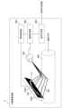
- FIG. 1 is a diagram schematically showing the configuration of a visual inspection apparatus 1 according to Embodiment 1.
- the visual inspection apparatus 1 has an illumination 100 , an illumination control section 200 , an imaging device 300 , an image acquisition section 400 and a pass/fail determination section 500 .
- the appearance inspection apparatus 1 inspects the appearance of the surface of an object 600 to be inspected.
- the appearance inspection apparatus 1 can diagnose an abnormality related to the appearance of the surface of the object 600 to be inspected. In other words, the visual inspection apparatus 1 can diagnose an abnormality related to the shape or state of the surface of the object 600 to be inspected.
- the illumination 100 has a light source that emits light such as visible light, infrared rays, and ultraviolet rays.
- the illumination 100 illuminates the inspected object 600 .
- lighting 100 has a region 110 that emits light.
- the light-emitting region 110 is also referred to as a “light-emitting region”.
- the lighting control unit 200 controls the lighting 100. That is, the lighting control unit 200 is a device that controls turning on and off of the lighting 100 . Therefore, the illumination 100 emits light under the control of the illumination control section 200 .
- the imaging device 300 images the object 600 to be inspected.
- the imaging device 300 images the inspected object 600 being transported.
- the imaging device 300 is, for example, a line camera.
- the imaging device 300 may be a device that acquires an image using only pixels corresponding to a specific row using an area camera.
- the image acquisition unit 400 acquires an image of the subject 600 from the imaging device 300 .
- the image acquisition unit 400 controls the imaging device 300 to acquire an image of the inspection object 600 .
- the image acquisition unit 400 can send the image of the inspection object 600 to the quality determination unit 500 .
- the pass/fail determination unit 500 acquires the image of the inspection object 600 from the image acquisition unit 400 .
- the pass/fail judgment unit 500 performs image processing on the image of the inspection object 600, judges the pass/fail of the appearance of the inspection object 600, and outputs the pass/fail judgment result.
- the object 600 to be inspected has a curved surface.
- the device under test 600 has the same surface shape with respect to a specific direction and is formed by a plurality of normal directions.
- the inspected object 600 is, for example, a handrail for an escalator, a guide rail for an elevator, a rail for a railroad, a trolley, or the like.
- the inspected object 600 is inspected while being transported in a direction orthogonal to the cross section having the same surface shape.
- a region 110 in which the illumination 100 emits light is a region in which light is emitted from the illumination 100 toward the inspection object 600 .
- the light emitting area 110 of the illumination 100 is determined based on the state of the surface of the inspection object 600 so that the imaging device 300 detects either specularly reflected light or diffusely reflected light.
- the light-emitting area 110 of the illumination 100 is determined based on the state of the surface of the inspection object 600 so that the imaging device 300 detects specularly reflected light.
- the state of the surface of the object to be inspected 600 is, for example, a shape such as unevenness.
- the light-emitting region 110 of the illumination 100 is determined based on the state of the surface of the inspection object 600 so that the imaging device 300 detects specularly reflected light and does not detect diffusely reflected light. area.
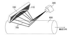
- the region 110 where the illumination 100 emits light is the region where the illumination 100 intersects with the chief ray 700 incident on the pixels of the imaging device 300 when reflected by specular reflection on the object 600 to be inspected. be.
- the area where the principal ray 700 incident on the pixels of the imaging device 300 when reflected by specular reflection on the test object 600 and the illumination 100 do not intersect is the non-light emitting area of the illumination 100. is. That is, in the example shown in FIG. 1, the imaging device 300 detects specularly reflected light and does not detect diffusely reflected light.
- a chief ray 700 is a ray that passes through the center of the aperture of the imaging device 300 .
- the chief ray 700 is the ray that passes through the center of the entrance pupil of the imaging device 300 . Since the principal ray 700 is light, when it is incident on the object 600 to be inspected, it is reflected by the object 600 to be inspected.
- the illumination 100 may have a light shielding material that shields light from the illumination 100 (specifically, the light source).
- the light shielding material is, for example, a metal material.
- a light shielding material is provided in a region of the illumination 100 other than the light emitting region 110 . That is, the light shielding material is provided in the non-light emitting area of the lighting 100 .
- the light emitting region 110 of the illumination 100 is configured.
- the light-emitting region 110 is determined, for example, by experiments, simulations, or both. Examples of methods for determining the light emitting region 110 are described below.
- the light emitting area 110 of the illumination 100 is determined by, for example, a ray tracing method.
- a ray tracing method An example of a method for determining the light emitting region 110 by simulation will be described.
- a chief ray 700 incident on a pixel of the imaging device 300 is calculated by a method such as a ray tracing method.
- a portion where the calculated chief ray 700 and the illumination 100 intersect is defined as a light emitting region 110 .
- the configuration may be such that the shape information of the object 600 to be inspected is acquired. Further, the configuration may be such that information regarding the positional relationship between the illumination 100, the imaging device 300, and the inspection object 600 is acquired. It may be configured to acquire design information of an optical system such as lens design of the imaging device 300 .
- This method first determines the light emitting region 110 by simulation. Next, an image of the inspected object 600 is obtained using the determined light emitting region 110 . In this case, if there are some pixels for which specular reflection light cannot be obtained due to the difference between the calculation conditions and the actual conditions, the light-emitting region 110 is adjusted. Through the above procedure, the light-emitting region 110 can be determined with high accuracy.
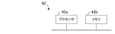
- FIG. 2 is a diagram showing an example of the hardware configuration of the control unit 42.
- FIG. 3 is a diagram showing another example of the hardware configuration of the control unit 42. As shown in FIG.
- the illumination control unit 200, the image acquisition unit 400, and the quality determination unit 500 are configured by the control unit 42, for example.
- the control unit 42 is composed of, for example, at least one processor 42a and at least one memory 42b.
- the processor 42a is, for example, a CPU (Central Processing Unit) that executes programs stored in the memory 42b.
- the functions of the illumination control unit 200, the image acquisition unit 400, and the quality determination unit 500 are implemented by software, firmware, or a combination of software and firmware.
- Software and firmware can be stored in memory 42b as programs. With this configuration, a computer executes a program for realizing the functions of the control unit 42 .
- the memory 42b is a computer-readable recording medium, for example, volatile memory such as RAM (Random Access Memory) and ROM (Read Only Memory), nonvolatile memory, or a combination of volatile and nonvolatile memory. is.
- the control unit 42 may have multiple processors 42a and multiple memories 42b. In this case, the functions of the illumination control unit 200, the image acquisition unit 400, and the quality determination unit 500 are realized by these multiple processors 42a and multiple memories 42b.
- the control unit 42 may be configured with a processing circuit 42c as dedicated hardware such as a single circuit and a composite circuit.
- the processing circuit 42c is, for example, a system LSI. In this case, the functions of the illumination control unit 200, the image acquisition unit 400, and the quality determination unit 500 are realized by the processing circuit 42c.
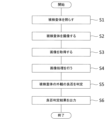
- FIG. 4 is a flow chart showing an example of a visual inspection method for inspecting the object 600 to be inspected.
- the visual inspection method for inspecting the appearance of the surface of an object 600 to be inspected includes step S1 of illuminating the object 600 with the illumination 100 and step S2 of imaging the object 600 with the imaging device 300. a step S3 for acquiring an image of the inspection object 600; a step S4 for performing image processing on the image acquired in step S3; a step S5 for judging whether the appearance of the inspection object 600 is good or bad; and a step S6 of outputting the result.
- the area 110 where the illumination 100 emits light is determined based on the state of the surface of the inspection object 600 so that the imaging device 300 detects either specular reflected light or diffuse reflected light.
- the light-emitting area 110 of the illumination 100 is determined based on the state of the surface of the inspection object 600 so that the imaging device 300 detects only specularly reflected light.
- the object 600 to be inspected is, for example, a cylindrical extruded product. That is, the object to be inspected is a cylindrical extruded product.
- the extruded product is conveyed, for example, in a direction perpendicular to the cross section having the same surface shape.
- the object to be inspected 600 is not limited to a cylindrical shape, and may have an elliptical shape as long as it has the same surface shape in one direction. may be
- step S1 the illumination 100 emits light under the control of the illumination control unit 200.
- a light emitting region 110 is a region where the principal ray 700 incident on the pixels of the imaging device 300 and the illumination 100 intersect.
- step S2 the imaging device 300 is controlled by the image acquisition section 400 to image the object 600 to be inspected.
- step S3 the image acquisition unit 400 acquires an image captured by the imaging device 300.
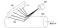
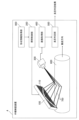
- FIG. 5 is a diagram showing a state in which a normal portion of the surface of the object 600 to be inspected is imaged.
- the entire surface of the subject 600 is normal.
- a normal part means a part manufactured according to design and having no abnormality.
- all of the chief rays 700 incident on the pixels of the imaging device 300 intersect the emitting region 110 . Therefore, specular reflected light is detected in all pixels of the imaging device 300, and the brightness is increased.
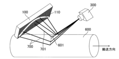
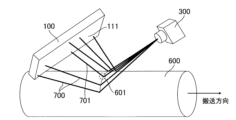
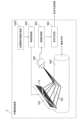
- FIG. 6 is a diagram showing a state in which an abnormal portion 601 on the surface of an object 600 to be inspected is imaged.
- an abnormal portion 601 exists on a portion of the surface of an object 600 to be inspected.
- the abnormal portion 601 means a portion that is not manufactured as designed and has irregularities or the like.
- the ray is reflected in a direction different from that when incident on the normal portion. be. Therefore, specular reflected light is not detected in the pixels of the imaging device 300 that captures an image of the abnormal portion 601, so the luminance is low. That is, the brightness detected by the imaging device 300 is high in normal portions and low in abnormal portions.
- FIG. 7 is a diagram showing a state in which a normal portion of the surface of an object to be inspected 600 is imaged by a visual inspection apparatus as a comparative example.
- the entire surface facing the inspected object 600 is the region 111 that emits light. All of the principal rays 700 incident on the pixels of the imaging device 300 intersect the illumination 100, so specular reflected light is detected in all the pixels of the imaging device 300 and the brightness increases.
- FIG. 8 is a diagram showing a state in which an abnormal portion 601 on the surface of an object 600 to be inspected is imaged by a visual inspection apparatus as a comparative example. Since the principal ray including the principal ray 701 that is incident on the abnormal portion and whose reflection direction is different from that of the normal portion intersects the illumination 100, the specularly reflected light is detected in all the pixels of the imaging device 300, and the luminance is get higher That is, in the comparative example, the brightness detected by the imaging device 300 is high even in the abnormal portion, so there is no difference between the normal portion and the abnormal portion.
- the pass/fail judgment unit 500 performs image processing on the image received from the image acquisition unit 400, judges the pass/fail of the appearance of the inspection object 600, and outputs the pass/fail judgment result.
- the pass/fail determination unit 500 can determine whether or not there is a change in brightness by comparing surrounding pixels using an image processing algorithm such as a differential filter, and can determine that a portion with a change is abnormal.
- the pass/fail judgment section 500 cannot judge whether the image is normal or abnormal.
- the light-emitting area 110 of the illumination 100 is determined based on the state of the surface of the inspection object 600 so that the imaging device 300 detects only specularly reflected light. Therefore, in the image captured by the imaging device 300, the normal portion has high brightness and the abnormal portion has low brightness, resulting in a difference in brightness between the normal portion and the abnormal portion. As a result, the quality determination accuracy of the quality determining unit 500 is improved, and the inspection accuracy for the device under test 600 can be improved.
- the illumination 100 has a light shielding material that shields the light from the illumination 100 (specifically, the light source), the light emitting region 110 can be easily formed.
- a light blocking material may be attached to an off-the-shelf lighting fixture. In this case, the cost of lighting 100 can be reduced.
- a configuration for acquiring shape information of the inspection object 600 when determining the light emitting region 110 by simulation, a configuration for acquiring shape information of the inspection object 600, a configuration for acquiring information on the positional relationship between the illumination 100, the imaging device 300, and the inspection object 600, and an imaging
- a configuration for acquiring optical system design information such as the lens design of the device 300
- the light-emitting region 110 may be determined in consideration of manufacturing tolerances of the device 600 to be inspected. As a result, even if the position of the principal ray 700 varies due to manufacturing tolerances of the object 600 to be inspected, the light emitting region 110 can be determined so that the principal ray 700 intersects the light emitting region 110 . Therefore, even if there is a manufacturing tolerance on the surface of the object to be inspected 600, the brightness of the image does not change, so false detection can be reduced.
- the lighting 100 may have a linear light source. As a result, the number of light-emitting elements is smaller than that of planar lighting, so the cost of the lighting can be reduced.
- FIG. 9 is a diagram schematically showing the configuration of an appearance inspection apparatus 1A as a modified example.
- a visual inspection apparatus 1A as a modification differs from the visual inspection apparatus 1 shown in FIG. 1 in that a fixing member 800 is further provided.
- the fixing member 800 fixes the positional relationship among the illumination 100 , imaging device 300 and inspection object 600 .
- the fixing member 800 can set the positional relationship among the imaging device 300 , the illumination 100 , and the inspection object 600 to a preset condition.
- the fixing member 800 fixes the illumination 100 and the imaging device 300.
- the fixing member 800 has a portion that contacts the device under test 600 at a predetermined position. Thereby, the positional relationship between the imaging device 300, the illumination 100, and the inspection object 600 can be set to a preset positional relationship.
- rollers or bearings may be used so as not to damage the object 600 to be inspected.
- the fixing member 800 may be fixed to a structure around the inspection object 600 to set the positional relationship of the imaging device 300, the illumination 100, and the inspection object 600 to a predetermined condition. With this configuration, it is possible to easily adjust the positional relationship among the illumination 100, the imaging device 300, and the inspection object 600 to a predetermined condition, and reduce work costs related to position adjustment.
- the visual inspection apparatus 1A may further have a darkroom (not shown) that shields external light.
- a darkroom (not shown) that shields external light.
- the lighting 100, the imaging device 300, and the test object 600 are covered by a darkroom.
- the imaging device 300 does not detect unnecessary external light, inspection accuracy can be further improved.
- the darkroom the entire room may be shielded from light, a dark box may be used, or the illumination 100, the imaging device 300, and the subject 600 may be shielded with a light-shielding curtain or a light-shielding curtain. You may
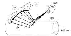
- FIG. 10 is a diagram schematically showing the configuration of a visual inspection apparatus 2 according to Embodiment 2.
- the visual inspection apparatus 2 has an illumination 101 , an illumination control section 201 , an imaging device 300 , an image acquisition section 400 and a pass/fail determination section 501 .
- the lighting 101 is different from the lighting 100 of the visual inspection apparatus 1 according to the first embodiment.
- the position of the light-emitting region 112 of the illumination 101 is different from the light-emitting region 110 of the illumination 100 of the visual inspection apparatus 1 according to the first embodiment.
- the lighting 101 has a light source that emits light such as visible light, infrared rays, and ultraviolet rays.
- the illumination 101 illuminates the inspected object 600 .
- illumination 101 has a region 112 that emits light.
- the light-emitting region 112 is also referred to as a "light-emitting region”.
- the illumination control unit 200, imaging device 300, and image acquisition unit 400 are the same as in the first embodiment.
- the pass/fail determination unit 501 acquires the image of the inspection object 600 from the image acquisition unit 400 .
- the pass/fail determination unit 501 performs image processing on the image of the inspection object 600, determines the pass/fail of the appearance of the inspection object 600, and outputs the pass/fail determination result.
- the light-emitting region 112 is different from the light-emitting region 110 in the first embodiment, so the content of the image processing does not necessarily match the content of the image processing in the first embodiment.
- a region 112 where the illumination 101 emits light is a region where light is emitted from the illumination 101 toward the inspection object 600 .
- the region 112 where the illumination 101 emits light is a region determined based on the state of the surface of the object 600 to be inspected so that the imaging device 300 detects diffusely reflected light and does not detect specularly reflected light. is.
- the region 112 where the illumination 101 emits light is a region where the illumination 101 does not intersect with the principal ray 700 incident on the pixels of the imaging device 300 when specularly reflected on the object 600 to be inspected.
- the imaging device 300 detects diffusely reflected light and does not detect specularly reflected light.
- the illumination 101 may have a light shielding material that shields light from the illumination 101 (specifically, the light source).
- the light shielding material is, for example, a metal material.
- a light shielding material is provided in a region of the illumination 100 other than the light emitting region 112 . That is, a light shielding material is provided in the non-light emitting area of the illumination 101 . As a result, the light-emitting region 112 of the illumination 101 is formed.
- the light-emitting region 112 is determined, for example, by experiments, simulations, or both. Examples of methods for determining the light emitting region 112 are described below.
- a chief ray 700 incident on a pixel of the imaging device 300 is calculated by a method such as a ray tracing method.
- a portion where the calculated chief ray 700 and the illumination 101 do not intersect is a light emitting region 112 .
- the appearance inspection apparatus 2 may be configured to acquire the shape information of the inspected object 600.
- the appearance inspection apparatus 2 may be configured to acquire information regarding the positional relationship between the lighting 100 , the imaging device 300 and the inspection object 600 .
- the appearance inspection apparatus 2 may be configured to acquire design information of an optical system such as lens design of the imaging device 300 .
- This method first determines the light emitting region 112 by simulation. Next, an image of the inspected object 600 is acquired using the determined light-emitting region 112 . In this case, if there are some pixels that acquire specularly reflected light due to the difference between the calculation conditions and the actual conditions, the light-emitting region 112 is adjusted. Through the above procedure, the light-emitting region 112 can be determined with high accuracy.
- a visual inspection method for inspecting the appearance of the surface of an object 600 to be inspected includes, as shown in FIG. a step S3 for acquiring an image of the inspection object 600; a step S4 for performing image processing on the image acquired in step S3; a step S5 for judging whether the appearance of the inspection object 600 is good or bad; and a step S6 of outputting the result.
- the light-emitting region 110 of the illumination 100 is determined based on the state of the surface of the inspection object 600 so that the imaging device 300 detects only diffusely reflected light.
- the object 600 to be inspected is, for example, a cylindrical extruded product. That is, the object to be inspected is a cylindrical extruded product.
- the extruded product is conveyed, for example, in a direction perpendicular to the cross section having the same surface shape.
- step S1 the lighting 101 emits light under the control of the lighting control unit 200.
- a light emitting region 112 is a region where the chief ray 700 incident on the pixels of the imaging device 300 and the illumination 101 do not intersect.
- step S2 the imaging device 300 is controlled by the image acquisition section 400 to image the object 600 to be inspected.
- step S3 the image acquisition unit 400 acquires the image captured by the imaging device 300.
- FIG. 11 is a diagram showing a state in which a normal portion of the surface of the object 600 to be inspected is imaged.
- the entire surface of the test object 600 is normal.
- a normal part means a part manufactured according to design and having no abnormality.
- not all of the chief rays 700 incident on the pixels of the imaging device 300 intersect the emitting regions 112 . Therefore, the specular reflected light is not detected in all the pixels of the imaging device 300, and the luminance becomes low.
- FIG. 12 is a diagram showing a state in which an abnormal portion 601 on the surface of an object 600 to be inspected is imaged.
- an abnormal portion 601 exists on part of the surface of an object 600 to be inspected.
- the abnormal portion 601 means a portion that is not manufactured as designed and has irregularities or the like.
- the ray is reflected in a direction different from when incident on the normal portion. Therefore, the principal ray incident on the abnormal portion 601 and reaching the imaging device 300 is the principal ray 701 that intersects the light emitting region 112 . . Therefore, diffusely reflected light is detected in the pixels of the imaging device 300 that captures an image of the abnormal portion 601, so that the luminance increases. That is, the brightness detected by the imaging device 300 is low in normal portions and high in abnormal portions.
- the pass/fail judgment unit 501 performs image processing on the image received from the image acquisition unit 400, judges the pass/fail of the appearance of the inspection object 600, and outputs the pass/fail judgment result.
- the pass/fail determination unit 500 can determine whether or not there is a change in brightness by comparing surrounding pixels using an image processing algorithm such as a differential filter, and can determine that a portion with a change is abnormal.
- the light-emitting region 112 of the illumination 101 is determined based on the state of the surface of the inspection object 600 so that the imaging device 300 detects only diffusely reflected light. Therefore, in the image captured by the imaging device 300, normal portions have low brightness and abnormal portions have high brightness, resulting in a difference in brightness between the normal portion and the abnormal portion. As a result, the quality determination accuracy of the quality determining unit 500 is improved, and the inspection accuracy for the device under test 600 can be improved.
- the illumination 101 has a light shielding material that shields the light from the illumination 101 (specifically, the light source), the light-emitting region 112 can be easily formed.
- a light blocking material may be attached to an off-the-shelf lighting fixture. In this case, the cost of lighting 101 can be reduced.
- a configuration for acquiring shape information of the inspection object 600 a configuration for acquiring information on the positional relationship between the illumination 101, the imaging device 300, and the inspection object 600, an imaging
- a configuration for acquiring optical system design information such as the lens design of the device 300
- the light-emitting region 112 may be determined in consideration of manufacturing tolerances of the device under test 600 . Thus, even if the position of the principal ray 700 varies due to manufacturing tolerances of the object 600 to be inspected, the light emitting region 112 can be determined so that the principal ray 700 does not cross the light emitting region 112 . Therefore, even if there is a manufacturing tolerance on the surface of the object to be inspected 600, the brightness of the image does not change, so false detection can be reduced.
- the visual inspection apparatus 2 may further include a darkroom that shields external light.
- the lighting 101, the imaging device 300, and the test object 600 are covered by a dark room.
- FIG. 13 is a diagram schematically showing the configuration of a visual inspection apparatus 3 according to Embodiment 3.
- the visual inspection apparatus 3 includes an illumination 102 , an illumination control section 202 , an imaging device 300 , an image acquisition section 400 , and a pass/fail determination section 500 .
- the lighting 102 has a plurality of light emitting elements 102A. Each light emitting element 102A can emit visible light, infrared light, or ultraviolet light. With this configuration, the illumination 102 illuminates the inspected object 600 . In this embodiment, illumination 102 has a region 113 that emits light. The light-emitting region 113 is also called a “light-emitting region”. Illumination 102 is, for example, a display.
- the lighting control unit 202 is a device that controls lighting and extinguishing of each light emitting element 102A of the lighting 102 . That is, each of the plurality of light emitting elements 102A is controlled by the illumination control section 202. FIG. Therefore, the lighting 102 emits light under the control of the lighting control section 202 .
- the imaging device 300, the image acquisition unit 400, and the quality determination unit 500 are the same as those described in the first embodiment.
- a region 113 where the illumination 102 emits light is a region where light is emitted from the illumination 102 toward the inspection object 600 .
- the light-emitting region 113 of the lighting 102 is a region formed by the lit light-emitting elements 102A among the plurality of light-emitting elements 102A.
- the light-emitting elements 102A to be lit are determined based on the image of the inspected object 600 resulting from lighting of the plurality of light-emitting elements 102A.
- the light-emitting region 113 is determined based on the state of the surface of the inspection object 600 so that the imaging device 300 detects specularly reflected light and does not detect diffusely reflected light. be.
- the light-emitting region 113 is determined, for example, by experiments, simulations, or both. Examples of methods for determining the light emitting region 110 are described below.
- Embodiment 1 An example of a method for determining the light-emitting region 113 by experiment will be described.
- the method shown in Embodiment 1 can be automated.
- N and M are natural numbers.
- an image of the inspected object 600 is acquired under the condition that only each area of the N ⁇ M area is illuminated while switching pixels to emit light in a predetermined pattern. In this case, it is checked by image processing whether there is an area where high brightness is obtained in the image acquired under each condition. If there is a region with high luminance, it is assumed that the region intersects with the principal ray 700 and is defined as a light-emitting region 113 .
- the area is excluded from the light-emitting area 113 as not intersecting with the principal ray 700 .
- the light-emitting area 113 in the illumination 102 can be automatically determined.
- the light-emitting region 113 can be determined by the method described in the first embodiment.
- the inspected object 600 is, for example, a cylindrical extruded product. That is, the object to be inspected is a cylindrical extruded product.
- the extruded product is conveyed, for example, in a direction perpendicular to the cross section having the same surface shape.
- the lighting 102 emits light under the control of the lighting control unit 202 .
- a light emitting region 113 is a region where the chief ray 700 incident on the pixels of the imaging device 300 and the illumination 102 intersect.
- the imaging device 300 is controlled by the image acquisition unit 400 and images the object 600 to be inspected.
- the image acquisition unit 400 acquires the image captured by the imaging device 300 .
- the brightness detected by the imaging device 300 is high in normal portions and low in abnormal portions.
- the pass/fail judgment unit 500 performs image processing on the image received from the image acquisition unit 400, judges the pass/fail of the appearance of the inspection object 600, and outputs the pass/fail judgment result. As described in the first embodiment, the pass/fail judgment unit 500 judges normality or abnormality by an image processing algorithm such as a differential filter, and outputs a pass/fail judgment result.
- an image processing algorithm such as a differential filter
- the visual inspection apparatus 3 according to the third embodiment has the advantages described in the first embodiment.
- a device capable of controlling the lighting of each light emitting element 102A can be used as the lighting 102, so custom-made lighting is unnecessary. As a result, the cost of the appearance inspection device 3 can be reduced.
- the region 113 to emit light when determining the region 113 to emit light, an image is acquired while each light emitting element 102A to be lit is changed, and whether or not each light emitting element 102A contributes to specular reflection is automatically determined. can be determined Therefore, it is possible to determine the light-emitting region 113 at low cost without performing a simulation or experimentally verifying a plurality of light-emitting regions 113 prepared.
- the light-emitting region 113 is a region determined to detect specularly reflected light. , may be an area determined to detect diffusely reflected light.
- FIG. 14 is a diagram schematically showing the configuration of a visual inspection apparatus 4 according to Embodiment 4.
- the visual inspection apparatus 4 includes an illumination 100 having a light emitting area 110 , an illumination control section 200 , an imaging device 300 , an image acquisition section 400 , a pass/fail determination section 500 , and a shape information acquisition section 900 .
- a visual inspection apparatus 4 according to Embodiment 4 differs from the visual inspection apparatus 1 according to Embodiment 1 in that it further includes a shape information acquisition section 900 .
- the area 110 where the illumination 100 emits light is an area determined based on the information acquired by the shape information acquiring section 900 .
- the shape information acquisition unit 900 acquires information about the shape of the surface of the object 600 to be inspected.
- the light emitting area 110 of the illumination 100 is determined based on the information acquired by the shape information acquiring section 900 .
- FIG. 15 is a diagram schematically showing the configuration of a visual inspection apparatus 5 as Modification 1 of Embodiment 4.
- the visual inspection apparatus 5 includes an illumination 100 having a light emitting area 110 , an illumination control section 200 , an imaging device 300 , an image acquisition section 400 , a pass/fail determination section 500 , and a positional relationship information acquisition section 1000 . It differs from the visual inspection apparatus 1 of the embodiment in that a positional relationship information acquisition unit 1000 is added.
- the area 110 where the illumination 100 emits light is an area determined based on the information acquired by the positional relationship information acquiring section 1000 .
- the positional relationship information acquisition unit 1000 acquires information on the position of the object 600 to be inspected.
- a region 110 in which the illumination 100 emits light is determined based on the information acquired by the positional relationship information acquiring section 1000 .
- the light emitting area 110 of the illumination 100 for detecting either the specularly reflected light or the diffusely reflected light is determined. can do.
- FIG. 16 is a diagram schematically showing the configuration of a visual inspection apparatus 6 as Modification 2 of Embodiment 4.
- the visual inspection apparatus 6 includes an illumination 100 having a light emitting area 110 , an illumination control section 200 , an imaging device 300 , an image acquisition section 400 , a pass/fail determination section 500 , and a manufacturing tolerance information acquisition section 1100 . It differs from the visual inspection apparatus 1 of the embodiment in that a manufacturing tolerance information acquisition unit 1100 is added.
- light emitting region 110 of illumination 100 is a region determined based on information acquired by manufacturing tolerance information acquisition section 1100 .
- the manufacturing tolerance information acquisition unit 1100 acquires information on the manufacturing tolerance of the inspection object 600 .
- the light emitting area 110 of the illumination 100 is determined based on the information acquired by the manufacturing tolerance information acquisition unit 1100 . By determining the region 110 in which the illumination 100 emits light in consideration of the manufacturing tolerance information of the inspected object 600, luminance change caused by the manufacturing tolerance does not occur and erroneous detection can be reduced.
- FIG. 17 is a diagram schematically showing the configuration of a visual inspection apparatus 7 as Modified Example 3 of Embodiment 4.
- the visual inspection apparatus 7 includes an illumination 100 having a light emitting area 110 , an illumination control section 200 , an imaging device 300 , an image acquisition section 400 , a quality determination section 500 , and an imaging device information acquisition section 1200 . It differs from the appearance inspection apparatus 1 of the embodiment in that an imaging device information acquisition unit 1200 is added.
- the illumination emitting region 110 is a region determined based on the information acquired by the imaging device information acquiring section 1200 .
- the imaging device information acquisition unit 1200 acquires information regarding the optical system of the imaging device 300 .
- the light emitting area 110 of the lighting 100 is determined based on the information acquired by the imaging device information acquiring section 1200 .
- By obtaining information about the optical system of the imaging device 300 it is possible to determine the light emitting area 120 of the illumination 100 for detecting only one of specularly reflected light and non-specularly reflected light.
- Appearance inspection device 100, 101 lighting, 110, 112, 113 emitting area, 200, 202 lighting control unit, 300 imaging device, 400 image acquisition unit, 500, 501 Pass/fail determination unit 600 Inspection object 700 Chief ray 900 Shape information acquisition unit 1000 Positional relationship information acquisition unit 1100 Manufacturing tolerance information acquisition unit 1200 Imaging device information acquisition unit.
Landscapes
- Physics & Mathematics (AREA)
- Health & Medical Sciences (AREA)
- Life Sciences & Earth Sciences (AREA)
- Chemical & Material Sciences (AREA)
- Analytical Chemistry (AREA)
- Biochemistry (AREA)
- General Health & Medical Sciences (AREA)
- General Physics & Mathematics (AREA)
- Immunology (AREA)
- Pathology (AREA)
- Investigating Materials By The Use Of Optical Means Adapted For Particular Applications (AREA)
Abstract
Description
被検査体の表面の外観を検査する外観検査装置であって、
前記被検査体を照らす照明と、
前記照明を制御する照明制御部と、
前記被検査体を撮像する撮像デバイスと、
前記撮像デバイスから前記被検査体の画像を取得する画像取得部と、
前記画像に対して画像処理を行い、前記被検査体の前記外観の良否を判定し、良否判定結果を出力する良否判定部と、を備え、
前記照明の発光する領域は、前記被検査体の前記表面の状態に基づいて、前記撮像デバイスが鏡面反射光又は拡散反射光のいずれか一方を検出するように決定される。
本開示の外観検査方法は、
被検査体の表面の外観を検査する外観検査方法であって、
照明によって前記被検査体を照らすステップと、
撮像デバイスによって前記被検査体を撮像するステップと、
前記被検査体の画像を取得するステップと、
前記画像に対して画像処理を行うステップと、
前記被検査体の前記外観の良否を判定するステップと、
良否判定結果を出力するステップと、を備え、
前記照明の発光する領域は、前記被検査体の前記表面の状態に基づいて、前記撮像デバイスが鏡面反射光又は拡散反射光のいずれか一方を検出するように決定される。
実施の形態1.
実施の形態1に係る外観検査装置1の構成について説明する。
図1は、実施の形態1に係る外観検査装置1の構成を概略的に示す図である。
外観検査装置1は、照明100と、照明制御部200と、撮像デバイス300と、画像取得部400と、良否判定部500とを有する。外観検査装置1は、被検査体600の表面の外観を検査する。外観検査装置1は、被検査体600の表面の外観に関する異常を診断することができる。言い換えると、外観検査装置1は、被検査体600の表面の形状又は状態に関する異常を診断することができる。
図3は、制御部42のハードウェア構成の他の例を示す図である。
図4は、被検査体600を検査する外観検査方法の一例を示すフローチャートである。
図4に示される例では、被検査体600の表面の外観を検査する外観検査方法は、照明100によって被検査体600を照らすステップS1と、撮像デバイス300によって被検査体600を撮像するステップS2と、被検査体600の画像を取得するステップS3と、ステップS3で取得された画像に対して画像処理を行うステップS4と、被検査体600の外観の良否を判定するステップS5と、良否判定結果を出力するステップS6とを含む。この外観検査方法において、照明100の発光する領域110は、被検査体600の表面の状態に基づいて、撮像デバイス300が鏡面反射光又は拡散反射光のいずれか一方を検出するように決定される。本実施の形態では、照明100の発光する領域110は、被検査体600の表面の状態に基づいて、撮像デバイス300が鏡面反射光のみを検出するように決定される。
正常部分とは、設計通りに製造された、異常のない部分を意味する。図5に示される例では、撮像デバイス300の画素に入射する主光線700の全ては、発光する領域110と交差する。したがって、撮像デバイス300の全ての画素において鏡面反射光が検出され、輝度は高くなる。
異常部分601とは、設計通りに製造されず、凹凸等が発生している部分を意味する。異常部分601では、正常部分に入射した場合とは異なる方向に光線が反射するので、異常部分601へ入射し撮像デバイス300に到達する主光線は、発光する領域110とは交差しない主光線701である。したがって、異常部分601を撮像する撮像デバイス300の画素において鏡面反射光は検出されないため、輝度は低くなる。すなわち、撮像デバイス300によって検出される輝度は、正常部分では高くなり、異常部分では低くなる。
図7は、比較例としての外観検査装置において被検査体600の表面の正常部分を撮像している状態を示す図である。
比較例としての外観検査装置の照明100では、被検査体600に対向する面の全てが発光する領域111である。撮像デバイス300の画素に入射する主光線700の全ては、照明100に交差するため、撮像デバイス300の全ての画素において鏡面反射光が検出され、輝度は高くなる。
異常部分に入射して反射方向が正常部分のときとは異なる主光線701も含めて、主光線は照明100に交差するため、撮像デバイス300の全ての画素において鏡面反射光が検出され、輝度は高くなる。すなわち、比較例において、撮像デバイス300によって検出される輝度は、異常部分でも高くなるため、正常部分と異常部分との間で差異が生じない。
本実施の形態によれば、照明100の発光する領域110は、被検査体600の表面の状態に基づいて、撮像デバイス300が鏡面反射光のみを検出するように決定される。したがって、撮像デバイス300によって撮像された画像において、正常部分は高い輝度となり、異常部分は低い輝度となり、正常部分と異常部分との間で輝度に差異が生じる。その結果、良否判定部500の良否判定の精度が向上し、被検査体600に対する検査精度を向上させることができる。
図9は、変形例としての外観検査装置1Aの構成を概略的に示す図である。
変形例としての外観検査装置1Aは、固定部材800をさらに備える点で、図1に示される外観検査装置1と異なる。固定部材800は、照明100、撮像デバイス300、及び被検査体600の間の位置関係を固定する。これにより、固定部材800は、撮像デバイス300と、照明100と、被検査体600との位置関係を予め設定した条件にすることができる。図9に示される例では、固定部材800は、照明100及び撮像デバイス300を固定している。さらに、固定部材800は、予め定められた位置で被検査体600と接触する部分を有する。これにより、撮像デバイス300と、照明100と、被検査体600との位置関係を予め設定された位置関係に設定することができる。
実施の形態2に係る外観検査装置2の構成について説明する。
図10は、実施の形態2に係る外観検査装置2の構成を概略的に示す図である。
外観検査装置2は、照明101と、照明制御部201と、撮像デバイス300と、画像取得部400と、良否判定部501とを有する。実施の形態2に係る外観検査装置2では、照明101が実施の形態1に係る外観検査装置1の照明100と異なる。具体的には、照明101の発光する領域112の位置が、実施の形態1に係る外観検査装置1の照明100の発光する領域110と異なる。
被検査体600の表面の外観を検査する外観検査方法は、図4に示されるように、照明100によって被検査体600を照らすステップS1と、撮像デバイス300によって被検査体600を撮像するステップS2と、被検査体600の画像を取得するステップS3と、ステップS3で取得された画像に対して画像処理を行うステップS4と、被検査体600の外観の良否を判定するステップS5と、良否判定結果を出力するステップS6とを含む。本実施の形態では、照明100の発光する領域110は、被検査体600の表面の状態に基づいて、撮像デバイス300が拡散反射光のみを検出するように決定される。
正常部分とは、設計通りに製造された、異常のない部分を意味する。図11に示される例では、撮像デバイス300の画素に入射する主光線700の全てが、発光する領域112と交差しない。したがって、撮像デバイス300の全ての画素において鏡面反射光が検出されず、輝度は低くなる。
異常部分601とは、設計通りに製造されず、凹凸等が発生している部分を意味する。異常部分601では、正常部分に入射した場合とは異なる方向に光線が反射するので、異常部分601へ入射し撮像デバイス300に到達する主光線は、発光する領域112と交差する主光線701である。したがって、異常部分601を撮像する撮像デバイス300の画素において、拡散反射光が検出されるため、輝度は高くなる。すなわち、撮像デバイス300によって検出される輝度は、正常部分では低くなり、異常部分では高くなる。
本実施の形態によれば、照明101の発光する領域112は、被検査体600の表面の状態に基づいて、撮像デバイス300が拡散反射光のみを検出するように決定される。したがって、撮像デバイス300によって撮像された画像において、正常部分は低い輝度となり、異常部分は高い輝度となり、正常部分と異常部分との間で輝度に差異が生じる。その結果、良否判定部500の良否判定の精度が向上し、被検査体600に対する検査精度を向上させることができる。
実施の形態3に係る外観検査装置3の構成について説明する。
図13は、実施の形態3に係る外観検査装置3の構成を概略的に示す図である。
外観検査装置3は、照明102と、照明制御部202と、撮像デバイス300と、画像取得部400と、良否判定部500と、から構成される。
被検査体600は、例えば、円筒状の押出成形品である。すなわち、被検査対象が、円筒状の押出成形品である。被検査体600を検査するとき、この押出成形品は、例えば、同一の表面形状を有する断面と直交する方向に搬送される。
実施の形態3に係る外観検査装置3は、実施の形態1に記載の利点を有する。
実施の形態4に係る外観検査装置4の構成について説明する。
図14は、実施の形態4に係る外観検査装置4の構成を概略的に示す図である。
外観検査装置4は、発光する領域110を有する照明100と、照明制御部200と、撮像デバイス300と、画像取得部400と、良否判定部500と、形状情報取得部900とを有する。実施の形態4に係る外観検査装置4は、形状情報取得部900をさらに有する点で実施の形態1に係る外観検査装置1と異なる。実施の形態4では、照明100の発光する領域110は、形状情報取得部900によって取得された情報に基づいて決定された領域である。
図15は、実施の形態4の変形例1としての外観検査装置5の構成を概略的に示す図である。
外観検査装置5は、発光する領域110を有する照明100と、照明制御部200と、撮像デバイス300と、画像取得部400と、良否判定部500と、位置関係情報取得部1000とを有する。位置関係情報取得部1000が追加された点が実施の形態の外観検査装置1と異なる。実施の形態4の変形例1では、照明100の発光する領域110は、位置関係情報取得部1000によって取得された情報に基づいて決定された領域である。
図16は、実施の形態4の変形例2としての外観検査装置6の構成を概略的に示す図である。
外観検査装置6は、発光する領域110を有する照明100と、照明制御部200と、撮像デバイス300と、画像取得部400と、良否判定部500と、製造公差情報取得部1100とを有する。製造公差情報取得部1100が追加された点が実施の形態の外観検査装置1と異なる。実施の形態4の変形例2では、照明100の発光する領域110は、製造公差情報取得部1100によって取得された情報に基づいて決定された領域である。
図17は、実施の形態4の変形例3としての外観検査装置7の構成を概略的に示す図である。
外観検査装置7は、発光する領域110を有する照明100と、照明制御部200と、撮像デバイス300と、画像取得部400と、良否判定部500と、撮像デバイス情報取得部1200とを有する。撮像デバイス情報取得部1200が追加された点が実施の形態の外観検査装置1と異なる。実施の形態4の変形例3では、照明の発光する領域110は、撮像デバイス情報取得部1200によって取得された情報に基づいて決定された領域である。
Claims (17)
- 被検査体の表面の外観を検査する外観検査装置であって、
前記被検査体を照らす照明と、
前記照明を制御する照明制御部と、
前記被検査体を撮像する撮像デバイスと、
前記撮像デバイスから前記被検査体の画像を取得する画像取得部と、
前記画像に対して画像処理を行い、前記被検査体の前記外観の良否を判定し、良否判定結果を出力する良否判定部と、を備え、
前記照明の発光する領域は、前記被検査体の前記表面の状態に基づいて、前記撮像デバイスが鏡面反射光又は拡散反射光のいずれか一方を検出するように決定される、
外観検査装置。 - 前記照明の発光する領域は、前記被検査体において鏡面反射によって反射したときに前記撮像デバイスの画素に入射する主光線と、前記照明とが交差する領域である請求項1に記載の外観検査装置。
- 前記照明の発光する領域は、前記撮像デバイスが鏡面反射光を検出し、拡散反射光を検出しないように決定された領域である請求項1又は2に記載の外観検査装置。
- 前記照明の発光する領域は、前記被検査体において鏡面反射したときに前記撮像デバイスの画素に入射する主光線と、前記照明とが交差しない領域である請求項1に記載の外観検査装置。
- 前記照明の発光する領域は、前記撮像デバイスが拡散反射光を検出し、鏡面反射光を検出しないように決定された領域である請求項1又は4に記載の外観検査装置。
- 前記被検査体の前記表面の形状に関する情報を取得する形状情報取得部をさらに備え、
前記照明の発光する領域は、前記形状情報取得部によって取得された情報に基づいて決定された領域である請求項1から5のいずれか1項に記載の外観検査装置。 - 前記被検査体の位置に関する情報を取得する位置関係情報取得部をさらに備え、
前記照明の発光する領域は、前記位置関係情報取得部によって取得された情報に基づいて決定された領域である請求項1から5のいずれか1項に記載の外観検査装置。 - 前記被検査体の製造公差に関する情報を取得する製造公差情報取得部をさらに備え、
前記照明の発光する領域は、前記製造公差情報取得部によって取得された情報に基づいて決定された領域である請求項1から5のいずれか1項に記載の外観検査装置。 - 前記撮像デバイスの光学系に関する情報を取得する撮像デバイス情報取得部をさらに備え、
前記照明の発光する領域は、前記撮像デバイス情報取得部によって取得された情報に基づいて決定された領域である請求項1から5のいずれか1項に記載の外観検査装置。 - 前記照明の発光する領域は、レイトレーシング法によって決定される請求項1から9のいずれか1項に記載の外観検査装置。
- 前記照明は、前記照明からの光を遮蔽する遮光材を有し、
前記照明のうちの、前記発光する領域以外の領域に前記遮光材が設けられている
請求項1から10のいずれか1項に記載の外観検査装置。 - 前記照明は、複数の発光素子を有し、
前記複数の発光素子の各々は、前記照明制御部によって制御され、
前記照明の発光する領域は、前記複数の発光素子のうちの点灯している発光素子によって構成された領域である
請求項1から10のいずれか1項に記載の外観検査装置。 - 点灯させる前記発光素子は、前記複数の発光素子の点灯に起因する前記被検査体の前記画像に基づいて決定される請求項12に記載の外観検査装置。
- 前記照明、前記撮像デバイス、及び前記被検査体の間の位置関係を固定する固定部材をさらに備える請求項1から13のいずれか1項に記載の外観検査装置。
- 外光を遮蔽する暗室をさらに備え、
前記照明、前記撮像デバイス、前記被検査体は、前記暗室によって覆われている
請求項1から14のいずれか1項に記載の外観検査装置。 - 前記照明は、線状の光源を有する請求項1から15のいずれか1項に記載の外観検査装置。
- 被検査体の表面の外観を検査する外観検査方法であって、
照明によって前記被検査体を照らすステップと、
撮像デバイスによって前記被検査体を撮像するステップと、
前記被検査体の画像を取得するステップと、
前記画像に対して画像処理を行うステップと、
前記被検査体の前記外観の良否を判定するステップと、
良否判定結果を出力するステップと、を備え、
前記照明の発光する領域は、前記被検査体の前記表面の状態に基づいて、前記撮像デバイスが鏡面反射光又は拡散反射光のいずれか一方を検出するように決定される、
外観検査方法。
Priority Applications (3)
| Application Number | Priority Date | Filing Date | Title |
|---|---|---|---|
| JP2023553228A JP7471533B2 (ja) | 2022-03-03 | 2022-03-03 | 外観検査装置及び外観検査方法 |
| PCT/JP2022/009036 WO2023166643A1 (ja) | 2022-03-03 | 2022-03-03 | 外観検査装置及び外観検査方法 |
| CN202280092426.7A CN118742802A (zh) | 2022-03-03 | 2022-03-03 | 外观检查装置和外观检查方法 |
Applications Claiming Priority (1)
| Application Number | Priority Date | Filing Date | Title |
|---|---|---|---|
| PCT/JP2022/009036 WO2023166643A1 (ja) | 2022-03-03 | 2022-03-03 | 外観検査装置及び外観検査方法 |
Publications (1)
| Publication Number | Publication Date |
|---|---|
| WO2023166643A1 true WO2023166643A1 (ja) | 2023-09-07 |
Family
ID=87883261
Family Applications (1)
| Application Number | Title | Priority Date | Filing Date |
|---|---|---|---|
| PCT/JP2022/009036 Ceased WO2023166643A1 (ja) | 2022-03-03 | 2022-03-03 | 外観検査装置及び外観検査方法 |
Country Status (3)
| Country | Link |
|---|---|
| JP (1) | JP7471533B2 (ja) |
| CN (1) | CN118742802A (ja) |
| WO (1) | WO2023166643A1 (ja) |
Citations (4)
| Publication number | Priority date | Publication date | Assignee | Title |
|---|---|---|---|---|
| JPH075113A (ja) * | 1993-03-24 | 1995-01-10 | Toray Ind Inc | 中空糸モジュールの検査装置 |
| US20040047140A1 (en) * | 1999-04-27 | 2004-03-11 | Kurt Pelsue | Programmable illuminator for vision system |
| JP2006047290A (ja) * | 2004-06-30 | 2006-02-16 | Omron Corp | 基板検査用の画像生成方法、基板検査装置、および基板検査用の照明装置 |
| WO2011111528A1 (ja) * | 2010-03-11 | 2011-09-15 | Jfeスチール株式会社 | 表面検査装置 |
Family Cites Families (2)
| Publication number | Priority date | Publication date | Assignee | Title |
|---|---|---|---|---|
| JP3267062B2 (ja) * | 1994-08-31 | 2002-03-18 | 富士ゼロックス株式会社 | 表面層欠陥検出装置 |
| JP6310372B2 (ja) * | 2014-09-24 | 2018-04-11 | 富士フイルム株式会社 | 検査装置 |
-
2022
- 2022-03-03 WO PCT/JP2022/009036 patent/WO2023166643A1/ja not_active Ceased
- 2022-03-03 CN CN202280092426.7A patent/CN118742802A/zh active Pending
- 2022-03-03 JP JP2023553228A patent/JP7471533B2/ja active Active
Patent Citations (4)
| Publication number | Priority date | Publication date | Assignee | Title |
|---|---|---|---|---|
| JPH075113A (ja) * | 1993-03-24 | 1995-01-10 | Toray Ind Inc | 中空糸モジュールの検査装置 |
| US20040047140A1 (en) * | 1999-04-27 | 2004-03-11 | Kurt Pelsue | Programmable illuminator for vision system |
| JP2006047290A (ja) * | 2004-06-30 | 2006-02-16 | Omron Corp | 基板検査用の画像生成方法、基板検査装置、および基板検査用の照明装置 |
| WO2011111528A1 (ja) * | 2010-03-11 | 2011-09-15 | Jfeスチール株式会社 | 表面検査装置 |
Also Published As
| Publication number | Publication date |
|---|---|
| JPWO2023166643A1 (ja) | 2023-09-07 |
| CN118742802A (zh) | 2024-10-01 |
| JP7471533B2 (ja) | 2024-04-19 |
Similar Documents
| Publication | Publication Date | Title |
|---|---|---|
| CN107449779B (zh) | 外观检查装置及外观检查方法 | |
| US10887500B2 (en) | Optical inspection system | |
| JP2010112786A (ja) | 照明装置及びそれを有する外観検査装置 | |
| JPH07110302A (ja) | 透明板の欠陥検出装置 | |
| JP5410092B2 (ja) | 複合構造に不整合がないか検査するための装置および方法 | |
| JP6874441B2 (ja) | 欠陥検査方法、欠陥検査プログラム、および欠陥検査装置 | |
| JP2011209112A (ja) | 被検査物の外観検査方法及びその外観検査装置 | |
| WO2023166643A1 (ja) | 外観検査装置及び外観検査方法 | |
| JP2002039952A (ja) | 欠陥検査装置および欠陥検査方法 | |
| JP2006208196A (ja) | 被膜検査装置および方法 | |
| JP2726808B2 (ja) | 外観検査装置 | |
| JP2012042254A (ja) | レンズ欠陥の検査方法 | |
| JP7448808B2 (ja) | 表面検査装置及び表面検査方法 | |
| KR100484812B1 (ko) | 이미지 센서를 이용한 표면 검사방법 및 검사장치 | |
| KR102181637B1 (ko) | 검사 대상물 에지 결함 검사 시스템 및 그 방법 | |
| JP6996363B2 (ja) | シート状物の欠陥検査装置及び製造方法 | |
| JP3078784B2 (ja) | 欠陥検査装置 | |
| JP2012026747A (ja) | 検査用照明装置 | |
| JP4967132B2 (ja) | 対象物表面の欠陥検査方法 | |
| JPH08233747A (ja) | 欠陥検査装置及び欠陥検査方法 | |
| JP2005300884A (ja) | マスク検査装置およびマスク検査方法 | |
| JP2009222629A (ja) | 被検物端面検査装置 | |
| JP3100448B2 (ja) | 表面状態検査装置 | |
| JP3405118B2 (ja) | 表面欠陥検査装置 | |
| JPWO2023166643A5 (ja) |
Legal Events
| Date | Code | Title | Description |
|---|---|---|---|
| WWE | Wipo information: entry into national phase |
Ref document number: 2023553228 Country of ref document: JP |
|
| 121 | Ep: the epo has been informed by wipo that ep was designated in this application |
Ref document number: 22929788 Country of ref document: EP Kind code of ref document: A1 |
|
| WWE | Wipo information: entry into national phase |
Ref document number: 202280092426.7 Country of ref document: CN |
|
| NENP | Non-entry into the national phase |
Ref country code: DE |
|
| 122 | Ep: pct application non-entry in european phase |
Ref document number: 22929788 Country of ref document: EP Kind code of ref document: A1 |