WO2023162929A1 - 半導体レーザ素子、及び半導体レーザ素子の製造方法 - Google Patents
半導体レーザ素子、及び半導体レーザ素子の製造方法 Download PDFInfo
- Publication number
- WO2023162929A1 WO2023162929A1 PCT/JP2023/006020 JP2023006020W WO2023162929A1 WO 2023162929 A1 WO2023162929 A1 WO 2023162929A1 JP 2023006020 W JP2023006020 W JP 2023006020W WO 2023162929 A1 WO2023162929 A1 WO 2023162929A1
- Authority
- WO
- WIPO (PCT)
- Prior art keywords
- insulating film
- semiconductor laser
- ridge
- laser device
- layer
- Prior art date
- Legal status (The legal status is an assumption and is not a legal conclusion. Google has not performed a legal analysis and makes no representation as to the accuracy of the status listed.)
- Ceased
Links
Images











Classifications
-
- H—ELECTRICITY
- H01—ELECTRIC ELEMENTS
- H01S—DEVICES USING THE PROCESS OF LIGHT AMPLIFICATION BY STIMULATED EMISSION OF RADIATION [LASER] TO AMPLIFY OR GENERATE LIGHT; DEVICES USING STIMULATED EMISSION OF ELECTROMAGNETIC RADIATION IN WAVE RANGES OTHER THAN OPTICAL
- H01S5/00—Semiconductor lasers
- H01S5/20—Structure or shape of the semiconductor body to guide the optical wave ; Confining structures perpendicular to the optical axis, e.g. index or gain guiding, stripe geometry, broad area lasers, gain tailoring, transverse or lateral reflectors, special cladding structures, MQW barrier reflection layers
- H01S5/22—Structure or shape of the semiconductor body to guide the optical wave ; Confining structures perpendicular to the optical axis, e.g. index or gain guiding, stripe geometry, broad area lasers, gain tailoring, transverse or lateral reflectors, special cladding structures, MQW barrier reflection layers having a ridge or stripe structure
Definitions
- the present disclosure relates to a semiconductor laser device and a method for manufacturing a semiconductor laser device.
- a semiconductor laser device having a ridge is conventionally known (for example, Patent Document 1, etc.).
- an insulating film having an opening at a position corresponding to the upper surface of the ridge is disposed above the semiconductor stack, and a barrier metal layer is provided above the insulating film and the upper surface of the ridge. are placed. This is intended to prevent the thickness of the barrier metal layer disposed at the edge of the upper surface of the ridge from becoming thin.
- the insulating film is arranged on the upper surface of the ridge, the area of the current injection region corresponding to the opening of the insulating film is reduced.
- the opening of the insulating film is enlarged too much, the following problems may occur. Since the opening of the insulating film is usually formed by wet etching, the side surface of the opening of the insulating film is inclined relatively greatly with respect to the stacking direction of the ridge (that is, the direction perpendicular to the upper surface of the ridge). . In other words, the thickness of the insulating film at the periphery of the opening becomes thinner as it approaches the opening.
- the thickness of the insulating film arranged at the edge of the upper surface of the ridge becomes thin. This can make it impossible to maintain electrical insulation between the top surface of the ridge and the barrier metal layer.
- the present disclosure is intended to solve such problems, and provides a semiconductor laser element or the like capable of enlarging the area of the current injection region on the top surface of the ridge while ensuring the thickness of the insulating film arranged on the top surface of the ridge. intended to
- one aspect of the semiconductor laser device is a semiconductor laser device that emits laser light, comprising: a first semiconductor layer of a first conductivity type; a second semiconductor layer of a second conductivity type different from the first conductivity type and disposed above the active layer; and an insulating film disposed above the second semiconductor layer.
- the second semiconductor layer having a ridge extending in an emission direction of the laser light
- the insulating film has an opening arranged at a position corresponding to the upper surface of the ridge
- the contact electrode is arranged in the opening
- the side surface of the insulating film located on the periphery of the opening is a lower side surface. and an upper side surface region disposed above the lower side surface region, and the lower side surface region and the upper side surface region have different angles of inclination with respect to the upper surface of the ridge.
- one aspect of the method for manufacturing a semiconductor laser device includes the steps of: forming a first semiconductor layer of a first conductivity type above a substrate; forming an active layer; forming a second semiconductor layer of a second conductivity type different from the first conductivity type above the active layer; forming a ridge in the second semiconductor layer; forming an insulating film above the second semiconductor layer; forming an opening in the insulating film at a position corresponding to the upper surface of the ridge; and contacting the opening with the second semiconductor layer.
- the step of forming the opening includes a first etching step of etching a region of the insulating film corresponding to the opening by a first etching method by a first film thickness; a second etching step of etching the region by a second etching method by a second etching method different from the first etching method after the one etching step, wherein the side surface of the insulating film located on the periphery of the opening. has a lower side surface region and an upper side surface region disposed above the lower side surface region, and the lower side surface region and the upper side surface region have different angles of inclination with respect to the upper surface of the ridge.
- a semiconductor laser element or the like that can expand the area of the current injection region on the upper surface of the ridge while ensuring the thickness of the insulating film arranged on the upper surface of the ridge.
- FIG. 1 is a schematic plan view showing the overall configuration of a semiconductor laser device according to Embodiment 1.
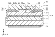
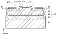
- FIG. 2 is a schematic cross-sectional view showing the overall configuration of the semiconductor laser device according to Embodiment 1.
- FIG. 3 is an enlarged view of the inside of the dashed frame shown in FIG. 2.
- FIG. 4 is a schematic cross-sectional view showing the structure of an insulating film near the facet of the semiconductor laser device according to the first embodiment.
- FIG. 5 is a cross-sectional view showing the configuration of a semiconductor laser device of a comparative example.
- FIG. 6 is a graph showing the relationship between the threshold current and the length from the end of the upper surface of the ridge to the opening of the semiconductor laser device according to the first embodiment.
- FIG. 7 is a schematic cross-sectional view showing the first step of the method for manufacturing the semiconductor laser device according to Embodiment 1.
- FIG. 8 is a schematic cross-sectional view showing the second step of the method for manufacturing the semiconductor laser device according to Embodiment 1.
- FIG. 9 is a schematic cross-sectional view showing the third step of the method for manufacturing the semiconductor laser device according to the first embodiment.
- 10 is a schematic cross-sectional view showing the fourth step of the method for manufacturing the semiconductor laser device according to Embodiment 1.
- FIG. 11 is a schematic cross-sectional view showing the fifth step of the method for manufacturing the semiconductor laser device according to Embodiment 1.
- FIG. 12 is a schematic cross-sectional view showing the sixth step of the method for manufacturing the semiconductor laser device according to Embodiment 1.
- FIG. 13 is a schematic cross-sectional view showing the seventh step of the method for manufacturing the semiconductor laser device according to Embodiment 1.
- FIG. 14 is a schematic cross-sectional view showing the eighth step of the method for manufacturing the semiconductor laser device according to Embodiment 1.
- FIG. 15 is a schematic cross-sectional view showing the ninth step of the method for manufacturing the semiconductor laser device according to Embodiment 1.
- FIG. 16 is a schematic cross-sectional view showing the tenth step of the method for manufacturing the semiconductor laser device according to Embodiment 1.
- FIG. 17 is a schematic cross-sectional view showing the eleventh step of the method for manufacturing the semiconductor laser device according to Embodiment 1.
- FIG. 18 is a schematic cross-sectional view showing the twelfth step of the method for manufacturing the semiconductor laser device according to Embodiment 1.
- FIG. 19A and 19B are diagrams for explaining a first step of forming an opening in an insulating film according to Embodiment 1.
- FIG. 20A and 20B are diagrams for explaining the second step of forming the opening of the insulating film according to the first embodiment.
- 21A and 21B are diagrams for explaining the third step of forming the opening of the insulating film according to the first embodiment.
- FIG. 22 is an example of a SEM image of a cross section of the semiconductor laser device according to Embodiment 1 in a direction perpendicular to the laser beam.
- FIG. 23 is a schematic plan view showing the overall configuration of a semiconductor laser device according to Embodiment 2.
- FIG. FIG. 24 is a schematic cross-sectional view showing the overall configuration of a semiconductor laser device according to Embodiment 2.
- FIG. 25 is an enlarged view of the inside of the dashed frame shown in FIG. 24.
- FIG. 26 is a schematic cross-sectional view showing the configuration of the Cr layer near the facet of the semiconductor laser device according to the second embodiment.
- FIG. 27 is a schematic plan view showing the overall configuration of a semiconductor laser device according to Embodiment 3.
- FIG. FIG. 28 is a schematic cross-sectional view showing the overall configuration of a semiconductor laser device according to Embodiment 3.
- FIG. 29 is an enlarged view of the inside of the dashed frame shown in FIG.
- FIG. FIG. 30 is a schematic cross-sectional view showing the structure of the contact electrode near the facet of the semiconductor laser device according to the third embodiment.
- FIG. 31 is a schematic plan view showing the overall configuration of a semiconductor laser device according to Embodiment 4.
- FIG. 32 is a schematic cross-sectional view showing the overall configuration of a semiconductor laser device according to Embodiment 4.
- FIG. 33 is an enlarged view of the inside of the dashed frame shown in FIG. 32.
- FIG. FIG. 34 is a schematic cross-sectional view showing the structure of the contact electrode near the facet of the semiconductor laser device according to the fourth embodiment.
- 35 is a schematic plan view showing the overall configuration of a semiconductor laser device according to Embodiment 5.
- FIG. 36 is a schematic cross-sectional view showing the overall configuration of a semiconductor laser device according to Embodiment 5.
- FIG. 37 is an enlarged view of the inside of the dashed frame shown in FIG. 36.
- FIG. FIG. 38 is a schematic cross-sectional view showing the structure of the contact electrode near the facet of the semiconductor laser device according to the fifth embodiment.
- FIG. 39 is a schematic plan view showing the overall configuration of a semiconductor laser device according to Embodiment 6.
- FIG. FIG. 40 is a schematic cross-sectional view showing the overall configuration of a semiconductor laser device according to Embodiment 6.
- FIG. FIG. 41 is a schematic cross-sectional view showing a cross section of a side surface located on the periphery of the opening of the insulating film according to Modification 1.
- FIG. 42 is a schematic cross-sectional view showing a cross-section of a side surface positioned on the periphery of the opening of the insulating film according to Modification 2.
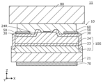
- FIG. 43 is a schematic cross-sectional view showing the overall configuration of a semiconductor laser device using the semiconductor laser element according to Embodiment 1.
- each figure is a schematic diagram and is not necessarily strictly illustrated. Therefore, the scales and the like are not always the same in each drawing.
- symbol is attached
- the terms “upper” and “lower” do not refer to vertical upper and vertical lower in absolute spatial recognition, but are defined by relative positional relationships based on the stacking order in the stacking structure. used as a term Also, the terms “above” and “below” are used not only when two components are spaced apart from each other and there is another component between the two components, but also when two components are spaced apart from each other. It also applies when they are arranged in contact with each other.
- Embodiment 1 A semiconductor laser device and a manufacturing method thereof according to Embodiment 1 will be described.
- FIG. 1 and 2 are a schematic plan view and a cross-sectional view, respectively, showing the overall configuration of a semiconductor laser device 10 according to this embodiment.
- FIG. 2 shows a cross section of the semiconductor laser device 10 taken along line II-II of FIG.
- Each figure shows an X-axis, a Y-axis, and a Z-axis that are orthogonal to each other.
- the X, Y, and Z axes are a right-handed Cartesian coordinate system.
- the stacking direction of the semiconductor laser element 10 is parallel to the Z-axis direction, and the main emission direction of light (laser light in this embodiment) is parallel to the Y-axis direction.
- the semiconductor laser element 10 includes a semiconductor laminate 10S, and a laser beam is emitted from an end face 10F (see FIG. 1) perpendicular to the lamination direction (that is, the Z-axis direction) of the semiconductor laminate 10S. is emitted.
- the semiconductor laser device 10 is a nitride semiconductor laser device having two facets 10F and 10R forming a resonator, as shown in FIG.
- the end surface 10F is a front end surface that emits laser light
- the end surface 10R is a rear end surface having a higher reflectance than the end surface 10F.
- the reflectances of the end faces 10F and 10R are 6% and 98%, respectively.
- the semiconductor laser element 10 also has a waveguide formed between the facet 10F and the facet 10R.
- the cavity length of the semiconductor laser device 10 according to the present embodiment (that is, the distance between the facets 10F and 10R) is approximately 1000 ⁇ m.
- the semiconductor laser element 10 emits blue-violet light having a peak wavelength in the 405 nm band, for example.
- the semiconductor laser element 10 includes a substrate 21, a semiconductor laminate 10S, an insulating film 30, a contact electrode 40, an adhesion assisting layer 50, a pad electrode 60, and an N-side electrode . Prepare.
- the substrate 21 is a plate-like member that serves as a base for the semiconductor laser element 10 .
- substrate 21 is an N-type GaN substrate.
- the semiconductor laminate 10S is a laminate containing a nitride semiconductor.
- the semiconductor laminate 10S has a plurality of semiconductor layers laminated in the lamination direction.
- the semiconductor stack 10S has an N-side semiconductor layer 22, an active layer 23, and a P-side semiconductor layer 24. As shown in FIG.
- the N-side semiconductor layer 22 is an example of a first conductivity type first semiconductor layer arranged above the substrate 21 and below the active layer 23 .
- the N-side semiconductor layer 22 contains a nitride semiconductor.
- the N-side semiconductor layer 22 includes an N-type clad layer having a lower refractive index than the active layer 23 .
- the N-side semiconductor layer 22 is, for example, an N-type AlGaN layer. Note that the N-side semiconductor layer 22 may include layers other than the N-type clad layer.
- the N-side semiconductor layer 22 may include, for example, a buffer layer, an optical guide layer, and the like.
- the active layer 23 is a light-emitting layer arranged above the N-side semiconductor layer 22 .
- active layer 23 contains a nitride semiconductor and has a quantum well structure.
- the active layer 23 may have a single quantum well or multiple quantum wells.
- the active layer 23 has a plurality of barrier layers made of InGaN and a plurality of well layers made of InGaN.
- the P-side semiconductor layer 24 is an example of a second semiconductor layer of a second conductivity type different from the first conductivity type, which is arranged above the active layer 23 .
- the P-side semiconductor layer 24 contains a nitride semiconductor.
- the P-side semiconductor layer 24 includes a P-type cladding layer having a lower refractive index than the active layer 23 .
- the P-side semiconductor layer 24 is, for example, a P-type AlGaN layer.
- the P-side semiconductor layer 24 may include layers other than the P-type clad layer.
- the P-side semiconductor layer 24 may include, for example, an optical guide layer, an electron barrier layer, a contact layer, and the like. Also, the P-side semiconductor layer 24 may have a superlattice structure.
- the P-side semiconductor layer 24 has a ridge 24R extending in the laser light emitting direction.
- the ridge 24R is a portion of the P-side semiconductor layer 24 that protrudes in the Z-axis direction.
- the P-side semiconductor layer 24 may be formed with two grooves arranged along the ridge 24R and extending in the Y-axis direction.
- the ridge width (that is, the dimension of the ridge 24R in the X-axis direction) is approximately 7 ⁇ m.
- a dotted line indicating the ridge 24R in FIG. 1 corresponds to the position of the X-axis direction end of the upper surface 24Rt of the ridge 24R (not visible from the upper surface of the semiconductor laser element 10).
- the insulating film 30 is a layer arranged above the P-side semiconductor layer 24 (that is, the second semiconductor layer).
- the insulating film 30 is a layer that is arranged between the semiconductor stacked body 10S and the pad electrode 60 and has electrical insulation.
- the insulating film 30 has an opening 30a arranged at a position corresponding to the upper surface 24Rt of the ridge 24R.
- the insulating film 30 is arranged in a region of the upper surface of the P-side semiconductor layer 24 other than the central portion of the upper surface 24Rt of the ridge 24R.
- FIG. 3 is an enlarged view of the inside of the dashed frame III shown in FIG. 2.
- FIG. FIG. 4 is a schematic cross-sectional view showing the configuration of the insulating film 30 near the end surface 10R of the semiconductor laser device 10 according to this embodiment.
- FIG. 4 shows a part of the cross section near the opening 30a of the insulating film 30 along line IV-IV in FIG.
- the side surface 30s of the insulating film 30 located at the periphery of the opening 30a is divided into a lower side surface region 31 and an upper side surface region 32 disposed above the lower side surface region 31. have.
- the lower side surface region 31 and the upper side surface region 32 have different angles of inclination with respect to the upper surface 24Rt of the ridge.
- the dimension (film thickness) in the stacking direction of the lower side surface region 31 is, for example, 100 nm or more and 150 nm or less.
- the dimension of the upper side surface region 32 in the direction perpendicular to the stacking direction is, for example, 100 nm or more and 150 nm or less.
- the thickness of the insulating film 30 arranged on the upper surface 24Rt of the ridge 24R is 300 nm.
- the thickness of the insulating film 30 arranged on the upper surface 24Rt of the ridge 24R should be 150 nm or more.
- the thickness of the insulating film 30 disposed on the upper surface 24Rt of the ridge 24R is too thick, cracks or peeling may occur due to the difference in thermal expansion coefficient from the semiconductor layer.
- the thickness of the insulating film 30 may be 450 nm or less.
- the length from the end of the top surface 24Rt of the ridge 24R to the opening 30a (the length a2 shown in FIG. 3) of the insulating film 30 arranged on the top surface 24Rt of the ridge 24R is 300 nm. .
- the insulating film 30 and the contact electrode 40 are separated.
- the distance in the X-axis direction (distance a1 shown in FIG. 3) and the distance in the Y-axis direction (distance a5 shown in FIG. 4) between the insulating film 30 and the contact electrode 40 are All are 250 nm or more and 300 nm or less.
- the material for forming the insulating film 30 is not particularly limited as long as it is an insulating material.
- the insulating film 30 is made of silicon oxide. A detailed configuration and effect of the insulating film 30 will be described later.
- the contact electrode 40 is an electrode arranged above the P-side semiconductor layer 24 and in contact with the P-side semiconductor layer 24 .
- the contact electrode 40 faces the P-side semiconductor layer 24 above the P-side semiconductor layer 24 and is in contact with the P-side semiconductor layer 24 .
- the contact electrode 40 is arranged in the opening 30 a of the insulating film 30 .
- the contact electrode 40 may contain Pd or ITO.
- the contact electrode 40 is, for example, a single layer film or a multilayer film formed of at least one of Ag, Ni, Pd, Cr, and Pt, or indium tin oxide (ITO), indium zinc oxide (IZO), It may be made of conductive metal oxide such as zinc oxide (ZnO) or InGaZnO x (IGZO).
- the contact electrode 40 has a Pd layer with a thickness of 40 nm in contact with the P-side semiconductor layer 24 and a Pt layer with a thickness of 35 nm disposed above the Pd layer.
- the Pt layer has a function of suppressing migration of metal elements from the pad electrode 60 to the Pd layer.
- the adhesion auxiliary layer 50 is a layer arranged above the insulating film 30 .
- the adhesion auxiliary layer 50 is arranged between the insulating film 30 and the pad electrode 60 and has a function of enhancing adhesion between the pad electrode 60 and the insulating film 30 .
- the adhesion assisting layer 50 has openings 50 a (or slits) at positions corresponding to the openings 30 a of the insulating film 30 .
- the opening 30a of the insulating film 30 is arranged inside the opening 50a of the adhesion auxiliary layer 50 when the substrate 21 is viewed from above.
- the adhesion auxiliary layer 50 may contain Ti or Cr.
- the adhesion assisting layer 50 contains Ti and the insulating film 30 is an oxide, the adhesion between the adhesion assisting layer 50 and the insulating film 30 can be further enhanced. This is because when the insulating film 30 is an oxide, the adhesion assisting layer 50 made of a metal film is also made of a material that easily forms an oxide, so that they are strongly bonded. In the present embodiment, the adhesion assisting layer 50 has a laminated structure including a 10 nm-thickness Ti film in contact with the insulating film 30 and a 50 nm-thickness Pt film disposed on the Ti film.
- the adhesion auxiliary layer 50 and the contact electrode 40 are separated from each other.
- the distance in the X-axis direction (distance a3 shown in FIG. 3) from the peripheral edge of the opening 50a of the adhesion auxiliary layer 50 to the upper surface 24Rt of the ridge 24R is 1000 nm.
- the pad electrode 60 is a conductive layer arranged above the insulating film 30 and the contact electrode 40 and in contact with the contact electrode 40 .
- Pad electrode 60 contains Au.
- the pad electrode 60 is an Au layer with a thickness of approximately 1.6 ⁇ m.
- the N-side electrode 70 is a conductive layer arranged on the lower surface of the substrate 21 (that is, the main surface of the substrate 21 opposite to the main surface on which the semiconductor laminate 10S is arranged).
- the N-side electrode 70 may contain Pd or ITO. Thereby, the contact resistance between the N-side electrode 70 and the substrate 21 can be reduced, so that the operating voltage of the semiconductor laser device 10 can be reduced.
- the N-side electrode 70 may be, for example, a single layer film or a multilayer film formed of at least one of Cr, Ti, Ni, Pd and Pt.
- the N-side electrode 70 has a Ti layer with a thickness of 10 nm in contact with the substrate 21, a Pt layer with a thickness of 35 nm in contact with the Ti layer, and an Au layer with a thickness of 300 nm in contact with the Pt layer.
- FIG. 5 is a cross-sectional view showing the configuration of a semiconductor laser device of a comparative example.
- FIG. 5 shows a cross section near the end of the upper surface 24Rt of the ridge 24R of the semiconductor laser device of the comparative example, which is taken in a direction perpendicular to the laser light emission direction.
- the semiconductor laser device of the comparative example includes a P-side semiconductor layer 24, a contact electrode 40, an insulating film 930, an adhesion auxiliary layer 50, and a pad electrode 60, similarly to the semiconductor laser device 10 according to the present embodiment.
- the semiconductor laser device of the comparative example differs from the semiconductor laser device 10 in the structure of the insulating film 930, but is the same in other structures.
- the insulating film 930 has an opening 930a like the insulating film 30 .
- the opening 930a is formed by wet etching.
- a side surface located at the periphery of the opening of the insulating film 30 has a single side area 931 with a uniform inclination angle with respect to the upper surface 24Rt of the ridge 24R.
- the side area 931 of the insulating film 930 is inclined relatively greatly.
- the thickness of the insulating film 930 at the peripheral portion of the opening 930a becomes thinner as it approaches the opening 930a. Therefore, if the opening 930a of the insulating film 930 is enlarged too much, the thickness on the end of the insulating film 930 located on the upper surface 24Rt of the ridge 24R becomes thin. As a result, electrical insulation between the upper surface 24Rt of the ridge 24R and the pad electrode 60 may not be maintained.
- the opening of the insulating film 930 from the end of the top surface 24Rt of the ridge 24R is required. It is necessary to increase the length to the portion 930a (length a2 in FIG. 5). As a result, the area of the opening 930a (area in top view) is reduced, so the area of the contact electrode 40 needs to be reduced. Since the area of the current injection region is accordingly reduced, the operating voltage of the semiconductor laser device is increased.
- the side surface 30s located at the periphery of the opening 30a of the insulating film 30 of the semiconductor laser device 10 includes the lower side surface region 31 and the upper side surface located above the lower side surface region 31. region 32;
- the lower side surface region 31 and the upper side surface region 32 have different angles of inclination with respect to the upper surface 24Rt of the ridge 24R.
- the width of the inclined region can be reduced as compared with the case where the side surface 30s of the insulating film 30 is composed only of a region with a small inclination angle like the side surface of the insulating film 930 of the comparative example.
- the area of the opening 30a can be increased while ensuring the thickness of the end portion of the insulating film 30 located on the upper surface 24Rt of the ridge 24R of the insulating film 30.
- the area of the contact electrode 40 can be increased. Accordingly, since the area of the current injection region can be increased, the operating voltage of the semiconductor laser device 10 can be reduced.
- the inclination angle (angle ⁇ 1 shown in FIG. 3) of the lower side surface region 31 with respect to the top surface 24Rt of the ridge 24R is the same as the inclination angle (angle ⁇ 1 shown in FIG. 3) of the upper side surface region 32 with respect to the top surface 24Rt of the ridge 24R. is larger than the angle ⁇ 2).
- the width of the lower side surface region 31 having a small film thickness and a low insulation resistance can be reduced, so that the insulating property of the insulating film 30 can be further enhanced.
- the inclination angle of the ridge 24R of the upper side surface region 32 with respect to the upper surface 24Rt may be less than 90 degrees.
- the risk of cracks occurring in the adhesion-assisting layer 50 on the corners of the insulating film 30 can be reduced.
- the inclination angle of the upper side surface region 32 may be 40 degrees or more and 60 degrees or less. In this case, both the increase in the contact area due to the inclination and the avoidance of cracking at the corners can be achieved, and the effect is greatest at 45 degrees.
- the contact area between the pad electrode 60 and the upper end portion of the insulating film 30 located on the upper surface 24Rt of the ridge 24R can be increased. Therefore, the adhesion between the insulating film 30 and the pad electrode 60 can be enhanced.
- the inclination angle of the ridge 24R of the lower side surface region 31 with respect to the upper surface 24Rt may be 90 degrees or less.
- the risk of voids occurring between the insulating film 30 and the adhesion assisting layer 50 can be reduced.
- the inclination angle of the lower side surface region 31 may be 65 degrees or more and 85 degrees or less. In this case, it was possible to achieve both an increase in the contact area due to the inclination and the avoidance of void generation, and the effect was the greatest at 75 degrees.
- the area of the opening 30a of the insulating film 30 can be increased. Therefore, since the area of the current injection region can be increased, the operating voltage of the semiconductor laser device 10 can be further reduced.
- the insulating film 30 is arranged on both ends of the upper surface 24Rt of the ridge 24R in the cross section perpendicular to the laser light emitting direction of the semiconductor laser device 10 (see FIGS. 1 and 2). .
- the insulating film 30 may cover the entire periphery of the ridge 24R when viewed from above. Thereby, the current flowing near the side surface of the ridge 24R can be further reduced.
- the side surface of the ridge 24R located at the end in the width direction of the ridge 24R (that is, the X-axis direction in each drawing) is the P-side semiconductor layer 24. It has a tapered shape that is inclined with respect to the stacking direction.
- the upper surface of the insulating film 30 arranged on the side surface of the ridge 24R is inclined with respect to the stacking direction. Since the side surfaces of the ridge 24R are inclined with respect to the stacking direction in this way, it is easier to stack the insulating film 30 along the side surfaces of the ridge 24R than when the side surfaces of the ridge 24R are parallel to the stacking direction. Become.
- the insulating film 30 By stacking the insulating film 30 on the side surface of the ridge 24R, it is possible to secure a refractive index difference between the ridge 24R and the external region in the width direction of the ridge 24R. Therefore, light can be confined in the ridge 24R and the area below it. Note that the thickness of the region of the insulating film 30 located on the side surface of the ridge 24R (thickness in the direction perpendicular to the side surface) is smaller than the maximum thickness of the insulating film 30 located on the upper surface 24Rt of the ridge 24R. good too.
- the insulating film 30 and the contact electrode 40 may be separated from each other.
- hydrogen atoms contained in the insulating film 30 can move to the contact electrode 40 .
- hydrogen atoms are occluded in the Pd layer included in the contact electrode 40, which can increase the electric resistance of the Pd layer.
- the insulating film 30 and the contact electrode 40 are spaced apart from each other, it is possible to suppress the movement of elements from the insulating film 30 to the contact electrode 40 , so that the electrical resistance of the contact electrode 40 increases. can be suppressed.
- the distance between insulating film 30 and contact electrode 40 (distance a1 shown in FIG. 3) is 250 nm or more and 300 nm or less. Thereby, it is possible to prevent the area of the contact electrode 40 from being reduced while separating the insulating film 30 and the contact electrode 40 .
- FIG. 6 is a graph showing the relationship between the threshold current and the length (a2) from the end of the top surface 24Rt of the ridge 24R of the semiconductor laser device 10 according to the present embodiment to the opening 30a.
- the relationship shown in FIG. 6 was determined by experiment. As shown in FIG. 6, the threshold current has a minimum value when the length a2 is 750 nm, and especially when the length a2 is less than 100 nm, the threshold current sharply increases.
- the cause of this phenomenon is presumed as follows. As the length a2 becomes smaller, the current flowing from the pad electrode 60 to the vicinity of the side surface of the ridge 24R through the insulating film 30 increases. Along with this, the light density near the side surface of the ridge 24R increases, and the light amplification gain decreases due to the hole burning phenomenon caused by the increased light density. Therefore, it is presumed that the threshold current increases when the length a2 is less than 100 nm. Also, the length a2 may be 750 nm or less. As a result, it is possible to prevent the width of the opening 30a from becoming too small with respect to lateral light confinement. Therefore, in this embodiment, the length a2 may be 100 nm or more and 750 nm or less.
- the inclination start position of the peripheral side surface 30 s of the opening 30 a of the insulating film 30 is the upper end of the upper side surface region 32 . Since the thickness of the insulating film 30 becomes thinner as it approaches the opening 30a from this tilt start position, the tilt start position may be above the upper surface 24Rt of the ridge 24R. As a result, it is possible to prevent the thickness of the insulating film 30 located on the upper surface 24Rt of the ridge 24R from becoming thin on the ridge end portion.
- the distance in the X-axis direction (distance a4 shown in FIG. 3) from the tilt start position located above the upper surface 24Rt of the ridge 24R to the end of the upper surface 24Rt of the ridge 24R is 130 nm or more and 180 nm or less. is.
- FIG. 7 to 18 are schematic cross-sectional views showing each step of the method of manufacturing the semiconductor laser device 10 according to this embodiment. 7-18 show cross-sections similar to FIG.
- an N-side semiconductor layer 22 is formed as a first conductivity type first semiconductor layer above a substrate 21, an active layer 23 is formed above the N-side semiconductor layer 22, A P-side semiconductor layer 24 is formed as a second semiconductor layer above the active layer 23 .
- the substrate 21 is prepared.
- a wafer (GaN substrate) made of N-type GaN is prepared as the substrate 21 .
- an N-side semiconductor layer 22, an active layer 23, and a P-side semiconductor layer 24 are laminated in order on the substrate 21 by an epitaxial growth technique based on the MOCVD (Metal Organic Chemical Vapor Deposition) method. Thereby, the semiconductor stacked body 10S can be formed.
- MOCVD Metal Organic Chemical Vapor Deposition
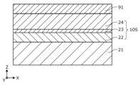
- an insulating film 91 is formed above the P-side semiconductor layer 24, and the semiconductor laminate 10S is annealed. More specifically, as the insulating film 91, a silicon oxide film is formed using an atmospheric pressure CVD (Chemical Vapor Deposition) method or the like. In this embodiment, the thickness of insulating film 91 is 200 nm. Annealing is then performed to remove at least some of the hydrogen atoms contained in the semiconductor stacked body 10S. A low pressure CVD method may be used to form the silicon oxide film.
- CVD Chemical Vapor Deposition
- an insulating film 92 is formed above the insulating film 91, as shown in FIG. Specifically, as the insulating film 92, a silicon oxide film is formed using an atmospheric pressure CVD method or the like. In this embodiment, the thickness of the insulating film 92 is 300 nm. Low-pressure CVD may be used to form the silicon oxide film.
- element isolation grooves 10D are formed for separating the semiconductor laser elements 10 into individual pieces.
- the device isolation grooves 10D are formed at positions corresponding to both ends of the semiconductor laser device 10 in the X-axis direction.
- the element isolation trench 10D reaches the inside of the N-side semiconductor layer 22 from the upper surface of the semiconductor stacked body 10S.
- a method for forming the isolation trench 10D is not particularly limited.
- the element isolation trench 10D may be formed using, for example, a photolithography technique and etching, or may be formed by laser processing.
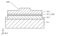
- a ridge 24R is formed in the P-side semiconductor layer 24 as shown in FIG.
- the method of forming the ridge 24R is not particularly limited.
- the ridge 24R is formed using photolithography and etching, for example.
- the insulating films 91 and 92 are patterned, and the patterned insulating films 91 and 92 are used as masks to partially etch the P-side semiconductor layer 24 to form the ridge 24R.
- the insulating film 91 and the insulating film 92 are arranged above the ridge 24R in FIG. 10, part of the insulating film 91 and the insulating film 92 can be removed during etching.
- the insulating films 91 and 92 are removed. Specifically, the insulating film 91 and the insulating film 92 are removed using wet etching.
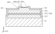
- an insulating film 30 is formed above the P-side semiconductor layer 24, as shown in FIG.
- a silicon oxide film is formed as the insulating film 30 using a low pressure CVD method or the like.
- An atmospheric pressure CVD method may be used to form the silicon oxide film.
- FIG. 19 to 21 are diagrams for explaining each step of forming the opening 30a of the insulating film 30 according to this embodiment.
- 19 to 21 show schematic cross-sectional views in each step of the ridge 24R and the insulating film 30 arranged thereabove.
- a resist 95 is formed in a region of the insulating film 30 other than the region corresponding to the opening 30a.
- the region corresponding to the opening 30a in the insulating film 30 is etched by the first etching method by the first film thickness (first etching step).
- the first etching method is dry etching. Specifically, a region of the insulating film 30 not covered with the resist is etched using dry etching.
- the first film thickness is, for example, 150 nm.
- a dry etching method for example, an ICP (Inductively Coupled Plasma) method with a frequency of 13.56 MHz can be used.
- the top power is 120 W
- the bias power is 40 W
- the gas pressure is 1 Pa
- the gas type is CHF 3 (flow rate 35 sccm).
- the region corresponding to the opening 30a in the insulating film 30 is etched by a second film thickness by a second etching method different from the first etching method (second etching method).
- second etching method is wet etching. Specifically, a region of the insulating film 30 not covered with the resist is etched using wet etching.
- the second film thickness is, for example, 150 nm.
- a wet etching method for example, a dip processing method using BHF (buffered hydrofluoric acid) can be used. After the wet etching process, the element including the processed semiconductor stack 10S is washed with pure water and then spin-dried.
- the insulating film 30 having the lower side surface region 31 and the upper side surface region 32 can be formed on the side surface 30s located at the periphery of the opening 30a.
- the contact electrode 40 is formed in the opening 30a of the insulating film 30 so as to be in contact with the P-side semiconductor layer 24. Then, as shown in FIG. In this embodiment, a Pd layer and a Pt layer are formed as the contact electrode 40 .
- the contact electrode 40 is formed only on the region inside the opening 30a of the upper surface 24Rt of the ridge 24R using, for example, photolithography and vapor deposition.
- an adhesion auxiliary layer 50 having openings 50a is formed.
- the adhesion assisting layer 50 made of a Ti film and a Pt film is formed on the insulating film 30 using photolithography and vapor deposition.
- pad electrodes 60 are formed. Specifically, an Au film is formed above the contact electrode 40 and the insulating film 30 by photolithography and vapor deposition. A plating method may be used to form the pad electrodes.
- the thickness of the substrate 21 is reduced by polishing and etching the lower surface of the substrate 21 .
- an N-side electrode 70 is formed on the lower surface of the substrate 21.
- the N-side electrode 70 is formed by sequentially forming a Ti film, a Pt film, and an Au film using photolithography and vapor deposition.
- the semiconductor laser device 10 according to the present embodiment can be manufactured by the manufacturing method as described above.
- FIG. 22 shows a configuration example of the semiconductor laser device 10 manufactured by the manufacturing method described above.
- FIG. 22 is an example of a SEM image of a cross section of the semiconductor laser device 10 according to this embodiment in a direction perpendicular to the laser beam.
- the insulating film 30 having the lower side surface region 31 and the upper side surface region 32 on the side surface 30s located at the periphery of the opening 30a can be formed by the manufacturing method described above.
- the present embodiment by using dry etching as the first etching method, it is possible to easily etch to a desired film thickness. Moreover, by using wet etching as the second etching method, etching of the P-side semiconductor layer 24 in the second etching process can be reduced. Therefore, damage to the upper surface 24Rt of the ridge 24R can be reduced, and defects formed on the upper surface 24Rt can be suppressed, thereby improving flatness.
- first film thickness and the second film thickness are equal in the above embodiment, the first film thickness and the second film thickness may be different. Also, the first film thickness may be thicker than the second film thickness. For example, if the first etching step is dry etching, the first film thickness can be increased and the inclination angle of the upper side surface region 32 can be increased by changing conditions such as the etching gas. By making the first film thickness thicker than the second film thickness, the area of the opening 30a can be further enlarged.
- the first etching method and the second etching method which are different from each other, may be wet etching or dry etching, for example. Some processing conditions such as an etchant may be different between the first etching method and the second etching method.
- Embodiment 2 A semiconductor laser device according to Embodiment 2 will be described.
- the semiconductor laser device according to the present embodiment is similar to the semiconductor laser device according to the first embodiment in that it includes a Cr layer instead of the Ti film and the Pt film as the adhesion assisting layer, and that the contact electrode is a Pd layer. It differs from the semiconductor laser device 10 .
- the semiconductor laser device according to the present embodiment will be described below with reference to FIGS. 23 to 26, focusing on differences from the semiconductor laser device 10 according to the first embodiment.
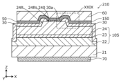
- FIG. 23 and 24 are a schematic plan view and a cross-sectional view, respectively, showing the overall configuration of the semiconductor laser device 110 according to this embodiment.
- FIG. 24 shows a cross section of the semiconductor laser device 110 along line XXIV-XXIV in FIG. 25 is an enlarged view of the inside of the dashed frame XXV shown in FIG. 24.
- FIG. FIG. 26 is a schematic cross-sectional view showing the configuration of the Cr layer 150 near the facet 10R of the semiconductor laser device 110 according to this embodiment.
- FIG. 26 shows a portion of the cross section of the Cr layer 150, etc. taken along line XXVI-XXVI of FIG.
- the semiconductor laser element 110 includes a substrate 21, a semiconductor laminate 10S, an insulating film 30, a contact electrode 140, a Cr layer 150, a pad electrode 60, and an N-side electrode . Prepare.
- the contact electrode 140 according to the present embodiment is different from the contact electrode 40 according to Embodiment 1 in that it is a Pd layer with a film thickness of 40 nm, but is identical in other respects. As described above, the contact electrode 140 according to this embodiment does not have a layer that suppresses migration of the metal element to the Pd layer.
- the Cr layer 150 is arranged between the insulating film 30 and the contact electrode 140 and the pad electrode 60 .
- the Cr layer 150 covers the entire bottom surface of the pad electrode 60, as shown in FIGS.
- the side surfaces of the pad electrode 60 are flush with the side surfaces of the Cr layer 150, but they do not have to be flush.
- the Cr layer 150 has a function of suppressing peeling of the pad electrode 60 and a function of suppressing movement of the metal element from the pad electrode 60 to the contact electrode 140 . For example, when the pad electrode 60 is joined with solder containing Sn, the Sn element may migrate to the Pd layer included in the contact electrode 140 via the pad electrode 60 .
- the movement of the Sn element to the Pd layer can increase the electrical resistance of the Pd layer.
- the Cr layer between the contact electrode 140 and the pad electrode 60 , it is possible to suppress migration of metal elements such as Sn from the pad electrode 60 to the contact electrode 140 . Therefore, an increase in electrical resistance of contact electrode 140 can be suppressed.
- the film thickness of the Cr layer 150 is not particularly limited, it is 100 nm in this embodiment.
- the Cr layer and the pad electrode are formed by one photolithographic technique for two deposition methods. 1, but otherwise uses a similar process. If the same manufacturing method continues like this, photolithography can be partially omitted.
- Embodiment 3 A semiconductor laser device according to Embodiment 3 will be described.
- the semiconductor laser device according to this embodiment differs from the semiconductor laser device 110 according to the second embodiment in the structure of the contact electrodes.
- the semiconductor laser device according to the present embodiment will be described below with reference to FIGS. 27 to 30, focusing on differences from the semiconductor laser device 110 according to the second embodiment.
- FIG. 27 and 28 are a schematic plan view and a cross-sectional view, respectively, showing the overall configuration of a semiconductor laser device 210 according to this embodiment.
- FIG. 28 shows a cross section of the semiconductor laser device 210 taken along line XXVIII--XXVIII of FIG. 29 is an enlarged view of the inside of the dashed frame XXIX shown in FIG. 28.
- FIG. FIG. 30 is a schematic cross-sectional view showing the configuration of the contact electrode 240 near the end face 10R of the semiconductor laser device 210 according to this embodiment.
- FIG. 30 shows a part of the cross section near the insulating film 30 of the contact electrode 240 along line XXX-XXX in FIG.
- a semiconductor laser element 210 includes a substrate 21, a semiconductor laminate 10S, an insulating film 30, a contact electrode 240, a Cr layer 150, a pad electrode 60, and an N-side electrode . Prepare.
- the contact electrode 240 according to the present embodiment is a Pd layer with a thickness of 40 nm, but faces the insulating film 30 as shown in FIGS.
- the contact electrode 140 differs from the contact electrode 140 according to the second embodiment in that the side surface 240 s that faces the contact electrode is inclined with respect to the stacking direction of the P-side semiconductor layer 24 .
- the contact electrode 140 when the side surfaces are parallel to the stacking direction, it is difficult for Cr to be stacked on the side surfaces. For this reason, slit-like voids may occur in the Cr layer 150 , starting from near the upper ends of the side surfaces of the contact electrodes 140 .
- the contact electrode 240 since the side surface 240s is inclined with respect to the lamination direction, Cr is easily laminated on the side surface 240s. Therefore, the occurrence of slit-shaped voids in the Cr layer 150 can be suppressed.
- the inclination angle of the side surface 240s of the contact electrode 240 with respect to the upper surface 24Rt of the ridge 24R may be, for example, 15 degrees or less. Thereby, the formation of voids in the Cr layer 150 can be suppressed more reliably.
- the contact electrode 240 according to this embodiment can be easily formed by using, for example, planetary vapor deposition.
- the Cr layer 150 is arranged between the contact electrode 240 and the pad electrode 60, so that Sn It is possible to suppress the movement of metal elements such as ions from the pad electrode 60 to the contact electrode 240 . Therefore, an increase in electrical resistance of contact electrode 240 can be suppressed.
- the Cr layer 150 is laminated on the contact electrode 240 . More specifically, Cr layer 150 covers contact electrode 240 . That is, the Cr layer 150 covers the entire side surfaces 240 s and the top surface of the contact electrode 240 . As a result, metal elements such as Sn can be prevented from moving from the pad electrode 60 to the entire contact electrode 240 .
- the Cr layer 150 and the like according to the present embodiment have a characteristic configuration as described below.
- the Cr layer 150 has a region sandwiched between the insulating film 30 and the contact electrode 240 and sandwiched between the P-side semiconductor layer 24 and the pad electrode 60 .
- the Cr layer 150 contacts the P-side semiconductor layer 24 on the lower surface of the region between the insulating film 30 and the contact electrode 240 and contacts the pad electrode 60 on the upper surface.
- the Cr layer 150 has a concave portion on the upper surface located above the region located between the insulating film 30 and the contact electrode 240 .
- the Cr layer 150 is arranged along the side surface 30 s located at the periphery of the opening 30 a of the insulating film 30 . Therefore, the Cr layer 150 has a two-stage inclined surface composed of an inclined surface facing the lower side surface region 31 of the insulating film 30 and an inclined surface facing the upper side surface region 32 of the insulating film 30 . Along with this, the upper surface of the region of the Cr layer 150 that is located on the insulating film 30 also has a two-stage inclined surface. Thereby, the adhesion between the upper surface of the Cr layer 150 and the pad electrode 60 laminated on the upper surface can be enhanced.
- the top surface of the Cr layer 150 located on the insulating film 30 located on the ridge 24R is above the top surface of the Cr layer 150 located on the contact electrode 240.
- the upper surface of the contact electrode 240 is located below the upper surface of the insulating film 30 on the ridge 24R.
- Embodiment 4 A semiconductor laser device according to Embodiment 4 will be described.
- the semiconductor laser device according to this embodiment differs from the semiconductor laser device 110 according to the second embodiment in the structure of the contact electrodes.
- the semiconductor laser device according to the present embodiment will be described below with reference to FIGS. 31 to 34, focusing on differences from the semiconductor laser device 110 according to the second embodiment.
- FIG. 31 and 32 are a schematic plan view and a cross-sectional view, respectively, showing the overall configuration of a semiconductor laser device 310 according to this embodiment.
- FIG. 32 shows a cross section of the semiconductor laser device 310 along line XXXII-XXXII of FIG. 33 is an enlarged view of the inside of the dashed frame XXXIII shown in FIG. 32.
- FIG. 34 is a schematic cross-sectional view showing the configuration of the contact electrode 340 near the end surface 10R of the semiconductor laser device 310 according to this embodiment.
- FIG. 34 shows a part of the cross section near the insulating film 30 of the contact electrode 340 along line XXXIV-XXXIV of FIG.
- a semiconductor laser element 310 includes a substrate 21, a semiconductor laminate 10S, an insulating film 30, a contact electrode 340, a Cr layer 150, a pad electrode 60, and an N-side electrode . Prepare.
- the contact electrode 340 according to the present embodiment is a Pd layer with a film thickness of 40 nm, like the contact electrode 140 according to the second embodiment.
- the present embodiment is different from the contact electrode 140 according to the second embodiment in that the insulating film 30 covers the periphery of the contact electrode 340 (that is, the periphery of the contact electrode 340 in top view shown in FIG. 31).
- the dimension of the contact electrode 340 in the X-axis direction is equal to the dimension (that is, width) of the top surface of the ridge 24R in the X-axis direction.
- the configuration represented by the statement that the dimensions are equal includes not only the configuration in which the dimensions are exactly the same, but also the configuration in which the dimensions are substantially the same.
- a configuration represented by a statement that dimensions are equal includes a configuration with a dimensional error of 3% or less.
- the width in the X-axis direction in which the periphery of the contact electrode 340 is covered with the insulating film 30 is from the end of the upper surface 24Rt of the ridge 24R to the opening 30a of the insulating film 30 arranged on the upper surface 24Rt of the ridge 24R. (length a2 shown in FIG. 33).
- the width in the Y-axis direction (the length a6 shown in FIG. 34) of the contact electrode 340 covered with the insulating film 30 is 250 nm or more and 300 nm or less.
- the thickness of the Cr layer 150 in the vicinity of the side surfaces of the contact electrode 40 can be reduced. As a result, the above-described function of the Cr layer 150 in the vicinity of the side surfaces of the contact electrode 40 may not be sufficiently exhibited.
- the periphery including the side surface of the contact electrode 340 according to the present embodiment is covered with the insulating film 30 , it is not necessary to laminate the Cr layer 150 on the side surface of the contact electrode 340 . Therefore, it is possible to prevent the thickness of the Cr layer 150 laminated in the region in contact with the contact electrode 340 from becoming thin. As a result, the above-described functions of the Cr layer 150 are fully exhibited.
- Embodiment 5 A semiconductor laser device according to Embodiment 5 will be described.
- the semiconductor laser device according to this embodiment differs from the semiconductor laser device 10 according to the first embodiment in the structure of the contact electrodes.
- the semiconductor laser device according to the present embodiment will be described below with reference to FIGS. 35 to 38, focusing on differences from the semiconductor laser device 10 according to the first embodiment.
- FIG. 35 and 36 are a schematic plan view and a cross-sectional view, respectively, showing the overall configuration of a semiconductor laser device 410 according to this embodiment.
- FIG. 36 shows a cross section of the semiconductor laser element 410 along line XXXVI-XXXVI of FIG. 37 is an enlarged view of the inside of dashed frame XXXVII shown in FIG. 36.
- FIG. 38 is a schematic cross-sectional view showing the structure of the contact electrode 440 near the end surface 10R of the semiconductor laser device 410 according to this embodiment.
- FIG. 38 shows a part of the cross section near the insulating film 30 of the contact electrode 440 along line XXXVIII-XXXVIII of FIG.
- a semiconductor laser element 410 includes a substrate 21, a semiconductor laminate 10S, an insulating film 30, a contact electrode 440, an adhesion auxiliary layer 50, a pad electrode 60, and an N-side electrode . Prepare.
- the contact electrode 440 according to the present embodiment has a Pd layer with a thickness of 40 nm and a Pt layer with a thickness of 35 nm, like the contact electrode 40 according to the first embodiment.
- the present embodiment is different from the contact electrode 40 according to Embodiment 1 in that the insulating film 30 covers the periphery of the contact electrode 440 (that is, the periphery of the contact electrode 440 in top view shown in FIG. 35).
- the dimension of the contact electrode 440 in the X-axis direction is equal to the dimension (that is, width) of the top surface of the ridge 24R in the X-axis direction.
- the width in the X-axis direction in which the periphery of the contact electrode 440 is covered with the insulating film 30 is from the edge of the upper surface 24Rt of the ridge 24R to the opening 30a of the insulating film 30 arranged on the upper surface 24Rt of the ridge 24R. (length a2 shown in FIG. 37).
- the width in the Y-axis direction (length a6 shown in FIG. 38) of the contact electrode 440 covered with the insulating film 30 is 250 nm or more and 300 nm or less.
- the semiconductor laser element 410 having the configuration described above also has the same effect as the semiconductor laser element 10 according to the first embodiment.
- Embodiment 6 A semiconductor laser device according to Embodiment 6 will be described.
- the semiconductor laser device according to this embodiment differs from the semiconductor laser device 10 according to the first embodiment in the shape of the P-side semiconductor layer.
- the semiconductor laser device according to the present embodiment will be described below with reference to FIGS. 39 and 40, focusing on differences from the semiconductor laser device 10 according to the first embodiment.
- FIG. 40 shows a cross section of the semiconductor laser element 10A taken along line XXX--XXX in FIG.
- the semiconductor laser element 10A includes a substrate 21, a semiconductor laminate 10AS, an insulating film 30, a contact electrode 40, an adhesion auxiliary layer 50, a pad electrode 60, and an N-side electrode . Prepare.
- the semiconductor laminate 10AS has an N-side semiconductor layer 22, an active layer 23, and a P-side semiconductor layer 24A.
- the P-side semiconductor layer 24A according to this embodiment is an example of the second semiconductor layer.
- the P-side semiconductor layer 24A differs from the P-side semiconductor layer 24 according to the first embodiment in that it has protrusions 24P and grooves 24T.
- the projecting portion 24P is a portion extending along the ridge 24R.
- the position of the upper surface 24Pt of the protrusion 24P in the stacking direction is equal to the position of the upper surface 24Rt of the ridge 24R in the stacking direction.
- the P-side semiconductor layer 24A has two protrusions 24P.
- the groove 24T is a recess extending along the ridge 24R.
- the P-side semiconductor layer 24A has two trenches 24T.
- a ridge 24R is arranged between the two grooves 24T.
- Each of the two grooves 24T has a portion located between the ridge 24R and the protrusion 24P.
- the two protrusions 24P are adjacent to the ridge 24R via the groove 24T.
- each of the two grooves 24T has portions extending along the end faces 10F and 10R, as shown in FIG.
- Each of the two trenches 24T extends from the ridge 24R to the isolation trench 10D along the end faces 10F and 10R.
- the groove 24T is arranged between the projection 24P and the end faces 10F and 10R.
- the adhesion auxiliary layer 50 is arranged above the protrusion 24P.
- the adhesion auxiliary layer 50 is arranged continuously from a partial region above the groove portion 24T to a region above the protruding portion 24P.
- the semiconductor laser device 10A according to the present embodiment having the configuration described above also has the same effect as the semiconductor laser device 10 according to the first embodiment. Furthermore, in the present embodiment, since the P-side semiconductor layer 24A has the protruding portion 24P, for example, when the semiconductor laser element 10A is junction-down mounted on a mounting board or the like (that is, the semiconductor laser element 10A is mounted on the mounting board). , the stress applied to the ridge 24R can be suppressed when mounting in a state where the pad electrodes 60 face each other. That is, since the stress applied to the semiconductor stacked body 10AS during mounting can be distributed to the ridge 24R and the projecting portion 24P, it is possible to prevent the stress from concentrating on the ridge 24R. Therefore, it is possible to suppress damage to the ridge 24R during mounting.
- the angle of inclination of the lower side surface area with respect to the upper surface of the ridge is greater than the angle of inclination with respect to the upper surface of the ridge in the upper side surface area, but the invention according to the present disclosure is not limited to this.
- the angle of inclination of the lower side surface region with respect to the upper surface of the ridge may be smaller than the angle of inclination of the upper side surface region with respect to the upper surface of the ridge.
- the entire side surface 30s of the insulating film 30 located at the periphery of the opening 30a has the lower side surface area 31 and the upper side surface area 32, but only a part of the side surface , a lower side area 31 and an upper side area 32 .
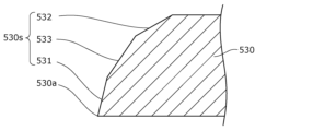
- FIG. 41 is a schematic cross-sectional view showing a cross section of a side surface 530s located on the periphery of the opening 530a of the insulating film 530 according to Modification 1. As shown in FIG. 41
- a side surface 530 s of the insulating film 530 located on the periphery of the opening 530 a has a lower side surface region 531 and an upper side surface region 532 arranged above the lower side surface region 531 .
- the side surface 530 s according to Modification 1 further has a middle side surface region 533 arranged between the lower side surface region 531 and the upper side surface region 532 .
- a semiconductor laser device having the insulating film 530 having such a structure also has the same effects as those of the above-described embodiments.
- a method for forming the opening 530a of the insulating film 530 according to Modification 1 will be described.
- a resist 95 is formed in the insulating film 530 in a region other than the region corresponding to the opening 530a.
- the first etching method is dry etching.
- a dry etching method for example, an ICP method with a frequency of 13.56 MHz can be used. Processing conditions used in dry etching are, for example, a top power of 120 W, a bias power of 40 W, a gas pressure of 1 Pa, and gas types of CHF 3 (flow rate 15 sccm) and CF 4 (flow rate 20 sccm). condition can be adopted.
- the region corresponding to the opening 530a in the insulating film 530 is etched by the second etching method by the second film thickness (second etching step).
- the second etching method is dry etching.
- the second etching method a method similar to the first etching method according to the first embodiment can be used.
- the region corresponding to the opening 530a in the insulating film 530 is etched by the third etching method by the third film thickness (third etching step).
- the third etching method is wet etching.
- the same method as the second etching method according to the first embodiment can be used as the third etching method.
- the opening 530a of the insulating film 530 can be formed by the method described above.
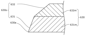
- FIG. 42 is a schematic cross-sectional view showing a cross section of a side surface 630s located on the periphery of the opening 630a of the insulating film 630 according to Modification 2. As shown in FIG. 42
- the insulating film 630 includes a lower insulating film 631m and an upper insulating film 632m arranged above the lower insulating film 631m and having a composition different from that of the lower insulating film 631m.
- the lower insulating film 631m is a silicon oxide film
- the upper insulating film 632m is a silicon nitride film.
- a side surface 630 s of the insulating film 630 located on the periphery of the opening 630 a has a lower side surface region 631 and an upper side surface region 632 arranged above the lower side surface region 631 .
- the lower side surface region 631 is formed in the lower insulating film 631m
- the upper side surface region 632 is formed in the upper insulating film 632m.
- the lower insulating film 631m having a lower etching rate in dry etching than the upper insulating film 632m can be used as an etching stop layer in the first etching process. Therefore, when forming the opening 630a, the first film thickness to be etched in the first etching step can be accurately controlled.
- a method for forming the opening 630a of the insulating film 630 according to Modification 2 will be described.
- a resist 95 is formed in a region of the insulating film 630 other than the region corresponding to the opening 630a.
- the region corresponding to the opening 630a in the insulating film 630 is etched by the first etching method by the first film thickness.
- the first etching method is dry etching.
- the first etching method for example, the same method as the first etching method according to Modification 1 can be used.
- the region corresponding to the opening 630a in the insulating film 630 is etched by the second etching method by the second film thickness.
- the second etching method is wet etching.
- a method similar to the second etching method according to the first embodiment can be used.
- the opening 630a of the insulating film 630 can be formed by the method described above.
- FIG. 43 is a schematic cross-sectional view showing the overall configuration of a semiconductor laser device 11 using the semiconductor laser element 10 according to Embodiment 1. As shown in FIG.
- the semiconductor laser device 11 includes a semiconductor laser element 10 and a submount 80. As shown in FIG. 43, the semiconductor laser device 11 includes a semiconductor laser element 10 and a submount 80. As shown in FIG. 43, the semiconductor laser device 11 includes a semiconductor laser element 10 and a submount 80. As shown in FIG. 43, the semiconductor laser device 11 includes a semiconductor laser element 10 and a submount 80. As shown in FIG. 43, the semiconductor laser device 11 includes a semiconductor laser element 10 and a submount 80.
- the submount 80 is a base on which the semiconductor laser element 10 is mounted.
- a pad electrode 60 of the semiconductor laser element 10 is bonded to the submount 80 .
- the submount 80 and the pad electrode 60 may be joined with AuSn solder, for example.
- Such a semiconductor laser device 11 includes the semiconductor laser element 10, the same effect as that of the semiconductor laser element 10 can be obtained.
- the semiconductor laser device 10 according to the first embodiment is used in FIG. 43, semiconductor laser devices according to other embodiments and modifications may be used.
- the semiconductor laser device emits blue-violet light, but the band of the emitted light from the semiconductor laser device is not limited to this.
- the semiconductor laser device may emit ultraviolet light.
- the nitride semiconductor laser element and the like of the present disclosure can be applied, for example, as a light source for processing machines as a highly efficient light source.
Landscapes
- Physics & Mathematics (AREA)
- Geometry (AREA)
- Condensed Matter Physics & Semiconductors (AREA)
- General Physics & Mathematics (AREA)
- Electromagnetism (AREA)
- Optics & Photonics (AREA)
- Semiconductor Lasers (AREA)
Priority Applications (2)
| Application Number | Priority Date | Filing Date | Title |
|---|---|---|---|
| CN202380022515.9A CN118715679A (zh) | 2022-02-22 | 2023-02-20 | 半导体激光元件及半导体激光元件的制造方法 |
| JP2024503137A JPWO2023162929A1 (https=) | 2022-02-22 | 2023-02-20 |
Applications Claiming Priority (2)
| Application Number | Priority Date | Filing Date | Title |
|---|---|---|---|
| JP2022025940 | 2022-02-22 | ||
| JP2022-025940 | 2022-02-22 |
Publications (1)
| Publication Number | Publication Date |
|---|---|
| WO2023162929A1 true WO2023162929A1 (ja) | 2023-08-31 |
Family
ID=87765811
Family Applications (1)
| Application Number | Title | Priority Date | Filing Date |
|---|---|---|---|
| PCT/JP2023/006020 Ceased WO2023162929A1 (ja) | 2022-02-22 | 2023-02-20 | 半導体レーザ素子、及び半導体レーザ素子の製造方法 |
Country Status (3)
| Country | Link |
|---|---|
| JP (1) | JPWO2023162929A1 (https=) |
| CN (1) | CN118715679A (https=) |
| WO (1) | WO2023162929A1 (https=) |
Citations (8)
| Publication number | Priority date | Publication date | Assignee | Title |
|---|---|---|---|---|
| JP2002261380A (ja) * | 2000-12-27 | 2002-09-13 | Furukawa Electric Co Ltd:The | 半導体装置およびその製造方法 |
| JP2004253545A (ja) * | 2003-02-19 | 2004-09-09 | Nichia Chem Ind Ltd | 窒化物半導体素子の製造方法及び窒化物半導体素子 |
| JP2006324427A (ja) * | 2005-05-18 | 2006-11-30 | Mitsubishi Electric Corp | 半導体レーザ |
| JP2007311591A (ja) * | 2006-05-19 | 2007-11-29 | Matsushita Electric Ind Co Ltd | 窒化物半導体レーザ装置及びその製造方法 |
| JP2010021206A (ja) * | 2008-07-08 | 2010-01-28 | Panasonic Corp | 半導体発光素子 |
| US20170054271A1 (en) * | 2014-04-11 | 2017-02-23 | Osram Opto Semiconductors Gmbh | Semiconductor Strip Laser and Semiconductor Component |
| WO2020110783A1 (ja) * | 2018-11-30 | 2020-06-04 | パナソニックセミコンダクターソリューションズ株式会社 | 半導体レーザ装置 |
| WO2021157027A1 (ja) * | 2020-02-06 | 2021-08-12 | 三菱電機株式会社 | 半導体装置及びその製造方法 |
-
2023
- 2023-02-20 JP JP2024503137A patent/JPWO2023162929A1/ja active Pending
- 2023-02-20 WO PCT/JP2023/006020 patent/WO2023162929A1/ja not_active Ceased
- 2023-02-20 CN CN202380022515.9A patent/CN118715679A/zh active Pending
Patent Citations (8)
| Publication number | Priority date | Publication date | Assignee | Title |
|---|---|---|---|---|
| JP2002261380A (ja) * | 2000-12-27 | 2002-09-13 | Furukawa Electric Co Ltd:The | 半導体装置およびその製造方法 |
| JP2004253545A (ja) * | 2003-02-19 | 2004-09-09 | Nichia Chem Ind Ltd | 窒化物半導体素子の製造方法及び窒化物半導体素子 |
| JP2006324427A (ja) * | 2005-05-18 | 2006-11-30 | Mitsubishi Electric Corp | 半導体レーザ |
| JP2007311591A (ja) * | 2006-05-19 | 2007-11-29 | Matsushita Electric Ind Co Ltd | 窒化物半導体レーザ装置及びその製造方法 |
| JP2010021206A (ja) * | 2008-07-08 | 2010-01-28 | Panasonic Corp | 半導体発光素子 |
| US20170054271A1 (en) * | 2014-04-11 | 2017-02-23 | Osram Opto Semiconductors Gmbh | Semiconductor Strip Laser and Semiconductor Component |
| WO2020110783A1 (ja) * | 2018-11-30 | 2020-06-04 | パナソニックセミコンダクターソリューションズ株式会社 | 半導体レーザ装置 |
| WO2021157027A1 (ja) * | 2020-02-06 | 2021-08-12 | 三菱電機株式会社 | 半導体装置及びその製造方法 |
Also Published As
| Publication number | Publication date |
|---|---|
| CN118715679A (zh) | 2024-09-27 |
| JPWO2023162929A1 (https=) | 2023-08-31 |
Similar Documents
| Publication | Publication Date | Title |
|---|---|---|
| EP2835885B1 (en) | Light emitting element and method of producing same | |
| JP4272239B2 (ja) | 半導体光素子の製造方法 | |
| CN109923742A (zh) | 发光元件及其制造方法 | |
| CN101361238A (zh) | 半导体激光元件及其制造方法 | |
| US11404849B2 (en) | Light emitting element to control an oscillation wavelength | |
| JP7623563B2 (ja) | 垂直共振器面発光レーザ素子 | |
| US11979001B2 (en) | Surface-emitting semiconductor laser | |
| US20070274360A1 (en) | Semiconductor laser element and semiconductor laser device | |
| JP6094632B2 (ja) | 半導体レーザ素子 | |
| JP7453588B2 (ja) | 垂直共振器面発光レーザ素子 | |
| JP2012094564A (ja) | 半導体レーザ素子およびその製造方法 | |
| US20200251884A1 (en) | Semiconductor laser element and method of manufacturing the same | |
| JP2009212386A (ja) | 半導体光素子の製造方法 | |
| CN114552385B (zh) | GaN基激光二极管结构及制造方法 | |
| JPWO2017038448A1 (ja) | 窒化物半導体素子 | |
| JP4640752B2 (ja) | 窒化ガリウム系半導体レーザ及びその製造方法 | |
| JP2006066660A (ja) | 窒化物半導体レーザ素子及びその製造方法 | |
| WO2023162929A1 (ja) | 半導体レーザ素子、及び半導体レーザ素子の製造方法 | |
| JP5872790B2 (ja) | 半導体レーザ装置 | |
| JP4983398B2 (ja) | 半導体レーザ素子 | |
| US20230335972A1 (en) | Semiconductor laser and semiconductor laser device | |
| US20230261438A1 (en) | Semiconductor laser and semiconductor laser device | |
| US20220416508A1 (en) | Semiconductor laser element | |
| US20220077368A1 (en) | Optoelectronic semiconductor device comprising portions of a conductive layer and method for manufacturing an optoelectronic semiconductor device | |
| JP2006013331A (ja) | 半導体レーザ素子 |
Legal Events
| Date | Code | Title | Description |
|---|---|---|---|
| 121 | Ep: the epo has been informed by wipo that ep was designated in this application |
Ref document number: 23759930 Country of ref document: EP Kind code of ref document: A1 |
|
| WWE | Wipo information: entry into national phase |
Ref document number: 2024503137 Country of ref document: JP |
|
| WWE | Wipo information: entry into national phase |
Ref document number: 202380022515.9 Country of ref document: CN |
|
| NENP | Non-entry into the national phase |
Ref country code: DE |
|
| 122 | Ep: pct application non-entry in european phase |
Ref document number: 23759930 Country of ref document: EP Kind code of ref document: A1 |