WO2023161757A1 - 半導体装置 - Google Patents
半導体装置 Download PDFInfo
- Publication number
- WO2023161757A1 WO2023161757A1 PCT/IB2023/051253 IB2023051253W WO2023161757A1 WO 2023161757 A1 WO2023161757 A1 WO 2023161757A1 IB 2023051253 W IB2023051253 W IB 2023051253W WO 2023161757 A1 WO2023161757 A1 WO 2023161757A1
- Authority
- WO
- WIPO (PCT)
- Prior art keywords
- conductor
- insulator
- transistor
- metal oxide
- oxide
- Prior art date
- Legal status (The legal status is an assumption and is not a legal conclusion. Google has not performed a legal analysis and makes no representation as to the accuracy of the status listed.)
- Ceased
Links
Images























Classifications
-
- H—ELECTRICITY
- H10—SEMICONDUCTOR DEVICES; ELECTRIC SOLID-STATE DEVICES NOT OTHERWISE PROVIDED FOR
- H10B—ELECTRONIC MEMORY DEVICES
- H10B53/00—Ferroelectric RAM [FeRAM] devices comprising ferroelectric memory capacitors
- H10B53/20—Ferroelectric RAM [FeRAM] devices comprising ferroelectric memory capacitors characterised by the three-dimensional [3D] arrangements, e.g. with cells on different height levels
-
- G—PHYSICS
- G11—INFORMATION STORAGE
- G11C—STATIC STORES
- G11C11/00—Digital stores characterised by the use of particular electric or magnetic storage elements; Storage elements therefor
- G11C11/21—Digital stores characterised by the use of particular electric or magnetic storage elements; Storage elements therefor using electric elements
- G11C11/22—Digital stores characterised by the use of particular electric or magnetic storage elements; Storage elements therefor using electric elements using ferroelectric elements
-
- H—ELECTRICITY
- H10—SEMICONDUCTOR DEVICES; ELECTRIC SOLID-STATE DEVICES NOT OTHERWISE PROVIDED FOR
- H10B—ELECTRONIC MEMORY DEVICES
- H10B12/00—Dynamic random access memory [DRAM] devices
-
- H—ELECTRICITY
- H10—SEMICONDUCTOR DEVICES; ELECTRIC SOLID-STATE DEVICES NOT OTHERWISE PROVIDED FOR
- H10B—ELECTRONIC MEMORY DEVICES
- H10B41/00—Electrically erasable-and-programmable ROM [EEPROM] devices comprising floating gates
- H10B41/70—Electrically erasable-and-programmable ROM [EEPROM] devices comprising floating gates the floating gate being an electrode shared by two or more components
-
- H—ELECTRICITY
- H10—SEMICONDUCTOR DEVICES; ELECTRIC SOLID-STATE DEVICES NOT OTHERWISE PROVIDED FOR
- H10B—ELECTRONIC MEMORY DEVICES
- H10B53/00—Ferroelectric RAM [FeRAM] devices comprising ferroelectric memory capacitors
-
- H—ELECTRICITY
- H10—SEMICONDUCTOR DEVICES; ELECTRIC SOLID-STATE DEVICES NOT OTHERWISE PROVIDED FOR
- H10B—ELECTRONIC MEMORY DEVICES
- H10B53/00—Ferroelectric RAM [FeRAM] devices comprising ferroelectric memory capacitors
- H10B53/30—Ferroelectric RAM [FeRAM] devices comprising ferroelectric memory capacitors characterised by the memory core region
-
- H—ELECTRICITY
- H10—SEMICONDUCTOR DEVICES; ELECTRIC SOLID-STATE DEVICES NOT OTHERWISE PROVIDED FOR
- H10D—INORGANIC ELECTRIC SEMICONDUCTOR DEVICES
- H10D1/00—Resistors, capacitors or inductors
- H10D1/60—Capacitors
- H10D1/68—Capacitors having no potential barriers
- H10D1/682—Capacitors having no potential barriers having dielectrics comprising perovskite structures
-
- H—ELECTRICITY
- H10—SEMICONDUCTOR DEVICES; ELECTRIC SOLID-STATE DEVICES NOT OTHERWISE PROVIDED FOR
- H10D—INORGANIC ELECTRIC SEMICONDUCTOR DEVICES
- H10D30/00—Field-effect transistors [FET]
- H10D30/01—Manufacture or treatment
- H10D30/021—Manufacture or treatment of FETs having insulated gates [IGFET]
-
- H—ELECTRICITY
- H10—SEMICONDUCTOR DEVICES; ELECTRIC SOLID-STATE DEVICES NOT OTHERWISE PROVIDED FOR
- H10D—INORGANIC ELECTRIC SEMICONDUCTOR DEVICES
- H10D30/00—Field-effect transistors [FET]
- H10D30/60—Insulated-gate field-effect transistors [IGFET]
- H10D30/67—Thin-film transistors [TFT]
- H10D30/674—Thin-film transistors [TFT] characterised by the active materials
- H10D30/6755—Oxide semiconductors, e.g. zinc oxide, copper aluminium oxide or cadmium stannate
-
- H—ELECTRICITY
- H10—SEMICONDUCTOR DEVICES; ELECTRIC SOLID-STATE DEVICES NOT OTHERWISE PROVIDED FOR
- H10D—INORGANIC ELECTRIC SEMICONDUCTOR DEVICES
- H10D30/00—Field-effect transistors [FET]
- H10D30/60—Insulated-gate field-effect transistors [IGFET]
- H10D30/68—Floating-gate IGFETs
-
- H—ELECTRICITY
- H10—SEMICONDUCTOR DEVICES; ELECTRIC SOLID-STATE DEVICES NOT OTHERWISE PROVIDED FOR
- H10D—INORGANIC ELECTRIC SEMICONDUCTOR DEVICES
- H10D30/00—Field-effect transistors [FET]
- H10D30/60—Insulated-gate field-effect transistors [IGFET]
- H10D30/69—IGFETs having charge trapping gate insulators, e.g. MNOS transistors
Definitions
- One embodiment of the present invention relates to semiconductor devices, memory devices, and electronic devices. Another embodiment of the present invention relates to a method for manufacturing a semiconductor device.
- one embodiment of the present invention is not limited to the above technical field.
- Technical fields of one embodiment of the present invention include semiconductor devices, display devices, light-emitting devices, power storage devices, storage devices, electronic devices, lighting devices, input devices (e.g., touch sensors), input/output devices (e.g., touch panels), The method of driving them or the method of manufacturing them can be given as an example.
- a semiconductor device in this specification and the like refers to all devices that can function by utilizing semiconductor characteristics.
- a semiconductor element such as a transistor, a semiconductor circuit, an arithmetic device, and a memory device are examples of semiconductor devices.
- a display device (a liquid crystal display device, a light-emitting display device, or the like), a projection device, a lighting device, an electro-optical device, a power storage device, a memory device, a semiconductor circuit, an imaging device, an electronic device, or the like can be said to include a semiconductor device in some cases.
- LSIs Large Scale Integration
- CPUs Central Processing Units
- memories storage devices
- DRAM Dynamic Random Access Memory
- SRAM Static Random Access Memory
- flash memory flash memory
- Patent Document 1 and Non-Patent Document 1 disclose a memory cell formed by stacking transistors.
- An object of one embodiment of the present invention is to provide a semiconductor device that can be miniaturized or highly integrated.
- An object of one embodiment of the present invention is to provide a semiconductor device that operates at high speed.
- An object of one embodiment of the present invention is to provide a semiconductor device with favorable electrical characteristics.
- An object of one embodiment of the present invention is to provide a semiconductor device in which variations in electrical characteristics of transistors are small.
- An object of one embodiment of the present invention is to provide a highly reliable semiconductor device.
- An object of one embodiment of the present invention is to provide a semiconductor device with high on-state current.
- An object of one embodiment of the present invention is to provide a semiconductor device with low power consumption.
- An object of one embodiment of the present invention is to provide a novel semiconductor device.
- An object of one embodiment of the present invention is to provide a method for manufacturing a semiconductor device in which the number of steps is small.
- An object of one embodiment of the present invention is to provide a storage device with a large storage capacity.
- An object of one embodiment of the present invention is to provide a memory device that occupies a small area.
- An object of one embodiment of the present invention is to provide a highly reliable storage device.
- An object of one embodiment of the present invention is to provide a memory device with low power consumption.
- An object of one embodiment of the present invention is to provide a novel storage device.
- One aspect of the present invention includes a first transistor, a second transistor, and a capacitor, where the first transistor includes a first insulator and a first metal on the first insulator. an oxide, a second insulator over the first metal oxide, a first conductor over the second insulator, and a portion of the top surface and a portion of the side surface of the first metal oxide; a second conductor overlying and a third conductor overlying a portion of the top surface and a portion of the side surface of the first metal oxide, the second transistor comprising the first insulator; a first metal oxide over the first insulator, a third insulator over the first metal oxide, a fourth conductor over the third insulator, and a third conductor and a fifth conductor covering part of the top surface and part of the side surface of the first metal oxide, and the third conductor includes the first transistor and the second transistor.
- the first metal oxide is shared by the first transistor and the second transistor, and the first metal oxide is shared by the channel formation region of the first transistor and the second transistor.
- the first insulator has a region overlapping with the first metal oxide; and the capacitor includes a sixth conductor, a seventh conductor, and a sixth conductor. and a material capable of having ferroelectricity positioned between the conductor and the seventh conductor, wherein the first conductor and the sixth conductor are electrically connected is.
- the material that can have ferroelectricity is preferably one or more selected from hafnium oxide, zirconium oxide, and HfZrO x (X is a real number greater than 0).
- the material that can have ferroelectricity is preferably a material containing oxygen, hafnium, and zirconium.
- the material that can have ferroelectricity is preferably a material obtained by adding one or more selected from zirconium, silicon, aluminum, gadolinium, yttrium, lanthanum, and strontium to hafnium oxide.
- the material that can have ferroelectricity is preferably zirconium oxide to which at least one selected from hafnium, silicon, aluminum, gadolinium, yttrium, lanthanum, and strontium is added.
- the eighth conductor preferably has a region sandwiched between the sixth conductor and the tenth conductor in plan view.
- the above structure includes a third transistor, the first insulator includes a material that can have ferroelectricity, and the third transistor includes an eighth conductor and an eighth conductor. a first insulator on the top, a second metal oxide on the first insulator, a fifth insulator on the second metal oxide, and a ninth conductor on the fifth insulator and a sixth conductor covering part of the top surface and part of the side surface of the second metal oxide, the sixth conductor having a region in contact with the top surface of the first insulator.
- the seventh conductor has a region in contact with the lower surface of the first insulator; the eighth conductor has a region in contact with the lower surface of the first insulator; preferably has a region overlapping with the second metal oxide and a region overlapping with the seventh conductor.
- the seventh conductor and the eighth conductor preferably contain titanium nitride.
- each of the plurality of memory layers includes a first transistor, a second transistor, and a capacitor, and each of the plurality of memory layers has a second transistor.
- the fifth conductors of the two transistors are preferably electrically connected to each other.
- a semiconductor device that can be miniaturized or highly integrated can be provided.
- a semiconductor device with high operating speed can be provided.
- a semiconductor device with favorable electrical characteristics can be provided.
- a semiconductor device with little variation in electrical characteristics of transistors can be provided.
- a highly reliable semiconductor device can be provided.
- a semiconductor device with high on-state current can be provided.
- a semiconductor device with low power consumption can be provided.
- One embodiment of the present invention can provide a novel semiconductor device.
- a method for manufacturing a semiconductor device in which the number of steps is small can be provided.
- a storage device with a large storage capacity can be provided.
- a memory device that occupies a small area can be provided.
- a highly reliable storage device can be provided.
- a memory device with low power consumption can be provided.
- An aspect of the present invention can provide a novel storage device.
- FIG. 1A and 1B are diagrams showing an example of a storage device.
- FIG. 2A is a diagram showing a circuit configuration example of a memory cell.
- FIG. 2B is a graph showing the amount of polarization.
- 3A, 3B, 3C, 3D, and 3E are diagrams showing operation examples of the memory cell.
- FIG. 4 is a diagram showing an operation example of a memory cell.
- 5A, 5B, and 5C are diagrams showing operation examples of the memory cell.
- 6A, 6B, and 6C are diagrams showing operation examples of the memory cell.
- FIG. 7 is a diagram showing an operation example of a memory cell.
- FIG. 8 is a cross-sectional view showing a configuration example of a semiconductor device.
- FIG. 8 is a cross-sectional view showing a configuration example of a semiconductor device.
- FIG. 9 is a cross-sectional view showing a configuration example of a semiconductor device.
- FIG. 10A is a cross-sectional view showing a configuration example of a semiconductor device.
- FIG. 10B is a cross-sectional view showing a configuration example of a transistor.
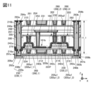
- FIG. 11 is a cross-sectional view showing a configuration example of a semiconductor device.
- FIG. 12 is a cross-sectional view showing a configuration example of a semiconductor device.
- FIG. 13 is a diagram showing a configuration example of a semiconductor device.
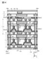
- FIG. 14 is a diagram showing a configuration example of a semiconductor device.
- FIG. 15 is a cross-sectional view showing a configuration example of a semiconductor device.
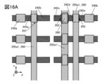
- 16A and 16B are plan views showing configuration examples of semiconductor devices.
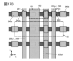
- 17A and 17B are plan views showing configuration examples of the semiconductor device.
- 18A and 18B are diagrams showing an example of a semiconductor device.
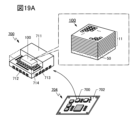
- 19A and 19B are diagrams showing an example of an electronic component.
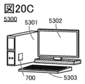
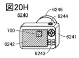
- 20A to 20J are diagrams illustrating examples of electronic devices.
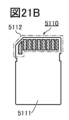
- 21A to 21E are diagrams illustrating examples of electronic devices.
- 22A to 22C are diagrams illustrating examples of electronic devices.
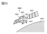
- FIG. 23 is a diagram showing an example of space equipment.
- the ordinal numbers “first” and “second” are used for convenience, and limit the number of constituent elements or the order of constituent elements (for example, the order of steps or the order of stacking). not something to do. Also, the ordinal number given to an element in one place in this specification may not match the ordinal number given to that element elsewhere in the specification or in the claims.
- film and “layer” can be interchanged depending on the case or circumstances.
- conductive layer can be changed to the term “conductive film.”
- insulating film can be changed to the term “insulating layer”.
- FIG. 1A shows a perspective schematic view of a storage device of one embodiment of the present invention.
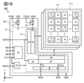
- FIG. 1B shows a block diagram of a storage device of one embodiment of the present invention.
- the memory device 100 shown in FIGS. 1A and 1B has a drive circuit layer 50 and n memory layers 11 .
- the memory layers 11 each have a memory cell array 15 .
- a memory cell array 15 has a plurality of memory cells 10 .
- the n-layer memory layer 11 is provided on the drive circuit layer 50 .
- the area occupied by the memory device 100 can be reduced. Also, the storage capacity per unit area can be increased.
- the first memory layer 11 is indicated as a memory layer 11_1, the second memory layer 11 is indicated as a memory layer 11_2, and the third memory layer 11 is indicated as a memory layer 11_3.
- the k-th layer (k is an integer of 1 or more and n or less) is indicated as a memory layer 11_k
- the n-th layer 11 is indicated as a memory layer 11_n.
- the term "storage layer 11" is simply used. sometimes.
- the drive circuit layer 50 has a PSW 22 (power switch), a PSW 23 and a peripheral circuit 31 .
- the peripheral circuit 31 has a peripheral circuit 41 , a control circuit 32 and a voltage generation circuit 33 .
- each circuit, each signal, and each voltage can be omitted as appropriate. Alternatively, other circuits or other signals may be added.
- Signal BW, signal CE, signal GW, signal CLK, signal WAKE, signal ADDR, signal WDA, signal PON1, and signal PON2 are input signals from the outside, and signal RDA is an output signal to the outside.
- Signal CLK is a clock signal.
- Signal BW, signal CE, and signal GW are control signals.
- Signal CE is a chip enable signal
- signal GW is a global write enable signal
- signal BW is a byte write enable signal.
- Signal ADDR is an address signal.
- the signal WDA is write data and the signal RDA is read data.
- a signal PON1 and a signal PON2 are power gating control signals. The signal PON1 and the signal PON2 may be generated by the control circuit 32.
- the control circuit 32 is a logic circuit having a function of controlling the overall operation of the storage device 100 .
- the control circuit logically operates the signal CE, the signal GW, and the signal BW to determine the operation mode (for example, write operation, read operation) of the memory device 100 .
- the control circuit 32 generates a control signal for the peripheral circuit 41 so that this operation mode is executed.
- the voltage generation circuit 33 has a function of generating a negative voltage.
- the signal WAKE has a function of controlling the input of the signal CLK to the voltage generation circuit 33 . For example, when an H level signal is applied to signal WAKE, signal CLK is input to voltage generation circuit 33, and voltage generation circuit 33 generates a negative voltage.
- the peripheral circuit 41 is a circuit for writing data to and reading data from the memory cell 10 .
- the peripheral circuit 41 has a row decoder 42 , a column decoder 44 , a row driver 43 , a column driver 45 , an input circuit 47 , an output circuit 48 and a sense amplifier 46 .
- Row decoder 42 and column decoder 44 have the function of decoding signal ADDR.
- Row decoder 42 is a circuit for specifying a row to be accessed
- column decoder 44 is a circuit for specifying a column to be accessed.
- the row driver 43 has a function of selecting the wiring WWL (write word line) or the wiring RWL (read word line) specified by the row decoder 42 .
- the column driver 45 has a function of writing data to the memory cells 10, a function of reading data from the memory cells 10, a function of holding the read data, and the like.
- the column driver 45 has a function of selecting the wiring WBL (write bit line) and the wiring RBL (read bit line) specified by the column decoder 44 .
- Input circuit 47 has a function of holding signal WDA. Data held by the input circuit 47 is output to the column driver 45 . Output data of the input circuit 47 is data (Din) to be written to the memory cell 10 . Data (Dout) read from the memory cells 10 by the column driver 45 is output to the output circuit 48 .
- the output circuit 48 has a function of holding Dout. Also, the output circuit 48 has a function of outputting Dout to the outside of the storage device 100 . Data output from the output circuit 48 is the signal RDA.
- PSW 22 has a function of controlling the supply of VDD to peripheral circuit 31 .
- PSW 23 has the function of controlling the supply of VHM to row driver 43 .
- the high power supply voltage of the memory device 100 is VDD
- the low power supply voltage is GND (ground potential).
- VHM is a high power supply voltage used to drive word lines to a high level and is higher than VDD.
- the signal PON1 controls ON/OFF of the PSW22, and the signal PON2 controls ON/OFF of the PSW23.
- the number of power supply domains to which VDD is supplied is set to one, but may be set to a plurality. In this case, a power switch may be provided for each power domain.
- FIG. 1B shows an example in which a memory cell array 15 has a plurality of memory cells 10 arranged in a matrix of p rows and q columns (p and q are integers of 2 or more).
- rows and columns extend in directions orthogonal to each other.
- the X direction is the “row” and the Y direction is the “column”, but the X direction may be the “column” and the Y direction the "row”.
- the memory cell 10 provided in the 1st row and the 1st column is indicated as memory cell 10[1,1] and the memory cell 10 provided in the pth row and qth column is indicated as memory cell 10[p,q]. showing.
- the memory cell 10 provided in the i-th row and the j-th column (i is an integer of 1 to p and j is an integer of 1 to q) is denoted as memory cell 10[i,j].
- FIG. 2A shows a circuit configuration example of a memory cell.
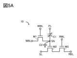
- the memory cell 10 has a transistor M1, a transistor M2, a transistor M3, and a capacitor C1.
- a memory cell including three transistors and one capacitor is also called a 3Tr1C memory cell. Therefore, the memory cell 10 described in this embodiment is a 3Tr1C memory cell.
- the gate of the transistor M1 is electrically connected to the wiring WWL[j], and one of the source and the drain is electrically connected to the wiring WBL[i,s].
- the wiring WBL[i,s] is electrically connected to one of the source and drain of the transistor M1 included in the memory cell 10[i,j] of the other stacked memory layer 11 .
- FIG. 2A shows a configuration example in which the wiring WWL[j] has a function of applying the gate potential of the transistor M1.
- Capacitor C1 has a pair of electrodes. One electrode of the capacitor C1 is electrically connected to the wiring PL[j], and the other electrode is electrically connected to the other of the source and the drain of the transistor M1.
- FIG. 2A shows a configuration example in which the wiring PL[j] has a function of applying a potential to one electrode of the capacitor C1.
- the gate of the transistor M2 is electrically connected to the other electrode of the capacitor C1
- one of the source and the drain is electrically connected to one of the source and the drain of the transistor M3, and the other of the source and the drain is connected to the wiring SL[ i, s].
- the wiring SL[i,s] is electrically connected to the other of the source and the drain of the transistor M2 included in the memory cell 10[i,j] of the other stacked memory layer 11 .
- the gate of the transistor M3 is electrically connected to the wiring RWL[j], and the other of the source and the drain is electrically connected to the wiring RBL[i,s].
- the wiring RBL[i,s] is electrically connected to the other of the source and drain of the transistor M3 included in the memory cell 10[i,j] of the other stacked memory layer 11 .
- the other electrode of the capacitor C, the other of the source or drain of the transistor M1, and the gate of the transistor M2 are electrically connected to each other, and a region always having the same potential is referred to as a “node SN”. call.
- the gate of the transistor M1 is electrically connected to the wiring WWL[j+1], and one of the source and the drain is electrically connected to the wiring WBL[i, s+1].
- the wiring WBL[i, s+1] is electrically connected to either the source or the drain of the transistor M1 included in the memory cell 10[i, j+1] of the other stacked memory layer 11 .
- FIG. 2A shows a configuration example in which the wiring WWL[j+1] has a function of applying the gate potential of the transistor M1.
- One electrode of the capacitor C1 is electrically connected to the wiring PL[j+1], and the other electrode is electrically connected to the other of the source and the drain of the transistor M1. Note that, for example, FIG.
- the wiring PL[j+1] has a function of applying a potential to one electrode of the capacitor C1.
- the gate of the transistor M2 is electrically connected to the other electrode of the capacitor C1
- one of the source and the drain is electrically connected to one of the source and the drain of the transistor M3
- the other of the source and the drain is connected to the wiring SL[ i, s+1].
- the wiring SL[i, s+1] is electrically connected to the other of the source and the drain of the transistor M2 included in the memory cell 10[i, j+1] of the other stacked memory layer 11 .
- the gate of the transistor M3 is electrically connected to the wiring RWL[j+1], and the other of the source and the drain is electrically connected to the wiring RBL[i,s].
- the wiring RBL[i,s] is electrically connected to the other of the source and the drain of the transistor M3 included in the memory cell 10[i,j+1] of the other stacked memory layer 11 .
- the wiring RBL[i,s] corresponds to the other of the source or drain of the transistor M3 included in the memory cell 10[i,j] and the other of the source or drain of the transistor M3 included in the memory cell 10[i,j+1]. is electrically connected to Therefore, the wiring RBL[i,s] functions as a wiring for transmitting signals to the memory cells 10 located in adjacent columns.
- the wiring RBL[i,s] functions as a wiring that transmits a signal to the memory cell 10[i,j] and the memory cell 10[i,j+1].
- the wiring WBL[i,s] supplies signals to the memory cells 10 located in adjacent columns, for example, the memory cells 10[i,j ⁇ 1] and 10[i,j].
- the wiring WBL[i,s+1] transmits signals to the memory cells 10 located in adjacent columns, for example, the memory cells 10[i,j+1] and 10[i,j+2]. functions as a wire to transmit the
- the wiring SL[i,s] supplies signals to the memory cells 10 located in adjacent columns, for example, the memory cells 10[i,j ⁇ 1] and 10[i,j].
- the wiring SL[i, s+1] transmits a signal to the memory cells 10 located in adjacent columns, for example, the memory cells 10 [i, j+1] and 10 [i, j+2]. functions as a wire to transmit the
- a region in which the other electrode of the capacitor C1, the other of the source or drain of the transistor M1, and the gate of the transistor M2 are electrically connected to each other and always at the same potential is called a node SN. .
- transistors each having a back gate may be used as the transistor M1, the transistor M2, and the transistor M3.
- the gate and the back gate are arranged so as to sandwich the semiconductor channel forming region between the gate and the back gate.
- the gate and back gate are made of conductors.
- a back gate can function like a gate. Further, by changing the potential of the back gate, the threshold voltage of the transistor can be changed.
- the potential of the back gate may be the same potential as that of the gate, the ground potential, or an arbitrary potential.
- each of the transistor M1, the transistor M2, and the transistor M3 does not have to have a back gate.
- the gate and back gate are made of conductors, they also have a function of preventing an electric field generated outside the transistor from acting on the semiconductor in which the channel is formed (particularly, an electrostatic shielding function against static electricity). That is, it is possible to suppress fluctuations in the electrical characteristics of the transistor due to the influence of an external electric field such as static electricity.
- the amount of change in the threshold voltage of the transistor before and after a BT (Bias Temperature) test can be reduced by providing the back gate.
- the transistor M1 By using a transistor having a back gate as the transistor M1, the influence of an external electric field is reduced and the transistor M1 can be stably kept off. Therefore, the data written to the node SN can be held stably.
- the back gate By providing the back gate, the operation of the memory cell 10 is stabilized, and the reliability of the memory device including the memory cell 10 can be improved.
- the transistor M3 by using a transistor having a back gate as the transistor M3, the influence of an external electric field is reduced, and the transistor M3 can be stably kept off. Therefore, leakage current between the wiring RBL and the wiring SL is reduced, and power consumption of the memory device including the memory cell 10 can be reduced.
- a semiconductor device of one embodiment of the present invention includes a transistor including an oxide semiconductor, which is a kind of metal oxide, in a semiconductor layer in which a channel is formed (also referred to as an “OS transistor”).
- An OS transistor has a higher withstand voltage between a source and a drain than a transistor using silicon for a semiconductor layer in which a channel is formed (also referred to as a Si transistor).
- the memory cell 10 has sufficient resistance to the inversion polarization voltage of the ferroelectric layer, and the rewrite resistance of the memory cell 10 can be improved.
- the OS transistor since the OS transistor has high frequency characteristics, the semiconductor device can read and write data at high speed.
- OS transistors are preferably used as the transistor M1, the transistor M2, and the transistor M3.
- An oxide semiconductor has a bandgap of 2 eV or more, and thus has a significantly low off-state current. Therefore, power consumption of the memory cell 10 can be reduced. Therefore, the power consumption of the memory device 100 including the memory cells 10 can be reduced.
- a semiconductor layer in which channels of the transistors M1, M2, and M3 are formed a single crystal semiconductor, a polycrystalline semiconductor, a microcrystalline semiconductor, an amorphous semiconductor, or the like may be used alone or in combination.
- Silicon or germanium for example, can be used as the semiconductor material.
- Compound semiconductors such as silicon germanium, silicon carbide, gallium arsenide, oxide semiconductors, or nitride semiconductors may also be used.
- a memory cell including an OS transistor can also be called an "OS memory.” Further, the memory device 100 including the memory cell can also be called an "OS memory”.
- the OS transistor operates stably even in a high-temperature environment and has little characteristic variation.
- the off current hardly increases even in a high temperature environment.
- the off current hardly increases even under an environmental temperature of room temperature or higher and 200° C. or lower.
- the on-current is less likely to decrease even in a high-temperature environment. Therefore, the OS memory can operate stably even in a high-temperature environment and obtain high reliability.
- OS transistors have better electrical characteristics than Si transistors in high-temperature environments. Specifically, even at a high temperature of 100° C. to 200° C., preferably 125° C. to 150° C., the ratio of the on-current to the off-current is large, so that good switching operation can be performed.
- a ferroelectric is preferably used as the dielectric of the capacitor C1.
- the storage device of one embodiment of the present invention can retain data for a long time. Accordingly, the frequency of refreshing (rewriting data to cells) can be reduced, so that power consumption of the memory device of one embodiment of the present invention can be reduced.
- the capacitor provided with the ferroelectric layer between the first electrode and the second electrode retains data for a long time without adopting a structure for increasing the capacitance, such as a trench structure. be able to. As a result, a storage device having an easy-to-manufacture structure can be obtained.
- Capacitors with ferroelectric layers are sometimes called ferroelectric capacitors.
- a capacitor with a ferroelectric layer when a voltage (electric field or electric field) is applied between two electrodes sandwiching the ferroelectric layer, the ferroelectric layer changes depending on the direction and amount of voltage application. The direction of polarization and the amount of polarization change. Signals (data) are stored (written) between two electrodes sandwiching the ferroelectric layer using the change in the polarization state of the ferroelectric layer. After data is stored (written) into the capacitor, polarization remains in the ferroelectric layer (residual polarization) even when the voltage between the two electrodes sandwiching the ferroelectric layer is reduced to zero. In order to rewrite the polarization, a voltage for reversing the polarization (polarization reversal voltage) is applied.
- FIG. 2B is a graph showing the magnitude of polarization (polarization amount) according to the electric field applied to the ferroelectric layer.
- the horizontal axis indicates the electric field E applied to the ferroelectric layer.
- the vertical axis indicates the amount of polarization P of the ferroelectric layer.
- the polarization of the ferroelectric layer increases.
- the electric field applied to the ferroelectric layer is lowered after the electric field EH is applied to the ferroelectric layer, positive charges are biased toward one electrode side of the capacitor, and negative charges are biased toward the other electrode side of the capacitor. Because of the bias, positive polarization remains when the electric field becomes zero.
- the electric field applied to the ferroelectric layer is lowered, the polarization of the ferroelectric layer becomes smaller.
- the electric field applied to the ferroelectric layer is increased after the electric field EL is applied to the ferroelectric layer, the positive charges are biased toward the other electrode side of the capacitor C1, and the negative charges are biased toward the one electrode side of the capacitor.
- a voltage for applying the electric field EH and the electric field EL to the ferroelectric layer can be called a polarization reversal voltage.
- Data can be written to the memory cell 10 by applying a polarization inversion voltage to the capacitor C1.
- the electric field E R can be, for example, an electric field (coercive electric field) in which the polarization becomes zero.
- the voltage for applying the electric field E R to the ferroelectric layer can be said to be the voltage that does not cause polarization reversal.
- a voltage that does not cause polarization inversion to the capacitor C1 it is possible to read out data from the memory cell 10 by amplifying the change in potential corresponding to the amount of change in polarization (P H , P L ).
- a negative electric field is shown as the electric field ER , but it may be a positive electric field.
- the memory device including the memory cell 10 is excellent in reliability of read data.
- the memory device including the memory cell 10 can achieve low power consumption.
- the area of the capacitor can be reduced as compared with a capacitor having a paraelectric.
- Materials that can be used for the ferroelectric layer and can have ferroelectricity include hafnium oxide, zirconium oxide, HfZrO x (X is a real number greater than 0), hafnium oxide and element J1 (here, The element J1 is a material to which zirconium (Zr), silicon (Si), aluminum (Al), gadolinium (Gd), yttrium (Y), lanthanum (La), strontium (Sr), etc.) is added, and an element to zirconium oxide.
- element J2 here is hafnium (Hf), silicon (Si), aluminum (Al), gadolinium (Gd), yttrium (Y), lanthanum (La), strontium (Sr), etc.) added material , and so on.
- the atomic ratio of the hafnium atoms and the element J1 can be appropriately set.
- the ratio of hafnium atoms and zirconium atoms may be 1:1 or in the vicinity thereof.
- the ratio of the number of atoms of the zirconium atoms and the element J2 can be set as appropriate.
- Materials that can have ferroelectricity include PbTiO x , barium strontium titanate (BST), strontium titanate, lead zirconate titanate (PZT), strontium bismuthate tantalate (SBT), and bismuth ferrite (BFO). , barium titanate, and other piezoelectric ceramics having a perovskite structure may also be used.
- a material that can have ferroelectricity for example, a plurality of materials selected from the materials listed above, or a laminated structure composed of a plurality of materials selected from the materials listed above can be used. can.
- hafnium oxide, zirconium oxide, HfZrO x , and materials obtained by adding the element J1 to hafnium oxide may change their crystal structures (characteristics) depending not only on film formation conditions but also on various processes.
- materials exhibiting ferroelectricity are called ferroelectrics, but also materials capable of having ferroelectricity or materials having ferroelectricity are called.
- Materials that can have ferroelectricity include scandium aluminum nitride (Al1 - aScaNb (a is a real number greater than 0 and less than 0.5, and b is 1 or a value in the vicinity thereof ). hereinafter simply referred to as AlScN)), Al--Ga--Sc nitrides, Ga--Sc nitrides, and the like can be used.
- AlScN scandium aluminum nitride
- Al-Ga--Sc nitrides Al--Ga--Sc nitrides
- Ga--Sc nitrides and the like
- a metal nitride containing an element M1, an element M2, and nitrogen can be used as a material that can have ferroelectricity.
- the element M1 is one or more selected from aluminum (Al), gallium (Ga), indium (In), and the like.
- Element M2 includes boron (B), scandium (Sc), yttrium (Y), lanthanides (lanthanum (La), cerium (Ce), praseodymium (Pr), neodymium (Nd), promethium (Pm), samarium ( Sm), europium (Eu), gadolinium (Gd), terbium (Tb), dysprosium (Dy), holmium (Ho), erbium (Er), thulium (Tm), ytterbium (Yb), and lutetium (Lu)), Actinide (15 elements from actinium (Ac) to lawrencium (Lr)), titanium (Ti), zirconium (Zr), hafnium (Hf), vanadium (V), niobium (Nb), tantalum (Ta), chromium ( Cr) and the like.
- Actinide (15 elements from actinium (Ac) to lawrencium (Lr)),
- the ratio between the number of atoms of the element M1 and the number of atoms of the element M2 can be set as appropriate.
- a metal oxide containing the element M1 and nitrogen may have ferroelectricity even if it does not contain the element M2.
- a material that can have ferroelectricity a material obtained by adding an element M3 to the metal nitride can be used.
- Element M3 is one or more selected from magnesium (Mg), calcium (Ca), strontium (Sr), zinc (Zn), cadmium (Cd), and the like.
- the ratio of the number of atoms of the element M1, the number of atoms of the element M2, and the number of atoms of the element M3 can be set as appropriate.
- the metal nitride contains at least a group 13 element and nitrogen, which is a group 15 element
- the metal nitride is used as a group 13-15 ferroelectric and a strong material of a group 13 nitride. They are sometimes called dielectrics.
- perovskite-type oxynitrides such as SrTaO 2 N and BaTaO 2 N, GaFeO 3 with a ⁇ -alumina structure, and the like can be used.
- the material that can have ferroelectricity can be, for example, a mixture or a compound composed of a plurality of materials selected from the materials listed above.
- the material that can have ferroelectricity can have a laminated structure composed of a plurality of materials selected from the materials listed above.
- the materials listed above may also be called materials capable of having ferroelectricity or materials having ferroelectricity.
- a hafnium oxide layer or a layer containing hafnium oxide and zirconium oxide is preferable as a ferroelectric layer because it can have ferroelectricity even if it is processed into a thin film of several nm.
- a ferroelectric layer that can be thinned a memory device combined with a miniaturized transistor can be obtained.
- HfZrO X when used as a material capable of having ferroelectricity, it is preferable to use an atomic layer deposition (ALD) method, particularly a thermal ALD method, for film formation. Further, in the case of forming a film of a material that can have ferroelectricity by using the thermal ALD method, it is preferable to use a material that does not contain hydrocarbon (hydrocarbon, also called HC) as a precursor. When one or both of hydrogen and carbon are contained in the material that can have ferroelectricity, crystallization of the material that can have ferroelectricity may be inhibited.
- ALD atomic layer deposition
- hydrocarbon-free precursors include chlorine-based materials.
- HfZrO x hafnium oxide and zirconium oxide
- one or both of HfCl 4 and ZrCl 4 may be used as the precursor.
- the ALD method is a film forming method in which a precursor and a reactant (for example, an oxidizing agent) are alternately introduced, and since the film thickness can be adjusted by the number of times this cycle is repeated, precise film thickness adjustment is possible. be.
- heat treatment for example, an RTA (Rapid Thermal Anneal) device, a resistance heating furnace, or a microwave heating device can be used.
- RTA Rapid Thermal Anneal
- a resistance heating furnace for example, a resistance heating furnace, or a microwave heating device.
- a film having particularly excellent ferroelectricity may be obtained, which is preferable.
- impurities in the film here at least one of hydrogen, hydrocarbon, and carbon, are thoroughly eliminated to obtain a highly pure intrinsic film. It is possible to form a film having good ferroelectricity. Note that a highly purified intrinsic ferroelectric film and a highly purified intrinsic oxide semiconductor described in an embodiment described later have very high compatibility in manufacturing processes. Therefore, a method for manufacturing a memory device with high productivity can be provided.
- HfZrO 2 X when used as a material capable of having ferroelectricity, it is preferable to alternately deposit hafnium oxide and zirconium oxide so as to have a composition of 1:1 using thermal ALD.
- H 2 O or O 3 can be used as an oxidizing agent.
- the oxidizing agent for the thermal ALD method is not limited to this.
- the oxidizing agent for the thermal ALD method may include any one or more selected from O2 , O3 , N2O , NO2 , H2O , and H2O2 .
- the crystal structure of the material that can have ferroelectricity is not particularly limited.
- the crystal structure of a material that can have ferroelectricity may be one or more selected from a cubic system, a tetragonal system, a rectangular system, and a monoclinic system.
- a material that can have ferroelectricity it is preferable to have a cubic crystal structure because ferroelectricity is exhibited.
- a composite structure having an amorphous structure and a crystalline structure may be used as a material capable of having ferroelectricity.
- the wiring WBL is a wiring to which a signal (data signal) corresponding to data written to the memory cell 10 is supplied.
- the wiring WBL may also be called a write bit line.
- the wiring WBL can be a wiring shared with another wiring, for example, the wiring RBL.
- the wiring WWL is a wiring supplied with a signal (selection signal) for writing data to the memory cell 10 .
- the wiring WWL may also be called a write word line.
- the wiring PL is supplied with a signal (control signal) for writing data to the memory cell 10 and a signal (control signal) for reading data from the memory cell 10 .
- the wiring PL has a function of controlling the polarization state of the ferroelectric layer of the capacitor C1, and is sometimes referred to as a polarization control line.
- the wiring SL is a wiring supplied with a constant potential for reading data from the memory cell 10 .
- the wiring SL has a function of allowing current to flow between it and the wiring RBL according to data stored in the memory cell 10, and is sometimes called a source line.
- the wiring RBL is a wiring supplied with a signal according to data read from the memory cell 10 .
- the wiring RBL may also be called a read bit line.
- the wiring RBL can be a wiring shared with another wiring, for example, the wiring WBL.
- each transistor is described as an n-channel transistor.
- the transistor M1 can be turned on by setting the wiring WWL to a high potential (also referred to as an H-level potential or H-level).
- the wiring WWL is set to a low potential (also referred to as an L-level potential or an L-level)
- the transistor M1 can be turned off. The same is true for the transistor M3.
- Data is written to the memory cell 10 according to the direction of the electric field applied to the ferroelectric layer of the capacitor C1 given by the potential of the node SN and the potential of the wiring PL.
- the data signal to be written applies a polarization inversion voltage to the capacitor C1.
- the ferroelectric layer of the capacitor C1 can assume different polarization states depending on the data signal.
- the capacitance value of the capacitor C1 can be varied according to this polarization state. This polarization state and the difference in the capacitance value of the capacitor C1 are maintained even when the electric field to the capacitor C1 is zero.
- Data is read from the memory cell 10 using capacitive coupling at the capacitor C1 when the potential of the wiring PL is changed.
- the potential of the wiring PL is set so that the voltage applied to the capacitor C1 does not reverse the polarization of the ferroelectric layer.
- capacitive coupling occurs in the capacitor C1. Therefore, the potential of the node SN changes according to a change in the potential of the wiring PL.
- a change in the potential of the node SN differs depending on the state of the capacitance value of the capacitor C1. Therefore, the potential of the gate of the transistor M2 can be varied according to the stored data.
- the different potentials of the gates of the transistors result in different amounts of current flowing between the source and drain of the transistor M2. Data can be read from the memory cell 10 based on the difference in current amount.
- FIG. 3A is a timing chart for explaining the data write operation in the memory cell 10 shown in FIG. 2A.
- FIG. 3A shows signals or potentials of the wiring WWL, the wiring WBL, the wiring PL, the node SN, the wiring RBL, the wiring RWL, and the wiring SL in the memory cell 10 .
- FIG. 3A also shows “data1” and “data0” as data to be written in the memory cell 10 .
- “data1” is shown as an H level signal
- “data0” is shown as an L level signal.
- the wiring WWL is set to H level.
- a signal corresponding to data data1 or data0 to be written to the memory cell 10 is applied to the wiring WBL, and a potential corresponding to the signal is applied to the node SN.
- the wiring PL is set to H level.
- the wiring RBL, the wiring RWL, and the wiring SL are set to L level.
- An H-level signal applied to the wiring WBL, the wiring PL, and the node SN is indicated as a potential VPL1, and an L-level signal is indicated as a potential 0V.
- the potential VPL1 is a potential at which the potential VPL1 is applied to one electrode of the capacitor C1 and a potential of 0 V is applied to the other electrode, thereby applying a reverse polarization voltage to the ferroelectric layer of the capacitor C1.
- Potential VPL1 is preferably 2.5 V or higher.
- the transistors M1 to M3 are preferably transistors with high resistance (withstand voltage) to high voltage.
- the rewrite resistance of the memory cell 10 can be improved by forming the transistors M1 to M3 with OS transistors having higher withstand voltage characteristics than Si transistors.
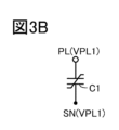
- the potential shown in FIG. 3B is applied to the electrode of the capacitor C1.
- the electrodes at both ends of the capacitor C1 are both at the same potential as the potential VPL1, so that no voltage exceeding the inversion polarization voltage is applied and no electric field is generated on the ferroelectric layer.
- the potential shown in FIG. 3C is applied to the electrode of the capacitor C1. As shown in FIG.
- a voltage VPL1 which is an inversion polarization voltage, is applied to the electrodes of the capacitor C1, and an electric field EL is generated in the ferroelectric layer. Therefore, the polarization state corresponding to data0 is written into the capacitor C1.
- the wiring WWL is set to the H level following the period P11.
- a signal corresponding to data data1 or data0 to be written to the memory cell 10 is applied to the wiring WBL in the period P11, and a potential corresponding to the signal is applied to the node SN.
- the wiring PL is set to L level.
- the wiring RBL, the wiring RWL, and the wiring SL are set to L level.
- the potential shown in FIG. 3D is applied to the electrode of the capacitor C1.
- an electric field opposite to the period P11 is applied to the pair of electrodes of the capacitor C1
- a voltage VPL1 that is an inversion polarization voltage is applied to the electrodes of the capacitor C1
- the electric field is applied to the ferroelectric layer. EH is produced. Therefore, the polarization state corresponding to data1 is written into the capacitor C1.
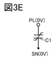
- the electrodes of the capacitor C1 are both at the same potential as the potential 0 V, as shown in FIG. 3E. It is not applied and does not create an electric field on the ferroelectric layer.
- FIG. 4 is a timing chart for explaining the data read operation in the memory cell 10 shown in FIG.
- FIG. 4 shows signals or potentials of the wiring WWL, the wiring WBL, the wiring PL, the node SN, the wiring RBL, the wiring RWL, and the wiring SL in the memory cell 10 .
- FIG. 4 also shows “data1” and “data0” as data read from the memory cell 10 .
- "data1" and “data0” correspond to the data stored as the polarization state of the ferroelectric layer of the capacitor C1 in the data write operation.
- the wiring WWL is at L level. Node SN is in an electrically floating state.
- the wiring PL is set to the potential VPL2.
- the wiring WBL, the wiring RWL, and the wiring SL are set to L level.
- the wiring RBL is precharged to a potential that varies depending on the currents flowing through the transistors M2 and M3 in a period before the period P21. For example, it is precharged to a potential lower than the potential VPL1.
- the node SN in the memory cell 10 has a capacitance C2 that is a parasitic capacitance such as the gate capacitance of the transistor M2.
- C2 a parasitic capacitance such as the gate capacitance of the transistor M2.
- the amount of change ⁇ V SN in the potential V SN of the node SN is determined by the capacitance value C FE of the capacitor C1, the capacitance value C S of the capacitor C2, and the amount of change ⁇ VPL2 in the voltage VPL2 corresponding to the voltage of the capacitor C1. can be represented.
- the capacitance value CFE of the capacitor C1 is determined by the polarization state of the ferroelectric layer of the capacitor C1. This polarization state differs according to the written data "data1" or “data0". Therefore, the potential VSN of the node SN can be changed depending on the written data "data1" or "data0".
- the capacitance value CS of the parasitic capacitance (capacitor C2) of the node SN is smaller than the capacitance value CFE of the capacitance C1 having the ferroelectric layer.
- a potential difference due to a difference in capacitance value according to the polarization state of the capacitor C1 appears as Vdata0 or Vdata1 in the potential VSN of the node SN.
- the wiring RWL is set to H level. Conduction is established between the source and the drain of the transistor M3. A current corresponding to the potential of the node SN flows through the transistor M2.
- the potential of the node SN can take two states of potential Vdata0 and potential Vdata1 (>Vdata0) as illustrated in FIGS. 5B and 5C.
- a current Idata0 or Idata1 (>Idata0) according to the potential Vdata0 or Vdata1 flows through the transistor M2.
- the potential of the precharged wiring RBL changes due to the flow of the current Idata0 or Idata1.
- the potential of the wiring RBL after the change is determined according to the magnitude of the current (Idata0 or Idata1) flowing through the transistor M2.
- Whether the written data is “data1” or “data0” is determined by comparing the magnitude relationship between the potential of the wiring RBL after the change and the reference voltage VREF , and data is read from the memory cell 10 . can be done.
- the potential of the wiring RBL becomes higher than the reference voltage VREF . lower than the voltage V - - REF .
- the potential of the wiring RBL to be precharged is preferably lower than the potential VPL1. With this structure, fluctuation in the potential of the wiring RBL can be reduced. Therefore, even if a circuit including a transistor electrically connected to the wiring RBL is a miniaturized transistor such as a Si transistor and has a low withstand voltage, the circuit can be operated without problems.
- the operation of reading data from the memory cell 10 in FIG. 2A can be configured differently. For example, it may be operated as shown in the timing chart of FIG. 6A.
- the potential of the wiring SL is increased, and a current corresponding to the potential of the node SN is flowed while the wiring RBL is precharged to 0V. That is, as illustrated in FIGS. 6B and 6C, a current Idata0 or Idata1 (>Idata0) corresponding to the potential Vdata0 or Vdata1 flows through the transistor M2 from the wiring SL toward the wiring RBL.
- Data can be read from the memory cell 10 by comparing the magnitude relationship between the potential of the wiring RBL and the reference voltage VREF .
- the potential of the wiring RBL becomes lower than the reference voltage VREF . higher than the voltage V-- REF .
- the operation of reading data from the memory cell 10 of FIG. 2A can be performed in another operation method. For example, it may be operated as shown in the timing chart of FIG.
- FIG. 7 corresponds to the operation method in which the operation of setting the potential of the node SN is added to FIG.
- the potential of the wiring WBL is set to a desired potential VPRE_SN
- the potential of the wiring WWL is set to H level.
- the potential of the node SN becomes the potential VPRE_SN .
- the wiring WWL is set to L level, and the node SN is kept in an electrically floating state.
- the potential of the node SN which changes when the potential of the wiring PL is changed in the period P21, can be easily set to the current that the transistor M2 flows.
- One embodiment of the present invention relates to a semiconductor device in which a memory layer is provided over a substrate.
- the memory layer has a first transistor, a second transistor, a third transistor, and a capacitor, which can constitute a memory cell. Since a semiconductor device of one embodiment of the present invention includes memory cells, it has a function of storing data. Therefore, a semiconductor device of one embodiment of the present invention can be called a memory device.
- a plurality of memory layers having the above structure are stacked.
- a plurality of memory layers having the above structure are provided, for example, in a direction perpendicular to the substrate surface.
- the OS transistor a semiconductor layer in which a channel is formed can be formed by a thin film method such as a sputtering method.
- the OS transistor can be formed at a low temperature, for example, a temperature of 750° C. or lower. Therefore, a plurality of layers each including an OS transistor can be stacked.
- An OS transistor can be preferably used for a plurality of stacked memory layers.
- the OS transistor can be freely arranged by stacking it on a circuit using a Si transistor or the like, integration can be easily performed.
- silicon for example, amorphous silicon (sometimes referred to as hydrogenated amorphous silicon), microcrystalline silicon, polycrystalline silicon, monocrystalline silicon, or the like can be used.
- an OS transistor can be manufactured using a manufacturing apparatus similar to that of a Si transistor, it can be manufactured at low cost.
- a gain cell type memory cell requires at least two transistors per memory cell, and it is difficult to increase the number of memory cells that can be arranged per unit area. , a plurality of memory cell arrays 15 can be stacked. That is, the amount of data that can be stored per unit area can be increased.
- the write bit line and the read bit line can be provided, for example, in a direction perpendicular to the substrate surface.
- n is an integer of 2 or more
- an opening is provided to penetrate the n storage layers, and a conductor is formed inside the opening.
- write bit lines, and read bit lines can be formed.
- a conductor having regions functioning as write bit lines is provided so as to have regions in contact with the top surface and side surfaces of the first conductor.
- FIG. 8 is a cross-sectional view illustrating a structural example of a semiconductor device of one embodiment of the present invention.
- the semiconductor device shown in FIG. 8 can be applied to the circuit configuration of the memory cell shown in the above embodiment.
- insulator 8 includes an insulator 210 over a substrate (not shown), conductors 209a and 209b embedded in the insulator 210, an insulator 212 over the insulator 210, and an insulator
- the insulator 214 on the insulator 212, the n-layer storage layer 11 on the insulator 214, and the n-layer extending in the Z direction are provided so as to be conductive.
- the components included in the semiconductor device of this embodiment may each have a single-layer structure or a laminated structure.
- the conductor 209 may be used when describing items common to the conductor 209a and the conductor 209b.
- a memory cell array having a plurality of memory cells is provided in each of the memory layers 11_1 to 11_n.
- a memory cell includes a transistor 201 , a transistor 202 , a transistor 203 , and a capacitor 101 .
- the conductor 240a has a region that functions as a write bit line
- the conductor 240b has a region that functions as a read bit line.
- the transistor 201, the transistor 202, the transistor 203, and the capacitor 101 can correspond to the transistor M1, the transistor M2, the transistor M3, and the capacitor C1 included in the memory cell 10 described in the above embodiment, respectively.
- the conductor 240a and the conductor 240b can correspond to the wiring WBL and the wiring RBL, respectively.
- the direction parallel to the channel length direction of the illustrated transistor is defined as the X direction
- the direction parallel to the channel width direction of the illustrated transistor is defined as the Y direction.
- the X and Y directions may be directions perpendicular to each other.
- the direction perpendicular to both the X direction and the Y direction ie, the direction perpendicular to the XY plane, is defined as the Z direction.
- the X direction and Y direction can be, for example, parallel to the substrate surface, and the Z direction can be perpendicular to the substrate surface.
- the conductors 209a and 209b function as parts of circuit elements such as switches, transistors, capacitors, inductors, resistors, and diodes, wirings, electrodes, or terminals.
- FIG. 8 shows a memory layer 11_1 as the lowest layer, a memory layer 11_2 above the memory layer 11_1, and a memory layer 11_n as the top layer among the n memory layers.
- the conductors 209 a and 209 b are electrically connected to a driver circuit for driving memory cells provided in the memory layer 11 .
- the driver circuit is provided below the conductors 209a and 209b.
- the transistors 201 , 202 , and 203 are provided over the insulator 214 . Here, the transistors 202 and 203 share some layers.
- a capacitor 101 is provided above the transistors 201 to 203 .
- FIG. 9 shows an example having connection electrodes 240c and 240d instead of the conductors 240a and 240b.
- the memory layer 11 is electrically connected to a conductor 233a electrically connected to a conductor 242a (detailed in FIG. 10) included in the transistor 201 and a conductor 242e (detailed in FIG. 10) included in the transistor 203. and a conductor 233b connected to the .
- the conductor 233a and the conductor 233b included in the memory layer 11 — k which is the k-th memory layer 11 (k is an integer of 1 or more and n or less), are represented as a conductor 233a[k] and a conductor 233b[k], respectively. .
- connection electrode 240c has conductors 233a[1] to 233a[n] (not shown), which are electrically connected.
- connection electrode 240d includes conductors 233b[1] to 233b[n] (not shown), which are electrically connected.
- FIG. 10A is a cross-sectional view showing a structural example of the conductor 209a, the conductor 209b, the insulator 210, the insulator 212, the insulator 214, and the memory layer 11_1.
- an insulator 282 is provided over the transistors 201 to 203 and an insulator 285 is provided over the insulator 282 .
- the transistor 201, the transistor 202, and the transistor 203 include a conductor 205a1 over the insulator 214, an insulator 222 over the conductor 205a1, an insulator 224 over the insulator 222, and a metal oxide over the insulator 224, respectively.
- 230 metal oxide 230a and metal oxide 230b
- the transistor 201 includes conductors 242a and 242b as the conductors 242
- the transistor 202 includes conductors 242c and 242d as the conductors 242
- the transistor 203 includes the conductors 242a and 242d.
- a conductor 242d and a conductor 242e are indicated as a conductor 205a1_1, a conductor 205a1_2, and a conductor 205a1_3, respectively.
- the conductors 260 included in the transistors 201, 202, and 203 are denoted as conductors 260_1, 260_2, and 260_3, respectively.
- the metal oxide 230 included in the transistor 201 is denoted by 230_1, and the metal oxide 230 shared between the transistors 202 and 202 is denoted by 230_2.
- the insulator 222 is sandwiched between the conductor 205 a 1 of the transistor 201 and the metal oxide 230 , is sandwiched between the conductor 205 a 1 of the transistor 202 and the metal oxide 230 , and is sandwiched between the conductor 205 a 1 of the transistor 202 and the metal oxide 230 .
- the conductor 205a1 preferably has a region in contact with the lower surface of the insulator 222. In the structure shown in FIG.
- An insulator 216a having an opening is provided over the insulator 214, and the conductor 205a1 is embedded in the opening.
- An insulator 222 is provided over the conductor 205a1 and the insulator 216a.
- An insulator 275 is provided over the conductors 242 a to 242 e , and an insulator 280 is provided over the insulator 275 .
- the insulator 253 , the insulator 254 , and the conductor 260 are embedded inside openings provided in the insulator 280 and the insulator 275 .
- An insulator 282 is provided over the insulator 280 and the conductor 260 .
- the conductor 205a1 can have a region in contact with the side surface of the insulator 216a.
- the insulator 253 may have a region contacting at least part of the side surfaces of the conductor 242 , the insulator 275 , and the insulator 280 .
- the metal oxide 230 has regions that function as channel formation regions of the transistor 201 , the transistor 202 , or the transistor 203 .
- a semiconductor such as single crystal silicon, polycrystalline silicon, or amorphous silicon may be used instead of the metal oxide 230.
- LTPS low temperature polysilicon
- : Low Temperature Poly Silicon may be used.
- the conductor 242 a has a region that functions as one of the source and drain electrodes of the transistor 201 .
- the conductor 242b has a region that functions as the other of the source and drain electrodes of the transistor 201 .
- Conductor 242 c has a region that functions as one of the source and drain electrodes of transistor 202 .
- the conductor 242 d has regions that function as the other of the source and drain electrodes of the transistor 202 and one of the source and drain electrodes of the transistor 203 .
- the conductor 242 e has a region that functions as the other of the source and drain electrodes of the transistor 203 .
- Conductor 260 has a region that functions as a first gate electrode of transistor 201 , transistor 202 , or transistor 203 .
- Insulators 253 and 254 have regions that function as first gate insulators of transistor 201, transistor 202, or transistor 203, respectively.
- the conductor 205 a 1 has a region functioning as a second gate electrode of the transistor 201 , the transistor 202 , or the transistor 203 .
- Insulator 222 includes a region that functions as a second gate insulator for transistor 201, a region that functions as a second gate insulator for transistor 202, a region that functions as a second gate insulator for transistor 203, have Insulator 224 has a region that functions as a second gate insulator for transistor 201 , transistor 202 , or transistor 203 .
- the first gate electrode can be called a front gate electrode or simply a gate electrode
- the second gate electrode can be called a back gate electrode.
- the first gate electrode may be called a back gate electrode
- the second gate electrode may be called a front gate electrode or simply a gate electrode.
- Transistors 202 and 203 are adjacent and share metal oxide 230 and conductor 242d, respectively, as previously described. Accordingly, two transistors (transistor 202 and transistor 203) can be formed in an area smaller than the area of two transistors (for example, the area of 1.5 transistors). Therefore, compared to the case where the transistor 202 and the transistor 203 do not share the metal oxide 230 and the conductor 242d, the transistors can be arranged at a higher density, and high integration of the semiconductor device can be achieved.
- a conductor 242 d is provided in a region between the conductor 260 of the transistor 202 and the conductor 260 of the transistor 203 . Therefore, an n-type region (low-resistance region) can be formed in a region of the metal oxide 230 which overlaps with the conductor 242d. In particular, an n-type region can be formed in the region of metal oxide 230b that overlaps conductor 242d. In addition, current can flow between the transistor 202 and the transistor 203 through the conductor 242d. Therefore, the resistance component between the transistor 202 and the transistor 203 can be significantly reduced compared to the configuration in which two Si transistors are connected in series.
- the conductor 242 d partially covers the side surface of the metal oxide 230 .
- the conductor 242d covers side surfaces of the metal oxide 230 in a cross section of the transistor 202 in the channel width direction including the conductor 242d.
- An insulator 285 is provided over the insulator 282 .
- the insulator 280, the insulator 282, and the insulator 285 are provided with openings reaching the conductor 242b, and the conductor 231 is embedded inside the openings.
- the insulators 282 and 285 are provided with openings reaching the conductor 260 of the transistor 202, and the conductor 232 is provided inside the openings.
- the capacitor 101 includes an insulator 285 , a conductor 231 , a conductor 161 over the conductor 232 , an insulator 163 over the conductor 161 , and a conductor 162 over the insulator 163 .
- the insulator 163 has a region sandwiched between the conductors 161 and 162 .
- the conductor 161 has a region that functions as one electrode (also referred to as a lower electrode) of the capacitor 101 .
- Insulator 163 has a region that functions as a dielectric for capacitor 101 .
- the conductor 162 has a region that functions as the other electrode (also referred to as an upper electrode) of the capacitor 101 .
- a capacitor 101 constitutes an MIM capacitor.
- the conductor 231 electrically connects the conductor 242 b and the conductor 161 .
- the conductor 232 electrically connects the conductor 260 included in the transistor 202 and the conductor 161 .
- the conductor 242b having a region functioning as the other of the source electrode and the drain electrode of the transistor 201 has a region functioning as the gate electrode of the transistor 202 with the conductors 231, 161, and 232 interposed therebetween. It is electrically connected to the conductor 260 provided.
- An insulator 287 is provided over the conductor 162 and the insulator 163 .
- An insulator 215 is provided over the insulator 287 .
- An insulator 216b having an opening is provided over the insulator 215, and the conductor 205a2 is embedded in the opening.
- the conductor 205a may be referred to as the conductor 205a when items common to the conductor 205a1 and the conductor 205a2 are described.
- the conductors 242 a , 242 b , 242 c , and 242 e extend beyond the metal oxide 230 functioning as a semiconductor layer and cover part of the top surface and side surfaces of the metal oxide 230 . Therefore, the conductors 242a, 242b, 242c, and 242e also function as wirings.
- a conductor 240a is provided having regions that function as write bit lines, such that it has regions that contact portions of the top, side, and bottom surfaces of conductor 242a.
- a conductor 240b having a region functioning as a read bit line is provided so as to have a region in contact with part of the top surface, side surfaces, and bottom surface of the conductor 242e.
- the conductor 242d can also function as a wiring. Other wires may also function as wires.
- the conductor 240a functioning as a write bit line has a region in contact with part of the top surface, the side surface, and the bottom surface of the conductor 242a, a separate electrode for connection is provided between the write bit line and the conductor 242a. no longer needed.
- the conductor 240b functioning as a read bit line has a region in contact with part of the upper surface, the side surface, and the lower surface of the conductor 242e, a separate electrode for connection is provided between the read bit line and the conductor 242e. no longer need to be set. Therefore, the area occupied by the memory cell array can be reduced. Also, the degree of integration of memory cells is improved, and the storage capacity can be increased.
- the conductor 240a has a region in contact with one or more, preferably two or more, top, side, and bottom surfaces of the conductor 242a, and the conductor 240b has one of the top, side, and bottom surfaces of the conductor 242e. It has a region that contacts more than one, more preferably two or more. Contact resistance between the conductor 240a and the conductor 242a can be reduced by bringing the conductor 240a into contact with multiple surfaces of the conductor 242a. Contact resistance between the conductors 242e can be reduced.
- the insulators 212 and 214 are provided with an opening 291a having a region overlapping with the conductor 209a and an opening 291b having a region overlapping with the conductor 209b.
- the insulator 222 is provided with an opening 292a having a region overlapping with the conductor 209a and the opening 291a and an opening 292b having a region overlapping with the conductor 209b and the opening 291b.
- the insulator 282 is provided with an opening 293a having a region overlapping with the conductor 209a, the opening 291a, and the opening 292a, and an opening 293b having a region overlapping with the conductor 209b, the opening 291b, and the opening 292b.
- the insulator 215 includes an opening 294a having a region overlapping with the conductor 209a, the opening 291a, the opening 292a, and the opening 293a, and an opening 294b having a region overlapping with the conductor 209b, the opening 291b, the opening 292b, and the opening 293b. is provided.
- a conductor 240a is provided inside the openings 291a to 294a, and a conductor 240a is provided inside the openings 291b to 294b. Note that the insulator 212 does not have to have the opening 291a.
- the side surfaces of the insulator 212 and the side surfaces of the insulator 214 are covered with the insulator 216a.
- the side surface of the insulator 222 is covered with the conductor 242a at the opening 292a, and the side surface of the insulator 222 is covered with the conductor 242b at the opening 292b.
- the side surfaces of the insulator 282 are covered with the insulator 285 in the openings 293a and 293b.
- the side surfaces of the insulator 215 are covered with the insulator 216b at the openings 294a and 294b.
- the insulator 216 a is provided so as to cover the upper surface and part of the side surface of the insulator 214 . Further, it can be said that the conductor 242 a and the conductor 242 e are provided so as to cover the top surface and part of the side surface of the insulator 222 . Furthermore, it can be said that the insulator 285 is provided so as to cover part of the top surface and side surfaces of the insulator 282 , and the insulator 216 b is provided so as to cover part of the top surface and side surfaces of the insulator 215 .
- a conductor 240a and a conductor 240b are provided so as to have a region in contact with at least part of the side surface. Further, as described above, the conductor 240a and the conductor 240b are provided so as to have regions in contact with the side surface of the conductor 242a and the side surface of the conductor 242e. Further, conductors 240 a and 240 b are provided so as not to be in contact with the insulators 212 , 214 , 282 , and 215 .
- the semiconductor device of one embodiment of the present invention having the above structure, after the memory layer 11_n illustrated in FIG. 8 is formed, openings that penetrate the memory layers 11_1 to 11_n and reach the conductor 209a are provided.
- the insulator 212, the insulator 282, and the insulator 215 need not be processed. Therefore, even if the insulator 212, the insulator 282, and the insulator 215 are made of materials that are easily processed under different conditions from those of the other insulators, the opening can be formed under one condition. As described above, the range of selection of materials that can be used for the insulator can be widened.
- the conductor 240a and the conductor 240b can be formed by embedding a conductive film in the opening.
- FIG. 10B is a cross-sectional view showing a configuration example of the transistor shown in FIG. 10A in the channel width direction, that is, the Y direction.
- an insulator 212 is provided on the insulator 210, an insulator 214 is provided on the insulator 212, an insulator 216a is provided on the insulator 214, and an insulator 216a is provided.
- a conductor 205a1 is provided inside the opening.
- the insulator 222 is provided over the conductor 205al and the insulator 216a, the insulator 224 and the insulator 275 are provided over the insulator 222, and the metal oxide 230 is provided over the insulator 224.
- Insulator 253 , 254 , and conductors 260 are covered with insulators 253 , 254 , and conductors 260 .
- Insulator 253 , insulator 254 , and conductor 260 are provided inside opening 258 of insulator 280 provided over insulator 275 .
- An insulator 282 is provided over the insulator 253 , the insulator 254 , the conductor 260 , and the insulator 280 , and an insulator 285 is provided over the insulator 282 .
- a transistor structure in which a channel formation region is electrically surrounded by an electric field of at least a first gate electrode is referred to as a surrounded channel (S-channel) structure.
- the S-channel structure disclosed in this specification and the like has a structure different from the Fin type structure and the planar type structure.
- the S-channel structure disclosed in this specification etc. can also be regarded as a type of Fin structure.
- a Fin structure indicates a structure in which a gate electrode is arranged so as to cover at least two sides (specifically, two sides, three sides, or four sides) of a channel.
- the channel formation region can be electrically surrounded. Since the S-channel structure is a structure that electrically surrounds the channel forming region, it is substantially equivalent to a GAA (Gate All Around) structure or a LGAA (Lateral Gate All Around) structure. It can also be said.
- the transistor has an S-channel structure, a GAA structure, or an LGAA structure, a channel formation region formed at or near the interface between the oxide and the gate insulator can be the entire bulk of the oxide. Therefore, since the density of the current flowing through the transistor can be increased, an increase in the on-state current of the transistor or an increase in the field-effect mobility of the transistor can be expected.
- a transistor with an S-channel structure is exemplified as the transistor illustrated in FIG. 10B
- the semiconductor device of one embodiment of the present invention is not limited thereto.
- a transistor structure that can be used in one embodiment of the present invention may be one or more selected from a planar structure, a Fin structure, and a GAA structure.
- metal oxide 230 is not limited to the configuration shown in FIG. 10B.
- metal oxide 230 may have curved surfaces between the sides and the top. Thereby, the coverage of the film formed on the metal oxide 230 can be improved.
- Metal oxide 230 preferably comprises metal oxide 230a over insulator 224 and metal oxide 230b over metal oxide 230a. Having the metal oxide 230a under the metal oxide 230b can suppress the diffusion of impurities from the structure formed below the metal oxide 230a to the metal oxide 230b.
- the metal oxide 230 has a two-layer structure of the metal oxide 230a and the metal oxide 230b is shown, but the present invention is not limited to this.
- the metal oxide 230 may have, for example, a single-layer structure of the metal oxide 230b, or may have a laminated structure of three or more layers.
- the metal oxide 230b includes a channel formation region and a source region and a drain region provided to sandwich the channel formation region in the transistor. At least part of the channel formation region overlaps the conductor 260 .
- the source region overlaps one of the pair of conductors 242 and the drain region overlaps the other of the pair of conductors 242 .
- the channel formation region is a high-resistance region with a low carrier concentration because it has less oxygen vacancies or a lower impurity concentration than the source and drain regions. Therefore, the channel forming region can be said to be i-type (intrinsic) or substantially i-type.
- the source region and the drain region are low-resistance regions with high carrier concentration because they have many oxygen vacancies or have high impurity concentrations such as hydrogen, nitrogen, and metal elements. That is, the source region and the drain region are n-type regions (low resistance regions) having a higher carrier concentration than the channel forming region.
- the carrier concentration of the channel formation region is 1 ⁇ 10 18 cm ⁇ 3 or less, less than 1 ⁇ 10 17 cm ⁇ 3 , less than 1 ⁇ 10 16 cm ⁇ 3 , less than 1 ⁇ 10 15 cm ⁇ 3 , and 1 ⁇ 10 14 .
- cm ⁇ 3 less than 1 ⁇ 10 13 cm ⁇ 3 , less than 1 ⁇ 10 12 cm ⁇ 3 , less than 1 ⁇ 10 11 cm ⁇ 3 , or less than 1 ⁇ 10 10 cm ⁇ 3 .
- the lower limit of the carrier concentration in the channel forming region is not particularly limited, but can be, for example, 1 ⁇ 10 ⁇ 9 cm ⁇ 3 .
- the impurity concentration in the metal oxide 230b is lowered to lower the defect level density.
- a low impurity concentration and a low defect level density are referred to as high-purity intrinsic or substantially high-purity intrinsic.
- an oxide semiconductor (or metal oxide) with a low carrier concentration is sometimes referred to as a highly purified intrinsic or substantially highly purified intrinsic oxide semiconductor (or metal oxide).
- Reducing the impurity concentration in the metal oxide 230b is effective in stabilizing the electrical characteristics of the transistor. Moreover, in order to reduce the impurity concentration of the metal oxide 230b, it is preferable to reduce the impurity concentration in adjacent films.
- Impurities include hydrogen, nitrogen, alkali metals, alkaline earth metals, iron, nickel, and silicon.
- the impurities in the metal oxide 230b refer to, for example, substances other than the main components forming the metal oxide 230b. For example, an element with a concentration of less than 0.1 atomic percent can be considered an impurity.
- the channel formation region, the source region, and the drain region may each be formed up to the metal oxide 230a instead of the metal oxide 230b.
- concentrations of metal elements and impurity elements such as hydrogen and nitrogen detected in each region are not limited to stepwise changes for each region, and may change continuously within each region. That is, the closer the region is to the channel formation region, the lower the concentrations of the metal element and the impurity element such as hydrogen and nitrogen may be.
- a metal oxide that functions as a semiconductor (hereinafter also referred to as an oxide semiconductor) is preferably used as the metal oxide 230 .
- the bandgap of the metal oxide functioning as a semiconductor is preferably 2 eV or more, more preferably 2.5 eV or more.
- the off-state current of the transistor can be reduced by using a metal oxide with a large bandgap.
- metal oxide 230 it is preferable to use, for example, metal oxides such as indium oxide, gallium oxide, and zinc oxide. Moreover, as the metal oxide 230, it is preferable to use, for example, a metal oxide containing two or three elements selected from indium, the element M, and zinc.
- Element M includes gallium, aluminum, silicon, boron, yttrium, tin, copper, vanadium, beryllium, titanium, iron, nickel, germanium, zirconium, molybdenum, lanthanum, cerium, neodymium, hafnium, tantalum, tungsten, and magnesium.
- the element M is preferably one or more selected from aluminum, gallium, yttrium, and tin.
- a metal oxide containing indium, the element M, and zinc is sometimes referred to as an In-M-Zn oxide.
- the metal oxide 230 preferably has a laminated structure of multiple oxide layers with different chemical compositions.
- the atomic ratio of the element M to the metal element as the main component in the metal oxide used for the metal oxide 230b is the number of atoms of the element M to the metal element as the main component. It is preferable to be larger than the numerical ratio.
- the atomic ratio of the element M to In is preferably higher than the atomic ratio of the element M to In in the metal oxide used for the metal oxide 230b. With this structure, diffusion of impurities and oxygen from the structure formed below the metal oxide 230a to the metal oxide 230b can be suppressed.
- the atomic ratio of In to the element M in the metal oxide used for the metal oxide 230b is higher than the atomic ratio of In to the element M in the metal oxide used for the metal oxide 230a.
- the metal oxide 230a and the metal oxide 230b have a common element other than oxygen as a main component, the defect level density at the interface between the metal oxide 230a and the metal oxide 230b can be reduced.
- the defect level density at the interface between the metal oxide 230a and the metal oxide 230b can be reduced. Therefore, the influence of interface scattering on carrier conduction is reduced, and the transistor can obtain a large on-current and high frequency characteristics.
- the neighboring composition includes a range of ⁇ 30% of the desired atomic number ratio.
- the element M it is preferable to use gallium.
- a metal oxide that can be used for the metal oxide 230a may be used as the metal oxide 230b.
- the above atomic ratio is not limited to the atomic ratio of the deposited metal oxide, and the atomic ratio of the sputtering target used for the deposition of the metal oxide. may be
- the metal oxide 230b preferably has crystallinity.
- CAAC-OS c-axis aligned crystal oxide semiconductor
- CAAC-OS is a metal oxide that has a dense structure with high crystallinity and few impurities and defects (eg, oxygen vacancies).
- heat treatment is performed at a temperature at which the metal oxide is not polycrystallized (for example, 400° C. or more and 600° C. or less), so that the CAAC-OS has a dense structure with higher crystallinity.
- a temperature at which the metal oxide is not polycrystallized for example, 400° C. or more and 600° C. or less
- CAAC-OS since it is difficult to confirm a clear crystal grain boundary in CAAC-OS, it can be said that a decrease in electron mobility due to a crystal grain boundary is unlikely to occur. Therefore, metal oxides with CAAC-OS have stable physical properties. Therefore, a metal oxide including CAAC-OS is heat resistant and highly reliable.
- the metal oxide 230b by using a crystalline oxide such as CAAC-OS as the metal oxide 230b, extraction of oxygen from the metal oxide 230b by the source electrode or the drain electrode can be suppressed. As a result, even if heat treatment is performed, the extraction of oxygen from the metal oxide 230b can be reduced, so the transistor is stable against high temperatures (so-called thermal budget) in the manufacturing process.
- a crystalline oxide such as CAAC-OS
- a transistor including an oxide semiconductor if impurities and oxygen vacancies are present in a region where a channel is formed in the oxide semiconductor, electrical characteristics are likely to vary, and reliability may be degraded.
- hydrogen in the vicinity of oxygen vacancies may form defects in which hydrogen enters oxygen vacancies (hereinafter sometimes referred to as V OH ) to generate electrons serving as carriers. Therefore, if oxygen vacancies are included in the region where the channel is formed in the oxide semiconductor, the transistor has normally-on characteristics (a channel exists even if no voltage is applied to the gate electrode, and current flows through the transistor). flow characteristics). Therefore, impurities, oxygen vacancies, and VOH are preferably reduced as much as possible in a region where a channel is formed in the oxide semiconductor. In other words, the region in which the channel is formed in the oxide semiconductor preferably has a reduced carrier concentration and is i-type (intrinsic) or substantially i-type.
- an insulator containing oxygen that is released by heating (hereinafter sometimes referred to as excess oxygen) is provided in the vicinity of the oxide semiconductor, and heat treatment is performed so that the oxide semiconductor is converted from the insulator.
- Oxygen can be supplied and oxygen vacancies and VOH can be reduced.
- the on-state current or the field-effect mobility of the transistor might be lowered.
- variations in the amount of oxygen supplied to the source region or the drain region within the substrate surface cause variations in the characteristics of the semiconductor device having transistors.
- the conductor when oxygen supplied from the insulator to the oxide semiconductor diffuses into a conductor such as a gate electrode, a source electrode, or a drain electrode, the conductor is oxidized and the conductivity is impaired.
- the electrical characteristics and reliability of the transistor may be adversely affected.
- the channel formation region preferably has a reduced carrier concentration and is i-type or substantially i-type, whereas the source region and the drain region have a high carrier concentration and are n-type. is preferred.
- oxygen vacancies and V OH in the channel formation region of the oxide semiconductor are preferably reduced.
- the semiconductor device is configured such that the hydrogen concentration in the channel formation region is reduced, the oxidation of the conductors 242 and 260 is suppressed, and the hydrogen concentration in the source and drain regions is reduced. It is configured to suppress the reduction.
- the insulator 253 in contact with the channel formation region in the metal oxide 230b preferably has a function of capturing hydrogen and fixing hydrogen. Thereby, the hydrogen concentration in the channel formation region of the metal oxide 230b can be reduced. Therefore, V OH in the channel formation region can be reduced, and the channel formation region can be i-type or substantially i-type.
- a metal oxide having an amorphous structure is given as an insulator having a function of trapping and fixing hydrogen.
- the insulator 253 for example, it is preferable to use a metal oxide such as magnesium oxide or an oxide containing one or both of aluminum and hafnium.
- metal oxides having such an amorphous structure oxygen atoms have dangling bonds, and the dangling bonds sometimes have the property of capturing or fixing hydrogen. That is, it can be said that a metal oxide having an amorphous structure has a high ability to capture or fix hydrogen.
- a high dielectric constant (high-k) material for the insulator 253 .
- An example of a high-k material is an oxide containing one or both of aluminum and hafnium.
- an oxide containing one or both of aluminum and hafnium is preferably used as the insulator 253, and an oxide having an amorphous structure and containing one or both of aluminum and hafnium is more preferably used. It is more preferable to use hafnium oxide having a structure.
- hafnium oxide is used as the insulator 253 .
- the insulator 253 is an insulator containing at least oxygen and hafnium.
- the hafnium oxide has an amorphous structure.
- insulator 253 has an amorphous structure.
- an insulator having a structure stable against heat such as silicon oxide or silicon oxynitride
- a stacked structure including aluminum oxide and silicon oxide or silicon oxynitride over the aluminum oxide may be used as the insulator 253 .
- the insulator 253 may be a stacked-layer structure including aluminum oxide, silicon oxide or silicon oxynitride over aluminum oxide, and hafnium oxide over silicon oxide or silicon oxynitride.
- barrier insulators against oxygen are preferably provided near the conductors 242 and 260, respectively.
- the insulators are the insulators 253, 254, and 275, for example.
- a barrier insulator refers to an insulator having a barrier property.
- the term "barrier property” refers to a function of suppressing diffusion of a corresponding substance (also referred to as low permeability).
- the corresponding substance has the function of capturing and fixing (also called gettering).
- Barrier insulators against oxygen include, for example, oxides containing one or both of aluminum and hafnium, magnesium oxide, gallium oxide, indium gallium zinc oxide, silicon nitride, and silicon oxynitride.
- oxides containing one or both of aluminum and hafnium include aluminum oxide, hafnium oxide, oxides containing aluminum and hafnium (hafnium aluminate), and oxides containing hafnium and silicon (hafnium silicate). mentioned.
- each of the insulator 253, the insulator 254, and the insulator 275 preferably has a single-layer structure or a laminated structure of the barrier insulators against oxygen.
- the insulator 253 preferably has a barrier property against oxygen. It is preferable that the insulator 253 is at least less permeable to oxygen than the insulator 280 .
- the insulator 253 has a region in contact with the side surface of the conductor 242 . Since the insulator 253 has a barrier property against oxygen, the side surfaces of the conductor 242 can be prevented from being oxidized and forming an oxide film on the side surfaces. Accordingly, a decrease in on-state current or a decrease in field-effect mobility of the transistor can be suppressed.
- the insulator 253 is provided in contact with the top surface and side surfaces of the metal oxide 230b, the side surfaces of the metal oxide 230a, the side surface of the insulator 224, and the top surface of the insulator 222. Since the insulator 253 has a barrier property against oxygen, desorption of oxygen from the channel formation region of the metal oxide 230b can be suppressed when heat treatment is performed, for example. Therefore, formation of oxygen vacancies in the metal oxide 230a and the metal oxide 230b can be reduced.
- the insulator 280 contains an excessive amount of oxygen, excessive supply of the oxygen to the metal oxides 230a and 230b can be suppressed. Therefore, excessive oxidation of the source region and the drain region can be suppressed from causing a decrease in on-current of the transistor or a decrease in field-effect mobility.
- An oxide containing one or both of aluminum and hafnium can be suitably used as the insulator 253 because it has a barrier property against oxygen.
- the insulator 254 preferably has a barrier property against oxygen.
- the insulator 254 is provided between the channel formation region of the metal oxide 230 and the conductor 260 and between the insulator 280 and the conductor 260 .
- oxygen contained in the channel formation region of the metal oxide 230 can be prevented from diffusing into the conductor 260 and the formation of oxygen vacancies in the channel formation region of the metal oxide 230 can be suppressed.
- oxygen contained in the metal oxide 230 and oxygen contained in the insulator 280 can be prevented from diffusing into the conductor 260 and oxidation of the conductor 260 can be suppressed.
- the insulator 254 is preferably at least less permeable to oxygen than the insulator 280 .
- silicon nitride is preferably used as the insulator 254 .
- the insulator 254 is an insulator containing at least nitrogen and silicon.
- the insulator 254 preferably has a barrier property against hydrogen. Accordingly, impurities such as hydrogen contained in the conductor 260 can be prevented from diffusing into the metal oxide 230b.
- the insulator 275 preferably has a barrier property against oxygen. Insulator 275 is provided between insulator 280 and conductor 242 . With this structure, diffusion of oxygen contained in the insulator 280 to the conductor 242 can be suppressed. Therefore, it is possible to prevent the conductor 242 from being oxidized by oxygen contained in the insulator 280 to increase the resistivity and reduce the on-current. It is preferable that the insulator 275 is at least less permeable to oxygen than the insulator 280 . For example, silicon nitride is preferably used as the insulator 275 . In this case, the insulator 275 is an insulator containing at least nitrogen and silicon.
- the barrier insulator against hydrogen is the insulator 275, for example. Since the insulator 275 has a barrier property against hydrogen, the insulator 253 can suppress capture and fixation of hydrogen in the source and drain regions. Therefore, the source and drain regions can be n-type.
- the channel formation region can be i-type or substantially i-type
- the source region and the drain region can be n-type
- a semiconductor device having good electrical characteristics can be provided. Further, with the above structure, even if the semiconductor device is miniaturized or highly integrated, it can have good electrical characteristics. Further, by miniaturizing the transistor, high frequency characteristics can be improved. Specifically, the cutoff frequency can be improved.
- Barrier insulators to hydrogen include oxides such as aluminum oxide, hafnium oxide, tantalum oxide, and nitrides such as silicon nitride.
- the insulator 275 preferably has a single-layer structure or a laminated structure of the barrier insulator against hydrogen.
- Insulator 253 and insulator 254 each function as part of the gate insulator.
- the insulators 253 and 254 are provided in openings formed in the insulator 280 and the like together with the conductor 260 .
- the thickness of the insulator 253 and the thickness of the insulator 254 are preferably small.
- the thickness of the insulator 253 is preferably 0.1 nm or more and 5.0 nm or less, more preferably 0.5 nm or more and 5.0 nm or less, more preferably 1.0 nm or more and less than 5.0 nm, and 1.0 nm or more and 3.0 nm.
- the thickness of the insulator 254 is preferably 0.1 nm to 5.0 nm, more preferably 0.5 nm to 3.0 nm, even more preferably 1.0 nm to 3.0 nm. Note that each of the insulators 253 and 254 may have at least a part of the region with the thickness as described above.
- the ALD method includes a thermal ALD (thermal ALD) method in which reaction of a precursor and a reactant is performed only with thermal energy, a PEALD (plasma enhanced ALD) method using a plasma-excited reactant, and the like.
- thermal ALD thermal ALD
- PEALD plasma enhanced ALD
- film formation can be performed at a lower temperature by using plasma, which is preferable in some cases.
- the ALD method can deposit atoms one layer at a time, it is possible to deposit ultra-thin films, to form films with high aspect ratio structures, to form films with few defects such as pinholes, and to improve coverage. It has effects such as enabling excellent film formation and enabling film formation at a low temperature. Therefore, the insulator 253 can be formed with a thin film thickness as described above with good coverage on the side surfaces of the opening formed in the insulator 280 and the like, the side ends of the conductor 242, and the like.
- a film formed by the ALD method may contain more impurities such as carbon than films formed by other film forming methods.
- quantification of impurities can be performed using secondary ion mass spectrometry (SIMS: Secondary Ion Mass Spectrometry), X-ray photoelectron spectroscopy (XPS: X-ray Photoelectron Spectroscopy), or Auger electron spectroscopy (AES: Auger Electron Spectroscopy) can be performed using
- silicon nitride deposited by a PEALD method can be used as the insulator 254 .
- the insulator 253 can also function as the insulator 254 .
- the structure without the insulator 254 can simplify the manufacturing process of the semiconductor device and improve productivity.
- the semiconductor device preferably has a structure in which entry of hydrogen into the transistor is suppressed.
- an insulator having a function of suppressing diffusion of hydrogen is preferably provided so as to cover one or both of the top and bottom of the transistor.
- the insulator is the insulator 212, for example.
- An insulator having a function of suppressing diffusion of hydrogen is preferably used as the insulator 212 . Accordingly, diffusion of hydrogen into the transistor from below the insulator 212 can be suppressed.
- the insulator 212 any of the insulators that can be used for the insulator 275 can be used.
- One or more of the insulators 212, 214, and 282 serves as a barrier insulating film that suppresses diffusion of impurities such as water and hydrogen from the substrate side or from above the transistor into the transistor. It is preferred that it works. Accordingly, one or more of insulator 212, insulator 214, and insulator 282 may contain hydrogen atoms, hydrogen molecules, water molecules, nitrogen atoms, nitrogen molecules, nitrogen oxide molecules ( N2O , NO, NO2 , etc.). ), it is preferable to have an insulating material that has a function of suppressing the diffusion of impurities such as copper atoms (that is, the impurities are less likely to permeate). Alternatively, it is preferable to use an insulating material that has a function of suppressing the diffusion of oxygen (for example, at least one of oxygen atoms and oxygen molecules) (the oxygen hardly permeates).
- Each of the insulators 212, 214, and 282 preferably has an insulator that has a function of suppressing diffusion of water, impurities such as hydrogen, and oxygen.
- Hafnium, gallium oxide, indium gallium zinc oxide, silicon nitride, silicon nitride oxide, or the like can be used.
- silicon nitride which has a higher hydrogen barrier property, is preferably used as the insulator 212 .
- the insulator 212, the insulator 214, and the insulator 282 preferably include aluminum oxide, magnesium oxide, or the like, which have high functions of capturing and fixing hydrogen, respectively.
- impurities such as water and hydrogen can be prevented from diffusing from the substrate side to the transistor side through the insulators 212 and 214 .
- impurities such as water and hydrogen can be prevented from diffusing from the interlayer insulating film or the like provided outside the insulator 282 to the transistor side.
- diffusion of oxygen contained in the insulator 224 or the like to the substrate side can be suppressed.
- oxygen contained in the insulator 280 or the like can be prevented from diffusing upward from the transistor through the insulator 282 or the like. In this way, it is preferable to surround the transistor with an insulator having a function of suppressing diffusion of impurities such as water and hydrogen, and oxygen.
- the conductor 205 a is arranged so as to overlap with the metal oxide 230 and the conductor 260 .
- the conductor 205a is preferably embedded in an opening formed in the insulator 216a.
- part of the conductor 205a is embedded in the insulator 214 in some cases.
- the conductor 205a may have a single-layer structure or a laminated structure.
- FIG. 10A shows an example in which the conductor 205a has a two-layer structure of a first conductor and a second conductor.
- a first conductor of the conductor 205a is provided in contact with the bottom surface and sidewalls of the opening provided in the insulator 216a.
- a second conductor of the conductor 205a is provided so as to be embedded in a recess formed in the first conductor of the conductor 205a.
- the height of the top surface of the second conductor of the conductor 205a substantially matches the height of the top surface of the first conductor of the conductor 205a and the height of the top surface of the insulator 216a.
- the first conductor of the conductor 205a is a hydrogen atom, a hydrogen molecule, a water molecule, a nitrogen atom, a nitrogen molecule, a nitrogen oxide molecule (N 2 O, NO, NO 2 or the like), a copper atom, or the like. It is preferable to have a conductive material having a function of suppressing diffusion of impurities. Alternatively, a conductive material having a function of suppressing diffusion of oxygen (eg, at least one of oxygen atoms and oxygen molecules) is preferably included.
- a conductive material having a function of reducing diffusion of hydrogen for the first conductor of the conductor 205a impurities such as hydrogen contained in the second conductor of the conductor 205a are removed from the insulator 216a and the second conductor. Diffusion into the metal oxide 230 can be prevented through the insulator 224 or the like. Further, by using a conductive material having a function of suppressing the diffusion of oxygen for the first conductor of the conductor 205a, the second conductor of the conductor 205a is oxidized to reduce the conductivity. can be suppressed.
- a first conductor of the conductor 205a can have a single-layer structure or a laminated structure of the above conductive materials.
- the first conductor of conductor 205a preferably comprises titanium nitride.
- a conductive material containing tungsten, copper, or aluminum as its main component is preferably used for the second conductor of the conductor 205a.
- the second conductor of conductor 205a preferably comprises tungsten.
- the conductor 205a can function as a second gate electrode.
- the potential applied to the conductor 205a is changed independently of the potential applied to the conductor 260, so that the threshold voltage (Vth) of the transistor can be controlled.
- Vth threshold voltage
- Vth of the transistor can be increased and off-state current can be reduced. Therefore, applying a negative potential to the conductor 205a can make the drain current smaller when the potential applied to the conductor 260 is 0 V than when no potential is applied.
- the electric resistivity of the conductor 205a is designed in consideration of the potential applied to the conductor 205a, and the film thickness of the conductor 205a is set according to the electric resistivity.
- the thickness of the insulator 216a is almost the same as the thickness of the conductor 205a.
- Insulator 222 and insulator 224 function as gate insulators.
- the insulator 222 preferably has a function of suppressing diffusion of hydrogen (eg, at least one of hydrogen atoms and hydrogen molecules). Further, the insulator 222 preferably has a function of suppressing diffusion of oxygen (eg, at least one of oxygen atoms and oxygen molecules). For example, the insulator 222 preferably has a function of suppressing diffusion of one or both of hydrogen and oxygen more than the insulator 224 does.
- hydrogen eg, at least one of hydrogen atoms and hydrogen molecules
- oxygen eg, at least one of oxygen atoms and oxygen molecules
- the insulator 222 preferably has a function of suppressing diffusion of one or both of hydrogen and oxygen more than the insulator 224 does.
- Insulator 222 preferably includes an oxide of one or both of aluminum and hafnium, which are insulating materials.
- aluminum oxide, hafnium oxide, an oxide containing aluminum and hafnium (hafnium aluminate), or the like is preferably used.
- the insulator 222 functions as a layer that suppresses the diffusion of Therefore, by providing the insulator 222, diffusion of impurities such as hydrogen into the transistor can be suppressed, and generation of oxygen vacancies in the metal oxide 230 can be suppressed.
- the first conductor of the conductor 205 a can be prevented from reacting with oxygen contained in the insulator 224 and the metal oxide 230 .
- aluminum oxide, bismuth oxide, germanium oxide, niobium oxide, silicon oxide, titanium oxide, tungsten oxide, yttrium oxide, or zirconium oxide may be added to the insulator.
- these insulators may be nitrided.
- the insulator 222 may be formed by stacking silicon oxide, silicon oxynitride, or silicon nitride on the above insulator.
- the insulator 222 may have a single-layer structure or a laminated structure of insulators containing so-called high-k materials such as aluminum oxide, hafnium oxide, tantalum oxide, zirconium oxide, and hafnium zirconium oxide.
- high-k materials such as aluminum oxide, hafnium oxide, tantalum oxide, zirconium oxide, and hafnium zirconium oxide.
- thinning of gate insulators may cause problems such as leakage current.
- a high-k material for an insulator that functions as a gate insulator it is possible to reduce the gate potential during transistor operation while maintaining the physical film thickness.
- the insulator 222 can be made of a material with a high dielectric constant, such as lead zirconate titanate (PZT), strontium titanate (SrTiO 3 ), or (Ba, Sr)TiO 3 (BST). .
- PZT lead zirconate titanate
- SrTiO 3 strontium titanate
- BST Ba, SrTiO 3
- Insulator 224 in contact with metal oxide 230 preferably comprises, for example, silicon oxide or silicon oxynitride.
- each of the insulators 222 and 224 may have a stacked structure of two or more layers. In that case, it is not limited to a laminated structure made of the same material, and a laminated structure made of different materials may be used.
- a conductive material that is difficult to oxidize or a conductive material that has a function of suppressing diffusion of oxygen is preferably used for each of the conductors 242 and 260 .
- the conductive material include a conductive material containing nitrogen and a conductive material containing oxygen. Accordingly, a decrease in the conductivity of the conductors 242 and 260 can be suppressed.
- the conductors 242 and 260 are conductors containing at least metal and nitrogen.
- the conductor 242 may have a single-layer structure or a laminated structure. Further, the conductor 260 may have a single-layer structure or a laminated structure.
- conductor 242 is shown in a two-layer structure, a first conductor and a second conductor over the first conductor.
- the first conductor of the conductor 242 in contact with the metal oxide 230b it is preferable to use a conductive material that is difficult to oxidize or a conductive material that has a function of suppressing diffusion of oxygen. Thereby, it is possible to suppress the decrease in the conductivity of the conductor 242 .
- the second conductor of the conductor 242 preferably has higher conductivity than the first conductor of the conductor 242 .
- the thickness of the second conductor of the conductor 242 is preferably larger than the thickness of the first conductor of the conductor 242 .
- the first conductor of the conductor 242 can be tantalum nitride or titanium nitride, and the second conductor of the conductor 242 can be tungsten.
- a crystalline oxide such as CAAC-OS is preferably used as the metal oxide 230b in order to suppress a decrease in the conductivity of the conductor 242 .
- a metal oxide containing indium, zinc, and one or more selected from gallium, aluminum, and tin is preferable to use.
- CAAC-OS extraction of oxygen from the metal oxide 230b by the conductor 242 can be suppressed.
- a nitride containing tantalum, a nitride containing titanium, a nitride containing molybdenum, a nitride containing tungsten, a nitride containing tantalum and aluminum, a nitride containing titanium and aluminum, or the like is used. is preferred. In one aspect of the present invention, nitrides containing tantalum are particularly preferred. Alternatively, for example, ruthenium oxide, ruthenium nitride, an oxide containing strontium and ruthenium, an oxide containing lanthanum and nickel, or the like may be used. These materials are preferable because they are conductive materials that are difficult to oxidize or materials that maintain conductivity even after absorbing oxygen.
- hydrogen contained in the metal oxide 230b may diffuse into the conductor 242 in some cases.
- hydrogen contained in the metal oxide 230b for example, easily diffuses into the conductor 242, and the diffused hydrogen bonds with nitrogen contained in the conductor 242.
- hydrogen contained in the metal oxide 230b or the like may be absorbed by the conductor 242, for example.
- Conductor 260 is arranged such that its top surface is approximately level with the top of insulator 254 , the top of insulator 253 , and the top of insulator 280 .
- Conductor 260 functions as the first gate electrode of the transistor.
- Conductor 260 preferably comprises a first conductor and a second conductor over the first conductor.
- the first conductor of conductor 260 is preferably arranged to wrap around the bottom and sides of the second conductor of conductor 260 .
- FIG. 10A shows conductor 260 in a two-layer structure.
- a conductive material that is difficult to oxidize or a conductive material that has a function of suppressing diffusion of oxygen is preferably used as the first conductor of the conductor 260.
- a conductive material having a function of suppressing diffusion of impurities such as hydrogen atoms, hydrogen molecules, water molecules, nitrogen atoms, nitrogen molecules, nitrogen oxide molecules, or copper atoms is used. is preferred.
- a conductive material having a function of suppressing diffusion of oxygen eg, at least one of oxygen atoms and oxygen molecules is preferably used.
- the second conductor of the conductor 260 is oxidized by oxygen contained in the insulator 280, for example, and the conductivity decreases. You can suppress the decline.
- the conductive material having a function of suppressing diffusion of oxygen titanium, titanium nitride, tantalum, tantalum nitride, ruthenium, ruthenium oxide, or the like is preferably used, for example.
- a conductor with high conductivity is preferably used for the conductor 260 .
- the second conductor of conductor 260 can use a conductive material whose main component is tungsten, copper, or aluminum.
- the second conductor of the conductor 260 may have a layered structure, for example, a layered structure of titanium or titanium nitride and any of the above conductive materials.
- the conductor 260 is formed in a self-aligned manner so as to fill an opening formed in the insulator 280, for example.
- the conductor 260 can be reliably arranged in the region between the pair of conductors 242 without being aligned.
- top surfaces of the insulator 216a, the insulator 280, the insulator 285, the insulator 287, the insulator 216b, the insulator 181, and the insulator 185 may be planarized.
- insulator 280 preferably comprises silicon oxide or an oxide containing silicon, such as silicon oxynitride.
- the side wall of the insulator 280 may be substantially perpendicular to the upper surface of the insulator 222, or may have a tapered shape.
- tapering the side wall for example, the coverage of the insulator 253 provided in the opening of the insulator 280 is improved, and defects such as voids can be reduced.
- a tapered shape refers to a shape in which at least part of a side surface of a structure is inclined with respect to a substrate surface or a formation surface.
- a taper angle the angle formed by the inclined side surface and the substrate surface or the formation surface.
- the side surfaces of the structure and the substrate surface are not necessarily completely flat, and may be substantially planar with a fine curvature or substantially planar with fine unevenness.
- the materials that can be used for the conductor 205a, the conductor 242, or the conductor 260 can be used.
- Each of the conductor 161 and the conductor 162 is preferably formed by a film formation method with good coverage, such as an ALD method or a CVD method.
- the conductors 161 and 162 include metals such as aluminum, titanium, chromium, nickel, copper, yttrium, zirconium, molybdenum, silver, tantalum, and tungsten, alloys containing these metals as main components, and the like.
- metals such as aluminum, titanium, chromium, nickel, copper, yttrium, zirconium, molybdenum, silver, tantalum, and tungsten, alloys containing these metals as main components, and the like.
- a metal nitride film titanium nitride film, molybdenum nitride film, tungsten nitride film
- a film containing these materials can be used as a single layer or as a laminated structure.
- ferroelectricity of the insulator 163 can be improved in some cases, which is preferable.
- heat treatment for example, an RTA apparatus, a resistance heating furnace, or a microwave heating apparatus can be used.
- RTA apparatus a film having particularly excellent ferroelectricity may be obtained, which is preferable.
- a GRTA (Gas Rapid Thermal Anneal) device and an LRTA (Lamp Rapid Thermal Anneal) device can be used as the RTA device.
- Titanium nitride is preferably used for each of the conductors 161 and 162 .
- Titanium nitride is preferably used for the surface of the conductor 161 that is in contact with the insulator 163 (for example, the upper surface in the structure of FIG. 10). That is, when the conductor 161 has a laminated structure, the uppermost layer is preferably a titanium nitride layer.
- Titanium nitride is preferably used for the surface of the conductor 162 that is in contact with the insulator 163 (for example, the lower surface in the structure of FIG. 10). That is, when the conductor 162 has a laminated structure, the bottom layer is preferably a titanium nitride layer.
- a material that can have ferroelectricity is preferably used for the insulator 163 included in the capacitor 101 .
- the materials described in the previous embodiments can be used.
- the thickness of the ferroelectric layer is preferably 200 nm or less, more preferably 150 nm or less.
- the thickness of the ferroelectric layer is, for example, 100 nm or less, preferably 50 nm or less, more preferably 20 nm or less, and still more preferably 15 nm.
- the thickness can be, for example, 2 nm or more and 15 nm or less, or, for example, 8 nm or more and 12 nm or less.
- the insulator 163 is preferably formed by a film formation method with good coverage such as an ALD method or a CVD method, and particularly preferably by a thermal ALD method.
- the conductor 240 preferably has a laminated structure of a first conductor and a second conductor.
- the conductor 240 can have a structure in which a first conductor is provided in contact with the inner wall of the opening and a second conductor is provided inside.
- the first conductor of the conductor 240 includes the top surface of the conductor 209, the side surface of the insulator 212, the side surface of the insulator 216a, the top and side surfaces of the conductor 242, the side surface of the insulator 280, the side surface of the insulator 285, and the insulator 285. It has a region in contact with at least part of the side surface of the body 287 and the side surface of the insulator 216b.
- the first conductor of the conductor 240 a conductive material having a function of suppressing permeation of impurities such as water and hydrogen is preferably used.
- the first conductor of conductor 240 can be a single layer structure or a laminated structure using, for example, one or more of tantalum, tantalum nitride, titanium, titanium nitride, ruthenium, and ruthenium oxide. . This can prevent water and impurities such as hydrogen from entering the metal oxide 230 through the conductor 240 .
- the conductor 240 also functions as a wiring, a conductor with high conductivity is preferably used.
- a conductor with high conductivity is preferably used.
- a conductive material containing tungsten, copper, or aluminum as its main component can be used for the second conductor of the conductor 240 .
- the first conductor of conductor 240 is a conductor containing titanium and nitrogen
- the second conductor of conductor 240 is a conductor containing tungsten
- the conductor 240 may have a single-layer structure or a laminated structure of three or more layers.
- FIG. 8 shows an example in which the height of the top surface of the conductor 240 is the same as the height of the top surface of the insulator 181. It can be taller than the height.
- the insulator 216 a , the insulator 280 , the insulator 285 , the insulator 287 , the insulator 216 b , the insulator 181 , and the insulator 185 each preferably have a dielectric constant lower than that of the insulator 163 . Further, the insulator 222 preferably has a higher dielectric constant than the insulators 216a, 280, 285, 287, 216b, 181, and 185, for example.
- a material with a low dielectric constant is used as an interlayer film for the insulator 216a, the insulator 280, the insulator 285, the insulator 287, the insulator 216b, the insulator 181, and the insulator 185, thereby reducing parasitic capacitance generated between wirings. can.
- the dielectric constant of the insulator using a material that can have ferroelectricity is preferably higher than the dielectric constant of the insulator 222 .
- the dielectric constant of insulator 163 is preferably higher than that of insulator 222 .
- the insulator 216a, the insulator 280, the insulator 285, the insulator 287, the insulator 216b, the insulator 181, and the insulator 185 contain silicon oxide, silicon oxynitride, silicon oxide to which fluorine is added, and carbon, respectively. It is preferable to have one or more of doped silicon oxide, carbon and nitrogen doped silicon oxide, and vacant silicon oxide.
- silicon oxide and silicon oxynitride are preferable because they are thermally stable.
- materials such as silicon oxide, silicon oxynitride, and silicon oxide having vacancies are preferable because a region containing oxygen released by heating can be easily formed.
- the memory layer 11 illustrated in FIG. 11 includes a capacitor 101b, a transistor 201, a transistor 202, and a transistor 203. 11 differs from FIG. 10 in that the memory layer 11 has the conductor 205b, the conductor 160, and the insulator 222F instead of the insulator 222.
- FIG. 11 has the conductor 205b, the conductor 160, and the insulator 222F instead of the insulator 222.
- Capacitor 101b can correspond to capacitor C1 described in the previous embodiment.
- the transistors 201, 202, and 203 can correspond to the transistors M1, M2, and M3 included in the memory cell 10 described in the above embodiment, respectively.
- 240a and the conductor 240b can correspond to the wiring WBL and the wiring RBL, respectively.
- the conductor 205b is embedded in the opening of the insulator 216a.
- the conductor 205b has a region overlapping with the conductor 242b with the insulator 222F interposed therebetween.
- the insulator 222F has a region sandwiched between the conductors 205b and 242b.
- the conductor 205b preferably has a region in contact with the lower surface of the insulator 222F.
- the conductor 205b has a region that functions as one electrode (also referred to as a lower electrode) of the capacitor 101b.
- the insulator 222F has a region functioning as a dielectric of the capacitor 101.
- the conductor 242b has a region that functions as the other electrode (also referred to as an upper electrode) of the capacitor 101b.
- a material that can have ferroelectricity is preferably used for the insulator 222F.
- the above description of the insulator 163 can be referred to.
- An insulator 287 is provided over the insulator 285 .
- An opening is provided in the insulator 287, and the conductor 160 is embedded in the opening.
- An insulator 288 is provided over the conductor 160 and the insulator 287 .
- An insulator 215 is provided over the insulator 288 .
- An insulator 216b having openings is provided over the insulator 215, and the conductors 205a2 and 205b are embedded in the openings.
- the conductor 160 can have regions that contact the sides of the insulator 288 .
- the conductor 205a2 and the conductor 205b can have regions in contact with the side surface of the insulator 216b.
- Insulator 288 preferably has a lower dielectric constant than insulator 163 .
- Insulator 214 preferably has a higher dielectric constant than insulator 288, for example.
- the parasitic capacitance generated between wirings can be reduced, and the influence on the operation performance of the memory cell 10 can be suppressed.
- the description of the insulator 216a, the insulator 280, the insulator 285, the insulator 287, the insulator 216b, the insulator 181, and the insulator 185 can be referred to.
- the conductor 205a may be referred to as the conductor 205a when items common to the conductor 205a1 and the conductor 205a2 are described.
- the conductor 205 may be referred to as the conductor 205 when describing matters common to the conductor 205a and the conductor 205b.
- the conductor 231 electrically connects the conductor 242 b and the conductor 160 .
- the conductor 232 electrically connects the conductor 260 included in the transistor 202 and the conductor 160 .
- the conductor 242b having a region functioning as the other of the source electrode and the drain electrode of the transistor 201 has a region functioning as the gate electrode of the transistor 202 with the conductors 231, 160, and 232 interposed therebetween. It is electrically connected to the conductor 260 provided.
- Conductor 160 has a first conductor and a second conductor over the first conductor.
- titanium nitride deposited by an ALD method can be used as the first conductor of the conductor 160
- tungsten deposited by a CVD method can be used as the second conductor of the conductor 160.
- the conductor 160 may have a single-layer structure of tungsten deposited by a CVD method.
- one of the insulator 288 and the insulator 215 may not be provided in some cases.
- the memory layer 11 shown in FIG. 12 has the insulator 215F instead of the insulator 215, the insulator 222 instead of the insulator 222F, and the lack of the insulator 288. different from
- a material that can have ferroelectricity is preferably used for the insulator 215F.
- the above description of the insulator 163 can be referred to.
- the thickness of the insulator 222 may preferably be equal to or greater than the thickness of the insulator 215F. Note that an insulator 222F may be used instead of the insulator 222 in some cases.
- FIG. 13 and 14 each show an example of a configuration in which the memory layers 11 shown in FIG. 12 are stacked in n stages.
- FIG. 13 shows a configuration to which the conductors 240a and 240b shown in FIG. 8 are applied.
- 14 shows a configuration to which the connection electrodes 240c and 240d shown in FIG. 9 are applied.
- the conductor 205b, the conductor 242b, and the insulator 222 sandwiched between the conductor 205b and the conductor 242b form a second capacitor.
- Conductors 205b and 242b can each function as electrodes of the second capacitor, and insulator 222 can function as a dielectric.
- a combined capacitance of the capacitance 101 and the second capacitance may be formed.
- the upper electrode of the capacitor 101 is shared with the lower electrode of the second capacitor of the memory layer 11 one layer above.
- the wirings RBL[i, s] shown in FIG. is not shared, it may be possible to reduce the influence of the second capacitance.
- two wirings RBL[i, s] are provided (for example, wirings RBL [i, s, A] and wirings RBL [i, s, B]), and a plurality of stacked memory layers.
- the wiring RBL[i, s, A] is connected to the memory layers 11 of odd-numbered layers
- the wiring RBL[i, s, B] is connected to the memory layers 11 of even-numbered layers.
- the wiring RBL[i, s, B] may be connected to the memory layers 11 of odd-numbered layers
- the wiring RBL[i, s, A] may be connected to the memory layers 11 of even-numbered layers.
- the memory cell 10[i,j] included in the memory layer 11_h is electrically connected to the wiring WBL[i,s] and to the wiring RBL[i,s,A].
- a wiring WBL[i, s+1] and a wiring RBL[i, s, A] are electrically connected to the memory cell 10[i, j+1] included in the memory layer 11_h.
- the memory cell 10[i,j] included in the memory layer 11_h+1 is electrically connected to the wiring WBL[i,s] and to the wiring RBL[i,s,B].
- a wiring WBL[i, s+1] and a wiring RBL[i, s, B] are electrically connected to the memory cell 10[i, j+1] included in the memory layer 11_h+1.
- the conductors of the odd-numbered memory layers 11 233b can be used, in which the conductors 233b of the odd-numbered storage layers 11 are electrically connected to each other.
- the conductors of the even memory layers 11 233b can be used, in which the conductors 233b of the even-numbered storage layers 11 are electrically connected to each other.
- FIG. 15 is a cross-sectional view illustrating a structural example of a semiconductor device of one embodiment of the present invention.
- the semiconductor device shown in FIG. 15 shows an example in which a layer having, for example, a transistor 300 is provided below the structure shown in FIG.
- the transistor 300 can be provided in a memory cell driver circuit formed in a layer above the insulator 210, for example. Note that the configuration of the layers above the insulator 210 in FIG. 15 is the same as in FIG. 8, so detailed description thereof will be omitted.
- FIG. 15 illustrates transistor 300 .
- Transistor 300 is provided on substrate 311 and includes a conductor 316 functioning as a gate, an insulator 315 functioning as a gate insulator, a semiconductor region 313 comprising a portion of substrate 311, and a low region functioning as a source or drain region. It has a resistance region 314a and a low resistance region 314b.
- Transistor 300 may be either a p-channel transistor or an n-channel transistor.
- the substrate 311 for example, a single crystal silicon substrate can be used.
- the semiconductor region 313 (part of the substrate 311) in which the channel is formed has a convex shape.
- a conductor 316 is provided so as to cover side surfaces and a top surface of the semiconductor region 313 with an insulator 315 interposed therebetween.
- the conductor 316 may be made of a material that adjusts the work function.
- Such a transistor 300 is also called a FIN transistor because it utilizes the projections of the semiconductor substrate.
- an insulator that functions as a mask for forming the protrusion may be provided in contact with the upper portion of the protrusion.
- SOI Silicon Insulator
- transistor 300 illustrated in FIGS. 15A and 15B is an example, and the structure thereof is not limited, and an appropriate transistor can be used depending on the circuit structure or driving method.
- a wiring layer provided with an interlayer film, a wiring, a plug, and the like may be provided between each structure.
- the wiring layer can be provided in a plurality of layers depending on the design.
- the wiring and the plug electrically connected to the wiring may be integrated. That is, part of the conductor may function as wiring, and part of the conductor may function as a plug.
- an insulator 320 , an insulator 322 , an insulator 324 , and an insulator 326 are stacked in this order over the transistor 300 as interlayer films.
- a conductor 328 or the like is embedded in the insulator 320 and the insulator 322 .
- a conductor 330 or the like is embedded in the insulators 324 and 326 . Note that the conductor 328 and the conductor 330 function as contact plugs or wirings.
- the insulator functioning as an interlayer film may function as a planarization film covering the uneven shape thereunder.
- the top surface of the insulator 322 may be planarized by planarization using, for example, a chemical mechanical polishing (CMP) method to improve planarity.
- CMP chemical mechanical polishing
- 16A and 16B are plan views showing an example of the semiconductor device having the configuration shown in FIG. 10A, showing configuration examples on the XY plane.
- FIG. 16A shows transistor 201, transistor 202, transistor 203, conductor 240a, and conductor 240b.
- FIG. 16B shows the addition of capacitance 101 to FIG. 16A.
- the memory cell 10 is configured with the transistor 201, the transistor 202, the transistor 203, and the capacitor 101.
- components other than the conductor are omitted.
- the conductor 260 included in the transistor 201 has a region sandwiched between the conductors 242a and 242b.
- a conductor 260 included in the transistor 202 has a region sandwiched between the conductor 242c and the conductor 242d.
- the conductor 260 included in the transistor 203 has a region sandwiched between the conductors 242d and 242e.
- FIG. 17A and 17B each show an example in which the shape of the conductor 162 is different from that of FIG. 16B.
- the conductor 162 illustrated in FIG. 17A can reduce the area overlapping with the conductor 205a1. Therefore, for example, parasitic capacitance between the conductor 162 and the conductor 205a1 can be reduced.
- the width of the conductor 162 changes in plan view, whereas in FIG. 16B, the width of the conductor 162 can be increased and the wiring resistance can be reduced.
- the width of the conductor 162 may be reduced to reduce the area where the conductor 162 and the conductor 205a1 overlap each other.
- An insulating material for forming an insulator, a conductive material for forming a conductor, or a semiconductor material for forming a semiconductor can be formed by a sputtering method, a CVD method, an MBE method, a PLD method, an ALD method, or the like as appropriate. can be used to form a film.
- Sputtering methods include an RF sputtering method using a high-frequency power source as a power source for sputtering, a DC sputtering method using a DC power source, and a pulse DC sputtering method in which a voltage applied to electrodes is varied in a pulsed manner.
- the RF sputtering method is mainly used for forming an insulating film
- the DC sputtering method is mainly used for forming a metal conductive film.
- the pulsed DC sputtering method is mainly used when forming a film of a compound such as an oxide, a nitride, or a carbide by a reactive sputtering method.
- the CVD method can be classified into a plasma CVD (PECVD) method using plasma, a thermal CVD (TCVD) method using heat, a photo CVD (Photo CVD) method using light, and the like. Furthermore, it can be divided into a metal CVD (MCVD) method and an organic metal CVD (MOCVD) method depending on the raw material gas used.
- PECVD plasma CVD
- TCVD thermal CVD
- Photo CVD photo CVD
- MCVD metal CVD
- MOCVD organic metal CVD
- the plasma CVD method can obtain high quality films at relatively low temperatures.
- the thermal CVD method does not use plasma, it is a film formation method capable of reducing plasma damage to the object to be processed.
- wirings, electrodes, elements (transistors, capacitors, etc.) included in a semiconductor device may be charged up by receiving charges from plasma. At this time, wirings, electrodes, elements, or the like included in the semiconductor device may be destroyed by the accumulated charges.
- a thermal CVD method that does not use plasma does not cause such plasma damage, so that the yield of semiconductor devices can be increased.
- the thermal CVD method does not cause plasma damage during film formation, a film with few defects can be obtained.
- a thermal ALD method in which the reaction between the precursor and the reactant is performed only by thermal energy, a PEALD method using a plasma-excited reactant, or the like can be used.
- the CVD method and the ALD method are different from the sputtering method in which particles emitted from a target or the like are deposited. Therefore, it is a film forming method which is not easily affected by the shape of the object to be processed and which has good step coverage.
- the ALD method has excellent step coverage and excellent thickness uniformity, so it is suitable for coating the surface of an opening with a high aspect ratio, for example.
- the ALD method since the ALD method has a relatively slow film formation rate, it may be preferable to use it in combination with another film formation method, such as the CVD method, which has a high film formation rate.
- a film having an arbitrary composition can be formed by controlling the flow rate ratio of the raw material gases.
- the CVD method it is possible to form a film whose composition is continuously changed by changing the flow rate ratio of source gases while forming a film.
- the time required for film formation is shortened by the amount that the time required for transportation or pressure adjustment is not required compared to the case where film is formed using a plurality of film formation chambers. can do. Therefore, productivity of semiconductor devices can be improved in some cases.
- a film having an arbitrary composition can be formed by simultaneously introducing different kinds of precursors.
- a film of any composition can be formed by controlling the number of cycles for each precursor.
- the insulator 222 can be deposited using a sputtering method, a CVD method, an MBE method, a PLD method, or an ALD method, for example.
- the insulator 222 is formed using hafnium oxide by an ALD method.
- the insulator 222 may have a stacked structure of silicon nitride deposited by a PEALD method and hafnium oxide deposited by an ALD method.
- Heat treatment may be performed after the insulator 222 is formed.
- the temperature of the heat treatment is preferably 250° C. or higher and 650° C. or lower, more preferably 300° C. or higher and 500° C. or lower, and even more preferably 320° C. or higher and 450° C. or lower.
- the heat treatment is preferably performed in a nitrogen gas atmosphere, an inert gas atmosphere, or an atmosphere containing 10 ppm or more, 1% or more, or 10% or more of an oxidizing gas.
- the metal oxide 230a and the metal oxide 230b can each be deposited using, for example, a sputtering method, a CVD method, an MBE method, a PLD method, or an ALD method.
- the metal oxide 230a and the metal oxide 230b are formed by a sputtering method.
- the metal oxide 230a and the metal oxide 230b are formed by a sputtering method
- oxygen or a mixed gas of oxygen and noble gas is used as the sputtering gas.
- an In-M-Zn oxide target can be used, for example.
- the insulator 253 can be deposited using an ALD method, a sputtering method, a CVD method, an MBE method, or a PLD method, for example.
- ozone (O 3 ), oxygen (O 2 ), water (H 2 O), or the like can be used as an oxidant.
- oxygen (O 2 ), or the like that does not contain hydrogen as an oxidizing agent hydrogen that diffuses into the metal oxide 230b can be reduced.
- SoC System on Chip
- the chip 1200 includes a CPU 1211, a GPU 1212, one or more analog operation units 1213, one or more memory controllers 1214, one or more interfaces 1215, one or more network circuits 1216, and the like.
- the chip 1200 is provided with bumps (not shown) to connect with the first side of the package substrate 1201 as shown in FIG. 18B.
- a plurality of bumps 1202 are provided on the rear surface of the first surface of the package substrate 1201 and connected to the motherboard 1203 .
- the mother board 1203 may be provided with storage devices such as a DRAM 1221 and a flash memory 1222 .
- storage devices such as a DRAM 1221 and a flash memory 1222 .
- the memory circuit described in any of the above embodiments can be used for the DRAM 1221 . This allows the DRAM 1221 to have a large capacity, high speed, and low power consumption.
- the CPU 1211 preferably has multiple CPU cores.
- the GPU 1212 preferably has multiple GPU cores.
- the CPU 1211 and GPU 1212 may each have a memory for temporarily storing data.
- a memory common to the CPU 1211 and the GPU 1212 may be provided in the chip 1200 .
- the memory circuit described above can be used for the memory.
- the GPU 1212 is suitable for parallel computation of a large amount of data, and can be used for image processing or sum-of-products operations. By providing an image processing circuit using an OS transistor or a product-sum operation circuit in the GPU 1212, image processing or product-sum operation can be performed with low power consumption.
- the CPU 1211 and the GPU 1212 are provided on the same chip, the wiring between the CPU 1211 and the GPU 1212 can be shortened. , and after the calculation by the GPU 1212, transfer of the calculation result from the GPU 1212 to the CPU 1211 can be performed at high speed.
- the analog computation unit 1213 has one or both of an A/D (analog/digital) conversion circuit and a D/A (digital/analog) conversion circuit. Further, the analog calculation unit 1213 may be provided with the sum-of-products calculation circuit.
- the memory controller 1214 has a circuit functioning as a controller for the DRAM 1221 and a circuit functioning as an interface for the flash memory 1222 .
- the interface 1215 has an interface circuit with externally connected devices such as a display device, a speaker, a microphone, a camera, and a controller. Controllers include mice, keyboards, game controllers, and the like. As such an interface, USB (Universal Serial Bus), HDMI (registered trademark) (High-Definition Multimedia Interface), or the like can be used.
- USB Universal Serial Bus
- HDMI registered trademark
- HDMI High-Definition Multimedia Interface
- the network circuit 1216 has a network circuit such as a LAN (Local Area Network). It may also have circuitry for network security.
- LAN Local Area Network
- the circuit (system) can be formed in the chip 1200 by the same manufacturing process. Therefore, even if the number of circuits required for the chip 1200 increases, there is no need to increase the number of manufacturing processes, and the chip 1200 can be manufactured at low cost.
- a package substrate 1201 provided with a chip 1200 having a GPU 1212 , a motherboard 1203 provided with a DRAM 1221 and a flash memory 1222 can be called a GPU module 1204 .
- the GPU module 1204 Since the GPU module 1204 has the chip 1200 using SoC technology, its size can be reduced. Moreover, since it excels in image processing, it is suitable for use in portable electronic devices such as smart phones, tablet terminals, laptop PCs, or portable (portable) game machines.
- a product-sum operation circuit using the GPU 1212 enables a deep neural network (DNN), a convolutional neural network (CNN), a recurrent neural network (RNN), an autoencoder, a deep Boltzmann machine (DBM), a deep belief network ( DBN), the chip 1200 can be used as an AI chip, or the GPU module 1204 can be used as an AI system module.
- DNN deep neural network
- CNN convolutional neural network
- RNN recurrent neural network
- DBM deep Boltzmann machine
- DBN deep belief network
- FIG. 19A shows a perspective view of an electronic component 700 and a substrate (mounting substrate 704) on which the electronic component 700 is mounted.
- An electronic component 700 illustrated in FIG. 19A includes a memory device 100, which is one embodiment of the present invention, in a mold 711.
- FIG. FIG. 19A omits part of the description to show the inside of electronic component 700 .
- Electronic component 700 has lands 712 outside mold 711 . Land 712 is electrically connected to electrode pad 713 , and electrode pad 713 is electrically connected to storage device 100 via wire 714 .
- the electronic component 700 is mounted on a printed circuit board 702, for example.
- a mounting board 704 is completed by combining a plurality of such electronic components and electrically connecting them on the printed board 702 .
- the memory device 100 has the driver circuit layer 50 and the memory layer 11 (including the memory cell array 15).
- FIG. 19B shows a perspective view of electronic component 730 .
- Electronic component 730 is an example of SiP (System in Package) or MCM (Multi Chip Module).
- An electronic component 730 has an interposer 731 provided on a package substrate 732 (printed circuit board), and a semiconductor device 735 and a plurality of storage devices 100 provided on the interposer 731 .
- Electronic component 730 shows an example in which storage device 100 is used as a high bandwidth memory (HBM).
- HBM high bandwidth memory
- an integrated circuit semiconductor device
- a CPU, GPU, or FPGA can be used for the semiconductor device 735.
- the package substrate 732 can use, for example, a ceramic substrate, a plastic substrate, or a glass epoxy substrate.
- the interposer 731 can use, for example, a silicon interposer or a resin interposer.
- the interposer 731 has a plurality of wirings and has a function of electrically connecting a plurality of integrated circuits with different terminal pitches. A plurality of wirings are provided in a single layer or multiple layers.
- the interposer 731 also has a function of electrically connecting the integrated circuit provided over the interposer 731 to electrodes provided over the package substrate 732 . For these reasons, the interposer is sometimes called a "rewiring board” or an "intermediate board".
- through electrodes are provided in the interposer 731 and the integrated circuit and the package substrate 732 are electrically connected using the through electrodes. Also, in the silicon interposer, a TSV (Through Silicon Via) can be used as a through electrode.
- a silicon interposer is preferably used as the interposer 731 . Since silicon interposers do not require active elements, they can be manufactured at a lower cost than integrated circuits. On the other hand, since the wiring of the silicon interposer can be formed by a semiconductor process, it is easy to form fine wiring, which is difficult with the resin interposer.
- HBM requires many interconnects to achieve a wide memory bandwidth. Therefore, an interposer for mounting an HBM is required to form fine and high-density wiring. Therefore, it is preferable to use a silicon interposer for the interposer that mounts the HBM.
- a heat sink may be provided overlapping with the electronic component 730 .
- a heat sink it is preferable that the heights of the integrated circuits provided over the interposer 731 be uniform.
- the memory device 100 and the semiconductor device 735 have the same height.
- Electrodes 733 may be provided on the bottom of the package substrate 732 in order to mount the electronic component 730 on another substrate.
- FIG. 19B shows an example of forming the electrodes 733 with solder balls.
- BGA All Grid Array
- the electrodes 733 may be formed of conductive pins.
- PGA Peripheral Component Interconnect
- the electronic component 730 can be mounted on other substrates using various mounting methods, not limited to BGA and PGA. Examples of implementation methods include SPGA (Staggered Pin Grid Array), LGA (Land Grid Array), QFP (Quad Flat Package), QFJ (Quad Flat J-leaded package), and QFN (Quad Flat Non-leaded package). receipt) is mentioned.
- SPGA Stablgered Pin Grid Array
- LGA Land Grid Array
- QFP Quad Flat Package
- QFJ Quad Flat J-leaded package
- QFN Quad Flat Non-leaded package
- the storage device of one embodiment of the present invention is a storage device of various electronic devices (for example, information terminals, computers, smartphones, e-book terminals, digital still cameras, video cameras, recording/playback devices, navigation systems, and game machines). Applicable. It can also be used for image sensors, IoT (Internet of Things), healthcare-related equipment, and the like.
- the computer includes a tablet computer, a notebook computer, a desktop computer, and a large computer such as a server system.
- 20A to 20J and 21A to 21E show how each electronic device includes the electronic component 700 or the electronic component 730 having the storage device described in the previous embodiment. showing.
- An information terminal 5500 shown in FIG. 20A is a mobile phone (smartphone), which is a type of information terminal.
- the information terminal 5500 includes a housing 5510 and a display portion 5511.
- the display portion 5511 is provided with a touch panel, and the housing 5510 is provided with buttons.
- the information terminal 5500 can hold temporary files generated when an application is executed (for example, cache when using a web browser).
- FIG. 20B shows an information terminal 5900 that is an example of a wearable terminal.
- An information terminal 5900 includes a housing 5901 , a display portion 5902 , operation switches 5903 and 5904 , and a band 5905 .
- the wearable terminal can hold temporary files generated when an application is executed, like the information terminal 5500 described above.
- a desktop information terminal 5300 is shown in FIG. 20C.
- a desktop information terminal 5300 includes an information terminal main body 5301 , a display section 5302 , and a keyboard 5303 .
- the desktop information terminal 5300 can hold temporary files generated when an application is executed by applying the storage device of one embodiment of the present invention.
- smartphones, wearable terminals, and desktop information terminals have been described as electronic devices, but other information terminals include, for example, a PDA (Personal Digital Assistant), a notebook information terminal, and workstations.
- PDA Personal Digital Assistant
- FIG. 20D shows an electric refrigerator-freezer 5800 as an example of an appliance.
- An electric refrigerator-freezer 5800 includes a housing 5801, a refrigerator compartment door 5802, a freezer compartment door 5803, and the like.
- the electric freezer-refrigerator 5800 is an electric freezer-refrigerator compatible with IoT (Internet of Things).
- the storage device of one embodiment of the present invention can be applied to the electric refrigerator-freezer 5800 .
- the electric freezer-refrigerator 5800 can transmit and receive information such as food items stored in the electric freezer-refrigerator 5800 and the expiration date of the food items to and from an information terminal via the Internet, for example.
- Electric refrigerator-freezer 5800 can hold a temporary file generated when transmitting the information in the storage device of one embodiment of the present invention.
- an electric refrigerator-freezer is described as an electric appliance, but other electric appliances include, for example, a vacuum cleaner, a microwave oven, an electric oven, a rice cooker, a water heater, an IH cooker, a water server, and an air conditioner. Appliances, washers, dryers, and audiovisual equipment.
- FIG. 20E shows a portable game machine 5200, which is an example of a game machine.
- a portable game machine 5200 includes a housing 5201, a display portion 5202, buttons 5203, and the like.
- FIG. 20F shows a stationary game machine 7500, which is an example of a game machine.
- the stationary game machine 7500 can be said to be a household stationary game machine in particular.
- a stationary game machine 7500 has a main body 7520 and a controller 7522 .
- a controller 7522 can be connected to the main body 7520 wirelessly or by wire.
- the controller 7522 can include a display unit for displaying game images, a touch panel, a stick, a rotary knob, a slide knob, or the like that serves as an input interface other than buttons.
- the shape of the controller 7522 is not limited to that shown in FIG. 20F, and the shape of the controller 7522 may be changed variously according to the genre of the game.
- a button can be used as a trigger and a controller shaped like a gun can be used.
- a controller shaped like a musical instrument or musical equipment can be used.
- the stationary game machine may not use a controller, but may instead include one or more of a camera, a depth sensor, and a microphone, and be operated by the game player's gestures or voice.
- the video of the game machine described above can be output by a display device such as a television device, a personal computer display, a game display, or a head-mounted display.
- a display device such as a television device, a personal computer display, a game display, or a head-mounted display.
- the storage device of one embodiment of the present invention By applying the storage device of one embodiment of the present invention to the portable game machine 5200 or the stationary game machine 7500, power consumption can be reduced. In addition, due to the low power consumption, heat generation from the circuit can be reduced, and the influence of the heat generation on the circuit itself, the peripheral circuits, and the module can be reduced.
- a portable game machine and a home-use stationary game machine are described as examples of game machines, but other game machines may be installed in amusement facilities (game centers, amusement parks, etc.), for example. and arcade game machines installed in sports facilities, and pitching machines for batting practice installed in sports facilities.
- the storage device of one embodiment of the present invention can be applied to automobiles, which are mobile objects, and to the vicinity of the driver's seat of automobiles.
- FIG. 20G shows an automobile 5700, which is an example of a mobile object.
- a driver's seat of the automobile 5700 is an instrument panel that displays various information such as a speedometer, tachometer, mileage, fuel gauge, gear status, air conditioner settings, and the like. Further, a storage device showing such information may be provided around the driver's seat.
- the storage device of one embodiment of the present invention can temporarily hold information, for example, the storage device can be used for necessary temporary storage in a system that performs automatic driving of the automobile 5700, road guidance, danger prediction, or the like. It can be used to hold general information. Further, the storage device of one embodiment of the present invention may be configured to hold images recorded by a driving recorder installed in automobile 5700 .
- moving objects include trains, monorails, ships, and flying objects (helicopters, unmanned aerial vehicles (drone), airplanes, and rockets).
- a storage device of one embodiment of the present invention can be applied to a camera.
- FIG. 20H shows a digital camera 6240, which is an example of an imaging device.
- the digital camera 6240 has a housing 6241, a display unit 6242, an operation switch 6243, and a shutter button 6244, and a detachable lens 6246 is attached to the digital camera 6240.
- the digital camera 6240 has a configuration in which the lens 6246 can be removed from the housing 6241 and replaced, the lens 6246 and the housing 6241 may be integrated.
- the digital camera 6240 may have a configuration in which a strobe device, a viewfinder, or the like can be attached separately.
- the storage device of one embodiment of the present invention By applying the storage device of one embodiment of the present invention to the digital camera 6240, power consumption can be reduced. In addition, due to the low power consumption, heat generation from the circuit can be reduced, and the influence of the heat generation on the circuit itself, the peripheral circuits, and the module can be reduced.
- a storage device of one embodiment of the present invention can be applied to a video camera.
- FIG. 20I shows a video camera 6300 as an example of an imaging device.
- the video camera 6300 has a first housing 6301 , a second housing 6302 , a display portion 6303 , operation switches 6304 , a lens 6305 and a connection portion 6306 .
- the operation switch 6304 and the lens 6305 are provided on the first housing 6301 and the display section 6303 is provided on the second housing 6302 .
- the first housing 6301 and the second housing 6302 are connected by a connecting portion 6306, and the angle between the first housing 6301 and the second housing 6302 can be changed by the connecting portion 6306. be.
- the image on the display unit 6303 may be switched according to the angle between the first housing 6301 and the second housing 6302 on the connection unit 6306 .
- the video camera 6300 can temporarily hold files generated during encoding.
- a storage device of one aspect of the present invention can be applied to an implantable cardioverter-defibrillator (ICD).
- ICD implantable cardioverter-defibrillator
- FIG. 20J is a schematic cross-sectional view showing an example of an ICD.
- the ICD body 5400 has at least a battery 5401, an electronic component 700, a regulator, a control circuit, an antenna 5404, a wire 5402 to the right atrium, and a wire 5403 to the right ventricle.
- the ICD body 5400 is surgically placed in the body, and two wires are passed through the subclavian vein 5405 and the superior vena cava 5406 of the human body with one wire tip placed in the right ventricle and the other wire tip placed in the right atrium. be done.
- the ICD main body 5400 has a function as a pacemaker, and paces the heart when the heart rate deviates from the specified range. Also, if the heart rate is not improved by pacing (fast ventricular tachycardia, ventricular fibrillation, etc.), treatment with electric shocks is performed.
- pacing fast ventricular tachycardia, ventricular fibrillation, etc.
- the ICD body 5400 must constantly monitor heart rate in order to properly pace and deliver shocks. Therefore, the ICD main body 5400 has a sensor for detecting heart rate. In addition, the ICD main body 5400 can store, in the electronic component 700, for example, heart rate data acquired by the sensor, the number of times of pacing therapy, time, or the like.
- the ICD main body 5400 has a plurality of batteries, so that safety can be enhanced. Specifically, even if some of the batteries in the ICD main body 5400 become unusable, the rest of the batteries can still function, so the ICD also functions as an auxiliary power source.
- an antenna capable of transmitting physiological signals may be provided.
- physiological signals such as pulse, respiration rate, heart rate, and body temperature can be checked with an external monitor device.
- a system for monitoring cardiac activity may be constructed.
- a storage device of one embodiment of the present invention can be applied to computers such as PCs (Personal Computers) and expansion devices for information terminals.
- FIG. 21A shows an expansion device 6100 externally attached to a PC, mounted with a portable chip capable of storing information, as an example of the expansion device.
- a portable chip capable of storing information
- information can be stored by the chip.
- FIG. 21A illustrates the expansion device 6100 in a portable form, the expansion device of one aspect of the present invention is not limited to this. It may be an expansion device.
- the expansion device 6100 has a housing 6101 , a cap 6102 , a USB connector 6103 and a substrate 6104 .
- a substrate 6104 is housed in a housing 6101 .
- the substrate 6104 is provided with, for example, a circuit that drives the memory device of one embodiment of the present invention.
- substrate 6104 has electronic component 700 and controller chip 6106 mounted thereon.
- a USB connector 6103 functions as an interface for connecting with an external device.
- SD card A storage device of one embodiment of the present invention can be applied to an SD card that can be attached to an electronic device such as an information terminal or a digital camera.
- FIG. 21B is a schematic diagram of the appearance of the SD card
- FIG. 21C is a schematic diagram of the internal structure of the SD card.
- the SD card 5110 has a housing 5111 , a connector 5112 and a substrate 5113 .
- a connector 5112 functions as an interface for connecting with an external device.
- a substrate 5113 is housed in a housing 5111 .
- a substrate 5113 is provided with a memory device and a circuit for driving the memory device.
- the electronic component 700 and the controller chip 5115 are attached to the substrate 5113 .
- the circuit configurations of the electronic component 700 and the controller chip 5115 are not limited to those described above, and the circuit configurations may be changed as appropriate according to circumstances. For example, a write circuit, a row driver, a read circuit, or the like included in the electronic component may be incorporated in the controller chip 5115 instead of the electronic component 700 .
- the capacity of the SD card 5110 can be increased.
- a wireless chip having a wireless communication function may be provided over the substrate 5113 .
- wireless communication can be performed between the external device and the SD card 5110, and data can be read from and written to the electronic component 700.
- SSD Solid State Drive
- electronic device such as an information terminal
- FIG. 21D is a schematic diagram of the appearance of the SSD
- FIG. 21E is a schematic diagram of the internal structure of the SSD.
- the SSD 5150 has a housing 5151 , a connector 5152 and a substrate 5153 .
- a connector 5152 functions as an interface for connecting with an external device.
- a substrate 5153 is housed in a housing 5151 .
- a substrate 5153 is provided with a memory device and a circuit for driving the memory device.
- substrate 5153 has electronic component 700 , memory chip 5155 and controller chip 5156 mounted thereon. By providing the electronic component 700 also on the back side of the substrate 5153, the capacity of the SSD 5150 can be increased.
- the memory chip 5155 incorporates a work memory.
- the memory chip 5155 may be a DRAM chip.
- the controller chip 5156 incorporates a processor, an ECC (Error-Correcting Code) circuit, and the like. Note that the circuit configurations of the electronic component 700, the memory chip 5155, and the controller chip 5115 are not limited to those described above, and the circuit configurations may be changed as appropriate according to circumstances. For example, the controller chip 5156 may also be provided with a memory functioning as a work memory.
- ECC Error-Correcting Code
- a computer 5600 shown in FIG. 22A is an example of a large computer.
- a rack 5610 stores a plurality of rack-mounted computers 5620 .
- Calculator 5620 may, for example, have the configuration of the perspective view shown in FIG. 22B.
- a computer 5620 has a motherboard 5630, and the motherboard 5630 has multiple slots 5631 and multiple connection terminals.
- a PC card 5621 is inserted into the slot 5631 .
- the PC card 5621 has a connection terminal 5623, a connection terminal 5624, and a connection terminal 5625, which are connected to the mother board 5630 respectively.
- a PC card 5621 shown in FIG. 22C is an example of a processing board including a CPU, a GPU, a storage device, and the like.
- the PC card 5621 has a board 5622 .
- the board 5622 has a connection terminal 5623 , a connection terminal 5624 , a connection terminal 5625 , a semiconductor device 5626 , a semiconductor device 5627 , a semiconductor device 5628 , and a connection terminal 5629 .
- FIG. 22C illustrates semiconductor devices other than the semiconductor devices 5626, 5627, and 5628; The description of the semiconductor device 5628 can be referred to.
- connection terminal 5629 has a shape that can be inserted into the slot 5631 of the mother board 5630 , and the connection terminal 5629 functions as an interface for connecting the PC card 5621 and the mother board 5630 .
- Examples of standards for the connection terminal 5629 include PCIe.
- connection terminals 5623 , 5624 , and 5625 can be interfaces for supplying power or inputting signals to the PC card 5621 , for example. Also, for example, it can be an interface for outputting a signal calculated by the PC card 5621 .
- Standards for the connection terminals 5623, 5624, and 5625 include, for example, USB (Universal Serial Bus), SATA (Serial ATA), and SCSI (Small Computer System Interface). Also, when video signals are output from the connection terminals 5623, 5624, and 5625, HDMI (registered trademark), for example, can be used as the respective standards.
- the semiconductor device 5626 has a terminal (not shown) for signal input/output, and by inserting the terminal into a socket (not shown) provided on the board 5622, the semiconductor device 5626 and the board 5622 are electrically connected. can be connected to
- the semiconductor device 5627 has a plurality of terminals, and the terminals are electrically connected to the wiring of the board 5622 by, for example, reflow soldering. be able to.
- Examples of the semiconductor device 5627 include an FPGA (Field Programmable Gate Array), a GPU, and a CPU.
- the electronic component 730 can be used, for example.
- the semiconductor device 5628 has a plurality of terminals, and the terminals are electrically connected to the wiring of the board 5622 by, for example, reflow soldering. be able to.
- Examples of the semiconductor device 5628 include a memory device.
- the semiconductor device 5628 the electronic component 700 can be used, for example.
- Computer 5600 can also function as a parallel computer. By using the computer 5600 as a parallel computer, for example, it is possible to perform large-scale calculations necessary for artificial intelligence learning and inference.
- the electronic devices can be made smaller and consume less power. Further, since the memory device of one embodiment of the present invention consumes less power, heat generation from the circuit can be reduced. Therefore, adverse effects on the circuit itself, peripheral circuits, and modules due to the heat generation can be reduced. Further, by using the memory device of one embodiment of the present invention, an electronic device that operates stably even in a high-temperature environment can be realized. Therefore, the reliability of electronic equipment can be improved.
- a semiconductor device of one embodiment of the present invention includes an OS transistor.
- An OS transistor has little change in electrical characteristics due to irradiation with radiation. In other words, since it has high resistance to radiation, it can be suitably used in an environment where radiation may be incident. For example, OS transistors can be suitably used when used in outer space.
- FIG. 23 shows an artificial satellite 6800 as an example of space equipment.
- Artificial satellite 6800 has fuselage 6801 , solar panel 6802 , antenna 6803 , secondary battery 6805 , and controller 6807 .
- FIG. 23 illustrates a planet 6804 in outer space.
- Outer space refers to, for example, an altitude of 100 km or more, but the outer space described in this specification may include one or more of the thermosphere, the mesosphere, and the stratosphere.
- outer space is an environment with a radiation dose that is more than 100 times higher than that on the ground.
- radiation include electromagnetic radiation (electromagnetic radiation) typified by X-rays and gamma rays, and particle radiation typified by alpha rays, beta rays, neutron rays, proton rays, heavy ion rays, and meson rays. be done.
- Solar panel 6802 is irradiated with sunlight to generate power necessary for satellite 6800 to operate. However, less power is generated, for example, in situations where the solar panel is not illuminated by sunlight, or where the amount of sunlight illuminated by the solar panel is low. Thus, the power required for satellite 6800 to operate may not be generated.
- a secondary battery 6805 may be provided in the satellite 6800 so that the satellite 6800 can operate even when the generated power is low. Note that the solar panel is sometimes called a solar cell module.
- Satellite 6800 may generate a signal.
- the signal is transmitted via antenna 6803 and can be received by, for example, a receiver located on the ground or other satellite.
- a receiver located on the ground or other satellite.
- the position of the receiver that received the signal can be determined.
- artificial satellite 6800 can constitute a satellite positioning system.
- control device 6807 has a function of controlling the artificial satellite 6800 .
- the control device 6807 is configured using, for example, one or more selected from a CPU, a GPU, and a storage device.
- a semiconductor device including an OS transistor that is one embodiment of the present invention is preferably used for the control device 6807 .
- An OS transistor has less variation in electrical characteristics due to radiation irradiation than a Si transistor. In other words, it has high reliability and can be suitably used even in an environment where radiation may be incident.
- the artificial satellite 6800 can be configured to have a sensor.
- the artificial satellite 6800 can have a function of detecting sunlight that hits an object on the ground and is reflected.
- the artificial satellite 6800 can have a function of detecting thermal infrared rays emitted from the earth's surface by adopting a configuration having a thermal infrared sensor.
- the artificial satellite 6800 can function as an earth observation satellite, for example.
- an artificial satellite is used as an example of space equipment, but the present invention is not limited to this.
- the semiconductor device of one embodiment of the present invention can be suitably used for space equipment such as spacecraft, space capsules, and space probes.
Landscapes
- Engineering & Computer Science (AREA)
- Computer Hardware Design (AREA)
- Semiconductor Memories (AREA)
- Chemical & Material Sciences (AREA)
- Materials Engineering (AREA)
- Semiconductor Integrated Circuits (AREA)
- Thin Film Transistor (AREA)
Priority Applications (4)
| Application Number | Priority Date | Filing Date | Title |
|---|---|---|---|
| JP2024502579A JPWO2023161757A1 (https=) | 2022-02-25 | 2023-02-13 | |
| US18/839,097 US20250159900A1 (en) | 2022-02-25 | 2023-02-13 | Semiconductor device |
| CN202380022270.XA CN118715885A (zh) | 2022-02-25 | 2023-02-13 | 半导体装置 |
| KR1020247031070A KR20240155889A (ko) | 2022-02-25 | 2023-02-13 | 반도체 장치 |
Applications Claiming Priority (2)
| Application Number | Priority Date | Filing Date | Title |
|---|---|---|---|
| JP2022-028041 | 2022-02-25 | ||
| JP2022028041 | 2022-02-25 |
Publications (1)
| Publication Number | Publication Date |
|---|---|
| WO2023161757A1 true WO2023161757A1 (ja) | 2023-08-31 |
Family
ID=87764926
Family Applications (1)
| Application Number | Title | Priority Date | Filing Date |
|---|---|---|---|
| PCT/IB2023/051253 Ceased WO2023161757A1 (ja) | 2022-02-25 | 2023-02-13 | 半導体装置 |
Country Status (5)
| Country | Link |
|---|---|
| US (1) | US20250159900A1 (https=) |
| JP (1) | JPWO2023161757A1 (https=) |
| KR (1) | KR20240155889A (https=) |
| CN (1) | CN118715885A (https=) |
| WO (1) | WO2023161757A1 (https=) |
Citations (3)
| Publication number | Priority date | Publication date | Assignee | Title |
|---|---|---|---|---|
| JP2015222807A (ja) * | 2014-03-14 | 2015-12-10 | 株式会社半導体エネルギー研究所 | 半導体装置 |
| JP2019029666A (ja) * | 2017-07-26 | 2019-02-21 | 株式会社半導体エネルギー研究所 | 半導体装置、および半導体装置の作製方法 |
| WO2021229373A1 (ja) * | 2020-05-15 | 2021-11-18 | 株式会社半導体エネルギー研究所 | 半導体装置、及び電子機器 |
Family Cites Families (1)
| Publication number | Priority date | Publication date | Assignee | Title |
|---|---|---|---|---|
| CN114424339A (zh) | 2019-09-20 | 2022-04-29 | 株式会社半导体能源研究所 | 半导体装置及半导体装置的制造方法 |
-
2023
- 2023-02-13 WO PCT/IB2023/051253 patent/WO2023161757A1/ja not_active Ceased
- 2023-02-13 JP JP2024502579A patent/JPWO2023161757A1/ja active Pending
- 2023-02-13 CN CN202380022270.XA patent/CN118715885A/zh active Pending
- 2023-02-13 US US18/839,097 patent/US20250159900A1/en active Pending
- 2023-02-13 KR KR1020247031070A patent/KR20240155889A/ko active Pending
Patent Citations (3)
| Publication number | Priority date | Publication date | Assignee | Title |
|---|---|---|---|---|
| JP2015222807A (ja) * | 2014-03-14 | 2015-12-10 | 株式会社半導体エネルギー研究所 | 半導体装置 |
| JP2019029666A (ja) * | 2017-07-26 | 2019-02-21 | 株式会社半導体エネルギー研究所 | 半導体装置、および半導体装置の作製方法 |
| WO2021229373A1 (ja) * | 2020-05-15 | 2021-11-18 | 株式会社半導体エネルギー研究所 | 半導体装置、及び電子機器 |
Also Published As
| Publication number | Publication date |
|---|---|
| US20250159900A1 (en) | 2025-05-15 |
| CN118715885A (zh) | 2024-09-27 |
| KR20240155889A (ko) | 2024-10-29 |
| JPWO2023161757A1 (https=) | 2023-08-31 |
Similar Documents
| Publication | Publication Date | Title |
|---|---|---|
| JP2026050393A (ja) | 半導体装置 | |
| JP2025156443A (ja) | 半導体装置の駆動方法 | |
| WO2022064308A1 (ja) | 半導体装置の駆動方法 | |
| US20250008741A1 (en) | Semiconductor device | |
| US20250151254A1 (en) | Semiconductor device and method for manufacturing the semiconductor device | |
| US20250126843A1 (en) | Semiconductor device and method for manufacturing the semiconductor device | |
| US20250133824A1 (en) | Semiconductor device | |
| KR20240162061A (ko) | 반도체 장치 | |
| WO2023144652A1 (ja) | 記憶装置 | |
| WO2023161757A1 (ja) | 半導体装置 | |
| JP7730833B2 (ja) | 半導体装置、および半導体装置の駆動方法 | |
| US20250113545A1 (en) | Semiconductor device | |
| US20250120182A1 (en) | Semiconductor device | |
| WO2023156866A1 (ja) | 記憶装置 | |
| WO2024042404A1 (ja) | 半導体装置 | |
| CN118679862A (zh) | 半导体装置及半导体装置的制造方法 | |
| WO2023089440A1 (ja) | 記憶素子、記憶装置 | |
| WO2023144653A1 (ja) | 記憶装置 | |
| WO2023175422A1 (ja) | 半導体装置 | |
| CN118749229A (zh) | 半导体装置 |
Legal Events
| Date | Code | Title | Description |
|---|---|---|---|
| 121 | Ep: the epo has been informed by wipo that ep was designated in this application |
Ref document number: 23759381 Country of ref document: EP Kind code of ref document: A1 |
|
| ENP | Entry into the national phase |
Ref document number: 2024502579 Country of ref document: JP Kind code of ref document: A |
|
| WWE | Wipo information: entry into national phase |
Ref document number: 18839097 Country of ref document: US Ref document number: 202380022270.X Country of ref document: CN |
|
| ENP | Entry into the national phase |
Ref document number: 20247031070 Country of ref document: KR Kind code of ref document: A |
|
| WWE | Wipo information: entry into national phase |
Ref document number: 1020247031070 Country of ref document: KR |
|
| NENP | Non-entry into the national phase |
Ref country code: DE |
|
| 122 | Ep: pct application non-entry in european phase |
Ref document number: 23759381 Country of ref document: EP Kind code of ref document: A1 |
|
| WWP | Wipo information: published in national office |
Ref document number: 18839097 Country of ref document: US |