WO2023157604A1 - 半導体装置および半導体装置の実装構造体 - Google Patents
半導体装置および半導体装置の実装構造体 Download PDFInfo
- Publication number
- WO2023157604A1 WO2023157604A1 PCT/JP2023/002555 JP2023002555W WO2023157604A1 WO 2023157604 A1 WO2023157604 A1 WO 2023157604A1 JP 2023002555 W JP2023002555 W JP 2023002555W WO 2023157604 A1 WO2023157604 A1 WO 2023157604A1
- Authority
- WO
- WIPO (PCT)
- Prior art keywords
- lead
- electrode
- semiconductor device
- mounting surface
- region
- Prior art date
- Legal status (The legal status is an assumption and is not a legal conclusion. Google has not performed a legal analysis and makes no representation as to the accuracy of the status listed.)
- Ceased
Links
Images


Classifications
-
- H—ELECTRICITY
- H10—SEMICONDUCTOR DEVICES; ELECTRIC SOLID-STATE DEVICES NOT OTHERWISE PROVIDED FOR
- H10W—GENERIC PACKAGES, INTERCONNECTIONS, CONNECTORS OR OTHER CONSTRUCTIONAL DETAILS OF DEVICES COVERED BY CLASS H10
- H10W70/00—Package substrates; Interposers; Redistribution layers [RDL]
- H10W70/60—Insulating or insulated package substrates; Interposers; Redistribution layers
- H10W70/62—Insulating or insulated package substrates; Interposers; Redistribution layers characterised by their interconnections
- H10W70/65—Shapes or dispositions of interconnections
- H10W70/658—Shapes or dispositions of interconnections for devices provided for in groups H10D8/00 - H10D48/00
-
- H—ELECTRICITY
- H10—SEMICONDUCTOR DEVICES; ELECTRIC SOLID-STATE DEVICES NOT OTHERWISE PROVIDED FOR
- H10W—GENERIC PACKAGES, INTERCONNECTIONS, CONNECTORS OR OTHER CONSTRUCTIONAL DETAILS OF DEVICES COVERED BY CLASS H10
- H10W72/00—Interconnections or connectors in packages
-
- H—ELECTRICITY
- H10—SEMICONDUCTOR DEVICES; ELECTRIC SOLID-STATE DEVICES NOT OTHERWISE PROVIDED FOR
- H10W—GENERIC PACKAGES, INTERCONNECTIONS, CONNECTORS OR OTHER CONSTRUCTIONAL DETAILS OF DEVICES COVERED BY CLASS H10
- H10W74/00—Encapsulations, e.g. protective coatings
- H10W74/10—Encapsulations, e.g. protective coatings characterised by their shape or disposition
- H10W74/111—Encapsulations, e.g. protective coatings characterised by their shape or disposition the semiconductor body being completely enclosed
- H10W74/114—Encapsulations, e.g. protective coatings characterised by their shape or disposition the semiconductor body being completely enclosed by a substrate and the encapsulations
-
- H—ELECTRICITY
- H10—SEMICONDUCTOR DEVICES; ELECTRIC SOLID-STATE DEVICES NOT OTHERWISE PROVIDED FOR
- H10W—GENERIC PACKAGES, INTERCONNECTIONS, CONNECTORS OR OTHER CONSTRUCTIONAL DETAILS OF DEVICES COVERED BY CLASS H10
- H10W72/00—Interconnections or connectors in packages
- H10W72/30—Die-attach connectors
- H10W72/351—Materials of die-attach connectors
- H10W72/352—Materials of die-attach connectors comprising metals or metalloids, e.g. solders
-
- H—ELECTRICITY
- H10—SEMICONDUCTOR DEVICES; ELECTRIC SOLID-STATE DEVICES NOT OTHERWISE PROVIDED FOR
- H10W—GENERIC PACKAGES, INTERCONNECTIONS, CONNECTORS OR OTHER CONSTRUCTIONAL DETAILS OF DEVICES COVERED BY CLASS H10
- H10W72/00—Interconnections or connectors in packages
- H10W72/30—Die-attach connectors
- H10W72/351—Materials of die-attach connectors
- H10W72/353—Materials of die-attach connectors not comprising solid metals or solid metalloids, e.g. ceramics
-
- H—ELECTRICITY
- H10—SEMICONDUCTOR DEVICES; ELECTRIC SOLID-STATE DEVICES NOT OTHERWISE PROVIDED FOR
- H10W—GENERIC PACKAGES, INTERCONNECTIONS, CONNECTORS OR OTHER CONSTRUCTIONAL DETAILS OF DEVICES COVERED BY CLASS H10
- H10W72/00—Interconnections or connectors in packages
- H10W72/30—Die-attach connectors
- H10W72/351—Materials of die-attach connectors
- H10W72/355—Materials of die-attach connectors of outermost layers of multilayered die-attach connectors, e.g. material of a coating
-
- H—ELECTRICITY
- H10—SEMICONDUCTOR DEVICES; ELECTRIC SOLID-STATE DEVICES NOT OTHERWISE PROVIDED FOR
- H10W—GENERIC PACKAGES, INTERCONNECTIONS, CONNECTORS OR OTHER CONSTRUCTIONAL DETAILS OF DEVICES COVERED BY CLASS H10
- H10W72/00—Interconnections or connectors in packages
- H10W72/30—Die-attach connectors
- H10W72/351—Materials of die-attach connectors
- H10W72/357—Multiple die-attach connectors having different materials
-
- H—ELECTRICITY
- H10—SEMICONDUCTOR DEVICES; ELECTRIC SOLID-STATE DEVICES NOT OTHERWISE PROVIDED FOR
- H10W—GENERIC PACKAGES, INTERCONNECTIONS, CONNECTORS OR OTHER CONSTRUCTIONAL DETAILS OF DEVICES COVERED BY CLASS H10
- H10W72/00—Interconnections or connectors in packages
- H10W72/50—Bond wires
- H10W72/531—Shapes of wire connectors
- H10W72/536—Shapes of wire connectors the connected ends being ball-shaped
-
- H—ELECTRICITY
- H10—SEMICONDUCTOR DEVICES; ELECTRIC SOLID-STATE DEVICES NOT OTHERWISE PROVIDED FOR
- H10W—GENERIC PACKAGES, INTERCONNECTIONS, CONNECTORS OR OTHER CONSTRUCTIONAL DETAILS OF DEVICES COVERED BY CLASS H10
- H10W72/00—Interconnections or connectors in packages
- H10W72/50—Bond wires
- H10W72/531—Shapes of wire connectors
- H10W72/5363—Shapes of wire connectors the connected ends being wedge-shaped
-
- H—ELECTRICITY
- H10—SEMICONDUCTOR DEVICES; ELECTRIC SOLID-STATE DEVICES NOT OTHERWISE PROVIDED FOR
- H10W—GENERIC PACKAGES, INTERCONNECTIONS, CONNECTORS OR OTHER CONSTRUCTIONAL DETAILS OF DEVICES COVERED BY CLASS H10
- H10W72/00—Interconnections or connectors in packages
- H10W72/60—Strap connectors, e.g. thick copper clips for grounding of power devices
- H10W72/651—Materials of strap connectors
- H10W72/652—Materials of strap connectors comprising metals or metalloids, e.g. silver
-
- H—ELECTRICITY
- H10—SEMICONDUCTOR DEVICES; ELECTRIC SOLID-STATE DEVICES NOT OTHERWISE PROVIDED FOR
- H10W—GENERIC PACKAGES, INTERCONNECTIONS, CONNECTORS OR OTHER CONSTRUCTIONAL DETAILS OF DEVICES COVERED BY CLASS H10
- H10W72/00—Interconnections or connectors in packages
- H10W72/851—Dispositions of multiple connectors or interconnections
- H10W72/874—On different surfaces
- H10W72/884—Die-attach connectors and bond wires
-
- H—ELECTRICITY
- H10—SEMICONDUCTOR DEVICES; ELECTRIC SOLID-STATE DEVICES NOT OTHERWISE PROVIDED FOR
- H10W—GENERIC PACKAGES, INTERCONNECTIONS, CONNECTORS OR OTHER CONSTRUCTIONAL DETAILS OF DEVICES COVERED BY CLASS H10
- H10W72/00—Interconnections or connectors in packages
- H10W72/851—Dispositions of multiple connectors or interconnections
- H10W72/874—On different surfaces
- H10W72/886—Die-attach connectors and strap connectors
-
- H—ELECTRICITY
- H10—SEMICONDUCTOR DEVICES; ELECTRIC SOLID-STATE DEVICES NOT OTHERWISE PROVIDED FOR
- H10W—GENERIC PACKAGES, INTERCONNECTIONS, CONNECTORS OR OTHER CONSTRUCTIONAL DETAILS OF DEVICES COVERED BY CLASS H10
- H10W90/00—Package configurations
- H10W90/701—Package configurations characterised by the relative positions of pads or connectors relative to package parts
- H10W90/731—Package configurations characterised by the relative positions of pads or connectors relative to package parts of die-attach connectors
- H10W90/734—Package configurations characterised by the relative positions of pads or connectors relative to package parts of die-attach connectors between a chip and a stacked insulating package substrate, interposer or RDL
-
- H—ELECTRICITY
- H10—SEMICONDUCTOR DEVICES; ELECTRIC SOLID-STATE DEVICES NOT OTHERWISE PROVIDED FOR
- H10W—GENERIC PACKAGES, INTERCONNECTIONS, CONNECTORS OR OTHER CONSTRUCTIONAL DETAILS OF DEVICES COVERED BY CLASS H10
- H10W90/00—Package configurations
- H10W90/701—Package configurations characterised by the relative positions of pads or connectors relative to package parts
- H10W90/751—Package configurations characterised by the relative positions of pads or connectors relative to package parts of bond wires
- H10W90/754—Package configurations characterised by the relative positions of pads or connectors relative to package parts of bond wires between a chip and a stacked insulating package substrate, interposer or RDL
-
- H—ELECTRICITY
- H10—SEMICONDUCTOR DEVICES; ELECTRIC SOLID-STATE DEVICES NOT OTHERWISE PROVIDED FOR
- H10W—GENERIC PACKAGES, INTERCONNECTIONS, CONNECTORS OR OTHER CONSTRUCTIONAL DETAILS OF DEVICES COVERED BY CLASS H10
- H10W90/00—Package configurations
- H10W90/701—Package configurations characterised by the relative positions of pads or connectors relative to package parts
- H10W90/761—Package configurations characterised by the relative positions of pads or connectors relative to package parts of strap connectors
- H10W90/764—Package configurations characterised by the relative positions of pads or connectors relative to package parts of strap connectors between a chip and a stacked insulating package substrate, interposer or RDL
Definitions
- the present disclosure relates to a semiconductor device and a mounting structure for the semiconductor device.
- Patent Document 1 discloses an example of a conventional semiconductor device.
- the semiconductor device disclosed in the document includes a semiconductor element, multiple leads, and sealing resin.
- a drain electrode of a semiconductor element is electrically connected to the main surface of one lead.
- the back surface of the lead is exposed from the sealing resin. The back surface is joined to the circuit wiring by soldering.
- An object of the present disclosure is to provide a semiconductor device (and by extension, a mounting structure of a semiconductor device) that has been improved over the conventional ones.
- one object of the present disclosure is to provide a semiconductor device capable of promoting heat dissipation and suppressing noise, and to provide a mounting structure for such a semiconductor device. .
- a semiconductor device provided by a first aspect of the present disclosure has a first electrode and a second electrode positioned on one side in the thickness direction, and a third electrode positioned on the other side in the thickness direction. and a semiconductor element in which an energization state of the first electrode and the third electrode is controlled by a voltage application state to the second electrode.
- the semiconductor device includes a first lead electrically connected to the first electrode, a second lead electrically connected to the second electrode, a third lead electrically connected to the third electrode, a fourth lead, and the semiconductor element. and a sealing resin covering at least the semiconductor element.
- the third lead is exposed from the sealing resin on the other side in the thickness direction.
- the fourth lead is joined to the semiconductor element and exposed from the sealing resin to the other side in the thickness direction.
- the semiconductor element has a switching function. the impedance of the path from the switching function unit to the fourth lead is greater than the impedance of the path from the switching function unit to the third lead;
- a semiconductor device mounting structure provided by a second aspect of the present disclosure includes a semiconductor device and a substrate on which the semiconductor device is mounted.
- the semiconductor device has a first electrode, a second electrode, and a third electrode, and a semiconductor element in which an energization state of the first electrode and the second electrode is controlled by a voltage application state to the second electrode;
- the substrate includes an insulating portion and a wiring portion, and the wiring portion is electrically connected to the first region electrically connected to the first lead, the second region electrically connected to the second lead, and the third lead.
- a joined third region a joined third region; a fourth region adjacent to the third region and conductively joined to the third lead; a ground-connected fifth region; a substantially interposed sixth region, and a main current terminal in communication with the third region.
- the impedance of the path from the third lead to the fifth area via the fourth and sixth areas is higher than the impedance of the path from the third lead to the main current terminal.
- a semiconductor device (furthermore, a mounting structure of a semiconductor device) capable of promoting heat dissipation and suppressing noise.
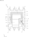
- FIG. 1 is a plan view showing a semiconductor device according to a first embodiment of the present disclosure
- FIG. FIG. 2 is a bottom view showing the semiconductor device according to the first embodiment of the present disclosure
- FIG. FIG. 3 is a main part plan view showing the semiconductor device according to the first embodiment of the present disclosure
- FIG. 4 is a cross-sectional view taken along line IV-IV of FIG.
- FIG. FIG. 7 is a cross-sectional view along line VII-VII of FIG.
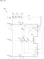
- FIG. 8 is a circuit section showing the semiconductor device according to the first embodiment of the present disclosure.
- FIG. 9 is a main part plan view showing a mounting structure of the semiconductor device according to the first embodiment of the present disclosure
- FIG. 10 is a cross-sectional view showing a first modification of the semiconductor device according to the first embodiment of the present disclosure
- FIG. 11 is an enlarged cross-sectional plan view of main parts showing a first modification of the semiconductor device according to the first embodiment of the present disclosure.
- FIG. 12 is a main part plan view showing a second modification of the semiconductor device according to the first embodiment of the present disclosure;
- FIG. 13 is a cross-sectional view showing a semiconductor device according to a second embodiment of the present disclosure;
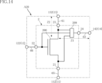
- FIG. 14 is a circuit section showing a semiconductor device according to a second embodiment of the present disclosure;
- FIG. 15 is a circuit section showing a semiconductor device according to a third embodiment of the present disclosure
- FIG. 16 is a main part plan view showing a mounting structure of a semiconductor device according to a fourth embodiment of the present disclosure
- 17 is a cross-sectional view along line XVII-XVII of FIG. 16.
- FIG. 18 is a circuit section showing a mounting structure of a semiconductor device according to a fourth embodiment of the present disclosure
- 19 is a plan view showing a semiconductor device according to a fifth embodiment of the present disclosure
- FIG. FIG. 20 is a main part plan view showing a mounting structure of a semiconductor device according to a fifth embodiment of the present disclosure
- 21 is a cross-sectional view taken along line XXI-XXI in FIG. 19.
- FIG. 19 is a cross-sectional view taken along line XXI-XXI in FIG. 19.
- FIG. 22 is a cross-sectional view along line XXII-XXII of FIG. 19.
- FIG. FIG. 23 is a plan view showing a semiconductor device according to a sixth embodiment of the present disclosure;
- FIG. 24 is a cross-sectional view along line XXIV-XXIV of FIG. 23.
- FIG. 25 is a cross-sectional view taken along line XXV--XXV of FIG. 23.
- a certain entity A is formed on a certain entity B” and “a certain entity A is formed on a certain entity B” mean “a certain entity A is formed on a certain entity B”. It includes "being directly formed in entity B” and “being formed in entity B while another entity is interposed between entity A and entity B”.
- ⁇ an entity A is placed on an entity B'' and ⁇ an entity A is located on an entity B'' mean ⁇ an entity A is located on an entity B.'' It includes "directly placed on B” and "some entity A is placed on an entity B while another entity is interposed between an entity A and an entity B.”
- ⁇ an object A is located on an object B'' means ⁇ an object A is adjacent to an object B and an object A is positioned on an object B. and "the thing A is positioned on the thing B while another thing is interposed between the thing A and the thing B".
- ⁇ an object A overlaps an object B when viewed in a certain direction'' means ⁇ an object A overlaps all of an object B'' and ⁇ an object A overlaps an object B.'' It includes "overlapping a part of a certain thing B".
- a certain surface A faces (one side or the other side of) direction B is not limited to the case where the angle of surface A with respect to direction B is 90 °, and the surface A Including when it is tilted against.
- First embodiment: 1 to 8 show a semiconductor device according to a first embodiment of the present disclosure.
- the semiconductor device A10 of this embodiment includes a first lead 11, a second lead 12, a third lead 13, a fourth lead 14, a semiconductor element 2, a first joint portion 61, a second joint portion 62, a plurality of wires 65, Wires 66 and sealing resin 7 are provided.
- FIG. 9 shows a mounting structure of a semiconductor device according to the first embodiment of the present disclosure.
- a semiconductor device mounting structure B10 of the present embodiment includes a semiconductor device A10 and a substrate 9 .
- FIG. 1 is a plan view showing the semiconductor device A10.
- FIG. 2 is a bottom view showing the semiconductor device A10.
- FIG. 3 is a fragmentary plan view showing the semiconductor device A10.
- FIG. 4 is a cross-sectional view taken along line IV-IV of FIG.
- FIG. 5 is a cross-sectional view along line VV of FIG. 6 is a cross-sectional view taken along line VI-VI of FIG. 3.
- FIG. FIG. 7 is a cross-sectional view along line VII-VII of FIG.
- FIG. 8 shows a circuit portion of the semiconductor device A10.
- FIG. 9 is a fragmentary plan view showing a mounting structure B10 for a semiconductor device.
- the z-direction is an example of the "thickness direction" and the y-direction is an example of the "first direction.”
- the semiconductor device A10 has a rectangular shape (or a substantially rectangular shape) when viewed in the z direction.
- the size of the semiconductor device A10 is not particularly limited. 0.5 mm to 1.5 mm.
- First lead 11, second lead 12, third lead 13, fourth lead 14 The first lead 11, the second lead 12, the third lead 13 and the fourth lead 14 are formed, for example, by punching or bending a metal plate. First lead 11, second lead 12, third lead 13 and fourth lead 14 are made of, for example, copper (Cu) or nickel (Ni), or an alloy thereof. Further, the first lead 11, the second lead 12, the third lead 13 and the fourth lead 14 may be provided with a plating layer at appropriate locations for the purpose of improving the wettability of solder or improving the bonding strength of wire bonding. good. The thickness of first lead 11, second lead 12, third lead 13 and fourth lead 14 is, for example, 0.1 mm to 0.3 mm.
- the arrangement of the first lead 11, the second lead 12, the third lead 13 and the fourth lead 14 is not limited at all. In the present embodiment, as shown in FIG. and the second lead 12 in the y direction.
- the fourth lead 14 is positioned between the first lead 11 and the second lead 12 and the third lead 13 in the y-direction.
- the first leads 11 and the second leads 12 are arranged in the x direction.
- the first lead 11, the second lead 12, the third lead 13 and the fourth lead 14 are arranged apart from each other when viewed in the z-direction.
- the third lead 13 and the fourth lead 14 are larger than the first lead 11 and the second lead 12 when viewed in the z direction.
- the second lead 12 has the smallest size when viewed in the z direction.
- the first lead 11 has a first bonding portion 114 and a plurality of (three in this embodiment) first extending portions 115 .
- the first bonding portion 114 is positioned on one side in the z direction (upper side in FIG. 4) with respect to the plurality of first extending portions 115 .
- the first bonding portion 114 is located inside the plurality of first extending portions 115 in the y direction.
- a plurality of first extending portions 115 extend from the first bonding portion 114 to the other side in the y direction. As viewed in the z-direction, the tip portion of the first extending portion 115 protrudes from the sealing resin 7 to the other side in the y-direction.
- the first lead 11 has a first main surface 111 and a first mounting surface 112 .
- the first main surface 111 is a surface facing one side in the z direction.
- the first mounting surface 112 is a surface facing the other side in the z direction.
- the first mounting surface 112 is a portion that is bonded with a bonding material such as solder when the semiconductor device A10 is mounted on the substrate 9 .
- the first lead 11 has a flat shape along the x-direction and the y-direction, but the specific shape of the first lead 11 is not limited at all. may
- the second lead 12 has a second bonding portion 124 and a second extending portion.
- the second bonding portion 124 is positioned on one side in the z direction (upper side in FIG. 5) with respect to the second extending portion 125 .
- the second bonding portion 124 is located inside the second extending portion 125 in the y direction.
- the second extending portion 125 extends from the second bonding portion 124 to the other side in the y direction.
- the tip portion of the second extending portion 125 protrudes from the sealing resin 7 to the other side in the y-direction.
- the second lead 12 has a second main surface 121 and a second mounting surface 122 .
- the second main surface 121 is a surface facing one side in the z direction.
- the second mounting surface 122 is a surface facing the other side in the z direction.
- the second mounting surface 122 is a portion that is bonded with a bonding material such as solder when the semiconductor device A10 is mounted on the substrate 9 .
- the second lead 12 has a flat shape along the x-direction and the y-direction, but the specific shape of the second lead 12 is not limited at all. may
- the third lead 13 has a third bonding portion 134 and a plurality of (four in this embodiment) third extending portions 135.
- the third bonding portion 134 has, for example, a rectangular shape when viewed in the z direction.
- a plurality of third extending portions 135 extend from the third bonding portion 134 to one side in the y direction.
- the tip portion of the third extending portion 135 protrudes from the sealing resin 7 to one side in the y-direction.
- the third lead 13 has a third main surface 131 and a third mounting surface 132 .
- the third main surface 131 is a surface facing one side in the z direction.
- the third mounting surface 132 is a surface facing the other side in the z direction.
- the third mounting surface 132 is a portion that is bonded with a bonding material such as solder when the semiconductor device A10 is mounted on the substrate 9 .
- the third lead 13 has a flat shape along the x-direction and the y-direction, but the specific shape of the third lead 13 is not limited at all. may
- the fourth lead 14 has a rectangular shape when viewed in the z direction, for example.
- the fourth lead 14 has a fourth major surface 141 and a fourth mounting surface 142 .
- the fourth main surface 141 is a surface facing one side in the z direction.
- the fourth mounting surface 142 is a surface facing the other side in the z direction.
- the fourth mounting surface 142 is a portion that is bonded with a bonding material when the semiconductor device A10 is mounted on the substrate 9 .
- the fourth lead 14 has a flat shape along the x-direction and the y-direction, but the specific shape of the fourth lead 14 is not limited at all. may
- the first mounting surface 112, the second mounting surface 122, the third mounting surface 132, and the fourth mounting surface 142 all have a shape along the xy plane and are flush with each other.
- the fact that the first mounting surface 112, the second mounting surface 122, the third mounting surface 132, and the fourth mounting surface 142 are flush is not limited to the case where the positions in the z-direction exactly match. This is a concept that includes deviations due to errors that are unavoidably included in processing.
- the semiconductor element 2 is an element that exerts an electrical function of the semiconductor device A10 and has a switching function.
- the type of the semiconductor element 2 is not particularly limited, and in this embodiment, the semiconductor element 2 is configured as a transistor (MOSFET). As shown in FIGS. 3 to 6, the semiconductor element 2 has an element body 20, a first electrode 21, a second electrode 22 and a third electrode .
- the element body 20 has a rectangular shape when viewed in the z direction.
- the element body 20 has an element main surface 201 and an element back surface 202 .
- the element main surface 201 and the element back surface 202 face opposite sides in the z direction.
- the element main surface 201 faces one side in the z direction.
- the element back surface 202 faces the other side in the z direction.
- a switching function unit 200 is built into the element body 20 .
- the switching function part 200 is a part including a semiconductor structure for realizing the switching function of the semiconductor element 2 . That is, the switching function unit 200 is provided with a channel in which, for example, an np junction and a pn junction are combined by adjoining an n-type semiconductor and a p-type semiconductor.
- the first electrode 21 and the second electrode 22 are arranged on the main surface 201 of the element.
- the third electrode 23 is arranged on the element back surface 202 .
- the constituent materials of the first electrode 21, the second electrode 22 and the third electrode 23 are not limited at all, and are, for example, copper (Cu), aluminum (Al), or alloys thereof.
- the first electrode 21 is the source electrode
- the second electrode 22 is the gate electrode
- the third electrode 23 is the drain electrode.
- the first electrode 21 covers most of the element principal surface 201 .
- the second electrode 22 is arranged at one corner (lower right corner in FIG. 3) of the element main surface 201 .
- the third electrode 23 covers the entire surface (or substantially the entire surface) of the element back surface 202 .
- the first joint portion 61 joins the third electrode 23 of the semiconductor element 2 and the third main surface 131 of the third lead 13, as shown in FIGS. In the present embodiment, a portion of the third electrode 23 on one side in the y direction is joined to the third main surface 131 of the third lead 13 by the first joining portion 61 .
- the first joint portion 61 is made of a conductive joint material such as solder, silver (Ag) paste, or silver (Ag) baking material.
- the first joint portion 61 is preferably a good conductor, and more preferably has a high thermal conductivity.
- the second joint portion 62 joins the third electrode 23 of the semiconductor element 2 and the fourth main surface 141 of the fourth lead 14, as shown in FIGS. In the present embodiment, a part of the third electrode 23 on the other side in the y direction is joined to the fourth main surface 141 of the fourth lead 14 by the second joining portion 62 .
- the second joint portion 62 includes a material with high impedance compared to good conductors such as silver (Ag) and copper (Cu). Moreover, it is preferable that the second joint portion 62 includes a material having a higher thermal conductivity than the resin or the like that constitutes the sealing resin 7, for example. Such materials include, for example, insulating high thermal conductive paste containing silicone or grease.
- high impedance in the present disclosure is a concept that includes substantially insulating properties.
- Another example of the material of the second joint portion 62 is an insulating high heat conductive sheet containing silicone or the like.
- the use of an insulating and highly thermally conductive sheet as the second joint 62 has the advantage that the thickness of the second joint 62 can be made more uniform.
- Wire 65: 3 and 4 the plurality of wires 65 are connected to the first electrodes 21 of the semiconductor element 2 and the first main surfaces 111 of the first leads 11 to connect the first electrodes 21 and the first leads 11 to each other. 11 are electrically connected.
- a specific configuration of the wire 65 is not limited at all, and it is, for example, a linear or belt-like conducting member containing gold (Au), aluminum (Al), copper (Cu), or the like. In the illustrated example, a strip-shaped wire 65 made of aluminum (Al) is used.
- Wire 66 The wire 66 is connected to the second electrode 22 of the semiconductor element 2 and the second main surface 121 of the second lead 12, as shown in FIGS. is conducting.
- a specific configuration of the wire 66 is not limited at all, and it is, for example, a linear or belt-like conducting member containing gold (Au), aluminum (Al), copper (Cu), or the like.
- a linear wire 65 made of gold (Au) is used.
- the encapsulating resin 7 includes parts of the first leads 11, the second leads 12, the third leads 13, and the fourth leads 14, the semiconductor element 2, the first joints 61, the second joints 62, and the plurality of wires. 65 and wires 66 are covered. Sealing resin 7 is made of, for example, black epoxy resin.
- the sealing resin 7 has a sealing resin main surface 71, a sealing resin back surface 72, and sealing resin side surfaces 73, 74, 75, and 76.
- the sealing resin main surface 71 and the sealing resin back surface 72 face opposite sides in the z direction.
- the sealing resin main surface 71 faces one side in the z direction.
- the sealing resin back surface 72 faces the other side in the z direction.
- the encapsulating resin side surface 73 is connected to the encapsulating resin main surface 71 and the encapsulating resin back surface 72 and faces one side in the x direction.
- the encapsulating resin side surface 74 is connected to the encapsulating resin main surface 71 and the encapsulating resin back surface 72 and faces the other side in the x direction.
- the encapsulating resin side surface 75 is connected to the encapsulating resin main surface 71 and the encapsulating resin back surface 72 and faces one side in the y direction.
- the encapsulating resin side surface 76 is connected to the encapsulating resin main surface 71 and the encapsulating resin back surface 72 and faces the other side in the y direction.
- a plurality of third extensions 135 protrude to one side in the y direction from the sealing resin side surface 75 .
- a plurality of first extensions 115 and second extensions 125 protrude to the other side in the y direction from the sealing resin side surface 76 .
- the first mounting surface 112 , the second mounting surface 122 , the third mounting surface 132 and the fourth mounting surface 142 are exposed from the sealing resin back surface 72 .
- the sealing resin back surface 72 and the first mounting surface 112, the second mounting surface 122, the third mounting surface 132, and the fourth mounting surface 142 are flush with each other.
- the third electrode 23 is connected to the third mounting surface 132 (the third lead 13) via the first joint portion 61, and the second joint It is connected to the fourth mounting surface 142 (the fourth lead 14) via the portion 62.
- FIG. A path from the switching function unit 200 to the fourth mounting surface 142 (fourth lead 14) includes the third electrode 23 and the second junction 62, and the impedance of this path is assumed to be impedance Z1.
- the path from the switching function unit 200 to the third mounting surface 132 (third lead 13) includes the third electrode 23 and the first joint 61, and the impedance of this path is assumed to be impedance Z2.
- the impedance Z1 is greater than the impedance Z2 due to the configuration of the second joint portion 62 described above.
- the first joint 61 contains a good conductor
- the second joint 62 contains the thermally conductive paste for successful insulation. to big.
- FIG. 9 shows a state in which the semiconductor device A10 is mounted on the substrate 9 in the semiconductor device mounting structure B10.
- the substrate 9 has an insulating portion 91 and a wiring portion 92 .
- Insulating portion 91 is made of an insulating material such as epoxy resin or ceramics.
- the wiring portion 92 is made of a conductor such as copper (Cu) or nickel (Ni) formed on the surface of or inside the insulating portion 91 .
- the wiring portion 92 includes a first area 921 , a second area 922 , a third area 923 and a fourth area 924 . In this embodiment, the first area 921 , the second area 922 , the third area 923 and the fourth area 924 are arranged on one side of the insulating portion 91 .
- the first region 921 is conductively joined to the first mounting surface 112 of the first lead 11 by soldering or the like.
- the first region 921 is electrically connected to a terminal (not shown) through which a main current for switching the semiconductor element 2 is input/output.
- the second mounting surface 122 of the second lead 12 is conductively joined to the second region 922 by soldering or the like.
- the second region 922 is electrically connected to a terminal (not shown) to which a control signal for controlling the switching function of the semiconductor element 2 is input.
- the third mounting surface 132 of the third lead 13 is conductively joined to the third region 923 by soldering or the like.
- the third region 923 is electrically connected to another terminal (not shown) through which the main current for switching the semiconductor element 2 is input/output.
- the fourth area 924 is conductively joined to the fourth mounting surface 142 of the fourth lead 14 by soldering or the like.
- the fourth region 924 is electrically connected to a ground line (not shown).
- the third electrode 23 arranged on the element back surface 202 of the element body 20 is joined to the third lead 13 and the fourth lead 14 .
- heat generated in the semiconductor element 2 (element body 20) during operation of the semiconductor device A10 can be dissipated to the outside through the third lead 13 and the fourth lead .
- impedance Z1 is greater than impedance Z2. Therefore, it is possible to prevent the current flowing through the third lead 13 from flowing from the fourth lead 14 to the outside.
- electromagnetic noise can be suppressed from being emitted from the fourth region 924 or the like to which the fourth lead 14 is joined. Therefore, according to the present embodiment, it is possible to promote heat dissipation and suppress noise.
- the second joint portion 62 contains an insulating high thermal conductive paste, the second joint portion 62 has higher thermal conductivity than the sealing resin 7, for example. Therefore, heat dissipation from the semiconductor element 2 (element body 20) to the fourth lead 14 can be promoted.
- each part in each modified example and each embodiment can be appropriately combined with each other within a range that does not cause technical contradiction.
- the second joint portion 62 containing the insulating high thermal conductive paste has high insulating properties. Therefore, the impedance Z1 can be significantly higher than the impedance Z2. Therefore, it is preferable to promote heat dissipation and suppress noise.
- the fourth lead 14 is conductively joined to the fourth region 924 .
- the fourth region 924 is grounded to a ground line (not shown). Thereby, the fourth lead 14 can be electrically stabilized.
- the size of the fourth lead 14 is larger than the first lead 11 and the second lead 12. This is advantageous for promoting heat dissipation.
- First modification: 10 and 11 show a first modification of the semiconductor device A10.
- the semiconductor device A11 of this modified example differs from the example described above in the configuration of the second joint portion 62 .
- the second joint 62 of this example includes an insulating layer 621 , a metal layer 622 and a metal layer 623 .
- the insulating layer 621 is a plate-shaped member made of ceramic such as alumina (Al 2 O 3 ), aluminum nitride (AlN), silicon nitride (SiN), or the like.
- the metal layer 622 is formed on one side (the side facing one side in the z direction) of the insulating layer 621 and contains copper (Cu), for example.
- the metal layer 623 is formed on one side (the side facing the other side in the z direction) of the insulating layer 621 and contains copper (Cu), for example.
- Such insulating layer 621, metal layer 622 and metal layer 623 constitute, for example, a DBC (Direct Bonded Copper) substrate.
- the second joint portion 62 of this example further includes a conductive joint material 624 and a conductive joint material 625 .
- the conductive bonding material 624 bonds the third electrode 23 of the semiconductor element 2 and the metal layer 622 .
- a conductive bonding material 625 bonds the fourth main surface 141 of the fourth lead 14 and the metal layer 623 .
- Conductive bonding material 624 and conductive bonding material 625 are, for example, solder, silver (Ag) paste, silver (Ag) sintered material, or the like.
- the second joint portion 62 has the insulating layer 621 to join the third electrode 23 of the semiconductor element 2 and the fourth main surface 141 of the fourth lead 14 and insulate them.
- This modification can also promote heat dissipation and suppress noise.
- the specific configuration of the second joint portion 62 is not limited at all.
- the second joint portion 62 using the DBC substrate has the advantage of being less susceptible to damage due to heat cycle loads.
- FIG. 12 shows a second modification of the semiconductor device A10.
- the semiconductor device A12 of this example includes conductive members 67 in place of the plurality of wires 65 of the above example.
- the conductive member 67 is formed by cutting and bending a plate-shaped member made of metal such as copper (Cu).
- the conductive member 67 has a bent shape, for example, when viewed along the x direction.
- the conductive member 67 is electrically connected to the first electrode 21 of the semiconductor element 2 and the first main surface 111 of the first lead 11 .
- This modification can also promote heat dissipation and suppress noise.
- the specific configuration for electrically connecting the first electrode 21 and the first lead 11 is not limited at all.
- Second embodiment 13 and 14 show a semiconductor device according to a second embodiment of the present disclosure.
- the semiconductor device A20 of this embodiment differs from the above-described embodiments in the configuration of the semiconductor element 2 and the bonding form between the semiconductor element 2 and the fourth lead 14 .
- the semiconductor element 2 of this modified example has an element insulating layer 209 and a fourth electrode 24 .
- the element insulating layer 209 is provided on part of the element back surface 202 of the element body 20 .
- the element insulating layer 209 is arranged at a position avoiding the third electrode 23 when viewed in the z direction, and is positioned on the other side of the third electrode 23 in the y direction in the illustrated example.
- a fourth electrode 24 is formed on the element insulating layer 209 . That is, the element insulating layer 209 is interposed between the element body 20 and the fourth electrode 24 .
- Device insulating layer 209 includes an insulating material such as silicon dioxide (SiO 2 ) or silicon nitride (SiN). Due to the presence of the element insulating layer 209, the fourth electrode 24 is insulated from the switching function section 200 (element body 20). Also, the fourth electrode 24 is insulated from the first electrode 21 , the second electrode 22 and the third electrode 23 .
- the fourth electrode 24 is joined to the fourth main surface 141 of the fourth lead 14 by the third joint portion 63 .
- Solder, silver (Ag) paste, silver (Ag) firing material, or the like, for example, is selected as the material of the third joint portion 63 .
- the path from the switching function part 200 to the fourth mounting surface 142 (fourth lead 14) includes an element insulating layer 209.
- the impedance Z1 is larger than the impedance Z2.
- the impedance Z1 is large enough to be recognized as infinite (insulating) compared to the impedance Z2.
- the device insulating layer 209 exhibits good insulating properties even if it is very thin. Therefore, it is possible to conduct heat more efficiently from the element main body 20 to the fourth lead 14, which is preferable for promoting heat dissipation. Moreover, it is advantageous for increasing the impedance Z1.
- FIG. 15 shows a semiconductor device according to a third embodiment of the present disclosure.
- the semiconductor device A30 of this embodiment differs from the above-described embodiments in the configuration of the semiconductor element 2, and other configurations are similar to, for example, the semiconductor device A20.
- the semiconductor element 2 of this embodiment has an insulating element portion 28 .
- the insulating element section 28 functions to insulate the fourth electrode 24 and the switching function section 200 .
- the isolation element portion 28 includes diodes 281 and 282 .
- Diodes 281 and 282 are connected in series and have polarities opposite to each other. For this reason. Diodes 281 and 282 perform an isolation function to prevent conduction.
- the specific configuration of the insulating element portion 28 is not limited at all, and is built into a part of the element main body 20, for example.
- a semiconductor device mounting structure B40 of this embodiment includes a semiconductor device A40 and a substrate 9 .
- the semiconductor device A40 has the first lead 11, the second lead 12 and the third lead 13, and does not have the fourth lead 14 described above.
- the semiconductor element 2 has an element body 20 (including a switching function section 200), a first electrode 21, a second electrode 22 and a third electrode 23, and has the element insulating layer 209 and the insulating element section 28 described above. not.
- the third electrode 23 is electrically connected in its entirety to the third main surface 131 of the third lead 13 by the first joint portion 61 .
- the wiring portion 92 of the substrate 9 of this embodiment includes a first area 921, a second area 922, a third area 923, a fourth area 924, a fifth area 925 and a sixth area. 926 , a first terminal 931 , a second terminal 932 , a third terminal 933 and a ground terminal 934 .
- the first mounting surface 112 of the first lead 11 is joined to the first region 921 via a conductive joint 81 such as solder.
- the second mounting surface 122 of the second lead 12 is joined to the second region 922 via a conductive joint 82 such as solder.
- Part of the third mounting surface 132 of the third lead 13 is joined to the third region 923 via a conductive joint 83 such as solder.
- Another part of the third mounting surface 132 of the third lead 13 is joined to the fourth region 924 via a conductive joint 84 such as solder.
- the first area 921, the second area 922, the third area 923, and the fourth area 924 are arranged as shown in FIG. 16, and are similar to the configuration described with reference to FIG.
- the fifth region 925 is made of, for example, a metal layer built into the insulating portion 91 .
- the fifth region 925 is electrically connected to the ground terminal 934 .
- the ground terminal 934 is a terminal grounded by being connected to a ground line (not shown) outside the substrate 9 .
- the sixth region 926 is electrically interposed between the fourth region 924 and the fifth region 925.
- the specific configuration of the sixth region 926 is not limited at all, and in this example, it is configured by a via that connects the fourth region 924 and the fifth region 925 in the z direction.
- the constituent material of sixth region 926 includes a material having higher impedance than, for example, copper (Cu), nickel (Ni), or the like constituting other portions of wiring portion 92 .
- Examples of the material of the sixth region 926 include a high heat conductive resin containing polycarbonate, polyethylene terephthalate, polyamide, etc., which fills the through holes provided in the insulating portion 91 .
- a through-hole conductive portion including a conductive portion such as a metal and a high heat conductive sheet interposed between the through-hole conductive portion and the fourth region 924 or the fifth region 925 may be combined. good.
- the first region 921 is electrically connected to the first terminal 931.
- the first terminal 931 is a terminal to which a main current for switching the semiconductor element 2 is input/output.
- the second region 922 is electrically connected to the second terminal 932 .
- the second terminal 932 is a terminal to which a control signal for controlling the switching function of the semiconductor element 2 is input.
- the third region 923 is electrically connected to the third terminal 933 .
- the third terminal 933 is another terminal to which the main current for switching the semiconductor element 2 is input/output.
- the specific configurations of the first terminal 931, the second terminal 932, the third terminal 933 and the ground terminal 934 are not limited at all.
- the first terminal 931, the second terminal 932, the third terminal 933, and the ground terminal 934 may be connectors to which connectors or the like outside the substrate 9 are connected, or mounting terminal portions.
- the first terminal 931, the second terminal 932, the third terminal 933, and the ground terminal 934 may be part of the wiring section 92 on which other electronic components are mounted (conductively joined).
- the impedance Z3 of the path from the third lead 13 to the fifth area 925 via the fourth area 924 and the sixth area 926 is the impedance Z4 of the path from the third lead 13 to the third terminal 933 via the third area 923. bigger than This is because the sixth region 926 contains the high impedance material described above.
- Fifth embodiment 19 to 22 show a semiconductor device A50 and a semiconductor device mounting structure B50 according to the fifth embodiment of the present disclosure.
- the semiconductor device A50 of this embodiment includes a fifth lead 15, and other configurations are similar to those of the semiconductor device A10, for example.
- the fifth lead 15 is made of the same material as the first lead 11, second lead 12, third lead 13 and fourth lead 14.
- the fifth lead 15 has a main portion 154 and two extension portions 155 .
- the main portion 154 is located on one side of the semiconductor element 2 in the z direction.
- the main portion 154 overlaps the entire semiconductor element 2 when viewed in the z direction.
- the main portion 154 is rectangular.
- a sealing resin 7 is interposed between the main portion 154 and the semiconductor element 2 and the wires 65 and 66 .
- a surface facing one side in the z direction of the main portion 154 is the fifth main surface 151 .
- the two extending portions 155 extend from the main portion 154 to both sides in the x direction.
- the extending portion 155 has a first portion 1551 , a second portion 1552 and a third portion 1553 .
- the first portion 1551 is a straight portion extending from the main portion 154 in the x direction.
- the second part 1552 is located outside the first part 1551 in the x direction and on the other side in the z direction.
- the second portion 1552 has a fifth mounting surface 152 .
- the fifth mounting surface 152 is flush with the first mounting surface 112 , the second mounting surface 122 , the third mounting surface 132 and the fourth mounting surface 142 .
- the third portion 1553 connects the first portion 1551 and the second portion 1552 and has a shape along the z direction, for example.
- the wiring portion 92 of the substrate 9 of this embodiment has two seventh regions 927. As shown in FIG. The two seventh regions 927 are arranged separately on both sides of the fourth region 924 in the x direction.
- the seventh region 927 is electrically connected to, for example, a ground line (not shown).
- the fifth mounting surfaces 152 of the two extensions 155 of the fifth lead 15 are individually conductively joined to the two seventh regions 927 via conductive joints 87 such as solder.
- the fifth lead 15 can shield electromagnetic noise emitted from the semiconductor element 2 to one side in the z direction. Thereby, noise can be suppressed more. By grounding the fifth lead 15 through the seventh region 927, noise can be shielded more efficiently.
- Sixth embodiment 23 to 25 show a semiconductor device and a mounting structure of the semiconductor device according to the sixth embodiment of the present disclosure.
- substrate 9 is added and shown for convenience of an understanding.
- the semiconductor device A60 of this embodiment includes the fifth lead 15 described above. Other configurations are similar to those of the semiconductor device A40 described above. That is, the semiconductor device A60 does not employ a configuration that intentionally forms a path with high impedance.
- the substrate 9 of this embodiment has the same configuration as the substrate 9 of the mounting structure B50 of the semiconductor device described above. That is, the fifth lead 15 of the semiconductor device A60 is grounded to a ground line (not shown) through the seventh region 927 of the substrate 9.
- FIG. 1 A ground line (not shown) through the seventh region 927 of the substrate 9.
- the semiconductor device and the mounting structure of the semiconductor device according to the present disclosure are not limited to the above-described embodiments.
- the specific configuration of each part of the semiconductor device and the mounting structure of the semiconductor device according to the present disclosure can be changed in various ways.
- the present disclosure includes embodiments set forth in the following appendices.
- Appendix 1 It has a first electrode and a second electrode located on one side in the thickness direction, and a third electrode located on the other side in the thickness direction, and the first electrode is controlled by the state of voltage application to the second electrode.
- Appendix 2 a first joint that joins the third electrode and the third lead; a second joint that joins the third electrode and the fourth lead, The semiconductor device according to appendix 1, wherein the impedance of the second junction is higher than the impedance of the first junction.
- Appendix 3 The semiconductor device according to appendix 2, wherein the first junction includes metal.
- Appendix 4. 3.
- Appendix 5. 3. The semiconductor device according to appendix 3, wherein the second joint includes ceramics. Appendix 6.
- the semiconductor element includes: an element body in which the first electrode and the second electrode are arranged on one side in the thickness direction and the third electrode is arranged on the other side in the thickness direction; a fourth electrode arranged on the other side in the thickness direction; the fourth electrode and the fourth lead are joined together,
- the semiconductor device according to appendix 1 wherein impedance of a path from the switching function unit to the fourth electrode is higher than impedance from the switching function unit to the third electrode.
- Appendix 7. 7.
- the third lead has a third mounting surface facing the other side in the thickness direction and exposed from the sealing resin;
- the first lead has a first mounting surface facing the other side in the thickness direction and exposed from the sealing resin;
- the second lead has a second mounting surface facing the other side in the thickness direction and exposed from the sealing resin;
- the fourth lead has a fourth mounting surface facing the other side in the thickness direction and exposed from the sealing resin;
- a semiconductor element having a first electrode, a second electrode, and a third electrode, wherein an energization state of the first electrode and the second electrode is controlled by a voltage application state to the second electrode; a first lead electrically connected to the first electrode; a second lead electrically connected to the second electrode; a third lead electrically connected to the third electrode; a semiconductor device comprising: a sealing resin covering at least the semiconductor element; a substrate on which the semiconductor device is mounted; The substrate includes an insulating portion and a wiring portion, The wiring portion includes a first region conductively joined to the first lead, a second region conductively joined to the second lead, a third region conductively joined to the third lead, and adjacent to the third region.
- a fourth region connected to and conductively joined to the third lead, a ground-connected fifth region, a sixth region electrically interposed between the fourth region and the fifth region, and the third region including a main current terminal conducting to The impedance of the path from the third lead to the fifth area via the fourth area and the sixth area is higher than the impedance of the path from the third lead to the main current terminal.
- the fourth region and the fifth region are arranged apart in the thickness direction of the substrate, 18.
- A10, A11, A12, A20 Semiconductor devices A30, A40, A50, A60: Semiconductor devices B10, B40, B50: Mounting structures Z1, Z2, Z3, Z4: Impedance 2: Semiconductor element 7: Sealing resin 9: Substrate 11: first lead 12: second lead 13: third lead 14: fourth lead 15: fifth lead 20: element body 21: first electrode 22: second electrode 23: third electrode 24: fourth electrode : insulating element portion 61: first joint portion 62: second joint portion 63: third joint portion 65, 66: wire 67: conduction member 71: sealing resin main surface 72: sealing resin rear surface 73, 74, 75, 76: sealing resin side surfaces 81, 82, 83, 84, 87: conductive joint portion 91: insulating portion 92: wiring portion 111: first main surface 112: first mounting surface 114: first bonding portion 115: first first Extension 121: Second main surface 122: Second mounting surface 124: Second bonding
Landscapes
- Structures Or Materials For Encapsulating Or Coating Semiconductor Devices Or Solid State Devices (AREA)
- Engineering & Computer Science (AREA)
- Microelectronics & Electronic Packaging (AREA)
Priority Applications (2)
| Application Number | Priority Date | Filing Date | Title |
|---|---|---|---|
| JP2024501060A JPWO2023157604A1 (https=) | 2022-02-15 | 2023-01-27 | |
| US18/796,813 US20240404941A1 (en) | 2022-02-15 | 2024-08-07 | Semiconductor device and package structure of semiconductor device |
Applications Claiming Priority (2)
| Application Number | Priority Date | Filing Date | Title |
|---|---|---|---|
| JP2022-021567 | 2022-02-15 | ||
| JP2022021567 | 2022-02-15 |
Related Child Applications (1)
| Application Number | Title | Priority Date | Filing Date |
|---|---|---|---|
| US18/796,813 Continuation US20240404941A1 (en) | 2022-02-15 | 2024-08-07 | Semiconductor device and package structure of semiconductor device |
Publications (1)
| Publication Number | Publication Date |
|---|---|
| WO2023157604A1 true WO2023157604A1 (ja) | 2023-08-24 |
Family
ID=87578390
Family Applications (1)
| Application Number | Title | Priority Date | Filing Date |
|---|---|---|---|
| PCT/JP2023/002555 Ceased WO2023157604A1 (ja) | 2022-02-15 | 2023-01-27 | 半導体装置および半導体装置の実装構造体 |
Country Status (3)
| Country | Link |
|---|---|
| US (1) | US20240404941A1 (https=) |
| JP (1) | JPWO2023157604A1 (https=) |
| WO (1) | WO2023157604A1 (https=) |
Citations (6)
| Publication number | Priority date | Publication date | Assignee | Title |
|---|---|---|---|---|
| JPH0870059A (ja) * | 1994-08-16 | 1996-03-12 | Samsung Electron Co Ltd | 分離されたダイパッドを有する半導体パッケージ |
| JPH1098150A (ja) * | 1996-09-25 | 1998-04-14 | Nec Corp | モールド型半導体装置 |
| JP2002009222A (ja) * | 2000-06-19 | 2002-01-11 | Oki Electric Ind Co Ltd | 樹脂封止型半導体装置 |
| JP2002009219A (ja) * | 2000-06-22 | 2002-01-11 | Toshiba Corp | 樹脂封止型半導体装置 |
| JP2007157862A (ja) * | 2005-12-02 | 2007-06-21 | Fuji Electric Device Technology Co Ltd | 半導体装置 |
| JP2015097237A (ja) * | 2013-11-15 | 2015-05-21 | 住友電気工業株式会社 | 半導体装置 |
-
2023
- 2023-01-27 JP JP2024501060A patent/JPWO2023157604A1/ja active Pending
- 2023-01-27 WO PCT/JP2023/002555 patent/WO2023157604A1/ja not_active Ceased
-
2024
- 2024-08-07 US US18/796,813 patent/US20240404941A1/en active Pending
Patent Citations (6)
| Publication number | Priority date | Publication date | Assignee | Title |
|---|---|---|---|---|
| JPH0870059A (ja) * | 1994-08-16 | 1996-03-12 | Samsung Electron Co Ltd | 分離されたダイパッドを有する半導体パッケージ |
| JPH1098150A (ja) * | 1996-09-25 | 1998-04-14 | Nec Corp | モールド型半導体装置 |
| JP2002009222A (ja) * | 2000-06-19 | 2002-01-11 | Oki Electric Ind Co Ltd | 樹脂封止型半導体装置 |
| JP2002009219A (ja) * | 2000-06-22 | 2002-01-11 | Toshiba Corp | 樹脂封止型半導体装置 |
| JP2007157862A (ja) * | 2005-12-02 | 2007-06-21 | Fuji Electric Device Technology Co Ltd | 半導体装置 |
| JP2015097237A (ja) * | 2013-11-15 | 2015-05-21 | 住友電気工業株式会社 | 半導体装置 |
Also Published As
| Publication number | Publication date |
|---|---|
| JPWO2023157604A1 (https=) | 2023-08-24 |
| US20240404941A1 (en) | 2024-12-05 |
Similar Documents
| Publication | Publication Date | Title |
|---|---|---|
| JP7137558B2 (ja) | 半導体装置 | |
| KR100284241B1 (ko) | 반도체장치 | |
| JP6726112B2 (ja) | 半導体装置および電力変換装置 | |
| TWI801237B (zh) | 功率封裝模組 | |
| KR101614669B1 (ko) | 전력용 반도체 장치 | |
| US20080029875A1 (en) | Hermetically sealed semiconductor device module | |
| JP6604926B2 (ja) | 半導体モジュール | |
| WO2021200336A1 (ja) | 電子装置 | |
| WO2021251126A1 (ja) | 半導体装置 | |
| JP7204174B2 (ja) | 半導体装置及び半導体装置の製造方法 | |
| CN118805253A (zh) | 半导体装置以及半导体模块 | |
| KR20170024254A (ko) | 파워 반도체 모듈 및 이의 제조 방법 | |
| JP7608903B2 (ja) | 半導体装置 | |
| US20240244750A1 (en) | Semiconductor module | |
| WO2023157604A1 (ja) | 半導体装置および半導体装置の実装構造体 | |
| US20230087499A1 (en) | Semiconductor unit and semiconductor device | |
| CN117080175A (zh) | 功率封装模块 | |
| WO2021241304A1 (ja) | 半導体モジュールの実装構造 | |
| US12463119B2 (en) | Semiconductor device and semiconductor device manufacturing method | |
| US20250329628A1 (en) | Semiconductor device | |
| US20240413049A1 (en) | Semiconductor device | |
| WO2023199808A1 (ja) | 半導体装置 | |
| WO2026042545A1 (ja) | 半導体装置 | |
| WO2025182584A1 (ja) | 半導体装置 | |
| WO2024128062A1 (ja) | 半導体装置 |
Legal Events
| Date | Code | Title | Description |
|---|---|---|---|
| 121 | Ep: the epo has been informed by wipo that ep was designated in this application |
Ref document number: 23756132 Country of ref document: EP Kind code of ref document: A1 |
|
| WWE | Wipo information: entry into national phase |
Ref document number: 2024501060 Country of ref document: JP |
|
| NENP | Non-entry into the national phase |
Ref country code: DE |
|
| 122 | Ep: pct application non-entry in european phase |
Ref document number: 23756132 Country of ref document: EP Kind code of ref document: A1 |