WO2023157566A1 - 処理方法及び処理システム - Google Patents
処理方法及び処理システム Download PDFInfo
- Publication number
- WO2023157566A1 WO2023157566A1 PCT/JP2023/001867 JP2023001867W WO2023157566A1 WO 2023157566 A1 WO2023157566 A1 WO 2023157566A1 JP 2023001867 W JP2023001867 W JP 2023001867W WO 2023157566 A1 WO2023157566 A1 WO 2023157566A1
- Authority
- WO
- WIPO (PCT)
- Prior art keywords
- substrate
- wafer
- interface
- amount
- peripheral
- Prior art date
- Legal status (The legal status is an assumption and is not a legal conclusion. Google has not performed a legal analysis and makes no representation as to the accuracy of the status listed.)
- Ceased
Links
Images







Classifications
-
- B—PERFORMING OPERATIONS; TRANSPORTING
- B23—MACHINE TOOLS; METAL-WORKING NOT OTHERWISE PROVIDED FOR
- B23K—SOLDERING OR UNSOLDERING; WELDING; CLADDING OR PLATING BY SOLDERING OR WELDING; CUTTING BY APPLYING HEAT LOCALLY, e.g. FLAME CUTTING; WORKING BY LASER BEAM
- B23K26/00—Working by laser beam, e.g. welding, cutting or boring
- B23K26/50—Working by transmitting the laser beam through or within the workpiece
- B23K26/53—Working by transmitting the laser beam through or within the workpiece for modifying or reforming the material inside the workpiece, e.g. for producing break initiation cracks
-
- B—PERFORMING OPERATIONS; TRANSPORTING
- B23—MACHINE TOOLS; METAL-WORKING NOT OTHERWISE PROVIDED FOR
- B23K—SOLDERING OR UNSOLDERING; WELDING; CLADDING OR PLATING BY SOLDERING OR WELDING; CUTTING BY APPLYING HEAT LOCALLY, e.g. FLAME CUTTING; WORKING BY LASER BEAM
- B23K26/00—Working by laser beam, e.g. welding, cutting or boring
- B23K26/0006—Working by laser beam, e.g. welding, cutting or boring taking account of the properties of the material involved
-
- B—PERFORMING OPERATIONS; TRANSPORTING
- B23—MACHINE TOOLS; METAL-WORKING NOT OTHERWISE PROVIDED FOR
- B23K—SOLDERING OR UNSOLDERING; WELDING; CLADDING OR PLATING BY SOLDERING OR WELDING; CUTTING BY APPLYING HEAT LOCALLY, e.g. FLAME CUTTING; WORKING BY LASER BEAM
- B23K26/00—Working by laser beam, e.g. welding, cutting or boring
- B23K26/02—Positioning or observing the workpiece, e.g. with respect to the point of impact; Aligning, aiming or focusing the laser beam
- B23K26/03—Observing, e.g. monitoring, the workpiece
- B23K26/032—Observing, e.g. monitoring, the workpiece using optical means
-
- B—PERFORMING OPERATIONS; TRANSPORTING
- B23—MACHINE TOOLS; METAL-WORKING NOT OTHERWISE PROVIDED FOR
- B23K—SOLDERING OR UNSOLDERING; WELDING; CLADDING OR PLATING BY SOLDERING OR WELDING; CUTTING BY APPLYING HEAT LOCALLY, e.g. FLAME CUTTING; WORKING BY LASER BEAM
- B23K26/00—Working by laser beam, e.g. welding, cutting or boring
- B23K26/02—Positioning or observing the workpiece, e.g. with respect to the point of impact; Aligning, aiming or focusing the laser beam
- B23K26/04—Automatically aligning, aiming or focusing the laser beam, e.g. using the back-scattered light
- B23K26/042—Automatically aligning the laser beam
-
- B—PERFORMING OPERATIONS; TRANSPORTING
- B23—MACHINE TOOLS; METAL-WORKING NOT OTHERWISE PROVIDED FOR
- B23K—SOLDERING OR UNSOLDERING; WELDING; CLADDING OR PLATING BY SOLDERING OR WELDING; CUTTING BY APPLYING HEAT LOCALLY, e.g. FLAME CUTTING; WORKING BY LASER BEAM
- B23K26/00—Working by laser beam, e.g. welding, cutting or boring
- B23K26/36—Removing material
- B23K26/40—Removing material taking account of the properties of the material involved
- B23K26/402—Removing material taking account of the properties of the material involved involving non-metallic material, e.g. isolators
-
- H—ELECTRICITY
- H10—SEMICONDUCTOR DEVICES; ELECTRIC SOLID-STATE DEVICES NOT OTHERWISE PROVIDED FOR
- H10P—GENERIC PROCESSES OR APPARATUS FOR THE MANUFACTURE OR TREATMENT OF DEVICES COVERED BY CLASS H10
- H10P10/00—Bonding of wafers, substrates or parts of devices
- H10P10/12—Bonding of semiconductor wafers or semiconductor substrates to semiconductor wafers or semiconductor substrates
-
- H—ELECTRICITY
- H10—SEMICONDUCTOR DEVICES; ELECTRIC SOLID-STATE DEVICES NOT OTHERWISE PROVIDED FOR
- H10P—GENERIC PROCESSES OR APPARATUS FOR THE MANUFACTURE OR TREATMENT OF DEVICES COVERED BY CLASS H10
- H10P52/00—Grinding, lapping or polishing of wafers, substrates or parts of devices
-
- H—ELECTRICITY
- H10—SEMICONDUCTOR DEVICES; ELECTRIC SOLID-STATE DEVICES NOT OTHERWISE PROVIDED FOR
- H10P—GENERIC PROCESSES OR APPARATUS FOR THE MANUFACTURE OR TREATMENT OF DEVICES COVERED BY CLASS H10
- H10P72/00—Handling or holding of wafers, substrates or devices during manufacture or treatment thereof
- H10P72/04—Apparatus for manufacture or treatment
- H10P72/0428—Apparatus for mechanical treatment or grinding or cutting
-
- H—ELECTRICITY
- H10—SEMICONDUCTOR DEVICES; ELECTRIC SOLID-STATE DEVICES NOT OTHERWISE PROVIDED FOR
- H10P—GENERIC PROCESSES OR APPARATUS FOR THE MANUFACTURE OR TREATMENT OF DEVICES COVERED BY CLASS H10
- H10P72/00—Handling or holding of wafers, substrates or devices during manufacture or treatment thereof
- H10P72/06—Apparatus for monitoring, sorting, marking, testing or measuring
- H10P72/0606—Position monitoring, e.g. misposition detection or presence detection
-
- H—ELECTRICITY
- H10—SEMICONDUCTOR DEVICES; ELECTRIC SOLID-STATE DEVICES NOT OTHERWISE PROVIDED FOR
- H10P—GENERIC PROCESSES OR APPARATUS FOR THE MANUFACTURE OR TREATMENT OF DEVICES COVERED BY CLASS H10
- H10P72/00—Handling or holding of wafers, substrates or devices during manufacture or treatment thereof
- H10P72/50—Handling or holding of wafers, substrates or devices during manufacture or treatment thereof for positioning, orientation or alignment
- H10P72/53—Handling or holding of wafers, substrates or devices during manufacture or treatment thereof for positioning, orientation or alignment using optical controlling means
-
- H—ELECTRICITY
- H10—SEMICONDUCTOR DEVICES; ELECTRIC SOLID-STATE DEVICES NOT OTHERWISE PROVIDED FOR
- H10P—GENERIC PROCESSES OR APPARATUS FOR THE MANUFACTURE OR TREATMENT OF DEVICES COVERED BY CLASS H10
- H10P72/00—Handling or holding of wafers, substrates or devices during manufacture or treatment thereof
- H10P72/70—Handling or holding of wafers, substrates or devices during manufacture or treatment thereof for supporting or gripping
-
- H—ELECTRICITY
- H10—SEMICONDUCTOR DEVICES; ELECTRIC SOLID-STATE DEVICES NOT OTHERWISE PROVIDED FOR
- H10P—GENERIC PROCESSES OR APPARATUS FOR THE MANUFACTURE OR TREATMENT OF DEVICES COVERED BY CLASS H10
- H10P95/00—Generic processes or apparatus for manufacture or treatments not covered by the other groups of this subclass
-
- B—PERFORMING OPERATIONS; TRANSPORTING
- B23—MACHINE TOOLS; METAL-WORKING NOT OTHERWISE PROVIDED FOR
- B23K—SOLDERING OR UNSOLDERING; WELDING; CLADDING OR PLATING BY SOLDERING OR WELDING; CUTTING BY APPLYING HEAT LOCALLY, e.g. FLAME CUTTING; WORKING BY LASER BEAM
- B23K2101/00—Articles made by soldering, welding or cutting
- B23K2101/36—Electric or electronic devices
- B23K2101/40—Semiconductor devices
Definitions
- the present disclosure relates to processing methods and processing systems.
- Patent Document 1 in a superimposed substrate in which a first substrate and a second substrate are bonded, a reforming agent is introduced into the inside of the first substrate along the boundary between the peripheral edge portion and the central portion of the first substrate to be removed.
- a substrate processing system includes a modified layer forming device for forming a layer and a peripheral edge removing device for removing a peripheral edge portion of a first substrate with the modified layer as a starting point.
- the technique according to the present disclosure appropriately removes the peripheral portion of the first substrate in the superimposed substrate in which the first substrate and the second substrate are bonded.
- One aspect of the present disclosure is a method of processing a superimposed substrate in which a first substrate and a second substrate are bonded together, comprising obtaining an eccentricity amount of the first substrate and the second substrate; irradiating an internal laser beam along the boundary between the peripheral edge portion of the substrate and the central portion of the first substrate to form a peripheral edge modified layer that serves as a starting point for peeling of the peripheral edge portion; and removing the peripheral portion with the modified layer as a base point, and determining an irradiation position of the internal laser beam based on the amount of eccentricity when forming the peripheral modified layer.
- the peripheral portion of the first substrate can be appropriately removed.
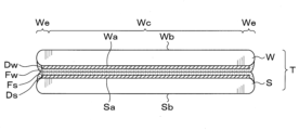
- FIG. 3 is a side view showing a configuration example of a superimposed wafer to be processed
- 1 is a plan view showing an outline of the configuration of a wafer processing system according to this embodiment
- FIG. FIG. 10 is a cross section showing states of a bonding strength decreased region, a peripheral modified layer, and a split modified layer formed on a superposed wafer
- FIG. FIG. 2 is a side view showing the schematic configuration of an interfacial reforming device and an internal reforming device
- FIG. 5 is an explanatory diagram showing how a deviation amount detection unit operates
- FIG. 10 is an explanatory diagram showing another arrangement example of the displacement amount detection unit
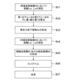
- FIG. 4 is a side view showing another configuration example of the interfacial reforming device and the internal reforming device; 4 is a flow chart showing main steps of wafer processing in the wafer processing system;
- FIG. 10 is an explanatory diagram showing an example of a measurement result by a displacement amount detection unit;
- FIG. 3 is an explanatory diagram showing main steps of wafer processing in the wafer processing system;
- FIG. 4 is a side view showing another configuration example of the interfacial reforming device and the internal reforming device;
- FIG. 11 is an explanatory diagram showing another example of formation of a bonding strength decrease region; It is explanatory drawing which shows the other example of formation of a peripheral modified layer. It is explanatory drawing which shows the other example of formation of a peripheral modification layer.
- FIG. 10 is an explanatory diagram showing another step of wafer processing in the wafer processing system;
- a first substrate silicon substrate such as a semiconductor
- a second substrate Removing the peripheral edge, a so-called edge trim, may be performed.
- edge trimming as an example, the peripheral edge is removed with a predetermined trim width with reference to the outer edge of the first substrate, which is the target of removal of the peripheral edge.
- the edge trim of the first substrate is performed using the substrate processing system disclosed in Patent Document 1, for example. That is, a modified layer is formed by irradiating the interior of the first substrate with a first laser beam from the first substrate side, and the peripheral portion is removed from the first substrate using the modified layer as a starting point. Further, according to the substrate processing system described in Patent Document 1, the interface where the first substrate and the second substrate are bonded is irradiated with a second laser beam to form a modified surface, thereby forming a modified surface. It is intended to appropriately remove the peripheral portion by reducing the bonding strength between the first substrate and the second substrate at the portion.
- the first laser beam for forming the modified layer is irradiated from the first substrate side
- the second laser beam for forming the modified surface is irradiated from the second substrate side.
- the system may execute a process in which laser light irradiation from the first substrate side and laser light irradiation from the second substrate side are mixed.
- the laser beam from the first substrate side may It is difficult to match the irradiation positions of the first laser beam and the second laser beam from the second substrate side, and there is a possibility that the peripheral portion of the first substrate cannot be removed appropriately.
- a superposed wafer T in which a first wafer W and a second wafer S are bonded together is processed.
- a wafer is an example of a substrate.
- the surface of the first wafer W to be bonded to the second wafer S will be referred to as a front surface Wa
- the surface opposite to the front surface Wa will be referred to as a rear surface Wb.
- the surface on the side bonded to the first wafer W is referred to as a front surface Sa
- the surface opposite to the front surface Sa is referred to as a rear surface Sb.
- the first wafer W is, for example, a semiconductor wafer such as a silicon substrate, and a device layer Dw including a plurality of devices is formed on the surface Wa side.
- a bonding film Fw is further formed on the device layer Dw, and is bonded to the second wafer S via the bonding film Fw.
- the bonding film Fw for example, an oxide film (THOX film, SiO 2 film, TEOS film), SiC film, SiCN film, adhesive, or the like is used.
- the peripheral edge portion We of the first wafer W is chamfered, and the thickness of the cross section of the peripheral edge portion We decreases toward its tip.
- the peripheral portion We is a portion to be removed in the edge trim described later, and is in the range of 0.5 mm to 3 mm in the radial direction from the outer end portion of the first wafer W, for example.
- a region radially inside the peripheral edge portion We to be removed in the first wafer W may be referred to as a central portion Wc.
- the second wafer S has, for example, the same configuration as the first wafer W, the device layer Ds and the bonding film Fs are formed on the surface Sa, and the peripheral portion is chamfered.
- the second wafer S does not have to be a device wafer on which the device layer Ds is formed, and may be a supporting wafer that supports the first wafer W, for example. In such a case, the second wafer S functions as a protective material that protects the device layer Dw of the first wafer W.
- the wafer processing system 1 has a configuration in which a loading/unloading station 2 and a processing station 3 are integrally connected.
- a cassette C capable of accommodating a plurality of superposed wafers T is loaded/unloaded to/from the outside.
- the processing station 3 includes various processing devices for performing desired processing on the superposed wafer T.
- the loading/unloading station 2 is provided with a cassette mounting table 10 on which a cassette C capable of accommodating a plurality of superposed wafers T is mounted.
- a wafer transfer device 20 is provided adjacent to the cassette mounting table 10 on the positive side of the cassette mounting table 10 in the X-axis direction.
- the wafer transfer device 20 is configured to move on a transfer path 21 extending in the Y-axis direction and transfer superimposed wafers T between a cassette C on the cassette mounting table 10 and a transition device 30 which will be described later.
- the loading/unloading station 2 is provided with a transition device 30 and a reversing device 31 adjacent to the wafer transfer device 20 on the X-axis positive direction side of the wafer transfer device 20 .
- the transition device 30 and the reversing device 31 are stacked and arranged.
- the transition device 30 temporarily holds the superposed wafer T transferred between the loading/unloading station 2 and the processing station 3 .
- the reversing device 31 reverses the front and back surfaces of the superposed wafer T processed in the processing station 3 .
- the configurations of the transition device 30 and the reversing device 31 are arbitrary.
- a wafer transfer device 40 , an interface reforming device 50 , an internal reforming device 60 , a peripheral removal device 70 and a cleaning device 80 are arranged in the processing station 3 .
- the wafer transfer device 40 is provided on the X-axis positive direction side of the transition device 30 and the reversing device 31 .
- the wafer transfer device 40 is configured to be movable on a transfer path 41 extending in the X-axis direction, and includes a transition device 30, a reversing device 31, an interface reforming device 50, an internal reforming device 60, a peripheral removal device 70, and a cleaning device.
- the stacked wafer T is configured to be transportable with respect to 80 .
- the interface between the first wafer W and the second wafer S is irradiated with a first laser beam (an interface laser beam, for example, a CO 2 laser), and the first laser beam is irradiated at the peripheral portion We to be removed. 3) in which the bonding strength between the wafer W and the second wafer S is reduced (see FIG. 3). Further, in the interface modification apparatus 50, the amount of horizontal deviation between the first wafer W and the second wafer S in the overlapped wafer T to be processed, in other words, the amount of eccentricity between the first wafer W and the second wafer S to detect.
- a first laser beam an interface laser beam, for example, a CO 2 laser
- the interface modification device 50 has a chuck 100 as a substrate holding part that holds the superposed wafer T on its upper surface.
- a chuck 100 is supported by a slider table 102 via an air bearing 101 .
- a rotating mechanism 103 is provided on the lower surface side of the slider table 102 .
- the rotation mechanism 103 incorporates, for example, a motor as a drive source.
- the chuck 100 is rotatable about a vertical axis via an air bearing 101 by a rotating mechanism 103 .
- the slider table 102 is configured to be movable along a rail 106 extending in the Y-axis direction on a base 105 via a moving mechanism 104 provided on the underside thereof.
- the driving source of the moving mechanism 104 is not particularly limited, for example, a linear motor is used.
- a laser irradiation unit 110 is provided above the chuck 100 .
- the laser irradiation section 110 has a laser head 111 , an optical system 112 and a lens 113 .
- the laser head 111 has a laser oscillator (not shown) that oscillates interface laser light in a pulsed manner.
- This interface laser light is a so-called pulse laser.
- the interface laser light is, for example, the CO 2 laser light, and the wavelength of the CO 2 laser light is, for example, 8.9 ⁇ m to 11 ⁇ m.
- the laser head 111 may have a device other than the laser oscillator, such as an amplifier.
- the optical system 112 can have an optical element (not shown) that controls the intensity and position of the interface laser light, and an attenuator (not shown) that attenuates the interface laser light to adjust the output.
- the optical system 112 may be configured to be able to control the number of branches and the shape of the interface laser light.
- the lens 113 irradiates the inside of the superposed wafer T held by the chuck 100, more specifically, the interface between the first wafer W and the second wafer S with the interface laser light.
- the portion irradiated with the interfacial laser light inside the superimposed wafer T is modified, and the bonding strength decreased area Ae in which the bonding strength between the first wafer W and the second wafer S is decreased is formed.
- the "interface between the first wafer W and the second wafer S" includes the first wafer W, the device layers Dw and Ds, the bonding films Fw and Fs, and the second wafer S, including each interface and each interior.
- the formation position of the bonding strength decrease area Ae is not particularly limited.
- a displacement detection unit 120 is provided on the side of the chuck 100 .
- the deviation amount detection unit 120 includes a length measurement sensor 121 and a calculation unit 122 .
- the length measurement sensor 121 measures the distance between the length measurement sensor 121 and the outer edge of the overlapped wafer T at a plurality of points in the circumferential direction of the overlapped wafer T while rotating the chuck 100, preferably at the entire circumference of the overlapped wafer T. Measure.
- the type of length measurement sensor 121 is not particularly limited, and for example, an interferometer or a displacement meter can be used.
- the measurement width H (viewing angle of the length measurement sensor 121) of the outer edge of the overlapped wafer T by the length measurement sensor 121 extends at least to the outer edge of the length measurement sensor 121 and the first wafer W, as shown in FIG. and the distance Ls between the length measuring sensor 121 and the outer edge of the second wafer S can be detected.
- the "outer end portions of the first wafer W and the second wafer S" as the object to be measured preferably refer to the peripheral edge portions of the first wafer W and the second wafer S.
- the apex portion is the vertex of the chamfered portion.
- the calculator 122 calculates the amount of horizontal misalignment between the first wafer W and the second wafer S from the difference between the distance Lw and the distance Ls measured by the length measurement sensor 121.
- the amount of eccentricity between the first wafer W and the second wafer S is calculated from the amount of deviation at multiple points in the direction.
- calculation unit 122 may be provided independently in the interface modification device 50 as shown in FIG. 4, or may be included in the control device 90 to be described later.
- the distance from the length measurement sensor 121 of the displacement amount detection unit 120 to the rotation center of the chuck 100 and the distance from the length measurement sensor 121 to the lens 113 of the laser irradiation unit 110 are determined by the controller 90, for example. is pre-stored in
- the internal reforming device 60 irradiates the inside of the first wafer W with a second laser beam (laser beam for internal use, such as a fiber laser or a YAG laser) to form a peripheral edge reforming layer that serves as a starting point for peeling of the peripheral edge portion We.
- a second laser beam laser beam for internal use, such as a fiber laser or a YAG laser
- M1 laser beam for internal use, such as a fiber laser or a YAG laser
- the configuration of the internal reforming device 60 is not particularly limited.
- internal reformer 60 may have a configuration similar to interfacial reformer 50 . That is, as shown in FIG. 4, the internal reforming apparatus 60 includes a chuck 200 that holds the superposed wafer T on its upper surface, and a laser irradiation unit 210 that irradiates the first wafer W held by the chuck 200 with an internal laser beam. , and a displacement amount detection unit 220 for detecting the amount of displacement between the first wafer W and the second wafer S in the horizontal direction.
- the chuck 200 as a substrate holder can be configured to be rotatable about a vertical axis by a rotating mechanism 203 and horizontally movable by a moving mechanism 204 .
- the laser irradiation unit 210 can include a laser head 211 , an optical system 212 and a lens 213 .
- the laser head 211 can have a laser oscillator (not shown) that oscillates internal laser light in a pulsed manner.
- This internal laser light is a so-called pulse laser.
- the internal laser light is, for example, fiber laser light or YAG laser light.
- the shift amount detection unit 220 includes a length measurement sensor 221 for measuring the distance to the outer edge of the superposed wafer T, and a difference between the first wafer W and the second wafer S based on the measurement result of the length measurement sensor 221.
- a calculator 222 is provided for calculating the amount of horizontal misalignment and the amount of eccentricity.
- both the interfacial reforming device 50 and the internal reforming device 60 are provided with a displacement detection unit 120 for detecting the displacement between the first wafer W and the second wafer S. , 220 were provided.
- the order of the processing of the polymerized wafer T in the wafer processing system 1, that is, the formation of the bonding strength decreased region Ae in the interface modification device 50 and the formation of the peripheral edge modified layer M1 in the internal modification device 60 is predetermined. If it is determined, one of these displacement amount detection units 120 and 220 may be omitted.
- the peripheral edge removing device 70 removes the peripheral edge portion We of the first wafer W, that is, performs edge trimming, with the modified peripheral edge layer M1 formed in the internal modifying device 60 as a base point. Any method of edge trimming can be selected.
- the rim remover 70 may insert a wedge-shaped blade at the interface between the first wafer W and the second wafer S, for example. Further, for example, an air blow or a water jet may be injected toward the peripheral edge portion We to apply an impact to the peripheral edge portion We.
- the cleaning device 80 cleans the first wafer W and the second wafer S after being edge-trimmed by the edge removing device 70, and removes particles on these wafers. Any washing method can be selected.
- the cleaning device 80 may remove the surface film remaining on the surface Sa of the second wafer S after the edge trimming by the edge removing device 70 .
- the surface films to be removed include, for example, the bonding films Fw and Fs and the device layers Dw and Ds.
- a controller 90 is provided in the wafer processing system 1 described above.
- the control device 90 is, for example, a computer and has a program storage unit (not shown).
- the program storage unit stores programs for controlling the processing of the superposed wafers T in the wafer processing system 1 .
- the program storage unit also stores a program for controlling the operation of drive systems such as the various processing devices and transfer devices described above to realize wafer processing, which will be described later, in the wafer processing system 1 .
- the program may be recorded in a computer-readable storage medium and installed in the control device 90 from the storage medium.
- the storage medium may be temporary or non-temporary.
- the length measurement sensor 121 of the displacement amount detection unit 120 is positioned on the X-axis negative direction side of the chuck 100, in other words, perpendicular to the movement direction (Y-axis direction) of the chuck 100.
- the arrangement of the length measurement sensor 121 is not limited to this.
- the length measurement sensor 121 of the displacement amount detection unit 120 faces the chuck 100 on the Y-axis negative direction side of the chuck 100, in other words, on the movement axis (movement direction) of the chuck 100. It may be placed in a position where
- the amount of eccentricity is calculated based on the calculated amount of eccentricity. is corrected for the Y-axis component of .
- the chuck 100 can be moved in the Y-axis direction by installing the length measurement sensor 121 on the Y-axis negative direction side of the chuck 100 as described above. As a result, the distance between the wafer and the length measurement sensor 121 becomes constant, so that it is possible to more accurately confirm the appropriateness of the correction of the Y-axis component.
- the deviation amount detection units 120 and 220 are interferometers, displacement meters, or the like that detect the distance to the outer edge of the superposed wafer T.
- the configuration of the deviation amount detection unit is not limited to this as long as the deviation amount between the first wafer W and the second wafer S can be detected.
- the deviation amount detection unit 320 includes a pair of cameras 321 and 322 that capture an image of the outer end of the superposed wafer T held by the chuck 300 as the substrate holding unit from above and below. may have It is desirable that the pair of cameras 321 and 322 are coaxially provided in the vertical direction, or that the amount of horizontal deviation is known.
- the outer edge of the first wafer W and the outer edge of the second wafer S are imaged from above and below using the cameras 321 and 322, respectively, and the image of the first wafer W obtained from the imaged images is obtained.
- the displacement amount between the first wafer W and the second wafer S is calculated based on the positional displacement amount between the outer edge portion and the outer edge portion of the second wafer S and the positional relationship between the cameras 321 and 322 acquired in advance. can.
- the cameras 321 and 322 are desirably arranged in the vertical direction of the chuck 300 on the Y-axis negative direction side of the chuck 100, similarly to the length measurement sensor 121 shown in FIG.
- the imaging position of the superposed wafer T by the cameras 321 and 322 becomes constant. The shift amount between the first wafer W and the second wafer S can be calculated accurately.
- the chuck 300 that holds the superimposed wafer T has a configuration capable of appropriately imaging the outer edge of the second wafer S particularly from below.
- the chuck 300 has a smaller diameter than the overlapping wafer T, as shown in FIG. 7, for example. That is, it is desirable that the outer edge of the second wafer S to be detected protrudes radially outward from the outer edge of the chuck 300 .
- the chuck 300 may be made of a transparent member such as glass so that the outer edge of the second wafer S can be imaged through the chuck 300 .
- the first wafer W and the second wafer S are joined to form a superimposed wafer T in advance.
- a cassette C containing a plurality of superposed wafers T is mounted on the cassette mounting table 10 of the loading/unloading station 2 .
- the wafer transfer device 20 takes out the superposed wafer T from the cassette C and transfers it to the interface modification device 50 via the transition device 30 and the wafer transfer device 40 .
- the superposed wafer T is accommodated in the cassette C with the second wafer S facing upward, the superposed wafer T is directly transferred from the cassette C to the interface modification device 50. be done.
- the front and rear surfaces of the superposed wafer T are reversed via the reversing device 31, and then the interface is reformed. It is transported to quality device 50 . That is, the chuck 100 of the interface modification device 50 sucks the entire rear surface Wb of the first wafer W with the second wafer S on the upper side and the first wafer W on the lower side. Hold.
- the shift amount detection unit 120 is used to detect the horizontal shift amount (second The amount of eccentricity between the first wafer W and the second wafer S) is detected (step St1 in FIG. 8).
- the distance Lw between the length measurement sensor 121 of the deviation amount detection unit 120 and the outer edge of the first wafer W, and the distance Ls between the outer edge of the second wafer S is measured.
- the result of measurement by the length measurement sensor 121 is the distance (vertical axis) from the length measurement sensor 121 to the outer edge of the overlapped wafer T and the width direction of the measurement by the length measurement sensor 121 . It is acquired as a relation of the thickness direction position (horizontal axis) of the wafer T.
- the data including the distance from the length measurement sensor 121 to the outer edge of the overlapped wafer T is acquired at a plurality of points in the circumferential direction of the overlapped wafer T, preferably at the entire circumference of the overlapped wafer T.
- the first wafer W and the second wafer W on the chuck 100 are calculated by the calculation unit 122 of the deviation amount detection unit 120 based on the distances Lw and Ls acquired from the measurement result. , the position of the wafer S is calculated. Further, the calculation unit 122 calculates the amount of horizontal deviation between the first wafer W and the second wafer S from the obtained difference value between the distance Lw and the distance Ls. Furthermore, from the displacement amount calculated at a plurality of points in the circumferential direction of the superposed wafer T, the eccentricity amount of the first wafer W and the second wafer S (the center of the first wafer W and the center of the second wafer S ) is calculated (step St2 in FIG. 8). The calculated eccentricity amount is output to the control device 90 .
- the controller 90 acquires the amount of eccentricity between the chuck 100 and the second wafer S, that is, the amount of deviation between the rotation center of the chuck 100 and the center of the second wafer S.
- the amount of eccentricity between the chuck 100 and the second wafer S may be acquired using the measurement result of the length measurement sensor 121, or may be acquired using another eccentricity detection unit (for example, a camera) (not shown). good too.
- the eccentricity of the chuck 100 and the second wafer S using the measurement result of the length measurement sensor 121 for example, the positional relationship between the length measurement sensor 121 and the rotation center of the chuck 100 stored in the control device 90 in advance. Then, based on the distance Ls obtained in step St1, that is, the position of the second wafer S on the chuck 100, the eccentricity of the chuck 100 and the second wafer S can be calculated.
- a predetermined irradiation area is irradiated with the interface laser light L1 from the laser irradiation unit 110 in pulses.
- the interface between the first wafer W and the second wafer S (the interface between the second wafer S and the bonding film Fs in the illustrated example) is modified.
- the interface laser beam L1 is irradiated toward the superimposed wafer T from the rear surface Sb side of the second wafer S. As shown in FIG.
- "improvement of the interface” includes making the device layers Dw and Ds and the bonding films Fw and Fs amorphous at the irradiation position of the interface laser beam L1, Detachment of the wafer S, etc. are included.
- the irradiation area of the interface laser beam L1 is determined as an annular area having a desired radial width with the outer edge of the second wafer S as a reference, as shown in FIG. 10(a) as an example.
- the radial width of the irradiation region of the interface laser beam L1 is set to a width that can appropriately remove the peripheral edge portion We of the first wafer W to be removed.
- the bonding strength decrease area Ae is formed at a desired position with the outer edge of the second wafer S as a reference.
- the position of the outer edge of the second wafer S which serves as a reference for the irradiation area of the interface laser beam L1 is based on the measurement result (distance Ls) of the length measurement sensor 121 of the displacement amount detection unit 120 described above. , the irradiation area of the interface laser beam L1 can be appropriately detected. Further, in this embodiment, as described above, the positional relationship between the length measuring sensor 121 and the lens 113 of the laser irradiation unit 110 is stored in advance. Based on this, the irradiation position of the interface laser beam L1 can be appropriately set within the irradiation area.
- the area irradiated with the interface laser light L1 is irradiated with the interface laser light L1 from above the second wafer S while rotating the chuck 100 (overlapping wafer T). At this time, if there is a deviation between the rotation center of the chuck 100 and the center of the second wafer S, there is a possibility that the determined irradiation area cannot be appropriately irradiated with the interface laser light L1. Also, at this time, if there is a horizontal misalignment between the first wafer W and the second wafer S, there is a possibility that the interface laser light L1 may not be applied appropriately.
- the amount of eccentricity between the first wafer W and the second wafer S calculated in step St2 and the amount of eccentricity between the second wafer S and the chuck 100 are calculated as Considering this, the interface laser beam L1 is irradiated while correcting the eccentricity. That is, while rotating the chuck 100 (overlapping wafer T) and horizontally moving the chuck 100 along the Y-axis direction so as to correct the calculated eccentricity, the first wafer W and the second wafer The interface of S is irradiated with the interface laser beam L1.
- the interface modification apparatus 50 by modifying the irradiation position of the interface laser light L1 at the interface between the first wafer W and the second wafer S, the first wafer W and the second wafer S A reduced bonding strength region Ae is formed in which the bonding strength of S is reduced (step St3 in FIG. 8).
- the edge trimming described later the peripheral edge portion We of the first wafer W to be removed is removed, and the presence of the bonding strength decreased region Ae in this way allows the peripheral edge portion We to be removed appropriately. be able to.
- the eccentricity between the first wafer W and the second wafer S Chuck 100 is moved horizontally along the Y-axis to correct the amount.
- the superposed wafer T first wafer W
- the superposed wafer T in which the bonding strength decreased area Ae is formed at the interface between the first wafer W and the second wafer S is transferred to the reversing device 31 by the wafer transfer device 40 .
- the reversing device 31 reverses the front and back surfaces of the superimposed wafer T so that the first wafer W of the superimposed wafer T faces upward.
- the superposed wafer T whose front and back surfaces are reversed is then transferred to the internal reforming device 60 by the wafer transfer device 40 .
- the chuck 200 of the internal reforming device 60 sucks and holds the entire back surface Sb of the second wafer S with the first wafer W on the upper side and the second wafer S on the lower side. .
- the position of the superposed wafer T held by the chuck 200 that is, the length measurement sensor 221, the first wafer W, and the second wafer W are detected. and the wafer S are measured (step St4 in FIG. 8).
- a measurement result by the length measurement sensor 221 is output to the calculation section 222 .
- the controller 90 acquires the amount of eccentricity between the chuck 200 and the first wafer W, that is, the amount of deviation between the rotation center of the chuck 200 and the center of the first wafer W.
- the amount of eccentricity between the chuck 200 and the first wafer W may be acquired using the measurement result of the length measurement sensor 221, or may be acquired using another eccentricity detection unit (for example, a camera) (not shown). good too.
- the eccentricity between the chuck 200 and the first wafer W can be calculated.
- the internal laser beam L2 is irradiated from the laser irradiation unit 210 to a predetermined irradiation position of the internal laser beam L2, and as shown in FIGS. 3 and 10B, the first wafer W A peripheral modified layer M1 and a divided modified layer M2 are sequentially formed inside (step St5 in FIG. 8).
- the internal laser beam L2 is irradiated toward the overlapped wafer T from the rear surface Wb side of the first wafer W.
- the modified peripheral layer M1 serves as a base point for removing the peripheral edge portion We in edge trimming, which will be described later.
- the divided modified layer M2 serves as a starting point for dividing the peripheral portion We to be removed into small pieces. Note that in the drawings used for the following description, the illustration of the divided modified layer M2 may be omitted in order to avoid complication of the illustration.
- the irradiation position of the internal laser beam L2, that is, the formation position of the peripheral edge modified layer M1 is, for example, the outer end portion of the second wafer S as a reference, and is radially inward of the bonding strength decreased region Ae formed in step St3. It is determined slightly radially inward from the end.
- the peripheral edge modified layer M1 is formed at a desired position with the outer edge of the second wafer S as a reference.
- the position of the outer edge of the second wafer S which serves as a reference for the formation position of the modified peripheral layer M1 is obtained in advance based on the measurement result (distance Ls) by the above-described length measurement sensor 221, and Since the positional relationship between the length measurement sensor 221 and the lens 213 of the laser irradiation unit 210 is stored in advance, the irradiation position of the internal laser beam L2 can be properly aligned to a desired position.
- the irradiation position of the internal laser beam L2 is irradiated with the internal laser beam L2 while rotating the chuck 200 (overlapping wafer T). At this time, if there is a deviation between the rotation center of the chuck 200 and the center of the first wafer W, the determined irradiation position may not be appropriately irradiated with the internal laser beam L2. Also, at this time, if the first wafer W and the second wafer S are misaligned in the horizontal direction, there is a possibility that the internal laser beam L2 cannot be appropriately irradiated.
- the amount of eccentricity of the first wafer W and the second wafer S calculated in step St2 and the amount of eccentricity of the first wafer W calculated in step St4 are Considering the amount of eccentricity of the chuck 200, the internal laser beam L2 is irradiated while correcting the eccentricity. That is, while rotating the chuck 200 (overlapping wafer T) and horizontally moving the chuck 200 along the Y-axis direction so as to correct the calculated eccentricity, the inside of the first wafer W is rotated. The internal laser beam L2 is irradiated.
- the chuck 200 is moved along the Y-axis so as to correct the eccentricity between the first wafer W and the second wafer S in addition to the eccentricity between the chuck 200 and the first wafer W. Move horizontally along the direction. As a result, even when the overlapped wafer T is eccentrically held by the chuck 200 and when there is a deviation between the first wafer W and the second wafer S, the desired position can be obtained.
- the modified peripheral layer M1 can be properly formed.
- the superposed wafer T in which the modified edge layer M1 and the divided modified layer M2 are formed inside the first wafer W is then transferred to the edge removing apparatus 70 by the wafer transfer apparatus 40 .
- the peripheral edge removing device 70 removes the peripheral edge portion We of the first wafer W, that is, performs edge trimming (step St6 in FIG. 8).
- a blade B having, for example, a wedge shape is placed at the interface between the first wafer W and the second wafer S forming the superimposed wafer T. As shown in FIG. may be inserted.
- the insertion position of the blade B with respect to the interface between the first wafer W and the second wafer S can be determined based on the measurement result in step St1, for example.
- the measurement results in step St1 are the distance from the length measurement sensor 121 of the displacement amount detection unit 120 to the outer edge of the overlapped wafer T, and the position of the overlapped wafer T in the thickness direction.
- step St1 the end position of the superposed wafer T (outline of the outer end of the superposed wafer T) in the thickness direction position of the superposed wafer T is acquired as data, and based on this data, the first measurement is performed.
- the position of the bonding interface between the wafer W and the second wafer S can be detected.
- the edge removal device 70 the insertion position of the blade B can be appropriately determined based on the position of the bonding interface between the first wafer W and the second wafer S thus detected.
- the peripheral edge portion We of the first wafer W is shifted from the central portion Wc of the first wafer W with the peripheral modified layer M1 as a base point. , and completely separated from the second wafer S with the bonding strength decrease region Ae as a base point. At this time, the peripheral portion We to be removed is divided into small pieces with the divided modified layer M2 as a base point.
- the superposed wafer T from which the peripheral portion We of the first wafer W has been removed is then transferred to the cleaning device 80 by the wafer transfer device 40 .
- the cleaning device 80 cleans the first wafer W and/or the second wafer S from which the peripheral portion We has been removed (step St7 in FIG. 8).
- the cleaning method by the cleaning device 80 can be arbitrarily determined.
- the first wafer W and the second wafer S may be scrub-cleaned by contacting the first wafer W and the second wafer S with a brush.
- a pressurized cleaning liquid may be used for cleaning the first wafer W and the second wafer S.
- the superposed wafer T that has undergone all the processes is transferred to the transition device 30 by the wafer transfer device 40 and transferred to the cassette C on the cassette mounting table 10 by the wafer transfer device 20 .
- a series of wafer processing in the wafer processing system 1 is completed.
- an inspection may be performed to determine whether or not it is acceptable.
- An inspection device (not shown) for inspecting the performance of the edge trim may be configured integrally with the edge removing device 70, or may be arranged independently outside the edge removing device 70, for example. Also, an inspection device (not shown) may be arranged inside the wafer processing system 1 or may be arranged outside.
- displacement amount detection units 120 and 220 having length measurement sensors 121 and 221 are arranged on the sides of chucks 100 and 200 that hold the superposed wafers T, respectively.
- a vision system such as a camera is used to detect the position of the superposed wafer T from above the chuck, the edge of the superposed wafer T is detected due to the film quality, film spots, etc. of the first wafer W and the second wafer S.
- the length measurement sensors 121 and 221 such as interferometers and displacement meters are used, regardless of the film quality, film thickness, etc. of the first wafer W and the second wafer S.
- the deviation amount eccentricity amount
- the displacement amount detection units 120 and 220 including the length measurement sensors 121 and 221 arranged in the interface modification device 50 or the internal modification device 60 are used. Then, the positions of the superposed wafers T on the chucks 100 and 200 were appropriately detected, and the irradiation position of the laser light was aligned to the desired position.
- the interface reforming device 50 and the internal reforming device 60 can be used to detect the overlapped wafer from above the chucks 100 and 200. It may further have an imaging mechanism (such as a camera) for detecting the position of T. In this case, in the interface reforming device 50 and the internal reforming device 60, the imaging mechanism is used to detect the edge position of the superposed wafer T to determine the irradiation position of the laser beam. The amount of deviation between the first wafer W and the second wafer S may be detected by using the . Further, in this case, it is desirable that the positional relationship between the imaging mechanism and the length measurement sensors 121 and 221 of the displacement amount detection units 120 and 220 is stored in advance in the control device 90 .
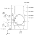
- FIG. 11 is a plan view schematically showing the configuration of an interface reforming device 50a and an internal reforming device 60a according to another embodiment provided with imaging mechanisms 130 and 230.
- FIG. 11 in the following description, in the configurations of the interfacial reforming device 50a and the internal reforming device 60a, elements having substantially the same functional configuration as the interfacial reforming device 50 and the internal reforming device 60 shown in FIG. , are denoted by the same reference numerals, and detailed description thereof will be omitted. Further, as shown in FIG. 11, since the structure of the interfacial reforming device 50a and the internal reforming device 60a are the same, the structure of the interfacial reforming device 50a will be described as a representative example in the following description.
- the interface reforming device 50 a includes a chuck 100 that holds the superimposed wafer T on its upper surface, a laser irradiation unit 110 arranged above the chuck 100 , and a deviation detection unit 120 arranged on the side of the chuck 100 .
- the interface modification device 50a includes an imaging mechanism 130 for imaging the outer edge of the superposed wafer T held by the chuck 100.
- the imaging mechanism 130 is arranged so as to be able to capture an image of the position detected by the displacement amount detection unit 120 at the outer edge of the superposed wafer T from above. That is, the imaging mechanism 130 is arranged above the chuck 100 at the same position in the Y-axis direction as the length measurement sensor 121 of the displacement amount detection unit 120 and on the positive side of the X-axis.
- the imaging mechanism 130 may be configured to be vertically movable by a lifting mechanism (not shown). Note that it is desirable that the positional relationship between the imaging mechanism 130 and the lens 113 of the laser irradiation unit 110 is stored in advance in the control device 90 .
- the imaging mechanism 130 has one or more cameras selected from, for example, a macro camera, a micro camera, etc., and images the outer edge of the superposed wafer T held by the chuck 100 .
- the imaging mechanism 130 includes, for example, a coaxial lens, irradiates light having transparency to at least the first wafer W and the second wafer S, such as infrared light (IR), and receives reflected light from the object. do.
- IR infrared light
- the imaging mechanism 130 moves the superimposed wafer T (in the example of the above embodiment, the second wafer S arranged on the upper side on the chuck 100) in the circumferential direction 360. Take an image of the outer edge at 100 degrees.
- the captured image is output from the imaging mechanism 130 to the control device 90 .
- the control device 90 calculates the amount of eccentricity between the center of rotation of the chuck 100 and the center of the second wafer S from the image of the imaging mechanism 130, and corrects the Y-axis component of the amount of eccentricity based on the calculated amount of eccentricity.
- the chuck 100 is moved in the Y-axis direction.
- control device 90 sets the irradiation area of the interface laser light L1 for forming the bonding force reduction area Ae from the image of the imaging mechanism 130 .
- the irradiation area of the interface laser beam L1 is determined as an annular area having a desired radial width with reference to the outer edge of the second wafer S detected from the image captured by the imaging mechanism 130, for example. Then, in the interface modification apparatus 50, after detecting the amount of displacement between the first wafer W and the second wafer S using the displacement amount detection unit 120, the laser irradiation unit 110 Then, the interface laser beam L1 is irradiated to form the bonding strength decreased region Ae.
- the interface laser light from the laser irradiation unit 110 can be appropriately set within a predetermined irradiation area.
- the imaging mechanisms 130, 230 for detecting the position of the second wafer S) and the shift amount detection units 120, 220 may be arranged independently.
- the bonding strength decrease area Ae and the peripheral modified layer M1 can be formed more appropriately, and the bonding strength can be improved. It is possible to improve the throughput related to the formation of the lowered area Ae and the modified peripheral layer M1.
- the interface laser beam L1 is irradiated from the second wafer S side when forming the bonding force decreased region Ae in the interface modification device 50.
- the interface laser beam L1 may be irradiated from the first wafer W side.
- the bonding force reduction region Ae is formed at the interface between the first wafer W and the bonding film Fw.
- FIG. 12B by irradiating the internal laser beam L2 from the side of the first wafer W, the modified peripheral layer M1 and the divided modified layer M2 are formed inside the first wafer W.
- the peripheral portion We is removed with the modified peripheral layer M1 and the bonding strength reduction region Ae as base points.
- the superposed wafer T from which the peripheral portion We of the first wafer W has been removed is irradiated with a cleaning laser L3 (for example, a femtosecond laser) to form a second wafer S, as shown in FIG.
- a cleaning laser L3 for example, a femtosecond laser
- the surface films (bonding films Fw and Fs and device layers Dw and Ds) remaining on the surface Sa of may be removed.
- the surface film may be removed by, for example, blasting or etching.
- the formation of the bonding force reduction region Ae for the superposed wafer T (step St3) and the formation of the peripheral modified layer M1 and the divided modified layer M2 (step St5) are performed in this order.
- the formation order of these is not particularly limited. That is, after forming the peripheral modified layer M1 and the split modified layer M2 inside the first wafer W in the internal reforming device 60, the first wafer W and the second wafer S are formed in the interface reforming device 50. You may make it form the joining force reduction area
- step St1 the detection of the amount of horizontal misalignment between the first wafer W and the second wafer S (the amount of eccentricity between the first wafer W and the second wafer S) (step St1) is performed by the interface modification device 50. This may be performed by the deviation amount detection section 220 of the internal reforming device 60 instead of the deviation amount detection section 120 .
- the bonding strength decrease region Ae is formed (step St3) for decreasing the bonding strength between the first wafer W and the second wafer S. Forming can be omitted as appropriate.
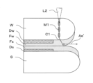
- the modified peripheral layer M1 which is the starting point for removing the peripheral edge We, is formed so as to correspond to the chamfered portion at the outer edge of the first wafer W, as shown in FIG.
- the non-bonded area Ae' which is substantially not bonded by the chamfered portion formed on the peripheral edges of the two wafers, is defined as the bonding strength decreased area.
- the first wafer W may be edge-trimmed by forming the modified peripheral edge layer M1 so as to correspond to the radially inner end of the chamfered portion.
- the chamfered portion (non-bonded area Ae′) of the first wafer W and the second wafer S, which is regarded as the bonding strength decrease area Ae, is determined by the length measurement sensor 121 of the displacement amount detection unit 120 shown in FIGS. It can be detected based on the measurement result (in the example shown in FIG. 5, the measurement result of the central measurement light among the three measurement lights emitted from the length measurement sensor 121).
- the irradiation position of the inner laser beam L2, that is, the formation position of the peripheral modified layer M1 is determined based on the position of the radially inner end of the unbonded region Ae′ detected from the measurement result of the length measurement sensor 121. may be determined.
- the peripheral portion We of the first wafer W is separated from the central portion Wc of the first wafer W with the modified peripheral layer M1 as a base point. Further, since the first wafer W and the second wafer S are not substantially bonded due to the formation of the chamfered portion radially outside the formation position of the peripheral edge modified layer M1, the peripheral edge portion We is appropriately 2 can be removed from the wafer S. Further, according to this example, since it is not necessary to form the bonding strength decreased region Ae in the interface reforming device 50 when edge trimming the first wafer W, the throughput related to edge trimming can be greatly improved.
- the modified peripheral layer M1 when the modified peripheral layer M1 is formed by irradiating the internal laser beam L2, inside the first wafer W, the modified peripheral layer M1 to the first layer is formed.
- the crack C1 extends in the thickness direction of the wafer W.
- the peripheral edge portion We when edge trimming is performed by the peripheral edge removing device 70, the peripheral edge portion We is separated from the central portion Wc with the modified peripheral edge layer M1 and the crack C1 as base points. Therefore, the irradiation position of the interior laser beam L2, that is, the formation position of the peripheral modified layer M1 may be controlled slightly radially inward from the radially inner end portion of the unbonded region Ae' as shown in FIG. .
- the peripheral portion We can be appropriately removed from the overlapped wafer T by extending the crack C1 obliquely from the peripheral edge modified layer M1 toward the radially inner end portion of the unbonded region Ae'.
- such a method of controlling the extension direction of the crack C1 from the modified peripheral layer M1 can be applied even when forming the bonding force decreased region Ae as shown in FIGS. 10 and 12. . That is, in the examples shown in FIGS. 10 and 12, the formation position of the peripheral modified layer M1 is controlled so as to substantially coincide with the inner end portion of the bonding force decrease region Ae in the radial direction, but the method shown in FIG. , the modified peripheral layer M1 may be formed slightly radially inward of the inner end portion of the bonding strength decreased region Ae to extend the crack C1 obliquely.
- the displacement amount detectors 120 and 220 of the interfacial reforming device 50 or the internal reforming device 60 are used to detect the horizontal displacement amount (eccentricity amount) between the first wafer W and the second wafer S. ) is obtained, but the location for obtaining this amount of deviation (amount of eccentricity) is not limited to this.
- the wafer processing system 1 is provided with a deviation detection device (not shown) independently of the interfacial reforming device 50 and the internal reforming device 60. The deviation amount (eccentricity amount) of the wafer S may be acquired.
- the amount of displacement between the first wafer W and the second wafer S (The eccentricity amount) may be obtained, and data of the displacement amount (eccentricity amount) may be output to the control device 90 from these external devices when the superposed wafer T is carried into the wafer processing system 1 .
- the interface modification device for forming the bonding strength decrease area Ae, the peripheral modified layer M1 and the divided modified layer M2 are used.
- An imaging mechanism for detecting the outer edge of the superposed wafer T, which serves as a reference for determining the irradiation positions of the interface laser beam L1 and the internal laser beam L2 is provided in the internal reforming apparatus for forming 130, 230) are required.
- the edge trimming method according to another embodiment the irradiation positions of the interface laser beam L1 and the internal laser beam L2 are determined based on the outer edge of the first wafer W instead of the outer edge of the second wafer S. to align.
- the detailed description of the processing substantially similar to the above-described embodiment based on the outer edge of the second wafer S will be omitted.
- a cassette C containing a plurality of superposed wafers T is mounted on the cassette mounting table 10 of the loading/unloading station 2 .
- the superposed wafer T in the cassette C is taken out by the wafer transfer device 20 and transferred to the interface modification device 50 via the transition device 30 and the wafer transfer device 40 .
- the superposed wafer T is directly transferred from the cassette C to the interface modification device 50. be done.
- the chuck 100 of the interface modification device 50 sucks the entire rear surface Wb of the first wafer W with the second wafer S on the upper side and the first wafer W on the lower side. Hold.
- the shift amount detection unit 120 is used to detect the horizontal shift amount (second The amount of eccentricity between the first wafer W and the second wafer S) is detected (step St1 in FIG. 8).
- the method for detecting the amount of horizontal deviation between the first wafer W and the second wafer S is the same as in the above embodiment.
- a measurement result obtained by the length measurement sensor 121 is output to the calculation section 122 .
- the calculator 122 calculates the outer edge positions of the first wafer W and the second wafer S on the chuck 100 based on the measurement result in step St1. Further, the calculator 122 calculates the amount of horizontal misalignment between the first wafer W and the second wafer S and the eccentricity of the first wafer W and the second wafer S based on the obtained difference value between the distance Lw and the distance Ls. The amount is calculated (step St2 in FIG. 8). The calculated eccentricity amount is output to the control device 90 .
- the controller 90 calculates the amount of eccentricity between the chuck 100 and the second wafer S, that is, the amount of deviation between the rotation center of the chuck 100 and the center of the second wafer S.
- a predetermined irradiation area is irradiated with the interface laser light L1 from the laser irradiation unit 110 in a pulsed manner, and as shown in FIGS.
- a reduced bonding strength region Ae is formed at the interface of the wafer S (in the illustrated example, the interface between the second wafer S and the bonding film Fs) (step St3 in FIG. 8).
- the interface laser light L1 is irradiated toward the overlapped wafer T from the second wafer S side.
- the irradiation area of the interface laser beam L1 is determined as an annular area having a desired radial width with reference to the outer edge of the first wafer W as shown in FIG. 15(a). .
- the radial width of the irradiation region of the interface laser beam L1 is set to a width that can appropriately remove the peripheral edge portion We of the first wafer W to be removed.
- the bonding strength decrease area Ae is formed at a desired position with the outer edge of the first wafer W as a reference.
- the position of the outer edge of the first wafer W which serves as a reference for the irradiation area of the interface laser beam L1 is based on the measurement result (distance Lw) of the length measurement sensor 121 of the deviation amount detection unit 120 described above. , the irradiation area of the interface laser beam L1 can be appropriately detected. Further, in this embodiment, as described above, the positional relationship between the length measuring sensor 121 and the lens 113 of the laser irradiation unit 110 is stored in advance. Based on this, the irradiation position of the interface laser beam L1 can be appropriately set within the irradiation area.
- the outer edges of the first wafer W and the second wafer S are detected by using the deviation detection unit 120 including the length measurement sensor 121 provided on the side of the chuck 100 as described above. Each is detected independently. For this reason, compared with the conventional case where the deviation amount of the second wafer S is observed from above the superimposed wafer T, for example, the irradiation of the interface laser light L1 with the outer end portion of the second wafer S as a reference is Positional alignment can be performed properly.
- the irradiation of the interface laser beam L1 to the superposed wafer T may be performed from the second wafer S side as described above, or may be performed from the first wafer W side.
- the superposed wafer T in which the bonding strength decreased area Ae is formed at the interface between the first wafer W and the second wafer S is transferred to the reversing device 31 by the wafer transfer device 40 .
- the reversing device 31 reverses the front and rear surfaces of the superposed wafer T so that the first wafer W faces upward.
- the superposed wafer T whose front and back surfaces are reversed is then transferred to the internal reforming device 60 by the wafer transfer device 40 .
- the chuck 200 of the internal reforming device 60 sucks and holds the entire back surface Sb of the second wafer S with the first wafer W on the upper side and the second wafer S on the lower side. .
- the position of the superposed wafer T held by the chuck 200 is detected using the length measurement sensor 221 of the deviation amount detection section 220 (step St4 in FIG. 8).
- a measurement result by the length measurement sensor 221 is output to the calculation section 222 .
- the eccentricity calculated by the calculator 222 is output to the control device 90 . Further, the controller 90 acquires the amount of eccentricity between the chuck 200 and the second wafer S, that is, the amount of deviation between the rotation center of the chuck 200 and the center of the second wafer S.
- the internal laser beam L2 is irradiated from the laser irradiation unit 210 to a predetermined irradiation position of the internal laser beam L2, and as shown in FIGS. 3 and 15B, the first wafer W A peripheral modified layer M1 and a divided modified layer M2 are sequentially formed inside (step St5 in FIG. 8).
- the internal laser beam L2 is irradiated toward the overlapped wafer T from the first wafer W side.
- the irradiation position of the internal laser beam L2, that is, the formation position of the peripheral edge modified layer M1 is, for example, the outer edge of the first wafer W as a reference, and is radially inward of the bonding strength decreased region Ae formed in step St3. It is determined slightly radially inward from the end.
- the peripheral modified layer M1 is formed at a desired position with the outer edge of the first wafer W as a reference.
- the position of the outer edge of the first wafer W which serves as a reference for the formation position of the modified peripheral layer M1 is obtained in advance based on the measurement result (distance Lw) by the above-described length measurement sensor 221, and Since the positional relationship between the length measurement sensor 221 and the lens 213 of the laser irradiation unit 210 is stored in advance, the irradiation position of the internal laser beam L2 can be properly aligned to a desired position.
- the superposed wafer T in which the modified edge layer M1 and the divided modified layer M2 are formed inside the first wafer W is then transferred to the edge removing apparatus 70 by the wafer transfer apparatus 40 .
- the peripheral edge removal device 70 removes the peripheral edge portion We of the first wafer W, that is, performs edge trimming (step St6 in FIG. 8).
- the removal of the peripheral portion We may be performed by inserting the blade B into the interface between the first wafer W and the second wafer S, and the insertion position of the blade B is determined based on the measurement results in step St1. may be
- the superposed wafer T from which the peripheral portion We of the first wafer W has been removed is then transferred to the cleaning device 80 by the wafer transfer device 40 .
- the cleaning device 80 cleans the first wafer W and/or the second wafer S from which the peripheral portion We has been removed (step St7 in FIG. 8). Further, when the surface film remains on the surface Sa of the second wafer S after the removal of the peripheral portion We, as shown in FIG. 15D, even if the surface film is further removed, good.
- the superposed wafer T that has undergone all the processes is transferred to the transition device 30 by the wafer transfer device 40 and transferred to the cassette C on the cassette mounting table 10 by the wafer transfer device 20 .
- a series of wafer processing in the wafer processing system 1 is completed.
- edge trimming For the superimposed wafer T on which the edge trimming of the first wafer W has been performed, it is determined whether the edge trimming has been properly performed, that is, whether the peripheral edge portion We has been removed from the first wafer W with the desired trim width.
- An inspection performance inspection may be performed to determine whether or not it is acceptable.
- edge trim processing according to another embodiment as shown in FIG. It can be uniformly controlled over the entire circumference of W.
- the length measuring sensor is used to independently detect the outer edges of the first wafer W and the second wafer S. , the outer edge of the first wafer W, or the outer edge of the second wafer S, and the irradiation positions of the interface laser beam L1 and the internal laser beam L2 can decide.
- the selection of the reference position of the laser beam irradiation position can be changed by the controller 90 for each lot accommodated in the cassette C or for each wafer processed by the wafer processing system 1, for example. is also possible.
Landscapes
- Physics & Mathematics (AREA)
- Optics & Photonics (AREA)
- Engineering & Computer Science (AREA)
- Plasma & Fusion (AREA)
- Mechanical Engineering (AREA)
- Chemical & Material Sciences (AREA)
- Chemical Kinetics & Catalysis (AREA)
- General Chemical & Material Sciences (AREA)
- Oil, Petroleum & Natural Gas (AREA)
- Container, Conveyance, Adherence, Positioning, Of Wafer (AREA)
- Mechanical Treatment Of Semiconductor (AREA)
Priority Applications (4)
| Application Number | Priority Date | Filing Date | Title |
|---|---|---|---|
| KR1020247030382A KR20240148891A (ko) | 2022-02-18 | 2023-01-23 | 처리 방법 및 처리 시스템 |
| CN202380020778.6A CN118661245A (zh) | 2022-02-18 | 2023-01-23 | 处理方法和处理系统 |
| JP2024501044A JP7851390B2 (ja) | 2022-02-18 | 2023-01-23 | 処理方法及び処理システム |
| US18/839,180 US20250153278A1 (en) | 2022-02-18 | 2023-01-23 | Processing method and processing system |
Applications Claiming Priority (2)
| Application Number | Priority Date | Filing Date | Title |
|---|---|---|---|
| JP2022024175 | 2022-02-18 | ||
| JP2022-024175 | 2022-02-18 |
Publications (1)
| Publication Number | Publication Date |
|---|---|
| WO2023157566A1 true WO2023157566A1 (ja) | 2023-08-24 |
Family
ID=87578373
Family Applications (1)
| Application Number | Title | Priority Date | Filing Date |
|---|---|---|---|
| PCT/JP2023/001867 Ceased WO2023157566A1 (ja) | 2022-02-18 | 2023-01-23 | 処理方法及び処理システム |
Country Status (6)
| Country | Link |
|---|---|
| US (1) | US20250153278A1 (https=) |
| JP (1) | JP7851390B2 (https=) |
| KR (1) | KR20240148891A (https=) |
| CN (1) | CN118661245A (https=) |
| TW (1) | TW202338958A (https=) |
| WO (1) | WO2023157566A1 (https=) |
Cited By (2)
| Publication number | Priority date | Publication date | Assignee | Title |
|---|---|---|---|---|
| WO2025216062A1 (ja) * | 2024-04-09 | 2025-10-16 | 東京エレクトロン株式会社 | 基板処理システム、基板処理方法及びコンピュータ記憶媒体 |
| WO2026034270A1 (ja) * | 2024-08-09 | 2026-02-12 | 東京エレクトロン株式会社 | 基板処理システム及び基板処理方法 |
Families Citing this family (1)
| Publication number | Priority date | Publication date | Assignee | Title |
|---|---|---|---|---|
| JP2024127237A (ja) * | 2023-03-09 | 2024-09-20 | 株式会社ディスコ | ウエーハの加工方法 |
Citations (5)
| Publication number | Priority date | Publication date | Assignee | Title |
|---|---|---|---|---|
| JP2019174262A (ja) * | 2018-03-28 | 2019-10-10 | 株式会社東京精密 | 貼り合せ基板の測定方法および加工方法並びにそれらに用いる装置 |
| WO2020084909A1 (ja) * | 2018-10-23 | 2020-04-30 | 東京エレクトロン株式会社 | 基板処理装置及び基板処理方法 |
| JP2020093360A (ja) * | 2018-12-14 | 2020-06-18 | 株式会社東京精密 | 貼り合わせウェーハのエッジトリミング加工方法 |
| JP2021174806A (ja) * | 2020-04-20 | 2021-11-01 | 東京エレクトロン株式会社 | 基板処理装置及び基板処理方法 |
| JP2022002312A (ja) * | 2018-04-27 | 2022-01-06 | 東京エレクトロン株式会社 | 基板処理システム及び基板処理方法 |
Family Cites Families (1)
| Publication number | Priority date | Publication date | Assignee | Title |
|---|---|---|---|---|
| CN118263105A (zh) | 2018-03-14 | 2024-06-28 | 东京毅力科创株式会社 | 基板处理系统、基板处理方法以及计算机存储介质 |
-
2023
- 2023-01-23 JP JP2024501044A patent/JP7851390B2/ja active Active
- 2023-01-23 KR KR1020247030382A patent/KR20240148891A/ko active Pending
- 2023-01-23 US US18/839,180 patent/US20250153278A1/en active Pending
- 2023-01-23 CN CN202380020778.6A patent/CN118661245A/zh active Pending
- 2023-01-23 WO PCT/JP2023/001867 patent/WO2023157566A1/ja not_active Ceased
- 2023-02-09 TW TW112104491A patent/TW202338958A/zh unknown
Patent Citations (5)
| Publication number | Priority date | Publication date | Assignee | Title |
|---|---|---|---|---|
| JP2019174262A (ja) * | 2018-03-28 | 2019-10-10 | 株式会社東京精密 | 貼り合せ基板の測定方法および加工方法並びにそれらに用いる装置 |
| JP2022002312A (ja) * | 2018-04-27 | 2022-01-06 | 東京エレクトロン株式会社 | 基板処理システム及び基板処理方法 |
| WO2020084909A1 (ja) * | 2018-10-23 | 2020-04-30 | 東京エレクトロン株式会社 | 基板処理装置及び基板処理方法 |
| JP2020093360A (ja) * | 2018-12-14 | 2020-06-18 | 株式会社東京精密 | 貼り合わせウェーハのエッジトリミング加工方法 |
| JP2021174806A (ja) * | 2020-04-20 | 2021-11-01 | 東京エレクトロン株式会社 | 基板処理装置及び基板処理方法 |
Cited By (2)
| Publication number | Priority date | Publication date | Assignee | Title |
|---|---|---|---|---|
| WO2025216062A1 (ja) * | 2024-04-09 | 2025-10-16 | 東京エレクトロン株式会社 | 基板処理システム、基板処理方法及びコンピュータ記憶媒体 |
| WO2026034270A1 (ja) * | 2024-08-09 | 2026-02-12 | 東京エレクトロン株式会社 | 基板処理システム及び基板処理方法 |
Also Published As
| Publication number | Publication date |
|---|---|
| JPWO2023157566A1 (https=) | 2023-08-24 |
| TW202338958A (zh) | 2023-10-01 |
| JP7851390B2 (ja) | 2026-04-24 |
| KR20240148891A (ko) | 2024-10-11 |
| US20250153278A1 (en) | 2025-05-15 |
| CN118661245A (zh) | 2024-09-17 |
Similar Documents
| Publication | Publication Date | Title |
|---|---|---|
| WO2023157566A1 (ja) | 処理方法及び処理システム | |
| JP7134330B2 (ja) | 基板処理装置及び基板処理方法 | |
| JP7157816B2 (ja) | 基板処理装置及び基板処理方法 | |
| KR101431838B1 (ko) | 반도체 웨이퍼로의 점착 테이프 부착 방법 및 보호테이프의 박리 방법 | |
| CN113165109B (zh) | 基板处理装置和基板处理方法 | |
| JP7611350B2 (ja) | 基板処理装置及び基板処理方法 | |
| JP7780534B2 (ja) | 処理方法及び処理システム | |
| JP7688216B2 (ja) | 基板処理方法及び基板処理装置 | |
| JP7129549B2 (ja) | 処理装置及び処理方法 | |
| KR101467121B1 (ko) | 웨이퍼 표면 검사 장치 | |
| JP2026063154A (ja) | 基板処理システム及び基板処理方法 | |
| JP7297074B2 (ja) | 検査装置の自己診断方法および検査装置 | |
| JP2023003476A (ja) | 処理方法及び処理システム | |
| JP2024087506A (ja) | 基板処理方法及びウェハ処理システム | |
| WO2026004650A1 (ja) | 基板処理システム、基板処理方法、プログラム及び記憶媒体 |
Legal Events
| Date | Code | Title | Description |
|---|---|---|---|
| 121 | Ep: the epo has been informed by wipo that ep was designated in this application |
Ref document number: 23756094 Country of ref document: EP Kind code of ref document: A1 |
|
| WWE | Wipo information: entry into national phase |
Ref document number: 202380020778.6 Country of ref document: CN |
|
| ENP | Entry into the national phase |
Ref document number: 2024501044 Country of ref document: JP Kind code of ref document: A |
|
| WWE | Wipo information: entry into national phase |
Ref document number: 18839180 Country of ref document: US |
|
| ENP | Entry into the national phase |
Ref document number: 20247030382 Country of ref document: KR Kind code of ref document: A |
|
| WWE | Wipo information: entry into national phase |
Ref document number: 1020247030382 Country of ref document: KR |
|
| NENP | Non-entry into the national phase |
Ref country code: DE |
|
| 122 | Ep: pct application non-entry in european phase |
Ref document number: 23756094 Country of ref document: EP Kind code of ref document: A1 |
|
| WWP | Wipo information: published in national office |
Ref document number: 18839180 Country of ref document: US |