WO2023157531A1 - 光電変換素子および撮像装置 - Google Patents
光電変換素子および撮像装置 Download PDFInfo
- Publication number
- WO2023157531A1 WO2023157531A1 PCT/JP2023/001179 JP2023001179W WO2023157531A1 WO 2023157531 A1 WO2023157531 A1 WO 2023157531A1 JP 2023001179 W JP2023001179 W JP 2023001179W WO 2023157531 A1 WO2023157531 A1 WO 2023157531A1
- Authority
- WO
- WIPO (PCT)
- Prior art keywords
- quantum dot
- electrode
- photoelectric conversion
- layer
- energy
- Prior art date
- Legal status (The legal status is an assumption and is not a legal conclusion. Google has not performed a legal analysis and makes no representation as to the accuracy of the status listed.)
- Ceased
Links
Images




Classifications
-
- C—CHEMISTRY; METALLURGY
- C09—DYES; PAINTS; POLISHES; NATURAL RESINS; ADHESIVES; COMPOSITIONS NOT OTHERWISE PROVIDED FOR; APPLICATIONS OF MATERIALS NOT OTHERWISE PROVIDED FOR
- C09K—MATERIALS FOR MISCELLANEOUS APPLICATIONS, NOT PROVIDED FOR ELSEWHERE
- C09K11/00—Luminescent materials, e.g. electroluminescent or chemiluminescent
- C09K11/02—Use of particular materials as binders, particle coatings or suspension media therefor
- C09K11/025—Use of particular materials as binders, particle coatings or suspension media therefor non-luminescent particle coatings or suspension media
-
- H—ELECTRICITY
- H10—SEMICONDUCTOR DEVICES; ELECTRIC SOLID-STATE DEVICES NOT OTHERWISE PROVIDED FOR
- H10F—INORGANIC SEMICONDUCTOR DEVICES SENSITIVE TO INFRARED RADIATION, LIGHT, ELECTROMAGNETIC RADIATION OF SHORTER WAVELENGTH OR CORPUSCULAR RADIATION
- H10F30/00—Individual radiation-sensitive semiconductor devices in which radiation controls the flow of current through the devices, e.g. photodetectors
- H10F30/20—Individual radiation-sensitive semiconductor devices in which radiation controls the flow of current through the devices, e.g. photodetectors the devices having potential barriers, e.g. phototransistors
-
- H—ELECTRICITY
- H10—SEMICONDUCTOR DEVICES; ELECTRIC SOLID-STATE DEVICES NOT OTHERWISE PROVIDED FOR
- H10F—INORGANIC SEMICONDUCTOR DEVICES SENSITIVE TO INFRARED RADIATION, LIGHT, ELECTROMAGNETIC RADIATION OF SHORTER WAVELENGTH OR CORPUSCULAR RADIATION
- H10F39/00—Integrated devices, or assemblies of multiple devices, comprising at least one element covered by group H10F30/00, e.g. radiation detectors comprising photodiode arrays
- H10F39/10—Integrated devices
- H10F39/12—Image sensors
-
- H—ELECTRICITY
- H10—SEMICONDUCTOR DEVICES; ELECTRIC SOLID-STATE DEVICES NOT OTHERWISE PROVIDED FOR
- H10K—ORGANIC ELECTRIC SOLID-STATE DEVICES
- H10K30/00—Organic devices sensitive to infrared radiation, light, electromagnetic radiation of shorter wavelength or corpuscular radiation
- H10K30/30—Organic devices sensitive to infrared radiation, light, electromagnetic radiation of shorter wavelength or corpuscular radiation comprising bulk heterojunctions, e.g. interpenetrating networks of donor and acceptor material domains
- H10K30/35—Organic devices sensitive to infrared radiation, light, electromagnetic radiation of shorter wavelength or corpuscular radiation comprising bulk heterojunctions, e.g. interpenetrating networks of donor and acceptor material domains comprising inorganic nanostructures, e.g. CdSe nanoparticles
-
- H—ELECTRICITY
- H10—SEMICONDUCTOR DEVICES; ELECTRIC SOLID-STATE DEVICES NOT OTHERWISE PROVIDED FOR
- H10K—ORGANIC ELECTRIC SOLID-STATE DEVICES
- H10K39/00—Integrated devices, or assemblies of multiple devices, comprising at least one organic radiation-sensitive element covered by group H10K30/00
- H10K39/30—Devices controlled by radiation
- H10K39/32—Organic image sensors
-
- B—PERFORMING OPERATIONS; TRANSPORTING
- B82—NANOTECHNOLOGY
- B82Y—SPECIFIC USES OR APPLICATIONS OF NANOSTRUCTURES; MEASUREMENT OR ANALYSIS OF NANOSTRUCTURES; MANUFACTURE OR TREATMENT OF NANOSTRUCTURES
- B82Y20/00—Nanooptics, e.g. quantum optics or photonic crystals
-
- Y—GENERAL TAGGING OF NEW TECHNOLOGICAL DEVELOPMENTS; GENERAL TAGGING OF CROSS-SECTIONAL TECHNOLOGIES SPANNING OVER SEVERAL SECTIONS OF THE IPC; TECHNICAL SUBJECTS COVERED BY FORMER USPC CROSS-REFERENCE ART COLLECTIONS [XRACs] AND DIGESTS
- Y02—TECHNOLOGIES OR APPLICATIONS FOR MITIGATION OR ADAPTATION AGAINST CLIMATE CHANGE
- Y02E—REDUCTION OF GREENHOUSE GAS [GHG] EMISSIONS, RELATED TO ENERGY GENERATION, TRANSMISSION OR DISTRIBUTION
- Y02E10/00—Energy generation through renewable energy sources
- Y02E10/50—Photovoltaic [PV] energy
- Y02E10/549—Organic PV cells
Definitions
- the present disclosure relates to photoelectric conversion elements and imaging devices.
- a semiconductor quantum dot refers to a nanocrystal, which is a semiconductor microcrystal with a size of several nanometers.
- the energy state is discretized by the confinement of electrons, holes, and excitons in the nanocrystals, and the energy shift depending on the particle size appears, which is called the quantum size effect. Since the bandgap energy of semiconductor quantum dots, which are nanocrystals, becomes larger than that of bulk crystals as the particle size becomes smaller, the absorption edge wavelength shifts to the short wavelength side.
- quantum dots may be simply referred to as “quantum dots”.
- quantum dots When quantum dots are used as a photoelectric conversion material, it is desirable that the sensitivity wavelength region is widened according to the application.
- Non-Patent Document 1 discloses a solar cell capable of broadening the sensitivity wavelength region by stacking a plurality of quantum dots with different particle sizes to form a photoelectric conversion layer.
- non-patent document 1 discloses the widening of the sensitivity wavelength when quantum dots are used as a photoelectric conversion material, it is important when quantum dots are used in the photoelectric conversion layer of an imaging device or the like.
- suitable laminate structures for sensitivity, dark current and response speed For example, in imagers, sensitivity and dark current are directly linked to the signal/noise (S/N) ratio.
- S/N signal/noise
- the response speed required for photoelectric conversion elements used in imaging devices is faster than the response speed of solar cells.
- An object of the present disclosure is to provide a photoelectric conversion element and an imaging device that can achieve both expansion of the sensitivity wavelength range and improvement of sensitivity when quantum dots are used in the photoelectric conversion layer.
- a photoelectric conversion element includes a photoelectric conversion layer, a first electrode that collects holes generated in the photoelectric conversion layer as signal charges, and the first electrode with the photoelectric conversion layer interposed therebetween. and a second electrode that faces and collects electrons generated in the photoelectric conversion layer.
- the photoelectric conversion layer includes three or more quantum dot layers laminated to each other, and each of the three or more quantum dot layers includes a quantum dot and a surface-modifying ligand that modifies the surface of the quantum dot. .
- the bandgap energy of the quantum dot layer near the first electrode is the quantum dot near the second electrode smaller than the bandgap energy of the layer.
- the energy relationship at the interface between each of the three or more quantum dot layers and the quantum dot layer adjacent to each of the three or more quantum dot layers is expressed by the following formulas (1) and (2). satisfy at least one of
- E i CBM is the energy at the bottom of the conduction band of the i-th quantum dot layer counting from the first electrode among the three or more quantum dot layers
- E i+1 CBM is the three or more quantum dot layers. It is the energy at the bottom of the conduction band of the i+1-th quantum dot layer counting from the first electrode among the dot layers
- E i VBM is the i-th quantum dot layer counting from the first electrode among the three or more quantum dot layers.
- E i+1 VBM is the energy at the top of the valence band of the i+1-th quantum dot layer counted from the first electrode among the three or more quantum dot layers.
- a photoelectric conversion element includes a photoelectric conversion layer, a first electrode that collects electrons generated in the photoelectric conversion layer as signal charges, and faces the first electrode with the photoelectric conversion layer interposed therebetween. and a second electrode that collects holes generated in the photoelectric conversion layer.
- the photoelectric conversion layer includes three or more quantum dot layers stacked together, and each of the three or more quantum dot layers includes quantum dots.
- the bandgap energy of the quantum dot layer near the first electrode is the quantum dot near the second electrode smaller than the bandgap energy of the layer.
- the energy relationship at the interface between each of the three or more quantum dot layers and the quantum dot layer adjacent to each of the three or more quantum dot layers is expressed by the following formulas (4) and (5). satisfy at least one of
- E i CBM is the energy at the bottom of the conduction band of the i-th quantum dot layer counting from the first electrode among the three or more quantum dot layers
- E i+1 CBM is the three or more quantum dot layers. It is the energy at the bottom of the conduction band of the i+1-th quantum dot layer counting from the first electrode among the dot layers
- E i VBM is the i-th quantum dot layer counting from the first electrode among the three or more quantum dot layers.
- E i+1 VBM is the energy at the top of the valence band of the i+1-th quantum dot layer counted from the first electrode among the three or more quantum dot layers.
- an imaging device includes a plurality of pixels each including the photoelectric conversion element, a signal readout circuit connected to the first electrode, and a voltage supply that supplies voltage to the second electrode. a circuit;
- FIG. 1 is a cross-sectional view schematically showing the configuration of a photoelectric conversion element according to Embodiment 1.
- FIG. 2A is a cross-sectional view schematically showing the configuration of another photoelectric conversion element according to Embodiment 1.
- FIG. 2B is a diagram showing an example of an energy diagram of the photoelectric conversion element shown in FIG. 2A.
- 3 is a diagram showing an example of an energy diagram of a photoelectric conversion layer according to Embodiment 1.
- FIG. FIG. 4A is a diagram for explaining an energy barrier at the interface between two adjacent quantum dot layers.
- FIG. 4B is another diagram for explaining the energy barrier at the interface of two adjacent quantum dot layers.
- FIG. 5 is a diagram showing an example of an energy diagram of a photoelectric conversion layer according to Embodiment 2.
- FIG. FIG. 6 is a diagram showing an example of an energy diagram of a photoelectric conversion layer according to Embodiment 3.
- FIG. 7A is a diagram showing an example of an energy diagram of a photoelectric conversion layer according to Embodiment 4.
- FIG. 7B is a diagram schematically showing an example of an absorption spectrum of each quantum dot layer according to Embodiment 4.
- FIG. 7C is a diagram for explaining absorption of light including the absorption peak wavelength of each quantum dot layer in the photoelectric conversion layer according to Embodiment 4.
- FIG. 7D is a diagram for explaining absorption of light including the absorption peak wavelength of each quantum dot layer in another photoelectric conversion layer.
- FIG. 8 is a diagram showing an example of an energy diagram of a photoelectric conversion layer according to Embodiment 5.
- FIG. FIG. 9 is a diagram illustrating an example of a circuit configuration of an imaging device according to Embodiment 6.
- FIG. 10 is a cross-sectional view schematically showing a device structure of a pixel in an imaging device according to Embodiment 6.
- a photoelectric conversion element includes a photoelectric conversion layer, a first electrode that collects holes generated in the photoelectric conversion layer as signal charges, and the first electrode with the photoelectric conversion layer interposed therebetween. and a second electrode that faces and collects electrons generated in the photoelectric conversion layer.
- the photoelectric conversion layer includes three or more quantum dot layers laminated to each other, and each of the three or more quantum dot layers includes a quantum dot and a surface-modifying ligand that modifies the surface of the quantum dot. .
- the bandgap energy of the quantum dot layer near the first electrode is the quantum dot near the second electrode smaller than the bandgap energy of the layer.
- the energy relationship at the interface between each of the three or more quantum dot layers and the quantum dot layer adjacent to each of the three or more quantum dot layers is expressed by the following formulas (1) and (2). satisfy at least one of
- E i CBM is the energy at the bottom of the conduction band of the i-th quantum dot layer counting from the first electrode among the three or more quantum dot layers
- E i+1 CBM is the three or more quantum dot layers. It is the energy at the bottom of the conduction band of the i+1-th quantum dot layer counting from the first electrode among the dot layers
- E i VBM is the i-th quantum dot layer counting from the first electrode among the three or more quantum dot layers.
- E i+1 VBM is the energy at the top of the valence band of the i+1-th quantum dot layer counted from the first electrode among the three or more quantum dot layers.
- the bandgap energy of the quantum dot layer close to the first electrode is smaller than the bandgap energy of the quantum dot layer close to the second electrode.
- Light having an absorption peak wavelength of the quantum dot layer closer to the first electrode out of the two quantum dot layers is less likely to be absorbed by the quantum dot layer closer to the second electrode.
- photoelectric conversion is likely to occur in the quantum dot layer near the first electrode where the signal charge is collected, and the first electrode is likely to collect the signal charge. Therefore, the sensitivity of the photoelectric conversion element can be improved.
- three or more quantum dot layers include a combination of two adjacent quantum dot layers with different bandgap energies, quantum dot layers with different absorption peak wavelengths are stacked. Therefore, the sensitivity wavelength region of the photoelectric conversion element can be expanded.
- the photoelectric conversion element according to this aspect can achieve both the expansion of the sensitivity wavelength range and the improvement of the sensitivity.
- the energy relationship at the interface may satisfy both the formula (1) and the formula (2).
- the energy relationship at the interface may satisfy the following formula (3).
- a photoelectric conversion element includes a photoelectric conversion layer, a first electrode that collects electrons generated in the photoelectric conversion layer as signal charges, and the first electrode with the photoelectric conversion layer interposed therebetween. and a second electrode facing to collect holes generated in the photoelectric conversion layer.
- the photoelectric conversion layer includes three or more quantum dot layers stacked together, and each of the three or more quantum dot layers includes quantum dots.
- the bandgap energy of the quantum dot layer near the first electrode is the quantum dot near the second electrode smaller than the bandgap energy of the layer.
- the energy relationship at the interface between each of the three or more quantum dot layers and the quantum dot layer adjacent to each of the three or more quantum dot layers is expressed by the following formulas (4) and (5). satisfy at least one of
- E i CBM is the energy at the bottom of the conduction band of the i-th quantum dot layer counting from the first electrode among the three or more quantum dot layers
- E i+1 CBM is the three or more quantum dot layers. It is the energy at the bottom of the conduction band of the i+1-th quantum dot layer counting from the first electrode among the dot layers
- E i VBM is the i-th quantum dot layer counting from the first electrode among the three or more quantum dot layers.
- E i+1 VBM is the energy at the top of the valence band of the i+1-th quantum dot layer counted from the first electrode among the three or more quantum dot layers.
- the bandgap energy of the quantum dot layer near the first electrode is smaller than the bandgap energy of the quantum dot layer near the second electrode, so that the adjacent quantum dot layers Light having an absorption peak wavelength of the quantum dot layer closer to the first electrode out of the two quantum dot layers is less likely to be absorbed by the quantum dot layer closer to the second electrode.
- photoelectric conversion is likely to occur in the quantum dot layer near the first electrode where the signal charge is collected, and the first electrode is likely to collect the signal charge. Therefore, the sensitivity of the photoelectric conversion element can be improved.
- three or more quantum dot layers include a combination of two adjacent quantum dot layers with different bandgap energies, quantum dot layers with different absorption peak wavelengths are stacked. Therefore, the sensitivity wavelength region of the photoelectric conversion element can be expanded.
- the photoelectric conversion element according to this aspect can achieve both the expansion of the sensitivity wavelength range and the improvement of the sensitivity.
- the energy relationship at the interface may satisfy both the formula (4) and the formula (5).
- the energy relationship at the interface may satisfy the following formula (6).
- the potential gradient for the signal charge may be equal to or greater than the potential gradient for the opposite polarity charge of the signal charge.
- the particle diameter of the quantum dots contained in the quantum dot layer close to the second electrode is a quantum close to the first electrode It may be smaller than the particle size of the quantum dots contained in the dot layer.
- the particle diameters of the quantum dots included in each of the three or more quantum dot layers may decrease in order from the first electrode side.
- the bandgap energy of the quantum dot layer close to the first electrode is smaller than the bandgap energy of the quantum dot layer close to the second electrode.
- a dot layer can be easily realized.
- the absorption peak wavelength of the quantum dot layer close to the second electrode is the absorption peak wavelength of the quantum dot layer close to the first electrode. It may be shorter than the wavelength. In other words, the absorption peak wavelengths of the three or more quantum dot layers may decrease in order from the first electrode side.
- the quantum dot layer also has an absorption wavelength region on the short wavelength side of the absorption peak wavelength, but with such a configuration of three or more quantum dot layers, in all combinations of two adjacent quantum dot layers, the first Light having an absorption peak wavelength of the quantum dot layer close to the electrode is less likely to be absorbed by the quantum dot layer close to the second electrode. Therefore, the sensitivity of the photoelectric conversion element can be further improved.
- each of the three or more quantum dot layers further includes a surface-modifying ligand that modifies the surface of the quantum dots, and is contained in at least two of the three or more quantum dot layers.
- the surface-modifying ligands may be different from each other.
- the energy at the top of the valence band of the quantum dot layer can be adjusted according to the type of surface-modifying ligand, so a quantum dot layer having a desired energy band can be easily realized.
- each of the three or more quantum dot layers further includes a surface-modifying ligand that modifies the surface of the quantum dots, and is contained in at least two of the three or more quantum dot layers. Densities of the surface-modifying ligands may differ from each other.
- the energy of the upper end of the valence band of the quantum dot layer can be adjusted by the density of the surface-modifying ligand, so a quantum dot layer having a desired energy band can be easily realized.
- the quantum dots include CdSe, CdS, PbS, PbSe, PbTe, ZnO, ZnS, Cu2ZnSnS4 , Cu2S , CuInSe2 , AgInS2 , AgInTe2 , CdSnAs2, ZnSnAs2 , ZnSnSb2 , At least one selected from the group consisting of Bi 2 S 3 , Ag 2 S, Ag 2 Te, AgBiS 2 , AgAuS, HgTe, CdHgTe, Ge, GeSn, InAs and InSb may be included.
- the sensitivity wavelength of the photoelectric conversion element can be arbitrarily controlled in a wide wavelength range from visible light to infrared light.
- an imaging device includes a plurality of pixels each including the photoelectric conversion element, a signal readout circuit connected to the first electrode, and a voltage supply that supplies voltage to the second electrode. a circuit;
- the imaging device since the imaging device has the photoelectric conversion element, it is possible to expand the sensitivity wavelength range and improve the sensitivity.
- the terms “upper” and “lower” do not refer to the upward direction (vertically upward) and the downward direction (vertically downward) in absolute spatial recognition, but are based on the stacking order in the stacking structure. It is used as a term defined by a relative positional relationship. Note that terms such as “upper” and “lower” are used only to specify the mutual arrangement of members, and are not intended to limit the orientation of the imaging apparatus when it is used. Also, the terms “above” and “below” are used not only when two components are spaced apart from each other and there is another component between the two components, but also when two components are spaced apart from each other. It also applies when two components are in contact with each other and are placed in close contact with each other.
- FIG. 1 is a cross-sectional view schematically showing the configuration of a photoelectric conversion element 10A according to this embodiment.
- the photoelectric conversion element 10A includes a first electrode 2 , a second electrode 3 , and a photoelectric conversion layer 4 positioned between the first electrode 2 and the second electrode 3 .
- the photoelectric conversion layer 4 has n layers of quantum dot layers in order to expand the sensitivity wavelength region, and has a structure in which n layers of quantum dot layers are stacked.
- the photoelectric conversion layer 4 includes the first quantum dot layer 4a, the second quantum dot layer 4b, the third quantum dot layer 4c, the fourth quantum dot layer 4d, and the fifth quantum dot layer 4e. It has a structure in which quantum dot layers of layers are stacked.
- the number of quantum dot layers included in the photoelectric conversion layer 4 is not particularly limited. n may be, for example, 4 or more, or 5 or more. As the number of n increases, the movement of charges in the photoelectric conversion layer 4 is more likely to be hindered, making it more difficult to improve sensitivity. is further enlarged, the sensitivity of the photoelectric conversion element can be effectively improved. Also, n may be 10 or less, or may be 7 or less.
- the five quantum dot layers from the first quantum dot layer 4a to the fifth quantum dot layer 4e have different absorption peak wavelengths.
- the first quantum dot layer 4a, the second quantum dot layer 4b, the third quantum dot layer 4c, the fourth quantum dot layer 4d and the fifth quantum dot layer 4e are arranged in this order from the first electrode 2 side. is laminated with
- the photoelectric conversion element 10A is supported by the substrate 1.
- a first electrode 2, a photoelectric conversion layer 4, and a second electrode 3 are laminated in this order on one main surface of a substrate 1. As shown in FIG.
- FIG. 2A is a cross-sectional view schematically showing the configuration of a photoelectric conversion element 10B as another example according to the present embodiment.
- FIG. 2B is a diagram showing an example of an energy diagram of the photoelectric conversion element 10B shown in FIG. 2A.
- FIG. 2B schematically shows the energy band of each layer as a rectangle.
- FIG. 2B is a diagram showing that the lower, that is, the greater the difference from the vacuum level, the greater the energy.
- the top of the rectangle shown in FIG. 2B is the energy of the conduction band bottom or LUMO (Lowest Unoccupied Molecular Orbital).
- the difference between the vacuum level and the lower end of the conduction band or LUMO energy is the electron affinity
- the difference between the vacuum level and the upper end of the valence band or HOMO energy is the ionization potential.
- the work function is the difference between the Fermi level and the vacuum level.
- the bandgap energy is the difference between the energy at the lower end of the conduction band and the energy at the upper end of the valence band, or the difference between the LUMO energy and the HOMO energy.
- the photoelectric conversion element 10B includes, in addition to the configuration of the photoelectric conversion element 10A, an electron blocking layer 5 located between the first electrode 2 and the photoelectric conversion layer 4, a second electrode 3 and a photoelectric conversion layer 5. and a hole blocking layer 6 positioned between the conversion layer 4 .
- first electrode 2, electron blocking layer 5, photoelectric conversion layer 4, hole blocking layer 6, and second electrode 3 are laminated in this order on one main surface of substrate 1.
- FIG. Although details will be described later, this configuration can reduce dark current when a reverse bias voltage is applied during photoelectric conversion.
- the substrate 1 is a support substrate that supports the photoelectric conversion elements 10A and 10B.
- the material of the substrate 1 is not particularly limited, and various materials can be used. For example, it may be a p-type silicon substrate on which an insulating layer is formed, or a glass or plastic substrate coated with a conductive metal oxide such as ITO (Indium Tin Oxide) or a conductive polymer such as polyacetylene. .
- the substrate 1 may transmit at least part of the light having the wavelength that the photoelectric conversion layer 4 absorbs.
- the substrate 1 is arranged, for example, on the side opposite to the light incident side of the photoelectric conversion elements 10A and 10B.
- the substrate 1 is arranged near the first electrode 2 in the photoelectric conversion element 10A and the photoelectric conversion element 10B, but the second electrode 3 in the photoelectric conversion element 10A and the photoelectric conversion element 10B may be located near the
- the first electrode 2 and the second electrode 3 are, for example, film electrodes.
- the first electrode 2 is an electrode that collects signal charges generated in the photoelectric conversion layer 4 .
- the collected signal charges are accumulated in a charge accumulation section (not shown) via a plug or the like, for example.
- the second electrode 3 is an electrode that collects charges of opposite polarity to signal charges generated in the photoelectric conversion layer.
- the first electrode 2 is a hole collection electrode that collects holes generated in the photoelectric conversion layer 4 as signal charges.
- the second electrode 3 is an electron collection electrode that collects electrons as charges of opposite polarity to the signal charges generated in the photoelectric conversion layer 4 .
- the second electrode 3 is arranged to face the first electrode 2 with the photoelectric conversion layer 4 interposed therebetween. Further, the second electrode 3 is arranged, for example, on the light incident side of the photoelectric conversion element 10A and the photoelectric conversion element 10B. In this case, light enters the photoelectric conversion layer 4 through the second electrode 3 .
- the plurality of first electrodes 2 are arranged side by side on the main surface of the substrate 1, but the first electrodes 2 included in the photoelectric conversion elements 10A and 10B may be one.
- the second electrode 3 is, for example, a transparent electrode with high translucency in the desired wavelength range.
- the desired wavelength is, for example, a wavelength range in which the photoelectric conversion layer 4 absorbs a large amount of light. More specifically, the desired wavelength is, for example, a wavelength range including at least one absorption peak of the photoelectric conversion layer 4, and the absorption peak wavelength of each of the n quantum dot layers included in the photoelectric conversion layer 4 is It may be a wavelength range including.
- high translucency at a certain wavelength means, for example, that the transmittance of light at a certain wavelength is 50% or more, and means 80% or more. good too.
- a bias voltage is applied to the first electrode 2 and the second electrode 3 by, for example, wiring (not shown).
- the polarity of the bias voltage is determined so that electrons move to the second electrode 3 and holes move to the first electrode 2 among pairs of electrons and holes generated in the photoelectric conversion layer 4 . be.
- a bias voltage is applied such that the potential of the second electrode 3 is positive with respect to the potential of the first electrode 2 .
- the first electrode 2 collects holes, which are signal charges
- the second electrode 3 collects electrons, which are charges of opposite polarity to the signal charges, and discharges them to the outside, for example.
- the work function of the second electrode 3 smaller than the work function of the first electrode 2, the first electrode 2 collects holes under the condition that there is no potential difference between the first electrode and the second electrode,
- the second electrode 3 may emit electrons.
- a transparent conducting oxide (TCO) having a small resistance value is used as a material of the transparent electrode.
- TCO is not particularly limited, but for example, ITO, IZO (InZnO; Indium Zinc Oxide), AZO (AlZnO: Aluminum Zinc Oxide), FTO (Fluorine-doped Tin Oxide), SnO 2 , TiO 2 , ZnO 2, etc. are used. be able to.
- Graphene, carbon nanotubes, or the like may be used as the material of the transparent electrode.
- the material of the first electrode 2 for example, Al, Cu, Ti, TiN, Ta, TaN, Mo, Ru, In, Mg, Ag, Au, Pt, or the like is used. Also, the first electrode 2 may be a transparent electrode.
- the photoelectric conversion layer 4 includes quantum dots having different absorption peak wavelengths as a photoelectric conversion material in order to expand the sensitivity wavelength region of the photoelectric conversion element.
- each of the n quantum dot layers includes quantum dots having absorption peak wavelengths different from each other.
- the long-wavelength side absorption end of each quantum dot layer is determined, for example, by the bandgap energy of the quantum dots included. Therefore, the absorption peak of each quantum dot layer also has a wavelength corresponding to the bandgap energy of the quantum dots included.
- a quantum dot is a nanocrystal with a diameter of about 2 nm to 10 nm, and is composed of tens to thousands of atoms.
- the material of the quantum dots is, for example, a group IV semiconductor such as Si or Ge, a group IV-VI semiconductor such as PbS, PbSe or PbTe, a group III-V semiconductor such as InAs or InSb, or a ternary semiconductor such as HgCdTe or PbSnTe. It is a mixed crystal.
- the photoelectric conversion layer 4 is configured by stacking five quantum dot layers from a first quantum dot layer 4a to a fifth quantum dot layer 4e containing quantum dots having different particle sizes.
- the absorption peak of quantum dots can be adjusted by changing the particle size in the case of the same material. The smaller the particle size, the shorter the absorption peak wavelength. Conversely, the larger the particle size, the longer the absorption peak wavelength. approaching the absorption edge wavelength.
- Each quantum dot layer generates hole-electron pairs by absorbing light.
- the absorption peak wavelength of the photoelectric conversion layer 4 may be adjusted by the constituent elements of the quantum dot material.
- PbSe has a smaller bandgap energy in a bulk crystal and a longer absorption peak wavelength in the case of quantum dots. Therefore, for the same particle size, PbSe quantum dots have longer absorption peaks than PbS quantum dots.
- the quantum dots contained in each of the n quantum dot layers are, for example, CdSe, CdS, PbS, PbSe, PbTe, ZnO, ZnS, Cu2ZnSnS4 ( CZTS ), Cu2S , Bi2S3 , CuInSe2 , AgInS2 , AgInTe2 , CdSnAs2 , ZnSnAs2 , ZnSnSb2 , Ag2S, Ag2Te , AgBiS2 , AgAuS, HgTe, HgCdTe, Ge, GeSn, InAs and InSb .
- the sensitivity wavelength of the photoelectric conversion element can be increased over a wide wavelength range from visible light to infrared light. Can be controlled arbitrarily.
- the photoelectric conversion layer 4 has two or more absorption peaks, for example, because at least two of the n quantum dot layers contain quantum dots having different particle diameters.
- the particle diameter of the quantum dots contained in each quantum dot layer is, for example, when the particle diameter distribution of a plurality of particles measured by a transmission electron microscope or the like is expressed as a frequency distribution, the mode diameter that is the maximum value of the distribution. value.
- the absorption peak wavelength depends on the particle diameter, so the particle diameter of the quantum dots can also be expressed by the absorption peak wavelength.
- the absorption peak wavelength of quantum dots corresponds to, for example, the mode diameter of quantum dots. Specifically, a quantum dot having a smaller bandgap energy and a longer absorption peak wavelength has a larger particle size, and a quantum dot having a larger bandgap energy and a shorter absorption peak wavelength has a smaller particle size.
- the particle size of quantum dots can be controlled by adjusting the reaction time and temperature using existing quantum dot growth methods. Thus, for example, it is possible to obtain quantum dots of substantially uniform particle size.
- a quantum dot with a uniform particle size is, for example, a quantum dot having one absorption peak in the near-infrared region.
- Each quantum dot contained in each quantum dot layer is composed of, for example, one type of quantum dot with a uniform particle size.
- each of the n-layer quantum dot layers may contain a surface-modifying ligand that modifies the surface of the quantum dots.
- the quantum dots included in each quantum dot layer may be coated with different surface-modifying ligands.
- FIG. 3 is a diagram showing an example of an energy diagram of the photoelectric conversion layer according to this embodiment.
- FIG. 3 shows an example of an energy diagram when five quantum dot layers containing quantum dots of the same constituent element with different particle diameters are stacked.
- FIG. 3 also schematically shows the particle size of the quantum dots contained in each quantum dot layer above the energy band of each quantum dot layer.
- the bandgap energy of the quantum dot layer close to the first electrode 2 is the second electrode 3 smaller than the bandgap energy of the quantum dot layer close to . Therefore, in the at least one combination, the absorption peak wavelength of the quantum dot layer closer to the first electrode 2 is longer than the absorption peak wavelength of the quantum dot layer closer to the second electrode 3 . Further, when each quantum dot layer contains quantum dots of the same constituent element, in the at least one combination, the particle diameter of the quantum dots contained in the quantum dot layer close to the first electrode 2 is the second electrode 3 larger than the particle size of the quantum dots contained in the quantum dot layer close to .
- the n-layer quantum dot layers have such a bandgap energy relationship, the light of the absorption peak wavelength of the quantum dot layer close to the first electrode 2 is absorbed by the quantum dot layer close to the second electrode 3. It becomes difficult to be absorbed by the dot layer. As a result, photoelectric conversion is more likely to occur in the quantum dot layer near the first electrode 2 where signal charges are collected, and the first electrode 2 is more likely to collect signal charges. Therefore, the sensitivity of the photoelectric conversion element can be improved.
- n-layer quantum dot layer includes a combination of two adjacent quantum dot layers with different bandgap energies, quantum dot layers having different absorption peak wavelengths are stacked, so that the sensitivity wavelength of the photoelectric conversion element You can expand the area.
- the first electrode In the example shown in FIG. 3, among all combinations of two adjacent quantum dot layers, in three combinations excluding one combination of the second quantum dot layer 4b and the third quantum dot layer 4c, the first electrode The bandgap energy of the quantum dot layer closer to 2 is smaller than the bandgap energy of the quantum dot layer closer to the second electrode 3 .
- n layers of quantum dot layers are stacked so that there is no energy barrier in the direction in which electrons are transported at the interface between two adjacent quantum dot layers.
- the energy difference ⁇ 3 e at the lower end of the conduction band which is the conduction level of electrons in the third quantum dot layer 4c and the fourth quantum dot layer 4d, is defined as and the fourth quantum dot layer 4d are stacked so as to form a relationship such that the interface does not form a barrier in the electron transport direction.
- n quantum dot layers By stacking n quantum dot layers so that this relationship is established at the interface between all adjacent two quantum dot layers of the n quantum dot layers, electrons and holes generated by photoelectric conversion Of the pairs, electrons can be suppressed from accumulating at interfaces between specific quantum dot layers.
- a laminated structure without an energy barrier in the electron transport direction suppresses the recombination of electrons accumulated at the interface between the quantum dot layers with holes, resulting in the photoelectric conversion element 10A and the The sensitivity of the photoelectric conversion element 10B can be improved.
- the energy difference at the bottom of the conduction band at the interface between two adjacent quantum dot layers can be measured using, for example, inverse photoelectron spectroscopy. Specifically, after measuring the energy at the bottom of the conduction band of one of the two adjacent quantum dot layers, the other quantum dot layer is measured while sequentially stacking the other quantum dot layer can be obtained, the energy difference between the two can be calculated. Therefore, in the present embodiment, in a structure in which n quantum dot layers are stacked, the energy difference ⁇ i e at the bottom of the conduction band at the interface between each of the n quantum dot layers and the adjacent quantum dot layer is It satisfies the following formula (7).
- E i CBM and E i+1 CBM are the energies at the bottom of the conduction band of the i-th and i+1-th quantum dot layers counted from the first electrode 2 among the n quantum dot layers, respectively.
- i is an integer greater than or equal to 1 and smaller than n.
- each formula representing the energy relationship such as formula (7) in this specification is a formula in which the larger the difference from the vacuum level, the larger the positive value.
- Equation (7) can be converted to Equation (8) below.
- ⁇ i and ⁇ i+1 are the electron affinities of the i-th and i+1-th quantum dot layers counted from the first electrode 2 among the n quantum dot layers, respectively.
- the electron affinity may be directly measured by reverse photoelectron spectroscopy, or calculated by subtracting the value of the optical energy gap determined by the absorption edge wavelength of the absorption spectrum from the value of the ionization potential measured by electron spectroscopy or photoelectron yield spectroscopy. good too.
- the energy barrier ⁇ E g at the interface between the two adjacent quantum dot layers prevents the upper end of the valence band of one of the two adjacent quantum dot layers from reaching the other. It is possible to suppress the dark current generated by the thermal transition of electrons to the lower end of the conduction band. In other words, when focusing on a specific quantum dot layer, the energy of the lower end of the conduction band of the quantum dot layer adjacent to the specific quantum dot layer is smaller than the energy of the upper end of the valence band of the specific quantum dot layer.
- FIG. 4A and 4B are diagrams for explaining an energy barrier at the interface between two adjacent quantum dot layers.
- FIG. 4A by providing an energy barrier ⁇ E g,i at the interface between two adjacent quantum dot layers, the conduction band from the top of the valence band of one of the two adjacent quantum dot layers to the other is reduced. A dark current generated by thermal transition of electrons to the lower end of the band can be suppressed.
- ⁇ E g,i at the interface between two adjacent quantum dot layers, electron-hole pairs are easily generated even in the absence of incident light as shown in FIG. A dark current is likely to occur due to the transport of the holes to the first electrode 2, and, for example, noise in the imaging device is likely to increase.
- the energy barrier ⁇ E g,i is, for example, sufficiently large compared to the thermal energy at the temperature used. At a finite temperature, the thermal energy increases the probability of an electron transitioning across the energy barrier ⁇ E g,i at the interface of two adjacent quantum dot layers. For example, in the state shown in FIG. 4B, electrons are easily transitioned by thermal energy. This thermally excited charge becomes a dark current, which tends to increase noise in an imaging device, for example. Therefore, the energy barrier ⁇ E g,i may be increased within a range in which the energy difference ⁇ i e described above satisfies Equation (7). For example, electron transition can be further suppressed by providing an energy barrier ⁇ E g,i higher than thermal energy.
- the energy barrier ⁇ E g,i at the interface between each of the n quantum dot layers and the adjacent quantum dot layer is For example, the following formula (9) is satisfied.
- E i VBM is the energy at the top of the valence band of the i-th quantum dot layer counted from the first electrode 2 among the n quantum dot layers.
- Equation (9) can be converted to Equation (10) below.
- Ii is the ionization potential of the i-th quantum dot layer counted from the first electrode 2 among the n quantum dot layers.
- the valence band of the n-th quantum dot layer (fifth quantum dot layer 4e in the example shown in FIG. 3) counted from the first electrode 2 among the n quantum dot layers
- the energy of the upper end is, for example, the 1st to n-1th quantum dot layers counted from the first electrode 2 among the n quantum dot layers (in the example shown in FIG. 3, the 1st quantum dot layer 4a to the 4th It is equal to or higher than the respective valence band top energies of the quantum dot layer 4d).
- the n-th quantum dot layer counted from the first electrode 2 has, for example, the highest valence band top energy among the n quantum dot layers.
- the n-th quantum dot layer is the quantum dot layer closest to the second electrode 3 among the n layers of quantum dots. Since the energy at the top of the valence band of the n-layer quantum dot layer has such a relationship, the movement of holes, which are signal charges, from the n-th quantum dot layer to the second electrode 3 is suppressed, The sensitivity of the photoelectric conversion element can be improved.
- each quantum At least one of the constituent elements and the particle size of the quantum dots in the dot layer is adjusted, and the surface of the quantum dots in each quantum dot layer is modified with an appropriate surface-modifying ligand.
- the surface-modifying ligand may be one that adsorbs to the surface of the quantum dots, and can be selected from the ligands described in Non-Patent Document 2, for example.
- the energy at the top of the valence band of quantum dots changes depending on the type of surface-modifying ligand. Therefore, by appropriately setting at least one of the constituent elements and the particle size of the quantum dots in each quantum dot layer and the type of the surface-modifying ligand, the energy at the valence band upper end and the conduction band lower end energy are desired.
- Quantum dot layers with a value of can be stacked.
- the surface modification ligands of at least two quantum dot layers among the n quantum dot layers are different from each other.
- the surface-modifying ligands of all quantum dot layers among the n quantum dot layers may be different from each other.
- the densities of the surface-modifying ligands that modify the surfaces of the quantum dots of at least two quantum-dot layers among the n-layer quantum-dot layers may differ from each other.
- the density of surface-modifying ligands is the number of surface-modifying ligands coordinated to the quantum dot surface per unit area. The higher the density of the surface-modifying ligands, the greater the change in the energy at the top of the valence band of the quantum dot. realizable.
- the density of the surface-modifying ligands on the surface of all the quantum dots in the n-layer quantum dot layer may be different from each other.
- the surfaces of available quantum dots are often modified with surface-modifying ligands with long-chain alkyls to improve dispersibility during synthesis.
- Surface-modifying ligands with long alkyl chains are substituted with surface-modifying ligands to achieve the desired energy band to inhibit charge transfer.
- the quantum dots are formed into a solid-phase film, and then exposed to a solution of surface-modifying ligands to be substituted.
- a liquid-phase substitution method for substituting a surface-modifying ligand in a solution, which is a liquid phase are known, and these existing methods can be used. Using these methods, the surfaces of quantum dots can be modified with a given type of surface-modifying ligand at a desired density.
- Electrode-blocking layer and hole-blocking layer Referring again to FIGS. 2A and 2B, electron blocking layer 5 and hole blocking layer 6 are described.
- the holes are collected by the first electrode 2 and the electrons are collected by the second electrode 3 .
- charges having a polarity opposite to the charges collected by the first electrode 2 and the second electrode 3 may be injected from the first electrode 2 and the second electrode 3 into the photoelectric conversion layer 4 .
- the charge injected from the electrode in this way causes a dark current that flows independently of the incidence of light on the photoelectric conversion layer 4 .
- a charge blocking layer for suppressing dark current is provided between the first electrode 2 and the first quantum dot layer 4a.
- An electron blocking layer 5 may be provided as a layer.
- the electron blocking layer 5 is a layer that serves as a barrier to electron injection from the first electrode 2 .
- the electron affinity ⁇ EBL of the electron blocking layer 5 is the first quantum dot layer 4a closest to the electron blocking layer 5 among the five quantum dot layers.
- the ionization potential I EBL of the electron blocking layer 5 is set higher than the ionization potential I 1 of the first quantum dot layer 4 a so as not to hinder the conduction of holes from the first quantum dot layer 4 a to the first electrode 2 .
- the value is equal to or smaller than the upper limit of 0.5 eV.
- the material of the electron blocking layer 5 is a material that satisfies the above relationship between electron affinity and ionization potential, such as a p-type semiconductor.
- the material of the electron blocking layer 5 is [N4,N4'-Di(naphthalen-1-yl)-N4,N4'-bis(4-vinylphenyl)biphenyl-4,4'-diamine] (VNPB) or Poly[N ,N'-bis(4 - butylphenyl)-N,N'-bis(phenyl) -benzidine ] (poly-TPD) or organic materials such as NiO, CoO, Co3O4 , Cr2O3 , Cu2O Alternatively, it may be a metal oxide such as CuO.
- the photoelectric conversion device has a hole blocking layer as a charge blocking layer between the second electrode 3 and the fifth quantum dot layer 4e, like the photoelectric conversion device 10B shown in FIG. 2A. 6 may be provided.
- the hole blocking layer 6 is a layer that serves as a barrier to hole injection from the second electrode 3 .
- the ionization potential I HBL of the hole blocking layer 6 is set to It is equal to or greater than the ionization potential I5 of the closest fifth quantum dot layer 4e.
- the electron affinity ⁇ HBL of the hole blocking layer 6 is equal to the electron affinity ⁇ 5 of the fifth quantum dot layer 4e so as not to hinder the conduction of electrons from the fifth quantum dot layer 4e to the second electrode 3. Equal to or greater than.
- the material of the hole blocking layer 6 is a material that satisfies the above relationship between electron affinity and ionization potential, such as an n-type semiconductor.
- Materials for the hole blocking layer 6 include, for example, bathocuproine (BCP), bathophenanthroline (BPhen), fullerenes, zinc oxide, aluminum-doped zinc oxide, titanium oxide, and tin oxide.
- the electron blocking layer 5 has hole conductivity in order to transport holes. Further, the hole blocking layer 6 has electron conductivity in order to transport electrons. Therefore, the first quantum dot layer 4 a is electrically connected to the first electrode 2 via the electron blocking layer 5 by contacting the electron blocking layer 5 with the first quantum dot layer 4 a. In addition, the contact of the fifth quantum dot layer 4 e with the hole blocking layer 6 electrically connects the fifth quantum dot layer 4 e to the second electrode 3 through the hole blocking layer 6 .
- the photoelectric conversion element 10B may include only one of the electron blocking layer 5 and the hole blocking layer 6.
- Embodiment 2 describes a photoelectric conversion element including a photoelectric conversion layer 4 having a structure in which quantum dot layers having energy bands different from that of Embodiment 1 are stacked.
- the photoelectric conversion device according to the second embodiment is the same as the photoelectric conversion device according to the first embodiment except for the energy band of the n-layer quantum dot layer of the photoelectric conversion layer 4 .
- differences from the first embodiment will be mainly described, and descriptions of common points will be omitted or simplified.
- FIG. 5 is a diagram showing an example of an energy diagram of the photoelectric conversion layer according to this embodiment.
- FIG. 5 shows an example of an energy diagram when five quantum dot layers containing quantum dots of the same constituent element but having different particle sizes are stacked.
- FIG. 5 also schematically shows the particle size of the quantum dots contained in each quantum dot layer above the energy band of each quantum dot layer.
- the band of the quantum dot layer near the first electrode 2 The gap energy is smaller than the bandgap energy of the quantum dot layer closer to the second electrode 3 .
- the first electrode The bandgap energy of the quantum dot layer closer to 2 is smaller than the bandgap energy of the quantum dot layer closer to the second electrode 3 .
- n layers of quantum dot layers are stacked so that there is no energy barrier in the direction in which holes are transported at the interface between two adjacent quantum dot layers.
- the energy difference ⁇ 3 h at the upper end of the valence band which is the conduction level of holes in the third quantum dot layer 4c and the fourth quantum dot layer 4d, is defined as Two adjacent quantum dot layers are laminated so that the interface between the layer 4c and the fourth quantum dot layer 4d does not form a barrier in the transport direction of holes.
- n quantum dot layers By stacking n quantum dot layers so that this relationship is established at the interface between all adjacent two quantum dot layers of the n quantum dot layers, electrons and holes generated by photoelectric conversion Of the pairs, holes can be suppressed from accumulating at the interface between specific quantum dot layers.
- a laminated structure without an energy barrier in the transport direction of holes suppresses the recombination of holes accumulated at the interface between the quantum dot layers with electrons, resulting in a photoelectric conversion element 10A.
- the sensitivity of the photoelectric conversion element 10B can be improved.
- charge transport of holes which are signal charges generated by photoelectric conversion, is less likely to stagnate. Therefore, for example, when a photoelectric conversion element is used in an imaging device that uses holes as signal charges, a decrease in response speed can be suppressed.
- the energy difference ⁇ i h at the top of the valence band at the interface between each of the n quantum dot layers and the adjacent quantum dot layer is satisfies the following formula (11).
- Equation (11) when the vacuum levels match at each interface, Equation (11) can be converted to Equation (12) below.
- Ii and Ii +1 are the ionization potentials of the i-th and i+1-th quantum dot layers counted from the first electrode 2 among the n quantum dot layers, respectively.
- the energy barrier ⁇ E g,i at the interface between each of the n-layer quantum dot layers and the adjacent quantum dot layer is, for example, (9) is satisfied.
- the energy relationship satisfies the above equation (10).
- the bottom of the conduction band of the first quantum dot layer (the first quantum dot layer 4a in the example shown in FIG. 5) counted from the first electrode 2 among the n quantum dot layers is, for example, the second to n-th quantum dot layers counting from the first electrode 2 among the n quantum dot layers (in the example shown in FIG. 5, the second quantum dot layer 4b to the fifth quantum dot layer 4e) below the respective conduction band bottom energies.
- the first quantum dot layer counted from the first electrode 2 has, for example, the lowest energy at the bottom of the conduction band among the n quantum dot layers.
- the first quantum dot layer is the quantum dot layer closest to the first electrode 2 among the n layers of quantum dots. Since the energy at the bottom of the conduction band of the n-layer quantum dot layer has such a relationship, electrons, which are charges of opposite polarity to the signal charge, move from the first quantum dot layer to the first electrode 2. is suppressed, and the sensitivity of the photoelectric conversion element can be improved.
- Embodiment 3 describes a photoelectric conversion element including a photoelectric conversion layer 4 having a structure in which quantum dot layers having energy bands different from those of Embodiments 1 and 2 are stacked.
- the photoelectric conversion device according to the third embodiment is the same as the photoelectric conversion device according to the first embodiment except for the energy band of the n-layer quantum dot layer of the photoelectric conversion layer 4 .
- the differences from Embodiments 1 and 2 will be mainly described, and descriptions of common points will be omitted or simplified.
- FIG. 6 is a diagram showing an example of an energy diagram of the photoelectric conversion layer according to this embodiment.
- FIG. 6 shows an example of an energy diagram when five quantum dot layers containing quantum dots of the same constituent element with different particle sizes are stacked.
- FIG. 6 also schematically shows the particle size of the quantum dots contained in each quantum dot layer above the energy band of each quantum dot layer.
- the band of the quantum dot layer near the first electrode 2 The gap energy is smaller than the bandgap energy of the quantum dot layer closer to the second electrode 3 .
- the first electrode The bandgap energy of the quantum dot layer closer to 2 is smaller than the bandgap energy of the quantum dot layer closer to the second electrode 3 .
- the n-layer quantum dot layers are formed so that there is no energy barrier in each of the electron transport direction and the hole transport direction at the interface between two adjacent quantum dot layers. Laminated. By stacking n quantum dot layers so that this relationship is established at the interface between all two adjacent quantum dot layers of the n quantum dot layers, both electrons and holes generated by photoelectric conversion Accumulation at interfaces between specific quantum dot layers can be suppressed. Therefore, the sensitivity and response speed of the photoelectric conversion element can be improved.
- Equation (7) the energy relationship at the interface between each of the n quantum dot layers and the quantum dot layer adjacent to it is expressed by equation (7), It satisfies equations (9) and (11).
- equation (8), (10) and (12) the vacuum levels are the same at each interface, the above energy relationship satisfies Equations (8), (10) and (12).
- the potential gradient for holes, which are signal charges, in the direction toward the first electrode 2 is the same as that of the signal charges in the direction toward the second electrode 3. greater than the potential gradient of electrons with opposite polarity charges.
- the frame rate of an imaging device using the photoelectric conversion element can be increased.
- the potential gradient for holes and the potential gradient for electrons may be the same.
- the potential gradient for holes is, for example, the energy at the top of the valence band of the n-th quantum dot layer counting from the first electrode 2 and the energy at the top of the valence band of the n-th quantum dot layer corresponds to the difference from the energy at the top of the valence band of the first quantum dot layer.
- the potential gradient for electrons is, for example, the energy at the bottom of the conduction band of the n-th quantum dot layer counting from the first electrode 2 in the n-layer quantum dot layer, and the energy at the bottom of the conduction band of the n-th quantum dot layer counting from the first electrode 2. It corresponds to the difference from the energy of the bottom of the conduction band of the dot layer.
- Embodiment 4 Next, Embodiment 4 will be described.
- a photoelectric conversion element including a photoelectric conversion layer 4 having a structure in which quantum dot layers having energy bands different from those in Embodiments 1 to 3 are laminated will be described.
- the photoelectric conversion device according to the fourth embodiment is the same as the photoelectric conversion device according to the first embodiment except for the energy band of the n-layer quantum dot layer of the photoelectric conversion layer 4 .
- the differences from the first to third embodiments will be mainly described, and the description of the common points will be omitted or simplified.
- FIG. 7A is a diagram showing an example of an energy diagram of the photoelectric conversion layer according to this embodiment.
- FIG. 7A shows an example of an energy diagram when five quantum dot layers containing quantum dots of the same constituent element with different particle sizes are stacked.
- FIG. 7A also schematically shows the particle size of the quantum dots contained in each quantum dot layer above the energy band of each quantum dot layer.
- the size of the particle diameter of the quantum dots did not change monotonously according to the stacking order of the n quantum dot layers.
- the particle diameters of the quantum dots included in each of the n quantum dot layers decrease in order from the quantum dot layer closer to the first electrode 2 .
- the quantum dots included in each quantum dot layer are quantum dots of the same constituent element.
- the bandgap energy increases in order from the quantum dot layer closer to the first electrode 2 . Therefore, in all combinations of the combinations of two adjacent quantum dot layers in the n-layer quantum dot layer, the bandgap energy of the quantum dot layer closer to the first electrode 2 is the quantum dot layer closer to the second electrode 3 less than the bandgap energy of
- the n-layer quantum dot layers are formed so that there is no energy barrier in each of the electron transport direction and the hole transport direction at the interface between two adjacent quantum dot layers. Laminated.
- n quantum dot layers By stacking n quantum dot layers so that this relationship is established at the interface between all two adjacent quantum dot layers of the n quantum dot layers, both electrons and holes generated by photoelectric conversion Accumulation at interfaces between specific quantum dot layers can be suppressed. Therefore, sensitivity and response speed can be improved. Therefore, in the present embodiment, in a structure in which n quantum dot layers are stacked, the energy relationship at the interface between each of the n quantum dot layers and the adjacent quantum dot layer is expressed by the formula (7 ) and equation (11). In order to suppress dark current, the energy relationship satisfies Equation (9) in this embodiment. In addition, in the present embodiment, when the vacuum levels are the same at each interface, the above energy relationship satisfies Equations (8), (10) and (12).
- FIG. 7B is a diagram schematically showing an example of an absorption spectrum of each quantum dot layer.
- each quantum dot layer containing quantum dots with different particle sizes has an absorption peak near the absorption end, and the absorption coefficient decreases as the wavelength becomes shorter on the shorter wavelength side than the absorption peak. It has an increasing absorption wavelength range.
- absorption peak when the absorption peak of the quantum dot and the quantum dot layer is simply referred to as "absorption peak", it means the absorption peak on the longest wavelength side near the absorption end unless otherwise specified. do. This absorption peak is also called the "first excitation peak" of the quantum dots.
- each quantum dot layer has the bandgap energy as described above, the absorption peak wavelength of each of the n quantum dot layers becomes shorter in order from the quantum dot layer closer to the first electrode 2 .
- the absorption peak wavelengths of the first quantum dot layer 4a to the fifth quantum dot layer 4e are ⁇ 1 to ⁇ 5, respectively, and the wavelengths decrease in the order of ⁇ 1 to ⁇ 5.
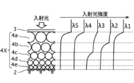
- FIG. 7C is a diagram for explaining the absorption of light including the absorption peak wavelength of each quantum dot layer in the photoelectric conversion layer 4 according to this embodiment.
- FIG. 7D is for explaining the absorption of light including the absorption peak wavelength of each quantum dot layer in the photoelectric conversion layer 4X in which the stacking order of the quantum dot layers is different from that of the photoelectric conversion layer 4 according to the present embodiment. It is a diagram.
- the graphs on the right side of FIGS. 7C and 7D schematically show changes in the intensity of light with wavelengths from ⁇ 1 to ⁇ 5 with respect to light with wavelengths from ⁇ 1 to ⁇ 5 incident on the photoelectric conversion layer 4 from the second electrode 3 side. shown in The vertical direction of the graphs on the right side of FIGS.
- 7C and 7D indicates the positions of the stacked quantum dot layers in the stacking direction.
- different offsets are added to the intensities of light with wavelengths ⁇ 1 to ⁇ 5 for ease of viewing.
- the absorption wavelength region on the short wavelength side of the absorption peak wavelength of a certain quantum dot layer overlaps with the absorption peak of another quantum dot layer with a shorter absorption peak wavelength.
- the absorption wavelength region on the shorter wavelength side than ⁇ 1 of the first quantum dot layer 4a having the longest absorption peak wavelength ⁇ 1 is the absorption peak wavelength ⁇ 2 of the second quantum dot layer 4b to the fifth quantum dot layer 4e. overlaps with ⁇ 5. That is, the light of the absorption peak wavelength of the quantum dot layer having the relatively short wavelength absorption peak is absorbed by the quantum dot layer having the relatively long wavelength absorption peak.
- the quantum dot layers are stacked so that the particle diameter decreases in order from the quantum dot layer closer to the first electrode 2, so that the absorption peak wavelength of each quantum dot layer is It becomes longer in order from ⁇ 5 to ⁇ 1. Therefore, when light containing wavelengths from ⁇ 1 to ⁇ 5 is incident from the second electrode 3 side, the light of the absorption peak wavelength of each quantum dot layer is hardly absorbed by the other quantum dot layers, and the light intensity at the time of incidence is It reaches each quantum dot layer and is absorbed. As a result, pairs of electrons and holes tend to be generated evenly throughout the photoelectric conversion layer 4 .
- the first quantum dot layer 4a to the fifth quantum dot layer 4e are laminated in the reverse order of the photoelectric conversion layer 4.
- the absorption peak wavelength of each quantum dot layer ranges from ⁇ 1 to ⁇ 5 from the light incident side. shorter in order.
- the light of the absorption peak wavelength of each quantum dot layer is the first quantum dot layer 4a having the largest particle diameter, that is, the absorption peak It is absorbed by the first quantum dot layer 4a having a long wavelength.
- the first quantum dot layer 4a which has the longest absorption peak wavelength, exhibits high light absorption even for light with wavelengths ⁇ 2 to ⁇ 5, which are shorter than the absorption peak wavelength ⁇ 1.
- the first quantum dot layer 4a absorbs most of the incident light with wavelengths ⁇ 4 and ⁇ 5.
- the quantum dot layer closer to the second electrode 3 has a longer absorption peak wavelength and a wider wavelength range for absorption, so the quantum dots closer to the first electrode 2
- the intensity of light incident on a layer decreases, and the amount of light absorbed decreases.
- pairs of electrons and holes generated by light incidence are concentrated in the quantum dot layer near the second electrode 3, and carriers are generated at a high concentration, so electrons and holes recombine. As a result, the sensitivity of the photoelectric conversion element decreases.
- the holes generated in the quantum dot layer near the second electrode 3 are far from the first electrode 2 that collects the holes, so they are likely to be deactivated before being collected by the first electrode 2 as signal charges. . Therefore, holes, which are signal charges, are not efficiently collected.
- the photoelectric conversion layer 4 by stacking the quantum dot layers so that the particle diameter becomes smaller in order from the quantum dot layer closer to the first electrode 2, in the vicinity of the first electrode 2 Photoelectric conversion is more likely to occur.
- the incident light when light is incident from the second electrode 3 side, the incident light can be used more effectively. Therefore, the sensitivity of the photoelectric conversion element can be improved.
- the n-layer quantum dot layers have mutually different bandgap energies (that is, absorption peak wavelengths), the sensitivity wavelength region of the photoelectric conversion element can be expanded.
- the quantum dot layer near the first electrode 2 is smaller than the bandgap energy of the quantum dot layer close to the second electrode 3, photoelectric conversion is likely to occur even in the quantum dot layer close to the first electrode 2 for the above reason, and the photoelectric conversion element Sensitivity can be improved.
- quantum dots with the smallest particle size have the largest bandgap energy. Therefore, as shown in FIG. 7A, in the case of a laminated structure in which the particle diameter of the quantum dots contained in the fifth quantum dot layer 4e closest to the second electrode 3 is the smallest, the Fermi level of the second electrode 3 and the energy at the top of the valence band of the fifth quantum dot layer 4e becomes the largest. Therefore, in order to use holes as signal charges, when a voltage is applied so that the second electrode 3 has a positive potential with respect to the first electrode 2 , holes are transferred from the second electrode 3 to the photoelectric conversion layer 4 . can suppress the dark current that is injected and collected in the first electrode 2 .
- the bandgap energy of the quantum dot layers closer to the first electrode 2 becomes smaller. Therefore, if each quantum dot layer is configured so that the energy at the bottom of the conduction band becomes smaller for the quantum dot layer closer to the first electrode 2 so as to satisfy the above formula (7), in the direction toward the first electrode 2, The energy at the top of the valence band of each quantum dot layer changes so as to decrease with a larger change width than the change in the energy at the bottom of the conduction band.
- the potential gradient for holes, which are signal charges, in the direction toward the first electrode 2 is the potential gradient of electrons, which are charges of the opposite polarity of the signal charges, in the direction toward the second electrode 3. larger than the potential gradient. Also, the difference between the potential gradient for holes and the potential gradient for electrons tends to increase. Therefore, it is possible to realize a photoelectric conversion element that collects signal charges at a higher speed and has a higher response to signal charges.
- n-layered quantum dot layers are stacked so as not to form an energy barrier for the transport of at least one of holes and electrons. Therefore, it is possible to suppress accumulation of charges generated by photoelectric conversion at the interface between specific quantum dot layers. Therefore, the sensitivity of the photoelectric conversion element can be improved.
- the quantum dot layer near the first electrode 2 The bandgap energy is smaller than that of the quantum dot layer closer to the second electrode 3 .
- the light of the absorption peak wavelength of the quantum dot layer closer to the first electrode 2 out of the two adjacent quantum dot layers is less likely to be absorbed by the quantum dot layer closer to the second electrode 3 .
- photoelectric conversion tends to occur in the quantum dot layer near the first electrode 2, and the first electrode 2 tends to collect signal charges. Therefore, the sensitivity of the photoelectric conversion element can be improved.
- the n quantum dot layers include a combination of two adjacent quantum dot layers with different bandgap energies, quantum dot layers with different absorption peak wavelengths are stacked. Therefore, the sensitivity wavelength region of the photoelectric conversion element can be expanded.
- Embodiment 5 Next, Embodiment 5 will be described.
- the cases where holes are used as signal charges have been explained, but in the fifth embodiment, the case where electrons are used as signal charges will be explained.
- electrons When electrons are used as signal charges, it can be realized by changing the energy band of each layer in the photoelectric conversion elements according to the first to fourth embodiments.
- the photoelectric conversion element according to Embodiment 5 the energy band of the n-layer quantum dot layer included in the photoelectric conversion layer 4 and the positions of the electron-blocking layer 5 and the hole-blocking layer 6 are exchanged. is the same as the photoelectric conversion element according to the first embodiment.
- the differences from the first to fourth embodiments will be mainly described, and the description of the common points will be omitted or simplified.
- FIG. 8 is a diagram showing an example of an energy diagram of the photoelectric conversion layer according to this embodiment.
- FIG. 8 shows an example of an energy diagram when five quantum dot layers containing quantum dots of the same constituent element with different particle sizes are stacked.
- FIG. 8 also schematically shows the particle size of the quantum dots contained in each quantum dot layer above the energy band of each quantum dot layer.
- the first electrode 2 is an electron collection electrode that collects electrons generated in the photoelectric conversion layer 4 as signal charges.
- the second electrode 3 is a hole collection electrode that collects holes as charges of the polarity of signal charges generated in the photoelectric conversion layer 4 .
- the bias voltage applied to the first electrode 2 and the second electrode 3 is such that, of pairs of electrons and holes generated in the photoelectric conversion layer 4, holes move to the second electrode 3 and electrons move to the first electrode.
- Polarity is determined to move to 2.
- a bias voltage is applied such that the potential of the second electrode 3 becomes negative with respect to the first electrode 2 .
- the first electrode 2 collects electrons, which are signal charges
- the second electrode 3 collects holes, which are charges of opposite polarity to the signal charges, and discharges them to the outside, for example.
- the work function of the second electrode 3 larger than the work function of the first electrode 2, the first electrode 2 collects electrons under the condition that there is no potential difference between the first electrode and the second electrode.
- Two electrodes 3 may eject holes.
- n Layers of quantum dot layers are stacked.
- n quantum dot layers By stacking n quantum dot layers so that this relationship is established at the interface between all two adjacent quantum dot layers of the n quantum dot layers, both electrons and holes generated by photoelectric conversion Accumulation at interfaces between specific quantum dot layers can be suppressed. Therefore, sensitivity and response speed can be improved.
- the energy relationship at the interface between each of the n quantum dot layers and the adjacent quantum dot layer is Both the following equations (13) and (14) are satisfied.
- equations (13) and (14) can be converted to equations (15) and (16), respectively.
- dark current can be suppressed by providing an energy barrier ⁇ E g,i at the interface between two adjacent quantum dot layers. Therefore, in a structure in which n quantum dot layers are stacked, the energy barrier ⁇ E g,i at the interface between each of the n quantum dot layers and the adjacent quantum dot layer is expressed by the following formula ( 17) is satisfied.
- Equation (17) can be converted to Equation (18).
- the particle diameter of the quantum dots included in each of the n-layer quantum dot layers is close to that of the first electrode 2. It becomes smaller in order from the layer.
- the quantum dots included in each quantum dot layer are quantum dots of the same constituent element. The bandgap energy increases in order from the quantum dot layer closer to the first electrode 2 .
- the bandgap energy of the quantum dot layer closer to the first electrode 2 is the quantum dot layer closer to the second electrode 3 less than the bandgap energy of
- the bandgap energy of the quantum dot layer near the first electrode 2 is the quantum dot layer near the second electrode 3. It may be equal to or higher than the bandgap energy of the dot layer.
- each quantum dot layer has the bandgap energy as described above, the absorption peak wavelength of each of the n quantum dot layers becomes shorter in order from the quantum dot layer closer to the first electrode 2 .
- the bandgap energy of the quantum dot layers closer to the first electrode 2 becomes smaller. Therefore, if each quantum dot layer is configured such that the closer the quantum dot layer is to the second electrode 3, the lower the energy of the valence band upper end so as to satisfy the expression (13), the energy of the lower end of the conduction band of each quantum dot layer is changes in the direction toward the second electrode 3 with a larger change width than the change in energy at the top of the valence band.
- the potential gradient for electrons, which are signal charges, in the direction toward the first electrode 2 is the same as that for holes, which are charges of the opposite polarity of the signal charges, in the direction toward the second electrode 3. larger than the potential gradient. Also, the difference between the potential gradient for electrons and the potential gradient for holes tends to increase. Therefore, it is possible to realize a photoelectric conversion element in which signal charges are collected at a higher speed and the responsiveness of signal charges is improved.
- the photoelectric conversion element according to the present embodiment includes the electron-blocking layer 5 and the hole-blocking layer 6, the electron-blocking layer 5 and the hole-blocking layer are different from the structure of the photoelectric conversion element 10B shown in FIG. 2A. 6, a photoelectric conversion element including the electron blocking layer 5 and the hole blocking layer 6 can be realized. That is, by placing the hole blocking layer 6 between the first electrode 2 and the photoelectric conversion layer 4 and placing the electron blocking layer 5 between the second electrode 3 and the photoelectric conversion layer 4, the electron blocking layer 5 and a hole blocking layer 6 can be realized.
- the electron affinity ⁇ EBL of the electron blocking layer 5 is the fifth quantum dot layer 4e closest to the electron blocking layer 5 among the five quantum dot layers. is equal to or less than the electron affinity ⁇ 5 of Further, for example, the ionization potential I EBL of the electron blocking layer 5 is set higher than the ionization potential I 5 of the fifth quantum dot layer 4 e so as not to hinder the conduction of holes from the fifth quantum dot layer 4 e to the second electrode 3 . The value is equal to or smaller than the upper limit of 0.5 eV.
- the ionization potential I HBL of the hole blocking layer 6 is set to the first quantum dot layer closest to the hole blocking layer 6 among the five quantum dot layers. It is equal to or greater than the ionization potential I1 of the dot layer 4a. Further, for example, the electron affinity ⁇ HBL of the hole blocking layer 6 is equal to the electron affinity ⁇ 1 of the first quantum dot layer 4a so as not to hinder the conduction of electrons from the first quantum dot layer 4a to the first electrode 2 . Equal to or greater than.
- the sensitivity wavelength region is expanded and It is possible to achieve both improvement in sensitivity.
- Embodiment 6 Next, Embodiment 6 will be described.
- an imaging device using the photoelectric conversion elements according to Embodiments 1 to 5 will be described.
- the differences from the first to fifth embodiments will be mainly described, and the description of the common points will be omitted or simplified.
- FIG. 9 is a diagram showing an example of the circuit configuration of the imaging device 100 according to this embodiment.
- An imaging device 100 shown in FIG. 9 has a plurality of pixels 20 and peripheral circuits.
- the peripheral circuit includes a voltage supply circuit 30 that supplies a predetermined voltage to each pixel 20 .
- the pixels 20 form a photosensitive region, a so-called pixel region, by being arranged one-dimensionally or two-dimensionally on the semiconductor substrate.
- the pixels 20 are arranged in rows and columns.
- row direction and column direction refer to directions in which rows and columns extend, respectively. That is, the vertical direction on the paper surface of FIG. 9 is the column direction, and the horizontal direction is the row direction.
- FIG. 9 shows four pixels 20 arranged in a 2 ⁇ 2 matrix.
- the number of pixels 20 shown in FIG. 9 is merely an example for explanation, and the number of pixels 20 is not limited to four. If the pixels 20 are arranged one-dimensionally, the imaging device 100 is a line sensor.
- Each of the plurality of pixels 20 has a photoelectric conversion unit 10C and a signal detection circuit 40 that detects the signal generated by the photoelectric conversion unit 10C.
- the signal detection circuit 40 is an example of a signal readout circuit.
- the photoelectric conversion part 10C includes a first electrode 2, a second electrode 3, and a photoelectric conversion layer 4 arranged therebetween.
- the photoelectric conversion unit 10C is composed of the photoelectric conversion element according to any one of Embodiments 1 to 5, for example.
- the photoelectric conversion unit 10C is composed of a photoelectric conversion element in which the first electrode 2 collects holes as signal charges, like the photoelectric conversion element according to any one of Embodiments 1 to 4. An example will be mainly described.
- the photoelectric conversion unit 10C may be composed of a photoelectric conversion element in which the first electrode 2 collects electrons as signal charges, like the photoelectric conversion element according to the fifth embodiment. Further, the photoelectric conversion section 10C may include the electron blocking layer 5 and the hole blocking layer 6 like the photoelectric conversion element 10B described above.
- the first electrode 2 functions as a charge collector.
- a signal detection circuit 40 is connected to the first electrode 2 .
- the second electrode 3 is connected to the voltage supply circuit 30 via the accumulation control line 22 .
- a predetermined bias voltage is applied to the second electrode 3 via the accumulation control line 22 during operation of the imaging device 100 .
- the first electrode 2 is a pixel electrode that collects signal charges
- the second electrode 3 is a counter electrode facing the pixel electrode.
- the photoelectric conversion unit 10C is configured so that the first electrode 2 collects holes (in other words, positive charges) as signal charges among pairs of electrons and holes generated by photoelectric conversion. Holes can be collected by the first electrode 2 by controlling the potential of the second electrode 3 using the bias voltage generated by the voltage supply circuit 30 .
- the voltage supply circuit 30 supplies a voltage to the second electrode 3 via the accumulation control line 22 so that the second electrode 3 has a positive potential with respect to the first electrode 2 . Specifically, a voltage of about 10 V, for example, is applied to the accumulation control line 22 so that the potential of the second electrode 3 is higher than that of the first electrode 2 .
- the voltage supply circuit 30 applies a voltage that makes the second electrode 3 negative with respect to the first electrode 2 via the accumulation control line 22 to the second electrode 2 . supply to the electrode 3;
- the signal detection circuit 40 includes an amplification transistor 42, an address transistor 44, and a reset transistor 46.
- the amplification transistor 42 is also called a charge detection transistor
- the address transistor 44 is also called a row selection transistor.
- amplification transistor 42 and address transistor 44 are field effect transistors (FETs) formed in a semiconductor substrate.
- FETs field effect transistors
- Amplifying transistor 42, address transistor 44 and reset transistor 46 have a control terminal, an input terminal and an output terminal.
- a control terminal is, for example, a gate.
- the input terminal is one of the drain and the source, typically the drain.
- the output terminal is the other of the drain and source, typically the source.
- semiconductor substrate in this specification is not limited to a substrate whose entirety is a semiconductor, and may be an insulating substrate or the like provided with a semiconductor layer on the surface on which the photosensitive region is formed.
- An example of a semiconductor substrate is a p-type silicon substrate.
- one of the input terminal and output terminal of the amplification transistor 42 and one of the input terminal and output terminal of the address transistor 44 are connected.
- a control terminal of the amplification transistor 42 is electrically connected to the first electrode 2 of the photoelectric conversion section 10C.
- Signal charges collected by the first electrode 2 are stored in the charge storage node 41 between the first electrode 2 and the gate of the amplification transistor 42 .
- the signal charges are holes.
- the charge storage node 41 is an example of a charge storage section and is also called a "floating diffusion node". Note that when the photoelectric conversion unit 10C is composed of the photoelectric conversion element according to Embodiment 5, the signal charges may be electrons.
- a voltage corresponding to the signal charge accumulated in the charge accumulation node 41 is applied to the gate of the amplification transistor 42 .
- Amplification transistor 42 amplifies this voltage. That is, the amplification transistor 42 amplifies the signal generated by the photoelectric conversion unit 10C.
- the voltage amplified by the amplification transistor 42 is selectively read out through the address transistor 44 as a signal voltage.
- One of the source and drain of the reset transistor 46 is connected to the charge storage node 41 , and one of the source and drain of the reset transistor 46 is electrically connected to the first electrode 2 .
- the reset transistor 46 resets the signal charges accumulated in the charge accumulation node 41 . In other words, the reset transistor 46 resets the potential of the gate of the amplification transistor 42 and the first electrode 2 .
- the imaging device 100 includes a power line 23, a vertical signal line 24, an address signal line 25, and a reset signal line 26. These lines are connected to each pixel 20 .
- the power supply line 23 is connected to one of the source and drain of the amplification transistor 42 and supplies a predetermined power supply voltage to each pixel 20 .
- the power line 23 functions as a source follower power supply.
- the vertical signal line 24 is connected to one of the source and drain of the address transistor 44 that is not connected to the source or drain of the amplification transistor 42 .
- the address signal line 25 is connected to the gate of the address transistor 44 .
- the reset signal line 26 is connected to the gate of the reset transistor 46 .
- the peripheral circuits of the imaging device 100 include a vertical scanning circuit 52, a horizontal signal readout circuit 54, a plurality of column signal processing circuits 56, a plurality of load circuits 58, and a plurality of inverting amplifiers 59.
- the vertical scanning circuit 52 is also called a "row scanning circuit”
- the horizontal signal readout circuit 54 is also called a “column scanning circuit”
- the column signal processing circuit 56 is also called a "row signal storage circuit”.
- a column signal processing circuit 56, a load circuit 58 and an inverting amplifier 59 are provided corresponding to each column of the plurality of pixels 20 arranged in row and column directions.
- Each of the column signal processing circuits 56 is electrically connected to the pixels 20 arranged in each column through the vertical signal lines 24 corresponding to each column of the plurality of pixels 20 .
- a plurality of column signal processing circuits 56 are electrically connected to the horizontal signal readout circuit 54 .
- Each load circuit 58 is electrically connected to each vertical signal line 24 , and the load circuit 58 and the amplification transistor 42 form a source follower circuit.
- the vertical scanning circuit 52 is connected to the address signal line 25 and the reset signal line 26.
- the vertical scanning circuit 52 applies a row selection signal to the gate of the address transistor 44 via the address signal line 25 to control on/off of the address transistor 44 .
- a row to be read is scanned and selected by sending a row selection signal for each address signal line 25 .
- a signal voltage is read out to the vertical signal line 24 from the pixels 20 in the selected row.
- the vertical scanning circuit 52 applies a reset signal to the gate of the reset transistor 46 via the reset signal line 26 to control on/off of the reset transistor 46 .
- By sending a row selection signal to each reset signal line 26 a row of pixels 20 to be reset is selected. In this manner, the vertical scanning circuit 52 selects a plurality of pixels 20 on a row-by-row basis, reads the signal voltage, and resets the potential of the first electrode 2 .
- a signal voltage read from the pixel 20 selected by the vertical scanning circuit 52 is sent to the column signal processing circuit 56 via the vertical signal line 24 .
- the column signal processing circuit 56 performs noise suppression signal processing typified by correlated double sampling, analog-to-digital conversion (AD conversion), and the like.
- the horizontal signal readout circuit 54 sequentially reads signals from the plurality of column signal processing circuits 56 to a horizontal common signal line (not shown).
- the vertical scanning circuit 52 may partially include the voltage supply circuit 30 described above.
- the voltage supply circuit 30 may have electrical connection with the vertical scanning circuit 52 .
- a bias voltage may be applied to the second electrodes 3 via the vertical scanning circuit 52 .
- a plurality of inverting amplifiers 59 are provided corresponding to each column.
- a negative input terminal of the inverting amplifier 59 is connected to the corresponding vertical signal line 24 .
- the output terminal of the inverting amplifier 59 is connected to each pixel 20 in the corresponding column via the feedback line 27 provided corresponding to each column.
- the feedback line 27 is connected to the one of the source and drain of the reset transistor 46 that is not connected to the charge storage node 41 (for example, the drain). Therefore, inverting amplifier 59 receives the output of address transistor 44 at its negative terminal when address transistor 44 and reset transistor 46 are in a conducting state.
- the positive input terminal of the inverting amplifier 59 is applied with a reset reference voltage from a power supply (not shown).
- the inverting amplifier 59 performs a feedback operation so that the gate voltage of the amplification transistor 42 becomes a predetermined feedback voltage.
- Feedback voltage means the output voltage of the inverting amplifier 59 .
- the output voltage of the inverting amplifier 59 is, for example, 0V or a positive voltage near 0V.
- Inverting amplifier 59 may also be referred to as a "feedback amplifier".
- FIG. 10 is a cross-sectional view schematically showing the device structure of the pixel 20 in the imaging device 100 according to this embodiment.
- the pixel 20 includes a semiconductor substrate 62 that supports the photoelectric conversion section 10C.
- the semiconductor substrate 62 is, for example, a silicon substrate.
- the photoelectric conversion section 10C is arranged above the semiconductor substrate 62.
- light enters the photoelectric conversion unit 10C from above the photoelectric conversion unit 10C. That is, light enters from the second electrode 3 side of the photoelectric conversion unit 10C.
- interlayer insulating layers 63A, 63B, and 63C are laminated on a semiconductor substrate 62, and a first electrode 2, a photoelectric conversion layer 4, and a second electrode 3 are laminated in this order on the interlayer insulating layer 63C. ing.
- the first electrodes 2 are partitioned for each pixel, and the first electrodes 2 are spatially separated between two adjacent pixels 20, so that the two adjacent first electrodes 2 are electrically are separated into Moreover, the photoelectric conversion layer 4 and the second electrode 3 may be formed so as to straddle a plurality of pixels 20 .
- An amplification transistor 42, an address transistor 44 and a reset transistor 46 are formed on the semiconductor substrate 62.
- FIG. 1 An amplification transistor 42, an address transistor 44 and a reset transistor 46 are formed on the semiconductor substrate 62.
- the amplification transistor 42 includes impurity regions 62a and 62b formed in a semiconductor substrate 62, a gate insulating layer 42g located on the semiconductor substrate 62, and a gate electrode 42e located on the gate insulating layer 42g.
- Impurity regions 62 a and 62 b function as the drain or source of amplifying transistor 42 .
- Impurity regions 62a, 62b and impurity regions 62c, 62d, 62e which will be described later, are, for example, n-type impurity regions.
- the address transistor 44 includes impurity regions 62a and 62c formed in a semiconductor substrate 62, a gate insulating layer 44g located on the semiconductor substrate 62, and a gate electrode 44e located on the gate insulating layer 44g. Impurity regions 62 a and 62 c function as the drain or source of address transistor 44 .
- the amplification transistor 42 and the address transistor 44 share the impurity region 62a, so that the source (or drain) of the amplification transistor 42 and the drain (or source) of the address transistor 44 are electrically connected.
- the reset transistor 46 includes impurity regions 62d and 62e formed in the semiconductor substrate 62, a gate insulating layer 46g located on the semiconductor substrate 62, and a gate electrode 46e located on the gate insulating layer 46g. Impurity regions 62 d and 62 e function as the drain or source of reset transistor 46 .
- Element isolation regions 62 s are provided in the semiconductor substrate 62 between the pixels 20 adjacent to each other and between the amplification transistor 42 and the reset transistor 46 . Pixels 20 adjacent to each other are electrically isolated by the element isolation region 62s. Further, by providing the element isolation region 62s between the pixels 20 adjacent to each other, leakage of the signal charge accumulated in the charge accumulation node 41 is suppressed.
- a contact plug 65A connected to the impurity region 62d of the reset transistor 46, a contact plug 65B connected to the gate electrode 42e of the amplification transistor 42, and the contact plug 65A and the contact plug 65B are connected.
- a wiring 66A is formed.
- the impurity region 62 d (for example, the drain) of the reset transistor 46 is electrically connected to the gate electrode 42 e of the amplification transistor 42 .
- a plug 67A and wiring 68A are further formed in the interlayer insulating layer 63A.
- a plug 67B and a wiring 68B are formed in the interlayer insulating layer 63B, and a plug 67C is formed in the interlayer insulating layer 63C, whereby the wiring 66A and the first electrode 2 are electrically connected.
- Contact plug 65A, contact plug 65B, wiring 66A, plug 67A, wiring 68A, plug 67B, wiring 68B, and plug 67C are typically made of metal.
- a protective layer 72 is arranged on the second electrode 3 .
- This protective layer 72 is not a substrate arranged to support the photoelectric conversion section 10C.
- the protective layer 72 is a layer for protecting the photoelectric conversion section 10C and insulating it from others.
- the protective layer 72 may be highly translucent at wavelengths absorbed by the photoelectric conversion layer 4 .
- the material of the protective layer 72 may be any insulator having translucency, such as SiON or AlO, for example.
- microlenses 74 may be arranged on the protective layer 72 .
- the photoelectric conversion unit 10C is an example of a photoelectric conversion element, and is composed of the photoelectric conversion element according to any one of Embodiments 1 to 5.
- the photoelectric conversion unit 10C has, for example, the same structure as the photoelectric conversion element 10A described above, as shown in FIG.
- the second electrode 3 is arranged above the photoelectric conversion layer 4 , in other words, on the light incident side of the imaging device 100 with respect to the photoelectric conversion layer 4 . Light enters the photoelectric conversion layer 4 through the second electrode 3 .
- the photoelectric conversion section 10C may have the same structure as the photoelectric conversion element 10B described above, and one of the electron blocking layer 5 and the hole blocking layer 6 of the photoelectric conversion element 10B described above is You may have the structure which is not provided.
- the signal detection circuit 40 is connected to the first electrode 2 and the voltage supply circuit 30 supplies voltage to the second electrode 3 via the accumulation control line 22 .
- the imaging device 100 as described above can be manufactured using a general semiconductor manufacturing process.
- a silicon substrate is used as the semiconductor substrate 62, it can be manufactured using various silicon semiconductor processes.
- the photoelectric conversion element according to any one of Embodiments 1 to 5 is used in the imaging device 100 according to the present embodiment, both the expansion of the sensitivity wavelength range and the improvement of the sensitivity of the imaging device 100 are achieved. be able to. Therefore, the imaging device 100 can image light in a wide wavelength range with low noise.
- n quantum dot layers having mutually different bandgap energies and absorption wavelengths by changing the particle diameter of the quantum dots in each quantum dot layer was mainly described. Not exclusively. By changing the constituent elements of the quantum dots in each quantum dot layer, n quantum dot layers having different bandgap energies and absorption wavelengths may be stacked.
- the photoelectric conversion element according to the present disclosure may be used in solar cells by extracting electric charges generated by light as energy. Further, the photoelectric conversion element according to the present disclosure may be used as an optical sensor by extracting electric charge generated by light as a signal.
- the photoelectric conversion element and imaging device are applicable to photodiodes, image sensors, and the like, and are particularly applicable to optical sensing with high sensitivity and low dark current using infrared wavelengths.
- Electron Blocking Layer 6 hole blocking layer 10A, 10B photoelectric conversion element 10C photoelectric conversion unit 20 pixel 22 accumulation control line 23 power supply line 24 vertical signal line 25 address signal line 26 reset signal line 27 feedback line 30 voltage supply circuit 40 signal detection circuit 41 charge accumulation node 42 amplification transistor 42e, 44e, 46e gate electrode 42g, 44g, 46g gate insulating layer 44 address transistor 46 reset transistor 52 vertical scanning circuit 54 horizontal signal readout circuit 56 column signal processing circuit 58 load circuit 59 inverting amplifier 62 semiconductor substrate 62a, 62b, 62c, 62d, 62e impurity region 62s element isolation region 63A, 63B, 63C interlayer insulating layer 65A, 65B contact plug 66A wiring 67A, 67B, 67
Landscapes
- Chemical & Material Sciences (AREA)
- Engineering & Computer Science (AREA)
- Materials Engineering (AREA)
- Organic Chemistry (AREA)
- Crystallography & Structural Chemistry (AREA)
- Inorganic Chemistry (AREA)
- Nanotechnology (AREA)
- Physics & Mathematics (AREA)
- Electromagnetism (AREA)
- Light Receiving Elements (AREA)
Priority Applications (4)
| Application Number | Priority Date | Filing Date | Title |
|---|---|---|---|
| JP2024501027A JPWO2023157531A1 (https=) | 2022-02-16 | 2023-01-17 | |
| EP23756059.4A EP4481835A4 (en) | 2022-02-16 | 2023-01-17 | Photoelectric conversion element and imaging device |
| CN202380017964.4A CN118575285A (zh) | 2022-02-16 | 2023-01-17 | 光电转换元件及摄像装置 |
| US18/782,984 US20240381677A1 (en) | 2022-02-16 | 2024-07-24 | Photoelectric conversion element and imaging apparatus |
Applications Claiming Priority (2)
| Application Number | Priority Date | Filing Date | Title |
|---|---|---|---|
| JP2022022315 | 2022-02-16 | ||
| JP2022-022315 | 2022-02-16 |
Related Child Applications (1)
| Application Number | Title | Priority Date | Filing Date |
|---|---|---|---|
| US18/782,984 Continuation US20240381677A1 (en) | 2022-02-16 | 2024-07-24 | Photoelectric conversion element and imaging apparatus |
Publications (1)
| Publication Number | Publication Date |
|---|---|
| WO2023157531A1 true WO2023157531A1 (ja) | 2023-08-24 |
Family
ID=87578264
Family Applications (1)
| Application Number | Title | Priority Date | Filing Date |
|---|---|---|---|
| PCT/JP2023/001179 Ceased WO2023157531A1 (ja) | 2022-02-16 | 2023-01-17 | 光電変換素子および撮像装置 |
Country Status (5)
| Country | Link |
|---|---|
| US (1) | US20240381677A1 (https=) |
| EP (1) | EP4481835A4 (https=) |
| JP (1) | JPWO2023157531A1 (https=) |
| CN (1) | CN118575285A (https=) |
| WO (1) | WO2023157531A1 (https=) |
Cited By (1)
| Publication number | Priority date | Publication date | Assignee | Title |
|---|---|---|---|---|
| WO2025120799A1 (ja) * | 2023-12-07 | 2025-06-12 | ソニーセミコンダクタソリューションズ株式会社 | 光検出装置および電子機器 |
Families Citing this family (1)
| Publication number | Priority date | Publication date | Assignee | Title |
|---|---|---|---|---|
| WO2022249844A1 (ja) * | 2021-05-24 | 2022-12-01 | パナソニックIpマネジメント株式会社 | 光電変換素子、撮像装置および光電変換素子の駆動方法 |
Citations (5)
| Publication number | Priority date | Publication date | Assignee | Title |
|---|---|---|---|---|
| US20150357534A1 (en) * | 2014-06-09 | 2015-12-10 | The Board Of Trustees Of The Leland Stanford Junior University | Atomic Layer Deposition (ALD) of TiO2 using (Tetrakis(dimethylamino)titanium) TDMAT as an Encapsulation and/or Barrier Layer for ALD PbS |
| US20170025466A1 (en) * | 2015-07-23 | 2017-01-26 | Artilux Corporation | High Efficiency Wide Spectrum Sensor |
| JP2017516320A (ja) * | 2014-05-09 | 2017-06-15 | マサチューセッツ インスティテュート オブ テクノロジー | リガンド交換を介したナノクリスタルのエネルギーレベル修正 |
| US20180254421A1 (en) * | 2015-10-02 | 2018-09-06 | Toyota Motor Europe | All quantum dot based optoelectronic device |
| CN111477644A (zh) * | 2020-03-31 | 2020-07-31 | 东南大学 | 一种近红外/可见光/紫外集成光谱成像器件及成像方法 |
Family Cites Families (2)
| Publication number | Priority date | Publication date | Assignee | Title |
|---|---|---|---|---|
| US9941433B2 (en) * | 2014-12-11 | 2018-04-10 | Vadient Optics, Llc | Composite quantum-dot materials for photonic detectors |
| JP6298223B2 (ja) * | 2015-08-28 | 2018-03-20 | 京セラ株式会社 | 光電変換装置 |
-
2023
- 2023-01-17 WO PCT/JP2023/001179 patent/WO2023157531A1/ja not_active Ceased
- 2023-01-17 EP EP23756059.4A patent/EP4481835A4/en active Pending
- 2023-01-17 CN CN202380017964.4A patent/CN118575285A/zh active Pending
- 2023-01-17 JP JP2024501027A patent/JPWO2023157531A1/ja active Pending
-
2024
- 2024-07-24 US US18/782,984 patent/US20240381677A1/en active Pending
Patent Citations (5)
| Publication number | Priority date | Publication date | Assignee | Title |
|---|---|---|---|---|
| JP2017516320A (ja) * | 2014-05-09 | 2017-06-15 | マサチューセッツ インスティテュート オブ テクノロジー | リガンド交換を介したナノクリスタルのエネルギーレベル修正 |
| US20150357534A1 (en) * | 2014-06-09 | 2015-12-10 | The Board Of Trustees Of The Leland Stanford Junior University | Atomic Layer Deposition (ALD) of TiO2 using (Tetrakis(dimethylamino)titanium) TDMAT as an Encapsulation and/or Barrier Layer for ALD PbS |
| US20170025466A1 (en) * | 2015-07-23 | 2017-01-26 | Artilux Corporation | High Efficiency Wide Spectrum Sensor |
| US20180254421A1 (en) * | 2015-10-02 | 2018-09-06 | Toyota Motor Europe | All quantum dot based optoelectronic device |
| CN111477644A (zh) * | 2020-03-31 | 2020-07-31 | 东南大学 | 一种近红外/可见光/紫外集成光谱成像器件及成像方法 |
Non-Patent Citations (4)
| Title |
|---|
| BO HOU: "ACS Energy Lettes", vol. 1, 2016, AMERICAN CHEMICAL SOCIETY, article "Highly Monodispersed PbS Quantum Dots for Outstanding Cascaded-Junction Solar Cells", pages: 834 - 839 |
| HOU BO, CHO YULJAE, KIM BYUNG SUNG, HONG JOHN, PARK JONG BAE, AHN SE JIN, SOHN JUNG INN, CHA SEUNGNAM, KIM JONG MIN: "Highly Monodispersed PbS Quantum Dots for Outstanding Cascaded-Junction Solar Cells", ACS ENERGY LETTERS, ACS, AMERICAN CHEMICAL SOCIETY, vol. 1, no. 4, 14 October 2016 (2016-10-14), American Chemical Society, pages 834 - 839, XP093085996, ISSN: 2380-8195, DOI: 10.1021/acsenergylett.6b00294 * |
| PATRICK R. BROWN ET AL.: "ACS Nano", vol. 8, 2014, AMERICAN CHEMICAL SOCIETY, article "Energy Level Modification in Lead Sulfide Quantum Dot Thin Films through Ligand Exchange", pages: 5863 - 5872 |
| See also references of EP4481835A4 |
Cited By (1)
| Publication number | Priority date | Publication date | Assignee | Title |
|---|---|---|---|---|
| WO2025120799A1 (ja) * | 2023-12-07 | 2025-06-12 | ソニーセミコンダクタソリューションズ株式会社 | 光検出装置および電子機器 |
Also Published As
| Publication number | Publication date |
|---|---|
| EP4481835A1 (en) | 2024-12-25 |
| US20240381677A1 (en) | 2024-11-14 |
| EP4481835A4 (en) | 2025-05-14 |
| JPWO2023157531A1 (https=) | 2023-08-24 |
| CN118575285A (zh) | 2024-08-30 |
Similar Documents
| Publication | Publication Date | Title |
|---|---|---|
| Xu et al. | Photodetectors based on solution-processable semiconductors: Recent advances and perspectives | |
| WO2022244575A1 (ja) | 光電変換素子および撮像装置 | |
| Ghosh et al. | Recent advances in perovskite/2D materials based hybrid photodetectors | |
| JP7199039B2 (ja) | 撮像装置 | |
| JP2019009427A (ja) | 光検出素子 | |
| US20240381677A1 (en) | Photoelectric conversion element and imaging apparatus | |
| CN104956483A (zh) | 使用溶液处理pbs光探测器的新型ir图像传感器 | |
| CN108695356A (zh) | 摄像装置 | |
| CN113454795A (zh) | 用于显示器下指纹和手势传感器的具有半导体活性层的光检测器 | |
| JPWO2020170703A1 (ja) | 撮像装置およびその駆動方法 | |
| US20220238576A1 (en) | Imaging device | |
| US12101949B2 (en) | Photoelectric conversion element, electronic device, and light-emitting device | |
| JP7713649B2 (ja) | 撮像装置および駆動方法 | |
| US11777050B2 (en) | Optical sensor | |
| US20240065013A1 (en) | Photoelectric conversion element, imaging apparatus, and method for driving photoelectric conversion element | |
| WO2020080072A1 (ja) | 光電変換素子およびイメージセンサ | |
| CN112673483A (zh) | 摄像装置 | |
| US20250393385A1 (en) | Photoelectric conversion element and imaging device | |
| CN121398179A (zh) | 一种感光像素单元以及图像传感器 | |
| JP2026032297A (ja) | 光電変換素子および撮像装置 | |
| WO2026087867A1 (en) | Direct x-ray detection device and a method of making such a device |
Legal Events
| Date | Code | Title | Description |
|---|---|---|---|
| 121 | Ep: the epo has been informed by wipo that ep was designated in this application |
Ref document number: 23756059 Country of ref document: EP Kind code of ref document: A1 |
|
| WWE | Wipo information: entry into national phase |
Ref document number: 202380017964.4 Country of ref document: CN |
|
| ENP | Entry into the national phase |
Ref document number: 2024501027 Country of ref document: JP Kind code of ref document: A |
|
| WWE | Wipo information: entry into national phase |
Ref document number: 2023756059 Country of ref document: EP |
|
| NENP | Non-entry into the national phase |
Ref country code: DE |
|
| ENP | Entry into the national phase |
Ref document number: 2023756059 Country of ref document: EP Effective date: 20240916 |