WO2023157502A1 - 配線回路基板およびその製造方法 - Google Patents
配線回路基板およびその製造方法 Download PDFInfo
- Publication number
- WO2023157502A1 WO2023157502A1 PCT/JP2022/048683 JP2022048683W WO2023157502A1 WO 2023157502 A1 WO2023157502 A1 WO 2023157502A1 JP 2022048683 W JP2022048683 W JP 2022048683W WO 2023157502 A1 WO2023157502 A1 WO 2023157502A1
- Authority
- WO
- WIPO (PCT)
- Prior art keywords
- metal support
- coating layer
- forming
- via hole
- layer
- Prior art date
- Legal status (The legal status is an assumption and is not a legal conclusion. Google has not performed a legal analysis and makes no representation as to the accuracy of the status listed.)
- Ceased
Links
Images












Classifications
-
- H—ELECTRICITY
- H05—ELECTRIC TECHNIQUES NOT OTHERWISE PROVIDED FOR
- H05K—PRINTED CIRCUITS; CASINGS OR CONSTRUCTIONAL DETAILS OF ELECTRIC APPARATUS; MANUFACTURE OF ASSEMBLAGES OF ELECTRICAL COMPONENTS
- H05K1/00—Printed circuits
- H05K1/02—Details
- H05K1/0201—Thermal arrangements, e.g. for cooling, heating or preventing overheating
- H05K1/0203—Cooling of mounted components
- H05K1/0207—Cooling of mounted components using internal conductor planes parallel to the surface for thermal conduction, e.g. power planes
-
- H—ELECTRICITY
- H05—ELECTRIC TECHNIQUES NOT OTHERWISE PROVIDED FOR
- H05K—PRINTED CIRCUITS; CASINGS OR CONSTRUCTIONAL DETAILS OF ELECTRIC APPARATUS; MANUFACTURE OF ASSEMBLAGES OF ELECTRICAL COMPONENTS
- H05K1/00—Printed circuits
- H05K1/02—Details
-
- H—ELECTRICITY
- H05—ELECTRIC TECHNIQUES NOT OTHERWISE PROVIDED FOR
- H05K—PRINTED CIRCUITS; CASINGS OR CONSTRUCTIONAL DETAILS OF ELECTRIC APPARATUS; MANUFACTURE OF ASSEMBLAGES OF ELECTRICAL COMPONENTS
- H05K1/00—Printed circuits
- H05K1/02—Details
- H05K1/0201—Thermal arrangements, e.g. for cooling, heating or preventing overheating
- H05K1/0203—Cooling of mounted components
- H05K1/0204—Cooling of mounted components using means for thermal conduction connection in the thickness direction of the substrate
- H05K1/0206—Cooling of mounted components using means for thermal conduction connection in the thickness direction of the substrate by printed thermal vias
-
- H—ELECTRICITY
- H05—ELECTRIC TECHNIQUES NOT OTHERWISE PROVIDED FOR
- H05K—PRINTED CIRCUITS; CASINGS OR CONSTRUCTIONAL DETAILS OF ELECTRIC APPARATUS; MANUFACTURE OF ASSEMBLAGES OF ELECTRICAL COMPONENTS
- H05K1/00—Printed circuits
- H05K1/02—Details
- H05K1/03—Use of materials for the substrate
- H05K1/05—Insulated conductive substrates, e.g. insulated metal substrate
-
- H—ELECTRICITY
- H05—ELECTRIC TECHNIQUES NOT OTHERWISE PROVIDED FOR
- H05K—PRINTED CIRCUITS; CASINGS OR CONSTRUCTIONAL DETAILS OF ELECTRIC APPARATUS; MANUFACTURE OF ASSEMBLAGES OF ELECTRICAL COMPONENTS
- H05K1/00—Printed circuits
- H05K1/02—Details
- H05K1/03—Use of materials for the substrate
- H05K1/05—Insulated conductive substrates, e.g. insulated metal substrate
- H05K1/056—Insulated conductive substrates, e.g. insulated metal substrate the metal substrate being covered by an organic insulating layer
-
- H—ELECTRICITY
- H05—ELECTRIC TECHNIQUES NOT OTHERWISE PROVIDED FOR
- H05K—PRINTED CIRCUITS; CASINGS OR CONSTRUCTIONAL DETAILS OF ELECTRIC APPARATUS; MANUFACTURE OF ASSEMBLAGES OF ELECTRICAL COMPONENTS
- H05K1/00—Printed circuits
- H05K1/02—Details
- H05K1/11—Printed elements for providing electric connections to or between printed circuits
-
- H—ELECTRICITY
- H05—ELECTRIC TECHNIQUES NOT OTHERWISE PROVIDED FOR
- H05K—PRINTED CIRCUITS; CASINGS OR CONSTRUCTIONAL DETAILS OF ELECTRIC APPARATUS; MANUFACTURE OF ASSEMBLAGES OF ELECTRICAL COMPONENTS
- H05K1/00—Printed circuits
- H05K1/02—Details
- H05K1/11—Printed elements for providing electric connections to or between printed circuits
- H05K1/115—Via connections; Lands around holes or via connections
-
- H—ELECTRICITY
- H05—ELECTRIC TECHNIQUES NOT OTHERWISE PROVIDED FOR
- H05K—PRINTED CIRCUITS; CASINGS OR CONSTRUCTIONAL DETAILS OF ELECTRIC APPARATUS; MANUFACTURE OF ASSEMBLAGES OF ELECTRICAL COMPONENTS
- H05K1/00—Printed circuits
- H05K1/18—Printed circuits structurally associated with non-printed electric components
- H05K1/181—Printed circuits structurally associated with non-printed electric components associated with surface mounted components
-
- H—ELECTRICITY
- H05—ELECTRIC TECHNIQUES NOT OTHERWISE PROVIDED FOR
- H05K—PRINTED CIRCUITS; CASINGS OR CONSTRUCTIONAL DETAILS OF ELECTRIC APPARATUS; MANUFACTURE OF ASSEMBLAGES OF ELECTRICAL COMPONENTS
- H05K3/00—Apparatus or processes for manufacturing printed circuits
- H05K3/40—Forming printed elements for providing electric connections to or between printed circuits
-
- H—ELECTRICITY
- H05—ELECTRIC TECHNIQUES NOT OTHERWISE PROVIDED FOR
- H05K—PRINTED CIRCUITS; CASINGS OR CONSTRUCTIONAL DETAILS OF ELECTRIC APPARATUS; MANUFACTURE OF ASSEMBLAGES OF ELECTRICAL COMPONENTS
- H05K3/00—Apparatus or processes for manufacturing printed circuits
- H05K3/40—Forming printed elements for providing electric connections to or between printed circuits
- H05K3/4038—Through-connections; Vertical interconnect access [VIA] connections
-
- H—ELECTRICITY
- H05—ELECTRIC TECHNIQUES NOT OTHERWISE PROVIDED FOR
- H05K—PRINTED CIRCUITS; CASINGS OR CONSTRUCTIONAL DETAILS OF ELECTRIC APPARATUS; MANUFACTURE OF ASSEMBLAGES OF ELECTRICAL COMPONENTS
- H05K3/00—Apparatus or processes for manufacturing printed circuits
- H05K3/44—Manufacturing insulated metal core circuits or other insulated electrically conductive core circuits
- H05K3/445—Manufacturing insulated metal core circuits or other insulated electrically conductive core circuits having insulated holes or insulated via connections through the metal core
-
- H—ELECTRICITY
- H10—SEMICONDUCTOR DEVICES; ELECTRIC SOLID-STATE DEVICES NOT OTHERWISE PROVIDED FOR
- H10W—GENERIC PACKAGES, INTERCONNECTIONS, CONNECTORS OR OTHER CONSTRUCTIONAL DETAILS OF DEVICES COVERED BY CLASS H10
- H10W70/00—Package substrates; Interposers; Redistribution layers [RDL]
- H10W70/60—Insulating or insulated package substrates; Interposers; Redistribution layers
Definitions
- the present invention relates to a printed circuit board and its manufacturing method.
- wired circuit boards are used to transmit and receive electrical signals between multiple electronic components.
- Electronic components such as semiconductor chips are connected to the printed circuit board.
- a printed circuit board including a metal substrate has been proposed.
- the wiring board (wiring circuit board) described in Patent Document 1 includes a core substrate.
- the core substrate is made of metal with high thermal conductivity such as aluminum, and has through vias.
- the upper and lower surfaces of the core substrate and the inner peripheral surfaces of the through vias are covered with an insulating layer.
- the insulating layer is formed by an anodizing treatment using an organic acid.
- a wiring layer is provided on each of the upper and lower surfaces of the core substrate with an insulating layer interposed therebetween.
- a conductor layer is provided inside the through via of the core substrate with an insulating layer interposed therebetween.
- the insulating layer formed by anodizing is extremely thin. Therefore, according to the above configuration, heat generated from the connected electronic component is easily transferred from the wiring layer and the conductor layer to the core substrate through the insulating layer. Thereby, the heat dissipation of the electronic component is improved.
- the printed circuit board is required to further improve the heat dissipation of the electronic components provided on the printed circuit board.
- the wiring board disclosed in Patent Document 1 if the areas of the wiring layers formed on the upper surface and the lower surface of the core substrate can be enlarged, the heat transfer path from the wiring layers to the core substrate can be expanded, and the heat can be dissipated. It is conceivable that the quality will improve.
- the wiring board is required to have high reliability by ensuring insulation between the insulating layer and the wiring layer.
- An object of the present invention is to provide a highly reliable wired circuit board capable of improving the heat dissipation of electronic components to be connected, and a manufacturing method thereof.
- a wired circuit board is a wired circuit board to which an electronic component is connected, has a first surface and a second surface facing opposite to each other, and has a first surface and a second surface. and an insulating coating formed to cover at least a part of the first surface and the second surface of the metal support and to cover the inner peripheral surface of the via hole.
- the metal support including the metal support A cross section parallel to a first direction that is the thickness direction of the body and passing through the opening of the via hole is defined, the cross section has a contour line representing a portion of the inner peripheral surface of the via hole, the contour line is the first A first point located on the plane of, a second point located on the second plane, and a third point located between the first point and the second point in the first direction wherein the via hole in the metal support has a thickness D of the metal support, a distance A1 between the first point and the third point in a second direction orthogonal to the first direction, and a second A distance A2 between the first point and the third point in the direction of is formed so as to satisfy the relationship of (A1+A2)/D ⁇ 0.25.
- conductor layers are formed on the first surface and the second surface of the metal support. Also, a conductor layer is formed in the via hole of the metal support with an insulating coating layer interposed therebetween. Thereby, when an electronic component is connected to the first surface or the second surface of the metal support, heat generated from the electronic component is transferred to the metal support through the conductor layer and the insulating coating layer. .
- the area of the inner peripheral surface of the via hole is larger than when the thickness D, the distance A1, and the distance A2 do not satisfy the relationship (A1+A2)/D ⁇ 0.25. .
- the amount of heat transferred between the electronic component and the metal support per unit time can be increased. Therefore, heat generated from electronic components connected to the printed circuit board can be efficiently dissipated through the metal support.
- the thickness D, the distance A1, and the distance A2 satisfy the relationship of (A1+A2)/D ⁇ 0.25, at least part of the inner peripheral surface of the via hole is facing the direction of incline.
- This makes it easier to form the insulating coating layer on the inner peripheral surface of the via hole than when the contour line is parallel to the first direction. This improves the reliability of the insulating coating layer covering the inner peripheral surface of the via hole. Therefore, insulation between the metal support and the conductor layer is ensured.
- the thickness of the metal support may be 10 ⁇ m or more and 100 ⁇ m or less.
- the heat received by the metal support can be efficiently transferred to other electronic components or the like connected to the printed circuit board, as compared with the case where the thickness of the metal support is greater than 100 ⁇ m.
- the thickness of the metal support is less than 10 ⁇ m, it is possible to prevent warping of each layer constituting the printed circuit board.
- the thickness of the metal support is less than 10 ⁇ m, the amount of heat transferred between the electronic component and the metal support is prevented from being limited due to insufficient heat capacity of the metal support. be done.
- the contour includes a plurality of inflection points, and a plurality of triangles are defined with each of the three inflection points arranged continuously on the contour as the vertices.
- the largest height among the calculated heights of the triangles is 0.6 ⁇ m or more. good.
- the thermal conductivity of the metal support may be 10 W/mK or more. In this case, the amount of heat transferred from the inner circumferential surface of the via hole to the metal support per unit time can be increased compared to when the metal support has a thermal conductivity of less than 10 W/mK.
- the coefficient of linear expansion of the metal support may be 0 ⁇ m/K or more and 25 ⁇ m/K or less. In this case, it is possible to prevent the metal support from greatly deforming due to a change in the temperature of the printed circuit board. This improves the reliability of the printed circuit board.
- the insulating coating layer is formed so as to be in contact with the metal support, and the metal support may contain a component that improves the adhesion of the insulating coating layer to the metal support.
- the printed circuit board is formed between the metal support and the insulation coating layer so as to be in contact with the metal support and the insulation coating layer, and contains a component that improves the adhesion of the insulation coating layer to the metal support.
- An adhesion-enhancing layer may be further provided.
- the adhesion-enhancing layer may contain chromium or aluminum, and the content of chromium or aluminum in the adhesion-enhancing layer may be 50% by weight or less.
- Chromium and aluminum have a lower thermal conductivity due to oxidation. According to the above configuration, compared with the case where the content of chromium or aluminum in the adhesion-enhancing layer is more than 50% by weight, deterioration in thermal conductivity due to oxidation of the adhesion-enhancing layer is reduced.
- the conductor layer is formed so as to be electrically connectable with the first electronic component arranged on the first surface and electrically connected with the second electronic component arranged on the second surface. may be formed to be connectable to In this case, the wired circuit board can be used as a rewiring board.
- a method of manufacturing a wired circuit board is a method of manufacturing a wired circuit board to which electronic components are connected, comprising a metal substrate having a first surface and a second surface facing opposite to each other. providing a plate; forming a metal support by forming via holes in the metal plate penetrating from a first side to a second side; and forming a metal support on the first side and the second side of the metal support.
- a step of forming an insulating coating layer so as to cover at least a part of the area and the inner peripheral surface of the via hole, forming a conductor layer on the first surface and the second surface of the metal support, forming a conductor layer in the via hole through the insulating coating layer, and the step of forming the via hole in the metal plate includes: A cross section parallel to one direction and passing through the opening of the via hole is defined, the cross section has a contour line representing a portion of the inner peripheral surface of the via hole, the contour line being located on the first surface. 1 point, a second point located on the second plane, and a third point located between the first point and the second point in the first direction.
- the thickness D of the metal support the distance A1 between the first point and the third point in the second direction orthogonal to the first direction, and the first point and the third point in the second direction and forming a via hole in the metal plate such that the distance A2 between the points of and (A1+A2)/D ⁇ 0.25 is satisfied.
- conductor layers are formed on the first surface and the second surface of the metal support. Also, a conductor layer is formed in the via hole of the metal support with an insulating coating layer interposed therebetween. Thereby, when an electronic component is connected to the first surface or the second surface of the metal support, heat generated from the electronic component is transferred to the metal support through the conductor layer and the insulating coating layer. .
- the area of the inner peripheral surface of the via hole is larger than when the thickness D, the distance A1, and the distance A2 do not satisfy the relationship (A1+A2)/D ⁇ 0.25. .
- the amount of heat transferred between the electronic component and the metal support per unit time can be increased. Therefore, heat generated from electronic components connected to the printed circuit board can be efficiently dissipated through the metal support.
- the thickness D, the distance A1, and the distance A2 satisfy the relationship of (A1+A2)/D ⁇ 0.25, at least part of the inner peripheral surface of the via hole is facing the direction of incline.
- This makes it easier to form the insulating coating layer on the inner peripheral surface of the via hole than when the contour line is parallel to the first direction. This improves the reliability of the insulating coating layer covering the inner peripheral surface of the via hole. Therefore, insulation between the metal support and the conductor layer is ensured.
- the contour line includes a plurality of bending points, and a plurality of triangles are defined with each of the three bending points arranged continuously on the contour line as vertices.
- the maximum height among the multiple heights of the multiple triangles that are calculated may further include forming via holes in the metal plate so that the thickness is 0.6 ⁇ m or more.
- the step of forming via holes in the metal plate may further include forming via holes from at least one of the first surface and the second surface of the metal plate by etching.
- the inner peripheral surface of the via hole is inclined with respect to the thickness direction of the metal plate during the formation process of the via hole by etching.
- the surface condition of the inner peripheral surface of the via hole becomes rough. As a result, it is possible to secure a wider surface area on the inner peripheral surface of the via hole without requiring complicated processing.
- the step of forming the insulating coating layer includes forming the insulating coating layer so as to be in contact with the metal support, and the step of preparing the metal plate improves the adhesion of the insulating coating layer to the metal support. It may comprise providing a metal plate as the metal plate, which contains a component that causes the
- the method for manufacturing a printed circuit board includes, before forming an insulating coating layer, covering at least a partial region of the first surface and the second surface of the metal support and also covering the inner peripheral surface of the via hole. and forming an adhesion-enhancing layer so as to be in contact with the metal support, wherein the step of forming an insulating coating layer includes forming an insulating coating on the adhesion-enhancing layer so as to be in contact with the adhesion-enhancing layer Forming a layer, the adhesion-enhancing layer may contain a component that improves the adhesion of the insulating coating layer to the metal support.
- the step of forming an insulating coating layer covers the first surface of the metal support, the second surface of the metal support, and the inner peripheral surface of the via hole, and temporarily insulates so as to fill the inner space of the via hole.
- Forming a cover layer and forming an insulating cover layer by forming a through hole in a portion of the temporary insulating cover layer formed in the via hole may be included.
- the temporary insulating coating layer is embedded inside the via hole, a highly reliable insulating coating layer can be formed without being affected by the surface condition of the inner peripheral surface of the via hole.
- the step of forming an insulating coating layer may include forming an insulating coating layer on the outer surface of the metal support without blocking the via hole.
- the step of forming an insulating coating layer includes forming a first temporary insulating coating layer so as to cover the first surface of the metal plate before the via holes are formed, and after forming the metal support, forming a second temporary insulation coating layer so as to cover the second surface of the metal support and the inner peripheral surface of the via hole and fill the internal space of the via hole; and the second temporary insulation formed in the via hole.
- forming an insulating cover layer by forming a through hole in a portion of the cover layer and a portion of the first temporary insulating cover layer that overlaps the via hole in the first direction.
- the first temporary insulating coating layer and when forming the second temporary insulating coating layer there is no through hole in the object including the metal plate or metal support to be formed. This makes it easier to form the first temporary insulating covering layer and the second temporary insulating covering layer than when the object has through holes.
- the second temporary insulating coating layer is embedded inside the via hole, a highly reliable insulating coating layer can be formed without being affected by the surface condition of the inner peripheral surface of the via hole.
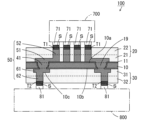
- FIG. 1 is a schematic cross-sectional view showing the configuration of a rewiring board according to one embodiment of the present invention.
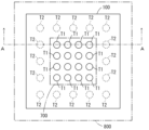
- 2 is a schematic plan view of the rewiring board of FIG. 1.
- FIG. 3 is a schematic bottom view of the rewiring board of FIG. 1.
- FIG. 4 is a partially enlarged plan view of the metal support of FIG. 1.
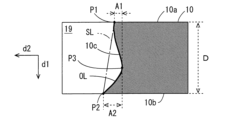
- FIG. 5 is a diagram showing an example of a BB line cross-section of the metal support in FIG.
- FIG. 6 is a diagram showing another example of contour lines of via holes in a metal support.
- FIG. 7 is a diagram showing still another example of contour lines of via holes in the metal support.
- FIG. 8 is a diagram showing still another example of contour lines of via holes in the metal support.
- FIG. 1 is a schematic cross-sectional view showing the configuration of a rewiring board according to one embodiment of the present invention.
- 2 is a schematic plan view of the rewiring board of FIG. 1.
- FIG. 3
- FIG. 9 is a diagram for explaining a preferred shape of the inner peripheral surface of via holes in the metal support.
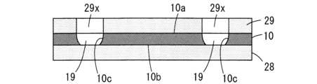
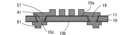
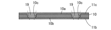
- 10A and 10B are schematic cross-sectional views for explaining an example of a method for manufacturing the rewiring board of FIG. 11A and 11B are schematic cross-sectional views for explaining an example of a method for manufacturing the rewiring board of FIG. 12A and 12B are schematic cross-sectional views for explaining an example of a method for manufacturing the rewiring board of FIG. 13A and 13B are schematic cross-sectional views for explaining an example of a method for manufacturing the rewiring board of FIG. 14A and 14B are schematic cross-sectional views for explaining an example of a method for manufacturing the rewiring board of FIG.
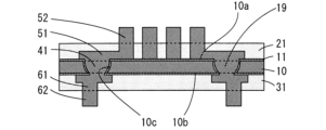
- FIG. 15A and 15B are schematic cross-sectional views for explaining an example of a method for manufacturing the rewiring board of FIG. 16A and 16B are schematic cross-sectional views for explaining an example of a method for manufacturing the rewiring board of FIG. 17A and 17B are schematic cross-sectional views for explaining an example of a method for manufacturing the rewiring board of FIG. 18A and 18B are schematic cross-sectional views for explaining an example of a method for manufacturing the rewiring board of FIG.
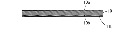
- FIG. 19 is a schematic cross-sectional view for explaining the first method of forming a coating layer on a metal support.
- FIG. 20 is a schematic cross-sectional view for explaining a third method of forming a coating layer on a metal support.
- FIG. 21 is a schematic cross-sectional view for explaining a third method of forming a coating layer on a metal support.
- FIG. 22 is a schematic cross-sectional view for explaining a third method of forming a coating layer on a metal support.
- FIG. 23 is a schematic cross-sectional view for explaining a fourth method of forming a coating layer on a metal support.
- FIG. 24 is a schematic cross-sectional view for explaining a fourth method of forming a coating layer on a metal support.
- FIG. 25 is a schematic cross-sectional view for explaining a fourth method of forming a coating layer on a metal support.
- FIG. 26 is a schematic cross-sectional view for explaining a fourth method of forming a coating layer on a metal support.
- FIG. 27 is a schematic cross-sectional view for explaining a fourth method of forming a coating layer on a metal support.
- FIG. 28 is a schematic cross-sectional view of a rewiring board provided with an
- a wired circuit board and a manufacturing method thereof according to an embodiment of the present invention will be described below with reference to the drawings.
- a rewiring board will be described as an example of the wiring circuit board.
- a rewiring board is arranged between an electronic component such as a semiconductor element and another wiring circuit board such as a rigid printed wiring circuit board (hereinafter abbreviated as a rigid board), and is used to connect fine patterns of the electronic component and other components. It plays a role of converting the pitch from the rough pattern of the wiring circuit board.
- a rewiring board is also called an interposer board.
- FIG. 1 is a schematic cross-sectional view showing the configuration of a rewiring board according to an embodiment of the present invention.
- FIG. 2 is a schematic plan view of the rewiring board 100 of FIG.
- FIG. 3 is a schematic bottom view of the rewiring board 100 of FIG.
- FIG. 1 represents a cross section taken along line AA of FIGS. 2 and 3.
- FIG. 1 the rewiring board 100 is mainly composed of a metal support 10, insulating layers 20 and 30, and a conductor layer 50, and has a thickness of 60 ⁇ m or more and 500 ⁇ m or less. Also, the rewiring board 100 is arranged between the semiconductor element 700 and the rigid board 800 .
- the semiconductor element 700 has a plurality of electrode pads 71 and the rigid substrate 800 has a plurality of electrode pads 81 .
- the semiconductor element 700 is indicated by a one-dot chain line
- the rigid substrate 800 is indicated by a two-dot chain line.
- the metal support 10 is, for example, a metal or alloy containing one or more elements selected from the group consisting of copper, aluminum, iron, nickel, chromium, titanium and molybdenum.
- the metal support 10 is made of stainless steel and formed into a plate shape.
- the surface of the metal support 10 facing the semiconductor element 700 (the surface facing upward in FIG. 1) is referred to as the upper surface 10a
- the surface of the metal support 10 facing the rigid substrate 800 (the surface facing downward in FIG. 1) is referred to as the lower surface. 10b.
- the upper surface 10a and the lower surface 10b according to the present embodiment are parallel to each other, perpendicular to the thickness direction of the metal support 10, and flat.
- the direction in which the upper surface 10a of the metal support 10 faces is the upper side of the rewiring board 100
- the direction in which the lower surface 10b of the metal support 10 faces is the lower side of the rewiring board 100.
- the metal support 10 is not limited to the above examples, and 42 alloy, Invar alloy, or the like may be used.
- an Invar alloy is used for the metal support 10
- the coefficient of linear expansion of the metal support 10 can be adjusted according to changes in the composition of nickel (Ni) in the Invar alloy. In this case, it is possible to suppress the occurrence of warpage in each layer constituting the rewiring board 100 .
- the metal support 10 preferably has a thermal conductivity higher than that of the insulating layers 20 and 30. For example, it has a thermal conductivity of 10 W/mK or more and 400 W/mK or less. . Moreover, the metal support 10 preferably has a thickness of 10 ⁇ m or more and 100 ⁇ m or less, more preferably 15 ⁇ m or more and 60 ⁇ m or less, and further preferably 15 ⁇ m or more and 30 ⁇ m or less. Furthermore, the linear expansion coefficient of the metal support 10 at 25° C. to 200° C. is 0 ⁇ m/K or more and 25 ⁇ m/K or less.
- a coating layer 11 is formed on the outer surface of the metal support 10 . More specifically, in metal support 10 , coating layer 11 is formed so as to entirely cover upper surface 10 a , lower surface 10 b and inner peripheral surface 10 c of each via hole 19 .
- the covering layer 11 is made of, for example, photosensitive polyimide and has a thickness of 1 ⁇ m or more and 15 ⁇ m or less. Note that the coating layer 11 may be formed of other resin such as acrylic resin, polyethernitrile resin, polyethersulfone resin, epoxy resin, polyethylene terephthalate resin, polyethylene naphthalate resin, or polyvinyl chloride resin.
- an inorganic insulating material or an organic insulating material can be used instead of the above resin.
- silicon carbide, silicon dioxide, aluminum nitride, aluminum oxide, or the like can be used as the material of the coating layer 11 .
- the coating layer 11 is formed using a deposition technique such as sputtering or chemical vapor deposition, as described later. be able to.
- the thickness of the coating layer 11 is the same as the thickness (1 ⁇ m or more and 10 ⁇ m or less) when using photosensitive polyimide. can be made even smaller.
- a first insulating layer 21 and a second insulating layer 22 having a predetermined pattern are laminated in this order on the upper surface 10a of the metal support 10 .
- An insulating layer 20 is formed by a first insulating layer 21 and a second insulating layer 22 .
- a third insulating layer 31 and a fourth insulating layer 32 having a predetermined pattern are laminated in this order on the lower surface 10b of the metal support 10.
- An insulating layer 30 is formed by a third insulating layer 31 and a fourth insulating layer 32 .
- the insulating layers 20 and 30 are made of, for example, photosensitive polyimide.
- the insulating layers 20 and 30 may be made of other resin such as acrylic resin, polyethernitrile resin, polyethersulfone resin, epoxy resin, polyethylene terephthalate resin, polyethylene naphthalate resin, or polyvinyl chloride resin.
- a via conductor 41 is provided in each via hole 19 of the metal support 10 with the coating layer 11 interposed therebetween.
- a first conductor layer 51 is formed on the upper surface 10 a of the metal support 10 in addition to the first insulating layer 21 . Specifically, on the upper surface 10 a of the metal support 10 , the first insulating layer 21 non-formation region (region having a pattern opposite to the pattern of the first insulating layer 21 ) is coated with the coating layer 11 interposed therebetween.
- a first conductor layer 51 is formed. A portion of first conductor layer 51 is electrically connected to via conductor 41 .
- a second insulating layer 22 non-formation region (a region having a pattern opposite to the pattern of the second insulating layer 22) is provided with a second A conductor layer 52 is formed.
- a portion of the second conductor layer 52 is electrically connected to the first conductor layer 51 .
- the second conductor layer 52 is formed with a plurality of terminal portions T1 exposed upward in regions where the second insulating layer 22 is not formed.
- a plurality of electrode pads 71 of the semiconductor element 700 are connected via solder S to these terminal portions T1. Therefore, the number and arrangement of the plurality of terminal portions T1 are determined so as to correspond to the number and arrangement of the plurality of electrode pads 71 of the semiconductor element 700.
- a third conductor layer 61 is formed in addition to the third insulating layer 31.
- the third insulating layer 31 non-formation region region having a pattern opposite to the pattern of the third insulating layer 31
- a third conductor layer 61 is formed on the lower surface 10 b of the metal support 10 .
- Part of third conductor layer 61 is electrically connected to via conductor 41 .
- a fourth insulating layer 32 non-formation region is provided with a fourth A conductor layer 62 is formed on the third insulating layer 31 and the third conductor layer 61.
- a portion of the fourth conductor layer 62 is electrically connected to the third conductor layer 61 .
- the fourth conductor layer 62 is formed with a plurality of terminal portions T2 exposed downward in regions where the fourth insulating layer 32 is not formed.
- a plurality of electrode pads 81 of the rigid substrate 800 are connected via solder S to these terminal portions T2. Therefore, the number and arrangement of the plurality of terminal portions T2 are determined so as to correspond to the number and arrangement of the plurality of electrode pads 81 of the rigid substrate 800.
- the conductor layer 50 is formed by the via conductors 41 , the first conductor layer 51 , the second conductor layer 52 , the third conductor layer 61 and the fourth conductor layer 62 .
- the conductor layer 50 is made of copper.
- Conductor layer 50 may be formed of a metal or alloy containing one or more of copper, gold, silver, platinum, lead, tin, nickel, cobalt, indium, rhodium, chromium, tungsten, ruthenium, and the like. good.
- each of the plurality of terminal portions T1 and T2 has a laminated structure of a nickel film and a gold plating film.
- each terminal portion T1 has a structure in which a nickel film and a gold plating film are formed in this order on the surface of the upper end portion of the second conductor layer 52 .
- Each terminal portion T2 has a structure in which a nickel film and a gold plating film are formed in this order on the surface of the lower end portion of the fourth conductor layer 62 .
- each of the terminal portions T1 and T2 may be composed only of a gold-plated film without the nickel film.
- each of the plurality of terminal portions T1 formed on the upper surface of the rewiring board 100 is connected to one of the plurality of terminal portions T2 formed on the lower surface of the rewiring board 100 through the conductor layer 50. electrically connected.
- a plurality of electrode pads 71 of the semiconductor element 700 are connected to the plurality of terminal portions T1 of the rewiring substrate 100, and a plurality of electrode pads 81 of the rigid substrate 800 are connected to the plurality of terminal portions T2 of the rewiring substrate 100. be done. Thereby, the plurality of electrode pads 71 of the semiconductor element 700 and the plurality of electrode pads 81 of the rigid substrate 800 are electrically connected through the rewiring substrate 100 .
- the number of terminal portions T1 located on the top surface of the rewiring board 100 and the number of terminal portions T2 located on the bottom surface of the rewiring board 100 are different. , but the invention is not limited to this. The number of terminal portions T1 located on the top surface of the rewiring board 100 and the number of terminal portions T2 located on the bottom surface of the rewiring board 100 do not have to match.
- the conductor layer 50 and the metal support 10 are made of metal. Therefore, the conductor layer 50 and the metal support 10 basically have a higher thermal conductivity than the resin forming the insulating layers 20, 30 and the like. Moreover, the metal support 10 is formed so as to extend over the entire rewiring board 100 in plan view. Therefore, if the heat generated in the semiconductor element 700 can be efficiently transferred to the metal support 10, the heat radiation efficiency of the semiconductor element 700 will be improved.
- part of the heat generated from the semiconductor element 700 is transferred to the conductor layer 50 through the plurality of terminal portions T1. Therefore, in order to efficiently transfer the heat transferred to the conductor layer 50 to the metal support 10, the area of the conductor layer 50 formed on the outer surface of the metal support 10 via the coating layer 11 is enlarged. is preferred.
- FIG. 4 is a partially enlarged plan view of the metal support 10 of FIG.
- FIG. 5 is a diagram showing an example of a BB line cross section of the metal support 10 of FIG.
- the cross section of FIG. 5 is parallel to the thickness direction of the metal support 10 and passes through the opening of one via hole 19 .
- the thickness direction of the metal support 10 shown in FIG. 5 and FIGS. 6 to 9, which will be described later is referred to as a first direction d1.
- the direction orthogonal to the first direction d1 in the cross section of the metal support 10 shown in FIG. 5 and FIGS. 6 to 9, which will be described later, is called a second direction d2.
- first direction d1 is a direction parallel to the thickness direction of the metal support 10 and directed from the upper surface 10a to the lower surface 10b.
- the second direction d2 is a direction orthogonal to the thickness direction of the metal support 10 and directed from the outside of the via hole 19 to the inside of the via hole 19 .
- the area of the opening at the lower end of the via hole 19 is smaller than the area of the opening at the upper end of the via hole 19 . Therefore, the inner peripheral surface 10c of the via hole 19 is inclined from the upper surface 10a to the lower surface 10b of the metal support 10 in the first direction d1 and the second direction d2.
- the contour line OL representing a part of the inner peripheral surface 10c of the via hole 19 is curved so as to be gently depressed.
- the outline OL is macroscopically shown to such an extent that unevenness of about 0.1 ⁇ m cannot be discerned.
- the fact that the contour line OL is curved includes the fact that a part of the contour line OL is bent like a polygonal line.
- a first point P1, a second point P2 and a third point P3 are defined on the contour line OL.
- the first point P1 is located on the upper surface 10a of the metal support 10 at one end of the contour line OL.
- the second point P2 is located on the bottom surface 10b of the metal support 10 at the other end of the contour line OL.
- the third point P3 is located at the farthest portion of the contour line OL from the straight line SL connecting the first point P1 and the second point P2. Also, the third point P3 is located between the first point P1 and the second point P2 in the second direction d2.
- the via hole 19 of the metal support 10 is defined so that "A1" is the distance between the first point P1 and the third point P3 in the second direction d2, and "A2" is the distance in the second direction d2.
- the contour line OL is formed so as to satisfy the following formula (1).
- the contour line OL is curved.
- the area of the inner peripheral surface 10c of the via hole 19 is larger than when the contour line OL is formed in a straight line.
- the contour line OL satisfies the above formula (1)
- the area of the inner peripheral surface 10c can be sufficiently increased compared to when the contour line OL does not satisfy the above formula (1).
- at least part of the inner peripheral surface 10c is inclined with respect to the first direction d1.
- the coating layer 11 is formed on the inner peripheral surface 10c by sputtering, if the contour line OL satisfies the relationship of the above formula (1), at least a part of the inner peripheral surface 10c is obliquely upward or obliquely downward. turn to This makes it easier to form the covering layer 11 than when the contour line OL is parallel to the first direction d1. Thereby, the reliability of the coating layer 11 covering the inner peripheral surface 10c is improved.
- the via hole 19 of the metal support 10 is preferably formed so that the contour line OL satisfies the following formula (2).
- the via hole 19 of the metal support 10 is more preferably formed so that the contour line OL satisfies the following formula (3).
- the contour line OL preferably further satisfies the following formula (4).
- the contour line OL is curved so as to be gently depressed.
- the via hole 19 of the metal support 10 may be formed so that the contour line OL has the following shape.
- FIG. 6 is a diagram showing another example of the contour line OL of the via hole 19 in the metal support 10.
- FIG. FIG. 6 shows a cross section showing part of the metal support 10 .
- the cross section corresponds to the cross section of FIG. 5 and is a cross section parallel to the thickness direction of the metal support 10 and passing through the opening of the via hole 19 .
- the contour line OL is curved with a relatively large depression. Therefore, the third point P3 is not positioned between the first point P1 and the second point P2 in the second direction d2. Even in such a case, if the contour line OL satisfies the above formula (1), it is possible to obtain the same effect as in the example of FIG.
- FIG. 7 is a diagram showing still another example of the contour line OL of the via hole 19 in the metal support 10.
- FIG. FIG. 7 shows a cross section showing part of the metal support 10 .
- the cross section corresponds to the cross section of FIG. 5 and is a cross section parallel to the thickness direction of the metal support 10 and passing through the opening of the via hole 19 .
- the contour line OL is curved so as to gently swell toward the inside of the via hole 19 .
- the third point P3 is located between the first point P1 and the second point P2 in the second direction d2. Even in such a case, if the contour line OL satisfies the above formula (1), it is possible to obtain the same effect as in the example of FIG.
- FIG. 8 is a diagram showing still another example of the contour line OL of the via hole 19 in the metal support 10.
- FIG. FIG. 8 shows a cross section showing part of the metal support 10 .
- the cross section corresponds to the cross section of FIG. 5 and is a cross section parallel to the thickness direction of the metal support 10 and passing through the opening of the via hole 19 .
- the contour line OL is curved so as to swell relatively large toward the inside of the via hole 19 .
- the third point P3 is not located between the first point P1 and the second point P2 in the second direction d2. Even in such a case, if the contour line OL satisfies the above formula (1), it is possible to obtain the same effect as in the example of FIG.
- FIG. 9 is a diagram for explaining a preferred shape of the inner peripheral surface 10c of the via hole 19 in the metal support 10.
- FIG. 9 four cross-sectional views of the metal support 10 are shown aligned from top to bottom.
- a plurality of cross-sectional views in FIG. 9 are partially enlarged cross-sectional views of the metal support 10 enlarging a common portion of the contour line OL in FIG.
- the contour line OL is shown microscopically to the extent that irregularities of about 0.1 ⁇ m can be identified.
- a plurality of virtual points arranged at substantially regular intervals on the contour line OL are set.
- the two virtual points A bending point CP is set at a position between (for example, an intermediate position). That is, in the contour line OL, the inflection point CP is set at a portion where the inclination changes greatly or a portion in the vicinity thereof.
- the height h of each triangle is calculated.
- the height of each triangle is calculated using a straight line connecting two of the three bending points CP that are not located in the center as the base.
- the largest height h among the heights h of the plurality of triangles calculated in this way is set as the maximum height of the unevenness of the contour line OL.
- the inner peripheral surface 10c of the via hole 19 is preferably formed so that the maximum height of the unevenness of the contour line OL is 0.6 ⁇ m or more.
- the surface area of the inner peripheral surface 10c of the via hole 19 can be made sufficiently large by microscopically having relatively large irregularities on the inner peripheral surface 10c of the via hole 19 .
- the amount of heat transferred from inner peripheral surface 10c of via hole 19 to metal support 10 per unit time can be increased.
- the inner peripheral surface 10c of the via hole 19 is formed so that the maximum height of the unevenness of the contour line OL is 0.9 ⁇ m or more. Further, it is more preferable that the inner peripheral surface 10c of the via hole 19 is formed so that the maximum height of the unevenness of the contour line OL is 1.0 ⁇ m or more.
- a plurality of inflection points CP are set on the contour line OL by setting a plurality of virtual points on the contour line OL.
- a plurality of inflection points CP on the contour line OL are determined, for example, by defining a virtual straight line parallel to the first direction d1 and passing through substantially the center of the via hole 19, and then determining the distance of each part of the contour line OL with respect to the virtual straight line. may be defined.
- the contour line OL includes a first inclined portion that inclines toward the virtual line in the first direction d1 and a second inclined portion that inclines away from the virtual line in the first direction d1. If there are two sloped portions, the inflection point CP may be set between the first and second sloped portions (for example, the boundary portion).
- FIGS. 10 to 18 are schematic cross-sectional views for explaining an example of a method for manufacturing the rewiring board 100 of FIG.
- the schematic cross-sectional views shown in FIGS. 10 to 18 correspond to the schematic cross-sectional view of FIG.
- the rewiring board 100 is manufactured by a roll-to-roll method.
- a roll around which a long metal support 10 made of stainless steel is wound (hereinafter referred to as a delivery roll) is prepared.
- a metal support 10 is fed out from a prepared feeding roll.
- the metal support 10 delivered from the delivery roll is wound around another roll.
- FIG. 10 shows a cross section of part of the metal support 10 unwound from the unwind roll. According to the roll-to-roll method, each area of the metal support 10 is sequentially subjected to the following treatments while the long metal support 10 moves in the longitudinal direction.
- a photosensitive dry film resist is laminated on the upper surface 10a of the metal support 10 to form a resist film.
- a resist film formed on the upper surface 10a of the metal support 10 is exposed in a predetermined pattern and developed.
- a photosensitive dry film resist is laminated on the lower surface 10b of the metal support 10 to form a resist film.
- a resist film formed on the lower surface 10b of the metal support 10 is exposed and developed.
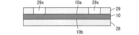
- an etching resist 29 having a plurality of openings 29x is formed on the upper surface 10a of the metal support 10
- an etching resist 28 is formed on the lower surface 10b of the metal support 10, as shown in FIG.
- the plurality of openings 29x of this example are formed so as to overlap with the plurality of regions of the metal support 10 where the plurality of via holes 19 will be formed in a later step.
- a plurality of portions of the metal support 10 exposed through the plurality of openings 29x of the etching resist 29 are etched.
- a plurality of via holes 19 are thereby formed in the metal support 10 .
- the metal support 10 is etched from the top surface 10a of the metal support 10 toward the bottom surface 10b.
- the inner peripheral surfaces 10c of the plurality of via holes 19 are formed so as to be gently recessed from the upper surface 10a to the lower surface 10b.
- Each via hole 19 may be formed by etching from the bottom surface 10b of the metal support 10 to the top surface 10a in addition to etching from the top surface 10a to the bottom surface 10b of the metal support 10 .
- the inner peripheral surface 10c of the via hole 19 may have a locally reduced diameter at the central portion in the thickness direction of the metal support 10 .
- the inner peripheral surface 10c of the via hole 19 may be formed so as to protrude inwardly of the via hole 19 (see FIG. 8).
- the via hole 19 may be formed by, for example, laser processing instead of etching. In this case, the via hole 19 must be formed so that the contour line OL indicating the cross section of the inner peripheral surface 10c satisfies the relationship of formula (1) above.
- the minimum value of the inner diameter of each via hole 19 is, for example, preferably 10 ⁇ m or more and 100 ⁇ m or less, more preferably 15 ⁇ m or more and 80 ⁇ m or less. More preferably, the thickness is 20 ⁇ m or more and 60 ⁇ m or less.
- the etching resists 29 and 28 are removed from the upper surface 10a and the lower surface 10b of the metal support 10. Then, as shown in FIG. Thereafter, as shown in FIG. 14, a coating layer 11 made of photosensitive polyimide is formed on the exposed upper and lower surfaces 10a and 10b of the metal support 10 and the inner peripheral surfaces 10c of the via holes 19. As shown in FIG. Covering layer 11 can be formed in several ways. A specific example of the method for forming the coating layer 11 will be described later.
- the minimum value of the inner diameter of the portion of the coating layer 11 covering the inner peripheral surface 10c is 10 ⁇ m or more and 100 ⁇ m or less. , more preferably 15 ⁇ m or more and 80 ⁇ m or less, and even more preferably 20 ⁇ m or more and 60 ⁇ m or less.
- via conductors 41 made of copper are formed in the respective via holes 19 of the metal support 10 (via filling).
- a first conductor layer 51 made of copper is formed in a predetermined region on the upper surface 10 a of the metal support 10 .
- a third conductor layer 61 made of copper is formed in a predetermined region on the lower surface 10b of the metal support 10.
- the via filling and the formation of the first conductor layer 51 and the third conductor layer 61 may be performed simultaneously or separately. Specifically, the formation of the conductors (41, 51, 61) described above is performed, for example, as follows.
- a seed layer made of, for example, a chromium thin film and a copper thin film is formed on the surface of the coating layer 11 covering the upper surface 10a, the lower surface 10b and the inner peripheral surface 10c of the metal support 10 by sputtering or electroless plating.
- a plating resist having a predetermined pattern is formed on the seed layer.
- the above conductors (41, 51, 61) are partially formed by electroplating on the seed layer exposed through the openings of the plating resist. The portions of the first conductor layer 51 and the third conductor layer 61 formed here are used as wiring portions.
- the first conductor layer 51 and the third conductor layer 61 include via portions in addition to the wiring portions described above. Therefore, after forming the wiring portions of the first conductor layer 51 and the third conductor layer 61, the via portions of the first conductor layer 51 and the third conductor layer 61 are further formed by electroplating using a plating resist. be done.
- the plating resist is peeled off, and the exposed portion of the seed layer (the portion where the conductor is not formed) is removed by etching. Furthermore, a barrier layer is formed on the outer surfaces of the conductors (41, 51, 61) to suppress the diffusion of copper from the conductors (41, 51, 61).
- the barrier layer is made of, for example, a nickel thin film. Note that the barrier layer may not be formed. In FIG. 15, illustration of the seed layer and the barrier layer is omitted.
- a first insulating layer made of photosensitive polyimide is applied to areas of the upper surface 10a of the metal support 10 where the first conductor layer 51 is not formed.
- a layer 21 is formed.
- the first insulating layer 21 is also formed in the region of the wiring portion of the first conductor layer 51 .
- the wiring portion of the first conductor layer 51 is covered with the first insulating layer 21, and the via portion (portion other than the wiring portion) of the first conductor layer 51 is exposed.
- a third insulating layer 31 made of photosensitive polyimide is formed in a region of the lower surface 10b of the metal support 10 where the third conductor layer 61 is not formed.
- the third insulating layer 31 is also formed in the region of the wiring portion of the third conductor layer 61 .
- the wiring portion of the third conductor layer 61 is covered with the third insulating layer 31, and the via portion (portion other than the wiring portion) of the third conductor layer 61 is exposed.
- the first insulating layer 21 and the third insulating layer 31 are formed by applying a photosensitive polyimide precursor to the upper surface 10a and the lower surface 10b of the metal support 10, and exposing and developing the precursor. . Further, the formed first insulating layer 21 and third insulating layer 31 are cured.
- the barrier layer existing in a predetermined region on the upper surface of the first conductor layer 51 is removed. Also, the barrier layer existing in a predetermined region on the lower surface of the third conductor layer 61 is removed.
- a second conductor layer 52 is formed in a predetermined region on the upper surface of the first conductor layer 51 and the upper surface of the first insulating layer 21 from which the barrier layer has been removed.
- a fourth conductor layer 62 is formed in a predetermined region on the lower surface of the third conductor layer 61 and the lower surface of the third insulating layer 31 from which the barrier layer has been removed.
- Each of the second conductor layer 52 and the fourth conductor layer 62 has a wiring portion and a via portion similarly to the first conductor layer 51 and the third conductor layer 61 . Therefore, the formation of the second conductor layer 52 and the fourth conductor layer 62 is basically performed in the same procedure as the formation of the first conductor layer 51 and the third conductor layer 61 .
- a second insulating layer made of photosensitive polyimide is formed on the upper surfaces of the first insulating layer 21 and the first conductive layer 51 where the second conductive layer 52 is not formed. 22 are formed.
- the second insulating layer 22 is also formed in the region of the wiring portion of the second conductor layer 52 .
- the wiring portion of the second conductor layer 52 is covered with the second insulating layer 22, and the via portion (portion other than the wiring portion) of the second conductor layer 52 is exposed.
- the fourth insulating layer 32 made of photosensitive polyimide is formed on the lower surfaces of the third insulating layer 31 and the third conductive layer 61 in areas where the fourth conductive layer 62 is not formed.
- the fourth insulating layer 32 is also formed in the region of the wiring portion of the fourth conductor layer 62 .
- the wiring portion of the fourth conductor layer 62 is covered with the fourth insulating layer 32, and the via portion (portion other than the wiring portion) of the fourth conductor layer 62 is exposed.
- the second insulating layer 22 and the fourth insulating layer 32 are basically formed in the same procedure as the first insulating layer 21 and the third insulating layer 31 are formed.
- the barrier layer formed on the plurality of portions exposed upward of the second conductor layer 52 is removed, and the terminal portions T1 are formed on the plurality of portions of the second conductor layer 52 from which the barrier layer has been removed. (FIG. 1) is formed.
- the barrier layer formed on the plurality of portions exposed downward of the fourth conductor layer 62 is removed, and the terminal portions T2 ( 1) is formed.
- the terminal portions T1 and T2 are formed by gold plating, for example.
- FIG. 19 is a schematic cross-sectional view for explaining a first method of forming coating layer 11 on metal support 10. As shown in FIG. In the first forming method, photosensitive polyimide is used as the material of the coating layer 11 .
- a photosensitive polyimide precursor is applied to cover the upper surface 10a and the lower surface 10b.
- each via hole 19 of the metal support 10 is filled with a photosensitive polyimide precursor so as to fill the internal space of the inner peripheral surface 10c of each via hole 19 .
- the coated and filled photosensitive polyimide precursor is then exposed and developed.
- temporary covering layer 11a is formed so as to cover upper surface 10a and lower surface 10b of metal support 10 and to fill the internal spaces of a plurality of via holes 19 .
- the formed temporary covering layer 11a is cured.
- through-holes are formed in portions of the temporary covering layer 11a formed in each via hole 19 by laser processing or etching, for example.
- the space above and below the metal support 10 communicate with each other through the internal spaces of the via holes 19 of the metal support 10, and the coating layer 11 is formed on the outer surface of the metal support 10 ( See Figure 14).
- a through hole passing through the inside of the via hole 19 may be formed by using a photosensitive polyimide exposure technique. For example, it may be formed by irradiating or not irradiating the portion of the temporary covering layer 11a in the via hole 19 with the exposure light when forming the temporary covering layer 11a.
- the surface state of the inner peripheral surface 10c of the via hole 19 does not affect the surface condition. It is possible to form a coating layer 11 with high reliability without any defects.
- a precursor of liquid photosensitive polyimide is used to form the coating layer 11 on the metal support 10, but the elements to be used for forming the coating layer 11 are Not limited.
- a photosensitive polyimide film formed in a sheet shape, a sheet-like A film containing a photosensitive material other than photosensitive polyimide that is formed into a sheet or a film containing a non-photosensitive material that is formed into a sheet may be used.
- films containing photosensitive materials other than photosensitive polyimide include polymeric materials such as acrylic resins, epoxy resins, and phenol resins.
- Materials for films containing photosensitive materials other than photosensitive polyimide include materials in which reinforcing agents such as fillers are dispersed in the above polymer materials.
- the first conductor layer 11 When forming the first conductor layer 11 from a film, one film is attached to the upper surface 10a of the metal support 10 and the other film is attached to the lower surface 10b of the metal support 10. As a result, the upper surface 10a and the lower surface 10b of the metal support 10 are covered with the two films, respectively, and the internal space of the inner peripheral surface 10c of each via hole 19 of the metal support 10 is filled with the material constituting the film. be.
- a through hole is formed in the portion of the temporary covering layer 11a formed in each via hole 19 using an exposure technique. be done. If the material of the film used to form the covering layer 11 contains a reinforcing agent or is a non-photosensitive material, the portion of the temporary covering layer 11a formed in each via hole 19 may be subjected to, for example, laser processing or A through-hole is formed by processing (drilling) using a drill.
- the type of coating layer 11 formed on the metal support 10 does not have to be one type.
- the covering layer 11 may be composed of a plurality of elements made of a plurality of types of materials.
- Second method of forming coating layer 11 on metal support 10 As a specific example of the coating layer 11 on the metal support 10, a second method of forming will be described. Also in the second formation method, photosensitive polyimide is used as the material of the coating layer 11 as in the first formation method.
- the coated photosensitive polyimide precursor is exposed and developed. Thereby, a coating layer 11 is formed on the outer surface of the metal support 10 (see FIG. 14).
- the coating layer 11 having a thickness of 5 ⁇ m or more and 15 ⁇ m or less can be formed on the outer surface of the metal support 10 .
- an insulating layer such as the temporary covering layer 11a is provided inside the via hole 19 as in the first forming method. No layers need to be embedded. Therefore, the time required for forming the covering layer 11 is reduced.
- the third method of forming the coating layer 11 first, one surface (the lower surface 10b in this example) of the metal support 10 on which the plurality of via holes 19 are not formed is covered with the lower surface 10b of the metal support 10.
- a photosensitive polyimide precursor is applied as follows. Thereby, as shown in FIG. 20, the first temporary covering layer 11b is formed so as to cover the lower surface 10b of the metal support 10. Then, as shown in FIG. Preferably, the formed first temporary covering layer 11b is cured.
- a plurality of via holes 19 are formed in the metal support 10 according to the examples of FIGS.
- through holes are not formed in portions of the first temporary covering layer 11 b overlapping the via holes 19 in the thickness direction of the metal support 10 .
- the internal spaces of the plurality of via holes 19 are not open to the space below the metal support 10 due to the first temporary covering layer 11b.
- a lower end of each via hole 19 is blocked by a portion of the first temporary covering layer 11b.
- a photosensitive polyimide precursor is applied so as to cover the other surface (the upper surface 10a in this example) of the metal support 10 in FIG.
- each via hole 19 of the metal support 10 is filled with a photosensitive polyimide precursor so as to fill the internal space of the inner peripheral surface 10c of each via hole 19 .
- the second temporary covering layer 11c is formed so as to cover the upper surface 10a of the metal support 10 and fill the internal spaces of the plurality of via holes 19.
- the formed second temporary covering layer 11c is cured.
- the portion of the first temporary covering layer 11b covering the lower end of each via hole 19 and the portion of the second temporary covering layer 11c formed in each via hole 19 are irradiated with, for example, a laser beam.
- a through hole is formed by processing or etching.
- the space above and below the metal support 10 communicate with each other through the internal spaces of the via holes 19 of the metal support 10, and the coating layer 11 is formed on the outer surface of the metal support 10 ( See Figure 14).
- the through hole passing through the inside of the via hole 19 may be formed by laser processing or etching, or may be formed by using a photosensitive polyimide exposure technique. .
- the third method of forming the coating layer 11 there is no through-hole in the metal support 10 when the first temporary coating layer 11b is formed on the metal support 10. Therefore, for example, when the photosensitive polyimide precursor is applied to the lower surface 10 b of the metal support 10 , the precursor is less likely to flow onto the upper surface 10 a of the metal support 10 . Further, when the second temporary covering layer 11c is formed on the metal support 10, the first temporary covering layer 11b does not have through-holes. Therefore, for example, when the photosensitive polyimide precursor is applied onto the upper surface 10 a of the metal support 10 , the precursor is less likely to flow onto the lower surface 10 b of the metal support 10 . As a result, it is easy to form the first temporary covering layer 11b and the second temporary covering layer 11c.
- the second temporary covering layer 11c is embedded in each via hole 19 during the process of forming the covering layer 11, so that the surface condition of the inner peripheral surface 10c of the via hole 19 is improved.
- a highly reliable coating layer 11 can be formed without being affected by
- the coating layer 11 for the metal support 10 As a specific example of the coating layer 11 for the metal support 10, a fourth formation method will be described.
- the coating layer 11 may be formed on the metal support 10 (the metal support 10 having the via holes 19 formed therein) of FIG. 13 as follows.
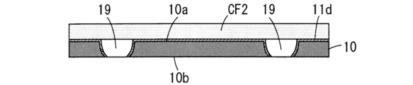
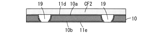
- 23 to 27 are schematic cross-sectional views for explaining a fourth method of forming the coating layer 11 on the metal support 10.
- a carrier film CF1 is attached to the lower surface 10b of the metal support 10 of FIG. 13 in which a plurality of via holes 19 are formed.
- the carrier film CF1 for example, a polyimide film with an adhesive is used.
- a coating layer 11 d is formed on the upper surface 10 a of the metal support 10 and the inner peripheral surfaces 10 c of the plurality of via holes 19 from above the metal support 10 .
- the coating layer 11d is formed by applying a photosensitive polyimide precursor onto the upper surface 10a and the inner peripheral surface 10c of the metal support 10, and exposing and developing the applied photosensitive polyimide precursor. .
- the formed covering layer 11d is cured.
- the carrier film CF1 is peeled off from the bottom surface 10b of the metal support 10.
- a carrier film CF2 is laminated onto the upper surface 10a of the metal support 10 with the coating layer 11d interposed therebetween.
- the carrier film CF2 for example, a polyimide film with an adhesive is used similarly to the carrier film CF1.
- a coating layer 11e is formed on the lower surface 10b of the metal support 10 from below the metal support 10.
- Formation of the covering layer 11e is basically performed in the same procedure as that of the covering layer 11d.
- the carrier film CF2 is peeled off from the covering layer 11e.
- Silicon carbide, silicon dioxide, aluminum nitride, or the like can also be used as the material for coating layer 11 according to the present embodiment.
- the covering layer 11 is formed by sputtering, for example.
- silicon carbide or aluminum oxide is used as the material of the coating layer 11
- the coating layer 11 is formed by chemical vapor deposition, for example. Therefore, in the first to fourth forming methods described above, the coating layer 11 may be formed by sputtering, chemical vapor deposition, or the like, depending on the material or the like that constitutes the coating layer 11 .
- the first insulating layer 21 and the third insulating layer 31 are formed on the upper surface 10a and the lower surface 10b of the metal support 10 with the covering layer 11 interposed therebetween.
- Via conductors 41 are formed in the via holes 19 of the metal support 10 with the coating layer 11 interposed therebetween.
- the contour line OL of the inner peripheral surface 10c in the cross section of the via hole 19 is curved.
- the area of the inner peripheral surface 10c of the via hole 19 is larger than when the contour line OL is formed in a straight line.
- the area of the inner peripheral surface 10c of the via hole 19 is larger than when the contour line OL does not satisfy the above formula (1).
- the contour line OL satisfies the relationship of formula (1) above, at least a portion of the inner peripheral surface 10c of each via hole 19 faces a direction that is inclined with respect to the first direction d1. Therefore, the formation of the coating layer 11 on the inner peripheral surface 10c of the via hole 19 becomes easier than when the contour line OL is parallel to the first direction d1. Thereby, the reliability of the coating layer 11 covering the inner peripheral surface 10c of the via hole 19 is improved. Therefore, insulation between the metal support 10 and the conductor layer 50 is ensured.
- the metal support 10 preferably has a thickness of 10 ⁇ m or more and 100 ⁇ m or less.
- the heat received by the metal support 10 from the semiconductor element 700 can be efficiently transferred to the rigid substrate 800 connected to the rewiring board 100 as compared with the case where the thickness of the metal support is greater than 100 ⁇ m. can.
- the amount of heat transferred between the semiconductor device 700 and the metal support 10 is prevented from being limited due to insufficient heat capacity of the metal support 10 .
- the metal support 10 has a thermal conductivity of, for example, 10 W/mK or higher.
- the amount of heat transferred from the inner peripheral surface 10c of each via hole 19 to the metal support 10 per unit time is increased compared to when the thermal conductivity of the metal support 10 is less than 10 W/mK. be able to.
- the linear expansion coefficient of the metal support 10 at 25°C to 200°C is 0 ⁇ m/K or more and 25 ⁇ m/K or less. In this case, it is possible to prevent the metal support 10 from greatly deforming due to a change in the temperature of the rewiring board 100 . Thereby, the reliability of the rewiring board 100 is improved.
- each via hole 19 is formed by etching a predetermined portion of the metal support 10, for example.
- the inner peripheral surface 10c of the via hole 19 is inclined with respect to the first direction d1.
- the surface condition of the inner peripheral surface 10c of the via hole 19 becomes rough. As a result, it becomes possible to secure a wider surface area on the inner peripheral surface 10c of the via hole 19 without requiring complicated processing.
- the metal support 10 preferably contains a component that improves adhesion between the metal support 10 and the coating layer 11 .
- a component that improves adhesion between the metal support 10 and the coating layer 11 In this case, peeling of the coating layer 11 from the surface of the metal support 10 is suppressed. As a result, the insulation between the metal support 10 and the conductor layer 50 is ensured, so the reliability of the rewiring board 100 is improved.
- Components that improve adhesion between the metal support 10 and the coating layer 11 include copper, aluminum, nickel, chromium, titanium, molybdenum, and the like.
- a coating layer is formed on the outer surface of the metal support 10 in order to obtain insulation between the metal support 10 and the conductor layer 50. 11 is formed.
- the outer surface of the metal support 10 and the coating layer 11 are provided.
- An adhesion-enhancing layer that improves adhesion with the layer 11 may be formed.
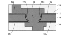
- FIG. 28 is a schematic cross-sectional view of a rewiring board 100 having an adhesion enhancing layer.
- FIG. 28 shows an enlarged cross section of one via hole 19 of the metal support 10 of the rewiring board 100 and its peripheral portion.
- an adhesion-enhancing layer 12 is formed between the upper surface 10a, the lower surface 10b and the inner peripheral surface 10c of the metal support 10 and the covering layer 11.
- FIG. 28 shows an adhesion-enhancing layer 12 between the upper surface 10a, the lower surface 10b and the inner peripheral surface 10c of the metal support 10 and the covering layer 11.
- the adhesion-enhancing layer 12 contains a component that improves adhesion between the metal support 10 and the coating layer 11, and is, for example, sputtered or chemically applied to the upper surface 10a, the lower surface 10b, and the inner peripheral surface 10c of the metal support 10. It is formed by performing a film forming process using a vapor deposition method or the like.
- the adhesion-enhancing layer 12 contains a component that improves the adhesion between the metal support 10 and the coating layer 11, and is anodic to the upper surface 10a, the lower surface 10b and the inner peripheral surface 10c of the metal support 10, for example. It is formed by performing surface treatment such as oxidation treatment.
- the adhesion-enhancing layer 12 improves the adhesion between the metal support 10 and the coating layer 11 , peeling of the coating layer 11 from the metal support 10 is suppressed. As a result, the insulation between the metal support 10 and the conductor layer 50 is ensured, so the reliability of the metal support 10 is improved.
- the content of the chromium or aluminum oxide in the adhesion-strengthening layer 12 is preferably 50% by weight or less.
- Chromium and aluminum have a lower thermal conductivity due to oxidation. According to the above configuration, the decrease in thermal conductivity of the adhesion-strengthening layer 12 is reduced compared to the case where the content of chromium or aluminum oxide in the adhesion-strengthening layer 12 is greater than 50% by weight. Therefore, deterioration in heat dissipation efficiency of the semiconductor element 700 and the rigid substrate 800 due to the adhesion enhancing layer 12 is reduced.
- the coating layer 11 is formed over the entire top surface 10a, bottom surface 10b and inner peripheral surface 10c of the metal support 10 .
- the coating layer 11 includes the inner peripheral surface 10c of the via hole 19 of the metal support 10, the region of the upper surface 10a of the metal support 10 where the first conductor layer 51 is formed, and the metal support 10. may be formed only in the region where the third conductor layer 61 is formed on the lower surface 10b of the .
- the coating layer 11 according to the above embodiment is used on the upper surface 10a of the metal support 10 to ensure insulation between the first conductor layer 51 and the metal support 10.
- the invention is not limited to this.
- the covering layer 11 may be formed on the upper surface 10 a of the metal support 10 such that a portion of the first conductor layer 51 is in direct contact with the upper surface 10 a of the metal support 10 .
- the portion of the first conductor layer 51 that is in direct contact with the upper surface 10a of the metal support 10 is used for efficient heat transfer between the electronic component provided on the upper surface 10a of the metal support 10 and the metal support 10.
- a heat transfer wiring thermal wiring can be used to transfer the heat.
- the coating layer 11 according to the above embodiment is used to ensure insulation between the third conductor layer 61 and the metal support 10 on the lower surface 10b of the metal support 10, but the present invention is used. is not limited to this.
- the covering layer 11 may be formed on the bottom surface 10b of the metal support 10 so that a portion of the third conductor layer 61 is in direct contact with the bottom surface 10b of the metal support 10 .
- the portion of the third conductor layer 61 that is in direct contact with the lower surface 10b of the metal support 10 is used for efficient heat transfer between the electronic component provided on the lower surface 10b of the metal support 10 and the metal support 10.
- a heat transfer wiring thermal wiring can be used to transfer the heat.
- the above embodiment is an example in which the present invention is applied to a rewiring board, but the present invention is not limited to this and may be applied to other wiring circuit boards having via holes. Further, the rewiring board 100 according to the above embodiment may constitute a part of the semiconductor package board.
- the insulating layer 20 is formed of the first insulating layer 21 and the second insulating layer 22, but the present invention is not limited to this. Insulating layer 20 may be a single insulating layer or may be formed by other numbers of insulating layers. Moreover, although the insulating layer 30 is formed of the third insulating layer 31 and the fourth insulating layer 32 in the above embodiment, the present invention is not limited to this. Insulating layer 30 may be a single insulating layer or may be formed by other numbers of insulating layers. In these cases, the shape of the conductor layer 50 is determined according to the configuration of the insulating layers 20 and 30 .
- the contour line OL in the cross section of the inner peripheral surface 10c of the via hole 19 is a curved curve, but the present invention is not limited to this.
- Contour line OL in the cross section of inner peripheral surface 10c of via hole 19 may be a straight line connecting first point P1 and second point P2.
- the semiconductor element 700 and the rigid substrate 800 are examples of the electronic component
- the rewiring board 100 is an example of the wiring circuit board
- the upper surface 10a or the lower surface 10b of the metal support 10 is the first surface.
- the lower surface 10b or the upper surface 10a of the metal support 10 is an example of the second surface
- the via hole 19 is an example of the via hole
- the metal support 10 is an example of the metal support
- the coating layer 11 is an example of the metal support. It is an example of an insulating coating layer.
- the conductor layer 50 is an example of a conductor layer
- the first direction d1 is an example of a first direction
- the first point P1 is an example of a first point
- the second point P2 is an example of a first point. 2 points
- the third point P3 is an example of the third point
- the contour line OL is an example of the contour line
- the second direction d2 is an example of the second direction.
- the plurality of bending points CP are examples of the plurality of bending points
- the adhesion enhancing layer 12 is an example of the adhesion enhancing layer
- the semiconductor element 700 is an example of the first electronic component
- the rigid substrate 800 is an example of the first electronic component.
- the temporary covering layer 11a is an example of the temporary insulating covering layer
- the first temporary covering layer 11b is an example of the first insulating covering layer
- the second temporary covering layer 11c is an example of the second insulating coating layer.
Landscapes
- Engineering & Computer Science (AREA)
- Microelectronics & Electronic Packaging (AREA)
- Manufacturing & Machinery (AREA)
- Insulated Metal Substrates For Printed Circuits (AREA)
- Structure Of Printed Boards (AREA)
- Printing Elements For Providing Electric Connections Between Printed Circuits (AREA)
- Production Of Multi-Layered Print Wiring Board (AREA)
Priority Applications (3)
| Application Number | Priority Date | Filing Date | Title |
|---|---|---|---|
| JP2024501010A JPWO2023157502A1 (https=) | 2022-02-16 | 2022-12-28 | |
| CN202280091909.5A CN118715876A (zh) | 2022-02-16 | 2022-12-28 | 布线电路基板及其制造方法 |
| KR1020247031053A KR20240147692A (ko) | 2022-02-16 | 2022-12-28 | 배선 회로 기판 및 그의 제조 방법 |
Applications Claiming Priority (2)
| Application Number | Priority Date | Filing Date | Title |
|---|---|---|---|
| JP2022022465 | 2022-02-16 | ||
| JP2022-022465 | 2022-02-16 |
Publications (1)
| Publication Number | Publication Date |
|---|---|
| WO2023157502A1 true WO2023157502A1 (ja) | 2023-08-24 |
Family
ID=87578067
Family Applications (1)
| Application Number | Title | Priority Date | Filing Date |
|---|---|---|---|
| PCT/JP2022/048683 Ceased WO2023157502A1 (ja) | 2022-02-16 | 2022-12-28 | 配線回路基板およびその製造方法 |
Country Status (5)
| Country | Link |
|---|---|
| JP (1) | JPWO2023157502A1 (https=) |
| KR (1) | KR20240147692A (https=) |
| CN (1) | CN118715876A (https=) |
| TW (1) | TW202344157A (https=) |
| WO (1) | WO2023157502A1 (https=) |
Citations (9)
| Publication number | Priority date | Publication date | Assignee | Title |
|---|---|---|---|---|
| JPH10135593A (ja) * | 1996-10-31 | 1998-05-22 | Shirai Denshi Kogyo Kk | プリント回路用基板 |
| JP2004179291A (ja) * | 2002-11-26 | 2004-06-24 | Ibiden Co Ltd | 配線板および配線板の製造方法 |
| JP2006100631A (ja) * | 2004-09-30 | 2006-04-13 | Tdk Corp | 配線基板及びその製造方法 |
| JP2008028376A (ja) * | 2006-06-20 | 2008-02-07 | Sanyo Electric Co Ltd | 回路基板、半導体モジュールおよび回路基板の製造方法 |
| WO2008069260A1 (ja) * | 2006-11-30 | 2008-06-12 | Sanyo Electric Co., Ltd. | 回路素子実装用の基板、これを用いた回路装置およびエアコンディショナ |
| JP2013127122A (ja) * | 2010-12-24 | 2013-06-27 | Samsung Electro-Mechanics Co Ltd | 電着塗装を用いる高放熱基板及びその製造方法 |
| US20140048319A1 (en) * | 2012-08-14 | 2014-02-20 | Bridge Semiconductor Corporation | Wiring board with hybrid core and dual build-up circuitries |
| JP2016127275A (ja) * | 2014-12-30 | 2016-07-11 | サムソン エレクトロ−メカニックス カンパニーリミテッド. | 回路基板、これを含む多層基板及び回路基板の製造方法 |
| JP2017073532A (ja) * | 2015-10-07 | 2017-04-13 | サムソン エレクトロ−メカニックス カンパニーリミテッド. | プリント回路基板及びプリント回路基板の製造方法 |
-
2022
- 2022-12-28 KR KR1020247031053A patent/KR20240147692A/ko active Pending
- 2022-12-28 JP JP2024501010A patent/JPWO2023157502A1/ja active Pending
- 2022-12-28 WO PCT/JP2022/048683 patent/WO2023157502A1/ja not_active Ceased
- 2022-12-28 CN CN202280091909.5A patent/CN118715876A/zh active Pending
- 2022-12-29 TW TW111150641A patent/TW202344157A/zh unknown
Patent Citations (9)
| Publication number | Priority date | Publication date | Assignee | Title |
|---|---|---|---|---|
| JPH10135593A (ja) * | 1996-10-31 | 1998-05-22 | Shirai Denshi Kogyo Kk | プリント回路用基板 |
| JP2004179291A (ja) * | 2002-11-26 | 2004-06-24 | Ibiden Co Ltd | 配線板および配線板の製造方法 |
| JP2006100631A (ja) * | 2004-09-30 | 2006-04-13 | Tdk Corp | 配線基板及びその製造方法 |
| JP2008028376A (ja) * | 2006-06-20 | 2008-02-07 | Sanyo Electric Co Ltd | 回路基板、半導体モジュールおよび回路基板の製造方法 |
| WO2008069260A1 (ja) * | 2006-11-30 | 2008-06-12 | Sanyo Electric Co., Ltd. | 回路素子実装用の基板、これを用いた回路装置およびエアコンディショナ |
| JP2013127122A (ja) * | 2010-12-24 | 2013-06-27 | Samsung Electro-Mechanics Co Ltd | 電着塗装を用いる高放熱基板及びその製造方法 |
| US20140048319A1 (en) * | 2012-08-14 | 2014-02-20 | Bridge Semiconductor Corporation | Wiring board with hybrid core and dual build-up circuitries |
| JP2016127275A (ja) * | 2014-12-30 | 2016-07-11 | サムソン エレクトロ−メカニックス カンパニーリミテッド. | 回路基板、これを含む多層基板及び回路基板の製造方法 |
| JP2017073532A (ja) * | 2015-10-07 | 2017-04-13 | サムソン エレクトロ−メカニックス カンパニーリミテッド. | プリント回路基板及びプリント回路基板の製造方法 |
Also Published As
| Publication number | Publication date |
|---|---|
| KR20240147692A (ko) | 2024-10-08 |
| CN118715876A (zh) | 2024-09-27 |
| TW202344157A (zh) | 2023-11-01 |
| JPWO2023157502A1 (https=) | 2023-08-24 |
Similar Documents
| Publication | Publication Date | Title |
|---|---|---|
| TWI413461B (zh) | 佈線板之製造方法 | |
| KR101392950B1 (ko) | 배선기판 및 배선기판 제조방법 | |
| US20090141464A1 (en) | Wiring board and electronic component device | |
| CN113284862B (zh) | 半导体封装 | |
| KR20100038148A (ko) | 배선 기판 및 그 제조 방법 | |
| EP0883173B1 (en) | Circuit board for mounting electronic parts | |
| CN1081434C (zh) | 多层印刷电路板和制造多层印刷电路板的方法 | |
| US11935822B2 (en) | Wiring substrate having metal post offset from conductor pad and method for manufacturing wiring substrate | |
| JP5017872B2 (ja) | 半導体装置及びその製造方法 | |
| WO2023157502A1 (ja) | 配線回路基板およびその製造方法 | |
| US20220015234A1 (en) | Wiring substrate | |
| WO2023157794A1 (ja) | 配線回路基板およびその製造方法 | |
| JP2024094622A (ja) | 配線回路基板およびその製造方法 | |
| US11749596B2 (en) | Wiring substrate | |
| US9735097B1 (en) | Package substrate, method for making the same, and package structure having the same | |
| JP7519248B2 (ja) | 配線基板及びその製造方法 | |
| JP2024540677A (ja) | 回路基板 | |
| US20250294679A1 (en) | Wiring substrate and method for manufacturing wiring substrate | |
| CN223829833U (zh) | 陶瓷封装基板 | |
| TWI850839B (zh) | 封裝基板製作方法及封裝基板 | |
| US20240284605A1 (en) | Circuit board and manufacturing method thereof | |
| US20250038122A1 (en) | Semiconductor package | |
| JP2025008669A (ja) | 配線回路基板および配線回路基板の製造方法 | |
| JP2024006576A (ja) | 配線基板及びその製造方法 | |
| TW202602175A (zh) | 配線電路基板、電性要素安裝基板、電子零件及配線電路基板之製造方法 |
Legal Events
| Date | Code | Title | Description |
|---|---|---|---|
| 121 | Ep: the epo has been informed by wipo that ep was designated in this application |
Ref document number: 22927383 Country of ref document: EP Kind code of ref document: A1 |
|
| ENP | Entry into the national phase |
Ref document number: 2024501010 Country of ref document: JP Kind code of ref document: A |
|
| WWE | Wipo information: entry into national phase |
Ref document number: 202280091909.5 Country of ref document: CN |
|
| ENP | Entry into the national phase |
Ref document number: 20247031053 Country of ref document: KR Kind code of ref document: A |
|
| WWE | Wipo information: entry into national phase |
Ref document number: 1020247031053 Country of ref document: KR |
|
| NENP | Non-entry into the national phase |
Ref country code: DE |
|
| 122 | Ep: pct application non-entry in european phase |
Ref document number: 22927383 Country of ref document: EP Kind code of ref document: A1 |