WO2023157794A1 - 配線回路基板およびその製造方法 - Google Patents
配線回路基板およびその製造方法 Download PDFInfo
- Publication number
- WO2023157794A1 WO2023157794A1 PCT/JP2023/004740 JP2023004740W WO2023157794A1 WO 2023157794 A1 WO2023157794 A1 WO 2023157794A1 JP 2023004740 W JP2023004740 W JP 2023004740W WO 2023157794 A1 WO2023157794 A1 WO 2023157794A1
- Authority
- WO
- WIPO (PCT)
- Prior art keywords
- conductor
- metal support
- layer
- coating layer
- forming
- Prior art date
Links
Images


Classifications
-
- H—ELECTRICITY
- H05—ELECTRIC TECHNIQUES NOT OTHERWISE PROVIDED FOR
- H05K—PRINTED CIRCUITS; CASINGS OR CONSTRUCTIONAL DETAILS OF ELECTRIC APPARATUS; MANUFACTURE OF ASSEMBLAGES OF ELECTRICAL COMPONENTS
- H05K1/00—Printed circuits
- H05K1/02—Details
- H05K1/11—Printed elements for providing electric connections to or between printed circuits
-
- H—ELECTRICITY
- H05—ELECTRIC TECHNIQUES NOT OTHERWISE PROVIDED FOR
- H05K—PRINTED CIRCUITS; CASINGS OR CONSTRUCTIONAL DETAILS OF ELECTRIC APPARATUS; MANUFACTURE OF ASSEMBLAGES OF ELECTRICAL COMPONENTS
- H05K3/00—Apparatus or processes for manufacturing printed circuits
- H05K3/40—Forming printed elements for providing electric connections to or between printed circuits
-
- H—ELECTRICITY
- H05—ELECTRIC TECHNIQUES NOT OTHERWISE PROVIDED FOR
- H05K—PRINTED CIRCUITS; CASINGS OR CONSTRUCTIONAL DETAILS OF ELECTRIC APPARATUS; MANUFACTURE OF ASSEMBLAGES OF ELECTRICAL COMPONENTS
- H05K3/00—Apparatus or processes for manufacturing printed circuits
- H05K3/44—Manufacturing insulated metal core circuits or other insulated electrically conductive core circuits
Definitions
- the present invention relates to a printed circuit board and its manufacturing method.
- wired circuit boards are used to transmit and receive electrical signals between multiple electronic components.
- Electronic components such as semiconductor chips are connected to the printed circuit board.
- a printed circuit board including a metal substrate has been proposed.
- a wiring board (wiring circuit board) described in Patent Document 1 includes a core substrate.
- the core substrate is made of aluminum, for example, and has through vias.
- the upper and lower surfaces of the core substrate and the inner peripheral surfaces of the through vias are covered with an insulating layer.
- the insulating layer is formed by an anodizing treatment using an organic acid.
- a wiring layer is provided on each of the upper and lower surfaces of the core substrate with an insulating layer interposed therebetween.
- a conductor layer is provided inside the through via of the core substrate with an insulating layer interposed therebetween. JP 2004-179291 A
- a conductor layer is formed so as to cover the inner peripheral surface of the insulating layer. Therefore, a through hole is formed from the upper surface to the lower surface of the core substrate at the center of the through via. In such a configuration, it is difficult to overlap a through via of another wiring board on the through via and to form a terminal for mounting an electronic component on the through via.
- Via-fill plating uses a special plating bath or the like that is different from normal plating. Therefore, it is necessary to newly prepare an apparatus for performing via-fill plating. Therefore, manufacturing a wiring board using such via-fill plating is not as easy as manufacturing a wiring board using normal plating.
- An object of the present invention is to provide a wired circuit board which is easy to manufacture and has improved reliability of electrical continuity, and a method of manufacturing the same.
- a printed circuit board comprises a metal support having a first surface and a second surface facing opposite to each other and having a via hole penetrating from the first surface to the second surface; an insulating coating layer formed to cover at least a partial region of the first surface and the second surface of the metal support and to cover the inner peripheral surface of the via hole; a first conductor layer to be formed; a second conductor layer to be formed on the second surface of the metal support; made of the same metal as the metal support; and a via conductor formed so as to electrically connect to and fill the internal space of the via hole via the insulating coating layer.
- the metal support is formed, for example, by processing a metal plate. Therefore, it becomes possible to form part of the metal plate as a via conductor when forming the metal support.
- the via conductor in the via hole is formed of a part of the metal plate, it is not necessary to form the via conductor in the via hole by plating or the like. Therefore, it is easy to form a via conductor in the via hole. Moreover, it is possible to prevent defects such as voids from occurring in the via conductors. As a result, it is possible to realize a printed circuit board which is easy to manufacture and has improved reliability of electrical continuity.
- the insulating coating layer may be made of an organic insulating material.
- the organic insulating material ensures insulation between the first conductor layer, the second conductor layer, the via conductors, and the metal support.
- the insulating coating layer may be made of a photosensitive organic insulating material.
- the photosensitive organic insulating material ensures insulation between the first conductor layer, the second conductor layer, the via conductors, and the metal support.
- the insulating coating layer can be easily formed on the desired region of the surface of the metal support by using the photolithographic technique.
- the coefficient of linear expansion of the metal support may be 0 ⁇ m/K or more and 25 ⁇ m/K or less. In this case, it is possible to prevent the metal support from greatly deforming due to a change in the temperature of the printed circuit board. This improves the reliability of the printed circuit board.
- the insulating coating layer is formed so as to be in contact with the metal support, and the metal support may contain a component that improves the adhesion of the insulating coating layer to the metal support. In this case, peeling of the insulating coating layer from the surface of the metal support is suppressed. As a result, the insulation between the metal support, the first conductor layer, the second conductor layer and the via conductors is ensured, thereby improving the reliability of the printed circuit board.
- the printed circuit board is formed between the metal support and the insulation coating layer so as to be in contact with the metal support and the insulation coating layer, and contains a component that improves the adhesion of the insulation coating layer to the metal support.
- An adhesion-enhancing layer may be further provided.
- the adhesion-enhancing layer may contain chromium or aluminum, and the content of chromium or aluminum in the adhesion-enhancing layer may be 50% by weight or less.
- Chromium and aluminum have a lower thermal conductivity due to oxidation. According to the above configuration, compared with the case where the content of chromium or aluminum in the adhesion-enhancing layer is more than 50% by weight, deterioration in thermal conductivity due to oxidation of the adhesion-enhancing layer is reduced.
- the first conductor layer is formed to be electrically connectable to the first electronic component arranged on the first surface, and the second conductor layer is arranged on the second surface. It may be formed to be electrically connectable to the second electronic component.
- the wired circuit board can be used as a rewiring board.
- the insulating coating layer includes a first surface covering portion covering the first surface of the metal support, and the first conductor layer includes a first connection conductor overlapping the via conductor in a plan view, a planar and a second connection conductor portion that does not overlap the via conductor in view, the first connection conductor portion being in direct contact with the via conductor and continuously extending from the via conductor in the direction in which the first surface faces.
- the tip portion of the connecting conductor portion of is configured to be electrically connectable to one terminal of the electronic component arranged on the first surface, and the second connecting conductor portion is a portion of the first surface covering portion is formed on the first surface of the metal support via and extends continuously from a portion of the first surface covering portion in the direction in which the first surface faces; It is configured to be electrically connectable to another terminal of an electronic component arranged on one surface, and in the direction in which the first surface faces, the tip of the first connection conductor and the second connection conductor are separated from each other.
- the distance between the tips may be 15 ⁇ m or less.
- the electronic component can be mounted on the printed circuit board so as to be positioned on the first surface of the metal support. During mounting, one terminal of the electronic component is connected to the tip of the first connection conductor, and the other terminal of the electronic component is connected to the tip of the second connection conductor.
- the electronic component may be mounted on the printed circuit board in an unintended orientation. . Moreover, it may become difficult to electrically connect a plurality of terminals of the electronic component to the first conductor layer of the printed circuit board.
- the tip portion of the first connection conductor and the second 2 is 15 ⁇ m or less from the tip of the connection conductor. Therefore, compared to the case where the distance between the tip of the first connection conductor and the tip of the second connection conductor is larger than 15 ⁇ m, the electronic component is structurally stable on the printed circuit board. can be implemented. Moreover, in a state where the electronic component is mounted on the printed circuit board, the reliability of electrical continuity between the printed circuit board and the electronic component is improved.
- the thickness of a portion of the first surface covering portion may be smaller than the thickness of the other portion of the first surface covering portion, or may be 15 ⁇ m or less.
- the distance between the tip of the first connection conductor and the tip of the second connection conductor becomes 15 ⁇ m or less.
- the thickness of the first connection conductor may be greater than the thickness of the second connection conductor.
- the tip of the first connection conductor and the tip of the second connection conductor is 15 ⁇ m or less.
- a method of manufacturing a printed circuit board includes the steps of preparing a metal plate having a first surface and a second surface facing opposite to each other; a step of forming a metal support by forming a via hole penetrating through the surface of the metal support; covering at least a part of the first surface and the second surface of the metal support and covering the inner peripheral surface of the via hole; forming an overlying insulating coating layer; forming a first conductor layer on the first side of the metal support; and forming a second conductor layer on the second side of the metal support.
- forming the metal support includes removing a region surrounding the portion of the metal plate to make the portion of the metal plate a via conductor that fills the internal space of the via hole;
- the step of forming one conductor layer includes forming a first conductor layer to be electrically connected to the via conductor, and the step of forming the second conductor layer is electrically connected to the via conductor. Forming a second conductor layer to be connected.
- a via conductor made of a part of the metal plate is formed in the via hole so as not to come into contact with the inner peripheral surface of the via hole when forming the metal support.
- the via conductor in the via hole is formed of a part of the metal plate, it is not necessary to form the via conductor in the via hole by plating or the like. Therefore, it is easy to form a via conductor in the via hole. Moreover, it is possible to prevent defects such as voids from occurring in the via conductors. As a result, it is possible to realize a printed circuit board which is easy to manufacture and has improved reliability of electrical continuity.
- the step of forming the insulating coating layer includes forming the insulating coating layer so as to be in contact with the metal support, and the step of preparing the metal plate improves the adhesion of the insulating coating layer to the metal support. It may comprise providing a metal plate as the metal plate, which contains a component that causes the
- the method for manufacturing a printed circuit board includes covering a predetermined insulating region of the first surface and the second surface of the metal support and covering the inner peripheral surface of the via hole before forming the insulating coating layer. forming an adhesion-enhancing layer so as to be in contact with the metal support, wherein the step of forming an insulating coating layer comprises insulating on the adhesion-enhancing layer so as to be in contact with the adhesion-enhancing layer; Including forming a coating layer, the adhesion-enhancing layer may contain a component that improves the adhesion of the insulating coating layer to the metal support.
- the step of forming the insulating coating layer includes forming a first surface covering portion covering the first surface of the metal support, and the step of forming the first conductor layer includes forming a via in plan view. forming a first connection conductor portion that overlaps the conductor and a second connection conductor portion that does not overlap the via conductor in a plan view, the first connection conductor portion being in direct contact with the via conductor and the via conductor; extending continuously from the first surface in the direction in which the first surface faces, and the tip of the first connection conductor is configured to be electrically connectable to one terminal of the electronic component arranged on the first surface,
- the second connection conductor is formed on the first surface of the metal support through a portion of the first surface covering portion and is continuous from the portion of the first surface covering portion in a direction toward the first surface.
- the tip of the second connection conductor is configured to be electrically connectable to another terminal of the electronic component arranged on the first surface, and the second connection conductor extends in the direction in which the first surface faces.
- the distance between the tip of one connection conductor and the tip of the second connection conductor may be 15 ⁇ m or less.
- wired circuit board produced by the above manufacturing method electronic components can be mounted on the wired circuit board so as to be positioned on the first surface of the metal support. During mounting, one terminal of the electronic component is connected to the tip of the first connection conductor, and the other terminal of the electronic component is connected to the tip of the second connection conductor.
- the electronic component may be mounted on the printed circuit board in an unintended orientation. . Moreover, it may become difficult to electrically connect a plurality of terminals of the electronic component to the first conductor layer of the printed circuit board.
- the tip portion of the first connection conductor and the second 2 is 15 ⁇ m or less from the tip of the connection conductor. Therefore, compared to the case where the distance between the tip of the first connection conductor and the tip of the second connection conductor is larger than 15 ⁇ m, the electronic component is structurally stable on the printed circuit board. can be implemented. Moreover, in a state where the electronic component is mounted on the printed circuit board, the reliability of electrical continuity between the printed circuit board and the electronic component is improved.
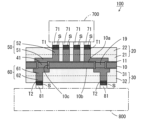
- FIG. 1 is a schematic cross-sectional view showing the configuration of a rewiring board according to one embodiment of the present invention.
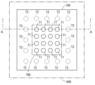
- 2 is a schematic plan view of the rewiring board of FIG. 1.
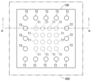
- FIG. 3 is a schematic bottom view of the rewiring board of FIG. 1.
- FIG. 4A and 4B are schematic cross-sectional views for explaining a first example of a method for manufacturing the rewiring board of FIG. 5A and 5B are schematic cross-sectional views for explaining a first example of a method for manufacturing the rewiring board of FIG. 6A to 6C are schematic cross-sectional views for explaining a first example of the method for manufacturing the rewiring board of FIG.
- FIG. 7A to 7C are schematic cross-sectional views for explaining a first example of the method for manufacturing the rewiring board of FIG. 8A to 8D are schematic cross-sectional views for explaining a first example of the method for manufacturing the rewiring board of FIG. 9A and 9B are schematic cross-sectional views for explaining a first example of the method for manufacturing the rewiring board of FIG. 10A and 10B are schematic cross-sectional views for explaining a first example of a method for manufacturing the rewiring board of FIG. 11A and 11B are schematic cross-sectional views for explaining a first example of the method for manufacturing the rewiring board of FIG.
- FIG. 12A and 12B are schematic cross-sectional views for explaining a first example of a method for manufacturing the rewiring board of FIG. 13A and 13B are schematic cross-sectional views for explaining a first example of the method for manufacturing the rewiring board of FIG. 14A and 14B are schematic cross-sectional views for explaining a first example of a method for manufacturing the rewiring board of FIG. 15A and 15B are schematic cross-sectional views for explaining a first example of a method for manufacturing the rewiring board of FIG. 16A and 16B are schematic cross-sectional views for explaining a first example of a method for manufacturing the rewiring board of FIG.
- FIG. 17A and 17B are schematic cross-sectional views for explaining a second example of the method for manufacturing the rewiring board of FIG. 18A and 18B are schematic cross-sectional views for explaining a second example of the method for manufacturing the rewiring board of FIG. 19A and 19B are schematic cross-sectional views for explaining a second example of the method for manufacturing the rewiring board of FIG. 20A to 20C are schematic cross-sectional views for explaining a second example of the method for manufacturing the rewiring board of FIG.
- FIG. 21 is a schematic cross-sectional view for explaining a second example of the method for manufacturing the rewiring board of FIG. 22A to 22C are schematic cross-sectional views for explaining a second example of the method for manufacturing the rewiring board of FIG.
- FIG. 23A to 23C are schematic cross-sectional views for explaining a second example of the method for manufacturing the rewiring board of FIG.
- FIG. 24 is a schematic cross-sectional view showing a first configuration example of a rewiring board in consideration of reduction of variations in height positions of a plurality of terminal portions.
- 25 is a plan view showing the positional relationship among the first terminal portion, the first connection conductor portion, the second terminal portion, the second connection conductor portion, the metal support and the via conductors in FIG. 24.
- FIG. FIG. 26 is a diagram showing an example of mounting a semiconductor element on the rewiring board of FIG. 27A to 27C are schematic cross-sectional views for explaining an example of a method for manufacturing the rewiring board of FIG.
- 28A and 28B are schematic cross-sectional views for explaining an example of a method for manufacturing the rewiring board of FIG. 29A and 29B are schematic cross-sectional views for explaining an example of a method for manufacturing the rewiring board of FIG. 30A to 30C are schematic cross-sectional views for explaining an example of a method for manufacturing the rewiring board of FIG. 31A to 31C are schematic cross-sectional views for explaining an example of a method for manufacturing the rewiring board of FIG. 32A to 32C are schematic cross-sectional views for explaining an example of a method for manufacturing the rewiring board of FIG. 33A to 33C are schematic cross-sectional views for explaining an example of a method for manufacturing the rewiring board of FIG.
- FIG. 34A and 34B are schematic cross-sectional views for explaining an example of a method for manufacturing the rewiring board of FIG.
- FIG. 35 is a schematic cross-sectional view showing a second configuration example of a rewiring board in which variations in height positions of a plurality of terminal portions are reduced.
- FIG. 36 is a schematic cross-sectional view showing a third configuration example of a rewiring board in which variations in height positions of a plurality of terminal portions are reduced.
- FIG. 37 is a schematic cross-sectional view showing a fourth configuration example of a rewiring board in which variations in height positions of a plurality of terminal portions are reduced.
- FIG. 38 is a schematic cross-sectional view of a rewiring board provided with an adhesion enhancing layer.
- a wired circuit board and a manufacturing method thereof according to an embodiment of the present invention will be described below with reference to the drawings.
- a rewiring board will be described as an example of the wiring circuit board.
- a rewiring board is arranged between an electronic component such as a semiconductor element and another wiring circuit board such as a rigid printed wiring circuit board (hereinafter abbreviated as a rigid board), and is used to connect fine patterns of the electronic component and other components. It plays a role of converting the pitch from the rough pattern of the wiring circuit board.
- a rewiring board is also called an interposer board.
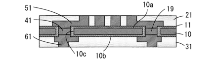
- FIG. 1 is a schematic cross-sectional view showing the configuration of a rewiring board according to an embodiment of the present invention.
- FIG. 2 is a schematic plan view of the rewiring board 100 of FIG.
- FIG. 3 is a schematic bottom view of the rewiring board 100 of FIG.
- FIG. 1 represents a cross section taken along line AA of FIGS. 2 and 3.
- FIG. 1 the rewiring board 100 mainly comprises a metal support 10, insulating layers 20 and 30, and conductor layers 50 and 60, and has a thickness of 60 ⁇ m or more and 500 ⁇ m or less. Also, the rewiring board 100 is arranged between the semiconductor element 700 and the rigid board 800 .
- the semiconductor element 700 has a plurality of electrode pads 71 and the rigid substrate 800 has a plurality of electrode pads 81 .
- the semiconductor element 700 is indicated by a one-dot chain line
- the rigid substrate 800 is indicated by a two-dot chain line.
- the metal support 10 is, for example, a metal or alloy containing one or more elements selected from the group consisting of copper, aluminum, iron, nickel, chromium, titanium and molybdenum.
- the metal support 10 is made of stainless steel and formed into a plate shape.
- the surface of the metal support 10 facing the semiconductor element 700 (the surface facing upward in FIG. 1) is referred to as the upper surface 10a
- the surface of the metal support 10 facing the rigid substrate 800 (the surface facing downward in FIG. 1) is referred to as the lower surface. 10b.
- the upper surface 10a and the lower surface 10b according to the present embodiment are parallel to each other, perpendicular to the thickness direction of the metal support 10, and flat.
- the direction in which the upper surface 10a of the metal support 10 faces is the upper side of the rewiring board 100
- the direction in which the lower surface 10b of the metal support 10 faces is the lower side of the rewiring board 100.
- the metal support 10 is not limited to the above examples, and 42 alloy, Invar alloy, or the like may be used.
- an Invar alloy is used for the metal support 10
- the coefficient of linear expansion of the metal support 10 can be adjusted according to changes in the composition of nickel (Ni) in the Invar alloy. In this case, it is possible to suppress the occurrence of warpage in each layer constituting the rewiring board 100 .
- the metal support 10 preferably has a thermal conductivity higher than that of the insulating layers 20 and 30. For example, it has a thermal conductivity of 10 W/mK or more and 400 W/mK or less. . Moreover, the metal support 10 preferably has a thickness of 10 ⁇ m or more and 100 ⁇ m or less, and more preferably has a thickness of 20 ⁇ m or more and 50 ⁇ m or less. Furthermore, the linear expansion coefficient of the metal support 10 at 25° C. to 200° C. is 0 ⁇ m/K or more and 25 ⁇ m/K or less.
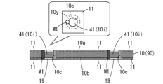
- a plurality of via holes 19 are formed in the metal support 10 .
- Each of the plurality of via holes 19 of the present example has a circular or rectangular opening when viewed from above in the thickness direction of the rewiring board 100 (vertical direction of the rewiring board 100).
- the maximum dimension of the opening of each via hole 19 perpendicular to the thickness direction of the rewiring board 100 is, for example, 10 ⁇ m or more and 250 ⁇ m or less.
- the above maximum dimension refers to the maximum dimension of the inner diameter of the via hole 19 when the opening of the via hole 19 has a circular shape in a plan view, for example.
- the maximum dimension of the diagonal line of the opening of the via hole 19 is used.
- a coating layer 11 is formed on the outer surface of the metal support 10 . More specifically, in metal support 10 , coating layer 11 is formed so as to entirely cover upper surface 10 a , lower surface 10 b and inner peripheral surface 10 c of each via hole 19 .
- the covering layer 11 is made of, for example, an organic insulating material.
- the organic insulating material of the covering layer 11 is, for example, photosensitive polyimide.
- the organic insulating material of the covering layer 11 is, for example, photosensitive polyimide.
- the coating layer 11 has a thickness of 1 ⁇ m or more and 10 ⁇ m or less.
- the coating layer 11 may be formed of other organic insulating materials such as acrylic resin, polyethernitrile resin, polyethersulfone resin, epoxy resin, polyethylene terephthalate resin, polyethylene naphthalate resin, or polyvinyl chloride resin.
- an inorganic insulating material can be used instead of the above organic insulating material.
- silicon carbide, silicon dioxide, aluminum nitride, aluminum oxide, or the like can be used as the material of the coating layer 11 .
- the coating layer 11 can be formed using a film forming technique such as sputtering or chemical vapor deposition, as described later.
- the thickness of the coating layer 11 is the same as the thickness (1 ⁇ m or more and 10 ⁇ m or less) when using photosensitive polyimide. can be made even smaller.
- a first insulating layer 21 and a second insulating layer 22 having a predetermined pattern are laminated in this order on the upper surface 10a of the metal support 10 .
- An insulating layer 20 is formed by a first insulating layer 21 and a second insulating layer 22 .
- a third insulating layer 31 and a fourth insulating layer 32 having a predetermined pattern are laminated in this order on the lower surface 10b of the metal support 10.
- An insulating layer 30 is formed by a third insulating layer 31 and a fourth insulating layer 32 .
- the insulating layers 20 and 30 are made of, for example, photosensitive polyimide.
- the insulating layers 20 and 30 may be made of other resin such as acrylic resin, polyethernitrile resin, polyethersulfone resin, epoxy resin, polyethylene terephthalate resin, polyethylene naphthalate resin, or polyvinyl chloride resin.
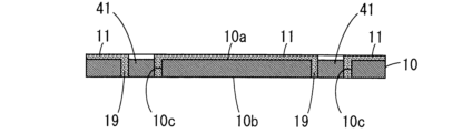
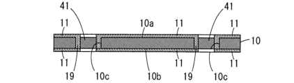
- a via conductor 41 is provided in each via hole 19 of the metal support 10 with the coating layer 11 interposed therebetween.
- via conductor 41 is made of the same metal as metal support 10 .
- a first conductor layer 51 is formed on the upper surface 10 a of the metal support 10 in addition to the first insulating layer 21 . Specifically, on the upper surface 10 a of the metal support 10 , the first insulating layer 21 non-formation region (region having a pattern opposite to the pattern of the first insulating layer 21 ) is coated with the coating layer 11 interposed therebetween.
- a first conductor layer 51 is formed. A portion of first conductor layer 51 is electrically connected to via conductor 41 .
- Each of the plurality of via conductors 41 of this example has a shape similar to the opening of the via hole 19 in which the via conductor 41 is provided, for example, in plan view in the thickness direction of the rewiring board 100 .
- the maximum dimension of each via conductor 41 perpendicular to the thickness direction of the rewiring board 100 is, for example, 5 ⁇ m or more and 200 ⁇ m or less.
- a second insulating layer 22 non-formation region (a region having a pattern opposite to the pattern of the second insulating layer 22) is provided with a second A conductor layer 52 is formed. A portion of the second conductor layer 52 is electrically connected to the first conductor layer 51 .
- a conductor layer 50 is formed by a first conductor layer 51 and a second conductor layer 52 .
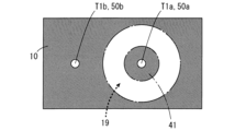
- the second conductor layer 52 has a plurality of terminal portions T1 exposed upward in regions where the second insulating layer 22 is not formed.
- a plurality of electrode pads 71 of the semiconductor element 700 are connected via solder S to these terminal portions T1. Therefore, the number and arrangement of the plurality of terminal portions T1 are determined so as to correspond to the number and arrangement of the plurality of electrode pads 71 of the semiconductor element 700.
- a third conductor layer 61 is formed in addition to the third insulating layer 31. Specifically, on the lower surface 10 b of the metal support 10 , the third insulating layer 31 non-formation region (region having a pattern opposite to the pattern of the third insulating layer 31 ) is coated with the coating layer 11 interposed therebetween. A third conductor layer 61 is formed. Part of third conductor layer 61 is electrically connected to via conductor 41 .
- a fourth insulating layer 32 non-formation region (a region with a pattern opposite to the pattern of the fourth insulating layer 32) is provided with a fourth A conductor layer 62 is formed.
- a portion of the fourth conductor layer 62 is electrically connected to the third conductor layer 61 .
- a conductor layer 60 is formed by the third conductor layer 61 and the fourth conductor layer 62 .
- the fourth conductor layer 62 is formed with a plurality of terminal portions T2 exposed downward in regions where the fourth insulating layer 32 is not formed.
- a plurality of electrode pads 81 of the rigid substrate 800 are connected via solder S to these terminal portions T2. Therefore, the number and arrangement of the plurality of terminal portions T2 are determined so as to correspond to the number and arrangement of the plurality of electrode pads 81 of the rigid substrate 800.
- the conductor layers 50 and 60 are made of copper.
- Conductor layers 50 and 60 are made of a metal or alloy containing one or more of copper, gold, silver, platinum, lead, tin, nickel, cobalt, indium, rhodium, chromium, tungsten, ruthenium, and the like. may
- each of the plurality of terminal portions T1 and T2 has a laminated structure of a nickel film and a gold plating film.
- each terminal portion T1 has a structure in which a nickel film and a gold plating film are formed in this order on the surface of the upper end portion of the second conductor layer 52 .
- Each terminal portion T2 has a structure in which a nickel film and a gold plating film are formed in this order on the surface of the lower end portion of the fourth conductor layer 62 .
- each of the terminal portions T1 and T2 may be composed only of a gold-plated film without the nickel film. Corrosion resistance of each of the terminal portions T1 and T2 is ensured by the gold plating film.
- each terminal portion T1 may be composed of the conductor layer 50 (second conductor layer 52) itself, or may have a structure in which the surface of the upper end portion of the second conductor layer 52 is subjected to antirust treatment.
- each terminal portion T2 may be composed of the conductor layer 60 (fourth conductor layer 62) itself, or may have a structure in which the surface of the lower end portion of the fourth conductor layer 62 is subjected to antirust treatment. You may
- each of the plurality of terminal portions T1 formed on the upper surface of the rewiring board 100 is formed on the lower surface of the rewiring board 100 through the plurality of via conductors 41 and the conductor layers 50 and 60. It is electrically connected to one of the plurality of terminal portions T2.
- a plurality of electrode pads 71 of the semiconductor element 700 are connected to the plurality of terminal portions T1 of the rewiring substrate 100, and a plurality of electrode pads 81 of the rigid substrate 800 are connected to the plurality of terminal portions T2 of the rewiring substrate 100. be done. Thereby, the plurality of electrode pads 71 of the semiconductor element 700 and the plurality of electrode pads 81 of the rigid substrate 800 are electrically connected through the rewiring substrate 100 .
- the number of terminal portions T1 located on the top surface of the rewiring board 100 and the number of terminal portions T2 located on the bottom surface of the rewiring board 100 are different. , but the invention is not limited to this. The number of terminal portions T1 located on the top surface of the rewiring board 100 and the number of terminal portions T2 located on the bottom surface of the rewiring board 100 do not have to match.
- FIGS. It is a cross-sectional view. Schematic cross-sectional views shown in FIGS. 4 to 16 correspond to the schematic cross-sectional view of FIG. 7, 9 and 10 of FIGS. 4 to 16 show, in addition to the schematic cross-sectional views, partial enlarged plan views of the object (intermediate body of the rewiring board 100) in balloons.
- the rewiring board 100 of this example is manufactured by a roll-to-roll method.
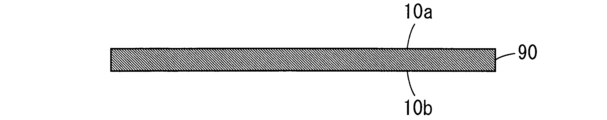
- a roll around which a long metal plate 90 made of stainless steel is wound (hereinafter referred to as a delivery roll) is prepared.
- a metal plate 90 is delivered from the prepared delivery roll.
- the metal plate 90 delivered from the delivery roll is wound around another roll.
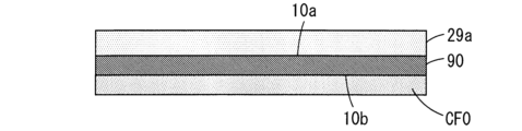
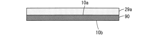
- FIG. 4 shows a partial cross-section of the metal plate 90 delivered from the delivery roll.
- Metal plate 90 is a member for forming metal support 10 described above, and has upper surface 10a and lower surface 10b. According to the roll-to-roll method, the following processes are sequentially performed on each area of the metal plate 90 while the long metal plate 90 moves in the longitudinal direction.
- a carrier film CF0 is attached onto the lower surface 10b of the metal plate 90.
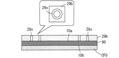
- a photosensitive dry film resist 29a is applied on the upper surface 10a of the metal plate 90.
- the photosensitive dry film resist 29a is exposed in a predetermined pattern and developed to form an etching resist 29b on the upper surface 10a of the metal plate 90, as shown in FIG.
- the etching resist 29b of this example has a plurality of annular openings 29x surrounding a plurality of portions of the metal plate 90 in plan view in the thickness direction of the metal plate 90, as shown in the balloons in FIG. have.
- a plurality of portions of the upper surface 10a of the metal plate 90 overlapping the plurality of openings 29x of the etching resist 29b are exposed upward.
- Each of the plurality of openings 29x of the etching resist 29b is an opening for forming the via hole 19 of FIG.
- a plurality of portions of the metal plate 90 exposed through the plurality of openings 29x of the etching resist 29b are etched. Further, as shown in FIG. 9, the etching resist 29b is removed from the upper surface 10a of the metal plate 90. Then, as shown in FIG. By forming a plurality of via holes 19 in the metal plate 90 in this manner, the metal support 10 is formed. At this time, as shown in the balloon of FIG. 9, inside the via hole 19, a part of the metal plate 90 is formed in the shape of an island as the via conductor 41 so as not to come into contact with the inner peripheral surface 10c of the via hole 19. .
- the covering layer 11 made of photosensitive polyimide is formed on the exposed upper surface 10a and the inner peripheral surface 10c of the metal support 10 except for the upper surface of the via conductors 41. Then, as shown in FIG. Specifically, the formation of the coating layer 11 is performed as follows.
- a precursor of photosensitive polyimide is applied onto the upper surface 10a of the metal support 10 .
- the region between the inner peripheral surface 10c of the via hole 19 and the outer peripheral surface of the via conductor 41 is filled with a photosensitive polyimide precursor.
- the coated photosensitive polyimide precursor is exposed and developed to form coating layer 11 except for the upper surface portions of via conductors 41 .
- the formed coating layer 11 is cured.
- the coating layer 11 is formed by sputtering, for example.
- silicon carbide or aluminum oxide is used as the material of the coating layer 11, the coating layer 11 is formed by chemical vapor deposition, for example.
- the carrier film CF0 is peeled off from the lower surface 10b of the metal support 10.
- covering layer 11 made of photosensitive polyimide is formed on exposed lower surface 10 b of metal support 10 excluding the lower surface portions of via conductors 41 .
- the formation of the coating layer 11 on the lower surface 10b of the metal support 10 is performed in the same manner as the formation of the coating layer 11 on the upper surface 10a of the metal support 10 .
- the formed coating layer 11 is cured.
- a first conductor layer 51 made of copper is formed in predetermined regions on the upper surfaces of the plurality of via conductors 41 and the upper surface 10 a of the metal support 10 . Furthermore, a third conductor layer 61 made of copper is formed in predetermined regions on the lower surface of the plurality of via conductors 41 and the lower surface 10 b of the metal support 10 . Specifically, the first conductor layer 51 and the third conductor layer 61 are formed as follows.
- a seed layer composed of, for example, a chromium thin film and a copper thin film is formed by sputtering or electroless plating on the upper surface 10a of the metal support 10, the lower surface 10b of the metal support 10, the upper surface of the via conductor 41, and the lower surface of the via conductor 41. be done.
- a plating resist having a predetermined pattern is formed on the seed layer.
- parts of the first conductor layer 51 and the third conductor layer 61 are formed by electroplating on the seed layer exposed through the openings of the plating resist.
- the first conductor layer 51 is electrically connected to the plurality of via conductors 41 .
- the third conductor layer 61 is electrically connected to the plurality of via conductors 41 .
- the portions of the first conductor layer 51 and the third conductor layer 61 formed here are used as wiring portions.
- the first conductor layer 51 and the third conductor layer 61 include via portions in addition to the wiring portions described above. Therefore, after forming the wiring portions of the first conductor layer 51 and the third conductor layer 61, the via portions of the first conductor layer 51 and the third conductor layer 61 are further formed by electroplating using a plating resist. be done.
- the plating resist is peeled off, and the exposed portions of the seed layer (the portions where the first conductor layer 51 and the third conductor layer 61 are not formed) are removed by etching. Furthermore, a barrier layer is formed on the outer surfaces of the first conductor layer 51 and the third conductor layer 61 to suppress the diffusion of copper.
- the barrier layer is made of, for example, a nickel thin film. It should be noted that illustration of the seed layer and the barrier layer is omitted in FIG.
- a photosensitive polyimide is applied to a region of the upper surface 10a of the metal support 10 where the first conductor layer 51 is not formed.
- a first insulating layer 21 is formed.
- the first insulating layer 21 is also formed in the region of the wiring portion of the first conductor layer 51 .
- the wiring portion of the first conductor layer 51 is covered with the first insulating layer 21, and the via portion (portion other than the wiring portion) of the first conductor layer 51 is exposed.
- a third insulating layer 31 made of photosensitive polyimide is formed in a region of the lower surface 10b of the metal support 10 where the third conductor layer 61 is not formed.
- the third insulating layer 31 is also formed in the region of the wiring portion of the third conductor layer 61 .
- the wiring portion of the third conductor layer 61 is covered with the third insulating layer 31, and the via portion (portion other than the wiring portion) of the third conductor layer 61 is exposed.
- the first insulating layer 21 and the third insulating layer 31 are formed by applying a photosensitive polyimide precursor to the upper surface 10a and the lower surface 10b of the metal support 10, and exposing and developing the precursor. . Further, the formed first insulating layer 21 and third insulating layer 31 are cured.
- the barrier layer existing in a predetermined region on the upper surface of the first conductor layer 51 is removed. Also, the barrier layer present in a predetermined region on the upper surface of the third conductor layer 61 is removed.
- a second conductor layer 52 is formed in a predetermined region on the upper surface of the first conductor layer 51 and the upper surface of the first insulating layer 21 from which the barrier layer has been removed.
- a fourth conductor layer 62 is formed in a predetermined region on the lower surface of the third conductor layer 61 and the lower surface of the third insulating layer 31 from which the barrier layer has been removed.
- Each of the second conductor layer 52 and the fourth conductor layer 62 has a wiring portion and a via portion similarly to the first conductor layer 51 and the third conductor layer 61 . Therefore, the formation of the second conductor layer 52 and the fourth conductor layer 62 is basically performed in the same procedure as the formation of the first conductor layer 51 and the third conductor layer 61 .
- a second insulating layer made of photosensitive polyimide is formed on the upper surfaces of the first insulating layer 21 and the first conductive layer 51 where the second conductive layer 52 is not formed. 22 are formed.
- the second insulating layer 22 is also formed in the region of the wiring portion of the second conductor layer 52 .
- the wiring portion of the second conductor layer 52 is covered with the second insulating layer 22, and the via portion (portion other than the wiring portion) of the second conductor layer 52 is exposed.
- the fourth insulating layer 32 made of photosensitive polyimide is formed on the lower surfaces of the third insulating layer 31 and the third conductive layer 61 in areas where the fourth conductive layer 62 is not formed.
- the fourth insulating layer 32 is also formed in the region of the wiring portion of the fourth conductor layer 62 .
- the wiring portion of the fourth conductor layer 62 is covered with the fourth insulating layer 32, and the via portion (portion other than the wiring portion) of the fourth conductor layer 62 is exposed.
- the second insulating layer 22 and the fourth insulating layer 32 are basically formed in the same procedure as the first insulating layer 21 and the third insulating layer 31 are formed.
- the barrier layer formed on the plurality of portions exposed upward of the second conductor layer 52 is removed, and the terminal portions T1 are formed on the plurality of portions of the second conductor layer 52 from which the barrier layer has been removed. (FIG. 1) is formed.
- the barrier layer formed on the plurality of portions exposed downward of the fourth conductor layer 62 is removed, and the terminal portions T2 ( 1) is formed.
- the terminal portions T1 and T2 have a laminated structure of, for example, a nickel film and a gold plating film. Note that the terminal portions T1 and T2 may be formed only of the gold plating film. Thus, the rewiring board 100 is completed.
- the carrier film CF0 attached to the metal plate 90 in the initial process may be made of a photosensitive material such as photosensitive polyimide.
- the carrier film CF0 is exposed and developed to form the coating layer 11 on the lower surface 10b of the metal support 10. can be formed. Therefore, it becomes unnecessary to peel off the carrier film CF0.
- FIGS. 17 to 23 are schematic cross-sectional views for explaining a second example of manufacturing method of the rewiring board 100 of FIG.
- the schematic cross-sectional views shown in FIGS. 17-23 correspond to the schematic cross-sectional view of FIG. 1, as do the schematic cross-sectional views of FIGS. 4-16. 18, 20, 21, 22 and 23 out of FIGS. 17 to 23, in addition to the schematic cross-sectional views, one part of the object (the intermediate of the rewiring board 100) is shown in the balloon. A partial enlarged plan view is shown.
- the second example of the method for manufacturing the rewiring board 100 will be described below mainly on the differences from the first example of the method for manufacturing the rewiring board 100 .
- the rewiring board 100 of this example is manufactured by the roll-to-roll method as in the first example. Therefore, also in this example, first, a pay-out roll around which the long metal plate 90 made of stainless steel is wound is prepared. A metal plate 90 is delivered from a prepared delivery roll, and the delivered metal plate 90 is wound around another roll. Each region of the metal plate 90 moving from the supply roll to another roll is sequentially subjected to the following processes.
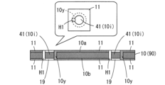
- a photosensitive dry film resist 29a is adhered to the upper surface 10a of the metal plate 90, as shown in FIG. Attached. Thereafter, the photosensitive dry film resist 29a is exposed in a predetermined pattern and developed to form an etching resist 29b on the upper surface 10a of the metal plate 90, as shown in FIG.
- the etching resist 29b of this example has a plurality of arcuate openings 29y in plan view in the thickness direction of the metal plate 90, as shown in the balloons in FIG. As a result, a plurality of portions of the upper surface 10a of the metal plate 90 overlapping the plurality of openings 29y of the etching resist 29b are exposed upward.
- Each of the plurality of openings 29y is an opening for forming the via hole 19 of FIG.
- the shape of each of the plurality of openings 29y in this example is close to an annular shape in a plan view.
- a plurality of portions of the metal plate 90 exposed through the plurality of openings 29y of the etching resist 29b are etched.
- the etching resist 29b is removed from the upper surface 10a of the metal plate 90. Then, as shown in FIG.
- a plurality of arc-shaped openings 10y are formed in the metal plate 90, as shown in the balloon in FIG.
- the conductor forming portion 10i and the connecting portion 10j are formed in the region of the metal plate 90 where each opening 10y is formed.
- the connecting portion 10j is a portion located between one end and the other end of the opening 10y extending in an arc shape in plan view.
- the conductor forming portion 10i is a portion surrounded by the opening portion 10y and the connecting portion 10j in plan view.
- the conductor forming portion 10i and the connecting portion 10j are indicated by dashed lines.
- the above conductor forming portion 10i is finally separated from other portions of the metal plate 90 to be used as the via conductor 41 .
- the connecting portion 10j is integrally formed with other portions of the metal plate 90.
- the metal plate 90 including the plurality of conductor forming portions 10i can be transported independently by the roll-to-roll method without using the carrier film CF0.
- a covering layer 11 made of photosensitive polyimide is formed on the exposed upper and lower surfaces 10a and 10b of the metal plate 90 except for the upper and lower surfaces of the plurality of conductor forming portions 10i of the metal plate 90. be done. Also, the coating layer 11 is formed in the plurality of openings 10y of the metal plate 90 .
- a photosensitive polyimide precursor is applied onto the upper surface 10 a and the lower surface 10 b of the metal plate 90 . Further, the inside of each opening 10y of the metal plate 90 is filled with a photosensitive polyimide precursor. Thereafter, the coated photosensitive polyimide precursor is exposed and developed to form the coating layer 11 on the entire surface of the metal plate 90 except for the upper and lower surfaces of the conductor forming portion 10i. The formed coating layer 11 is cured.
- the multiple connecting portions 10j of the metal plate 90 are removed.
- the plurality of connecting portions 10j can be removed by forming through holes H1 in the portion of the metal plate 90 including the connecting portions 10j using a laser processing technique. In this manner, a plurality of via holes 19 each having openings 10y and through holes H1 are formed in metal plate 90.
- the metal plate 90 is formed as the metal support 10 . Formation of the through holes H1 for removing the plurality of connecting portions 10j may be performed using, for example, a drilling technique or a punching technique.
- an insulating material MI is embedded inside the plurality of through holes H1 formed to remove the plurality of connecting portions 10j.
- an insulating filler such as silicon carbide, silicon dioxide or aluminum nitride is used.
- each conductor forming portion 10i is electrically isolated from the inner peripheral surface 10c of the via hole 19 by the covering layer 11 and the insulating material MI. Thereby, each conductor forming portion 10i can be used as a via conductor 41 in each via hole 19 in which the conductor forming portion 10i is accommodated.
- a conductor layer 50 and an insulating layer 20 are formed above the metal support 10 shown in FIG.
- a conductor layer 60 and an insulating layer 30 are formed below the metal support 10 shown in FIG. 23 in the same procedure as in the first example of the method for manufacturing the rewiring board 100 .
- At least a portion of the first conductor layer 51 is electrically connected to the upper surfaces of the plurality of via conductors 41 exposed upward when the conductor layer 50 is formed.
- formed to connect to At least part of the third conductor layer 61 is formed so as to be electrically connected to the lower surfaces of the plurality of via conductors 41 exposed downward.
- the insulating material MI is used in addition to the covering layer 11 in order to electrically separate the metal support 10 and the via conductors 41 from each other. Therefore, according to the configuration of the rewiring board 100 manufactured according to the second example, the insulating material MI is added in the via hole 19 of the metal support 10 in the cross-sectional view of FIG.
- the via made of a part of the metal plate 90 is placed in the via hole 19 so as not to contact the inner peripheral surface 10c of the via hole 19.
- a conductor 41 is formed.
- the via conductors 41 in the via holes 19 are made of a part of the metal plate 90, there is no need to form the via conductors 41 in the via holes 19 by plating or the like. Therefore, it is easy to form the via conductor 41 in the via hole 19 .
- the rewiring board 100 that is easy to manufacture and has improved electrical continuity reliability is realized.
- photosensitive polyimide for example, is used as the material of the coating layer 11 that covers the surface of the metal support 10 .
- the coating layer 11 can be easily formed on a desired region of the surface of the metal support 10 by using a photolithographic technique.
- the coating layer 11 is formed over substantially the entire surface of the metal support 10 in the above example, the coating layer 11 may be selectively formed on a part of the surface of the metal support 10. good.
- the coating layer 11 includes the inner peripheral surface 10c of the via hole 19 of the metal support 10, the formation region of the first conductor layer 51 on the upper surface 10a of the metal support 10, and the third portion of the lower surface 10b of the metal support 10. may be formed only in the region where the conductor layer 61 is formed.
- the linear expansion coefficient of the metal support 10 at 25°C to 200°C is 0 ⁇ m/K or more and 25 ⁇ m/K or less. In this case, it is possible to prevent the metal support 10 from greatly deforming due to a change in the temperature of the rewiring board 100 . Thereby, the reliability of the rewiring board 100 is improved.
- the metal support 10 preferably contains a component that improves adhesion between the metal support 10 and the coating layer 11 .
- a component that improves adhesion between the metal support 10 and the coating layer 11 peeling of the coating layer 11 from the surface of the metal support 10 is suppressed.
- Components that improve adhesion between the metal support 10 and the coating layer 11 include copper, aluminum, nickel, chromium, titanium, molybdenum, and the like.
- a semiconductor element 700 includes a plurality of electrode pads 71 as a plurality of terminals.
- the plurality of electrode pads 71 are basically formed such that the tips of the plurality of electrode pads 71 (electrical connection portions with respect to the rewiring board 100) are positioned on one plane.
- the semiconductor element 700 cannot be mounted on the rewiring board 100. less reliable.
- the rewiring board 100 may be mounted on the rewiring board 100 in an unintended orientation.
- the tip of each electrode pad 71 of the semiconductor element 700 has a circular exposed surface with a diameter of about 30 ⁇ m, for example.
- the semiconductor element 700 is mounted on the rewiring board 100 , hemispherical solder S is provided in advance on the exposed surface of the tip of each electrode pad 71 . Therefore, the solder S provided on each electrode pad 71 protrudes from the tip of the electrode pad 71 by about 15 ⁇ m. Therefore, the rewiring board 100 needs to be formed so that the variation in the height positions of the plurality of terminal portions T1 is at least 15 ⁇ m or less.
- the rewiring board 100 is preferably formed so that the height positional variation of the plurality of terminal portions T1 is 10 ⁇ m or less. Further, the rewiring board 100 is more preferably formed so that the variation in the height position of the plurality of terminal portions T1 is 5 ⁇ m or less, and the variation in the height position of the plurality of terminal portions T1 is 2 ⁇ m or less. It is further preferred that it is formed as follows.
- ⁇ 2> Causes of Variation in Height Positions of Plurality of Terminals T1 Causes of variation in height positions of a plurality of terminals T1 are examined.
- One or a plurality of terminal portions T1 overlapping the via conductors 41 in a plan view are formed by directly forming a conductor layer 50 on the upper surface of the via conductors 41 at the same height as the upper surface 10a of the metal support 10, for example. It is formed.
- one or more terminal portions T1 which do not overlap the via conductors 41 in plan view are formed by forming a conductor layer 50 on the upper surface 10a of the metal support 10 excluding the via conductors 41 with the covering layer 11 interposed therebetween. be done.
- variations in the height positions of the plurality of terminal portions T1 are mainly due to one or more terminal portions T1 overlapping the via conductors 41 in plan view and one or more terminal portions T1 not overlapping the via conductors 41 in plan view. occurs between In consideration of this point, the rewiring board 100 has the configuration (first to fourth configuration examples) described below so that the variation in the height positions of the plurality of terminal portions T1 is at least 15 ⁇ m or less. You may In addition, in the first to fourth configuration examples described below, each of the plurality of terminal portions T1 is formed of the conductor layer 50 itself.
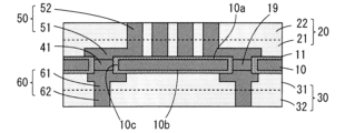
- FIG. 1 is a schematic cross-sectional view showing a configuration example of No. 1.
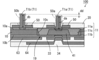
- FIG. FIG. 24 shows an enlarged portion of the rewiring board 100 according to the first configuration example.
- a rewiring board 100 in FIG. 24 has a metal support 10 in which via holes 19 are formed.
- the via hole 19 is indicated by a thick dotted line frame.
- a via conductor 41 made of the same metal as the metal support 10 is formed in the via hole 19 of the metal support 10 .
- a coating layer 11 is formed so as to cover the upper surface 10 a and the lower surface 10 b of the metal support 10 and the inner peripheral surface 10 c of the via hole 19 of the metal support 10 .
- a portion of the coating layer 11 that covers the upper surface 10a of the metal support 10 is called an upper surface coating portion 11a.
- a portion of the coating layer 11 that covers the lower surface 10b of the metal support 10 is called a lower surface covering portion 11b.
- a portion of the coating layer 11 that covers the inner peripheral surface 10c of the metal support 10 is called an in-hole coating portion 11c.
- In-hole covering portion 11 c is located inside via hole 19 in plan view and surrounds via conductor 41 .
- a plurality of conductor layers 50 having a predetermined pattern are formed on the upper surface covering portion 11a of the covering layer 11 .
- An insulating layer 20 is formed so as to partially cover each conductor layer 50 .
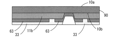
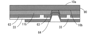
- a plurality of (two in this example) conductor layers 63 and 64 and a plurality of (two in this example) insulating layers 33 and 34 having a predetermined pattern are laminated on the lower surface covering portion 11b of the covering layer 11. ing.
- one conductor layer 50 among the plurality of conductor layers 50 includes a first connection conductor portion 50a.
- the first connection conductor portion 50 a is in contact with the via conductor 41 and extends upward from the via conductor 41 toward the rewiring board 100 . That is, the first connection conductor portion 50a extends from the via conductor 41 in the direction in which the upper surface 10a of the metal support 10 faces.
- a tip portion of the first connection conductor portion 50a constitutes a terminal portion T1.
- the terminal portion T1 formed by the tip portion of the first connection conductor portion 50a is referred to as the first terminal portion T1a.
- the other conductor layer 50 among the plurality of conductor layers 50 includes the second connection conductor portion 50b.
- the second connection conductor portion 50b is formed on the upper surface 10a of the metal support 10 via a portion of the upper surface covering portion 11a. Further, the second connection conductor portion 50b extends upward from the rewiring board 100 from a portion of the upper surface covering portion 11a. That is, the second connection conductor portion 50b extends from a portion of the upper surface covering portion 11a in the direction in which the upper surface 10a of the metal support 10 faces.
- a tip portion of the second connection conductor portion 50b constitutes a terminal portion T1.
- the terminal portion T1 formed by the tip portion of the second connection conductor portion 50b is referred to as the second terminal portion T1b.
- FIG. 25 shows the positional relationship among the first terminal portion T1a, the first connection conductor portion 50a, the second terminal portion T1b, the second connection conductor portion 50b, the metal support 10 and the via conductor 41 of FIG. It is a top view. Note that the scale of the plan view of FIG. 25 is different from the scale of the schematic cross-sectional view of FIG. As shown in FIG. 25, the first terminal portion T1a and the first connection conductor portion 50a overlap the via conductor 41 in plan view. On the other hand, the second terminal portion T1b and the second connection conductor portion 50b do not overlap the via conductor 41 in plan view.
- the vertical length (thickness) da of the first connection conductor 50a and the vertical length The length (thickness) db is almost the same. Therefore, the difference between the height position of the first terminal portion T1a and the height position of the second terminal portion T1b is the upper surface covering portion 11a located between the metal support 10 and the second connection conductor portion 50b. determined by the thickness of Therefore, in this example, the upper surface covering portion 11a is formed so that the thickness of the portion of the upper surface covering portion 11a where the second connection conductor portion 50b is formed is smaller than the thickness of the other portions. .
- FIG. 26 is a diagram showing an example of mounting the semiconductor element 700 on the rewiring board 100 of FIG. As shown in FIG. 26, a semiconductor element 700 is mounted from above the rewiring board 100 . At this time, the solder S is provided on each of the plurality of electrode pads 71 of the semiconductor element 700 as described above. The solder S protrudes from the tip of the electrode pad 71 by a predetermined length sh.
- the difference dd between the height position of the first terminal portion T1a and the height position of the second terminal portion T1b is the solder S provided on the plurality of electrode pads 71 of the semiconductor element 700.
- the thickness of the portion of the upper surface covering portion 11a that overlaps the second connection conductor portion 50b is adjusted so that the length sh is less than or equal to sh.
- the length sh of the solder S provided on the plurality of electrode pads 71 is 15 ⁇ m.
- the difference dd between the height positions of the first terminal portion T1a and the second terminal portion T1b is greater than the length sh (15 ⁇ m) of the solder S provided on the plurality of electrode pads 71.
- the semiconductor element 700 can be structurally stably mounted on the rewiring board 100 as compared with a large size. Further, in a state where the semiconductor element 700 is mounted on the rewiring board 100, the reliability of electrical continuity between the rewiring board 100 and the semiconductor element 700 is improved.
- the difference dd in the rewiring substrate 100 of the first configuration example is 10 ⁇ m or less. It is preferably 5 ⁇ m or less, more preferably 2 ⁇ m or less. In these cases, the reliability of mounting the semiconductor element 700 on the rewiring board 100 is further improved.
- FIGS. 4 to 16 are schematic cross-sectional views for explaining an example of a method of manufacturing the rewiring board 100 of FIG.
- the rewiring board 100 according to the first configuration example is manufactured by, for example, a roll-to-roll method in the same manner as the first example of the manufacturing method of the rewiring board 100 described with reference to FIGS. 4 to 16. .
- a delivery roll around which a long metal plate 90 made of stainless steel is wound is prepared, and the metal plate 90 is delivered from the prepared delivery roll.
- the delivered metal plate 90 is wound on another roll.
- the metal plate 90 like the metal plate 90 in FIG. 4, is a member for forming the metal support 10, and has an upper surface 10a and a lower surface 10b. While the metal plate 90 moves in the longitudinal direction, each area of the metal plate 90 is sequentially subjected to the following processes.
- the lower surface covering portion 11b is formed on the lower surface 10b of the metal plate 90 in a predetermined pattern.
- the lower surface covering portion 11b is made of a photosensitive material.
- the lower surface covering portion 11b can be easily patterned by selectively exposing the photosensitive material forming the lower surface covering portion 11b.
- photosensitive polyimide can be used as the photosensitive material.
- other photosensitive resins acrylic resin, epoxy resin, polyamide resin, polybenzoxazole resin, polyvinyl chloride resin, or other photosensitive resin
- photosensitive polyimide may also be used instead of photosensitive polyimide.
- a plurality of conductor layers 63 are formed in a predetermined pattern on one surface of the lower surface covering portion 11b exposed downward and on the portion of the metal plate 90 exposed downward. Further, as shown in FIG. 29, the insulating layer 33 is formed in a predetermined pattern on the lower surface covering portion 11b so as to cover at least a portion of the conductor layer 63. As shown in FIG. 28, a plurality of conductor layers 63 are formed in a predetermined pattern on one surface of the lower surface covering portion 11b exposed downward and on the portion of the metal plate 90 exposed downward. Further, as shown in FIG. 29, the insulating layer 33 is formed in a predetermined pattern on the lower surface covering portion 11b so as to cover at least a portion of the conductor layer 63. As shown in FIG.
- a plurality of conductor layers 64 are formed in a predetermined pattern on one surface of the insulating layer 33 exposed downward and on the portion of the conductor layer 63 exposed downward. Further, as shown in FIG. 31, an insulating layer 34 is formed in a predetermined pattern on the insulating layer 33 so as to cover at least part of the conductor layer 64 .
- the formation of the conductor layers 63, 64 is performed in the same procedure as the formation of the respective conductor layers (51, 52, 61, 62) in the method of manufacturing the rewiring board 100 described with reference to FIGS.
- the insulating layers 33 and 34 are formed in the same procedure as the insulating layers (21, 22, 31, 32) in the method of manufacturing the rewiring board 100 described with reference to FIGS. will be
- the metal plate 90 is formed with an annular opening 19x.
- the via hole 19 and the metal support 10 are formed by the annular opening 19x.
- the via holes 19 are formed by the same method as the formation of the via holes 19 in the manufacturing method of the rewiring board 100 described with reference to FIGS.
- a portion of metal plate 90 is formed in an island shape as via conductor 41 so as not to come into contact with inner peripheral surface 10 c of via hole 19 .
- the in-hole covering portion 11c is formed to cover the inner peripheral surface 10c of the via hole 19 on one surface of the lower surface covering portion 11b exposed upward. Further, an upper surface covering portion 11a is formed on the upper surface 10a of the metal support 10 in a predetermined pattern.
- the upper covering portion 11a is made of a photosensitive material, like the lower covering portion 11b.
- an opening h11 for exposing the upper surface of the via conductor 41 is formed at a position above the via conductor 41 where the first connection conductor portion 50a of FIG. 24 is to be formed.
- This opening h12 is formed using, for example, a gradation exposure technique.
- the thickness of the portion of the upper covering portion 11a where the opening h12 is formed is preferably 1 ⁇ m to 5 ⁇ m, and is 2 ⁇ m in this example. Further, in this example, the thickness of the portion of the upper covering portion 11a where the opening h12 is not formed is 10 ⁇ m.
- the maximum dimension of the opening h12 when viewed in plan is in the range of 10 ⁇ m or more and 50 ⁇ m or less than the design maximum dimension of the second terminal portion T1b when viewed in plan. It is preferably formed to be large.
- the opening h12 has a maximum dimension value larger than the design maximum dimension value of the second terminal portion T1b when viewed from above in a range of 15 ⁇ m or more and 40 ⁇ m or less.
- the opening h12 has a circular shape with a diameter of 40 ⁇ m in plan view or a circular shape with a diameter of 50 ⁇ m in plan view. It is preferably formed as follows. In this case, even if the formation positions of the plurality of conductor layers 50 are misaligned in the manufacturing process of the rewiring board 100, the misalignment is absorbed by the size of the openings h12.
- a plurality of conductor layers 50 are formed in a predetermined pattern on a plurality of predetermined regions of the exposed upper surface of the upper surface covering portion 11a and the portions of the via conductors 41 exposed through the openings h11. formed by
- the first connection conductor portion 50a is formed in the conductor layer 50 formed on the via conductor 41.
- a second connection conductor portion 50b is formed in the conductor layer 50 formed on the bottom portion of the opening h12 of the upper surface covering portion 11a.
- Each of the first connection conductor portion 50a and the second connection conductor portion 50b has a cylindrical shape extending in the vertical direction of the rewiring board 100, for example.
- the tip portions of the plurality of first connection conductor portions 50a constitute the first terminal portion T1a, and the tip portions of the plurality of second connection conductor portions 50b constitute the second terminal portion T1b.
- the vertical length (thickness) da of the first connection conductor portion 50a formed in this example and the vertical length (thickness) db of the second connection conductor portion 50b are the same (see FIG. 24). ).
- the insulating layer 20 is formed in a predetermined pattern on the upper surface covering portion 11a so as to partially cover each conductor layer 50 .
- the formation of the insulating layer 20 of this example is performed in the same procedure as the formation of the respective insulating layers (21, 22, 31, 32) in the manufacturing method of the rewiring board 100 described with reference to FIGS. As a result, the rewiring board 100 of FIG. 24 is completed.
- the thickness of the portion of the upper covering portion 11a where the opening h12 is formed is 2 ⁇ m, and the thickness of the portion of the upper covering portion 11a where the opening h12 is not formed is 10 ⁇ m.
- the difference dd (FIG. 26) between the height position of the first terminal portion T1a and the height position of the second terminal portion T1b is 8 ⁇ m.
- FIG. 2 is a schematic cross-sectional view showing a configuration example of No. 2.
- FIG. FIG. 35 shows an enlarged portion of the rewiring board 100 according to the second configuration example.
- the rewiring board 100 according to the second configuration example differences from the rewiring board 100 according to the first configuration example shown in FIG. 24 will be described.
- the total thickness of the upper surface covering portion 11a of the coating layer 11 is equal to the maximum thickness of the upper surface covering portion 11a according to the first configuration example. less than Specifically, the top covering portion 11a according to the second configuration example has a thickness of 15 ⁇ m or less, preferably 10 ⁇ m or less, more preferably 5 ⁇ m or less, and 2 ⁇ m or less. It is more preferable to have thickness.
- the first terminal A difference dd between the height position of the portion T1a and the height position of the second terminal portion T1b is equal to or less than 15 ⁇ m, which is the thickness of the upper surface covering portion 11a.
- the lower surface covering portion 11b is also formed to have approximately the same thickness as the upper surface covering portion 11a.
- the rewiring board 100 according to the second structural example is manufactured by the manufacturing method of FIGS. can be made in basically the same way.
- a precursor of photosensitive polyimide is applied onto the upper surface 10a of the metal support 10, and a precursor of the photosensitive polyimide is filled in the via hole 19. fill the body.
- the supply amount of the precursor is adjusted so that the thickness of the precursor applied onto the upper surface 10a of the metal support 10 is sufficiently small.
- the coated and filled photosensitive polyimide is exposed and developed to form the upper surface covering portion 11a having a small thickness.
- the upper surface covering portion 11a according to the second configuration example may be made of an inorganic insulating material such as silicon carbide, silicon dioxide, aluminum nitride or aluminum oxide instead of photosensitive resin such as photosensitive polyimide.
- the top covering portion 11a can be formed using a film forming technique such as sputtering or chemical vapor deposition.
- the difference dd in the rewiring substrate 100 of the second configuration example is It is preferably 10 ⁇ m or less, more preferably 5 ⁇ m or less, and even more preferably 2 ⁇ m or less. In these cases, the reliability of mounting the semiconductor element 700 on the rewiring board 100 is further improved.
- FIG. 3 is a schematic cross-sectional view showing a configuration example of No. 3.
- FIG. FIG. 36 shows an enlarged portion of the rewiring board 100 according to the third configuration example.
- the rewiring board 100 according to the third configuration example differences from the rewiring board 100 according to the first configuration example shown in FIG. 24 will be described.
- the opening h12 of FIG. 33 is not formed in the upper covering portion 11a of the covering layer 11. In other words, no locally thin portion is formed in the upper covering portion 11a.
- the vertical length (thickness) da of the first connection conductor portion 50a overlapping the via conductor 41 in plan view is equal to that of the second connection conductor not overlapping the via conductor 41 in plan view. It is larger than the vertical length (thickness) db of the portion 50b.
- the length (thickness) da in the vertical direction of the first connection conductor portion 50a in contact with the via conductor 41 is equal to that of the second connection conductor formed on the metal support 10 via the upper covering portion 11a. It is larger than the vertical length (thickness) db of the portion 50b.
- the difference dd between the height position of the first terminal portion T1a and the height position of the second terminal portion T1b is set to 15 ⁇ m or less.
- the difference dd between the height position of the first terminal portion T1a and the height position of the second terminal portion T1b is zero.
- the rewiring board 100 according to the third configuration example is basically the same as the manufacturing method of FIGS. can be made in essentially the same way.
- the upper surface covering portion 11a of this example is formed so as to have a uniform thickness as a whole. That is, the local opening h12 (FIG. 33) is not formed in the upper covering portion 11a.
- the plating process for forming the first connection conductor part 50a and the plating process for forming the second connection conductor part 50b are performed separately under different conditions. done. The conditions of each plating process are adjusted so that the difference dd between the height position of the first terminal portion T1a and the height position of the second terminal portion T1b is 0 or 15 ⁇ m or less.
- all conductor layers 50 including the first connection conductor portion 50a and the second connection conductor portion 50b are simultaneously formed under common conditions.
- the vertical length (thickness) da of the first connection conductor 50a and the vertical length (thickness) db of the second connection conductor 50b are, for example, the same.
- the tip portion of the second connection conductor portion 50b is removed by grinding or cutting by the thickness of the upper surface covering portion 11a.
- the difference dd between the height position of the first terminal portion T1a and the height position of the second terminal portion T1b is adjusted to be 0 or 15 ⁇ m or less.
- the difference dd in the rewiring board 100 of the third configuration example is It is preferably 10 ⁇ m or less, more preferably 5 ⁇ m or less, and even more preferably 2 ⁇ m or less. In these cases, the reliability of mounting the semiconductor element 700 on the rewiring board 100 is further improved.
- the difference dd between the height position of the first terminal portion T1a and the height position of the second terminal portion T1b is 0, illustration of the sign dd indicating the difference is omitted.
- FIG. 4 is a schematic cross-sectional view showing a configuration example of No. 4.
- FIG. FIG. 37 shows an enlarged part of the rewiring board 100 according to the fourth configuration example.
- differences from the rewiring board 100 according to the third configuration example shown in FIG. 37 will be described.
- the rewiring board 100 according to the fourth configuration example can be manufactured by the same method as the rewiring board 100 according to the third configuration example, except that the method of forming the plurality of conductor layers 50 is different. Specifically, when fabricating the rewiring board 100 according to the fourth configuration example, after the upper surface covering portion 11a is formed on the metal support 10, the openings h11 formed on the via conductors 41 are filled. Via fill plating is performed as follows. As a result, as indicated by symbol vf together with a two-dot chain line frame in FIG. be flush or almost flush.
- the remaining portions of the plurality of conductor layers 50 are further formed on the upper surface covering portion 11a by, for example, normal electroplating. As a result, a plurality of conductor layers 50 located on via conductors 41 and a plurality of conductor layers 50 located on upper surface covering portion 11a are formed.
- the length (thickness) da of the first connection conductor 50a in the vertical direction is greater than the length (thickness) db of the second connection conductor 50b in via fill plating in the opening h11. Large thickness.
- the difference dd between the height position of the first terminal portion T1a and the height position of the second terminal portion T1b is 0 or substantially 0.
- the difference dd in the rewiring board 100 of the fourth configuration example is It is preferably 10 ⁇ m or less, more preferably 5 ⁇ m or less, and even more preferably 2 ⁇ m or less. In these cases, the reliability of mounting the semiconductor element 700 on the rewiring board 100 is further improved.
- the reference numeral dd indicating the difference is omitted.
- the rewiring board 100 may include a configuration for reducing variations in the height positions of the plurality of terminal portions T2 (FIG. 1) positioned below the rewiring board 100.
- the upper covering portion 11a, the insulating layer 20 and the conductor layer 50 according to any one of the first to fourth structural examples are added to a plurality of layers laminated on the lower surface 10b of the metal support 10.
- a layer corresponding to may be formed.
- the rewiring board 100 can be structurally stably mounted on the rigid board 800 by setting the height variation of the plurality of terminal portions T2 to 15 ⁇ m or less. Further, in a state where the rewiring board 100 is mounted on the rigid board 800, the reliability of electrical continuity between the rewiring board 100 and the rigid board 800 is improved.
- the metal support An adhesion-enhancing layer may be formed to improve the adhesion between the outer surface of 10 and the coating layer 11 .
- FIG. 38 is a schematic cross-sectional view of a rewiring board 100 having an adhesion enhancing layer.
- FIG. 38 shows an enlarged cross section of one via hole 19 of the metal support 10 of the rewiring board 100 and its peripheral portion.
- an adhesion reinforcing layer 12 is formed between the upper surface 10a, the lower surface 10b and the inner peripheral surface 10c of the metal support 10 and the covering layer 11.
- the adhesion-enhancing layer 12 contains a component that improves adhesion between the metal support 10 and the coating layer 11, and is, for example, sputtered or chemically applied to the upper surface 10a, the lower surface 10b, and the inner peripheral surface 10c of the metal support 10. It is formed by performing a film forming process using a vapor deposition method or the like.
- the adhesion-enhancing layer 12 contains a component that improves the adhesion between the metal support 10 and the coating layer 11, and is anodic to the upper surface 10a, the lower surface 10b and the inner peripheral surface 10c of the metal support 10, for example. It is formed by performing surface treatment such as oxidation treatment.
- the adhesion-enhancing layer 12 improves the adhesion between the metal support 10 and the coating layer 11 , peeling of the coating layer 11 from the metal support 10 is suppressed. As a result, the insulation between metal support 10 and via conductors 41 and conductor layers 50 and 60 is ensured, so that the reliability of metal support 10 is improved.
- heat generated from semiconductor element 700 is transferred to metal support 10 through via conductor 41 , conductor layer 50 and coating layer 11 . Furthermore, the heat transferred to the metal support 10 is transferred to the rigid substrate 800 through the conductor layer 60, for example.
- the metal support 10 since the metal support 10 has higher thermal conductivity than resin or the like, it functions as a heat dissipation member for the semiconductor element 700 or a heat transfer member between the semiconductor element 700 and the rigid substrate 800 .
- the adhesion-enhancing layer 12 is composed of chromium or aluminum oxide
- the content of chromium or aluminum oxide in the adhesion-enhancing layer 12 should be 50% by weight or less. is preferred.
- Chromium and aluminum have a lower thermal conductivity due to oxidation. Therefore, according to the above configuration, the decrease in the thermal conductivity of the adhesion-enhancing layer 12 is reduced compared to the case where the content of chromium or aluminum oxide in the adhesion-enhancing layer 12 is greater than 50% by weight. be. Therefore, deterioration in the heat dissipation efficiency of the semiconductor element 700 due to the adhesion enhancing layer 12 is reduced.
- the coating layer 11 according to the above embodiment is used on the upper surface 10a of the metal support 10 to ensure insulation between the first conductor layer 51 and the metal support 10.
- the invention is not limited to this.
- the covering layer 11 may be formed on the upper surface 10 a of the metal support 10 such that a portion of the first conductor layer 51 is in direct contact with the upper surface 10 a of the metal support 10 .
- the portion of the first conductor layer 51 that is in direct contact with the upper surface 10a of the metal support 10 is used for efficient heat transfer between the electronic component provided on the upper surface 10a of the metal support 10 and the metal support 10.
- a heat transfer wiring thermal wiring can be used to transfer the heat.
- the coating layer 11 according to the above embodiment is used to ensure insulation between the third conductor layer 61 and the metal support 10 on the lower surface 10b of the metal support 10, but the present invention is used. is not limited to this.
- the covering layer 11 may be formed on the bottom surface 10b of the metal support 10 so that a portion of the third conductor layer 61 is in direct contact with the bottom surface 10b of the metal support 10 .
- the portion of the third conductor layer 61 that is in direct contact with the lower surface 10b of the metal support 10 is used for efficient heat transfer between the electronic component provided on the lower surface 10b of the metal support 10 and the metal support 10.
- a heat transfer wiring thermal wiring can be used to transfer the heat.
- the above embodiment is an example in which the present invention is applied to a rewiring board, but the present invention is not limited to this and may be applied to other wiring circuit boards having via holes. Further, the rewiring board 100 according to the above embodiment may constitute a part of the semiconductor package board.
- the insulating layer 20 is formed of the first insulating layer 21 and the second insulating layer 22, but the present invention is not limited to this.
- the insulating layer 20 may be a single insulating layer, or may be formed of three or more insulating layers.
- the insulating layer 30 is formed of the third insulating layer 31 and the fourth insulating layer 32 in the above embodiment, the present invention is not limited to this.
- the insulating layer 30 may be a single insulating layer, or may be formed of three or more insulating layers. In these cases, the shapes of the conductor layers 50 and 60 are determined according to the configuration of the insulating layers 20 and 30. FIG.
- the coating layer 11 formed on the upper surface 10a of the metal support 10 and the coating layer 11 formed on the lower surface 10b of the metal support 10 are made of a photosensitive carrier film CF0.
- a photosensitive carrier film CF0 may be formed using Specifically, a carrier film made of photosensitive polyimide is attached to the upper surface 10a of the metal support 10 (or the metal plate 90), and a photosensitive polyimide film is applied to the lower surface 10b of the metal support 10 (or the metal plate 90). A different carrier film may be attached.
- the coating layers 11 can be formed above and below the metal support 10 by exposing and developing the carrier films above and below the metal support 10 .
- the via hole 19 of the metal support 10 has a circular or rectangular opening when viewed from above, but the via hole 19 may have an elliptical opening when viewed from above. It may also have polygonal openings other than squares, such as triangles or pentagons.
- the via conductor 41 provided in each via hole 19 has a shape similar to the opening of the via hole 19 in plan view. It may have different shapes.
- the rewiring board 100 is an example of a printed circuit board
- the upper surface 10a of the metal support 10 is an example of the first surface
- the lower surface 10b of the metal support 10 is an example of a second surface.
- the via hole 19 is an example of a via hole
- the metal support 10 is an example of a metal support
- the coating layer 11 is an example of an insulating coating layer.
- the conductor layer 50 is an example of a first conductor layer
- the conductor layer 60 is an example of a second conductor layer
- the via conductor 41 is an example of a via conductor
- the adhesion-enhancing layer 12 is an example of an adhesion-enhancing layer.
- the semiconductor element 700 is an example of a first electronic component
- the rigid substrate 800 is an example of a second electronic component.
- the upper surface covering portion 11a is an example of a first surface covering portion
- the first connection conductor portion 50a is an example of a first connection conductor portion
- the second connection conductor portion 50b is an example of a second connection conductor.
- the semiconductor element 700 is an example of an electronic component
- a portion of the plurality of electrode pads 71 is an example of one terminal of the electronic component
- another portion of the plurality of electrode pads 71 is an example of the electronic component. is an example of another terminal of .
Abstract
再配線基板は、互いに反対を向く上面および下面を有するとともにビアホールを有する金属支持体を含む。金属支持体の上面および下面のうち予め定められた絶縁領域とビアホールの内周面とは、被覆層により覆われる。被覆層を介して金属支持体の上面上に第1の導体層が形成される。被覆層を介して金属支持体の下面上に第3の導体層が形成される。金属支持体のビアホール内には、第1の導体層と第3の導体層とを電気的に接続するようにビア導体が設けられている。ビア導体は、金属支持体と同じ金属からなり、被覆層を介してビアホールの内部空間を埋めるように形成されている。
Description
本発明は、配線回路基板およびその製造方法に関する。
電子機器においては、複数の電子部品間で電気信号の授受を行わせるために配線回路基板が用いられる。配線回路基板には、半導体チップ等の電子部品が接続される。配線回路基板に接続された電子部品から発生される熱を効率よく放散させるために、金属製の基板を含む配線回路基板が提案されている。
例えば、特許文献1に記載された配線板(配線回路基板)は、コア基板を備える。コア基板は、例えばアルミからなり、貫通ビアを有する。コア基板の上面、下面および貫通ビアの内周面は、絶縁層により覆われている。その絶縁層は、有機酸を用いた陽極酸化処理により形成されている。コア基板の上面および下面の各々の面上に、絶縁層を介して配線層が設けられている。また、コア基板の貫通ビアの内部に、絶縁層を介して導体層が設けられている。
特開2004-179291号公報
上記の配線板の貫通ビアの内部には、絶縁層の内周面を覆うように導体層が形成されている。そのため、貫通ビアの中心部には、コア基板の上面から下面にかけて貫通孔が形成されている。このような構成においては、当該貫通ビア上にさらに他の配線板の貫通ビアを重ねること、および当該貫通ビア上に電子部品の実装用の端子を形成することが難しい。
そこで、高い汎用性を得るために、上記の配線板においては、ビアフィルめっきにより貫通ビア内部を導体層で充填することが望ましい。ビアフィルめっきでは、通常のめっきとは異なる特殊なめっき浴等が用いられる。そのため、ビアフィルめっきを行うための装置を新たに用意する必要がある。したがって、このようなビアフィルめっきを用いた配線板の製造においては、通常のめっきを用いた配線板の製造に比べて容易ではない。
また、ビアフィルめっきにより貫通ビア内に導体層を形成する場合、めっきの形成過程で導体層にボイド等の欠陥が発生しやすい。この場合、配線板の電気的導通の信頼性が低下する。
本発明の目的は、製造が容易でかつ電気的導通の信頼性が向上された配線回路基板およびその製造方法を提供することである。
(1)本発明の一局面に従う配線回路基板は、互いに反対を向く第1の面および第2の面を有するとともに第1の面から第2の面に貫通するビアホールを有する金属支持体と、金属支持体の第1の面および第2の面のうち少なくとも一部の領域を覆うとともにビアホールの内周面を覆うように形成された絶縁被覆層と、金属支持体の第1の面上に形成される第1の導体層と、金属支持体の第2の面上に形成される第2の導体層と、金属支持体と同じ金属からなり、第1の導体層と第2の導体層とを電気的に接続するようにかつ絶縁被覆層を介してビアホールの内部空間を埋めるように形成されたビア導体とを備える。
その配線回路基板においては、金属支持体は、例えば金属板を加工することにより形成される。そのため、金属支持体の形成時に、金属板の一部をビア導体として形成することが可能になる。この場合、ビアホール内のビア導体が金属板の一部で構成されるので、めっき等によりビアホール内にビア導体を形成する必要がなくなる。したがって、ビアホール内のビア導体の形成が容易である。また、ビア導体にボイド等の欠陥が発生することを防止することができる。これらの結果、製造が容易でかつ電気的導通の信頼性が向上された配線回路基板が実現される。
(2)絶縁被覆層は、有機絶縁材料により形成されてもよい。この場合、有機絶縁材料により、第1の導体層、第2の導体層およびビア導体と金属支持体との間の絶縁性が確保される。
(3)絶縁被覆層は、感光性の有機絶縁材料により形成されてもよい。この場合、感光性の有機絶縁材料により、第1の導体層、第2の導体層およびビア導体と金属支持体との間の絶縁性が確保される。また、この場合、フォトリソグラフィ技術を用いることにより、金属支持体の表面の所望の領域に絶縁被覆層を容易に形成することができる。
(4)金属支持体の線膨張率は、0μm/K以上25μm/K以下であってもよい。この場合、配線回路基板の温度の変化に伴って金属支持体が大きく変形することが防止される。それにより、配線回路基板の信頼性が向上する。
(5)絶縁被覆層は、金属支持体に接触するように形成され、金属支持体は、金属支持体に対する絶縁被覆層の密着性を向上させる成分を含んでもよい。この場合、絶縁被覆層が金属支持体の表面から剥がれることが抑制される。それにより、金属支持体と、第1の導体層、第2の導体層およびビア導体との間の絶縁性が確保されるので、配線回路基板の信頼性が向上する。
(6)配線回路基板は、金属支持体と絶縁被覆層との間で金属支持体および絶縁被覆層に接触するように形成され、金属支持体に対する絶縁被覆層の密着性を向上させる成分を含む密着性強化層をさらに備えてもよい。
この場合、絶縁被覆層が金属支持体の表面から剥がれることが抑制される。それにより、金属支持体と、第1の導体層、第2の導体層およびビア導体との間の絶縁性が確保されるので、配線回路基板の信頼性が向上する。
(7)密着性強化層は、クロムまたはアルミニウムを含み、密着性強化層におけるクロムまたはアルミニウムの含有量は、50重量%以下であってもよい。
クロムおよびアルミニウムは、酸化することにより熱伝導率が低下する。上記の構成によれば、密着性強化層におけるクロムまたはアルミニウムの含有量が50重量%よりも大きい場合に比べて、密着性強化層が酸化することによる熱伝導率の低下が低減される。
(8)第1の導体層は、第1の面上に配置される第1の電子部品と電気的に接続可能に形成され、第2の導体層は、第2の面上に配置される第2の電子部品と電気的に接続可能に形成されてもよい。この場合、配線回路基板を再配線基板として使用することができる。
(9)絶縁被覆層は、金属支持体の第1の面を覆う第1の面被覆部を含み、第1の導体層は、平面視でビア導体に重なる第1の接続導体部と、平面視でビア導体に重ならない第2の接続導体部とを含み、第1の接続導体部は、ビア導体に直接接触しかつビア導体から第1の面が向く方向に連続して延び、第1の接続導体部の先端部は、第1の面上に配置される電子部品の一の端子と電気的に接続可能に構成され、第2の接続導体部は、第1の面被覆部の一部分を介して金属支持体の第1の面上に形成されかつ第1の面被覆部の一部分から第1の面が向く方向に連続して延び、第2の接続導体部の先端部は、第1の面上に配置される電子部品の他の端子と電気的に接続可能に構成され、第1の面が向く方向において、第1の接続導体部の先端部と第2の接続導体部の先端部との間の距離は、15μm以下であってもよい。
この場合、金属支持体の第1の面上に位置するように、配線回路基板上に電子部品を実装することができる。その実装時には、第1の接続導体部の先端部に電子部品の一の端子が接続され、第2の接続導体部の先端部に電子部品の他の端子が接続される。
側面視で第1の接続導体部の先端部と第2の接続導体部の先端部との間に大きな差分があると、電子部品が意図しない姿勢で配線回路基板に実装される可能性がある。また、電子部品が備える複数の端子を配線回路基板の第1の導体層に電気的に接続することが困難になる可能性がある。
上記の構成によれば、第1の面が向く方向、例えば第1の面および第2の面に直交する方向(配線回路基板の厚み方向)において、第1の接続導体部の先端部と第2の接続導体部の先端部との間の距離が15μm以下である。したがって、第1の接続導体部の先端部と第2の接続導体部の先端部との間の距離が15μmよりも大きい場合に比べて、電子部品を配線回路基板上に構造的に安定して実装することができる。また、配線回路基板上に電子部品が実装された状態で、当該配線回路基板と電子部品との電気的導通の信頼性が向上する。
(10)第1の面が向く方向において、第1の面被覆部の一部分の厚みは、第1の面被覆部の他の部分の厚みよりも小さいか、または15μm以下であってもよい。
この場合、第1の面被覆部の少なくとも一部の厚みを調整することにより、第1の接続導体部の先端部と第2の接続導体部の先端部との間の距離が15μm以下となる。
(11)第1の面が向く方向において、第1の接続導体部の厚みは、第2の接続導体部の厚みよりも大きくてもよい。
この場合、第1の接続導体部の厚みおよび第2の接続導体部の厚みのいずれか一方の厚みを調整することにより、第1の接続導体部の先端部と第2の接続導体部の先端部との間の距離が15μm以下となる。
(12)本発明の他の局面に従う配線回路基板の製造方法は、互いに反対を向く第1の面および第2の面を有する金属板を用意する工程と、金属板に第1の面から第2の面に貫通するビアホールを形成することにより金属支持体を形成する工程と、金属支持体の第1の面および第2の面のうち少なくとも一部の領域を覆うとともにビアホールの内周面を覆うように絶縁被覆層を形成する工程と、金属支持体の第1の面上に第1の導体層を形成する工程と、金属支持体の第2の面上に第2の導体層を形成する工程とを含み、金属支持体を形成する工程は、金属板のうち一部分を取り囲む領域を除去することにより、金属板の一部分を、ビアホールの内部空間を埋めるビア導体とすることを含み、第1の導体層を形成する工程は、ビア導体に電気的に接続されるように第1の導体層を形成することを含み、第2の導体層を形成する工程は、ビア導体に電気的に接続されるように第2の導体層を形成することを含む。
上記の製造方法においては、金属支持体を形成する際に、ビアホールの内周面に接触しないように、ビアホール内に、金属板の一部で構成されたビア導体が形成される。この場合、ビアホール内のビア導体が金属板の一部で構成されるので、めっき等によりビアホール内にビア導体を形成する必要がなくなる。したがって、ビアホール内のビア導体の形成が容易である。また、ビア導体にボイド等の欠陥が発生することを防止することができる。これらの結果、製造が容易でかつ電気的導通の信頼性が向上された配線回路基板が実現される。
(13)絶縁被覆層を形成する工程は、金属支持体に接触するように絶縁被覆層を形成することを含み、金属板を用意する工程は、金属支持体に対する絶縁被覆層の密着性を向上させる成分を含む金属板を金属板として用意することを含んでもよい。
この場合、絶縁被覆層が金属支持体の表面から剥がれることが抑制される。それにより、金属支持体と、第1の導体層、第2の導体層およびビア導体との間の絶縁性が確保されるので、配線回路基板の信頼性が向上する。
(14)配線回路基板の製造方法は、絶縁被覆層の形成前に、金属支持体の第1の面および第2の面のうち予め定められた絶縁領域を覆うとともにビアホールの内周面を覆うように、かつ金属支持体に接触するように密着性強化層を形成する工程をさらに含み、絶縁被覆層を形成する工程は、密着性強化層に接触するように、密着性強化層上に絶縁被覆層を形成することを含み、密着性強化層は、金属支持体に対する絶縁被覆層の密着性を向上させる成分を含んでもよい。
この場合、絶縁被覆層が金属支持体の表面から剥がれることが抑制される。それにより、金属支持体と、第1の導体層、第2の導体層およびビア導体との間の絶縁性が確保されるので、配線回路基板の信頼性が向上する。
(15)絶縁被覆層を形成する工程は、金属支持体の第1の面を覆う第1の面被覆部を形成することを含み、第1の導体層を形成する工程は、平面視でビア導体に重なる第1の接続導体部と、平面視でビア導体に重ならない第2の接続導体部とを形成することを含み、第1の接続導体部は、ビア導体に直接接触しかつビア導体から第1の面が向く方向に連続して延び、第1の接続導体部の先端部は、第1の面上に配置される電子部品の一の端子と電気的に接続可能に構成され、第2の接続導体部は、第1の面被覆部の一部分を介して金属支持体の第1の面上に形成されかつ第1の面被覆部の一部分から第1の面が向く方向に連続して延び、第2の接続導体部の先端部は、第1の面上に配置される電子部品の他の端子と電気的に接続可能に構成され、第1の面が向く方向において、第1の接続導体部の先端部と第2の接続導体部の先端部との間の距離は、15μm以下であってもよい。
上記の製造方法により作成された配線回路基板においては、金属支持体の第1の面上に位置するように、配線回路基板上に電子部品を実装することができる。その実装時には、第1の接続導体部の先端部に電子部品の一の端子が接続され、第2の接続導体部の先端部に電子部品の他の端子が接続される。
側面視で第1の接続導体部の先端部と第2の接続導体部の先端部との間に大きな差分があると、電子部品が意図しない姿勢で配線回路基板に実装される可能性がある。また、電子部品が備える複数の端子を配線回路基板の第1の導体層に電気的に接続することが困難になる可能性がある。
上記の構成によれば、第1の面が向く方向、例えば第1の面および第2の面に直交する方向(配線回路基板の厚み方向)において、第1の接続導体部の先端部と第2の接続導体部の先端部との間の距離が15μm以下である。したがって、第1の接続導体部の先端部と第2の接続導体部の先端部との間の距離が15μmよりも大きい場合に比べて、電子部品を配線回路基板上に構造的に安定して実装することができる。また、配線回路基板上に電子部品が実装された状態で、当該配線回路基板と電子部品との電気的導通の信頼性が向上する。
本発明によれば、製造コストが低減されかつ電気的導通の信頼性が向上された配線回路基板が実現される。
以下、本発明の一実施の形態に係る配線回路基板およびその製造方法について図面を参照しつつ説明する。配線回路基板の一例として、再配線基板を説明する。再配線基板は、例えば半導体素子等の電子部品とリジッドプリント配線回路基板(以下、リジッド基板と略記する。)等の他の配線回路基板との間に配置され、電子部品の微細パターンと他の配線回路基板の粗パターンとのピッチを変換する役割を担う。再配線基板は、インターポーザ基板とも呼ばれる。
1.再配線基板の基本構成
図1は、本発明の一実施の形態に係る再配線基板の構成を示す模式的断面図である。図2は、図1の再配線基板100の模式的平面図である。図3は、図1の再配線基板100の模式的底面図である。図1は、図2および図3のA-A線断面を表す。図1に示すように、再配線基板100は、主として金属支持体10、絶縁層20,30および導体層50,60から構成され、60μm以上500μm以下の厚みを有する。また、再配線基板100は、半導体素子700とリジッド基板800との間に配置される。半導体素子700は複数の電極パッド71を有し、リジッド基板800は複数の電極パッド81を有する。図1~図3では、半導体素子700が一点鎖線で示され、リジッド基板800が二点鎖線で示される。
図1は、本発明の一実施の形態に係る再配線基板の構成を示す模式的断面図である。図2は、図1の再配線基板100の模式的平面図である。図3は、図1の再配線基板100の模式的底面図である。図1は、図2および図3のA-A線断面を表す。図1に示すように、再配線基板100は、主として金属支持体10、絶縁層20,30および導体層50,60から構成され、60μm以上500μm以下の厚みを有する。また、再配線基板100は、半導体素子700とリジッド基板800との間に配置される。半導体素子700は複数の電極パッド71を有し、リジッド基板800は複数の電極パッド81を有する。図1~図3では、半導体素子700が一点鎖線で示され、リジッド基板800が二点鎖線で示される。
図1の再配線基板100においては、金属支持体10は、例えば、銅、アルミニウム、鉄、ニッケル、クロム、チタンおよびモリブデンからなる群より選択された1種もしくは複数種の元素を含む金属または合金により形成される。本実施の形態では、金属支持体10は、ステンレスにより板状に形成される。金属支持体10のうち半導体素子700を向く面(図1において上方を向く面)を上面10aと呼び、金属支持体10のうちリジッド基板800を向く面(図1において下方を向く面)を下面10bと呼ぶ。本実施の形態に係る上面10aおよび下面10bは、互いに平行でかつ金属支持体10の厚み方向に直交しかつ平坦である。また、以下の説明では、金属支持体10の上面10aが向く方向を再配線基板100の上方とし、金属支持体10の下面10bが向く方向を再配線基板100の下方とする。
上記の例に限らず、金属支持体10としては、42アロイまたはインバー合金等が用いられてもよい。金属支持体10にインバー合金が用いられる場合、インバー合金中のニッケル(Ni)組成の変化に対応して、金属支持体10の線膨張係数を調整することが可能になる。この場合、再配線基板100を構成する各層に反りが発生することを抑制することが可能になる。
本実施の形態に係る金属支持体10は、絶縁層20,30の熱伝導率に対してより高い熱伝導率を有することが好ましく、例えば10W/mK以上400W/mK以下の熱伝導率を有する。また、金属支持体10は、10μm以上100μm以下の厚みを有することが好ましく、20μm以上50μm以下の厚みを有することがより好ましい。さらに、金属支持体10の25℃から200℃における線膨張係数は、0μm/K以上25μm/K以下である。
また、金属支持体10には、複数のビアホール19が形成されている。本例の複数のビアホール19の各々は、再配線基板100の厚み方向(再配線基板100の上下方向)に見た平面視で円形または矩形の開口部を有する。再配線基板100の厚み方向に直交する各ビアホール19の開口部の最大寸法は、例えば10μm以上250μm以下である。なお、上記の最大寸法とは、例えばビアホール19の開口部が平面視で円形状を有する場合、ビアホール19の内径の最大寸法をいう。また、例えばビアホール19の開口部が平面視で矩形状を有する場合、ビアホール19の開口部の対角線の最大寸法をいう。
金属支持体10の外表面には、被覆層11が形成されている。より具体的には、金属支持体10においては、上面10a、下面10bおよび各ビアホール19の内周面10cの全体を覆うように、被覆層11が形成されている。被覆層11は、例えば有機絶縁材料により形成される。被覆層11の有機絶縁材料は、例えば感光性ポリイミドである。被覆層11の有機絶縁材料は、例えば感光性ポリイミドである。この場合、被覆層11は、1μm以上10μm以下の厚みを有する。なお、被覆層11は、アクリル樹脂、ポリエーテルニトリル樹脂、ポリエーテルスルホン樹脂、エポキシ樹脂、ポリエチレンテレフタレート樹脂、ポリエチレンナフタレート樹脂またはポリ塩化ビニル樹脂等の他の有機絶縁材料により形成されてもよい。また、被覆層11の材料としては、上記の有機絶縁材料に代えて、無機絶縁材料を用いることもできる。具体的には、被覆層11の材料としては、炭化ケイ素、二酸化ケイ素、窒化アルミニウムまたは酸化アルミニウム等を用いることもできる。これらの無機絶縁材料を用いる場合には、被覆層11は、後述するように、例えばスパッタリングまたは化学気相成長法等の成膜技術を用いて形成することができる。被覆層11の材料としてスパッタリングまたは化学気相成長法等の成膜技術を適用可能な材料を選択する場合、被覆層11の厚みは、感光性ポリイミドを用いる場合の厚み(1μm以上10μm以下)に比べてさらに小さくすることができる。
金属支持体10の上面10a上には、所定パターンを有する第1の絶縁層21および第2の絶縁層22がこの順で積層されている。第1の絶縁層21および第2の絶縁層22により絶縁層20が形成されている。また、金属支持体10の下面10b上には、所定パターンを有する第3の絶縁層31および第4の絶縁層32がこの順で積層されている。第3の絶縁層31および第4の絶縁層32により絶縁層30が形成されている。
絶縁層20,30は、例えば、感光性ポリイミドにより形成される。なお、絶縁層20,30は、アクリル樹脂、ポリエーテルニトリル樹脂、ポリエーテルスルホン樹脂、エポキシ樹脂、ポリエチレンテレフタレート樹脂、ポリエチレンナフタレート樹脂またはポリ塩化ビニル樹脂等の他の樹脂により形成されてもよい。
金属支持体10の各ビアホール19内には、被覆層11を介してビア導体41が設けられている。本実施の形態においては、ビア導体41は、金属支持体10と同じ金属からなる。金属支持体10の上面10a上には、第1の絶縁層21に加えて第1の導体層51が形成されている。具体的には、金属支持体10の上面10a上には、第1の絶縁層21の非形成領域(第1の絶縁層21のパターンとは逆パターンの領域)に、被覆層11を介して第1の導体層51が形成されている。第1の導体層51の一部はビア導体41に電気的に接続されている。本例の複数のビア導体41の各々は、再配線基板100の厚み方向に見た平面視で、例えば当該ビア導体41が設けられたビアホール19の開口部と相似形を有する。再配線基板100の厚み方向に直交する各ビア導体41の最大寸法は、例えば5μm以上200μm以下である。
また、第1の絶縁層21および第1の導体層51上には、第2の絶縁層22の非形成領域(第2の絶縁層22のパターンとは逆パターンの領域)に、第2の導体層52が形成されている。第2の導体層52の一部は、第1の導体層51に電気的に接続されている。第1の導体層51および第2の導体層52により導体層50が形成されている。
第2の導体層52には、第2の絶縁層22の非形成領域において上方に露出する複数の端子部T1が形成されている。これらの端子部T1には、半導体素子700の複数の電極パッド71が半田Sを介して接続される。そのため、複数の端子部T1の数および配置は、半導体素子700の複数の電極パッド71の数および配置に対応するように定められている。
金属支持体10の下面10b上には、第3の絶縁層31に加えて第3の導体層61が形成されている。具体的には、金属支持体10の下面10b上には、第3の絶縁層31の非形成領域(第3の絶縁層31のパターンとは逆パターンの領域)に、被覆層11を介して第3の導体層61が形成されている。第3の導体層61の一部はビア導体41に電気的に接続されている。
また、第3の絶縁層31および第3の導体層61上には、第4の絶縁層32の非形成領域(第4の絶縁層32のパターンとは逆パターンの領域)に、第4の導体層62が形成されている。第4の導体層62の一部は、第3の導体層61に電気的に接続されている。第3の導体層61および第4の導体層62により導体層60が形成されている。
第4の導体層62には、第4の絶縁層32の非形成領域において下方に露出する複数の端子部T2が形成されている。これらの端子部T2には、リジッド基板800の複数の電極パッド81が半田Sを介して接続される。そのため、複数の端子部T2の数および配置は、リジッド基板800の複数の電極パッド81の数および配置に対応するように定められている。
上記の導体層50,60は、銅により形成される。なお、導体層50,60は、銅、金、銀、白金、鉛、錫、ニッケル、コバルト、インジウム、ロジウム、クロム、タングステンおよびルテニウム等のうち1種または複数種を含む金属または合金により形成されてもよい。
また、上記の複数の端子部T1,T2の各々は、ニッケル膜および金めっき膜の積層構造を有する。詳細には、各端子部T1は、第2の導体層52の上端部の表面上にニッケル膜および金めっき膜がこの順で形成された構成を有する。また、各端子部T2は、第4の導体層62の下端部の表面上にニッケル膜および金めっき膜がこの順で形成された構成を有する。なお、各端子部T1,T2は、ニッケル膜を有さず、金めっき膜のみで構成されてもよい。金めっき膜により各端子部T1,T2の耐腐食性が確保される。あるいは、各端子部T1は、導体層50(第2の導体層52)自体で構成されてもよいし、第2の導体層52の上端部の表面に防錆処理が施された構成を有してもよい。また、各端子部T2は、導体層60(第4の導体層62)自体で構成されてもよいし、第4の導体層62の下端部の表面に防錆処理が施された構成を有してもよい。
上記の再配線基板100においては、再配線基板100の上面に形成される複数の端子部T1の各々が、複数のビア導体41および導体層50,60を通して再配線基板100の下面に形成される複数の端子部T2のいずれかと電気的に接続されている。また、再配線基板100の複数の端子部T1に半導体素子700の複数の電極パッド71がそれぞれ接続され、再配線基板100の複数の端子部T2にリジッド基板800の複数の電極パッド81がそれぞれ接続される。それにより、半導体素子700の複数の電極パッド71とリジッド基板800の複数の電極パッド81とが、再配線基板100を介して電気的に接続される。
なお、図2および図3に示すように、本実施の形態では、再配線基板100の上面に位置する複数の端子部T1の数と、再配線基板100の下面に位置する複数の端子部T2の数とは一致するが、本発明はこれに限定されない。再配線基板100の上面に位置する複数の端子部T1の数と、再配線基板100の下面に位置する複数の端子部T2の数とは一致しなくてもよい。
2.再配線基板100の製造方法
(1)再配線基板100の製造方法の第1の例
図4~図16は、図1の再配線基板100の製造方法の第1の例を説明するための模式的断面図である。図4~図16に示される模式的断面図は、図1の模式的断面図に対応する。なお、図4~図16のうち図7、図9および図10には、模式的断面図に加えて、吹き出し内に対象物(再配線基板100の中間体)の一部拡大平面図が示される。本例の再配線基板100は、ロール・ツー・ロール方式により製造される。
(1)再配線基板100の製造方法の第1の例
図4~図16は、図1の再配線基板100の製造方法の第1の例を説明するための模式的断面図である。図4~図16に示される模式的断面図は、図1の模式的断面図に対応する。なお、図4~図16のうち図7、図9および図10には、模式的断面図に加えて、吹き出し内に対象物(再配線基板100の中間体)の一部拡大平面図が示される。本例の再配線基板100は、ロール・ツー・ロール方式により製造される。
まず、ステンレス製の長尺状の金属板90が巻回されたロール(以下、繰り出しロールと呼ぶ。)が用意される。用意された繰り出しロールから金属板90が繰り出される。繰り出しロールから繰り出された金属板90は、他のロールに巻き取られる。図4では、繰り出しロールから繰り出された金属板90の一部の断面が示される。金属板90は、上記の金属支持体10を形成するための部材であり、上面10aおよび下面10bを有する。ロール・ツー・ロール方式によれば、長尺状の金属板90が長手方向に移動しつつ金属板90の各領域に順次以下の処理が行われる。
まず、図5に示すように、金属板90の下面10b上にキャリアフィルムCF0が貼り付けられる。さらに、図6に示すように、金属板90の上面10a上に感光性ドライフィルムレジスト29aが貼り付けられる。その後、感光性ドライフィルムレジスト29aを所定パターンで露光し、現像処理を行うことにより、図7に示すように、金属板90の上面10a上にエッチングレジスト29bが形成される。
本例のエッチングレジスト29bは、図7の吹き出し内に示すように、金属板90の厚み方向に見た平面視において、金属板90の複数の部分をそれぞれ取り囲む円環状の複数の開口部29xを有する。これにより、エッチングレジスト29bの複数の開口部29xにそれぞれ重なる金属板90の上面10aの複数の部分は、上方に向かって露出している。なお、エッチングレジスト29bの複数の開口部29xの各々は、図1のビアホール19を形成するための開口部である。
次に、図8に示すように、エッチングレジスト29bの複数の開口部29xを通して露出する金属板90の複数の部分がエッチングされる。また、図9に示すように、金属板90の上面10aからエッチングレジスト29bが剥離される。このようにして、金属板90に複数のビアホール19が形成されることにより、金属支持体10が形成される。このとき、図9の吹き出し内に示すように、ビアホール19内部には、金属板90の一部が、ビアホール19の内周面10cに接触しないように、ビア導体41として島状に形成される。
次に、図10に示すように、ビア導体41の上面を除いて、露出する金属支持体10の上面10aおよび内周面10cに感光性ポリイミドからなる被覆層11が形成される。被覆層11の形成は、具体的には、次のように行われる。
まず、金属支持体10の上面10a上に感光性ポリイミドの前駆体が塗布される。また、金属支持体10の各ビアホール19の内部において、ビアホール19の内周面10cとビア導体41の外周面との間の領域に感光性ポリイミドの前駆体が充填される。その後、塗布された感光性ポリイミドの前駆体が、露光および現像されることにより、ビア導体41の上面の部分を除いて被覆層11が形成される。形成された被覆層11は硬化処理される。
なお、被覆層11の材料として炭化ケイ素、二酸化ケイ素または窒化アルミニウムが用いられる場合、被覆層11は、例えばスパッタリングにより形成される。あるいは、被覆層11の材料として炭化ケイ素または酸化アルミニウムが用いられる場合、被覆層11は、例えば化学気相成長法により形成される。
次に、図11に示すように、金属支持体10の下面10bからキャリアフィルムCF0が剥離される。その後、図12に示すように、ビア導体41の下面の部分を除いて、露出する金属支持体10の下面10bに感光性ポリイミドからなる被覆層11が形成される。金属支持体10の下面10bに対する被覆層11の形成は、金属支持体10の上面10aに対する被覆層11の形成と同じ方法で行われる。形成された被覆層11は硬化処理される。
次に、図13に示すように、複数のビア導体41の上面および金属支持体10の上面10aにおける所定領域に銅からなる第1の導体層51が形成される。さらに、複数のビア導体41の下面および金属支持体10の下面10bにおける所定領域に銅からなる第3の導体層61が形成される。上記の第1の導体層51および第3の導体層61の形成は、具体的には、次のように行われる。
まず、金属支持体10の上面10a、金属支持体10の下面10b、ビア導体41の上面およびビア導体41の下面に、スパッタリングまたは無電解めっきにより、例えばクロム薄膜および銅薄膜からなるシード層が形成される。次に、上記のエッチングレジスト29bの例と同様に、シード層上に所定パターンのめっきレジストが形成される。次に、めっきレジストの開口部を通して露出するシード層上に、電解めっきにより第1の導体層51および第3の導体層61の一部が形成される。このとき、第1の導体層51は、複数のビア導体41と電気的に接続される。また、第3の導体層61は、複数のビア導体41と電気的に接続される。ここで形成される第1の導体層51および第3の導体層61の部分は、配線部分として用いられる。
第1の導体層51および第3の導体層61は、上記の配線部分に加えてビア部分を含む。そのため、第1の導体層51および第3の導体層61の配線部分の形成後には、さらにめっきレジストを用いた電解めっきにより第1の導体層51および第3の導体層61のビア部分が形成される。
その後、めっきレジストが剥離され、露出するシード層の部分(第1の導体層51および第3の導体層61が形成されていない部分)がエッチングにより除去される。さらに、第1の導体層51および第3の導体層61の外表面に、銅の拡散を抑制するためのバリア層が形成される。バリア層は、例えばニッケル薄膜からなる。なお、図13では、シード層およびバリア層の図示は省略されている。
第1の導体層51および第3の導体層61の形成後、図14に示すように、金属支持体10の上面10aのうち第1の導体層51が形成されていない領域に感光性ポリイミドからなる第1の絶縁層21が形成される。第1の導体層51の配線部分の領域にも第1の絶縁層21が形成される。それにより、第1の導体層51の配線部分が第1の絶縁層21により覆われ、第1の導体層51のビア部分(配線部分以外の部分)が露出する。
また、金属支持体10の下面10bのうち第3の導体層61が形成されていない領域に感光性ポリイミドからなる第3の絶縁層31が形成される。第3の導体層61の配線部分の領域にも第3の絶縁層31が形成される。それにより、第3の導体層61の配線部分が第3の絶縁層31により覆われ、第3の導体層61のビア部分(配線部分以外の部分)が露出する。
第1の絶縁層21および第3の絶縁層31は、金属支持体10の上面10aおよび下面10bに感光性ポリイミドの前駆体を塗布し、その前駆体が露光および現像されることにより形成される。また、形成された第1の絶縁層21および第3の絶縁層31は硬化処理される。
次に、第1の導体層51の上面のうち、予め定められた領域に存在するバリア層が除去される。また、第3の導体層61の上面のうち、予め定められた領域に存在するバリア層が除去される。
その後、図15に示すように、バリア層が除去された第1の導体層51の上面および第1の絶縁層21の上面における所定領域に、第2の導体層52が形成される。また、バリア層が除去された第3の導体層61の下面および第3の絶縁層31の下面における所定領域に、第4の導体層62が形成される。第2の導体層52および第4の導体層62の各々は、第1の導体層51および第3の導体層61と同様に、配線部分およびビア部分を有する。そのため、第2の導体層52および第4の導体層62の形成は、基本的に、第1の導体層51および第3の導体層61の形成と同じ手順で行われる。
次に、図16に示すように、第1の絶縁層21および第1の導体層51の上面のうち第2の導体層52が形成されていない領域に感光性ポリイミドからなる第2の絶縁層22が形成される。第2の導体層52の配線部分の領域にも第2の絶縁層22が形成される。それにより、第2の導体層52の配線部分が第2の絶縁層22により覆われ、第2の導体層52のビア部分(配線部分以外の部分)が露出する。
また、第3の絶縁層31および第3の導体層61の下面のうち第4の導体層62が形成されていない領域に感光性ポリイミドからなる第4の絶縁層32が形成される。第4の導体層62の配線部分の領域にも第4の絶縁層32が形成される。それにより、第4の導体層62の配線部分が第4の絶縁層32により覆われ、第4の導体層62のビア部分(配線部分以外の部分)が露出する。
第2の絶縁層22および第4の絶縁層32の形成は、基本的に、第1の絶縁層21および第3の絶縁層31の形成と同じ手順で行われる。
最後に、第2の導体層52のうち上方に露出する複数の部分に形成されたバリア層が除去されるとともに、バリア層が除去された第2の導体層52の複数の部分に端子部T1(図1)が形成される。また、第4の導体層62のうち下方に露出する複数の部分に形成されたバリア層が除去されるとともに、バリア層が除去された第4の導体層62の複数の部分に端子部T2(図1)が形成される。上記のように、端子部T1,T2は、例えばニッケル膜および金めっき膜の積層構造を有する。なお、端子部T1,T2は、金めっき膜のみで形成されてもよい。これにより、再配線基板100が完成する。
上記の再配線基板100の製造方法においては、初期の工程で金属板90に貼り付けられるキャリアフィルムCF0が感光性ポリイミド等の感光性材料で構成されてもよい。この場合、例えば図10に示すように、金属支持体10の上面10aに被覆層11を形成した後、キャリアフィルムCF0を露光および現像することにより、金属支持体10の下面10bに被覆層11を形成することができる。したがって、キャリアフィルムCF0を剥離する必要がなくなる。また、金属支持体10の下面10bに、被覆層11を形成するための感光性ポリイミドの前駆体を塗布する必要がなくなる。それにより、再配線基板100の製造工程の数が低減される。
(2)再配線基板100の製造方法の第2の例
図17~図23は、図1の再配線基板100の製造方法の第2の例を説明するための模式的断面図である。図17~図23に示される模式的断面図は、図4~図16の模式的断面図と同様に、図1の模式的断面図に対応する。なお、図17~図23のうち図18、図20、図21、図22および図23には、模式的断面図に加えて、吹き出し内に対象物(再配線基板100の中間体)の一部拡大平面図が示される。以下、再配線基板100の製造方法の第2の例について、主として再配線基板100の製造方法の第1の例と異なる点を説明する。
図17~図23は、図1の再配線基板100の製造方法の第2の例を説明するための模式的断面図である。図17~図23に示される模式的断面図は、図4~図16の模式的断面図と同様に、図1の模式的断面図に対応する。なお、図17~図23のうち図18、図20、図21、図22および図23には、模式的断面図に加えて、吹き出し内に対象物(再配線基板100の中間体)の一部拡大平面図が示される。以下、再配線基板100の製造方法の第2の例について、主として再配線基板100の製造方法の第1の例と異なる点を説明する。
本例の再配線基板100は、第1の例と同様に、ロール・ツー・ロール方式により製造される。したがって、本例においても、最初に、ステンレス製の長尺状の金属板90が巻回された繰り出しロールが用意される。用意された繰り出しロールから金属板90が繰り出され、繰り出された金属板90が他のロールに巻き取られる。繰り出しロールから他のロールに移動する金属板90の各領域に順次以下の処理が行われる。
まず、金属板90の下面10bに図5のキャリアフィルムCF0に相当する部材が貼り付けられない状態で、図17に示すように、金属板90の上面10a上に感光性ドライフィルムレジスト29aが貼り付けられる。その後、感光性ドライフィルムレジスト29aを所定パターンで露光し、現像処理を行うことにより、図18に示すように、金属板90の上面10a上にエッチングレジスト29bが形成される。
本例のエッチングレジスト29bは、図18の吹き出し内に示すように、金属板90の厚み方向に見た平面視において、円弧状の複数の開口部29yを有する。これにより、エッチングレジスト29bの複数の開口部29yにそれぞれ重なる金属板90の上面10aの複数の部分は、上方に向かって露出している。なお、複数の開口部29yの各々は、図1のビアホール19を形成するための開口部である。また、本例の複数の開口部29yの各々の形状は、平面視で円環状に近い。
次に、図19に示すように、エッチングレジスト29bの複数の開口部29yを通して露出する金属板90の複数の部分がエッチングされる。その後、図20に示すように、金属板90の上面10aからエッチングレジスト29bが剥離される。
このとき、図20の吹き出し内に示すように、金属板90には、円弧状の複数の開口部10yが形成される。これにより、金属板90における各開口部10yの形成領域には、導体形成部10iおよび連結部10jが形成される。連結部10jは、平面視で円弧状に延びる開口部10yの一端部と他端部との間に位置する部分である。また、導体形成部10iは、平面視で開口部10yおよび連結部10jにより取り囲まれる部分である。図20および後述する図21では、導体形成部10iおよび連結部10jが一点鎖線で示される。
上記の導体形成部10iは、最終的には金属板90の他の部分から分離されることによりビア導体41として用いられることになる。しかしながら、図20の工程においては、連結部10jは、金属板90の他の部分と一体的に形成されている。それにより、複数の導体形成部10iを含む金属板90は、キャリアフィルムCF0を用いることなく、単独でロール・ツー・ロール方式による搬送が可能となっている。
次に、図21に示すように、金属板90の複数の導体形成部10iの上面および下面を除いて、露出する金属板90の上面10aおよび下面10bに感光性ポリイミドからなる被覆層11が形成される。また、金属板90の複数の開口部10y内に被覆層11が形成される。
具体的には、金属板90の上面10aおよび下面10b上に感光性ポリイミドの前駆体が塗布される。また、金属板90の各開口部10yの内部に感光性ポリイミドの前駆体が充填される。その後、塗布された感光性ポリイミドの前駆体が、露光および現像されることにより、導体形成部10iの上面および下面の部分を除いて金属板90の表面全体に被覆層11が形成される。形成された被覆層11は硬化処理される。
次に、図22に示すように、金属板90の複数の連結部10jが除去される。複数の連結部10jは、レーザ加工技術を用いて連結部10jを含む金属板90の部分に貫通孔H1を形成することにより除去することができる。このようにして、金属板90に開口部10yおよび貫通孔H1からなる複数のビアホール19が形成される。それにより、金属板90が金属支持体10として形成される。なお、複数の連結部10jを除去するための貫通孔H1の形成は、例えばドリル加工技術またはパンチング加工技術を用いて行われてもよい。
次に、図23に示すように、複数の連結部10jを除去するために形成された複数の貫通孔H1の内部に、絶縁性材料MIが埋め込まれる。絶縁性材料MIとしては、炭化ケイ素、二酸化ケイ素または窒化アルミニウム等の絶縁性フィラーが用いられる。この場合、各導体形成部10iがビアホール19の内周面10cに対して、被覆層11および絶縁性材料MIにより電気的に分離される。それにより、各導体形成部10iは、当該導体形成部10iが収容された各ビアホール19内でビア導体41として用いることが可能になる。
その後、図23に示される金属支持体10の上方に、再配線基板100の製造方法の第1の例と同様の手順で、導体層50および絶縁層20が形成される。また、図23に示される金属支持体10の下方に、再配線基板100の製造方法の第1の例と同様の手順で、導体層60および絶縁層30が形成される。
なお、再配線基板100の製造方法の第2の例においては、導体層50の形成時に、第1の導体層51の少なくとも一部は、上方に露出する複数のビア導体41の上面に電気的に接続するように形成される。また、第3の導体層61の少なくとも一部は、下方に露出する複数のビア導体41の下面に電気的に接続するように形成される。
再配線基板100の製造方法の第2の例では、金属支持体10とビア導体41とを電気的に分離するために、被覆層11に加えて絶縁性材料MIが用いられる。そのため、第2の例に従って作製される再配線基板100の構成によれば、図1の断面図には、金属支持体10のビアホール19内に絶縁性材料MIが追加されることになる。
3.効果
(1)上記の再配線基板100の製造方法の第1および第2の例においては、ビアホール19の内周面10cに接触しないように、ビアホール19内に金属板90の一部からなるビア導体41が形成される。この場合、金属支持体10の形成後に、導体層50,60を互いに電気的に接続するためのビア導体41を形成する工程を別途設ける必要がなくなる。また、ビアホール19内のビア導体41が金属板90の一部で構成されるので、めっき等によりビアホール19内にビア導体41を形成する必要がなくなる。したがって、ビアホール19内のビア導体41の形成が容易である。また、ビア導体41にボイド等の欠陥が発生することを防止することができる。これらの結果、製造が容易でかつ電気的導通の信頼性が向上された再配線基板100が実現される。
(1)上記の再配線基板100の製造方法の第1および第2の例においては、ビアホール19の内周面10cに接触しないように、ビアホール19内に金属板90の一部からなるビア導体41が形成される。この場合、金属支持体10の形成後に、導体層50,60を互いに電気的に接続するためのビア導体41を形成する工程を別途設ける必要がなくなる。また、ビアホール19内のビア導体41が金属板90の一部で構成されるので、めっき等によりビアホール19内にビア導体41を形成する必要がなくなる。したがって、ビアホール19内のビア導体41の形成が容易である。また、ビア導体41にボイド等の欠陥が発生することを防止することができる。これらの結果、製造が容易でかつ電気的導通の信頼性が向上された再配線基板100が実現される。
(2)上記のように、金属支持体10の表面を覆う被覆層11の材料としては、例えば感光性ポリイミドが用いられる。この場合、フォトリソグラフィ技術を用いることにより、金属支持体10の表面の所望の領域に被覆層11を容易に形成することができる。
したがって、上記の例では、被覆層11は金属支持体10の表面のほぼ全体に渡って形成されているが、被覆層11は金属支持体10の表面の一部に選択的に形成されてもよい。例えば、被覆層11は、金属支持体10のビアホール19の内周面10c、金属支持体10の上面10aのうち第1の導体層51の形成領域および金属支持体10の下面10bのうち第3の導体層61の形成領域のみに形成されてもよい。
(3)上記のように、金属支持体10の25℃から200℃における線膨張係数は、0μm/K以上25μm/K以下である。この場合、再配線基板100の温度の変化に伴って金属支持体10が大きく変形することが防止される。それにより、再配線基板100の信頼性が向上する。
(4)金属支持体10は、当該金属支持体10と被覆層11との間の密着性を向上させる成分を含むことが好ましい。この場合、被覆層11が金属支持体10の表面から剥がれることが抑制される。それにより、金属支持体10とビア導体41および導体層50,60との間の絶縁性が確保されるので、再配線基板100の信頼性が向上する。金属支持体10と被覆層11との間の密着性を向上させる成分としては、銅、アルミニウム、ニッケル、クロム、チタンおよびモリブデン等が挙げられる。
4.複数の端子部間の高さ位置のばらつきを考慮した構成
以下の説明では、再配線基板100の厚み方向(再配線基板100の上下方向)における再配線基板100の各部分の位置を、適宜、当該部分の高さ位置と呼ぶ。
以下の説明では、再配線基板100の厚み方向(再配線基板100の上下方向)における再配線基板100の各部分の位置を、適宜、当該部分の高さ位置と呼ぶ。
<1>複数の端子部T1の高さ位置のばらつき
上記のように再配線基板100上には、半導体素子700が実装される。半導体素子700は、複数の端子として複数の電極パッド71を備える。それらの複数の電極パッド71は、基本的に複数の電極パッド71の先端部(再配線基板100に対する電気的接続部)が一の平面上に位置するように形成されている。
上記のように再配線基板100上には、半導体素子700が実装される。半導体素子700は、複数の端子として複数の電極パッド71を備える。それらの複数の電極パッド71は、基本的に複数の電極パッド71の先端部(再配線基板100に対する電気的接続部)が一の平面上に位置するように形成されている。
そのため、再配線基板100の厚み方向において、再配線基板100の上方に露出する複数の端子部T1の位置(高さ位置)に大きいばらつきがあると、当該再配線基板100に対する半導体素子700の実装の信頼性が低下する。
例えば、複数の端子部T1の高さ位置に大きいばらつきがあると、再配線基板100が意図しない姿勢で再配線基板100に実装される可能性がある。あるいは、半導体素子700の実装時に、半導体素子700の複数の電極パッド71を再配線基板100の複数の端子部T1に電気的に接続することが困難になる可能性がある。
ところで、半導体素子700の各電極パッド71の先端部は、例えば直径30μm程度の円形の露出面を有する。再配線基板100に対する半導体素子700の実装時において、各電極パッド71の先端部の露出面には予め半球状の半田Sが設けられる。そのため、各電極パッド71に設けられる半田Sは、当該電極パッド71の先端部から約15μm分突出する。したがって、再配線基板100は、複数の端子部T1の高さ位置のばらつきが少なくとも15μm以下となるように形成される必要がある。
ただし、再配線基板100に対する半導体素子700の実装の信頼性を考慮すると、再配線基板100は、複数の端子部T1の高さ位置のばらつきが10μm以下となるように形成されることが好ましい。また、再配線基板100は、複数の端子部T1の高さ位置のばらつきが5μm以下となるように形成されることがより好ましく、複数の端子部T1の高さ位置のばらつきが2μm以下となるように形成されることがさらに好ましい。
<2>複数の端子部T1の高さ位置のばらつきの発生要因
複数の端子部T1の高さ位置のばらつきの発生要因について検討する。平面視でビア導体41に重なる1または複数の端子部T1は、例えば、金属支持体10の上面10aと同じ高さ位置にあるビア導体41の上面上に、導体層50を直接形成することにより形成される。一方、平面視でビア導体41に重ならない1または複数の端子部T1は、ビア導体41を除く金属支持体10の上面10a上に、被覆層11を介して導体層50を形成することにより形成される。
複数の端子部T1の高さ位置のばらつきの発生要因について検討する。平面視でビア導体41に重なる1または複数の端子部T1は、例えば、金属支持体10の上面10aと同じ高さ位置にあるビア導体41の上面上に、導体層50を直接形成することにより形成される。一方、平面視でビア導体41に重ならない1または複数の端子部T1は、ビア導体41を除く金属支持体10の上面10a上に、被覆層11を介して導体層50を形成することにより形成される。
そのため、複数の端子部T1の高さ位置のばらつきは、主として平面視でビア導体41に重なる1または複数の端子部T1と、平面視でビア導体41に重ならない1または複数の端子部T1との間で発生する。この点を考慮して、再配線基板100は、複数の端子部T1の高さ位置のばらつきが少なくとも15μm以下となるように、以下に説明する構成(第1~第4の構成例)を有してもよい。なお、以下に説明する第1~第4の構成例において、複数の端子部T1の各々は、導体層50自体で形成されるものとする。
<3>複数の端子部T1の高さ位置のばらつきの低減を考慮した第1の構成例
図24は、複数の端子部T1の高さ位置のばらつきの低減を考慮した再配線基板100の第1の構成例を示す模式的断面図である。図24では、第1の構成例に係る再配線基板100の一部が拡大して示される。
図24は、複数の端子部T1の高さ位置のばらつきの低減を考慮した再配線基板100の第1の構成例を示す模式的断面図である。図24では、第1の構成例に係る再配線基板100の一部が拡大して示される。
図24の再配線基板100は、ビアホール19が形成された金属支持体10を有する。図24では、ビアホール19が太い点線の枠により示される。金属支持体10のビアホール19内には、金属支持体10と同じ金属からなるビア導体41が形成されている。
金属支持体10の上面10aおよび下面10bを覆うとともに、金属支持体10のビアホール19の内周面10cを覆うように被覆層11が形成されている。本例では、被覆層11のうち金属支持体10の上面10aを覆う部分を上面被覆部11aと呼ぶ。また、被覆層11のうち金属支持体10の下面10bを覆う部分を下面被覆部11bと呼ぶ。さらに、被覆層11のうち金属支持体10の内周面10cを覆う部分をホール内被覆部11cと呼ぶ。ホール内被覆部11cは、平面視でビアホール19の内部に位置し、ビア導体41を取り囲む。
被覆層11の上面被覆部11a上には、所定のパターンを有する複数の導体層50が形成されている。また、各導体層50の一部を覆うように絶縁層20が形成されている。被覆層11の下面被覆部11b上には、所定のパターンを有する複数(本例では2つ)の導体層63,64および複数(本例では2つ)の絶縁層33,34が積層形成されている。
第1の構成例において、複数の導体層50のうち一の導体層50は、第1の接続導体部50aを含む。第1の接続導体部50aは、ビア導体41に接触しかつビア導体41から再配線基板100の上方に向かって延びている。すなわち、第1の接続導体部50aは、ビア導体41から金属支持体10の上面10aが向く方向に延びている。第1の接続導体部50aの先端部は、端子部T1を構成する。以下の説明では、第1の接続導体部50aの先端部で構成される端子部T1を、第1の端子部T1aと呼ぶ。
また、複数の導体層50のうち他の導体層50は、第2の接続導体部50bを含む。第2の接続導体部50bは、上面被覆部11aの一部分を介して金属支持体10の上面10a上に形成されている。また、第2の接続導体部50bは、上面被覆部11aの一部分から再配線基板100の上方に向かって延びている。すなわち、第2の接続導体部50bは、上面被覆部11aの一部分から金属支持体10の上面10aが向く方向に延びている。第2の接続導体部50bの先端部は、端子部T1を構成する。以下の説明では、第2の接続導体部50bの先端部で構成される端子部T1を、第2の端子部T1bと呼ぶ。
図25は、図24の第1の端子部T1a、第1の接続導体部50a、第2の端子部T1b、第2の接続導体部50b、金属支持体10およびビア導体41の位置関係を示す平面図である。なお、図25の平面図の縮尺は、図24の模式的断面図の縮尺とは異なる。図25に示すように、第1の端子部T1aおよび第1の接続導体部50aは、平面視でビア導体41に重なる。一方、第2の端子部T1bおよび第2の接続導体部50bは、平面視でビア導体41に重ならない。
第1の構成例に係る再配線基板100においては、図24に示すように、第1の接続導体部50aの上下方向の長さ(厚み)daおよび第2の接続導体部50bの上下方向の長さ(厚み)dbは、ほぼ同じである。そのため、第1の端子部T1aの高さ位置と第2の端子部T1bの高さ位置との差分は、金属支持体10と第2の接続導体部50bとの間に位置する上面被覆部11aの厚みによって定まる。そこで、本例では、上面被覆部11aのうち第2の接続導体部50bが形成される部分の厚みが、他の部分の厚みに比べて小さくなるように、上面被覆部11aが形成されている。
図26は、図24の再配線基板100に半導体素子700を実装する際の一例を示す図である。図26に示すように、再配線基板100の上方から半導体素子700が実装される。このとき、半導体素子700の複数の電極パッド71の各々には、上記のように半田Sが設けられる。半田Sは、電極パッド71の先端部から所定の長さsh分突出している。
第1の構成例においては、第1の端子部T1aの高さ位置と第2の端子部T1bの高さ位置との差分ddが、半導体素子700の複数の電極パッド71に設けられた半田Sの長さsh以下となるように、第2の接続導体部50bに重なる上面被覆部11aの部分の厚みが調整される。本例において、複数の電極パッド71に設けられた半田Sの長さshは、15μmである。
このような構成によれば、第1の端子部T1aおよび第2の端子部T1bの高さ位置の差分ddが、複数の電極パッド71に設けられた半田Sの長さsh(15μm)よりも大きい場合に比べて、半導体素子700を再配線基板100上に構造的に安定して実装することができる。また、再配線基板100上に半導体素子700が実装された状態で、当該再配線基板100と半導体素子700との電気的導通の信頼性が向上する。
ここで、半導体素子700の複数の電極パッド71に設けられた半田Sの長さshが15μmである場合、第1の構成例の再配線基板100における上記の差分ddは10μm以下であることが好ましく、5μm以下であることがより好ましく、2μm以下であることがさらに好ましい。これらの場合、再配線基板100に対する半導体素子700の実装の信頼性がより向上する。
図27~図34は、図24の再配線基板100の製造方法の一例を説明するための模式的断面図である。第1の構成例に係る再配線基板100は、図4~図16を用いて説明した再配線基板100の製造方法の第1の例と同様に、例えばロール・ツー・ロール方式により製造される。
まず、ステンレス製の長尺状の金属板90が巻回された繰り出しロールが用意され、用意された繰り出しロールから金属板90が繰り出される。繰り出された金属板90は、他のロールに巻き取られる。金属板90は、図4の金属板90と同様に、金属支持体10を形成するための部材であり、上面10aおよび下面10bを有する。金属板90が長手方向に移動しつつ金属板90の各領域に順次以下の処理が行われる。
図27に示すように、金属板90の下面10bに所定のパターンで下面被覆部11bが形成される。下面被覆部11bは、感光性材料により形成される。この場合、下面被覆部11bを構成する感光性材料の露光を選択的に行うことにより、下面被覆部11bを容易にパターニングすることができる。感光性材料としては、例えば感光性ポリイミドを用いることができる。なお、感光性材料としては、感光性ポリイミドに代えて、他の感光性樹脂(アクリル樹脂、エポキシ樹脂、ポリアミド樹脂、ポリベンゾオキサゾール樹脂またはポリ塩化ビニル樹脂等の他の感光性樹脂)を用いることもできる。
次に、図28に示すように、下方に露出する下面被覆部11bの一面上および下方に露出する金属板90の部分上に、所定のパターンで複数の導体層63が形成される。また、図29に示すように、導体層63の少なくとも一部を覆うように下面被覆部11b上に所定のパターンで絶縁層33が形成される。
さらに、図30に示すように、下方に露出する絶縁層33の一面上および下方に露出する導体層63の部分上に、所定のパターンで複数の導体層64が形成される。また、図31に示すように、導体層64の少なくとも一部を覆うように絶縁層33上に所定のパターンで絶縁層34が形成される。
上記の導体層63,64の形成は、図4~図16を用いて説明した再配線基板100の製造方法における各導体層(51,52,61,62)の形成と同じ手順で行われる。また、上記の絶縁層33,34の形成は、図4~図16を用いて説明した再配線基板100の製造方法における各絶縁層(21,22,31,32)の形成と同じ手順で行われる。
次に、図32に示すように、金属板90に、円環状の開口部19xが形成される。円環状の開口部19xにより、ビアホール19が形成されるとともに金属支持体10が形成される。このビアホール19は、図4~図16を用いて説明した再配線基板100の製造方法におけるビアホール19の形成(特に図6~図9に対応する説明部分参照)と同様の方法で形成される。これにより、金属板90の一部が、ビアホール19の内周面10cに接触しないように、ビア導体41として島状に形成される。
次に、図33に示すように、上方に露出する下面被覆部11bの一面上でビアホール19の内周面10cを覆うようにホール内被覆部11cが形成される。また、金属支持体10の上面10a上に所定のパターンで上面被覆部11aが形成される。
上面被覆部11aは、下面被覆部11bと同様に、感光性材料により形成される。ここで、図24の第1の接続導体部50aが形成されるべきビア導体41の上方の位置には、ビア導体41の上面を露出させるための開口部h11が形成される。また、図24の第2の接続導体部50bが形成されるべき上面被覆部11aの一部分の位置に、当該一部分の厚みを上面被覆部11aの他の部分の厚みよりも局所的に小さくするための開口部h12が形成される。この開口部h12は、例えば、諧調露光技術を用いて形成される。開口部h12が形成された上面被覆部11aの部分の厚みは、1μm~5μmであることが好ましく、本例では2μmである。また、本例では、開口部h12が形成されていない上面被覆部11aの部分の厚みは、10μmである。
ここで、開口部h12は、平面視したときの開口部h12の最大寸法の値が平面視したときの設計上の第2の端子部T1bの最大寸法の値よりも10μm以上50μm以下の範囲で大きくなるように形成することが好ましい。また、開口部h12は、平面視したときの開口部h12の最大寸法の値が平面視したときの設計上の第2の端子部T1bの最大寸法の値よりも15μm以上40μm以下の範囲で大きくなるように形成することがより好ましい。例えば、第2の端子部T1bが平面視で直径30μmの円形状を有するように設計される場合、開口部h12は、平面視で直径40μmの円形状または平面視で直径50μmの円形状を有するように形成されることが好ましい。この場合、再配線基板100の製造工程で、複数の導体層50の形成位置にずれが生じる場合でも、その位置ずれが開口部h12の大きさにより吸収される。
その後、図34に示すように、上面被覆部11aの露出する上面、および開口部h11を通して露出するビア導体41の部分のうち予め定められた複数の領域に、複数の導体層50が所定のパターンで形成される。
このとき、ビア導体41上に形成される導体層50においては、第1の接続導体部50aが形成される。また、上面被覆部11aの開口部h12の底部上に形成される導体層50においては、第2の接続導体部50bが形成される。第1の接続導体部50aおよび第2の接続導体部50bの各々は、例えば再配線基板100の上下方向に延びる円柱形状を有する。
複数の第1の接続導体部50aの先端部は上記の第1の端子部T1aを構成し、複数の第2の接続導体部50bの先端部は上記の第2の端子部T1bを構成する。本例で形成される第1の接続導体部50aの上下方向の長さ(厚み)daおよび第2の接続導体部50bの上下方向の長さ(厚み)dbは、同じである(図24参照)。
最後に、各導体層50の一部を覆うように、上面被覆部11a上に所定のパターンで絶縁層20が形成される。本例の絶縁層20の形成は、図4~図16を用いて説明した再配線基板100の製造方法における各絶縁層(21,22,31,32)の形成と同じ手順で行われる。これらの結果、図24の再配線基板100が完成する。
上記の図24の再配線基板100において、開口部h12が形成された上面被覆部11aの部分の厚みが2μmであり、開口部h12が形成されていない上面被覆部11aの部分の厚みが10μmである場合を想定する。この場合、第1の端子部T1aの高さ位置と第2の端子部T1bの高さ位置との差分dd(図26)は8μmとなる。
<4>複数の端子部T1の高さ位置のばらつきの低減を考慮した第2の構成例
図35は、複数の端子部T1の高さ位置のばらつきの低減を考慮した再配線基板100の第2の構成例を示す模式的断面図である。図35では、第2の構成例に係る再配線基板100の一部が拡大して示される。第2の構成例に係る再配線基板100について、図24の第1の構成例に係る再配線基板100と異なる点を説明する。
図35は、複数の端子部T1の高さ位置のばらつきの低減を考慮した再配線基板100の第2の構成例を示す模式的断面図である。図35では、第2の構成例に係る再配線基板100の一部が拡大して示される。第2の構成例に係る再配線基板100について、図24の第1の構成例に係る再配線基板100と異なる点を説明する。
図35に示すように、第2の構成例に係る再配線基板100においては、被覆層11のうち上面被覆部11aの全体の厚みが、第1の構成例に係る上面被覆部11aの最大厚みよりも小さい。具体的には、第2の構成例に係る上面被覆部11aは、15μm以下の厚みを有し、10μm以下の厚みを有することが好ましく、5μm以下の厚みを有することがより好ましく、2μm以下の厚みを有することがさらに好ましい。
この場合、第1の接続導体部50aの上下方向の長さ(厚み)daおよび第2の接続導体部50bの上下方向の長さ(厚み)dbが、同じである場合でも、第1の端子部T1aの高さ位置と第2の端子部T1bの高さ位置との差分ddは、上面被覆部11aの厚みである15μm以下となる。
なお、図35の例では、下面被覆部11bも、上面被覆部11aと同じ程度の厚みを有するように形成されている。
第2の構成例に係る再配線基板100は、全体的に厚みが均一になるように上面被覆部11aを形成する点を除いて、第1の構成例に係る図27~図34の製造方法と基本的に同じ方法で作製することができる。なお、小さい厚みを有する上面被覆部11aを感光性ポリイミドで形成する場合には、例えば金属支持体10の上面10a上に感光性ポリイミドの前駆体を塗布し、ビアホール19内に感光性ポリイミドの前駆体を充填する。このとき、金属支持体10の上面10a上に塗布される前駆体の厚みが十分に小さくなるように、前駆体の供給量を調整する。その後、塗布および充填された感光性ポリイミドを露光し、現像することにより、小さい厚みを有する上面被覆部11aが形成される。
第2の構成例に係る上面被覆部11aは、感光性ポリイミド等の感光性樹脂に代えて、炭化ケイ素、二酸化ケイ素、窒化アルミニウムまたは酸化アルミニウム等の無機絶縁材料により形成されてもよい。この場合、スパッタリングまたは化学気相成長法等の成膜技術を用いて上面被覆部11aを形成することができる。
第1の構成例と同様に、半導体素子700の複数の電極パッド71に設けられた半田Sの長さshが15μmである場合、第2の構成例の再配線基板100における上記の差分ddは10μm以下であることが好ましく、5μm以下であることがより好ましく、2μm以下であることがさらに好ましい。これらの場合、再配線基板100に対する半導体素子700の実装の信頼性がより向上する。
<5>複数の端子部T1の高さ位置のばらつきの低減を考慮した第3の構成例
図36は、複数の端子部T1の高さ位置のばらつきの低減を考慮した再配線基板100の第3の構成例を示す模式的断面図である。図36では、第3の構成例に係る再配線基板100の一部が拡大して示される。第3の構成例に係る再配線基板100について、図24の第1の構成例に係る再配線基板100と異なる点を説明する。
図36は、複数の端子部T1の高さ位置のばらつきの低減を考慮した再配線基板100の第3の構成例を示す模式的断面図である。図36では、第3の構成例に係る再配線基板100の一部が拡大して示される。第3の構成例に係る再配線基板100について、図24の第1の構成例に係る再配線基板100と異なる点を説明する。
図36に示すように、第3の構成例では、被覆層11の上面被覆部11aに図33の開口部h12が形成されていない。すなわち、上面被覆部11aに局所的な小さい厚みの部分が形成されていない。
一方、第3の構成例では、平面視でビア導体41に重なる第1の接続導体部50aの上下方向の長さ(厚み)daが、平面視でビア導体41に重ならない第2の接続導体部50bの上下方向の長さ(厚み)dbよりも大きい。換言すれば、ビア導体41に接触する第1の接続導体部50aの上下方向の長さ(厚み)daが、上面被覆部11aを介して金属支持体10上に形成された第2の接続導体部50bの上下方向の長さ(厚み)dbよりも大きい。それにより、第1の端子部T1aの高さ位置と第2の端子部T1bの高さ位置との差分ddが15μm以下とされている。図36の例では、第1の端子部T1aの高さ位置と第2の端子部T1bの高さ位置との差分ddは0である。
第3の構成例に係る再配線基板100は、複数の導体層50の形成方法および上面被覆部11aの形成方法を除いて、第1の構成例に係る図27~図34の製造方法と基本的に同じ方法で作製することができる。
本例の上面被覆部11aは、全体的に厚みが均一になるように形成される。すなわち、上面被覆部11aに局所的な開口部h12(図33)は形成されない。
複数の導体層50の形成時には、例えば第1の接続導体部50aを形成するためのめっき形成工程と、第2の接続導体部50bを形成するためのめっき形成工程とが互いに異なる条件で個別に行われる。各めっき形成工程の条件は、第1の端子部T1aの高さ位置と第2の端子部T1bの高さ位置との差分ddが0かまたは15μm以下となるように調整される。
第3の構成例に係る複数の導体層50を形成する場合、第1の接続導体部50aに対応するめっき形成工程と第2の接続導体部50bに対応するめっき形成工程とを個別に行う代わりに、以下の方法を採用してもよい。
例えば、第1の接続導体部50aおよび第2の接続導体部50bを含む全ての導体層50を共通の条件で同時に形成する。この場合、第1の接続導体部50aの上下方向の長さ(厚み)daと第2の接続導体部50bの上下方向の長さ(厚み)dbとは、例えば同じ長さに形成される。それにより、複数の導体層50が形成された時点で、第1の端子部T1aの高さ位置と第2の端子部T1bの高さ位置との間には、基本的に上面被覆部11aの厚み分の差分ddが発生する。そこで、全ての導体層50が形成された後、第2の接続導体部50bの先端部を上面被覆部11aの厚み分、研磨または切削により除去する。その結果、第1の端子部T1aの高さ位置と第2の端子部T1bの高さ位置との差分ddが0かまたは15μm以下となるように調整される。
第1の構成例と同様に、半導体素子700の複数の電極パッド71に設けられた半田Sの長さshが15μmである場合、第3の構成例の再配線基板100における上記の差分ddは10μm以下であることが好ましく、5μm以下であることがより好ましく、2μm以下であることがさらに好ましい。これらの場合、再配線基板100に対する半導体素子700の実装の信頼性がより向上する。なお、図36の例では、第1の端子部T1aの高さ位置と第2の端子部T1bの高さ位置との差分ddが0であるため、差分を示す符号ddの図示が省略されている。
<6>複数の端子部T1の高さ位置のばらつきの低減を考慮した第4の構成例
図37は、複数の端子部T1の高さ位置のばらつきの低減を考慮した再配線基板100の第4の構成例を示す模式的断面図である。図37では、第4の構成例に係る再配線基板100の一部が拡大して示される。第4の構成例に係る再配線基板100について、図37の第3の構成例に係る再配線基板100と異なる点を説明する。
図37は、複数の端子部T1の高さ位置のばらつきの低減を考慮した再配線基板100の第4の構成例を示す模式的断面図である。図37では、第4の構成例に係る再配線基板100の一部が拡大して示される。第4の構成例に係る再配線基板100について、図37の第3の構成例に係る再配線基板100と異なる点を説明する。
第4の構成例に係る再配線基板100は、複数の導体層50の形成方法が異なる点を除いて、第3の構成例に係る再配線基板100と同じ方法で作製することができる。具体的には、第4の構成例に係る再配線基板100の作製時には、金属支持体10上に上面被覆部11aが形成された後、各ビア導体41上に形成された開口部h11を埋めるようにビアフィルめっきが行われる。それにより、図37に二点鎖線の枠とともに符号vfで示すように、ビアフィルめっきにより開口部h11に充填された導体層50の部分の上端部が上面被覆部11aの上面の高さ位置と面一またはほぼ面一となる。
その後、例えば通常の電解めっきにより、さらに上面被覆部11a上に複数の導体層50の残りの部分が形成される。それにより、ビア導体41上に位置する複数の導体層50と、上面被覆部11a上に位置する複数の導体層50とが形成される。
この場合、第1の接続導体部50aの上下方向の長さ(厚み)daは、第2の接続導体部50bの上下方向の長さ(厚み)dbよりも、開口部h11内のビアフィルめっきの厚み分大きい。この構成によれば、第1の端子部T1aの高さ位置と第2の端子部T1bの高さ位置との差分ddが0かまたはほぼ0となる。
第1の構成例と同様に、半導体素子700の複数の電極パッド71に設けられた半田Sの長さshが15μmである場合、第4の構成例の再配線基板100における上記の差分ddは10μm以下であることが好ましく、5μm以下であることがより好ましく、2μm以下であることがさらに好ましい。これらの場合、再配線基板100に対する半導体素子700の実装の信頼性がより向上する。なお、図37の例では、第1の端子部T1aの高さ位置と第2の端子部T1bの高さ位置との差分ddが0であるため、差分を示す符号ddの図示が省略されている。
<7>複数の端子部T2の高さ位置のばらつきの低減
上記の第1~第4の構成例においては、再配線基板100の上部に位置する複数の端子部T1の高さ位置のばらつきが低減されている。これに限らず、再配線基板100は、当該再配線基板100の下部に位置する複数の端子部T2(図1)の高さ位置のばらつきを低減するための構成を含んでもよい。
上記の第1~第4の構成例においては、再配線基板100の上部に位置する複数の端子部T1の高さ位置のばらつきが低減されている。これに限らず、再配線基板100は、当該再配線基板100の下部に位置する複数の端子部T2(図1)の高さ位置のばらつきを低減するための構成を含んでもよい。
例えば、金属支持体10の下面10b上に積層形成される複数の層に、上記の第1~第4の構成例のいずれかの構成例に係る上面被覆部11a、絶縁層20および導体層50に対応する層が形成されてもよい。この場合、複数の端子部T2の高さ位置のばらつきが15μm以下となることにより、再配線基板100をリジッド基板800上に構造的に安定して実装することができる。また、リジッド基板800上に再配線基板100が実装された状態で、当該再配線基板100とリジッド基板800との電気的導通の信頼性が向上する。
5.他の実施の形態
(1)上記実施の形態に係る図1の再配線基板100においては、金属支持体10とビア導体41および導体層50,60との間の絶縁性を得るために、金属支持体10の外表面に被覆層11が形成される。ここで、金属支持体10とビア導体41および導体層50,60との間の絶縁の信頼性を向上させるために、金属支持体10の外表面と被覆層11との間に、金属支持体10の外表面と被覆層11との間の密着性を向上させる密着性強化層が形成されてもよい。
(1)上記実施の形態に係る図1の再配線基板100においては、金属支持体10とビア導体41および導体層50,60との間の絶縁性を得るために、金属支持体10の外表面に被覆層11が形成される。ここで、金属支持体10とビア導体41および導体層50,60との間の絶縁の信頼性を向上させるために、金属支持体10の外表面と被覆層11との間に、金属支持体10の外表面と被覆層11との間の密着性を向上させる密着性強化層が形成されてもよい。
図38は、密着性強化層を備える再配線基板100の模式的断面図である。図38では、再配線基板100のうち金属支持体10の一のビアホール19およびその周辺部分の断面が拡大して示される。図38の例では、金属支持体10の上面10a、下面10bおよび内周面10cと被覆層11との間に、密着性強化層12が形成されている。
密着性強化層12は、金属支持体10と被覆層11との間の密着性を向上させる成分を含み、例えば金属支持体10の上面10a、下面10bおよび内周面10cに対してスパッタリングまたは化学気相成長法等を用いた成膜処理を行うことにより形成される。あるいは、密着性強化層12は、金属支持体10と被覆層11との間の密着性を向上させる成分を含み、例えば金属支持体10の上面10a、下面10bおよび内周面10cに対して陽極酸化処理等の表面処理を行うことにより形成される。
この場合、密着性強化層12により金属支持体10と被覆層11との間の密着性が向上するので、被覆層11が金属支持体10から剥がれることが抑制される。それにより、金属支持体10とビア導体41および導体層50,60との間の絶縁性が確保されるので、金属支持体10の信頼性が向上する。
ここで、金属支持体10には、ビア導体41、導体層50および被覆層11を通して半導体素子700から発生する熱が伝達される。さらに、金属支持体10に伝達された熱は、例えば導体層60を通してリジッド基板800に伝達される。この場合、金属支持体10は、樹脂等に比べて高い熱伝導率を有するので、半導体素子700の放熱部材または半導体素子700とリジッド基板800との間の熱伝達部材として機能する。この点を考慮すると、密着性強化層12がクロムまたはアルミニウムの酸化物で構成される場合には、密着性強化層12におけるクロムまたはアルミニウムの酸化物の含有量は、50重量%以下であることが好ましい。
クロムおよびアルミニウムは、酸化することにより熱伝導率が低下する。そのため、上記の構成によれば、密着性強化層12におけるクロムまたはアルミニウムの酸化物の含有量が50重量%よりも大きい場合に比べて、密着性強化層12の熱伝導率の低下が低減される。したがって、密着性強化層12による半導体素子700の放熱効率の低下が低減される。
(2)上記実施の形態に係る被覆層11は、金属支持体10の上面10a上で、第1の導体層51と金属支持体10との絶縁性を確保するために用いられているが、本発明はこれに限定されない。被覆層11は、金属支持体10の上面10a上で、第1の導体層51の一部が金属支持体10の上面10aに直接接触するように形成されてもよい。この場合、金属支持体10の上面10aに直接接触する第1の導体層51の部分を、金属支持体10の上面10a上に設けられる電子部品と金属支持体10との間で効率よく熱を伝達させるための熱伝達用配線(サーマル配線)とすることができる。
なお、上記の構成においては、金属支持体10上に直接形成される第1の導体層51の端子部T1の高さ位置と、金属支持体10上に被覆層11を介して形成される第1の導体層51の端子部T1の高さ位置との間に差分が生じる。したがって、第1の導体層51の一部が金属支持体10上に直接形成される再配線基板100には、複数の端子部T1の高さ位置のばらつきの低減を考慮した上記の第1~第4の構成例のいずれかの構成を適用することが好ましい。
また、上記実施の形態に係る被覆層11は、金属支持体10の下面10bにおいて、第3の導体層61と金属支持体10との絶縁性を確保するために用いられているが、本発明はこれに限定されない。被覆層11は、金属支持体10の下面10b上で、第3の導体層61の一部が金属支持体10の下面10bに直接接触するように形成されてもよい。この場合、金属支持体10の下面10bに直接接触する第3の導体層61の部分を、金属支持体10の下面10b上に設けられる電子部品と金属支持体10との間で効率よく熱を伝達させるための熱伝達用配線(サーマル配線)とすることができる。
(3)上記実施の形態は本発明を再配線基板に適用した例であるが、これに限らず、ビアホールを有する他の配線回路基板に本発明を適用してもよい。また、上記実施の形態に係る再配線基板100は、半導体パッケージ基板の一部を構成してもよい。
(4)上記実施の形態では、絶縁層20が第1の絶縁層21および第2の絶縁層22により形成されているが、本発明はこれに限定されない。絶縁層20が単一の絶縁層であってもよく、3以上の複数の絶縁層により形成されてもよい。また、上記実施の形態では、絶縁層30が第3の絶縁層31および第4の絶縁層32により形成されているが、本発明はこれに限定されない。絶縁層30が単一の絶縁層であってもよく、3以上の複数の絶縁層により形成されてもよい。これらの場合、導体層50,60の形状は、絶縁層20,30の構成に応じて定まる。
(5)再配線基板100の製造時においては、金属支持体10の上面10aに形成される被覆層11および金属支持体10の下面10bに形成される被覆層11は、感光性のキャリアフィルムCF0を用いて形成されてもよい。具体的には、金属支持体10(または金属板90)の上面10a上に感光性ポリイミドからなるキャリアフィルムを貼り付け、金属支持体10(または金属板90)の下面10b上に感光性ポリイミドからなるキャリアフィルムを貼り付けてもよい。この場合、金属支持体10の上下のキャリアフィルムを露光および現像することにより、金属支持体10の上下に被覆層11を形成することができる。
(6)上記実施の形態においては、金属支持体10のビアホール19は平面視で円形または矩形の開口部を有するが、ビアホール19は平面視で楕円形の開口部を有してもよいし、三角形または五角形等の四角形以外の多角形の開口部を有してもよい。また、上記実施の形態においては、各ビアホール19内に設けられるビア導体41は平面視で当該ビアホール19の開口部と相似形を有するが、ビア導体41は平面視で当該ビアホール19の開口部と異なる形状を有してもよい。
6.請求項の各構成要素と実施の形態の各部との対応関係
以下、請求項の各構成要素と実施の形態の各要素との対応の例について説明するが、本発明は下記の例に限定されない。請求項の各構成要素として、請求項に記載されている構成または機能を有する他の種々の要素を用いることもできる。
以下、請求項の各構成要素と実施の形態の各要素との対応の例について説明するが、本発明は下記の例に限定されない。請求項の各構成要素として、請求項に記載されている構成または機能を有する他の種々の要素を用いることもできる。
上記実施の形態では、再配線基板100が配線回路基板の例であり、金属支持体10の上面10aが第1の面の例であり、金属支持体10の下面10bが第2の面の例であり、ビアホール19がビアホールの例であり、金属支持体10が金属支持体の例であり、被覆層11が絶縁被覆層の例である。また、導体層50が第1の導体層の例であり、導体層60が第2の導体層の例であり、ビア導体41がビア導体の例であり、密着性強化層12が密着性強化層の例であり、半導体素子700が第1の電子部品の例であり、リジッド基板800が第2の電子部品の例である。
また、上面被覆部11aが第1の面被覆部の例であり、第1の接続導体部50aが第1の接続導体部の例であり、第2の接続導体部50bが第2の接続導体部の例であり、半導体素子700が電子部品の例であり、複数の電極パッド71の一部が電子部品の一の端子の例であり、複数の電極パッド71の他の一部が電子部品の他の端子の例である。
Claims (15)
- 互いに反対を向く第1の面および第2の面を有するとともに前記第1の面から前記第2の面に貫通するビアホールを有する金属支持体と、
前記金属支持体の前記第1の面および前記第2の面のうち少なくとも一部の領域を覆うとともに前記ビアホールの内周面を覆うように形成された絶縁被覆層と、
前記金属支持体の前記第1の面上に形成される第1の導体層と、
前記金属支持体の前記第2の面上に形成される第2の導体層と、
前記金属支持体と同じ金属からなり、前記第1の導体層と前記第2の導体層とを電気的に接続するようにかつ前記絶縁被覆層を介して前記ビアホールの内部空間を埋めるように形成されたビア導体とを備える、配線回路基板。 - 前記絶縁被覆層は、有機絶縁材料により形成される、請求項1記載の配線回路基板。
- 前記絶縁被覆層は、感光性の有機絶縁材料により形成される、請求項1または2記載の配線回路基板。
- 前記金属支持体の線膨張率は、0μm/K以上25μm/K以下である、請求項1~3のいずれか一項に記載の配線回路基板。
- 前記絶縁被覆層は、前記金属支持体に接触するように形成され、
前記金属支持体は、前記金属支持体に対する前記絶縁被覆層の密着性を向上させる成分を含む、請求項1~4のいずれか一項に記載の配線回路基板。 - 前記金属支持体と前記絶縁被覆層との間で前記金属支持体および前記絶縁被覆層に接触するように形成され、前記金属支持体に対する前記絶縁被覆層の密着性を向上させる成分を含む密着性強化層をさらに備える、請求項1~4のいずれか一項に記載の配線回路基板。
- 前記密着性強化層は、クロムまたはアルミニウムを含み、
前記密着性強化層におけるクロムまたはアルミニウムの含有量は、50重量%以下である、請求項6記載の配線回路基板。 - 前記第1の導体層は、前記第1の面上に配置される第1の電子部品と電気的に接続可能に形成され、
前記第2の導体層は、前記第2の面上に配置される第2の電子部品と電気的に接続可能に形成された、請求項1~7のいずれか一項に記載の配線回路基板。 - 前記絶縁被覆層は、前記金属支持体の前記第1の面を覆う第1の面被覆部を含み、
前記第1の導体層は、
平面視で前記ビア導体に重なる第1の接続導体部と、
平面視で前記ビア導体に重ならない第2の接続導体部とを含み、
前記第1の接続導体部は、前記ビア導体に直接接触しかつ前記ビア導体から前記第1の面が向く方向に連続して延び、
前記第1の接続導体部の先端部は、前記第1の面上に配置される電子部品の一の端子と電気的に接続可能に構成され、
前記第2の接続導体部は、前記第1の面被覆部の一部分を介して前記金属支持体の前記第1の面上に形成されかつ前記第1の面被覆部の前記一部分から前記第1の面が向く方向に連続して延び、
前記第2の接続導体部の先端部は、前記第1の面上に配置される電子部品の他の端子と電気的に接続可能に構成され、
前記第1の面が向く方向において、前記第1の接続導体部の先端部と前記第2の接続導体部の先端部との間の距離は、15μm以下である、請求項1~8のいずれか一項に記載の配線回路基板。 - 前記第1の面が向く方向において、前記第1の面被覆部の一部分の厚みは、前記第1の面被覆部の他の部分の厚みよりも小さいか、または15μm以下である、請求項9記載の配線回路基板。
- 前記第1の面が向く方向において、前記第1の接続導体部の厚みは、前記第2の接続導体部の厚みよりも大きい、請求項9記載の配線回路基板。
- 互いに反対を向く第1の面および第2の面を有する金属板を用意する工程と、
前記金属板に前記第1の面から前記第2の面に貫通するビアホールを形成することにより金属支持体を形成する工程と、
前記金属支持体の前記第1の面および前記第2の面のうち少なくとも一部の領域を覆うとともに前記ビアホールの内周面を覆うように絶縁被覆層を形成する工程と、
前記金属支持体の前記第1の面上に第1の導体層を形成する工程と、
前記金属支持体の前記第2の面上に第2の導体層を形成する工程とを含み、
前記金属支持体を形成する工程は、前記金属板のうち一部分を取り囲む領域を除去することにより、前記金属板の前記一部分を、前記ビアホールの内部空間を埋めるビア導体とすることを含み、
前記第1の導体層を形成する工程は、前記ビア導体に電気的に接続されるように前記第1の導体層を形成することを含み、
前記第2の導体層を形成する工程は、前記ビア導体に電気的に接続されるように前記第2の導体層を形成することを含む、配線回路基板の製造方法。 - 前記絶縁被覆層を形成する工程は、前記金属支持体に接触するように前記絶縁被覆層を形成することを含み、
前記金属板を用意する工程は、前記金属支持体に対する前記絶縁被覆層の密着性を向上させる成分を含む金属板を前記金属板として用意することを含む、請求項12記載の配線回路基板の製造方法。 - 前記絶縁被覆層の形成前に、前記金属支持体の前記第1の面および前記第2の面のうち予め定められた絶縁領域を覆うとともに前記ビアホールの内周面を覆うように、かつ前記金属支持体に接触するように密着性強化層を形成する工程をさらに含み、
前記絶縁被覆層を形成する工程は、
前記密着性強化層に接触するように、前記密着性強化層上に前記絶縁被覆層を形成することを含み、
前記密着性強化層は、前記金属支持体に対する前記絶縁被覆層の密着性を向上させる成分を含む、請求項12または13記載の配線回路基板の製造方法。 - 前記絶縁被覆層を形成する工程は、前記金属支持体の前記第1の面を覆う第1の面被覆部を形成することを含み、
前記第1の導体層を形成する工程は、平面視で前記ビア導体に重なる第1の接続導体部と、平面視で前記ビア導体に重ならない第2の接続導体部とを形成することを含み、
前記第1の接続導体部は、前記ビア導体に直接接触しかつ前記ビア導体から前記第1の面が向く方向に連続して延び、
前記第1の接続導体部の先端部は、前記第1の面上に配置される電子部品の一の端子と電気的に接続可能に構成され、
前記第2の接続導体部は、前記第1の面被覆部の一部分を介して前記金属支持体の前記第1の面上に形成されかつ前記第1の面被覆部の前記一部分から前記第1の面が向く方向に連続して延び、
前記第2の接続導体部の先端部は、前記第1の面上に配置される電子部品の他の端子と電気的に接続可能に構成され、
前記第1の面が向く方向において、前記第1の接続導体部の先端部と前記第2の接続導体部の先端部との間の距離は、15μm以下である、請求項12~14のいずれか一項に記載の配線回路基板の製造方法。
Applications Claiming Priority (2)
| Application Number | Priority Date | Filing Date | Title |
|---|---|---|---|
| JP2022022327 | 2022-02-16 | ||
| JP2022-022327 | 2022-02-16 |
Publications (1)
| Publication Number | Publication Date |
|---|---|
| WO2023157794A1 true WO2023157794A1 (ja) | 2023-08-24 |
Family
ID=87578206
Family Applications (1)
| Application Number | Title | Priority Date | Filing Date |
|---|---|---|---|
| PCT/JP2023/004740 WO2023157794A1 (ja) | 2022-02-16 | 2023-02-13 | 配線回路基板およびその製造方法 |
Country Status (2)
| Country | Link |
|---|---|
| TW (1) | TW202341823A (ja) |
| WO (1) | WO2023157794A1 (ja) |
Citations (3)
| Publication number | Priority date | Publication date | Assignee | Title |
|---|---|---|---|---|
| JP2004179291A (ja) * | 2002-11-26 | 2004-06-24 | Ibiden Co Ltd | 配線板および配線板の製造方法 |
| JP2008098202A (ja) * | 2006-10-05 | 2008-04-24 | Ngk Spark Plug Co Ltd | 多層配線基板、多層配線基板構造体 |
| JP2017108033A (ja) * | 2015-12-11 | 2017-06-15 | イビデン株式会社 | 配線基板及びその製造方法 |
-
2023
- 2023-02-13 WO PCT/JP2023/004740 patent/WO2023157794A1/ja unknown
- 2023-02-15 TW TW112105282A patent/TW202341823A/zh unknown
Patent Citations (3)
| Publication number | Priority date | Publication date | Assignee | Title |
|---|---|---|---|---|
| JP2004179291A (ja) * | 2002-11-26 | 2004-06-24 | Ibiden Co Ltd | 配線板および配線板の製造方法 |
| JP2008098202A (ja) * | 2006-10-05 | 2008-04-24 | Ngk Spark Plug Co Ltd | 多層配線基板、多層配線基板構造体 |
| JP2017108033A (ja) * | 2015-12-11 | 2017-06-15 | イビデン株式会社 | 配線基板及びその製造方法 |
Also Published As
| Publication number | Publication date |
|---|---|
| TW202341823A (zh) | 2023-10-16 |
Similar Documents
| Publication | Publication Date | Title |
|---|---|---|
| JP5544872B2 (ja) | 半導体装置及びその製造方法 | |
| US7954234B2 (en) | Method of manufacturing a wiring board | |
| KR101627574B1 (ko) | 배선 기판 및 그 제조 방법 | |
| KR101392950B1 (ko) | 배선기판 및 배선기판 제조방법 | |
| US9040832B2 (en) | Wiring substrate and method of manufacturing the same | |
| US20090017613A1 (en) | Method of manufacturing interconnect substrate and semiconductor device | |
| US20060043570A1 (en) | Substrate, semiconductor device, substrate fabricating method, and semiconductor device fabricating method | |
| KR20080106013A (ko) | 배선 기판 및 그 제조 방법 | |
| US20150245485A1 (en) | Printed wiring board and method for manufacturing printed wiring board | |
| JP5017872B2 (ja) | 半導体装置及びその製造方法 | |
| JP5362569B2 (ja) | インターポーザー及びインターポーザーの製造方法 | |
| US8178790B2 (en) | Interposer and method for manufacturing interposer | |
| JP4848752B2 (ja) | 部品実装用ピンを有するプリント配線板及びこれを使用した電子機器 | |
| US20080029297A1 (en) | Wiring substrate and manufacturing method thereof, and semiconductor device | |
| US8664536B2 (en) | Wiring substrate and manufacturing method thereof | |
| US10153177B2 (en) | Wiring substrate and semiconductor device | |
| WO2023157794A1 (ja) | 配線回路基板およびその製造方法 | |
| TWI301662B (en) | Package substrate and the manufacturing method making the same | |
| US20050017058A1 (en) | [method of fabricating circuit substrate] | |
| JP2003045917A (ja) | 半導体装置用テープキャリアおよびその製造方法 | |
| WO2023157502A1 (ja) | 配線回路基板およびその製造方法 | |
| WO2023080097A1 (ja) | 再配線基板およびその製造方法 | |
| US20230225050A1 (en) | Circuit board structure and manufacturing method thereof | |
| US7335591B2 (en) | Method for forming three-dimensional structures on a substrate | |
| US11935822B2 (en) | Wiring substrate having metal post offset from conductor pad and method for manufacturing wiring substrate |
Legal Events
| Date | Code | Title | Description |
|---|---|---|---|
| 121 | Ep: the epo has been informed by wipo that ep was designated in this application |
Ref document number: 23756319 Country of ref document: EP Kind code of ref document: A1 |