WO2023153262A1 - 検出装置 - Google Patents
検出装置 Download PDFInfo
- Publication number
- WO2023153262A1 WO2023153262A1 PCT/JP2023/002953 JP2023002953W WO2023153262A1 WO 2023153262 A1 WO2023153262 A1 WO 2023153262A1 JP 2023002953 W JP2023002953 W JP 2023002953W WO 2023153262 A1 WO2023153262 A1 WO 2023153262A1
- Authority
- WO
- WIPO (PCT)
- Prior art keywords
- electrode
- detection
- layer
- circuit
- detection device
- Prior art date
- Legal status (The legal status is an assumption and is not a legal conclusion. Google has not performed a legal analysis and makes no representation as to the accuracy of the status listed.)
- Ceased
Links
Images


Classifications
-
- G—PHYSICS
- G06—COMPUTING OR CALCULATING; COUNTING
- G06V—IMAGE OR VIDEO RECOGNITION OR UNDERSTANDING
- G06V40/00—Recognition of biometric, human-related or animal-related patterns in image or video data
- G06V40/10—Human or animal bodies, e.g. vehicle occupants or pedestrians; Body parts, e.g. hands
- G06V40/12—Fingerprints or palmprints
- G06V40/13—Sensors therefor
- G06V40/1318—Sensors therefor using electro-optical elements or layers, e.g. electroluminescent sensing
-
- G—PHYSICS
- G01—MEASURING; TESTING
- G01J—MEASUREMENT OF INTENSITY, VELOCITY, SPECTRAL CONTENT, POLARISATION, PHASE OR PULSE CHARACTERISTICS OF INFRARED, VISIBLE OR ULTRAVIOLET LIGHT; COLORIMETRY; RADIATION PYROMETRY
- G01J1/00—Photometry, e.g. photographic exposure meter
- G01J1/42—Photometry, e.g. photographic exposure meter using electric radiation detectors
- G01J1/44—Electric circuits
-
- G—PHYSICS
- G06—COMPUTING OR CALCULATING; COUNTING
- G06V—IMAGE OR VIDEO RECOGNITION OR UNDERSTANDING
- G06V40/00—Recognition of biometric, human-related or animal-related patterns in image or video data
- G06V40/10—Human or animal bodies, e.g. vehicle occupants or pedestrians; Body parts, e.g. hands
- G06V40/14—Vascular patterns
- G06V40/145—Sensors therefor
-
- H—ELECTRICITY
- H04—ELECTRIC COMMUNICATION TECHNIQUE
- H04N—PICTORIAL COMMUNICATION, e.g. TELEVISION
- H04N25/00—Circuitry of solid-state image sensors [SSIS]; Control thereof
- H04N25/70—SSIS architectures; Circuits associated therewith
- H04N25/76—Addressed sensors, e.g. MOS or CMOS sensors
-
- H—ELECTRICITY
- H10—SEMICONDUCTOR DEVICES; ELECTRIC SOLID-STATE DEVICES NOT OTHERWISE PROVIDED FOR
- H10F—INORGANIC SEMICONDUCTOR DEVICES SENSITIVE TO INFRARED RADIATION, LIGHT, ELECTROMAGNETIC RADIATION OF SHORTER WAVELENGTH OR CORPUSCULAR RADIATION
- H10F30/00—Individual radiation-sensitive semiconductor devices in which radiation controls the flow of current through the devices, e.g. photodetectors
- H10F30/20—Individual radiation-sensitive semiconductor devices in which radiation controls the flow of current through the devices, e.g. photodetectors the devices having potential barriers, e.g. phototransistors
-
- H—ELECTRICITY
- H10—SEMICONDUCTOR DEVICES; ELECTRIC SOLID-STATE DEVICES NOT OTHERWISE PROVIDED FOR
- H10F—INORGANIC SEMICONDUCTOR DEVICES SENSITIVE TO INFRARED RADIATION, LIGHT, ELECTROMAGNETIC RADIATION OF SHORTER WAVELENGTH OR CORPUSCULAR RADIATION
- H10F39/00—Integrated devices, or assemblies of multiple devices, comprising at least one element covered by group H10F30/00, e.g. radiation detectors comprising photodiode arrays
- H10F39/10—Integrated devices
- H10F39/12—Image sensors
-
- H—ELECTRICITY
- H10—SEMICONDUCTOR DEVICES; ELECTRIC SOLID-STATE DEVICES NOT OTHERWISE PROVIDED FOR
- H10K—ORGANIC ELECTRIC SOLID-STATE DEVICES
- H10K39/00—Integrated devices, or assemblies of multiple devices, comprising at least one organic radiation-sensitive element covered by group H10K30/00
- H10K39/30—Devices controlled by radiation
- H10K39/32—Organic image sensors
-
- G—PHYSICS
- G01—MEASURING; TESTING
- G01J—MEASUREMENT OF INTENSITY, VELOCITY, SPECTRAL CONTENT, POLARISATION, PHASE OR PULSE CHARACTERISTICS OF INFRARED, VISIBLE OR ULTRAVIOLET LIGHT; COLORIMETRY; RADIATION PYROMETRY
- G01J1/00—Photometry, e.g. photographic exposure meter
- G01J1/42—Photometry, e.g. photographic exposure meter using electric radiation detectors
- G01J1/44—Electric circuits
- G01J2001/4446—Type of detector
- G01J2001/446—Photodiode
Definitions
- the present disclosure relates to a detection device.
- An optical sensor capable of detecting fingerprint patterns and vein patterns is known (for example, Patent Document 1).
- Such photosensors have a plurality of photodiodes in which organic semiconductor materials are used as active layers.
- the photodiode is arranged between the lower electrode and the upper electrode, and for example, the lower electrode, the electron transport layer, the active layer, the hole transport layer, and the upper electrode are stacked in this order.
- An electron-transporting layer or a hole-transporting layer is also called a buffer layer.
- the upper electrode connects to wiring in the frame area around the detection area.
- the upper electrode is stacked on the side surfaces of the active layer and the buffer layer in the frame region, and a leak current may flow between the upper electrode and the outermost lower electrode.
- An object of the present disclosure is to provide a detection device capable of suppressing the occurrence of a short circuit between the second electrode and the outermost first electrode.
- a detection device includes a substrate and a plurality of photodiodes provided in a detection region of the substrate, wherein the photodiodes are provided corresponding to each of the plurality of photodiodes.
- FIG. 1 is a schematic diagram showing a detection device according to the first embodiment.
- FIG. 2 is a block diagram showing a configuration example of the detection device according to the first embodiment.
- FIG. 3 is a circuit diagram showing the detection device.
- FIG. 4 is a circuit diagram showing multiple sensing elements.
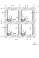
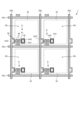
- FIG. 5 is a plan view showing the detection device according to the first embodiment.
- FIG. 6 is a plan view schematically showing the detection device according to the first embodiment.
- 7 is a plan view schematically showing a first electrode and a transistor of the detection device according to the first embodiment;
- FIG. 8 is a cross-sectional view taken along line VIII-VIII' of FIG.
- FIG. 9 is a cross-sectional view taken along line IX-IX' of FIG.
- FIG. 10 is a plan view showing the detection device according to the second embodiment.
- FIG. 11 is a plan view showing the detection device according to the third embodiment.
- FIG. 1 is a schematic diagram showing a detection device according to the first embodiment.
- the detection device 1 includes a substrate 21, a sensor section 10, a gate line drive circuit 15, a signal line selection circuit 16, a detection circuit 48, a control circuit 122, a power supply circuit 123, It has a first light source substrate 51 , a second light source substrate 52 , a first light source 53 , and a second light source 54 .
- a plurality of first light sources 53 are provided on the first light source substrate 51 .
- a plurality of second light sources 54 are provided on the second light source substrate 52 .
- a control board 121 is electrically connected to the board 21 via a flexible printed board 71 .
- the flexible printed board 71 is, for example, a flexible printed board or a rigid board.
- a detection circuit 48 is provided on the flexible printed circuit board 71 .
- a control circuit 122 and a power supply circuit 123 are provided on the control board 121 .
- the control circuit 122 is, for example, an FPGA (Field Programmable Gate Array).
- the control circuit 122 supplies control signals to the sensor section 10 , the gate line drive circuit 15 and the signal line selection circuit 16 to control the detection operation of the sensor section 10 .
- the control circuit 122 also supplies control signals to the first light source 53 and the second light source 54 to control lighting or non-lighting of the first light source 53 and the second light source 54 .
- the power supply circuit 123 supplies voltage signals such as the sensor power supply signal VDDSNS (see FIG. 4) to the sensor section 10, the gate line drive circuit 15, and the signal line selection circuit 16. FIG. Also, the power supply circuit 123 supplies a power supply voltage to the first light source 53 and the second light source 54 .
- the substrate 21 has a detection area AA and a peripheral area GA.
- the detection area AA is an area in which a plurality of photodiodes PD (see FIG. 4) of the sensor section 10 are provided.
- the peripheral area GA is an area between the outer circumference of the detection area AA and the outer edge of the substrate 21, and is an area in which the plurality of photodiodes PD are not provided.
- the gate line drive circuit 15 and the signal line selection circuit 16 are provided in the peripheral area GA. Specifically, the gate line driving circuit 15 is provided in a region extending along the second direction Dy in the peripheral region GA.
- the signal line selection circuit 16 is provided in an area extending along the first direction Dx in the peripheral area GA, and is provided between the sensor section 10 and the detection circuit 48 .
- the first direction Dx is one direction within a plane parallel to the substrate 21 .
- the second direction Dy is one direction in a plane parallel to the substrate 21 and perpendicular to the first direction Dx. Note that the second direction Dy may cross the first direction Dx instead of being perpendicular to it.
- plane view refers to the positional relationship when viewed from a direction perpendicular to the substrate 21 .
- the plurality of first light sources 53 are provided on the first light source substrate 51 and arranged along the second direction Dy.
- a plurality of second light sources 54 are provided on the second light source substrate 52 and arranged along the second direction Dy.
- the first light source base material 51 and the second light source base material 52 are electrically connected to a control circuit 122 and a power supply circuit 123 via terminal portions 124 and 125 provided on the control board 121, respectively.
- first light sources 53 and the plurality of second light sources 54 for example, inorganic LEDs (Light Emitting Diodes) or organic ELs (OLEDs: Organic Light Emitting Diodes) are used.
- the plurality of first light sources 53 and the plurality of second light sources 54 emit first light and second light with different wavelengths, respectively.
- the first light emitted from the first light source 53 is mainly reflected by the surface of the object to be detected such as a finger and enters the sensor section 10 .
- the sensor unit 10 can detect a fingerprint by detecting the uneven shape of the surface of the finger or the like.
- the second light emitted from the second light source 54 is mainly reflected inside the finger or the like or transmitted through the finger or the like and enters the sensor section 10 .
- the sensor unit 10 can detect information about the internal living body such as a finger.
- the biological information includes, for example, finger and palm pulse waves, pulse, blood vessel images, and the like. That is, the detection device 1 may be configured as a fingerprint detection device that detects fingerprints or a vein detection device that detects blood vessel patterns such as veins.
- the first light may have a wavelength of 500 nm or more and 600 nm or less, for example about 550 nm
- the second light may have a wavelength of 780 nm or more and 950 nm or less, for example about 850 nm.
- the first light is blue or green visible light
- the second light is infrared light.
- the sensor unit 10 can detect a fingerprint based on the first light emitted from the first light source 53 .
- the second light emitted from the second light source 54 is reflected inside an object to be detected such as a finger or is transmitted/absorbed by the finger or the like and enters the sensor section 10 .
- the sensor unit 10 can detect a pulse wave and a blood vessel image (blood vessel pattern) as information about the internal living body of a finger or the like.
- the first light may have a wavelength of 600 nm or more and 700 nm or less, for example about 660 nm
- the second light may have a wavelength of 780 nm or more and 900 nm or less, for example about 850 nm.
- the sensor unit 10 obtains information about the living body in addition to the pulse wave, the pulse, and the blood vessel image. , can detect blood oxygen saturation.
- the detection device 1 since the detection device 1 has the first light source 53 and the plurality of second light sources 54, by performing detection based on the first light and detection based on the second light, various can detect information about the living body of
- the detection device 1 is provided with a plurality of types of light sources (first light source 53 and second light source 54) as light sources.
- first light source 53 and second light source 54 may be arranged on each of the first light source substrate 51 and the second light source substrate 52 .
- the number of light source substrates provided with the first light source 53 and the second light source 54 may be one or three or more.
- at least one light source may be arranged.
- FIG. 2 is a block diagram showing a configuration example of the detection device according to the first embodiment.
- the detection device 1 further has a detection control section 11 and a detection section 40 .
- a part or all of the functions of the detection control section 11 are included in the control circuit 122 .
- part or all of the functions of the detection unit 40 other than the detection circuit 48 are included in the control circuit 122 .
- the sensor unit 10 has a plurality of photodiodes PD.
- the photodiode PD included in the sensor unit 10 outputs an electrical signal corresponding to the irradiated light to the signal line selection circuit 16 as the detection signal Vdet. Further, the sensor section 10 performs detection according to the gate drive signal Vgcl supplied from the gate line drive circuit 15 .
- the detection control unit 11 is a circuit that supplies control signals to the gate line drive circuit 15, the signal line selection circuit 16, and the detection unit 40, respectively, and controls their operations.
- the detection control unit 11 supplies various control signals such as a start signal STV, a clock signal CK, and a reset signal RST1 to the gate line drive circuit 15 .
- the detection control unit 11 also supplies various control signals such as the selection signal ASW to the signal line selection circuit 16 .
- the detection control unit 11 also supplies various control signals to the first light source 53 and the second light source 54 to control lighting and non-lighting of each.
- the gate line drive circuit 15 is a circuit that drives a plurality of gate lines GCL (see FIG. 3) based on various control signals.
- the gate line driving circuit 15 sequentially or simultaneously selects a plurality of gate lines GCL and supplies a gate driving signal Vgcl to the selected gate lines GCL. Thereby, the gate line drive circuit 15 selects a plurality of photodiodes PD connected to the gate line GCL.
- the signal line selection circuit 16 is a switch circuit that sequentially or simultaneously selects a plurality of signal lines SGL (see FIG. 3).
- the signal line selection circuit 16 is, for example, a multiplexer.
- the signal line selection circuit 16 connects the selected signal line SGL and the detection circuit 48 based on the selection signal ASW supplied from the detection control section 11 . Thereby, the signal line selection circuit 16 outputs the detection signal Vdet of the photodiode PD to the detection section 40 .
- the detection unit 40 includes a detection circuit 48 , a signal processing circuit 44 , a coordinate extraction circuit 45 , a storage circuit 46 , a detection timing control circuit 47 , an image processing circuit 49 and an output processing unit 50 .
- the detection timing control circuit 47 operates in synchronization with the detection circuit 48, the signal processing circuit 44, the coordinate extraction circuit 45, and the image processing circuit 49 based on the control signal supplied from the detection control section 11. to control.
- the detection circuit 48 is, for example, an analog front end circuit (AFE, Analog Front End).
- the detection circuit 48 is a signal processing circuit having at least the functions of the detection signal amplification circuit 42 and the A/D conversion circuit 43 .
- the detection signal amplifier circuit 42 amplifies the detection signal Vdet.
- the A/D conversion circuit 43 converts the analog signal output from the detection signal amplification circuit 42 into a digital signal.
- the signal processing circuit 44 is a logic circuit that detects a predetermined physical quantity input to the sensor section 10 based on the output signal of the detection circuit 48 .
- the signal processing circuit 44 can detect the unevenness of the surface of the finger or palm based on the signal from the detection circuit 48 when the finger touches or approaches the detection surface.
- the signal processing circuit 44 can detect information about the living body based on the signal from the detection circuit 48 .
- the biological information includes, for example, finger and palm blood vessel images, pulse waves, pulse, blood oxygen concentration, and the like.
- the signal processing circuit 44 may acquire the detection signals Vdet (information related to the living body) simultaneously detected by the plurality of photodiodes PD, and perform a process of averaging them.
- the detection unit 40 suppresses measurement errors caused by noise and relative positional deviation between the object to be detected such as a finger and the sensor unit 10, thereby enabling stable detection.
- the storage circuit 46 temporarily stores the signal calculated by the signal processing circuit 44 .
- the storage circuit 46 may be, for example, a RAM (Random Access Memory), a register circuit, or the like.
- the coordinate extraction circuit 45 is a logic circuit that obtains the detected coordinates of the unevenness of the surface of the finger or the like when the signal processing circuit 44 detects contact or proximity of the finger.
- a coordinate extraction circuit 45 is a logic circuit for obtaining the detected coordinates of the blood vessels of the fingers and palms.
- the image processing circuit 49 combines the detection signals Vdet output from the photodiodes PD of the sensor unit 10 to obtain two-dimensional information representing the shape of the uneven surface of the finger or the like and two-dimensional information representing the shape of the blood vessels of the finger or palm. Generate information.
- the coordinate extraction circuit 45 may output the detection signal Vdet as the sensor output voltage Vo without calculating the detection coordinates.
- the coordinate extraction circuit 45 and the image processing circuit 49 may not be included in the detection unit 40 .
- the output processing unit 50 functions as a processing unit that performs processing based on outputs from the multiple photodiodes PD.
- the output processing unit 50 may include the detected coordinates obtained by the coordinate extraction circuit 45, the two-dimensional information generated by the image processing circuit 49, and the like in the sensor output voltage Vo. Also, the function of the output processing unit 50 may be integrated into another configuration (for example, the image processing circuit 49 or the like).
- FIG. 3 is a circuit diagram showing the detection device.
- the sensor section 10 has a plurality of detection elements PAA arranged in a matrix.
- a photodiode PD is provided for each of the plurality of detection elements PAA.
- the gate line GCL extends in the first direction Dx and is connected to a plurality of detection elements PAA arranged in the first direction Dx.
- the signal line SGL extends in the second direction Dy and is connected to the photodiodes PD of the plurality of detection elements PAA arranged in the second direction Dy.
- the resolution of the sensor is, for example, 508 dpi (dots per inch), and the number of cells is 252 ⁇ 256.
- the sensor section 10 is provided between the signal line selection circuit 16 and the reset circuit 17 . Not limited to this, the signal line selection circuit 16 and the reset circuit 17 may be connected to the ends of the signal line SGL in the same direction.
- the gate line drive circuit 15 receives various control signals such as the start signal STV, the clock signal CK, and the reset signal RST1 from the control circuit 122 (see FIG. 1).
- the gate line drive circuit 15 sequentially selects a plurality of gate lines GCL(1), GCL(2), .
- the gate line drive circuit 15 supplies a gate drive signal Vgcl to the selected gate line GCL.
- the gate drive signal Vgcl is supplied to the plurality of first switching elements Tr connected to the gate line GCL, and the plurality of detection elements PAA arranged in the first direction Dx are selected as detection targets.
- the signal line selection circuit 16 has multiple selection signal lines Lsel, multiple output signal lines Lout, and a third switching element TrS.
- the plurality of third switching elements TrS are provided corresponding to the plurality of signal lines SGL, respectively.
- Six signal lines SGL(1), SGL(2), . . . , SGL(6) are connected to a common output signal line Lout1.
- Six signal lines SGL(7), SGL(8), . . . , SGL(12) are connected to a common output signal line Lout2.
- the output signal lines Lout1 and Lout2 are connected to the detection circuit 48, respectively.
- the signal lines SGL(1), SGL(2), . Signal line block A plurality of selection signal lines Lsel are connected to the gates of the third switching elements TrS included in one signal line block. Also, one selection signal line Lsel is connected to the gates of the third switching elements TrS of the plurality of signal line blocks.
- the control circuit 122 (see FIG. 1) sequentially supplies the selection signal ASW to the selection signal line Lsel.
- the signal line selection circuit 16 sequentially selects the signal lines SGL in one signal line block in a time division manner by the operation of the third switching element TrS. Also, the signal line selection circuit 16 selects one signal line SGL in each of the plurality of signal line blocks.
- the detection device 1 can reduce the number of ICs (Integrated Circuits) including the detection circuit 48 or the number of IC terminals.
- the signal line selection circuit 16 may bundle a plurality of signal lines SGL and connect them to the detection circuit 48 .
- the reset circuit 17 has a reference signal line Lvr, a reset signal line Lrst and a fourth switching element TrR.
- the fourth switching elements TrR are provided corresponding to the plurality of signal lines SGL.
- the reference signal line Lvr is connected to one of the sources or drains of the plurality of fourth switching elements TrR.
- the reset signal line Lrst is connected to gates of the plurality of fourth switching elements TrR.
- the control circuit 122 supplies the reset signal RST2 to the reset signal line Lrst.
- the multiple fourth switching elements TrR are turned on, and the multiple signal lines SGL are electrically connected to the reference signal line Lvr.
- the power supply circuit 123 supplies the reference signal COM to the reference signal line Lvr.
- the reference signal COM is supplied to the capacitive elements Ca (see FIG. 4) included in the plurality of detection elements PAA.
- FIG. 4 is a circuit diagram showing a plurality of detection elements. 4 also shows the circuit configuration of the detection circuit 48.
- the detection element PAA includes a photodiode PD, a capacitive element Ca, and a first switching element Tr.
- the capacitive element Ca is a capacitance (sensor capacitance) formed in the photodiode PD and equivalently connected in parallel with the photodiode PD.
- FIG. 4 shows two gate lines GCL(m) and GCL(m+1) aligned in the second direction Dy among the plurality of gate lines GCL. Also, two signal lines SGL(n) and SGL(n+1) arranged in the first direction Dx among the plurality of signal lines SGL are shown.
- the detection element PAA is an area surrounded by the gate line GCL and the signal line SGL.
- the first switching element Tr is provided corresponding to the photodiode PD.
- the first switching element Tr is configured by a thin film transistor, and in this example, is configured by an n-channel MOS (Metal Oxide Semiconductor) type TFT (Thin Film Transistor).
- MOS Metal Oxide Semiconductor
- TFT Thin Film Transistor
- the gates of the first switching elements Tr belonging to the plurality of detection elements PAA arranged in the first direction Dx are connected to the gate line GCL.
- the sources of the first switching elements Tr belonging to the plurality of detection elements PAA arranged in the second direction Dy are connected to the signal line SGL.
- the drain of the first switching element Tr is connected to the cathode of the photodiode PD and the capacitive element Ca.
- a sensor power supply signal VDDSNS is supplied from the power supply circuit 123 to the anode of the photodiode PD.
- a reference signal COM which is the initial potential of the signal line SGL and the capacitor Ca, is supplied from the power supply circuit 123 to the signal line SGL and the capacitor Ca.
- the detection device 1 can detect a signal corresponding to the amount of light irradiated to the photodiode PD for each detection element PAA or for each block unit PAG.
- the detection circuit 48 is connected to the signal line SGL with the switch SSW turned on during the readout period.
- the detection signal amplifier circuit 42 of the detection circuit 48 converts the current fluctuation supplied from the signal line SGL into a voltage fluctuation and amplifies it.
- a reference potential (Vref) having a fixed potential is input to the non-inverting input (+) of the detection signal amplifier circuit 42, and the signal line SGL is connected to the inverting input terminal (-).
- the same signal as the reference signal COM is input as the reference potential (Vref) voltage.
- the signal processing circuit 44 calculates the difference between the detection signal Vdet when light is irradiated and the detection signal Vdet when light is not irradiated as the sensor output voltage Vo.
- the detection signal amplifier circuit 42 has a capacitive element Cb and a reset switch RSW. During the reset period, the reset switch RSW is turned on to reset the charge of the capacitive element Cb.
- FIG. 5 is a plan view showing the detection device according to the first embodiment.
- FIG. 6 is a plan view schematically showing the detection device according to the first embodiment.
- 7 is a plan view schematically showing a first electrode and a transistor of the detection device according to the first embodiment; FIG. In FIG. 6, the insulating film 95 is hatched for easy viewing of the drawing.
- FIG. 7 is a plan view schematically showing a portion of the detection device excluding the insulating film of FIG.
- a control board 121 is electrically connected to the board 21 via a flexible printed board 71 .
- a detection circuit 48 is provided on the flexible printed circuit board 71 .
- a control circuit 122 and a power supply circuit 123 are provided on the control board 121 .
- the control circuit 122 is, for example, an FPGA (Field Programmable Gate Array).
- the control circuit 122 supplies control signals to the sensor section 10 , the gate line drive circuit 15 and the signal line selection circuit 16 to control the detection operation of the sensor section 10 .
- the power supply circuit 123 supplies voltage signals such as the sensor power supply signal VDDSNS (see FIG. 4) to the sensor section 10, the gate line drive circuit 15, and the signal line selection circuit 16.
- the substrate 21 has a detection area AA and a peripheral area GA.
- the detection area AA is an area including areas overlapping with the plurality of first electrodes 23 of the sensor section 10 .
- the peripheral area GA is an area outside the detection area AA and is an area that does not overlap with the first electrode 23 . That is, the peripheral area GA is an area between the outer circumference of the detection area AA and the edge of the substrate 21 .
- the gate line drive circuit 15 and the signal line selection circuit 16 are provided in the peripheral area GA.
- the plurality of first electrodes 23 are detection electrodes of the photodiodes PD, and output electrical signals according to the light irradiated thereon.
- a plurality of first electrodes 23 of the sensor section 10 are arranged in a matrix in the detection area AA.
- the plurality of first electrodes 23 outputs an electrical signal corresponding to the light irradiated thereon to the signal line selection circuit 16 as the detection signal Vdet.
- the detection device 1 detects information about the living body based on detection signals Vdet from the plurality of first electrodes 23 .
- the photodiode PD functions as a biosensor.
- the plurality of first electrodes 23 performs detection according to the gate drive signal Vgcl supplied from the gate line drive circuit 15 .
- the gate line drive circuit 15 and the signal line selection circuit 16 are provided in the peripheral area GA. Specifically, the gate line driving circuit 15 is provided in a region extending along the second direction Dy in the peripheral region GA.
- the signal line selection circuit 16 is provided in an area extending along the first direction Dx in the peripheral area GA, and is provided between the sensor section 10 and the detection circuit 48 .
- the second electrode 24 covers the detection area AA and has an area larger than the detection area AA.
- a conductive wiring 56 is arranged in the peripheral area GA, and the conductive wiring 56 and the second electrode 24 are electrically connected by a connection terminal 55 .
- the conductive wiring 56 is connected to the power supply circuit 123 shown in FIG. 1, and the sensor power supply signal VDDSNS is supplied to the conductive wiring 56 .
- the photodiode PD, the first electrode 23 and the first switching element Tr are provided in a region surrounded by the gate line GCL and the signal line SGL.
- the first electrode 23 is a lower electrode (cathode electrode) of the photodiode PD, and the plurality of photodiodes PD and the plurality of first electrodes 23 are arranged in a matrix above the substrate 21 .
- the insulating film 95 is provided between the adjacent first electrodes 23 and covers the outer periphery of the first electrodes 23 . More specifically, the insulating film 95 includes a first portion 95a extending in the first direction Dx and a second portion 95b extending in the second direction Dy. The insulating film 95 is provided in a grid pattern by intersecting the plurality of first portions 95a and the plurality of second portions 95b.
- the first portion 95a is provided so as to overlap with the gate line GCL, and is provided between the first electrodes 23 adjacent in the second direction Dy with the gate line GCL interposed therebetween.
- the second portion 95b is provided so as to overlap the signal line SGL, and is provided between the first electrodes 23 adjacent in the first direction Dx with the signal line SGL interposed therebetween.
- the multiple first electrodes 23 are partitioned by the insulating film 95 .
- the plurality of first electrodes 23 are connected to the lower buffer layer 32 (see FIG. 8) of the photodiode PD through openings OP formed in the insulating film 95 .
- the lower buffer layer 32 is an electron transport layer.
- the first switching element Tr has a semiconductor layer 61, a source electrode 62, a drain electrode 63 and a gate electrode 64.
- the semiconductor layer 61 extends along the gate line GCL and is provided to cross the gate electrode 64 in plan view.
- Gate electrode 64 is connected to gate line GCL and extends in a direction orthogonal to gate line GCL.
- One end side of the semiconductor layer 61 is connected to the source electrode 62 via the second contact hole CH2.
- the first electrode 23 is electrically connected to the source electrode 62 of the first switching element Tr through the first contact hole CH1. Thereby, the first switching element Tr is electrically connected to the photodiode PD.
- the other end side of the semiconductor layer 61 is connected to the drain electrode 63 through the third contact hole CH3. Drain electrode 63 is connected to signal line SGL.
- the second organic insulating film 96 is provided to cover the first contact hole CH1.
- Detailed configurations of the second organic insulating film 96 and the photodiode PD will be described with reference to FIG.
- the configuration and arrangement of the first switching element Tr shown in FIGS. 6 and 7 are merely examples, and can be changed as appropriate.
- FIG. 8 is a cross-sectional view taken along line VIII-VIII' of FIG.
- the detection device 1 includes a substrate 21, a first switching element Tr, a first organic insulating film 94, a first electrode 23, an insulating film 95, a second organic insulating film 96, It has an organic photodiode layer PDL, a second electrode 24 , sealing films 97 a , 97 b , 97 c and a resin mask 98 .
- the substrate 21 is an insulating base material, for example, glass or resin material is used.
- the substrate 21 is not limited to a flat plate shape, and may have a curved surface. In this case, the substrate 21 may be a film-like resin.
- the direction from the substrate 21 toward the organic photodiode layer PDL in the direction perpendicular to the surface of the substrate 21 is referred to as “upper” or simply “upper”. Also, the direction from the organic photodiode layer PDL to the substrate 21 is referred to as “lower side” or simply “lower side.”
- the light shielding film 65 is provided on the substrate 21 .
- a light shielding film 65 is provided between the semiconductor layer 61 and the substrate 21 .
- the light shielding film 65 can prevent light from entering the channel region of the semiconductor layer 61 from the substrate 21 side.
- the undercoat film 91 is provided on the substrate 21 covering the light shielding film 65 .
- the undercoat film 91 is made of, for example, an inorganic insulating film such as a silicon nitride film or a silicon oxide film.
- the structure of the undercoat film 91 is not limited to a single layer film, and may be a laminated film in which a plurality of inorganic insulating films are laminated.
- An undercoat film may also be provided between the substrate 21 and the light shielding film 65 .
- a plurality of first switching elements Tr are provided on the substrate 21 .
- the semiconductor layer 61 is provided on the undercoat film 91 .
- Polysilicon for example, is used for the semiconductor layer 61 .
- the semiconductor layer 61 is not limited to this, and may be a microcrystalline oxide semiconductor, an amorphous oxide semiconductor, a low-temperature polysilicon, or the like. Although only an n-type TFT is shown as the first switching element Tr, a p-type TFT may be formed at the same time.
- the gate insulating film 92 is provided on the undercoat film 91 to cover the semiconductor layer 61 .
- the gate insulating film 92 is, for example, an inorganic insulating film such as a silicon oxide film.
- Gate electrode 64 is provided on gate insulating film 92 .
- the first switching element Tr has a top gate structure.
- the first switching element Tr may have a bottom-gate structure or a dual-gate structure in which the gate electrodes 64 are provided on both the upper and lower sides of the semiconductor layer 61 .
- An interlayer insulating film 93 is provided on the gate insulating film 92 to cover the gate electrode 64 .
- the interlayer insulating film 93 has, for example, a laminated structure of a silicon nitride film and a silicon oxide film.
- a source electrode 62 and a drain electrode 63 are provided on the interlayer insulating film 93 .
- the source electrode 62 is connected to the source region of the semiconductor layer 61 through a second contact hole CH2 provided in the gate insulating film 92 and the interlayer insulating film 93.
- the drain electrode 63 is connected to the drain region of the semiconductor layer 61 through a third contact hole CH3 provided in the gate insulating film 92 and the interlayer insulating film 93. As shown in FIG.
- the first organic insulating film 94 is provided on the interlayer insulating film 93 to cover the source electrode 62 and the drain electrode 63 of the first switching element Tr.
- the first organic insulating film 94 is an organic planarizing film, and is superior in wiring step coverage and surface flatness compared to inorganic insulating materials formed by CVD or the like.
- the organic photodiode layer PDL is provided on the first organic insulating film 94 .
- the first electrode 23 and the insulating film 95 are provided between the substrate 21 and the first organic insulating film 94 and the organic photodiode layer PDL in a direction perpendicular to the surface of the substrate 21 .
- the first electrode 23 is provided on the first organic insulating film 94 and is provided to cover the bottom and inner side surfaces of the first contact hole CH1 formed in the first organic insulating film 94.
- the first electrode 23 is connected to the source electrode 62 of the first switching element Tr at the bottom surface of the first contact hole CH1.
- the first electrode 23 is a cathode electrode of the organic photodiode layer PDL, and is formed of, for example, a translucent conductive material such as ITO (Indium Tin Oxide) or IZO (Indium Zinc Oxide).
- the plurality of first electrodes 23 are arranged separately for each detection element PAA (photodiode PD).
- the organic photodiode layer PDL has an area larger than that of the first electrode 23 in plan view, and covers the upper surface of the first electrode 23 and the outer edge portion 23e.
- the insulating film 95 is provided between the adjacent first electrodes 23 and covers the outer edge portion 23 e of the first electrode 23 .
- the insulating film 95 is an inorganic insulating film, and a material such as a silicon nitride film or an aluminum oxide film is used.
- the insulating film 95 has at least one or more openings OP (see FIG. 6) in a region overlapping with the top surface of the first electrode 23 .
- the organic photodiode layer PDL is electrically connected to the first electrode 23 through the opening OP.
- the insulating film 95 is provided between the first organic insulating film 94 and the organic photodiode layer PDL in the region between the adjacent first electrodes 23 . Thereby, the insulating film 95 insulates the adjacent first electrodes 23 . In other words, the insulating film 95 can suppress leakage current between adjacent photodiodes PD.
- the insulating film 95 also functions as a barrier film that suppresses the entry of moisture from the first organic insulating film 94 into the organic photodiode layer PDL in the region between the adjacent first electrodes 23 .
- the second organic insulating film 96 is provided to cover the inside of the first contact hole CH1.
- the first electrode 23 and the second organic insulating film 96 are stacked on the inner and bottom surfaces of the first contact hole CH1.
- a first organic insulating film 94, a first electrode 23, and a second organic insulating film 96 are stacked in this order on the inner surface of the first contact hole CH1.
- On the bottom surface of the first contact hole CH1, the first electrode 23 and the second organic insulating film 96 are stacked in this order on the source electrode 62.
- the second organic insulating film 96 is provided to cover the corner portion 23t of the first electrode 23 at a position overlapping the opening end portion of the first contact hole CH1.
- the organic photodiode layer PDL is provided covering the plurality of first electrodes 23, the insulating film 95 and the second organic insulating film 96. More specifically, the organic photodiode layer PDL includes an active layer 31, a lower buffer layer 32 (first carrier transport layer), and an upper buffer layer 33 (second carrier transport layer). A lower buffer layer 32 (first carrier transport layer) is provided between the active layer 31 and the first electrode 23 . An upper buffer layer 33 (second carrier transport layer) is provided between the active layer 31 and the second electrode 24 . The upper buffer layer 33 is a hole transport layer.
- the lower buffer layer 32 is formed by applying a material such as zinc acetate, ethoxylated polyethyleneimine (PEIE), polyethyleneimine (PEI), or the like.
- the lower buffer layer 32 is a single layer and has a thickness of, for example, about 30 nm or less.
- a mixture of a p-type organic semiconductor and an n-type organic semiconductor is used for the active layer 31 .
- a p-type organic semiconductor for example, PMDPP3T (poly((2,5-bis(2-hexyldecyl)-2,3,5,6-tetrahydro-3,6-dioxopyrrolo(3,4-c)pyrrole-1,4 -diyl)-alt-(3′,3′′-dimethyl-2,2′:5′,2′′-terthiophene)-5,5′′-diyl)).
- examples of n-type organic semiconductors include PC61BM ([6,6]-phenyl C61-butyric acid methyl ester).
- the thickness of the active layer 31 is, for example, about 100 nm or more and 500 nm or less, preferably about 350 nm.
- the upper buffer layer 33 is, for example, a metal oxide layer such as tungsten oxide (WO 3 ) or molybdenum oxide (MoOx).
- the upper buffer layer 33 is formed of a deposited film or a sputtered film, and its thickness is, for example, about 30 nm or less.
- the lower buffer layer 32 , the active layer 31 and the upper buffer layer 33 forming the organic photodiode layer PDL are provided covering the plurality of first electrodes 23 , the insulating film 95 and the second organic insulating film 96 .
- the lower buffer layer 32 is connected to the first electrode 23 in a region overlapping the opening OP of the insulating film 95 .
- the lower buffer layer 32 includes an overlapping portion 32s provided on the insulating film 95 and an overlapping portion 32t provided on the second organic insulating film 96 in a region overlapping with the first contact hole CH1. include.
- the detection device 1 includes a first organic insulating film 94 , a first electrode 23 , a lower buffer layer 32 , an active layer 31 , an upper buffer layer 33 , a second
- the electrodes 24 are stacked in order.
- the first electrode 23, the second organic insulating film 96, the lower buffer layer 32 (overlapping portion 32t), the active layer 31, the upper buffer layer 33, and the second electrode 24 are laminated in this order. be done.
- the first organic insulating film 94, the insulating film 95, the lower buffer layer 32 (overlapping portion 32s), the active layer 31, the upper buffer layer 33, and the second electrode 24 are arranged in this order. Laminated.
- the insulating film 95 is provided between the adjacent first electrodes 23 and covers the outer edges 23e of the first electrodes 23 .
- the thickness of the lower buffer layer 32 is formed thin at the position overlapping with the outer edge portion 23 e of the first electrode 23 .
- the insulating film 95 provides a gap between the active layer 31 and the first electrode 23 . It is possible to suppress the occurrence of short circuits.
- FIG. 8 shows a case where the superimposed portion 32s and the lower buffer layer 32 on the first electrode 23 are formed apart from each other in order to facilitate understanding, but the superimposed portion 32s,
- the lower buffer layer 32 on the first electrode 23 may be formed continuously and integrally.
- the second organic insulating film 96 is provided to cover the inside of the first contact hole CH1, covering the corner 23t of the first electrode 23 formed at the opening end of the first contact hole CH1.
- the region overlapping the first contact hole CH1 is planarized, and the overlapping portion 32t of the lower buffer layer 32 is formed continuously with the lower buffer layer 32 above the first electrode 23.
- the second organic insulating film 96 covers most of the region of the first electrode 23 inside the first contact hole CH1. Therefore, even if part of the lower buffer layer 32 is thinly formed or the lower buffer layer 32 is cut off in the region overlapping with the first contact hole CH1, the second organic insulating film 96 prevents the active layer from being formed. The occurrence of a short circuit between 31 and first electrode 23 can be suppressed.
- the organic insulating film 96 extends over the region overlapping with the first contact hole CH1 and the region not overlapping with the first contact hole CH1. Variations in film thickness of the active layer 31, the lower buffer layer 32, and the upper buffer layer 33 that form the photodiode layer PDL are suppressed. That is, compared to the configuration in which the second organic insulating film 96 is not provided, the active layer 31, the lower buffer layer 32, and the upper buffer layer 33 are not cut or thinned in the region overlapping the first contact hole CH1. Suppressed. Thereby, the detection device 1 can suppress leakage current between the anode and the cathode of the photodiode PD.
- the second electrode 24 is an upper electrode provided on the organic photodiode layer PDL. More specifically, the second electrode 24 is provided on the upper buffer layer 33 of the organic photodiode layer PDL.
- the second electrode 24 is an anode electrode of the photodiode PD, and is formed continuously over the plurality of detection elements PAA (photodiodes PD).
- the second electrode 24 is made of a metal material such as silver (Ag), and functions as a reflective electrode.
- the second electrode 24 is not limited to this, and the second electrode 24 may be made of a conductive material having translucency like the first electrode 23 .
- the sealing films 97 a , 97 b , 97 c are provided on the second electrode 24 .
- an inorganic insulating film such as a silicon nitride film or an aluminum oxide film is used.
- a resin film such as acrylic is used.
- the sealing films 97a, 97b, and 97c are not limited to laminated films in which an inorganic insulating film and an organic insulating film are laminated, and may be a single layer.
- a resin mask 98 is provided covering the sealing film 97c.
- the organic photodiode layer PDL is well sealed by the sealing films 97a, 97b, and 97c and the resin mask 98, and it is possible to suppress penetration of moisture from the upper surface side.
- the thickness of the first electrode 23 is, for example, about 50 nm.
- the thickness of the second electrode 24 is, for example, about 100 nm or less. That is, the lower buffer layer 32 and the upper buffer layer 33 are each thinner than the active layer 31 and thinner than the first electrode 23 and the second electrode 24 . In other words, the thickness of each of the first electrode 23 and the second electrode 24 is thinner than the active layer 31 and thicker than the lower buffer layer 32 and the upper buffer layer 33 .
- the materials and manufacturing methods of the lower buffer layer 32, the active layer 31, and the upper buffer layer 33 are merely examples, and other materials and manufacturing methods may be used.
- the lower buffer layer 32 may be a deposited film or sputtered film using materials such as zinc oxide (ZnO) and titanium oxide (TiO 2 ).
- the upper buffer layer 33 may be a deposited film or sputtered film using a material such as nickel oxide (NiO), or the upper buffer layer 33 may be vanadium oxide (V 2 O 5 ) or tungsten oxide ( WO 3 ) or the like, or a material such as PEDOT:PSS, may be used for coating.
- planar shape and cross-sectional shape of the insulating film 95 and the second organic insulating film 96 shown in FIGS. 6 and 8 are only schematic, and can be changed as appropriate.
- the upper surface of the second organic insulating film 96 is not limited to a configuration having a curved surface, and a portion of the upper surface may be formed flat.
- the planar shape of the second organic insulating film 96 is not limited to a square shape, and may be other shapes such as a circular shape, a polygonal shape, etc. according to the planar shape of the first contact hole CH1.
- the opening OP formed in the insulating film 95 is not limited to a rectangular shape, and can be changed as appropriate according to the shape of the first electrode 23 .
- FIG. 9 is a cross-sectional view taken along line IX-IX' of FIG.
- the second electrodes 24 connect to conductive traces 56 in a peripheral area GA around the sensing area AA.
- the organic photodiode layer PDL has a non-formation region in the peripheral region GA, and the side surface 33e of the upper buffer layer 33, the side surface 31e of the active layer 31, and the side surface 32e of the lower buffer layer 32 are exposed at the ends.
- the side surface 33e of the upper buffer layer 33, the side surface 31e of the active layer 31, and the side surface 32e of the lower buffer layer 32 are the side surface PDLe of the organic photodiode layer PDL.
- the second electrode 24 provided covering the side surface PDLe of the organic photodiode layer PDL is electrically connected to the side surface 33 e of the upper buffer layer 33 , the side surface 31 e of the active layer 31 and the side surface 32 e of the lower buffer layer 32 . Therefore, the second electrode 24 is laminated on the exposed side surface PDLe of the organic photodiode layer PDL in the peripheral region GA, and a leakage current may flow between the second electrode 24 and the outermost first electrode 23.
- a third electrode is provided between the second electrode 24 on the side surface PDLe of the organic photodiode layer PDL and the outermost first electrode 23. 25 are formed.
- connection terminals 55 are formed in the peripheral area GA. Conductive wiring 56 is formed on undercoat film 91 .
- the connection terminal 55 has a conductive pedestal portion 57 electrically connected to the conductive wiring 56, and a terminal electrode 23a electrically connected to the pedestal portion 57 via the contact hole CHA.
- a second organic insulating film 96 is provided to cover the inside of the contact hole CHA.
- the terminal electrode 23 a is electrically connected to the second electrode 24 .
- the third electrode 25 is electrically connected to the reference potential wiring 26 via the contact hole CHC.
- the reference potential wiring 26 is routed along the outermost circumference of the first electrode 23 .
- the third electrode 25 has the same potential as the reference signal, which is the reset potential supplied from the reset circuit 17 to the signal line SGL. As a result, the potential difference between the third electrode 25 and the first electrode 23 is reduced, and a leak current from the third electrode 25 to the first electrode 23 is less likely to occur.
- leakage current from the second electrode 24 to the third electrode 25 becomes a problem during a period in which light detection is not performed, the same potential as that of the second electrode 24 is supplied to the reference potential wiring 26 . can be As a result, the potential difference between the third electrode 25 and the second electrode 24 is reduced, and a leak current from the second electrode 24 to the third electrode 25 is less likely to occur.
- the second organic insulating film 96 is provided to cover the inside of the contact hole CHC.
- the third electrode 25 is routed along the outermost periphery of the first electrode 23 and surrounds the first electrode 23 in a square shape. Thus, the third electrode 25 surrounds the entire outermost periphery of the first electrode 23 .
- the second electrode 24 is electrically connected to a conductive wiring 56 drawn around the peripheral area GA outside the third electrode 25 .
- the detection device 1 of the first embodiment includes a plurality of photodiodes PD provided on the substrate 21, a plurality of first electrodes 23, a second electrode 24, a third electrode 25, and an organic photodiode PD.
- a diode layer PDL is provided.
- the plurality of first electrodes 23 are provided corresponding to each of the plurality of photodiodes PD.
- the second electrode 24 is provided across the plurality of photodiodes PD.
- the organic photodiode layer PDL includes a lower buffer layer 32 (first carrier transport layer), an active layer 31 and an upper buffer layer 33 (second carrier transport layer), and is provided across a plurality of photodiodes PD.
- the plurality of photodiodes PD includes the first electrode 23, the lower buffer layer 32 (first carrier transport layer), the active layer 31 and the upper buffer layer 33 (second carrier transport layer). layer), and the second electrode 24 are stacked in this order.
- a reference potential is supplied to the third electrode 25 .
- the third electrode 25 is arranged between the second electrode 24 provided to cover the side surface PDLe of the organic photodiode layer PDL outside the detection area AA and the first electrode 23 arranged on the outermost periphery. .
- FIG. 10 is a plan view showing the detection device according to the second embodiment.
- the same reference numerals are assigned to the same components as those described in the above-described embodiment, and overlapping descriptions will be omitted.
- the conductive wiring 56 is arranged in a U-shape in the peripheral area GA, and the conductive wiring 56 and the second It is electrically connected to the electrode 24 .
- the conductive wiring 56 is connected to the power supply circuit 123 shown in FIG. 1, and the sensor power supply signal VDDSNS is supplied to the conductive wiring 56 .
- the third electrode 25 is routed along the outermost periphery of the first electrode 23 and surrounds the first electrode 23 in a U-shape.
- the third electrode 25 is arranged except for one side of the sides surrounding the outermost periphery of the first electrode 23 .
- the second electrode 24 is arranged inside the side surface PDLe of the organic photodiode layer PDL. That is, in the region where the third electrode 25 is not arranged, the second electrode 24 is not laminated on the side surface PDLe of the organic photodiode layer PDL. This suppresses leakage current in the region where the third electrode 25 is not arranged.
- FIG. 11 is a plan view showing the detection device according to the third embodiment.
- the same reference numerals are assigned to the same components as those described in the above-described embodiment, and overlapping descriptions will be omitted.
- the conductive wiring 56 is linearly arranged in a part of the peripheral area GA, and the conductive wiring 56 is connected to the connection terminal 55. It is electrically connected to the second electrode 24 .
- the conductive wiring 56 is connected to the power supply circuit 123 shown in FIG. 1, and the sensor power supply signal VDDSNS is supplied to the conductive wiring 56 .
- the third electrode 25 is routed along the outermost periphery of the first electrode 23 and arranged in a straight line.
- the third electrode 25 is arranged only on one side of the sides surrounding the outermost periphery of the first electrode 23 .
- the second electrode 24 is arranged inside the side surface PDLe of the organic photodiode layer PDL. That is, in the region where the third electrode 25 is not arranged, the second electrode 24 is not laminated on the side surface PDLe of the organic photodiode layer PDL. This suppresses leakage current in the regions of the plurality of sides where the third electrode 25 is not arranged.
Landscapes
- Engineering & Computer Science (AREA)
- General Physics & Mathematics (AREA)
- Physics & Mathematics (AREA)
- Multimedia (AREA)
- Human Computer Interaction (AREA)
- Theoretical Computer Science (AREA)
- Vascular Medicine (AREA)
- General Health & Medical Sciences (AREA)
- Health & Medical Sciences (AREA)
- Spectroscopy & Molecular Physics (AREA)
- Signal Processing (AREA)
- Solid State Image Pick-Up Elements (AREA)
- Transforming Light Signals Into Electric Signals (AREA)
Priority Applications (4)
| Application Number | Priority Date | Filing Date | Title |
|---|---|---|---|
| CN202380021037.XA CN118661262A (zh) | 2022-02-09 | 2023-01-31 | 检测装置 |
| JP2023580180A JP7774649B2 (ja) | 2022-02-09 | 2023-01-31 | 検出装置 |
| US18/791,685 US20240393173A1 (en) | 2022-02-09 | 2024-08-01 | Detection device |
| JP2025189040A JP2026020189A (ja) | 2022-02-09 | 2025-11-10 | 電子機器 |
Applications Claiming Priority (2)
| Application Number | Priority Date | Filing Date | Title |
|---|---|---|---|
| JP2022018801 | 2022-02-09 | ||
| JP2022-018801 | 2022-02-09 |
Related Child Applications (1)
| Application Number | Title | Priority Date | Filing Date |
|---|---|---|---|
| US18/791,685 Continuation US20240393173A1 (en) | 2022-02-09 | 2024-08-01 | Detection device |
Publications (1)
| Publication Number | Publication Date |
|---|---|
| WO2023153262A1 true WO2023153262A1 (ja) | 2023-08-17 |
Family
ID=87564229
Family Applications (1)
| Application Number | Title | Priority Date | Filing Date |
|---|---|---|---|
| PCT/JP2023/002953 Ceased WO2023153262A1 (ja) | 2022-02-09 | 2023-01-31 | 検出装置 |
Country Status (4)
| Country | Link |
|---|---|
| US (1) | US20240393173A1 (https=) |
| JP (2) | JP7774649B2 (https=) |
| CN (1) | CN118661262A (https=) |
| WO (1) | WO2023153262A1 (https=) |
Cited By (1)
| Publication number | Priority date | Publication date | Assignee | Title |
|---|---|---|---|---|
| WO2026009704A1 (ja) * | 2024-07-04 | 2026-01-08 | 株式会社ジャパンディスプレイ | 検出装置及び検出装置の製造方法 |
Citations (4)
| Publication number | Priority date | Publication date | Assignee | Title |
|---|---|---|---|---|
| JP2005057281A (ja) * | 2003-08-01 | 2005-03-03 | Ge Medical Systems Global Technology Co Llc | フォト・エレクトロン直接変換検出器アレイ用のガードリング |
| JP2007319199A (ja) * | 2006-05-30 | 2007-12-13 | Hitachi Ltd | 放射線検出器、及びこれを搭載した放射線撮像装置 |
| WO2012056949A1 (ja) * | 2010-10-26 | 2012-05-03 | 富士フイルム株式会社 | 放射線画像撮影装置 |
| JP2019121804A (ja) * | 2018-01-10 | 2019-07-22 | パナソニックIpマネジメント株式会社 | イメージセンサ |
Family Cites Families (15)
| Publication number | Priority date | Publication date | Assignee | Title |
|---|---|---|---|---|
| JPH03212975A (ja) * | 1990-01-17 | 1991-09-18 | Fuji Xerox Co Ltd | イメージセンサ |
| JP2669919B2 (ja) * | 1990-03-07 | 1997-10-29 | 三洋電機株式会社 | 光電変換素子の製造方法 |
| JP3059514B2 (ja) * | 1991-03-18 | 2000-07-04 | 株式会社半導体エネルギー研究所 | 光電変換装置ならびにイメージセンサおよびそれらの作製方法 |
| JP3732244B2 (ja) * | 1994-09-30 | 2006-01-05 | 株式会社島津製作所 | X線撮像装置 |
| DE19926582A1 (de) | 1999-06-11 | 2000-12-14 | Philips Corp Intellectual Pty | Sensor |
| US6724010B1 (en) | 2000-08-03 | 2004-04-20 | General Electric Company | Solid state imager having gated photodiodes and method for making same |
| JP5235348B2 (ja) | 2007-07-26 | 2013-07-10 | 富士フイルム株式会社 | 放射線撮像素子 |
| JP2010210590A (ja) | 2009-03-12 | 2010-09-24 | Fujifilm Corp | 放射線検出器 |
| JP5728451B2 (ja) | 2012-09-19 | 2015-06-03 | 富士フイルム株式会社 | 有機固体撮像素子およびその製造方法 |
| JP6233717B2 (ja) | 2012-12-28 | 2017-11-22 | パナソニックIpマネジメント株式会社 | 固体撮像装置およびその製造方法 |
| JP2015012239A (ja) | 2013-07-01 | 2015-01-19 | ソニー株式会社 | 撮像素子および電子機器 |
| JP6138639B2 (ja) | 2013-09-12 | 2017-05-31 | ソニーセミコンダクタソリューションズ株式会社 | 固体撮像素子および製造方法、並びに電子機器 |
| JP7162275B2 (ja) | 2018-06-14 | 2022-10-28 | パナソニックIpマネジメント株式会社 | 制御電極と、透明電極と、前記制御電極と前記透明電極の側面とを電気的に接続する接続層と、を備えるイメージセンサ |
| JP7692310B2 (ja) * | 2021-08-23 | 2025-06-13 | 株式会社ジャパンディスプレイ | 検出装置 |
| JP2023136697A (ja) * | 2022-03-17 | 2023-09-29 | 株式会社ジャパンディスプレイ | 有機フォトダイオードデバイス |
-
2023
- 2023-01-31 CN CN202380021037.XA patent/CN118661262A/zh active Pending
- 2023-01-31 JP JP2023580180A patent/JP7774649B2/ja active Active
- 2023-01-31 WO PCT/JP2023/002953 patent/WO2023153262A1/ja not_active Ceased
-
2024
- 2024-08-01 US US18/791,685 patent/US20240393173A1/en active Pending
-
2025
- 2025-11-10 JP JP2025189040A patent/JP2026020189A/ja active Pending
Patent Citations (4)
| Publication number | Priority date | Publication date | Assignee | Title |
|---|---|---|---|---|
| JP2005057281A (ja) * | 2003-08-01 | 2005-03-03 | Ge Medical Systems Global Technology Co Llc | フォト・エレクトロン直接変換検出器アレイ用のガードリング |
| JP2007319199A (ja) * | 2006-05-30 | 2007-12-13 | Hitachi Ltd | 放射線検出器、及びこれを搭載した放射線撮像装置 |
| WO2012056949A1 (ja) * | 2010-10-26 | 2012-05-03 | 富士フイルム株式会社 | 放射線画像撮影装置 |
| JP2019121804A (ja) * | 2018-01-10 | 2019-07-22 | パナソニックIpマネジメント株式会社 | イメージセンサ |
Cited By (1)
| Publication number | Priority date | Publication date | Assignee | Title |
|---|---|---|---|---|
| WO2026009704A1 (ja) * | 2024-07-04 | 2026-01-08 | 株式会社ジャパンディスプレイ | 検出装置及び検出装置の製造方法 |
Also Published As
| Publication number | Publication date |
|---|---|
| CN118661262A (zh) | 2024-09-17 |
| JP7774649B2 (ja) | 2025-11-21 |
| US20240393173A1 (en) | 2024-11-28 |
| JPWO2023153262A1 (https=) | 2023-08-17 |
| JP2026020189A (ja) | 2026-02-06 |
Similar Documents
| Publication | Publication Date | Title |
|---|---|---|
| JP7751416B2 (ja) | 検出装置 | |
| JP7633109B2 (ja) | 検出装置 | |
| JP7818127B2 (ja) | 検出装置 | |
| US12514092B2 (en) | Detection device and imaging device | |
| JP2026020189A (ja) | 電子機器 | |
| JP7606941B2 (ja) | 検出装置 | |
| JP7684887B2 (ja) | 検出装置 | |
| JP2024136770A (ja) | 検出装置 | |
| JP2022190538A (ja) | 検出装置 | |
| US12396102B2 (en) | Electronic device | |
| WO2024135561A1 (ja) | 検出装置 | |
| WO2024185478A1 (ja) | 検出装置 | |
| WO2026048984A1 (ja) | 検出装置 | |
| WO2025022960A1 (ja) | 検出装置及び検出装置の製造方法 | |
| WO2024090261A1 (ja) | 検出装置 | |
| JP2024084351A (ja) | 検出装置及びその製造方法 | |
| WO2024257502A1 (ja) | 検出装置 |
Legal Events
| Date | Code | Title | Description |
|---|---|---|---|
| 121 | Ep: the epo has been informed by wipo that ep was designated in this application |
Ref document number: 23752727 Country of ref document: EP Kind code of ref document: A1 |
|
| WWE | Wipo information: entry into national phase |
Ref document number: 2023580180 Country of ref document: JP |
|
| WWE | Wipo information: entry into national phase |
Ref document number: 202380021037.X Country of ref document: CN |
|
| NENP | Non-entry into the national phase |
Ref country code: DE |
|
| 122 | Ep: pct application non-entry in european phase |
Ref document number: 23752727 Country of ref document: EP Kind code of ref document: A1 |