WO2023153262A1 - Detection device - Google Patents
Detection device Download PDFInfo
- Publication number
- WO2023153262A1 WO2023153262A1 PCT/JP2023/002953 JP2023002953W WO2023153262A1 WO 2023153262 A1 WO2023153262 A1 WO 2023153262A1 JP 2023002953 W JP2023002953 W JP 2023002953W WO 2023153262 A1 WO2023153262 A1 WO 2023153262A1
- Authority
- WO
- WIPO (PCT)
- Prior art keywords
- electrode
- detection
- layer
- circuit
- detection device
- Prior art date
Links
- 238000001514 detection method Methods 0.000 title claims abstract description 157
- 239000000758 substrate Substances 0.000 claims abstract description 41
- 230000002093 peripheral effect Effects 0.000 claims description 22
- 239000010410 layer Substances 0.000 description 152
- 239000010408 film Substances 0.000 description 121
- 238000012545 processing Methods 0.000 description 22
- 239000004065 semiconductor Substances 0.000 description 21
- 239000000463 material Substances 0.000 description 12
- 210000004204 blood vessel Anatomy 0.000 description 8
- 238000010586 diagram Methods 0.000 description 8
- 238000000605 extraction Methods 0.000 description 7
- 238000007789 sealing Methods 0.000 description 7
- 239000011229 interlayer Substances 0.000 description 6
- 239000011347 resin Substances 0.000 description 6
- 229920005989 resin Polymers 0.000 description 6
- 229920002873 Polyethylenimine Polymers 0.000 description 4
- 229910052581 Si3N4 Inorganic materials 0.000 description 4
- 238000012986 modification Methods 0.000 description 4
- 230000004048 modification Effects 0.000 description 4
- HQVNEWCFYHHQES-UHFFFAOYSA-N silicon nitride Chemical compound N12[Si]34N5[Si]62N3[Si]51N64 HQVNEWCFYHHQES-UHFFFAOYSA-N 0.000 description 4
- 101100041125 Arabidopsis thaliana RST1 gene Proteins 0.000 description 3
- 101100443250 Saccharomyces cerevisiae (strain ATCC 204508 / S288c) DIG1 gene Proteins 0.000 description 3
- VYPSYNLAJGMNEJ-UHFFFAOYSA-N Silicium dioxide Chemical compound O=[Si]=O VYPSYNLAJGMNEJ-UHFFFAOYSA-N 0.000 description 3
- 239000011159 matrix material Substances 0.000 description 3
- NJPPVKZQTLUDBO-UHFFFAOYSA-N novaluron Chemical compound C1=C(Cl)C(OC(F)(F)C(OC(F)(F)F)F)=CC=C1NC(=O)NC(=O)C1=C(F)C=CC=C1F NJPPVKZQTLUDBO-UHFFFAOYSA-N 0.000 description 3
- 229910052814 silicon oxide Inorganic materials 0.000 description 3
- 239000002356 single layer Substances 0.000 description 3
- 210000003462 vein Anatomy 0.000 description 3
- 101100443251 Saccharomyces cerevisiae (strain ATCC 204508 / S288c) DIG2 gene Proteins 0.000 description 2
- 101100041128 Schizosaccharomyces pombe (strain 972 / ATCC 24843) rst2 gene Proteins 0.000 description 2
- MCEWYIDBDVPMES-UHFFFAOYSA-N [60]pcbm Chemical compound C123C(C4=C5C6=C7C8=C9C%10=C%11C%12=C%13C%14=C%15C%16=C%17C%18=C(C=%19C=%20C%18=C%18C%16=C%13C%13=C%11C9=C9C7=C(C=%20C9=C%13%18)C(C7=%19)=C96)C6=C%11C%17=C%15C%13=C%15C%14=C%12C%12=C%10C%10=C85)=C9C7=C6C2=C%11C%13=C2C%15=C%12C%10=C4C23C1(CCCC(=O)OC)C1=CC=CC=C1 MCEWYIDBDVPMES-UHFFFAOYSA-N 0.000 description 2
- 230000003321 amplification Effects 0.000 description 2
- QVGXLLKOCUKJST-UHFFFAOYSA-N atomic oxygen Chemical compound [O] QVGXLLKOCUKJST-UHFFFAOYSA-N 0.000 description 2
- 239000008280 blood Substances 0.000 description 2
- 210000004369 blood Anatomy 0.000 description 2
- 239000003990 capacitor Substances 0.000 description 2
- 238000006243 chemical reaction Methods 0.000 description 2
- 239000004020 conductor Substances 0.000 description 2
- -1 for example Substances 0.000 description 2
- 230000005525 hole transport Effects 0.000 description 2
- 238000004519 manufacturing process Methods 0.000 description 2
- 229910044991 metal oxide Inorganic materials 0.000 description 2
- 150000004706 metal oxides Chemical class 0.000 description 2
- 229910000476 molybdenum oxide Inorganic materials 0.000 description 2
- 229910000480 nickel oxide Inorganic materials 0.000 description 2
- 238000003199 nucleic acid amplification method Methods 0.000 description 2
- TWNQGVIAIRXVLR-UHFFFAOYSA-N oxo(oxoalumanyloxy)alumane Chemical compound O=[Al]O[Al]=O TWNQGVIAIRXVLR-UHFFFAOYSA-N 0.000 description 2
- 229910052760 oxygen Inorganic materials 0.000 description 2
- 239000001301 oxygen Substances 0.000 description 2
- 229910021420 polycrystalline silicon Inorganic materials 0.000 description 2
- 229920005591 polysilicon Polymers 0.000 description 2
- 239000010409 thin film Substances 0.000 description 2
- ZNOKGRXACCSDPY-UHFFFAOYSA-N tungsten trioxide Chemical compound O=[W](=O)=O ZNOKGRXACCSDPY-UHFFFAOYSA-N 0.000 description 2
- 238000012935 Averaging Methods 0.000 description 1
- 229920000144 PEDOT:PSS Polymers 0.000 description 1
- BQCADISMDOOEFD-UHFFFAOYSA-N Silver Chemical compound [Ag] BQCADISMDOOEFD-UHFFFAOYSA-N 0.000 description 1
- GWEVSGVZZGPLCZ-UHFFFAOYSA-N Titan oxide Chemical compound O=[Ti]=O GWEVSGVZZGPLCZ-UHFFFAOYSA-N 0.000 description 1
- XLOMVQKBTHCTTD-UHFFFAOYSA-N Zinc monoxide Chemical compound [Zn]=O XLOMVQKBTHCTTD-UHFFFAOYSA-N 0.000 description 1
- ZOIORXHNWRGPMV-UHFFFAOYSA-N acetic acid;zinc Chemical compound [Zn].CC(O)=O.CC(O)=O ZOIORXHNWRGPMV-UHFFFAOYSA-N 0.000 description 1
- NIXOWILDQLNWCW-UHFFFAOYSA-N acrylic acid group Chemical group C(C=C)(=O)O NIXOWILDQLNWCW-UHFFFAOYSA-N 0.000 description 1
- 238000013459 approach Methods 0.000 description 1
- 230000004888 barrier function Effects 0.000 description 1
- 230000015572 biosynthetic process Effects 0.000 description 1
- 239000011248 coating agent Substances 0.000 description 1
- 238000000576 coating method Methods 0.000 description 1
- GNTDGMZSJNCJKK-UHFFFAOYSA-N divanadium pentaoxide Chemical compound O=[V](=O)O[V](=O)=O GNTDGMZSJNCJKK-UHFFFAOYSA-N 0.000 description 1
- 239000011521 glass Substances 0.000 description 1
- AMGQUBHHOARCQH-UHFFFAOYSA-N indium;oxotin Chemical compound [In].[Sn]=O AMGQUBHHOARCQH-UHFFFAOYSA-N 0.000 description 1
- 239000011810 insulating material Substances 0.000 description 1
- 238000005259 measurement Methods 0.000 description 1
- 239000007769 metal material Substances 0.000 description 1
- 238000000034 method Methods 0.000 description 1
- 239000000203 mixture Substances 0.000 description 1
- 230000003287 optical effect Effects 0.000 description 1
- PQQKPALAQIIWST-UHFFFAOYSA-N oxomolybdenum Chemical compound [Mo]=O PQQKPALAQIIWST-UHFFFAOYSA-N 0.000 description 1
- GNRSAWUEBMWBQH-UHFFFAOYSA-N oxonickel Chemical compound [Ni]=O GNRSAWUEBMWBQH-UHFFFAOYSA-N 0.000 description 1
- 230000035515 penetration Effects 0.000 description 1
- 229910052709 silver Inorganic materials 0.000 description 1
- 239000004332 silver Substances 0.000 description 1
- 239000004246 zinc acetate Substances 0.000 description 1
- YVTHLONGBIQYBO-UHFFFAOYSA-N zinc indium(3+) oxygen(2-) Chemical compound [O--].[Zn++].[In+3] YVTHLONGBIQYBO-UHFFFAOYSA-N 0.000 description 1
Images


Classifications
-
- H—ELECTRICITY
- H01—ELECTRIC ELEMENTS
- H01L—SEMICONDUCTOR DEVICES NOT COVERED BY CLASS H10
- H01L27/00—Devices consisting of a plurality of semiconductor or other solid-state components formed in or on a common substrate
- H01L27/14—Devices consisting of a plurality of semiconductor or other solid-state components formed in or on a common substrate including semiconductor components sensitive to infrared radiation, light, electromagnetic radiation of shorter wavelength or corpuscular radiation and specially adapted either for the conversion of the energy of such radiation into electrical energy or for the control of electrical energy by such radiation
- H01L27/144—Devices controlled by radiation
- H01L27/146—Imager structures
-
- H—ELECTRICITY
- H01—ELECTRIC ELEMENTS
- H01L—SEMICONDUCTOR DEVICES NOT COVERED BY CLASS H10
- H01L31/00—Semiconductor devices sensitive to infrared radiation, light, electromagnetic radiation of shorter wavelength or corpuscular radiation and specially adapted either for the conversion of the energy of such radiation into electrical energy or for the control of electrical energy by such radiation; Processes or apparatus specially adapted for the manufacture or treatment thereof or of parts thereof; Details thereof
- H01L31/08—Semiconductor devices sensitive to infrared radiation, light, electromagnetic radiation of shorter wavelength or corpuscular radiation and specially adapted either for the conversion of the energy of such radiation into electrical energy or for the control of electrical energy by such radiation; Processes or apparatus specially adapted for the manufacture or treatment thereof or of parts thereof; Details thereof in which radiation controls flow of current through the device, e.g. photoresistors
- H01L31/10—Semiconductor devices sensitive to infrared radiation, light, electromagnetic radiation of shorter wavelength or corpuscular radiation and specially adapted either for the conversion of the energy of such radiation into electrical energy or for the control of electrical energy by such radiation; Processes or apparatus specially adapted for the manufacture or treatment thereof or of parts thereof; Details thereof in which radiation controls flow of current through the device, e.g. photoresistors characterised by at least one potential-jump barrier or surface barrier, e.g. phototransistors
-
- H—ELECTRICITY
- H04—ELECTRIC COMMUNICATION TECHNIQUE
- H04N—PICTORIAL COMMUNICATION, e.g. TELEVISION
- H04N25/00—Circuitry of solid-state image sensors [SSIS]; Control thereof
- H04N25/70—SSIS architectures; Circuits associated therewith
- H04N25/76—Addressed sensors, e.g. MOS or CMOS sensors
-
- H—ELECTRICITY
- H10—SEMICONDUCTOR DEVICES; ELECTRIC SOLID-STATE DEVICES NOT OTHERWISE PROVIDED FOR
- H10K—ORGANIC ELECTRIC SOLID-STATE DEVICES
- H10K39/00—Integrated devices, or assemblies of multiple devices, comprising at least one organic radiation-sensitive element covered by group H10K30/00
- H10K39/30—Devices controlled by radiation
- H10K39/32—Organic image sensors
Definitions
- the present disclosure relates to a detection device.
- An optical sensor capable of detecting fingerprint patterns and vein patterns is known (for example, Patent Document 1).
- Such photosensors have a plurality of photodiodes in which organic semiconductor materials are used as active layers.
- the photodiode is arranged between the lower electrode and the upper electrode, and for example, the lower electrode, the electron transport layer, the active layer, the hole transport layer, and the upper electrode are stacked in this order.
- An electron-transporting layer or a hole-transporting layer is also called a buffer layer.
- the upper electrode connects to wiring in the frame area around the detection area.
- the upper electrode is stacked on the side surfaces of the active layer and the buffer layer in the frame region, and a leak current may flow between the upper electrode and the outermost lower electrode.
- An object of the present disclosure is to provide a detection device capable of suppressing the occurrence of a short circuit between the second electrode and the outermost first electrode.
- a detection device includes a substrate and a plurality of photodiodes provided in a detection region of the substrate, wherein the photodiodes are provided corresponding to each of the plurality of photodiodes.
- FIG. 1 is a schematic diagram showing a detection device according to the first embodiment.
- FIG. 2 is a block diagram showing a configuration example of the detection device according to the first embodiment.
- FIG. 3 is a circuit diagram showing the detection device.
- FIG. 4 is a circuit diagram showing multiple sensing elements.
- FIG. 5 is a plan view showing the detection device according to the first embodiment.
- FIG. 6 is a plan view schematically showing the detection device according to the first embodiment.
- 7 is a plan view schematically showing a first electrode and a transistor of the detection device according to the first embodiment;
- FIG. 8 is a cross-sectional view taken along line VIII-VIII' of FIG.
- FIG. 9 is a cross-sectional view taken along line IX-IX' of FIG.
- FIG. 10 is a plan view showing the detection device according to the second embodiment.
- FIG. 11 is a plan view showing the detection device according to the third embodiment.
- FIG. 1 is a schematic diagram showing a detection device according to the first embodiment.
- the detection device 1 includes a substrate 21, a sensor section 10, a gate line drive circuit 15, a signal line selection circuit 16, a detection circuit 48, a control circuit 122, a power supply circuit 123, It has a first light source substrate 51 , a second light source substrate 52 , a first light source 53 , and a second light source 54 .
- a plurality of first light sources 53 are provided on the first light source substrate 51 .
- a plurality of second light sources 54 are provided on the second light source substrate 52 .
- a control board 121 is electrically connected to the board 21 via a flexible printed board 71 .
- the flexible printed board 71 is, for example, a flexible printed board or a rigid board.
- a detection circuit 48 is provided on the flexible printed circuit board 71 .
- a control circuit 122 and a power supply circuit 123 are provided on the control board 121 .
- the control circuit 122 is, for example, an FPGA (Field Programmable Gate Array).
- the control circuit 122 supplies control signals to the sensor section 10 , the gate line drive circuit 15 and the signal line selection circuit 16 to control the detection operation of the sensor section 10 .
- the control circuit 122 also supplies control signals to the first light source 53 and the second light source 54 to control lighting or non-lighting of the first light source 53 and the second light source 54 .
- the power supply circuit 123 supplies voltage signals such as the sensor power supply signal VDDSNS (see FIG. 4) to the sensor section 10, the gate line drive circuit 15, and the signal line selection circuit 16. FIG. Also, the power supply circuit 123 supplies a power supply voltage to the first light source 53 and the second light source 54 .
- the substrate 21 has a detection area AA and a peripheral area GA.
- the detection area AA is an area in which a plurality of photodiodes PD (see FIG. 4) of the sensor section 10 are provided.
- the peripheral area GA is an area between the outer circumference of the detection area AA and the outer edge of the substrate 21, and is an area in which the plurality of photodiodes PD are not provided.
- the gate line drive circuit 15 and the signal line selection circuit 16 are provided in the peripheral area GA. Specifically, the gate line driving circuit 15 is provided in a region extending along the second direction Dy in the peripheral region GA.
- the signal line selection circuit 16 is provided in an area extending along the first direction Dx in the peripheral area GA, and is provided between the sensor section 10 and the detection circuit 48 .
- the first direction Dx is one direction within a plane parallel to the substrate 21 .
- the second direction Dy is one direction in a plane parallel to the substrate 21 and perpendicular to the first direction Dx. Note that the second direction Dy may cross the first direction Dx instead of being perpendicular to it.
- plane view refers to the positional relationship when viewed from a direction perpendicular to the substrate 21 .
- the plurality of first light sources 53 are provided on the first light source substrate 51 and arranged along the second direction Dy.
- a plurality of second light sources 54 are provided on the second light source substrate 52 and arranged along the second direction Dy.
- the first light source base material 51 and the second light source base material 52 are electrically connected to a control circuit 122 and a power supply circuit 123 via terminal portions 124 and 125 provided on the control board 121, respectively.
- first light sources 53 and the plurality of second light sources 54 for example, inorganic LEDs (Light Emitting Diodes) or organic ELs (OLEDs: Organic Light Emitting Diodes) are used.
- the plurality of first light sources 53 and the plurality of second light sources 54 emit first light and second light with different wavelengths, respectively.
- the first light emitted from the first light source 53 is mainly reflected by the surface of the object to be detected such as a finger and enters the sensor section 10 .
- the sensor unit 10 can detect a fingerprint by detecting the uneven shape of the surface of the finger or the like.
- the second light emitted from the second light source 54 is mainly reflected inside the finger or the like or transmitted through the finger or the like and enters the sensor section 10 .
- the sensor unit 10 can detect information about the internal living body such as a finger.
- the biological information includes, for example, finger and palm pulse waves, pulse, blood vessel images, and the like. That is, the detection device 1 may be configured as a fingerprint detection device that detects fingerprints or a vein detection device that detects blood vessel patterns such as veins.
- the first light may have a wavelength of 500 nm or more and 600 nm or less, for example about 550 nm
- the second light may have a wavelength of 780 nm or more and 950 nm or less, for example about 850 nm.
- the first light is blue or green visible light
- the second light is infrared light.
- the sensor unit 10 can detect a fingerprint based on the first light emitted from the first light source 53 .
- the second light emitted from the second light source 54 is reflected inside an object to be detected such as a finger or is transmitted/absorbed by the finger or the like and enters the sensor section 10 .
- the sensor unit 10 can detect a pulse wave and a blood vessel image (blood vessel pattern) as information about the internal living body of a finger or the like.
- the first light may have a wavelength of 600 nm or more and 700 nm or less, for example about 660 nm
- the second light may have a wavelength of 780 nm or more and 900 nm or less, for example about 850 nm.
- the sensor unit 10 obtains information about the living body in addition to the pulse wave, the pulse, and the blood vessel image. , can detect blood oxygen saturation.
- the detection device 1 since the detection device 1 has the first light source 53 and the plurality of second light sources 54, by performing detection based on the first light and detection based on the second light, various can detect information about the living body of
- the detection device 1 is provided with a plurality of types of light sources (first light source 53 and second light source 54) as light sources.
- first light source 53 and second light source 54 may be arranged on each of the first light source substrate 51 and the second light source substrate 52 .
- the number of light source substrates provided with the first light source 53 and the second light source 54 may be one or three or more.
- at least one light source may be arranged.
- FIG. 2 is a block diagram showing a configuration example of the detection device according to the first embodiment.
- the detection device 1 further has a detection control section 11 and a detection section 40 .
- a part or all of the functions of the detection control section 11 are included in the control circuit 122 .
- part or all of the functions of the detection unit 40 other than the detection circuit 48 are included in the control circuit 122 .
- the sensor unit 10 has a plurality of photodiodes PD.
- the photodiode PD included in the sensor unit 10 outputs an electrical signal corresponding to the irradiated light to the signal line selection circuit 16 as the detection signal Vdet. Further, the sensor section 10 performs detection according to the gate drive signal Vgcl supplied from the gate line drive circuit 15 .
- the detection control unit 11 is a circuit that supplies control signals to the gate line drive circuit 15, the signal line selection circuit 16, and the detection unit 40, respectively, and controls their operations.
- the detection control unit 11 supplies various control signals such as a start signal STV, a clock signal CK, and a reset signal RST1 to the gate line drive circuit 15 .
- the detection control unit 11 also supplies various control signals such as the selection signal ASW to the signal line selection circuit 16 .
- the detection control unit 11 also supplies various control signals to the first light source 53 and the second light source 54 to control lighting and non-lighting of each.
- the gate line drive circuit 15 is a circuit that drives a plurality of gate lines GCL (see FIG. 3) based on various control signals.
- the gate line driving circuit 15 sequentially or simultaneously selects a plurality of gate lines GCL and supplies a gate driving signal Vgcl to the selected gate lines GCL. Thereby, the gate line drive circuit 15 selects a plurality of photodiodes PD connected to the gate line GCL.
- the signal line selection circuit 16 is a switch circuit that sequentially or simultaneously selects a plurality of signal lines SGL (see FIG. 3).
- the signal line selection circuit 16 is, for example, a multiplexer.
- the signal line selection circuit 16 connects the selected signal line SGL and the detection circuit 48 based on the selection signal ASW supplied from the detection control section 11 . Thereby, the signal line selection circuit 16 outputs the detection signal Vdet of the photodiode PD to the detection section 40 .
- the detection unit 40 includes a detection circuit 48 , a signal processing circuit 44 , a coordinate extraction circuit 45 , a storage circuit 46 , a detection timing control circuit 47 , an image processing circuit 49 and an output processing unit 50 .
- the detection timing control circuit 47 operates in synchronization with the detection circuit 48, the signal processing circuit 44, the coordinate extraction circuit 45, and the image processing circuit 49 based on the control signal supplied from the detection control section 11. to control.
- the detection circuit 48 is, for example, an analog front end circuit (AFE, Analog Front End).
- the detection circuit 48 is a signal processing circuit having at least the functions of the detection signal amplification circuit 42 and the A/D conversion circuit 43 .
- the detection signal amplifier circuit 42 amplifies the detection signal Vdet.
- the A/D conversion circuit 43 converts the analog signal output from the detection signal amplification circuit 42 into a digital signal.
- the signal processing circuit 44 is a logic circuit that detects a predetermined physical quantity input to the sensor section 10 based on the output signal of the detection circuit 48 .
- the signal processing circuit 44 can detect the unevenness of the surface of the finger or palm based on the signal from the detection circuit 48 when the finger touches or approaches the detection surface.
- the signal processing circuit 44 can detect information about the living body based on the signal from the detection circuit 48 .
- the biological information includes, for example, finger and palm blood vessel images, pulse waves, pulse, blood oxygen concentration, and the like.
- the signal processing circuit 44 may acquire the detection signals Vdet (information related to the living body) simultaneously detected by the plurality of photodiodes PD, and perform a process of averaging them.
- the detection unit 40 suppresses measurement errors caused by noise and relative positional deviation between the object to be detected such as a finger and the sensor unit 10, thereby enabling stable detection.
- the storage circuit 46 temporarily stores the signal calculated by the signal processing circuit 44 .
- the storage circuit 46 may be, for example, a RAM (Random Access Memory), a register circuit, or the like.
- the coordinate extraction circuit 45 is a logic circuit that obtains the detected coordinates of the unevenness of the surface of the finger or the like when the signal processing circuit 44 detects contact or proximity of the finger.
- a coordinate extraction circuit 45 is a logic circuit for obtaining the detected coordinates of the blood vessels of the fingers and palms.
- the image processing circuit 49 combines the detection signals Vdet output from the photodiodes PD of the sensor unit 10 to obtain two-dimensional information representing the shape of the uneven surface of the finger or the like and two-dimensional information representing the shape of the blood vessels of the finger or palm. Generate information.
- the coordinate extraction circuit 45 may output the detection signal Vdet as the sensor output voltage Vo without calculating the detection coordinates.
- the coordinate extraction circuit 45 and the image processing circuit 49 may not be included in the detection unit 40 .
- the output processing unit 50 functions as a processing unit that performs processing based on outputs from the multiple photodiodes PD.
- the output processing unit 50 may include the detected coordinates obtained by the coordinate extraction circuit 45, the two-dimensional information generated by the image processing circuit 49, and the like in the sensor output voltage Vo. Also, the function of the output processing unit 50 may be integrated into another configuration (for example, the image processing circuit 49 or the like).
- FIG. 3 is a circuit diagram showing the detection device.
- the sensor section 10 has a plurality of detection elements PAA arranged in a matrix.
- a photodiode PD is provided for each of the plurality of detection elements PAA.
- the gate line GCL extends in the first direction Dx and is connected to a plurality of detection elements PAA arranged in the first direction Dx.
- the signal line SGL extends in the second direction Dy and is connected to the photodiodes PD of the plurality of detection elements PAA arranged in the second direction Dy.
- the resolution of the sensor is, for example, 508 dpi (dots per inch), and the number of cells is 252 ⁇ 256.
- the sensor section 10 is provided between the signal line selection circuit 16 and the reset circuit 17 . Not limited to this, the signal line selection circuit 16 and the reset circuit 17 may be connected to the ends of the signal line SGL in the same direction.
- the gate line drive circuit 15 receives various control signals such as the start signal STV, the clock signal CK, and the reset signal RST1 from the control circuit 122 (see FIG. 1).
- the gate line drive circuit 15 sequentially selects a plurality of gate lines GCL(1), GCL(2), .
- the gate line drive circuit 15 supplies a gate drive signal Vgcl to the selected gate line GCL.
- the gate drive signal Vgcl is supplied to the plurality of first switching elements Tr connected to the gate line GCL, and the plurality of detection elements PAA arranged in the first direction Dx are selected as detection targets.
- the signal line selection circuit 16 has multiple selection signal lines Lsel, multiple output signal lines Lout, and a third switching element TrS.
- the plurality of third switching elements TrS are provided corresponding to the plurality of signal lines SGL, respectively.
- Six signal lines SGL(1), SGL(2), . . . , SGL(6) are connected to a common output signal line Lout1.
- Six signal lines SGL(7), SGL(8), . . . , SGL(12) are connected to a common output signal line Lout2.
- the output signal lines Lout1 and Lout2 are connected to the detection circuit 48, respectively.
- the signal lines SGL(1), SGL(2), . Signal line block A plurality of selection signal lines Lsel are connected to the gates of the third switching elements TrS included in one signal line block. Also, one selection signal line Lsel is connected to the gates of the third switching elements TrS of the plurality of signal line blocks.
- the control circuit 122 (see FIG. 1) sequentially supplies the selection signal ASW to the selection signal line Lsel.
- the signal line selection circuit 16 sequentially selects the signal lines SGL in one signal line block in a time division manner by the operation of the third switching element TrS. Also, the signal line selection circuit 16 selects one signal line SGL in each of the plurality of signal line blocks.
- the detection device 1 can reduce the number of ICs (Integrated Circuits) including the detection circuit 48 or the number of IC terminals.
- the signal line selection circuit 16 may bundle a plurality of signal lines SGL and connect them to the detection circuit 48 .
- the reset circuit 17 has a reference signal line Lvr, a reset signal line Lrst and a fourth switching element TrR.
- the fourth switching elements TrR are provided corresponding to the plurality of signal lines SGL.
- the reference signal line Lvr is connected to one of the sources or drains of the plurality of fourth switching elements TrR.
- the reset signal line Lrst is connected to gates of the plurality of fourth switching elements TrR.
- the control circuit 122 supplies the reset signal RST2 to the reset signal line Lrst.
- the multiple fourth switching elements TrR are turned on, and the multiple signal lines SGL are electrically connected to the reference signal line Lvr.
- the power supply circuit 123 supplies the reference signal COM to the reference signal line Lvr.
- the reference signal COM is supplied to the capacitive elements Ca (see FIG. 4) included in the plurality of detection elements PAA.
- FIG. 4 is a circuit diagram showing a plurality of detection elements. 4 also shows the circuit configuration of the detection circuit 48.
- the detection element PAA includes a photodiode PD, a capacitive element Ca, and a first switching element Tr.
- the capacitive element Ca is a capacitance (sensor capacitance) formed in the photodiode PD and equivalently connected in parallel with the photodiode PD.
- FIG. 4 shows two gate lines GCL(m) and GCL(m+1) aligned in the second direction Dy among the plurality of gate lines GCL. Also, two signal lines SGL(n) and SGL(n+1) arranged in the first direction Dx among the plurality of signal lines SGL are shown.
- the detection element PAA is an area surrounded by the gate line GCL and the signal line SGL.
- the first switching element Tr is provided corresponding to the photodiode PD.
- the first switching element Tr is configured by a thin film transistor, and in this example, is configured by an n-channel MOS (Metal Oxide Semiconductor) type TFT (Thin Film Transistor).
- MOS Metal Oxide Semiconductor
- TFT Thin Film Transistor
- the gates of the first switching elements Tr belonging to the plurality of detection elements PAA arranged in the first direction Dx are connected to the gate line GCL.
- the sources of the first switching elements Tr belonging to the plurality of detection elements PAA arranged in the second direction Dy are connected to the signal line SGL.
- the drain of the first switching element Tr is connected to the cathode of the photodiode PD and the capacitive element Ca.
- a sensor power supply signal VDDSNS is supplied from the power supply circuit 123 to the anode of the photodiode PD.
- a reference signal COM which is the initial potential of the signal line SGL and the capacitor Ca, is supplied from the power supply circuit 123 to the signal line SGL and the capacitor Ca.
- the detection device 1 can detect a signal corresponding to the amount of light irradiated to the photodiode PD for each detection element PAA or for each block unit PAG.
- the detection circuit 48 is connected to the signal line SGL with the switch SSW turned on during the readout period.
- the detection signal amplifier circuit 42 of the detection circuit 48 converts the current fluctuation supplied from the signal line SGL into a voltage fluctuation and amplifies it.
- a reference potential (Vref) having a fixed potential is input to the non-inverting input (+) of the detection signal amplifier circuit 42, and the signal line SGL is connected to the inverting input terminal (-).
- the same signal as the reference signal COM is input as the reference potential (Vref) voltage.
- the signal processing circuit 44 calculates the difference between the detection signal Vdet when light is irradiated and the detection signal Vdet when light is not irradiated as the sensor output voltage Vo.
- the detection signal amplifier circuit 42 has a capacitive element Cb and a reset switch RSW. During the reset period, the reset switch RSW is turned on to reset the charge of the capacitive element Cb.
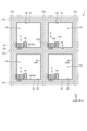
- FIG. 5 is a plan view showing the detection device according to the first embodiment.
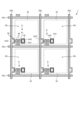
- FIG. 6 is a plan view schematically showing the detection device according to the first embodiment.
- 7 is a plan view schematically showing a first electrode and a transistor of the detection device according to the first embodiment; FIG. In FIG. 6, the insulating film 95 is hatched for easy viewing of the drawing.
- FIG. 7 is a plan view schematically showing a portion of the detection device excluding the insulating film of FIG.
- a control board 121 is electrically connected to the board 21 via a flexible printed board 71 .
- a detection circuit 48 is provided on the flexible printed circuit board 71 .
- a control circuit 122 and a power supply circuit 123 are provided on the control board 121 .
- the control circuit 122 is, for example, an FPGA (Field Programmable Gate Array).
- the control circuit 122 supplies control signals to the sensor section 10 , the gate line drive circuit 15 and the signal line selection circuit 16 to control the detection operation of the sensor section 10 .
- the power supply circuit 123 supplies voltage signals such as the sensor power supply signal VDDSNS (see FIG. 4) to the sensor section 10, the gate line drive circuit 15, and the signal line selection circuit 16.
- the substrate 21 has a detection area AA and a peripheral area GA.
- the detection area AA is an area including areas overlapping with the plurality of first electrodes 23 of the sensor section 10 .
- the peripheral area GA is an area outside the detection area AA and is an area that does not overlap with the first electrode 23 . That is, the peripheral area GA is an area between the outer circumference of the detection area AA and the edge of the substrate 21 .
- the gate line drive circuit 15 and the signal line selection circuit 16 are provided in the peripheral area GA.
- the plurality of first electrodes 23 are detection electrodes of the photodiodes PD, and output electrical signals according to the light irradiated thereon.
- a plurality of first electrodes 23 of the sensor section 10 are arranged in a matrix in the detection area AA.
- the plurality of first electrodes 23 outputs an electrical signal corresponding to the light irradiated thereon to the signal line selection circuit 16 as the detection signal Vdet.
- the detection device 1 detects information about the living body based on detection signals Vdet from the plurality of first electrodes 23 .
- the photodiode PD functions as a biosensor.
- the plurality of first electrodes 23 performs detection according to the gate drive signal Vgcl supplied from the gate line drive circuit 15 .
- the gate line drive circuit 15 and the signal line selection circuit 16 are provided in the peripheral area GA. Specifically, the gate line driving circuit 15 is provided in a region extending along the second direction Dy in the peripheral region GA.
- the signal line selection circuit 16 is provided in an area extending along the first direction Dx in the peripheral area GA, and is provided between the sensor section 10 and the detection circuit 48 .
- the second electrode 24 covers the detection area AA and has an area larger than the detection area AA.
- a conductive wiring 56 is arranged in the peripheral area GA, and the conductive wiring 56 and the second electrode 24 are electrically connected by a connection terminal 55 .
- the conductive wiring 56 is connected to the power supply circuit 123 shown in FIG. 1, and the sensor power supply signal VDDSNS is supplied to the conductive wiring 56 .
- the photodiode PD, the first electrode 23 and the first switching element Tr are provided in a region surrounded by the gate line GCL and the signal line SGL.
- the first electrode 23 is a lower electrode (cathode electrode) of the photodiode PD, and the plurality of photodiodes PD and the plurality of first electrodes 23 are arranged in a matrix above the substrate 21 .
- the insulating film 95 is provided between the adjacent first electrodes 23 and covers the outer periphery of the first electrodes 23 . More specifically, the insulating film 95 includes a first portion 95a extending in the first direction Dx and a second portion 95b extending in the second direction Dy. The insulating film 95 is provided in a grid pattern by intersecting the plurality of first portions 95a and the plurality of second portions 95b.
- the first portion 95a is provided so as to overlap with the gate line GCL, and is provided between the first electrodes 23 adjacent in the second direction Dy with the gate line GCL interposed therebetween.
- the second portion 95b is provided so as to overlap the signal line SGL, and is provided between the first electrodes 23 adjacent in the first direction Dx with the signal line SGL interposed therebetween.
- the multiple first electrodes 23 are partitioned by the insulating film 95 .
- the plurality of first electrodes 23 are connected to the lower buffer layer 32 (see FIG. 8) of the photodiode PD through openings OP formed in the insulating film 95 .
- the lower buffer layer 32 is an electron transport layer.
- the first switching element Tr has a semiconductor layer 61, a source electrode 62, a drain electrode 63 and a gate electrode 64.
- the semiconductor layer 61 extends along the gate line GCL and is provided to cross the gate electrode 64 in plan view.
- Gate electrode 64 is connected to gate line GCL and extends in a direction orthogonal to gate line GCL.
- One end side of the semiconductor layer 61 is connected to the source electrode 62 via the second contact hole CH2.
- the first electrode 23 is electrically connected to the source electrode 62 of the first switching element Tr through the first contact hole CH1. Thereby, the first switching element Tr is electrically connected to the photodiode PD.
- the other end side of the semiconductor layer 61 is connected to the drain electrode 63 through the third contact hole CH3. Drain electrode 63 is connected to signal line SGL.
- the second organic insulating film 96 is provided to cover the first contact hole CH1.
- Detailed configurations of the second organic insulating film 96 and the photodiode PD will be described with reference to FIG.
- the configuration and arrangement of the first switching element Tr shown in FIGS. 6 and 7 are merely examples, and can be changed as appropriate.
- FIG. 8 is a cross-sectional view taken along line VIII-VIII' of FIG.
- the detection device 1 includes a substrate 21, a first switching element Tr, a first organic insulating film 94, a first electrode 23, an insulating film 95, a second organic insulating film 96, It has an organic photodiode layer PDL, a second electrode 24 , sealing films 97 a , 97 b , 97 c and a resin mask 98 .
- the substrate 21 is an insulating base material, for example, glass or resin material is used.
- the substrate 21 is not limited to a flat plate shape, and may have a curved surface. In this case, the substrate 21 may be a film-like resin.
- the direction from the substrate 21 toward the organic photodiode layer PDL in the direction perpendicular to the surface of the substrate 21 is referred to as “upper” or simply “upper”. Also, the direction from the organic photodiode layer PDL to the substrate 21 is referred to as “lower side” or simply “lower side.”
- the light shielding film 65 is provided on the substrate 21 .
- a light shielding film 65 is provided between the semiconductor layer 61 and the substrate 21 .
- the light shielding film 65 can prevent light from entering the channel region of the semiconductor layer 61 from the substrate 21 side.
- the undercoat film 91 is provided on the substrate 21 covering the light shielding film 65 .
- the undercoat film 91 is made of, for example, an inorganic insulating film such as a silicon nitride film or a silicon oxide film.
- the structure of the undercoat film 91 is not limited to a single layer film, and may be a laminated film in which a plurality of inorganic insulating films are laminated.
- An undercoat film may also be provided between the substrate 21 and the light shielding film 65 .
- a plurality of first switching elements Tr are provided on the substrate 21 .
- the semiconductor layer 61 is provided on the undercoat film 91 .
- Polysilicon for example, is used for the semiconductor layer 61 .
- the semiconductor layer 61 is not limited to this, and may be a microcrystalline oxide semiconductor, an amorphous oxide semiconductor, a low-temperature polysilicon, or the like. Although only an n-type TFT is shown as the first switching element Tr, a p-type TFT may be formed at the same time.
- the gate insulating film 92 is provided on the undercoat film 91 to cover the semiconductor layer 61 .
- the gate insulating film 92 is, for example, an inorganic insulating film such as a silicon oxide film.
- Gate electrode 64 is provided on gate insulating film 92 .
- the first switching element Tr has a top gate structure.
- the first switching element Tr may have a bottom-gate structure or a dual-gate structure in which the gate electrodes 64 are provided on both the upper and lower sides of the semiconductor layer 61 .
- An interlayer insulating film 93 is provided on the gate insulating film 92 to cover the gate electrode 64 .
- the interlayer insulating film 93 has, for example, a laminated structure of a silicon nitride film and a silicon oxide film.
- a source electrode 62 and a drain electrode 63 are provided on the interlayer insulating film 93 .
- the source electrode 62 is connected to the source region of the semiconductor layer 61 through a second contact hole CH2 provided in the gate insulating film 92 and the interlayer insulating film 93.
- the drain electrode 63 is connected to the drain region of the semiconductor layer 61 through a third contact hole CH3 provided in the gate insulating film 92 and the interlayer insulating film 93. As shown in FIG.
- the first organic insulating film 94 is provided on the interlayer insulating film 93 to cover the source electrode 62 and the drain electrode 63 of the first switching element Tr.
- the first organic insulating film 94 is an organic planarizing film, and is superior in wiring step coverage and surface flatness compared to inorganic insulating materials formed by CVD or the like.
- the organic photodiode layer PDL is provided on the first organic insulating film 94 .
- the first electrode 23 and the insulating film 95 are provided between the substrate 21 and the first organic insulating film 94 and the organic photodiode layer PDL in a direction perpendicular to the surface of the substrate 21 .
- the first electrode 23 is provided on the first organic insulating film 94 and is provided to cover the bottom and inner side surfaces of the first contact hole CH1 formed in the first organic insulating film 94.
- the first electrode 23 is connected to the source electrode 62 of the first switching element Tr at the bottom surface of the first contact hole CH1.
- the first electrode 23 is a cathode electrode of the organic photodiode layer PDL, and is formed of, for example, a translucent conductive material such as ITO (Indium Tin Oxide) or IZO (Indium Zinc Oxide).
- the plurality of first electrodes 23 are arranged separately for each detection element PAA (photodiode PD).
- the organic photodiode layer PDL has an area larger than that of the first electrode 23 in plan view, and covers the upper surface of the first electrode 23 and the outer edge portion 23e.
- the insulating film 95 is provided between the adjacent first electrodes 23 and covers the outer edge portion 23 e of the first electrode 23 .
- the insulating film 95 is an inorganic insulating film, and a material such as a silicon nitride film or an aluminum oxide film is used.
- the insulating film 95 has at least one or more openings OP (see FIG. 6) in a region overlapping with the top surface of the first electrode 23 .
- the organic photodiode layer PDL is electrically connected to the first electrode 23 through the opening OP.
- the insulating film 95 is provided between the first organic insulating film 94 and the organic photodiode layer PDL in the region between the adjacent first electrodes 23 . Thereby, the insulating film 95 insulates the adjacent first electrodes 23 . In other words, the insulating film 95 can suppress leakage current between adjacent photodiodes PD.
- the insulating film 95 also functions as a barrier film that suppresses the entry of moisture from the first organic insulating film 94 into the organic photodiode layer PDL in the region between the adjacent first electrodes 23 .
- the second organic insulating film 96 is provided to cover the inside of the first contact hole CH1.
- the first electrode 23 and the second organic insulating film 96 are stacked on the inner and bottom surfaces of the first contact hole CH1.
- a first organic insulating film 94, a first electrode 23, and a second organic insulating film 96 are stacked in this order on the inner surface of the first contact hole CH1.
- On the bottom surface of the first contact hole CH1, the first electrode 23 and the second organic insulating film 96 are stacked in this order on the source electrode 62.
- the second organic insulating film 96 is provided to cover the corner portion 23t of the first electrode 23 at a position overlapping the opening end portion of the first contact hole CH1.
- the organic photodiode layer PDL is provided covering the plurality of first electrodes 23, the insulating film 95 and the second organic insulating film 96. More specifically, the organic photodiode layer PDL includes an active layer 31, a lower buffer layer 32 (first carrier transport layer), and an upper buffer layer 33 (second carrier transport layer). A lower buffer layer 32 (first carrier transport layer) is provided between the active layer 31 and the first electrode 23 . An upper buffer layer 33 (second carrier transport layer) is provided between the active layer 31 and the second electrode 24 . The upper buffer layer 33 is a hole transport layer.
- the lower buffer layer 32 is formed by applying a material such as zinc acetate, ethoxylated polyethyleneimine (PEIE), polyethyleneimine (PEI), or the like.
- the lower buffer layer 32 is a single layer and has a thickness of, for example, about 30 nm or less.
- a mixture of a p-type organic semiconductor and an n-type organic semiconductor is used for the active layer 31 .
- a p-type organic semiconductor for example, PMDPP3T (poly((2,5-bis(2-hexyldecyl)-2,3,5,6-tetrahydro-3,6-dioxopyrrolo(3,4-c)pyrrole-1,4 -diyl)-alt-(3′,3′′-dimethyl-2,2′:5′,2′′-terthiophene)-5,5′′-diyl)).
- examples of n-type organic semiconductors include PC61BM ([6,6]-phenyl C61-butyric acid methyl ester).
- the thickness of the active layer 31 is, for example, about 100 nm or more and 500 nm or less, preferably about 350 nm.
- the upper buffer layer 33 is, for example, a metal oxide layer such as tungsten oxide (WO 3 ) or molybdenum oxide (MoOx).
- the upper buffer layer 33 is formed of a deposited film or a sputtered film, and its thickness is, for example, about 30 nm or less.
- the lower buffer layer 32 , the active layer 31 and the upper buffer layer 33 forming the organic photodiode layer PDL are provided covering the plurality of first electrodes 23 , the insulating film 95 and the second organic insulating film 96 .
- the lower buffer layer 32 is connected to the first electrode 23 in a region overlapping the opening OP of the insulating film 95 .
- the lower buffer layer 32 includes an overlapping portion 32s provided on the insulating film 95 and an overlapping portion 32t provided on the second organic insulating film 96 in a region overlapping with the first contact hole CH1. include.
- the detection device 1 includes a first organic insulating film 94 , a first electrode 23 , a lower buffer layer 32 , an active layer 31 , an upper buffer layer 33 , a second
- the electrodes 24 are stacked in order.
- the first electrode 23, the second organic insulating film 96, the lower buffer layer 32 (overlapping portion 32t), the active layer 31, the upper buffer layer 33, and the second electrode 24 are laminated in this order. be done.
- the first organic insulating film 94, the insulating film 95, the lower buffer layer 32 (overlapping portion 32s), the active layer 31, the upper buffer layer 33, and the second electrode 24 are arranged in this order. Laminated.
- the insulating film 95 is provided between the adjacent first electrodes 23 and covers the outer edges 23e of the first electrodes 23 .
- the thickness of the lower buffer layer 32 is formed thin at the position overlapping with the outer edge portion 23 e of the first electrode 23 .
- the insulating film 95 provides a gap between the active layer 31 and the first electrode 23 . It is possible to suppress the occurrence of short circuits.
- FIG. 8 shows a case where the superimposed portion 32s and the lower buffer layer 32 on the first electrode 23 are formed apart from each other in order to facilitate understanding, but the superimposed portion 32s,
- the lower buffer layer 32 on the first electrode 23 may be formed continuously and integrally.
- the second organic insulating film 96 is provided to cover the inside of the first contact hole CH1, covering the corner 23t of the first electrode 23 formed at the opening end of the first contact hole CH1.
- the region overlapping the first contact hole CH1 is planarized, and the overlapping portion 32t of the lower buffer layer 32 is formed continuously with the lower buffer layer 32 above the first electrode 23.
- the second organic insulating film 96 covers most of the region of the first electrode 23 inside the first contact hole CH1. Therefore, even if part of the lower buffer layer 32 is thinly formed or the lower buffer layer 32 is cut off in the region overlapping with the first contact hole CH1, the second organic insulating film 96 prevents the active layer from being formed. The occurrence of a short circuit between 31 and first electrode 23 can be suppressed.
- the organic insulating film 96 extends over the region overlapping with the first contact hole CH1 and the region not overlapping with the first contact hole CH1. Variations in film thickness of the active layer 31, the lower buffer layer 32, and the upper buffer layer 33 that form the photodiode layer PDL are suppressed. That is, compared to the configuration in which the second organic insulating film 96 is not provided, the active layer 31, the lower buffer layer 32, and the upper buffer layer 33 are not cut or thinned in the region overlapping the first contact hole CH1. Suppressed. Thereby, the detection device 1 can suppress leakage current between the anode and the cathode of the photodiode PD.
- the second electrode 24 is an upper electrode provided on the organic photodiode layer PDL. More specifically, the second electrode 24 is provided on the upper buffer layer 33 of the organic photodiode layer PDL.
- the second electrode 24 is an anode electrode of the photodiode PD, and is formed continuously over the plurality of detection elements PAA (photodiodes PD).
- the second electrode 24 is made of a metal material such as silver (Ag), and functions as a reflective electrode.
- the second electrode 24 is not limited to this, and the second electrode 24 may be made of a conductive material having translucency like the first electrode 23 .
- the sealing films 97 a , 97 b , 97 c are provided on the second electrode 24 .
- an inorganic insulating film such as a silicon nitride film or an aluminum oxide film is used.
- a resin film such as acrylic is used.
- the sealing films 97a, 97b, and 97c are not limited to laminated films in which an inorganic insulating film and an organic insulating film are laminated, and may be a single layer.
- a resin mask 98 is provided covering the sealing film 97c.
- the organic photodiode layer PDL is well sealed by the sealing films 97a, 97b, and 97c and the resin mask 98, and it is possible to suppress penetration of moisture from the upper surface side.
- the thickness of the first electrode 23 is, for example, about 50 nm.
- the thickness of the second electrode 24 is, for example, about 100 nm or less. That is, the lower buffer layer 32 and the upper buffer layer 33 are each thinner than the active layer 31 and thinner than the first electrode 23 and the second electrode 24 . In other words, the thickness of each of the first electrode 23 and the second electrode 24 is thinner than the active layer 31 and thicker than the lower buffer layer 32 and the upper buffer layer 33 .
- the materials and manufacturing methods of the lower buffer layer 32, the active layer 31, and the upper buffer layer 33 are merely examples, and other materials and manufacturing methods may be used.
- the lower buffer layer 32 may be a deposited film or sputtered film using materials such as zinc oxide (ZnO) and titanium oxide (TiO 2 ).
- the upper buffer layer 33 may be a deposited film or sputtered film using a material such as nickel oxide (NiO), or the upper buffer layer 33 may be vanadium oxide (V 2 O 5 ) or tungsten oxide ( WO 3 ) or the like, or a material such as PEDOT:PSS, may be used for coating.
- planar shape and cross-sectional shape of the insulating film 95 and the second organic insulating film 96 shown in FIGS. 6 and 8 are only schematic, and can be changed as appropriate.
- the upper surface of the second organic insulating film 96 is not limited to a configuration having a curved surface, and a portion of the upper surface may be formed flat.
- the planar shape of the second organic insulating film 96 is not limited to a square shape, and may be other shapes such as a circular shape, a polygonal shape, etc. according to the planar shape of the first contact hole CH1.
- the opening OP formed in the insulating film 95 is not limited to a rectangular shape, and can be changed as appropriate according to the shape of the first electrode 23 .
- FIG. 9 is a cross-sectional view taken along line IX-IX' of FIG.
- the second electrodes 24 connect to conductive traces 56 in a peripheral area GA around the sensing area AA.
- the organic photodiode layer PDL has a non-formation region in the peripheral region GA, and the side surface 33e of the upper buffer layer 33, the side surface 31e of the active layer 31, and the side surface 32e of the lower buffer layer 32 are exposed at the ends.
- the side surface 33e of the upper buffer layer 33, the side surface 31e of the active layer 31, and the side surface 32e of the lower buffer layer 32 are the side surface PDLe of the organic photodiode layer PDL.
- the second electrode 24 provided covering the side surface PDLe of the organic photodiode layer PDL is electrically connected to the side surface 33 e of the upper buffer layer 33 , the side surface 31 e of the active layer 31 and the side surface 32 e of the lower buffer layer 32 . Therefore, the second electrode 24 is laminated on the exposed side surface PDLe of the organic photodiode layer PDL in the peripheral region GA, and a leakage current may flow between the second electrode 24 and the outermost first electrode 23.
- a third electrode is provided between the second electrode 24 on the side surface PDLe of the organic photodiode layer PDL and the outermost first electrode 23. 25 are formed.
- connection terminals 55 are formed in the peripheral area GA. Conductive wiring 56 is formed on undercoat film 91 .
- the connection terminal 55 has a conductive pedestal portion 57 electrically connected to the conductive wiring 56, and a terminal electrode 23a electrically connected to the pedestal portion 57 via the contact hole CHA.
- a second organic insulating film 96 is provided to cover the inside of the contact hole CHA.
- the terminal electrode 23 a is electrically connected to the second electrode 24 .
- the third electrode 25 is electrically connected to the reference potential wiring 26 via the contact hole CHC.
- the reference potential wiring 26 is routed along the outermost circumference of the first electrode 23 .
- the third electrode 25 has the same potential as the reference signal, which is the reset potential supplied from the reset circuit 17 to the signal line SGL. As a result, the potential difference between the third electrode 25 and the first electrode 23 is reduced, and a leak current from the third electrode 25 to the first electrode 23 is less likely to occur.
- leakage current from the second electrode 24 to the third electrode 25 becomes a problem during a period in which light detection is not performed, the same potential as that of the second electrode 24 is supplied to the reference potential wiring 26 . can be As a result, the potential difference between the third electrode 25 and the second electrode 24 is reduced, and a leak current from the second electrode 24 to the third electrode 25 is less likely to occur.
- the second organic insulating film 96 is provided to cover the inside of the contact hole CHC.
- the third electrode 25 is routed along the outermost periphery of the first electrode 23 and surrounds the first electrode 23 in a square shape. Thus, the third electrode 25 surrounds the entire outermost periphery of the first electrode 23 .
- the second electrode 24 is electrically connected to a conductive wiring 56 drawn around the peripheral area GA outside the third electrode 25 .
- the detection device 1 of the first embodiment includes a plurality of photodiodes PD provided on the substrate 21, a plurality of first electrodes 23, a second electrode 24, a third electrode 25, and an organic photodiode PD.
- a diode layer PDL is provided.
- the plurality of first electrodes 23 are provided corresponding to each of the plurality of photodiodes PD.
- the second electrode 24 is provided across the plurality of photodiodes PD.
- the organic photodiode layer PDL includes a lower buffer layer 32 (first carrier transport layer), an active layer 31 and an upper buffer layer 33 (second carrier transport layer), and is provided across a plurality of photodiodes PD.
- the plurality of photodiodes PD includes the first electrode 23, the lower buffer layer 32 (first carrier transport layer), the active layer 31 and the upper buffer layer 33 (second carrier transport layer). layer), and the second electrode 24 are stacked in this order.
- a reference potential is supplied to the third electrode 25 .
- the third electrode 25 is arranged between the second electrode 24 provided to cover the side surface PDLe of the organic photodiode layer PDL outside the detection area AA and the first electrode 23 arranged on the outermost periphery. .
- FIG. 10 is a plan view showing the detection device according to the second embodiment.
- the same reference numerals are assigned to the same components as those described in the above-described embodiment, and overlapping descriptions will be omitted.
- the conductive wiring 56 is arranged in a U-shape in the peripheral area GA, and the conductive wiring 56 and the second It is electrically connected to the electrode 24 .
- the conductive wiring 56 is connected to the power supply circuit 123 shown in FIG. 1, and the sensor power supply signal VDDSNS is supplied to the conductive wiring 56 .
- the third electrode 25 is routed along the outermost periphery of the first electrode 23 and surrounds the first electrode 23 in a U-shape.
- the third electrode 25 is arranged except for one side of the sides surrounding the outermost periphery of the first electrode 23 .
- the second electrode 24 is arranged inside the side surface PDLe of the organic photodiode layer PDL. That is, in the region where the third electrode 25 is not arranged, the second electrode 24 is not laminated on the side surface PDLe of the organic photodiode layer PDL. This suppresses leakage current in the region where the third electrode 25 is not arranged.
- FIG. 11 is a plan view showing the detection device according to the third embodiment.
- the same reference numerals are assigned to the same components as those described in the above-described embodiment, and overlapping descriptions will be omitted.
- the conductive wiring 56 is linearly arranged in a part of the peripheral area GA, and the conductive wiring 56 is connected to the connection terminal 55. It is electrically connected to the second electrode 24 .
- the conductive wiring 56 is connected to the power supply circuit 123 shown in FIG. 1, and the sensor power supply signal VDDSNS is supplied to the conductive wiring 56 .
- the third electrode 25 is routed along the outermost periphery of the first electrode 23 and arranged in a straight line.
- the third electrode 25 is arranged only on one side of the sides surrounding the outermost periphery of the first electrode 23 .
- the second electrode 24 is arranged inside the side surface PDLe of the organic photodiode layer PDL. That is, in the region where the third electrode 25 is not arranged, the second electrode 24 is not laminated on the side surface PDLe of the organic photodiode layer PDL. This suppresses leakage current in the regions of the plurality of sides where the third electrode 25 is not arranged.
Abstract
The present invention provides a detection device which is capable of suppressing the occurrence of a short circuit between a second electrode and a first electrode that is on the outermost periphery. This detection device comprises a substrate and a plurality of photodiodes which are provided in a detection region of the substrate. The photodiodes each comprise a first electrode, a second electrode, a first carrier transport layer, an active layer and a second carrier transport layer, while comprising an organic photodiode layer that is provided so as to extend across a plurality of photodiodes. In the detection region, the first electrode, the first carrier transport layer, the active layer, the second carrier transport layer and the second electrode are sequentially stacked. On the outside of the detection region, a third electrode, to which the reference potential is applied, is arranged between the second electrode, which is provided so as to cover the lateral surface of the organic photodiode layer, and the first electrode, which is arranged on the outermost periphery.
Description
本開示は、検出装置に関する。
The present disclosure relates to a detection device.
指紋パターンや静脈パターンを検出可能な光センサが知られている(例えば、特許文献1)。このような光センサは、活性層として有機半導体材料が用いられた複数のフォトダイオードを有する。特許文献2に記載されるように、フォトダイオードは、下部電極と上部電極との間に配置され、例えば、下部電極、電子輸送層、活性層、正孔輸送層、上部電極の順に積層される。電子輸送層又は正孔輸送層は、バッファ層とも呼ばれる。
An optical sensor capable of detecting fingerprint patterns and vein patterns is known (for example, Patent Document 1). Such photosensors have a plurality of photodiodes in which organic semiconductor materials are used as active layers. As described in Patent Document 2, the photodiode is arranged between the lower electrode and the upper electrode, and for example, the lower electrode, the electron transport layer, the active layer, the hole transport layer, and the upper electrode are stacked in this order. . An electron-transporting layer or a hole-transporting layer is also called a buffer layer.
上部電極は、検出領域の周りの額縁領域で配線に接続する。上部電極は、額縁領域において、活性層及びバッファ層の側面に積層され、上部電極と最外周の下部電極との間にリーク電流が流れる可能性がある。
The upper electrode connects to wiring in the frame area around the detection area. The upper electrode is stacked on the side surfaces of the active layer and the buffer layer in the frame region, and a leak current may flow between the upper electrode and the outermost lower electrode.
本開示は、第2電極と最外周の第1電極との間の短絡の発生を抑制することが可能な検出装置を提供することを目的とする。
An object of the present disclosure is to provide a detection device capable of suppressing the occurrence of a short circuit between the second electrode and the outermost first electrode.
本開示の一態様の検出装置は、基板と、前記基板の検出領域に設けられた複数のフォトダイオードと、を含み、前記フォトダイオードは、複数の前記フォトダイオードのそれぞれに対応して設けられた複数の第1電極と、複数の前記フォトダイオードに跨がって設けられる第2電極と、第1キャリア輸送層、活性層及び第2キャリア輸送層を含み、複数の前記フォトダイオードに跨がって設けられる有機フォトダイオード層と、を含み、前記検出領域では、前記第1電極、前記第1キャリア輸送層、前記活性層、前記第2キャリア輸送層、及び前記第2電極が順に積層され、前記検出領域の外側において、前記有機フォトダイオード層の側面を覆って設けられる前記第2電極と、最外周に配置された前記第1電極との間に、基準電位が供給される第3電極が配置されている。
A detection device according to one aspect of the present disclosure includes a substrate and a plurality of photodiodes provided in a detection region of the substrate, wherein the photodiodes are provided corresponding to each of the plurality of photodiodes. a plurality of first electrodes; a second electrode provided across the plurality of photodiodes; a first carrier transport layer; an active layer; and a second carrier transport layer; and an organic photodiode layer provided in the detection region, wherein the first electrode, the first carrier transport layer, the active layer, the second carrier transport layer, and the second electrode are stacked in order, Outside the detection region, a third electrode to which a reference potential is supplied is provided between the second electrode provided covering the side surface of the organic photodiode layer and the first electrode disposed on the outermost periphery. are placed.
本開示を実施するための形態(実施形態)につき、図面を参照しつつ詳細に説明する。以下の実施形態に記載した内容により本開示が限定されるものではない。また、以下に記載した構成要素には、当業者が容易に想定できるもの、実質的に同一のものが含まれる。さらに、以下に記載した構成要素は適宜組み合わせることが可能である。なお、開示はあくまで一例にすぎず、当業者において、本開示の主旨を保っての適宜変更について容易に想到し得るものについては、当然に本開示の範囲に含有されるものである。また、図面は説明をより明確にするため、実際の態様に比べ、各部の幅、厚さ、形状等について模式的に表される場合があるが、あくまで一例であって、本開示の解釈を限定するものではない。また、本開示と各図において、既出の図に関して前述したものと同様の要素には、同一の符号を付して、詳細な説明を適宜省略することがある。
A form (embodiment) for carrying out the present disclosure will be described in detail with reference to the drawings. The present disclosure is not limited by the contents described in the following embodiments. In addition, the components described below include those that can be easily assumed by those skilled in the art and those that are substantially the same. Furthermore, the components described below can be combined as appropriate. It should be noted that the disclosure is merely an example, and those skilled in the art can easily conceive appropriate modifications while maintaining the gist of the present disclosure are naturally included in the scope of the present disclosure. In addition, in order to make the description clearer, the drawings may schematically show the width, thickness, shape, etc. of each part compared to the actual embodiment, but this is only an example, and the interpretation of the present disclosure is not intended. It is not limited. In addition, in the present disclosure and each figure, elements similar to those described above with respect to previous figures may be denoted by the same reference numerals, and detailed description thereof may be omitted as appropriate.
本実施形態及び請求の範囲において、ある構造体の上に他の構造体を配置する態様を表現するにあたり、単に「上に」と表記する場合、特に断りの無い限りは、ある構造体に接するように、直上に他の構造体を配置する場合と、ある構造体の上方に、さらに別の構造体を介して他の構造体を配置する場合との両方を含むものとする。
In the present embodiment and the scope of the claims, when expressing a mode in which another structure is arranged on top of a structure, when simply writing “above”, unless otherwise specified, it is in contact with the structure. Thus, it includes both the case of arranging another structure directly above and the case of arranging another structure above a certain structure via another structure.
(第1実施形態)
図1は、第1実施形態に係る検出装置を示す模式図である。図1に示すように、検出装置1は、基板21と、センサ部10と、ゲート線駆動回路15と、信号線選択回路16と、検出回路48と、制御回路122と、電源回路123と、第1光源基材51と、第2光源基材52と、第1光源53と、第2光源54と、を有する。第1光源基材51には、複数の第1光源53が設けられる。第2光源基材52には複数の第2光源54が設けられる。 (First embodiment)
FIG. 1 is a schematic diagram showing a detection device according to the first embodiment. As shown in FIG. 1, thedetection device 1 includes a substrate 21, a sensor section 10, a gate line drive circuit 15, a signal line selection circuit 16, a detection circuit 48, a control circuit 122, a power supply circuit 123, It has a first light source substrate 51 , a second light source substrate 52 , a first light source 53 , and a second light source 54 . A plurality of first light sources 53 are provided on the first light source substrate 51 . A plurality of second light sources 54 are provided on the second light source substrate 52 .
図1は、第1実施形態に係る検出装置を示す模式図である。図1に示すように、検出装置1は、基板21と、センサ部10と、ゲート線駆動回路15と、信号線選択回路16と、検出回路48と、制御回路122と、電源回路123と、第1光源基材51と、第2光源基材52と、第1光源53と、第2光源54と、を有する。第1光源基材51には、複数の第1光源53が設けられる。第2光源基材52には複数の第2光源54が設けられる。 (First embodiment)
FIG. 1 is a schematic diagram showing a detection device according to the first embodiment. As shown in FIG. 1, the
基板21には、フレキシブルプリント基板71を介して制御基板121が電気的に接続される。フレキシブルプリント基板71は、例えば、フレキシブルプリント基板やリジット基板である。フレキシブルプリント基板71には、検出回路48が設けられている。制御基板121には、制御回路122及び電源回路123が設けられている。制御回路122は、例えばFPGA(Field Programmable Gate Array)である。制御回路122は、センサ部10、ゲート線駆動回路15及び信号線選択回路16に制御信号を供給して、センサ部10の検出動作を制御する。また、制御回路122は、第1光源53及び第2光源54に制御信号を供給して、第1光源53及び第2光源54の点灯又は非点灯を制御する。電源回路123は、センサ電源信号VDDSNS(図4参照)等の電圧信号をセンサ部10、ゲート線駆動回路15及び信号線選択回路16に供給する。また、電源回路123は、電源電圧を第1光源53及び第2光源54に供給する。
A control board 121 is electrically connected to the board 21 via a flexible printed board 71 . The flexible printed board 71 is, for example, a flexible printed board or a rigid board. A detection circuit 48 is provided on the flexible printed circuit board 71 . A control circuit 122 and a power supply circuit 123 are provided on the control board 121 . The control circuit 122 is, for example, an FPGA (Field Programmable Gate Array). The control circuit 122 supplies control signals to the sensor section 10 , the gate line drive circuit 15 and the signal line selection circuit 16 to control the detection operation of the sensor section 10 . The control circuit 122 also supplies control signals to the first light source 53 and the second light source 54 to control lighting or non-lighting of the first light source 53 and the second light source 54 . The power supply circuit 123 supplies voltage signals such as the sensor power supply signal VDDSNS (see FIG. 4) to the sensor section 10, the gate line drive circuit 15, and the signal line selection circuit 16. FIG. Also, the power supply circuit 123 supplies a power supply voltage to the first light source 53 and the second light source 54 .
基板21は、検出領域AAと、周辺領域GAとを有する。検出領域AAは、センサ部10が有する複数のフォトダイオードPD(図4参照)が設けられた領域である。周辺領域GAは、検出領域AAの外周と、基板21の外縁部との間の領域であり、複数のフォトダイオードPDが設けられない領域である。
The substrate 21 has a detection area AA and a peripheral area GA. The detection area AA is an area in which a plurality of photodiodes PD (see FIG. 4) of the sensor section 10 are provided. The peripheral area GA is an area between the outer circumference of the detection area AA and the outer edge of the substrate 21, and is an area in which the plurality of photodiodes PD are not provided.
ゲート線駆動回路15及び信号線選択回路16は、周辺領域GAに設けられる。具体的には、ゲート線駆動回路15は、周辺領域GAのうち第2方向Dyに沿って延在する領域に設けられる。信号線選択回路16は、周辺領域GAのうち第1方向Dxに沿って延在する領域に設けられ、センサ部10と検出回路48との間に設けられる。
The gate line drive circuit 15 and the signal line selection circuit 16 are provided in the peripheral area GA. Specifically, the gate line driving circuit 15 is provided in a region extending along the second direction Dy in the peripheral region GA. The signal line selection circuit 16 is provided in an area extending along the first direction Dx in the peripheral area GA, and is provided between the sensor section 10 and the detection circuit 48 .
なお、以下の説明において、第1方向Dxは、基板21と平行な面内の一方向である。第2方向Dyは、基板21と平行な面内の一方向であり、第1方向Dxと直交する方向である。なお、第2方向Dyは、第1方向Dxと直交しないで交差してもよい。また、「平面視」とは、基板21と垂直な方向から見た場合の位置関係をいう。
It should be noted that in the following description, the first direction Dx is one direction within a plane parallel to the substrate 21 . The second direction Dy is one direction in a plane parallel to the substrate 21 and perpendicular to the first direction Dx. Note that the second direction Dy may cross the first direction Dx instead of being perpendicular to it. In addition, “planar view” refers to the positional relationship when viewed from a direction perpendicular to the substrate 21 .
複数の第1光源53は、第1光源基材51に設けられ、第2方向Dyに沿って配列される。複数の第2光源54は、第2光源基材52に設けられ、第2方向Dyに沿って配列される。第1光源基材51及び第2光源基材52は、それぞれ、制御基板121に設けられた端子部124、125を介して、制御回路122及び電源回路123と電気的に接続される。
The plurality of first light sources 53 are provided on the first light source substrate 51 and arranged along the second direction Dy. A plurality of second light sources 54 are provided on the second light source substrate 52 and arranged along the second direction Dy. The first light source base material 51 and the second light source base material 52 are electrically connected to a control circuit 122 and a power supply circuit 123 via terminal portions 124 and 125 provided on the control board 121, respectively.
複数の第1光源53及び複数の第2光源54は、例えば、無機LED(Light Emitting Diode)や、有機EL(OLED:Organic Light Emitting Diode)等が用いられる。複数の第1光源53及び複数の第2光源54は、それぞれ異なる波長の第1光及び第2光を出射する。
For the plurality of first light sources 53 and the plurality of second light sources 54, for example, inorganic LEDs (Light Emitting Diodes) or organic ELs (OLEDs: Organic Light Emitting Diodes) are used. The plurality of first light sources 53 and the plurality of second light sources 54 emit first light and second light with different wavelengths, respectively.
第1光源53から出射された第1光は、主に指等の被検出体の表面で反射されセンサ部10に入射する。これにより、センサ部10は、指等の表面の凹凸の形状を検出することで指紋を検出することができる。第2光源54から出射された第2光は、主に指等の内部で反射し又は指等を透過してセンサ部10に入射する。これにより、センサ部10は、指等の内部の生体に関する情報を検出できる。生体に関する情報とは、例えば、指や掌の脈波、脈拍、血管像等である。すなわち、検出装置1は、指紋を検出する指紋検出装置や、静脈などの血管パターンを検出する静脈検出装置として構成されてもよい。
The first light emitted from the first light source 53 is mainly reflected by the surface of the object to be detected such as a finger and enters the sensor section 10 . As a result, the sensor unit 10 can detect a fingerprint by detecting the uneven shape of the surface of the finger or the like. The second light emitted from the second light source 54 is mainly reflected inside the finger or the like or transmitted through the finger or the like and enters the sensor section 10 . Thereby, the sensor unit 10 can detect information about the internal living body such as a finger. The biological information includes, for example, finger and palm pulse waves, pulse, blood vessel images, and the like. That is, the detection device 1 may be configured as a fingerprint detection device that detects fingerprints or a vein detection device that detects blood vessel patterns such as veins.
第1光は、500nm以上600nm以下、例えば550nm程度の波長を有し、第2光は、780nm以上950nm以下、例えば850nm程度の波長を有していてもよい。この場合、第1光は、青色又は緑色の可視光であり、第2光は、赤外光である。センサ部10は、第1光源53から出射された第1光に基づいて、指紋を検出することができる。第2光源54から出射された第2光は、指等の被検出体の内部で反射し又は指等を透過・吸収されてセンサ部10に入射する。これにより、センサ部10は、指等の内部の生体に関する情報として脈波や血管像(血管パターン)を検出できる。
The first light may have a wavelength of 500 nm or more and 600 nm or less, for example about 550 nm, and the second light may have a wavelength of 780 nm or more and 950 nm or less, for example about 850 nm. In this case, the first light is blue or green visible light, and the second light is infrared light. The sensor unit 10 can detect a fingerprint based on the first light emitted from the first light source 53 . The second light emitted from the second light source 54 is reflected inside an object to be detected such as a finger or is transmitted/absorbed by the finger or the like and enters the sensor section 10 . As a result, the sensor unit 10 can detect a pulse wave and a blood vessel image (blood vessel pattern) as information about the internal living body of a finger or the like.
又は、第1光は、600nm以上700nm以下、例えば660nm程度の波長を有し、第2光は、780nm以上900nm以下、例えば850nm程度の波長を有していてもよい。この場合、第1光源53から出射された第1光及び第2光源54から出射された第2光に基づいて、センサ部10は、生体に関する情報として、脈波、脈拍や血管像に加えて、血中酸素飽和度を検出することができる。このように、検出装置1は、第1光源53及び複数の第2光源54を有しているので、第1光に基づいた検出と、第2光に基づいた検出とを行うことで、種々の生体に関する情報を検出することができる。
Alternatively, the first light may have a wavelength of 600 nm or more and 700 nm or less, for example about 660 nm, and the second light may have a wavelength of 780 nm or more and 900 nm or less, for example about 850 nm. In this case, based on the first light emitted from the first light source 53 and the second light emitted from the second light source 54, the sensor unit 10 obtains information about the living body in addition to the pulse wave, the pulse, and the blood vessel image. , can detect blood oxygen saturation. As described above, since the detection device 1 has the first light source 53 and the plurality of second light sources 54, by performing detection based on the first light and detection based on the second light, various can detect information about the living body of
なお、図1に示す第1光源53及び第2光源54の配置は、あくまで一例であり適宜変更することができる。検出装置1は、光源として複数種類の光源(第1光源53と第2光源54)が設けられている。ただし、これに限定されず、光源は1種類であってもよい。例えば、第1光源基材51及び第2光源基材52のそれぞれに、複数の第1光源53及び複数の第2光源54が配置されていてもよい。また、第1光源53及び第2光源54が設けられる光源基材は1つ又は3つ以上であってもよい。あるいは、光源は、少なくとも1つ以上配置されていればよい。
Note that the arrangement of the first light source 53 and the second light source 54 shown in FIG. 1 is merely an example and can be changed as appropriate. The detection device 1 is provided with a plurality of types of light sources (first light source 53 and second light source 54) as light sources. However, it is not limited to this, and the number of light sources may be one. For example, a plurality of first light sources 53 and a plurality of second light sources 54 may be arranged on each of the first light source substrate 51 and the second light source substrate 52 . Also, the number of light source substrates provided with the first light source 53 and the second light source 54 may be one or three or more. Alternatively, at least one light source may be arranged.
図2は、第1実施形態に係る検出装置の構成例を示すブロック図である。図2に示すように、検出装置1は、さらに検出制御部11と検出部40と、有する。検出制御部11の機能の一部又は全部は、制御回路122に含まれる。また、検出部40のうち、検出回路48以外の機能の一部又は全部は、制御回路122に含まれる。
FIG. 2 is a block diagram showing a configuration example of the detection device according to the first embodiment. As shown in FIG. 2 , the detection device 1 further has a detection control section 11 and a detection section 40 . A part or all of the functions of the detection control section 11 are included in the control circuit 122 . Also, part or all of the functions of the detection unit 40 other than the detection circuit 48 are included in the control circuit 122 .
センサ部10は、複数のフォトダイオードPDを有する。センサ部10が有するフォトダイオードPDは、照射される光に応じた電気信号を、検出信号Vdetとして信号線選択回路16に出力する。また、センサ部10は、ゲート線駆動回路15から供給されるゲート駆動信号Vgclにしたがって検出を行う。
The sensor unit 10 has a plurality of photodiodes PD. The photodiode PD included in the sensor unit 10 outputs an electrical signal corresponding to the irradiated light to the signal line selection circuit 16 as the detection signal Vdet. Further, the sensor section 10 performs detection according to the gate drive signal Vgcl supplied from the gate line drive circuit 15 .
検出制御部11は、ゲート線駆動回路15、信号線選択回路16及び検出部40にそれぞれ制御信号を供給し、これらの動作を制御する回路である。検出制御部11は、スタート信号STV、クロック信号CK、リセット信号RST1等の各種制御信号をゲート線駆動回路15に供給する。また、検出制御部11は、選択信号ASW等の各種制御信号を信号線選択回路16に供給する。また、検出制御部11は、各種制御信号を第1光源53及び第2光源54に供給して、それぞれの点灯及び非点灯を制御する。
The detection control unit 11 is a circuit that supplies control signals to the gate line drive circuit 15, the signal line selection circuit 16, and the detection unit 40, respectively, and controls their operations. The detection control unit 11 supplies various control signals such as a start signal STV, a clock signal CK, and a reset signal RST1 to the gate line drive circuit 15 . The detection control unit 11 also supplies various control signals such as the selection signal ASW to the signal line selection circuit 16 . The detection control unit 11 also supplies various control signals to the first light source 53 and the second light source 54 to control lighting and non-lighting of each.
ゲート線駆動回路15は、各種制御信号に基づいて複数のゲート線GCL(図3参照)を駆動する回路である。ゲート線駆動回路15は、複数のゲート線GCLを順次又は同時に選択し、選択されたゲート線GCLにゲート駆動信号Vgclを供給する。これにより、ゲート線駆動回路15は、ゲート線GCLに接続された複数のフォトダイオードPDを選択する。
The gate line drive circuit 15 is a circuit that drives a plurality of gate lines GCL (see FIG. 3) based on various control signals. The gate line driving circuit 15 sequentially or simultaneously selects a plurality of gate lines GCL and supplies a gate driving signal Vgcl to the selected gate lines GCL. Thereby, the gate line drive circuit 15 selects a plurality of photodiodes PD connected to the gate line GCL.
信号線選択回路16は、複数の信号線SGL(図3参照)を順次又は同時に選択するスイッチ回路である。信号線選択回路16は、例えばマルチプレクサである。信号線選択回路16は、検出制御部11から供給される選択信号ASWに基づいて、選択された信号線SGLと検出回路48とを接続する。これにより、信号線選択回路16は、フォトダイオードPDの検出信号Vdetを検出部40に出力する。
The signal line selection circuit 16 is a switch circuit that sequentially or simultaneously selects a plurality of signal lines SGL (see FIG. 3). The signal line selection circuit 16 is, for example, a multiplexer. The signal line selection circuit 16 connects the selected signal line SGL and the detection circuit 48 based on the selection signal ASW supplied from the detection control section 11 . Thereby, the signal line selection circuit 16 outputs the detection signal Vdet of the photodiode PD to the detection section 40 .
検出部40は、検出回路48と、信号処理回路44と、座標抽出回路45と、記憶回路46と、検出タイミング制御回路47と、画像処理回路49と、出力処理部50とを備える。検出タイミング制御回路47は、検出制御部11から供給される制御信号に基づいて、検出回路48と、信号処理回路44と、座標抽出回路45と、画像処理回路49と、が同期して動作するように制御する。
The detection unit 40 includes a detection circuit 48 , a signal processing circuit 44 , a coordinate extraction circuit 45 , a storage circuit 46 , a detection timing control circuit 47 , an image processing circuit 49 and an output processing unit 50 . The detection timing control circuit 47 operates in synchronization with the detection circuit 48, the signal processing circuit 44, the coordinate extraction circuit 45, and the image processing circuit 49 based on the control signal supplied from the detection control section 11. to control.
検出回路48は、例えばアナログフロントエンド回路(AFE、Analog Front End)である。検出回路48は、少なくとも検出信号増幅回路42及びA/D変換回路43の機能を有する信号処理回路である。検出信号増幅回路42は、検出信号Vdetを増幅する。A/D変換回路43は、検出信号増幅回路42から出力されるアナログ信号をデジタル信号に変換する。
The detection circuit 48 is, for example, an analog front end circuit (AFE, Analog Front End). The detection circuit 48 is a signal processing circuit having at least the functions of the detection signal amplification circuit 42 and the A/D conversion circuit 43 . The detection signal amplifier circuit 42 amplifies the detection signal Vdet. The A/D conversion circuit 43 converts the analog signal output from the detection signal amplification circuit 42 into a digital signal.
信号処理回路44は、検出回路48の出力信号に基づいて、センサ部10に入力された所定の物理量を検出する論理回路である。信号処理回路44は、指が検出面に接触又は近接した場合に、検出回路48からの信号に基づいて指や掌の表面の凹凸を検出できる。また、信号処理回路44は、検出回路48からの信号に基づいて生体に関する情報を検出できる。生体に関する情報は、例えば、指や掌の血管像、脈波、脈拍、血中酸素濃度等である。
The signal processing circuit 44 is a logic circuit that detects a predetermined physical quantity input to the sensor section 10 based on the output signal of the detection circuit 48 . The signal processing circuit 44 can detect the unevenness of the surface of the finger or palm based on the signal from the detection circuit 48 when the finger touches or approaches the detection surface. Also, the signal processing circuit 44 can detect information about the living body based on the signal from the detection circuit 48 . The biological information includes, for example, finger and palm blood vessel images, pulse waves, pulse, blood oxygen concentration, and the like.
また、信号処理回路44は、複数のフォトダイオードPDにより同時に検出された検出信号Vdet(生体に関する情報)を取得し、これらを平均化する処理を実行してもよい。この場合、検出部40は、ノイズや、指等の被検出体とセンサ部10との相対的な位置ずれに起因する測定誤差を抑制して、安定した検出が可能となる。
In addition, the signal processing circuit 44 may acquire the detection signals Vdet (information related to the living body) simultaneously detected by the plurality of photodiodes PD, and perform a process of averaging them. In this case, the detection unit 40 suppresses measurement errors caused by noise and relative positional deviation between the object to be detected such as a finger and the sensor unit 10, thereby enabling stable detection.
記憶回路46は、信号処理回路44で演算された信号を一時的に保存する。記憶回路46は、例えばRAM(Random Access Memory)、レジスタ回路等であってもよい。
The storage circuit 46 temporarily stores the signal calculated by the signal processing circuit 44 . The storage circuit 46 may be, for example, a RAM (Random Access Memory), a register circuit, or the like.
座標抽出回路45は、信号処理回路44において指の接触又は近接が検出されたときに、指等の表面の凹凸の検出座標を求める論理回路である。また、座標抽出回路45は、指や掌の血管の検出座標を求める論理回路である。画像処理回路49は、センサ部10の各フォトダイオードPDから出力される検出信号Vdetを組み合わせて、指等の表面の凹凸の形状を示す二次元情報及び指や掌の血管の形状を示す二次元情報を生成する。なお、座標抽出回路45は、検出座標を算出せずにセンサ出力電圧Voとして検出信号Vdetを出力してもよい。また、座標抽出回路45及び画像処理回路49は、検出部40に含まれていない場合であってもよい。
The coordinate extraction circuit 45 is a logic circuit that obtains the detected coordinates of the unevenness of the surface of the finger or the like when the signal processing circuit 44 detects contact or proximity of the finger. A coordinate extraction circuit 45 is a logic circuit for obtaining the detected coordinates of the blood vessels of the fingers and palms. The image processing circuit 49 combines the detection signals Vdet output from the photodiodes PD of the sensor unit 10 to obtain two-dimensional information representing the shape of the uneven surface of the finger or the like and two-dimensional information representing the shape of the blood vessels of the finger or palm. Generate information. Note that the coordinate extraction circuit 45 may output the detection signal Vdet as the sensor output voltage Vo without calculating the detection coordinates. Also, the coordinate extraction circuit 45 and the image processing circuit 49 may not be included in the detection unit 40 .
出力処理部50は、複数のフォトダイオードPDからの出力に基づいた処理を行う処理部として機能する。出力処理部50は、座標抽出回路45が求めた検出座標、画像処理回路49が生成した二次元情報等をセンサ出力電圧Voに含めるようにしてもよい。また、出力処理部50の機能は、他の構成(例えば、画像処理回路49等)に統合されてもよい。
The output processing unit 50 functions as a processing unit that performs processing based on outputs from the multiple photodiodes PD. The output processing unit 50 may include the detected coordinates obtained by the coordinate extraction circuit 45, the two-dimensional information generated by the image processing circuit 49, and the like in the sensor output voltage Vo. Also, the function of the output processing unit 50 may be integrated into another configuration (for example, the image processing circuit 49 or the like).
次に、検出装置1の回路構成例について説明する。図3は、検出装置を示す回路図である。図3に示すように、センサ部10は、マトリクス状に配列された複数の検出素子PAAを有する。複数の検出素子PAAには、それぞれフォトダイオードPDが設けられている。
Next, a circuit configuration example of the detection device 1 will be described. FIG. 3 is a circuit diagram showing the detection device. As shown in FIG. 3, the sensor section 10 has a plurality of detection elements PAA arranged in a matrix. A photodiode PD is provided for each of the plurality of detection elements PAA.
ゲート線GCLは、第1方向Dxに延在し、第1方向Dxに配列された複数の検出素子PAAと接続される。また、複数のゲート線GCL(1)、GCL(2)、…、GCL(8)は、第2方向Dyに配列され、それぞれゲート線駆動回路15に接続される。なお、以下の説明において、複数のゲート線GCL(1)、GCL(2)、…、GCL(8)を区別して説明する必要がない場合には、単にゲート線GCLと表す。また、図3では説明を分かりやすくするために、8本のゲート線GCLを示しているが、あくまで一例であり、ゲート線GCLは、M本(Mは8以上、例えばM=256)配列されていてもよい。
The gate line GCL extends in the first direction Dx and is connected to a plurality of detection elements PAA arranged in the first direction Dx. A plurality of gate lines GCL( 1 ), GCL( 2 ), . In the following description, the gate lines GCL(1), GCL(2), . In addition, eight gate lines GCL are shown in FIG. 3 for easy understanding of the description, but this is only an example, and M gate lines GCL (M is 8 or more, for example, M=256) are arranged. may be
信号線SGLは、第2方向Dyに延在し、第2方向Dyに配列された複数の検出素子PAAのフォトダイオードPDに接続される。また、複数の信号線SGL(1)、SGL(2)、…、SGL(12)は、第1方向Dxに配列されて、それぞれ信号線選択回路16及びリセット回路17に接続される。なお、以下の説明において、複数の信号線SGL(1)、SGL(2)、…、SGL(12)を区別して説明する必要がない場合には、単に信号線SGLと表す。
The signal line SGL extends in the second direction Dy and is connected to the photodiodes PD of the plurality of detection elements PAA arranged in the second direction Dy. A plurality of signal lines SGL(1), SGL(2), . In the following description, when there is no need to distinguish between the plurality of signal lines SGL(1), SGL(2), .
また、説明を分かりやすくするために、12本の信号線SGLを示しているが、あくまで一例であり、信号線SGLは、N本(Nは12以上、例えばN=252)配列されていてもよい。また、センサの解像度は例えば508dpi(dot per inch)とされ、セル数は252×256とされる。また、図3では、信号線選択回路16とリセット回路17との間にセンサ部10が設けられている。これに限定されず、信号線選択回路16とリセット回路17とは、信号線SGLの同じ方向の端部にそれぞれ接続されていてもよい。
In addition, although 12 signal lines SGL are shown to make the explanation easier to understand, this is only an example. good. Also, the resolution of the sensor is, for example, 508 dpi (dots per inch), and the number of cells is 252×256. Further, in FIG. 3, the sensor section 10 is provided between the signal line selection circuit 16 and the reset circuit 17 . Not limited to this, the signal line selection circuit 16 and the reset circuit 17 may be connected to the ends of the signal line SGL in the same direction.
ゲート線駆動回路15は、スタート信号STV、クロック信号CK、リセット信号RST1等の各種制御信号を、制御回路122(図1参照)から受け取る。ゲート線駆動回路15は、各種制御信号に基づいて、複数のゲート線GCL(1)、GCL(2)、…、GCL(8)を時分割的に順次選択する。ゲート線駆動回路15は、選択されたゲート線GCLにゲート駆動信号Vgclを供給する。これにより、ゲート線GCLに接続された複数の第1スイッチング素子Trにゲート駆動信号Vgclが供給され、第1方向Dxに配列された複数の検出素子PAAが、検出対象として選択される。
The gate line drive circuit 15 receives various control signals such as the start signal STV, the clock signal CK, and the reset signal RST1 from the control circuit 122 (see FIG. 1). The gate line drive circuit 15 sequentially selects a plurality of gate lines GCL(1), GCL(2), . The gate line drive circuit 15 supplies a gate drive signal Vgcl to the selected gate line GCL. Thereby, the gate drive signal Vgcl is supplied to the plurality of first switching elements Tr connected to the gate line GCL, and the plurality of detection elements PAA arranged in the first direction Dx are selected as detection targets.
信号線選択回路16は、複数の選択信号線Lselと、複数の出力信号線Loutと、第3スイッチング素子TrSと、を有する。複数の第3スイッチング素子TrSは、それぞれ複数の信号線SGLに対応して設けられている。6本の信号線SGL(1)、SGL(2)、…、SGL(6)は、共通の出力信号線Lout1に接続される。6本の信号線SGL(7)、SGL(8)、…、SGL(12)は、共通の出力信号線Lout2に接続される。出力信号線Lout1、Lout2は、それぞれ検出回路48に接続される。
The signal line selection circuit 16 has multiple selection signal lines Lsel, multiple output signal lines Lout, and a third switching element TrS. The plurality of third switching elements TrS are provided corresponding to the plurality of signal lines SGL, respectively. Six signal lines SGL(1), SGL(2), . . . , SGL(6) are connected to a common output signal line Lout1. Six signal lines SGL(7), SGL(8), . . . , SGL(12) are connected to a common output signal line Lout2. The output signal lines Lout1 and Lout2 are connected to the detection circuit 48, respectively.
ここで、信号線SGL(1)、SGL(2)、…、SGL(6)を第1信号線ブロックとし、信号線SGL(7)、SGL(8)、…、SGL(12)を第2信号線ブロックとする。複数の選択信号線Lselは、1つの信号線ブロックに含まれる第3スイッチング素子TrSのゲートにそれぞれ接続される。また、1本の選択信号線Lselは、複数の信号線ブロックの第3スイッチング素子TrSのゲートに接続される。
Here, the signal lines SGL(1), SGL(2), . Signal line block. A plurality of selection signal lines Lsel are connected to the gates of the third switching elements TrS included in one signal line block. Also, one selection signal line Lsel is connected to the gates of the third switching elements TrS of the plurality of signal line blocks.
制御回路122(図1参照)は、選択信号ASWを順次選択信号線Lselに供給する。これにより、信号線選択回路16は、第3スイッチング素子TrSの動作により、1つの信号線ブロックにおいて信号線SGLを時分割的に順次選択する。また、信号線選択回路16は、複数の信号線ブロックでそれぞれ1本ずつ信号線SGLを選択する。このような構成により、検出装置1は、検出回路48を含むIC(Integrated Circuit)の数、又はICの端子数を少なくすることができる。なお、信号線選択回路16は、複数の信号線SGLを束ねて検出回路48に接続してもよい。
The control circuit 122 (see FIG. 1) sequentially supplies the selection signal ASW to the selection signal line Lsel. As a result, the signal line selection circuit 16 sequentially selects the signal lines SGL in one signal line block in a time division manner by the operation of the third switching element TrS. Also, the signal line selection circuit 16 selects one signal line SGL in each of the plurality of signal line blocks. With such a configuration, the detection device 1 can reduce the number of ICs (Integrated Circuits) including the detection circuit 48 or the number of IC terminals. The signal line selection circuit 16 may bundle a plurality of signal lines SGL and connect them to the detection circuit 48 .
図3に示すように、リセット回路17は、基準信号線Lvr、リセット信号線Lrst及び第4スイッチング素子TrRを有する。第4スイッチング素子TrRは、複数の信号線SGLに対応して設けられている。基準信号線Lvrは、複数の第4スイッチング素子TrRのソース又はドレインの一方に接続される。リセット信号線Lrstは、複数の第4スイッチング素子TrRのゲートに接続される。
As shown in FIG. 3, the reset circuit 17 has a reference signal line Lvr, a reset signal line Lrst and a fourth switching element TrR. The fourth switching elements TrR are provided corresponding to the plurality of signal lines SGL. The reference signal line Lvr is connected to one of the sources or drains of the plurality of fourth switching elements TrR. The reset signal line Lrst is connected to gates of the plurality of fourth switching elements TrR.
制御回路122は、リセット信号RST2をリセット信号線Lrstに供給する。これにより、複数の第4スイッチング素子TrRがオンになり、複数の信号線SGLは基準信号線Lvrと電気的に接続される。電源回路123は、基準信号COMを基準信号線Lvrに供給する。これにより、複数の検出素子PAAに含まれる容量素子Ca(図4参照)に基準信号COMが供給される。
The control circuit 122 supplies the reset signal RST2 to the reset signal line Lrst. As a result, the multiple fourth switching elements TrR are turned on, and the multiple signal lines SGL are electrically connected to the reference signal line Lvr. The power supply circuit 123 supplies the reference signal COM to the reference signal line Lvr. Thereby, the reference signal COM is supplied to the capacitive elements Ca (see FIG. 4) included in the plurality of detection elements PAA.
図4は、複数の検出素子を示す回路図である。なお、図4では、検出回路48の回路構成も併せて示している。図4に示すように、検出素子PAAは、フォトダイオードPDと、容量素子Caと、第1スイッチング素子Trとを含む。容量素子Caは、フォトダイオードPDに形成される容量(センサ容量)であり、等価的にフォトダイオードPDと並列に接続される。
FIG. 4 is a circuit diagram showing a plurality of detection elements. 4 also shows the circuit configuration of the detection circuit 48. As shown in FIG. As shown in FIG. 4, the detection element PAA includes a photodiode PD, a capacitive element Ca, and a first switching element Tr. The capacitive element Ca is a capacitance (sensor capacitance) formed in the photodiode PD and equivalently connected in parallel with the photodiode PD.
図4では、複数のゲート線GCLのうち、第2方向Dyに並ぶ2つのゲート線GCL(m)、GCL(m+1)を示す。また、複数の信号線SGLのうち、第1方向Dxに並ぶ2つの信号線SGL(n)、SGL(n+1)を示す。検出素子PAAは、ゲート線GCLと信号線SGLとで囲まれた領域である。
FIG. 4 shows two gate lines GCL(m) and GCL(m+1) aligned in the second direction Dy among the plurality of gate lines GCL. Also, two signal lines SGL(n) and SGL(n+1) arranged in the first direction Dx among the plurality of signal lines SGL are shown. The detection element PAA is an area surrounded by the gate line GCL and the signal line SGL.
第1スイッチング素子Trは、フォトダイオードPDに対応して設けられる。第1スイッチング素子Trは、薄膜トランジスタにより構成されるものであり、この例では、nチャネルのMOS(Metal Oxide Semiconductor)型のTFT(Thin Film Transistor)で構成されている。
The first switching element Tr is provided corresponding to the photodiode PD. The first switching element Tr is configured by a thin film transistor, and in this example, is configured by an n-channel MOS (Metal Oxide Semiconductor) type TFT (Thin Film Transistor).
第1方向Dxに並ぶ複数の検出素子PAAに属する第1スイッチング素子Trのゲートは、ゲート線GCLに接続される。第2方向Dyに並ぶ複数の検出素子PAAに属する第1スイッチング素子Trのソースは、信号線SGLに接続される。第1スイッチング素子Trのドレインは、フォトダイオードPDのカソード及び容量素子Caに接続される。
The gates of the first switching elements Tr belonging to the plurality of detection elements PAA arranged in the first direction Dx are connected to the gate line GCL. The sources of the first switching elements Tr belonging to the plurality of detection elements PAA arranged in the second direction Dy are connected to the signal line SGL. The drain of the first switching element Tr is connected to the cathode of the photodiode PD and the capacitive element Ca.
フォトダイオードPDのアノードには、電源回路123からセンサ電源信号VDDSNSが供給される。また、信号線SGL及び容量素子Caには、電源回路123から、信号線SGL及び容量素子Caの初期電位となる基準信号COMが供給される。
A sensor power supply signal VDDSNS is supplied from the power supply circuit 123 to the anode of the photodiode PD. A reference signal COM, which is the initial potential of the signal line SGL and the capacitor Ca, is supplied from the power supply circuit 123 to the signal line SGL and the capacitor Ca.
検出素子PAAに光が照射されると、フォトダイオードPDには光量に応じた電流が流れ、これにより容量素子Caに電荷が蓄積される。第1スイッチング素子Trがオンになると、容量素子Caに蓄積された電荷に応じて、信号線SGLに電流が流れる。信号線SGLは、信号線選択回路16の第3スイッチング素子TrSを介して検出回路48に接続される。これにより、検出装置1は、検出素子PAAごとに、又はブロック単位PAGごとにフォトダイオードPDに照射される光の光量に応じた信号を検出できる。
When the detection element PAA is irradiated with light, a current corresponding to the amount of light flows through the photodiode PD, thereby accumulating charges in the capacitive element Ca. When the first switching element Tr is turned on, current flows through the signal line SGL according to the charge accumulated in the capacitive element Ca. The signal line SGL is connected to the detection circuit 48 via the third switching element TrS of the signal line selection circuit 16 . Thereby, the detection device 1 can detect a signal corresponding to the amount of light irradiated to the photodiode PD for each detection element PAA or for each block unit PAG.
検出回路48は、読み出し期間にスイッチSSWがオンになり、信号線SGLと接続される。検出回路48の検出信号増幅回路42は、信号線SGLから供給された電流の変動を電圧の変動に変換して増幅する。検出信号増幅回路42の非反転入力部(+)には、固定された電位を有する基準電位(Vref)が入力され、反転入力端子(-)には、信号線SGLが接続される。実施形態では、基準電位(Vref)電圧として基準信号COMと同じ信号が入力される。信号処理回路44(図2参照)は、光が照射された場合の検出信号Vdetと、光が照射されていない場合の検出信号Vdetとの差分をセンサ出力電圧Voとして演算する。また、検出信号増幅回路42は、容量素子Cb及びリセットスイッチRSWを有する。リセット期間においてリセットスイッチRSWがオンになり、容量素子Cbの電荷がリセットされる。
The detection circuit 48 is connected to the signal line SGL with the switch SSW turned on during the readout period. The detection signal amplifier circuit 42 of the detection circuit 48 converts the current fluctuation supplied from the signal line SGL into a voltage fluctuation and amplifies it. A reference potential (Vref) having a fixed potential is input to the non-inverting input (+) of the detection signal amplifier circuit 42, and the signal line SGL is connected to the inverting input terminal (-). In the embodiment, the same signal as the reference signal COM is input as the reference potential (Vref) voltage. The signal processing circuit 44 (see FIG. 2) calculates the difference between the detection signal Vdet when light is irradiated and the detection signal Vdet when light is not irradiated as the sensor output voltage Vo. Further, the detection signal amplifier circuit 42 has a capacitive element Cb and a reset switch RSW. During the reset period, the reset switch RSW is turned on to reset the charge of the capacitive element Cb.
次に、フォトダイオードPDの構成について説明する。図5は、第1実施形態に係る検出装置を示す平面図である。図6は、第1実施形態に係る検出装置を模式的に示す平面図である。図7は、第1実施形態に係る検出装置の、第1電極及びトランジスタを模式的に示す平面図である。図6は、図面を見やすくするために絶縁膜95に斜線を付けて示している。図7は、図6の絶縁膜を除いた検出装置の一部を模式的に示す平面図である。
Next, the configuration of the photodiode PD will be described. FIG. 5 is a plan view showing the detection device according to the first embodiment. FIG. 6 is a plan view schematically showing the detection device according to the first embodiment. 7 is a plan view schematically showing a first electrode and a transistor of the detection device according to the first embodiment; FIG. In FIG. 6, the insulating film 95 is hatched for easy viewing of the drawing. FIG. 7 is a plan view schematically showing a portion of the detection device excluding the insulating film of FIG.
図5に示すように、基板21には、フレキシブルプリント基板71を介して制御基板121が電気的に接続される。フレキシブルプリント基板71には、検出回路48が設けられている。制御基板121には、制御回路122及び電源回路123が設けられている。制御回路122は、例えばFPGA(Field Programmable Gate Array)である。制御回路122は、センサ部10、ゲート線駆動回路15及び信号線選択回路16に制御信号を供給して、センサ部10の検出動作を制御する。電源回路123は、センサ電源信号VDDSNS(図4参照)等の電圧信号をセンサ部10、ゲート線駆動回路15及び信号線選択回路16に供給する。
As shown in FIG. 5, a control board 121 is electrically connected to the board 21 via a flexible printed board 71 . A detection circuit 48 is provided on the flexible printed circuit board 71 . A control circuit 122 and a power supply circuit 123 are provided on the control board 121 . The control circuit 122 is, for example, an FPGA (Field Programmable Gate Array). The control circuit 122 supplies control signals to the sensor section 10 , the gate line drive circuit 15 and the signal line selection circuit 16 to control the detection operation of the sensor section 10 . The power supply circuit 123 supplies voltage signals such as the sensor power supply signal VDDSNS (see FIG. 4) to the sensor section 10, the gate line drive circuit 15, and the signal line selection circuit 16. FIG.
基板21は、検出領域AAと、周辺領域GAとを有する。検出領域AAは、センサ部10が有する複数の第1電極23と重なる領域を含む領域である。周辺領域GAは、検出領域AAの外側の領域であり、第1電極23と重ならない領域である。すなわち、周辺領域GAは、検出領域AAの外周と基板21の端部との間の領域である。ゲート線駆動回路15及び信号線選択回路16は、周辺領域GAに設けられる。
The substrate 21 has a detection area AA and a peripheral area GA. The detection area AA is an area including areas overlapping with the plurality of first electrodes 23 of the sensor section 10 . The peripheral area GA is an area outside the detection area AA and is an area that does not overlap with the first electrode 23 . That is, the peripheral area GA is an area between the outer circumference of the detection area AA and the edge of the substrate 21 . The gate line drive circuit 15 and the signal line selection circuit 16 are provided in the peripheral area GA.
複数の第1電極23は、フォトダイオードPDの検出電極であり、それぞれに照射される光に応じた電気信号を出力する。センサ部10が有する複数の第1電極23は、検出領域AAにマトリクス状に配列される。複数の第1電極23は、それぞれに照射される光に応じた電気信号を、検出信号Vdetとして信号線選択回路16に出力する。検出装置1は、複数の第1電極23からの検出信号Vdetに基づいて生体に関する情報を検出する。言い換えると、フォトダイオードPDは、生体センサとして機能する。また、複数の第1電極23は、ゲート線駆動回路15から供給されるゲート駆動信号Vgclに従って検出を行う。
The plurality of first electrodes 23 are detection electrodes of the photodiodes PD, and output electrical signals according to the light irradiated thereon. A plurality of first electrodes 23 of the sensor section 10 are arranged in a matrix in the detection area AA. The plurality of first electrodes 23 outputs an electrical signal corresponding to the light irradiated thereon to the signal line selection circuit 16 as the detection signal Vdet. The detection device 1 detects information about the living body based on detection signals Vdet from the plurality of first electrodes 23 . In other words, the photodiode PD functions as a biosensor. Also, the plurality of first electrodes 23 performs detection according to the gate drive signal Vgcl supplied from the gate line drive circuit 15 .
ゲート線駆動回路15及び信号線選択回路16は、周辺領域GAに設けられる。具体的には、ゲート線駆動回路15は、周辺領域GAのうち第2方向Dyに沿って延在する領域に設けられる。信号線選択回路16は、周辺領域GAのうち第1方向Dxに沿って延在する領域に設けられ、センサ部10と検出回路48との間に設けられる。
The gate line drive circuit 15 and the signal line selection circuit 16 are provided in the peripheral area GA. Specifically, the gate line driving circuit 15 is provided in a region extending along the second direction Dy in the peripheral region GA. The signal line selection circuit 16 is provided in an area extending along the first direction Dx in the peripheral area GA, and is provided between the sensor section 10 and the detection circuit 48 .
第2電極24は、検出領域AAを覆い、検出領域AAよりも大きな面積を有している。周辺領域GAには、導電性配線56が配置されており、接続端子55で導電性配線56と、第2電極24とが電気的に接続されている。導電性配線56は、図1に示す電源回路123と接続されており、導電性配線56には、センサ電源信号VDDSNSが供給されている。
The second electrode 24 covers the detection area AA and has an area larger than the detection area AA. A conductive wiring 56 is arranged in the peripheral area GA, and the conductive wiring 56 and the second electrode 24 are electrically connected by a connection terminal 55 . The conductive wiring 56 is connected to the power supply circuit 123 shown in FIG. 1, and the sensor power supply signal VDDSNS is supplied to the conductive wiring 56 .
図5、図6及び図7に示すように、フォトダイオードPD、第1電極23及び第1スイッチング素子Trは、ゲート線GCLと、信号線SGLとで囲まれた領域に設けられる。第1電極23は、フォトダイオードPDの下部電極(カソード電極)であり、複数のフォトダイオードPD及び複数の第1電極23は、基板21の上方にマトリクス状に配列される。
As shown in FIGS. 5, 6 and 7, the photodiode PD, the first electrode 23 and the first switching element Tr are provided in a region surrounded by the gate line GCL and the signal line SGL. The first electrode 23 is a lower electrode (cathode electrode) of the photodiode PD, and the plurality of photodiodes PD and the plurality of first electrodes 23 are arranged in a matrix above the substrate 21 .
図6に示すように、絶縁膜95は、隣り合う第1電極23の間に設けられ、第1電極23の外周を覆って設けられる。より詳細には、絶縁膜95は、第1方向Dxに延在する第1部分95aと、第2方向Dyに延在する第2部分95bとを含む。絶縁膜95は、複数の第1部分95aと複数の第2部分95bとが交差して格子状に設けられる。
As shown in FIG. 6, the insulating film 95 is provided between the adjacent first electrodes 23 and covers the outer periphery of the first electrodes 23 . More specifically, the insulating film 95 includes a first portion 95a extending in the first direction Dx and a second portion 95b extending in the second direction Dy. The insulating film 95 is provided in a grid pattern by intersecting the plurality of first portions 95a and the plurality of second portions 95b.
第1部分95aは、ゲート線GCLと重なって設けられ、ゲート線GCLを挟んで第2方向Dyに隣り合う第1電極23の間に亘って設けられる。第2部分95bは、信号線SGLと重なって設けられ、信号線SGLを挟んで第1方向Dxに隣り合う第1電極23の間に亘って設けられる。言い換えると、複数の第1電極23は、絶縁膜95によって区画される。複数の第1電極23は、絶縁膜95に形成された開口OPで、フォトダイオードPDの下バッファ層32(図8参照)と接続される。下バッファ層32は、電子輸送層である。
The first portion 95a is provided so as to overlap with the gate line GCL, and is provided between the first electrodes 23 adjacent in the second direction Dy with the gate line GCL interposed therebetween. The second portion 95b is provided so as to overlap the signal line SGL, and is provided between the first electrodes 23 adjacent in the first direction Dx with the signal line SGL interposed therebetween. In other words, the multiple first electrodes 23 are partitioned by the insulating film 95 . The plurality of first electrodes 23 are connected to the lower buffer layer 32 (see FIG. 8) of the photodiode PD through openings OP formed in the insulating film 95 . The lower buffer layer 32 is an electron transport layer.
図7に示すように、第1スイッチング素子Trは、半導体層61、ソース電極62、ドレイン電極63及びゲート電極64を有する。半導体層61は、ゲート線GCLに沿って延在し、平面視でゲート電極64と交差して設けられる。ゲート電極64は、ゲート線GCLと接続され、ゲート線GCLと直交する方向に延在する。半導体層61の一端側は第2コンタクトホールCH2を介してソース電極62と接続される。第1電極23は、第1コンタクトホールCH1を介して第1スイッチング素子Trのソース電極62と電気的に接続される。これにより、第1スイッチング素子Trは、フォトダイオードPDと電気的に接続される。半導体層61の他端側は第3コンタクトホールCH3を介してドレイン電極63と接続される。ドレイン電極63は、信号線SGLと接続される。
As shown in FIG. 7, the first switching element Tr has a semiconductor layer 61, a source electrode 62, a drain electrode 63 and a gate electrode 64. The semiconductor layer 61 extends along the gate line GCL and is provided to cross the gate electrode 64 in plan view. Gate electrode 64 is connected to gate line GCL and extends in a direction orthogonal to gate line GCL. One end side of the semiconductor layer 61 is connected to the source electrode 62 via the second contact hole CH2. The first electrode 23 is electrically connected to the source electrode 62 of the first switching element Tr through the first contact hole CH1. Thereby, the first switching element Tr is electrically connected to the photodiode PD. The other end side of the semiconductor layer 61 is connected to the drain electrode 63 through the third contact hole CH3. Drain electrode 63 is connected to signal line SGL.
また、図6に示すように、第2有機絶縁膜96は、第1コンタクトホールCH1を覆って設けられる。第2有機絶縁膜96及びフォトダイオードPDの詳細な構成については、図8にて説明する。なお、図6及び図7に示す第1スイッチング素子Trの構成、配置は、あくまで一例であり、適宜変更することができる。
Also, as shown in FIG. 6, the second organic insulating film 96 is provided to cover the first contact hole CH1. Detailed configurations of the second organic insulating film 96 and the photodiode PD will be described with reference to FIG. The configuration and arrangement of the first switching element Tr shown in FIGS. 6 and 7 are merely examples, and can be changed as appropriate.
図8は、図6のVIII-VIII’断面図である。図8に示すように、検出装置1は、基板21と、第1スイッチング素子Trと、第1有機絶縁膜94と、第1電極23と、絶縁膜95と、第2有機絶縁膜96と、有機フォトダイオード層PDLと、第2電極24と、封止膜97a、97b、97cと、樹脂マスク98とを有する。
FIG. 8 is a cross-sectional view taken along line VIII-VIII' of FIG. As shown in FIG. 8, the detection device 1 includes a substrate 21, a first switching element Tr, a first organic insulating film 94, a first electrode 23, an insulating film 95, a second organic insulating film 96, It has an organic photodiode layer PDL, a second electrode 24 , sealing films 97 a , 97 b , 97 c and a resin mask 98 .
基板21は、絶縁性の基材であり、例えば、ガラスや樹脂材料が用いられる。基板21は、平板状に限定されず、曲面を有していてもよい。この場合、基板21は、フィルム状の樹脂であってもよい。
The substrate 21 is an insulating base material, for example, glass or resin material is used. The substrate 21 is not limited to a flat plate shape, and may have a curved surface. In this case, the substrate 21 may be a film-like resin.
なお、本実施形態において、基板21の表面に垂直な方向において、基板21から有機フォトダイオード層PDLに向かう方向を「上側」又は単に「上」とする。また、有機フォトダイオード層PDLから基板21に向かう方向を「下側」又は単に「下」とする。
Note that in the present embodiment, the direction from the substrate 21 toward the organic photodiode layer PDL in the direction perpendicular to the surface of the substrate 21 is referred to as "upper" or simply "upper". Also, the direction from the organic photodiode layer PDL to the substrate 21 is referred to as "lower side" or simply "lower side."
遮光膜65は、基板21の上に設けられる。遮光膜65は、半導体層61と基板21との間に設けられる。遮光膜65により、半導体層61のチャネル領域への基板21側からの光の侵入を抑制することができる。
The light shielding film 65 is provided on the substrate 21 . A light shielding film 65 is provided between the semiconductor layer 61 and the substrate 21 . The light shielding film 65 can prevent light from entering the channel region of the semiconductor layer 61 from the substrate 21 side.
アンダーコート膜91は、遮光膜65を覆って基板21の上に設けられる。アンダーコート膜91は、例えば、シリコン窒化膜やシリコン酸化膜等の無機絶縁膜で形成される。なお、アンダーコート膜91の構成は、単層膜に限定されず、複数の無機絶縁膜が積層された積層膜であってもよい。また、基板21と遮光膜65との間にもアンダーコート膜が設けられていてもよい。
The undercoat film 91 is provided on the substrate 21 covering the light shielding film 65 . The undercoat film 91 is made of, for example, an inorganic insulating film such as a silicon nitride film or a silicon oxide film. The structure of the undercoat film 91 is not limited to a single layer film, and may be a laminated film in which a plurality of inorganic insulating films are laminated. An undercoat film may also be provided between the substrate 21 and the light shielding film 65 .
複数の第1スイッチング素子Tr(トランジスタ)は、基板21の上に設けられる。半導体層61は、アンダーコート膜91の上に設けられる。半導体層61は、例えば、ポリシリコンが用いられる。ただし、半導体層61は、これに限定されず、微結晶酸化物半導体、アモルファス酸化物半導体、低温ポリシリコン等であってもよい。第1スイッチング素子Trとして、n型TFTのみ示しているが、p型TFTを同時に形成しても良い。
A plurality of first switching elements Tr (transistors) are provided on the substrate 21 . The semiconductor layer 61 is provided on the undercoat film 91 . Polysilicon, for example, is used for the semiconductor layer 61 . However, the semiconductor layer 61 is not limited to this, and may be a microcrystalline oxide semiconductor, an amorphous oxide semiconductor, a low-temperature polysilicon, or the like. Although only an n-type TFT is shown as the first switching element Tr, a p-type TFT may be formed at the same time.
ゲート絶縁膜92は、半導体層61を覆ってアンダーコート膜91の上に設けられる。ゲート絶縁膜92は、例えばシリコン酸化膜等の無機絶縁膜である。ゲート電極64は、ゲート絶縁膜92の上に設けられる。図7に示す例では、第1スイッチング素子Trは、トップゲート構造である。ただし、これに限定されず、第1スイッチング素子Trは、ボトムゲート構造でもよく、半導体層61の上側及び下側の両方にゲート電極64が設けられたデュアルゲート構造でもよい。
The gate insulating film 92 is provided on the undercoat film 91 to cover the semiconductor layer 61 . The gate insulating film 92 is, for example, an inorganic insulating film such as a silicon oxide film. Gate electrode 64 is provided on gate insulating film 92 . In the example shown in FIG. 7, the first switching element Tr has a top gate structure. However, without being limited to this, the first switching element Tr may have a bottom-gate structure or a dual-gate structure in which the gate electrodes 64 are provided on both the upper and lower sides of the semiconductor layer 61 .
層間絶縁膜93は、ゲート電極64を覆ってゲート絶縁膜92の上に設けられる。層間絶縁膜93は、例えば、シリコン窒化膜とシリコン酸化膜との積層構造を有する。ソース電極62及びドレイン電極63は、層間絶縁膜93の上に設けられる。ソース電極62は、ゲート絶縁膜92及び層間絶縁膜93に設けられた第2コンタクトホールCH2を介して、半導体層61のソース領域に接続される。ドレイン電極63は、ゲート絶縁膜92及び層間絶縁膜93に設けられた第3コンタクトホールCH3を介して、半導体層61のドレイン領域に接続される。
An interlayer insulating film 93 is provided on the gate insulating film 92 to cover the gate electrode 64 . The interlayer insulating film 93 has, for example, a laminated structure of a silicon nitride film and a silicon oxide film. A source electrode 62 and a drain electrode 63 are provided on the interlayer insulating film 93 . The source electrode 62 is connected to the source region of the semiconductor layer 61 through a second contact hole CH2 provided in the gate insulating film 92 and the interlayer insulating film 93. As shown in FIG. The drain electrode 63 is connected to the drain region of the semiconductor layer 61 through a third contact hole CH3 provided in the gate insulating film 92 and the interlayer insulating film 93. As shown in FIG.
第1有機絶縁膜94は、第1スイッチング素子Trのソース電極62及びドレイン電極63を覆って層間絶縁膜93の上に設けられる。第1有機絶縁膜94は、有機平坦化膜であり、CVD等により形成される無機絶縁材料に比べ、配線段差のカバレッジ性や、表面の平坦性に優れる。
The first organic insulating film 94 is provided on the interlayer insulating film 93 to cover the source electrode 62 and the drain electrode 63 of the first switching element Tr. The first organic insulating film 94 is an organic planarizing film, and is superior in wiring step coverage and surface flatness compared to inorganic insulating materials formed by CVD or the like.
有機フォトダイオード層PDLは、第1有機絶縁膜94の上に設けられる。第1電極23及び絶縁膜95は、基板21の表面に垂直な方向で、基板21及び第1有機絶縁膜94と、有機フォトダイオード層PDLとの間に設けられる。
The organic photodiode layer PDL is provided on the first organic insulating film 94 . The first electrode 23 and the insulating film 95 are provided between the substrate 21 and the first organic insulating film 94 and the organic photodiode layer PDL in a direction perpendicular to the surface of the substrate 21 .
より詳細には、第1電極23は、第1有機絶縁膜94の上に設けられるとともに、第1有機絶縁膜94に形成された第1コンタクトホールCH1の底面及び内側面を覆って設けられる。第1電極23は、第1コンタクトホールCH1の底面で、第1スイッチング素子Trのソース電極62と接続される。第1電極23は、有機フォトダイオード層PDLのカソード電極であり、例えば、ITO(Indiumu Tin Oxide)やIZO(Indium Zinc Oxide)等の透光性を有する導電材料で形成される。複数の第1電極23は、検出素子PAA(フォトダイオードPD)ごとに離隔して配置される。また、有機フォトダイオード層PDLは、平面視で第1電極23よりも大きい面積を有しており、第1電極23の上面及び外縁部23eを覆う。
More specifically, the first electrode 23 is provided on the first organic insulating film 94 and is provided to cover the bottom and inner side surfaces of the first contact hole CH1 formed in the first organic insulating film 94. The first electrode 23 is connected to the source electrode 62 of the first switching element Tr at the bottom surface of the first contact hole CH1. The first electrode 23 is a cathode electrode of the organic photodiode layer PDL, and is formed of, for example, a translucent conductive material such as ITO (Indium Tin Oxide) or IZO (Indium Zinc Oxide). The plurality of first electrodes 23 are arranged separately for each detection element PAA (photodiode PD). In addition, the organic photodiode layer PDL has an area larger than that of the first electrode 23 in plan view, and covers the upper surface of the first electrode 23 and the outer edge portion 23e.
絶縁膜95は、隣り合う第1電極23の間に設けられ、第1電極23の外縁部23eを覆って設けられる。本実施形態では、絶縁膜95は、無機絶縁膜であり、例えばシリコン窒化膜や、酸化アルミニウム膜等の材料が用いられる。絶縁膜95は、第1電極23の上面と重なる領域に、少なくとも1つ以上の開口OP(図6参照)を有する。有機フォトダイオード層PDLは、開口OPを介して第1電極23と電気的に接続される。
The insulating film 95 is provided between the adjacent first electrodes 23 and covers the outer edge portion 23 e of the first electrode 23 . In this embodiment, the insulating film 95 is an inorganic insulating film, and a material such as a silicon nitride film or an aluminum oxide film is used. The insulating film 95 has at least one or more openings OP (see FIG. 6) in a region overlapping with the top surface of the first electrode 23 . The organic photodiode layer PDL is electrically connected to the first electrode 23 through the opening OP.
絶縁膜95は、隣り合う第1電極23の間の領域で、第1有機絶縁膜94と有機フォトダイオード層PDLとの間に設けられる。これにより、絶縁膜95は、隣り合う第1電極23を絶縁する。言い換えると、絶縁膜95は、隣り合うフォトダイオードPD間のリーク電流を抑制することができる。また絶縁膜95は、隣り合う第1電極23の間の領域で、第1有機絶縁膜94から有機フォトダイオード層PDLへの水分の侵入を抑制するバリア膜としても機能する。
The insulating film 95 is provided between the first organic insulating film 94 and the organic photodiode layer PDL in the region between the adjacent first electrodes 23 . Thereby, the insulating film 95 insulates the adjacent first electrodes 23 . In other words, the insulating film 95 can suppress leakage current between adjacent photodiodes PD. The insulating film 95 also functions as a barrier film that suppresses the entry of moisture from the first organic insulating film 94 into the organic photodiode layer PDL in the region between the adjacent first electrodes 23 .
第2有機絶縁膜96は、第1コンタクトホールCH1の内部を覆って設けられる。第1電極23及び第2有機絶縁膜96は、第1コンタクトホールCH1の内側面及び底面に積層される。第1コンタクトホールCH1の内側面では、第1有機絶縁膜94、第1電極23及び第2有機絶縁膜96の順に積層される。第1コンタクトホールCH1の底面では、ソース電極62の上に、第1電極23及び第2有機絶縁膜96の順に積層される。第2有機絶縁膜96は、第1コンタクトホールCH1の開口端部に重なる位置で、第1電極23の角部23tを覆って設けられる。
The second organic insulating film 96 is provided to cover the inside of the first contact hole CH1. The first electrode 23 and the second organic insulating film 96 are stacked on the inner and bottom surfaces of the first contact hole CH1. A first organic insulating film 94, a first electrode 23, and a second organic insulating film 96 are stacked in this order on the inner surface of the first contact hole CH1. On the bottom surface of the first contact hole CH1, the first electrode 23 and the second organic insulating film 96 are stacked in this order on the source electrode 62. As shown in FIG. The second organic insulating film 96 is provided to cover the corner portion 23t of the first electrode 23 at a position overlapping the opening end portion of the first contact hole CH1.
有機フォトダイオード層PDLは、複数の第1電極23、絶縁膜95及び第2有機絶縁膜96を覆って設けられる。より詳細には、有機フォトダイオード層PDLは、活性層31と、下バッファ層32(第1キャリア輸送層)と、上バッファ層33(第2キャリア輸送層)と、を含む。下バッファ層32(第1キャリア輸送層)は、活性層31と第1電極23との間に設けられる。上バッファ層33(第2キャリア輸送層)は、活性層31と第2電極24との間に設けられる。上バッファ層33は、正孔輸送層である。
The organic photodiode layer PDL is provided covering the plurality of first electrodes 23, the insulating film 95 and the second organic insulating film 96. More specifically, the organic photodiode layer PDL includes an active layer 31, a lower buffer layer 32 (first carrier transport layer), and an upper buffer layer 33 (second carrier transport layer). A lower buffer layer 32 (first carrier transport layer) is provided between the active layer 31 and the first electrode 23 . An upper buffer layer 33 (second carrier transport layer) is provided between the active layer 31 and the second electrode 24 . The upper buffer layer 33 is a hole transport layer.
下バッファ層32は、酢酸亜鉛(Zinc Acetate)、エトキシ化ポリエチレンイミン(PEIE)、ポリエチレンイミン(PEI)等の材料を用いて塗布形成される。下バッファ層32は、単層であり、その厚さは、例えば30nm以下程度である。
The lower buffer layer 32 is formed by applying a material such as zinc acetate, ethoxylated polyethyleneimine (PEIE), polyethyleneimine (PEI), or the like. The lower buffer layer 32 is a single layer and has a thickness of, for example, about 30 nm or less.
活性層31は、p型有機半導体とn型有機半導体との混合物が用いられる。p型有機半導体として、例えばPMDPP3T(poly((2,5-bis(2-hexyldecyl)-2,3,5,6-tetrahydro-3,6-dioxopyrrolo(3,4-c)pyrrole-1,4-diyl)-alt-(3′,3′′-dimethyl-2,2′:5′,2′′-terthiophene)-5,5′′-diyl))が挙げられる。また、n型有機半導体として、例えばPC61BM([6,6]-phenyl C61-butyric acid methyl ester)が挙げられる。活性層31の厚さは、例えば100nm以上500nm以下程度、好ましくは350nm程度である。
A mixture of a p-type organic semiconductor and an n-type organic semiconductor is used for the active layer 31 . As a p-type organic semiconductor, for example, PMDPP3T (poly((2,5-bis(2-hexyldecyl)-2,3,5,6-tetrahydro-3,6-dioxopyrrolo(3,4-c)pyrrole-1,4 -diyl)-alt-(3′,3″-dimethyl-2,2′:5′,2″-terthiophene)-5,5″-diyl)). Further, examples of n-type organic semiconductors include PC61BM ([6,6]-phenyl C61-butyric acid methyl ester). The thickness of the active layer 31 is, for example, about 100 nm or more and 500 nm or less, preferably about 350 nm.
上バッファ層33は、例えば、酸化タングステン(WO3)や酸化モリブデン(MoOx)等の酸化金属層である。上バッファ層33は、蒸着膜あるいはスパッタ膜で形成され、その厚さは、例えば30nm以下程度である。
The upper buffer layer 33 is, for example, a metal oxide layer such as tungsten oxide (WO 3 ) or molybdenum oxide (MoOx). The upper buffer layer 33 is formed of a deposited film or a sputtered film, and its thickness is, for example, about 30 nm or less.
有機フォトダイオード層PDLを形成する下バッファ層32、活性層31及び上バッファ層33は、複数の第1電極23、絶縁膜95及び第2有機絶縁膜96を覆って設けられる。下バッファ層32は、絶縁膜95の開口OPと重なる領域で第1電極23と接続される。また、下バッファ層32は、絶縁膜95の上に設けられた重畳部32sと、第1コンタクトホールCH1と重なる領域で、第2有機絶縁膜96の上に設けられた重畳部32tと、を含む。
The lower buffer layer 32 , the active layer 31 and the upper buffer layer 33 forming the organic photodiode layer PDL are provided covering the plurality of first electrodes 23 , the insulating film 95 and the second organic insulating film 96 . The lower buffer layer 32 is connected to the first electrode 23 in a region overlapping the opening OP of the insulating film 95 . In addition, the lower buffer layer 32 includes an overlapping portion 32s provided on the insulating film 95 and an overlapping portion 32t provided on the second organic insulating film 96 in a region overlapping with the first contact hole CH1. include.
検出装置1は、第1電極23と重なる領域で、基板21に垂直な方向で、第1有機絶縁膜94、第1電極23、下バッファ層32、活性層31、上バッファ層33、第2電極24の順に積層される。また、第1コンタクトホールCH1と重なる領域で、第1電極23、第2有機絶縁膜96、下バッファ層32(重畳部32t)、活性層31及び上バッファ層33、第2電極24の順に積層される。また、隣り合う第1電極23の間の領域では、第1有機絶縁膜94、絶縁膜95、下バッファ層32(重畳部32s)、活性層31、上バッファ層33、第2電極24の順に積層される。
The detection device 1 includes a first organic insulating film 94 , a first electrode 23 , a lower buffer layer 32 , an active layer 31 , an upper buffer layer 33 , a second The electrodes 24 are stacked in order. In the region overlapping with the first contact hole CH1, the first electrode 23, the second organic insulating film 96, the lower buffer layer 32 (overlapping portion 32t), the active layer 31, the upper buffer layer 33, and the second electrode 24 are laminated in this order. be done. In the region between the adjacent first electrodes 23, the first organic insulating film 94, the insulating film 95, the lower buffer layer 32 (overlapping portion 32s), the active layer 31, the upper buffer layer 33, and the second electrode 24 are arranged in this order. Laminated.
上述したように絶縁膜95は、隣り合う第1電極23の間に設けられ、第1電極23の外縁部23eを覆う。これにより、第1電極23の外縁部23eと重なる位置で下バッファ層32の厚さが薄く形成される。重畳部32sと、第1電極23の上の下バッファ層32との間で、膜の段切れが生じた場合であっても、絶縁膜95により活性層31と第1電極23との間の短絡の発生を抑制することができる。なお、図8では、理解を容易にするために、重畳部32sと、第1電極23の上の下バッファ層32とが離隔して形成された場合を示しているが、重畳部32sと、第1電極23の上の下バッファ層32とが連続して一体に形成されていてもよい。
As described above, the insulating film 95 is provided between the adjacent first electrodes 23 and covers the outer edges 23e of the first electrodes 23 . As a result, the thickness of the lower buffer layer 32 is formed thin at the position overlapping with the outer edge portion 23 e of the first electrode 23 . Even if a film discontinuity occurs between the overlapping portion 32 s and the lower buffer layer 32 above the first electrode 23 , the insulating film 95 provides a gap between the active layer 31 and the first electrode 23 . It is possible to suppress the occurrence of short circuits. Note that FIG. 8 shows a case where the superimposed portion 32s and the lower buffer layer 32 on the first electrode 23 are formed apart from each other in order to facilitate understanding, but the superimposed portion 32s, The lower buffer layer 32 on the first electrode 23 may be formed continuously and integrally.
さらに、第2有機絶縁膜96は、第1コンタクトホールCH1の内部を覆って設けられ、第1コンタクトホールCH1の開口端部に形成される第1電極23の角部23tを覆う。これにより、第1コンタクトホールCH1と重なる領域が平坦化され、下バッファ層32の重畳部32tは、第1電極23の上の下バッファ層32と連続して形成される。また、第2有機絶縁膜96は第1コンタクトホールCH1の内部で第1電極23のほとんどの領域を覆っている。このため、第1コンタクトホールCH1と重なる領域で、下バッファ層32の一部が薄く形成され、あるいは下バッファ層32の段切れが生じる場合があっても、第2有機絶縁膜96により活性層31と第1電極23との間の短絡の発生を抑制することができる。
Furthermore, the second organic insulating film 96 is provided to cover the inside of the first contact hole CH1, covering the corner 23t of the first electrode 23 formed at the opening end of the first contact hole CH1. As a result, the region overlapping the first contact hole CH1 is planarized, and the overlapping portion 32t of the lower buffer layer 32 is formed continuously with the lower buffer layer 32 above the first electrode 23. Next, as shown in FIG. Also, the second organic insulating film 96 covers most of the region of the first electrode 23 inside the first contact hole CH1. Therefore, even if part of the lower buffer layer 32 is thinly formed or the lower buffer layer 32 is cut off in the region overlapping with the first contact hole CH1, the second organic insulating film 96 prevents the active layer from being formed. The occurrence of a short circuit between 31 and first electrode 23 can be suppressed.
また、第2有機絶縁膜96により第1コンタクトホールCH1と重なる領域が平坦化されているので、第1コンタクトホールCH1と重なる領域と、第1コンタクトホールCH1と重ならない領域とに亘って、有機フォトダイオード層PDLを形成する活性層31、下バッファ層32及び上バッファ層33の膜厚のばらつきが抑制される。すなわち、第2有機絶縁膜96が設けられていない構成に比べて、第1コンタクトホールCH1と重なる領域での活性層31、下バッファ層32及び上バッファ層33の膜の段切れや薄膜化が抑制される。これにより、検出装置1は、フォトダイオードPDのアノード-カソード間のリーク電流を抑制することができる。
In addition, since the region overlapping with the first contact hole CH1 is planarized by the second organic insulating film 96, the organic insulating film 96 extends over the region overlapping with the first contact hole CH1 and the region not overlapping with the first contact hole CH1. Variations in film thickness of the active layer 31, the lower buffer layer 32, and the upper buffer layer 33 that form the photodiode layer PDL are suppressed. That is, compared to the configuration in which the second organic insulating film 96 is not provided, the active layer 31, the lower buffer layer 32, and the upper buffer layer 33 are not cut or thinned in the region overlapping the first contact hole CH1. Suppressed. Thereby, the detection device 1 can suppress leakage current between the anode and the cathode of the photodiode PD.
第2電極24は、有機フォトダイオード層PDLの上に設けられる上部電極である。より具体的には、第2電極24は、有機フォトダイオード層PDLの上バッファ層33の上に設けられる。第2電極24は、フォトダイオードPDのアノード電極であり、複数の検出素子PAA(フォトダイオードPD)に亘って連続して形成される。第2電極24は、例えば、銀(Ag)等の金属材料が用いられ、反射電極として機能する。これに限定されず、第2電極24は、第1電極23と同様に透光性を有する導電材料で形成されていてもよい。
The second electrode 24 is an upper electrode provided on the organic photodiode layer PDL. More specifically, the second electrode 24 is provided on the upper buffer layer 33 of the organic photodiode layer PDL. The second electrode 24 is an anode electrode of the photodiode PD, and is formed continuously over the plurality of detection elements PAA (photodiodes PD). The second electrode 24 is made of a metal material such as silver (Ag), and functions as a reflective electrode. The second electrode 24 is not limited to this, and the second electrode 24 may be made of a conductive material having translucency like the first electrode 23 .
封止膜97a、97b、97cは、第2電極24の上に設けられる。封止膜97a、97cは、例えば、シリコン窒化膜や酸化アルミニウム膜などの無機絶縁膜が用いられる。封止膜97bは、例えば、アクリルなどの樹脂膜が用いられる。封止膜97a、97b、97cは、無機絶縁膜及び有機絶縁膜が積層された積層膜に限定されず、単層であってもよい。さらに、樹脂マスク98は、封止膜97cを覆って設けられる。封止膜97a、97b、97c及び樹脂マスク98により有機フォトダイオード層PDLは良好に封止され、上面側からの水分の侵入を抑制することができる。
The sealing films 97 a , 97 b , 97 c are provided on the second electrode 24 . For the sealing films 97a and 97c, for example, an inorganic insulating film such as a silicon nitride film or an aluminum oxide film is used. For the sealing film 97b, for example, a resin film such as acrylic is used. The sealing films 97a, 97b, and 97c are not limited to laminated films in which an inorganic insulating film and an organic insulating film are laminated, and may be a single layer. Further, a resin mask 98 is provided covering the sealing film 97c. The organic photodiode layer PDL is well sealed by the sealing films 97a, 97b, and 97c and the resin mask 98, and it is possible to suppress penetration of moisture from the upper surface side.
第1電極23の厚さは、例えば50nm程度である。第2電極24の厚さは、例えば100nm以下程度である。すなわち、下バッファ層32及び上バッファ層33のそれぞれの厚さは、活性層31よりも薄く、かつ、第1電極23及び第2電極24の厚さよりも薄い。言い換えると、第1電極23及び第2電極24のそれぞれの厚さは、活性層31よりも薄く、下バッファ層32及び上バッファ層33よりも厚い。
The thickness of the first electrode 23 is, for example, about 50 nm. The thickness of the second electrode 24 is, for example, about 100 nm or less. That is, the lower buffer layer 32 and the upper buffer layer 33 are each thinner than the active layer 31 and thinner than the first electrode 23 and the second electrode 24 . In other words, the thickness of each of the first electrode 23 and the second electrode 24 is thinner than the active layer 31 and thicker than the lower buffer layer 32 and the upper buffer layer 33 .
なお、下バッファ層32、活性層31及び上バッファ層33の材料、製法はあくまで一例であり、他の材料、製法であってもよい。例えば、下バッファ層32は、酸化亜鉛(ZnO)や酸化チタン(TiO2)等の材料を用いた蒸着膜あるいはスパッタ膜であってもよい。また、上バッファ層33は、酸化ニッケル(NiO)等の材料を用いた蒸着膜あるいはスパッタ膜であってもよく、又は、上バッファ層33は、酸化バナジウム(V2O5)や酸化タングステン(WO3)等のナノ粒子インク、あるいはPEDOT:PSS等の材料を用いて塗布形成されてもよい。
The materials and manufacturing methods of the lower buffer layer 32, the active layer 31, and the upper buffer layer 33 are merely examples, and other materials and manufacturing methods may be used. For example, the lower buffer layer 32 may be a deposited film or sputtered film using materials such as zinc oxide (ZnO) and titanium oxide (TiO 2 ). Also, the upper buffer layer 33 may be a deposited film or sputtered film using a material such as nickel oxide (NiO), or the upper buffer layer 33 may be vanadium oxide (V 2 O 5 ) or tungsten oxide ( WO 3 ) or the like, or a material such as PEDOT:PSS, may be used for coating.
なお、図6、図8に示す絶縁膜95及び第2有機絶縁膜96の平面形状及び断面形状は、あくまで模式的に示したものであり、適宜変更できる。例えば、第2有機絶縁膜96の上面が曲面を有する構成に限定されず、上面の一部が平坦に形成されていてもよい。第2有機絶縁膜96の平面形状は四角形状に限定されず、第1コンタクトホールCH1の平面形状に応じて、円形状、多角形状等、他の形状であってもよい。また、絶縁膜95に形成された開口OPは、四角形状に限定されず、第1電極23の形状に応じて適宜変更することができる。
Note that the planar shape and cross-sectional shape of the insulating film 95 and the second organic insulating film 96 shown in FIGS. 6 and 8 are only schematic, and can be changed as appropriate. For example, the upper surface of the second organic insulating film 96 is not limited to a configuration having a curved surface, and a portion of the upper surface may be formed flat. The planar shape of the second organic insulating film 96 is not limited to a square shape, and may be other shapes such as a circular shape, a polygonal shape, etc. according to the planar shape of the first contact hole CH1. Also, the opening OP formed in the insulating film 95 is not limited to a rectangular shape, and can be changed as appropriate according to the shape of the first electrode 23 .
図9は、図5のIX-IX’断面図である。第2電極24は、検出領域AAの周りの周辺領域GAで導電性配線56に接続する。有機フォトダイオード層PDLは、周辺領域GAで非形成領域があり、端部に上バッファ層33の側面33e、活性層31の側面31e及び下バッファ層32の側面32eが露出する。上バッファ層33の側面33e、活性層31の側面31e及び下バッファ層32の側面32eは、有機フォトダイオード層PDLの側面PDLeである。有機フォトダイオード層PDLの側面PDLeを覆って設けられる第2電極24は、上バッファ層33の側面33e、活性層31の側面31e及び下バッファ層32の側面32eと電気的に接続されている。このため、第2電極24は、周辺領域GAにおいて、有機フォトダイオード層PDLの露出した側面PDLeに積層され、第2電極24と最外周の第1電極23との間にリーク電流が流れる可能性がある。第1実施形態では、この第1電極23へのリーク電流を抑制するため、有機フォトダイオード層PDLの側面PDLe上の第2電極24と最外周の第1電極23との間に、第3電極25が形成されている。
FIG. 9 is a cross-sectional view taken along line IX-IX' of FIG. The second electrodes 24 connect to conductive traces 56 in a peripheral area GA around the sensing area AA. The organic photodiode layer PDL has a non-formation region in the peripheral region GA, and the side surface 33e of the upper buffer layer 33, the side surface 31e of the active layer 31, and the side surface 32e of the lower buffer layer 32 are exposed at the ends. The side surface 33e of the upper buffer layer 33, the side surface 31e of the active layer 31, and the side surface 32e of the lower buffer layer 32 are the side surface PDLe of the organic photodiode layer PDL. The second electrode 24 provided covering the side surface PDLe of the organic photodiode layer PDL is electrically connected to the side surface 33 e of the upper buffer layer 33 , the side surface 31 e of the active layer 31 and the side surface 32 e of the lower buffer layer 32 . Therefore, the second electrode 24 is laminated on the exposed side surface PDLe of the organic photodiode layer PDL in the peripheral region GA, and a leakage current may flow between the second electrode 24 and the outermost first electrode 23. There is In the first embodiment, in order to suppress leakage current to the first electrode 23, a third electrode is provided between the second electrode 24 on the side surface PDLe of the organic photodiode layer PDL and the outermost first electrode 23. 25 are formed.
周辺領域GAには、導電性配線56が引き回されており、接続端子55が形成されている。導電性配線56は、アンダーコート膜91上に形成される。接続端子55は、導電性配線56と電気的に接続する導電性の台座部57と、台座部57にコンタクトホールCHAを介して電気的に接続される端子電極23aと、を有する。第2有機絶縁膜96は、コンタクトホールCHAの内部を覆って設けられる。端子電極23aは、第2電極24に電気的に接続されている。
In the peripheral area GA, conductive wiring 56 is routed and connection terminals 55 are formed. Conductive wiring 56 is formed on undercoat film 91 . The connection terminal 55 has a conductive pedestal portion 57 electrically connected to the conductive wiring 56, and a terminal electrode 23a electrically connected to the pedestal portion 57 via the contact hole CHA. A second organic insulating film 96 is provided to cover the inside of the contact hole CHA. The terminal electrode 23 a is electrically connected to the second electrode 24 .
第3電極25は、基準電位配線26にコンタクトホールCHCを介して電気的に接続される。基準電位配線26は、第1電極23の最外周に沿って、引き回されている。
The third electrode 25 is electrically connected to the reference potential wiring 26 via the contact hole CHC. The reference potential wiring 26 is routed along the outermost circumference of the first electrode 23 .
基準電位配線26には、基準信号COMと同じ電位が供給される。このため、第3電極25は、リセット回路17から信号線SGLへ供給するリセット電位である基準信号と同電位となる。その結果、第3電極25と第1電極23との電位差が小さくなり、第3電極25から第1電極23へのリーク電流が生じにくくなる。
The same potential as the reference signal COM is supplied to the reference potential wiring 26 . Therefore, the third electrode 25 has the same potential as the reference signal, which is the reset potential supplied from the reset circuit 17 to the signal line SGL. As a result, the potential difference between the third electrode 25 and the first electrode 23 is reduced, and a leak current from the third electrode 25 to the first electrode 23 is less likely to occur.
なお、光検出を行わない期間等において、第2電極24から第3電極25へのリーク電流が問題となる場合は、基準電位配線26には、第2電極24と同じ電位が供給されるようにしてもよい。その結果、第3電極25と第2電極24との電位差が小さくなり、第2電極24から第3電極25へのリーク電流が生じにくくなる。
If leakage current from the second electrode 24 to the third electrode 25 becomes a problem during a period in which light detection is not performed, the same potential as that of the second electrode 24 is supplied to the reference potential wiring 26 . can be As a result, the potential difference between the third electrode 25 and the second electrode 24 is reduced, and a leak current from the second electrode 24 to the third electrode 25 is less likely to occur.
第2有機絶縁膜96は、コンタクトホールCHCの内部を覆って設けられる。図5に示すように、第3電極25は、第1電極23の最外周に沿って、引き回されており、四角状に第1電極23を囲んでいる。このように、第3電極25は、第1電極23の最外周の全てを囲んでいる。第2電極24は、第3電極25よりも外側の周辺領域GAに引き回された導電性配線56に電気的に接続されている。
The second organic insulating film 96 is provided to cover the inside of the contact hole CHC. As shown in FIG. 5, the third electrode 25 is routed along the outermost periphery of the first electrode 23 and surrounds the first electrode 23 in a square shape. Thus, the third electrode 25 surrounds the entire outermost periphery of the first electrode 23 . The second electrode 24 is electrically connected to a conductive wiring 56 drawn around the peripheral area GA outside the third electrode 25 .
以上説明したように、第1実施形態の検出装置1は、基板21に設けられる複数のフォトダイオードPDと、複数の第1電極23と、第2電極24と、第3電極25と、有機フォトダイオード層PDLを備える。複数の第1電極23は、複数のフォトダイオードPDのそれぞれに対応して設けられる。第2電極24は、複数のフォトダイオードPDに跨がって設けられる。有機フォトダイオード層PDLは、下バッファ層32(第1キャリア輸送層)、活性層31及び上バッファ層33(第2キャリア輸送層)を含み、複数のフォトダイオードPDに跨がって設けられる。
As described above, the detection device 1 of the first embodiment includes a plurality of photodiodes PD provided on the substrate 21, a plurality of first electrodes 23, a second electrode 24, a third electrode 25, and an organic photodiode PD. A diode layer PDL is provided. The plurality of first electrodes 23 are provided corresponding to each of the plurality of photodiodes PD. The second electrode 24 is provided across the plurality of photodiodes PD. The organic photodiode layer PDL includes a lower buffer layer 32 (first carrier transport layer), an active layer 31 and an upper buffer layer 33 (second carrier transport layer), and is provided across a plurality of photodiodes PD.
第1電極23が配置される検出領域AAにおいて、複数のフォトダイオードPDは、第1電極23、下バッファ層32(第1キャリア輸送層)、活性層31及び上バッファ層33(第2キャリア輸送層)、及び第2電極24の順に積層されている。第3電極25には、基準電位が供給される。そして、第3電極25は、検出領域AAの外側において有機フォトダイオード層PDLの側面PDLeを覆って設けられる第2電極24と、最外周に配置された第1電極23との間に配置される。
In the detection area AA where the first electrode 23 is arranged, the plurality of photodiodes PD includes the first electrode 23, the lower buffer layer 32 (first carrier transport layer), the active layer 31 and the upper buffer layer 33 (second carrier transport layer). layer), and the second electrode 24 are stacked in this order. A reference potential is supplied to the third electrode 25 . The third electrode 25 is arranged between the second electrode 24 provided to cover the side surface PDLe of the organic photodiode layer PDL outside the detection area AA and the first electrode 23 arranged on the outermost periphery. .
これにより、第2電極24と第3電極25との間でリーク電流が流れ、有機フォトダイオード層PDLの側面PDLe上の第2電極24と最外周の第1電極23との間のリーク電流が抑制される。
As a result, a leak current flows between the second electrode 24 and the third electrode 25, and a leak current flows between the second electrode 24 on the side surface PDLe of the organic photodiode layer PDL and the outermost first electrode 23. Suppressed.
(第2実施形態)
図10は、第2実施形態に係る検出装置を示す平面図である。なお、以下の説明では、上述した実施形態で説明したものと同じ構成要素には同一の符号を付して重複する説明は省略する。 (Second embodiment)
FIG. 10 is a plan view showing the detection device according to the second embodiment. In the following description, the same reference numerals are assigned to the same components as those described in the above-described embodiment, and overlapping descriptions will be omitted.
図10に示すように、第2実施形態に係る検出装置1Aにおいて、周辺領域GAには、U字状に導電性配線56が配置されており、接続端子55で導電性配線56と、第2電極24とが電気的に接続されている。導電性配線56は、図1に示す電源回路123と接続されており、導電性配線56には、センサ電源信号VDDSNSが供給されている。第3電極25は、第1電極23の最外周に沿って、引き回されており、U字状に第1電極23を囲んでいる。
As shown in FIG. 10, in the detection device 1A according to the second embodiment, the conductive wiring 56 is arranged in a U-shape in the peripheral area GA, and the conductive wiring 56 and the second It is electrically connected to the electrode 24 . The conductive wiring 56 is connected to the power supply circuit 123 shown in FIG. 1, and the sensor power supply signal VDDSNS is supplied to the conductive wiring 56 . The third electrode 25 is routed along the outermost periphery of the first electrode 23 and surrounds the first electrode 23 in a U-shape.
これにより、第2電極24と第3電極25との間でリーク電流が流れ、有機フォトダイオード層PDLの側面PDLe上の第2電極24と最外周の第1電極23との間のリーク電流が抑制される。
As a result, a leak current flows between the second electrode 24 and the third electrode 25, and a leak current flows between the second electrode 24 on the side surface PDLe of the organic photodiode layer PDL and the outermost first electrode 23. Suppressed.
以上説明したように、第2実施形態の検出装置1Aでは、第3電極25は、第1電極23の最外周を囲んでいる辺のうち、1つの辺を除き配置されている。第3電極25が配置されていない領域では、第2電極24が有機フォトダイオード層PDLの側面PDLeよりも内側に配置されている。すなわち、第3電極25が配置されていない領域では、有機フォトダイオード層PDLの側面PDLeには第2電極24は積層されていない。これにより、第3電極25が配置されていない領域でのリーク電流が抑制される。
As described above, in the detection device 1A of the second embodiment, the third electrode 25 is arranged except for one side of the sides surrounding the outermost periphery of the first electrode 23 . In the region where the third electrode 25 is not arranged, the second electrode 24 is arranged inside the side surface PDLe of the organic photodiode layer PDL. That is, in the region where the third electrode 25 is not arranged, the second electrode 24 is not laminated on the side surface PDLe of the organic photodiode layer PDL. This suppresses leakage current in the region where the third electrode 25 is not arranged.
(第3実施形態)
図11は、第3実施形態に係る検出装置を示す平面図である。なお、以下の説明では、上述した実施形態で説明したものと同じ構成要素には同一の符号を付して重複する説明は省略する。 (Third Embodiment)
FIG. 11 is a plan view showing the detection device according to the third embodiment. In the following description, the same reference numerals are assigned to the same components as those described in the above-described embodiment, and overlapping descriptions will be omitted.
図11に示すように、第3実施形態に係る検出装置1Bにおいて、周辺領域GAの一部には、直線状に導電性配線56が配置されており、接続端子55で導電性配線56と、第2電極24とが電気的に接続されている。導電性配線56は、図1に示す電源回路123と接続されており、導電性配線56には、センサ電源信号VDDSNSが供給されている。第3電極25は、第1電極23の最外周に沿って、引き回されており、直線状に配置されている。
As shown in FIG. 11, in the detection device 1B according to the third embodiment, the conductive wiring 56 is linearly arranged in a part of the peripheral area GA, and the conductive wiring 56 is connected to the connection terminal 55. It is electrically connected to the second electrode 24 . The conductive wiring 56 is connected to the power supply circuit 123 shown in FIG. 1, and the sensor power supply signal VDDSNS is supplied to the conductive wiring 56 . The third electrode 25 is routed along the outermost periphery of the first electrode 23 and arranged in a straight line.
これにより、第2電極24と第3電極25との間でリーク電流が流れ、有機フォトダイオード層PDLの側面PDLe上の第2電極24と最外周の第1電極23との間のリーク電流が抑制される。
As a result, a leak current flows between the second electrode 24 and the third electrode 25, and a leak current flows between the second electrode 24 on the side surface PDLe of the organic photodiode layer PDL and the outermost first electrode 23. Suppressed.
以上説明したように、第3実施形態の検出装置1Bでは、第3電極25は、第1電極23の最外周を囲んでいる辺のうち、1つの辺にのみ配置されている。第3電極25が配置されていない複数の辺の領域では、第2電極24が有機フォトダイオード層PDLの側面PDLeよりも内側に配置されている。すなわち、第3電極25が配置されていない領域では、有機フォトダイオード層PDLの側面PDLeには第2電極24は積層されていない。これにより、第3電極25が配置されていない複数の辺の領域でのリーク電流が抑制される。
As described above, in the detection device 1B of the third embodiment, the third electrode 25 is arranged only on one side of the sides surrounding the outermost periphery of the first electrode 23 . In a plurality of side regions where the third electrode 25 is not arranged, the second electrode 24 is arranged inside the side surface PDLe of the organic photodiode layer PDL. That is, in the region where the third electrode 25 is not arranged, the second electrode 24 is not laminated on the side surface PDLe of the organic photodiode layer PDL. This suppresses leakage current in the regions of the plurality of sides where the third electrode 25 is not arranged.
以上、本開示の好適な実施の形態を説明したが、本開示はこのような実施の形態に限定されるものではない。実施の形態で開示された内容はあくまで一例にすぎず、本開示の趣旨を逸脱しない範囲で種々の変更が可能である。本開示の趣旨を逸脱しない範囲で行われた適宜の変更についても、当然に本開示の技術的範囲に属する。上述した各実施形態及び各変形例の要旨を逸脱しない範囲で、構成要素の種々の省略、置換及び変更のうち少なくとも1つを行うことができる。
Although the preferred embodiments of the present disclosure have been described above, the present disclosure is not limited to such embodiments. The content disclosed in the embodiment is merely an example, and various modifications are possible without departing from the gist of the present disclosure. Appropriate changes that do not deviate from the spirit of the present disclosure also naturally belong to the technical scope of the present disclosure. At least one of various omissions, replacements, and modifications of the components can be made without departing from the scope of each embodiment and each modification described above.
1、1A、1B 検出装置
10 センサ部
21 基板
23 第1電極
23a 端子電極
24 第2電極
25 第3電極
26 基準電位配線
31 活性層
31e 側面
32 下バッファ層
32e 側面
33 上バッファ層
33e 側面
57 台座部
AA 検出領域
GA 周辺領域
PD フォトダイオード
PDL 有機フォトダイオード層
PDLe 側面
RST1 リセット信号
RST2 リセット信号
RSW リセットスイッチ
SGL 信号線
Tr 第1スイッチング素子 1, 1A,1B detection device 10 sensor unit 21 substrate 23 first electrode 23a terminal electrode 24 second electrode 25 third electrode 26 reference potential wiring 31 active layer 31e side surface 32 lower buffer layer 32e side surface 33 upper buffer layer 33e side surface 57 pedestal Part AA Detection area GA Peripheral area PD Photodiode PDL Organic photodiode layer PDLe Side RST1 Reset signal RST2 Reset signal RSW Reset switch SGL Signal line Tr First switching element
10 センサ部
21 基板
23 第1電極
23a 端子電極
24 第2電極
25 第3電極
26 基準電位配線
31 活性層
31e 側面
32 下バッファ層
32e 側面
33 上バッファ層
33e 側面
57 台座部
AA 検出領域
GA 周辺領域
PD フォトダイオード
PDL 有機フォトダイオード層
PDLe 側面
RST1 リセット信号
RST2 リセット信号
RSW リセットスイッチ
SGL 信号線
Tr 第1スイッチング素子 1, 1A,
Claims (10)
- 基板と、前記基板の検出領域に設けられた複数のフォトダイオードと、を含み、
前記フォトダイオードは、
複数の前記フォトダイオードのそれぞれに対応して設けられた複数の第1電極と、
複数の前記フォトダイオードに跨がって設けられる第2電極と、
第1キャリア輸送層、活性層及び第2キャリア輸送層を含み、複数の前記フォトダイオードに跨がって設けられる有機フォトダイオード層と、を含み、
前記検出領域では、前記第1電極、前記第1キャリア輸送層、前記活性層、前記第2キャリア輸送層、及び前記第2電極が順に積層され、
前記検出領域の外側において、前記有機フォトダイオード層の側面を覆って設けられる前記第2電極と、最外周に配置された前記第1電極との間に、基準電位が供給される第3電極が配置されている、
検出装置。 comprising a substrate and a plurality of photodiodes provided in a sensing region of the substrate;
The photodiode is
a plurality of first electrodes provided corresponding to each of the plurality of photodiodes;
a second electrode provided across the plurality of photodiodes;
an organic photodiode layer that includes a first carrier transport layer, an active layer, and a second carrier transport layer and is provided across a plurality of the photodiodes;
In the detection region, the first electrode, the first carrier transport layer, the active layer, the second carrier transport layer, and the second electrode are laminated in order,
Outside the detection region, a third electrode to which a reference potential is supplied is provided between the second electrode provided covering the side surface of the organic photodiode layer and the first electrode disposed on the outermost periphery. placed,
detection device. - 前記第3電極は、前記第1電極の最外周の全てを囲んでいる、
請求項1に記載の検出装置。 The third electrode surrounds the entire outermost circumference of the first electrode,
A detection device according to claim 1 . - 前記第2電極は、前記第3電極よりも外側の周辺領域に引き回された配線に電気的に接続されている、
請求項2に記載の検出装置。 The second electrode is electrically connected to a wiring routed to a peripheral region outside the third electrode,
3. A detection device according to claim 2. - 前記第3電極は、前記第1電極の最外周を囲んでいる辺のうち、1つの辺を除き配置されている、
請求項1に記載の検出装置。 The third electrode is arranged except for one side of the sides surrounding the outermost periphery of the first electrode,
A detection device according to claim 1 . - 前記第3電極が配置されていない領域では、前記第2電極が前記有機フォトダイオード層の側面よりも内側に配置されている、
請求項4に記載の検出装置。 In a region where the third electrode is not arranged, the second electrode is arranged inside the side surface of the organic photodiode layer,
5. A detection device according to claim 4. - 前記第3電極は、前記第1電極の最外周を囲んでいる辺のうち、1つの辺のみに配置されている、
請求項1に記載の検出装置。 The third electrode is arranged only on one of the sides surrounding the outermost periphery of the first electrode,
A detection device according to claim 1 . - 前記有機フォトダイオード層の側面を覆って設けられる前記第2電極は、前記有機フォトダイオード層の側面の前記第1キャリア輸送層、前記活性層及び前記第2キャリア輸送層と電気的に接続されている、請求項1から6のいずれか1項に記載の検出装置。 The second electrode provided covering the side surface of the organic photodiode layer is electrically connected to the first carrier transport layer, the active layer and the second carrier transport layer on the side surface of the organic photodiode layer. 7. A detection device according to any one of claims 1 to 6, wherein
- 前記第1電極の最外周を囲んでいる辺のうち、前記第3電極が配置されていない複数の辺の領域では、前記第2電極が前記有機フォトダイオード層の側面よりも内側に配置されている、
請求項6に記載の検出装置。 Among the sides surrounding the outermost periphery of the first electrode, in regions of a plurality of sides where the third electrode is not arranged, the second electrode is arranged inside the side surface of the organic photodiode layer. there is
7. A detection device according to claim 6. - 複数の信号線と、
前記フォトダイオードのそれぞれに設けられ、前記フォトダイオードを選択して、検出信号を前記信号線へ出力する第1スイッチング素子と、をさらに備え、
前記第3電極に供給される基準電位は、前記信号線の電位を一定にするリセット電位と同じである、
請求項1から請求項8のいずれか1項に記載の検出装置。 a plurality of signal lines;
a first switching element provided in each of the photodiodes to select the photodiodes and output a detection signal to the signal line;
The reference potential supplied to the third electrode is the same as a reset potential that keeps the potential of the signal line constant.
A detection device according to any one of claims 1 to 8. - 前記第3電極に供給される基準電位は、前記第2電極の電位と同じである、
請求項1から請求項8のいずれか1項に記載の検出装置。 the reference potential supplied to the third electrode is the same as the potential of the second electrode;
A detection device according to any one of claims 1 to 8.
Applications Claiming Priority (2)
| Application Number | Priority Date | Filing Date | Title |
|---|---|---|---|
| JP2022018801 | 2022-02-09 | ||
| JP2022-018801 | 2022-02-09 |
Publications (1)
| Publication Number | Publication Date |
|---|---|
| WO2023153262A1 true WO2023153262A1 (en) | 2023-08-17 |
Family
ID=87564229
Family Applications (1)
| Application Number | Title | Priority Date | Filing Date |
|---|---|---|---|
| PCT/JP2023/002953 WO2023153262A1 (en) | 2022-02-09 | 2023-01-31 | Detection device |
Country Status (1)
| Country | Link |
|---|---|
| WO (1) | WO2023153262A1 (en) |
Citations (4)
| Publication number | Priority date | Publication date | Assignee | Title |
|---|---|---|---|---|
| JP2005057281A (en) * | 2003-08-01 | 2005-03-03 | Ge Medical Systems Global Technology Co Llc | Guard ring for use in photo-to-electron direct conversion detector array |
| JP2007319199A (en) * | 2006-05-30 | 2007-12-13 | Hitachi Ltd | Radiation detector and radiographic equipment mounting the same |
| WO2012056949A1 (en) * | 2010-10-26 | 2012-05-03 | 富士フイルム株式会社 | Radiographic imaging device and program |
| JP2019121804A (en) * | 2018-01-10 | 2019-07-22 | パナソニックIpマネジメント株式会社 | Image sensor |
-
2023
- 2023-01-31 WO PCT/JP2023/002953 patent/WO2023153262A1/en unknown
Patent Citations (4)
| Publication number | Priority date | Publication date | Assignee | Title |
|---|---|---|---|---|
| JP2005057281A (en) * | 2003-08-01 | 2005-03-03 | Ge Medical Systems Global Technology Co Llc | Guard ring for use in photo-to-electron direct conversion detector array |
| JP2007319199A (en) * | 2006-05-30 | 2007-12-13 | Hitachi Ltd | Radiation detector and radiographic equipment mounting the same |
| WO2012056949A1 (en) * | 2010-10-26 | 2012-05-03 | 富士フイルム株式会社 | Radiographic imaging device and program |
| JP2019121804A (en) * | 2018-01-10 | 2019-07-22 | パナソニックIpマネジメント株式会社 | Image sensor |
Similar Documents
| Publication | Publication Date | Title |
|---|---|---|
| US11888080B2 (en) | Detection device including light sources along an outer circumference of two detection areas each of the detection areas having a specific scan direction | |
| KR101981318B1 (en) | Transparent Fingerprint Image Scanning Panel and Display Apparatus Comprising The Same | |
| WO2022024781A1 (en) | Detection device | |
| US11943943B2 (en) | Detection device | |
| US20230280865A1 (en) | Detection device, fingerprint detection device, and vein detection device | |
| WO2023153262A1 (en) | Detection device | |
| JP2023012379A (en) | Detection device | |
| JP7362385B2 (en) | detection device | |
| WO2021049262A1 (en) | Detection device | |
| JP2022190538A (en) | detector | |
| US20230055390A1 (en) | Detection device | |
| JP2023030471A (en) | Detection device | |
| US20230105043A1 (en) | Electronic device | |
| US20230028839A1 (en) | Detection device | |
| US20220328564A1 (en) | Detection device and imaging device | |
| WO2024090261A1 (en) | Detection device | |
| WO2023182032A1 (en) | Detection device | |
| US20230134613A1 (en) | Detection device | |
| WO2023149195A1 (en) | Detection device | |
| WO2023032863A1 (en) | Detection device | |
| WO2023223877A1 (en) | Detection device | |
| WO2023171431A1 (en) | Detection device | |
| JP7446826B2 (en) | detection device | |
| US20220328539A1 (en) | Detection device | |
| WO2022163681A1 (en) | Detection device |
Legal Events
| Date | Code | Title | Description |
|---|---|---|---|
| 121 | Ep: the epo has been informed by wipo that ep was designated in this application |
Ref document number: 23752727 Country of ref document: EP Kind code of ref document: A1 |