WO2023149257A1 - 半導体装置 - Google Patents
半導体装置 Download PDFInfo
- Publication number
- WO2023149257A1 WO2023149257A1 PCT/JP2023/001891 JP2023001891W WO2023149257A1 WO 2023149257 A1 WO2023149257 A1 WO 2023149257A1 JP 2023001891 W JP2023001891 W JP 2023001891W WO 2023149257 A1 WO2023149257 A1 WO 2023149257A1
- Authority
- WO
- WIPO (PCT)
- Prior art keywords
- conductive member
- main surface
- semiconductor device
- semiconductor
- terminal
- Prior art date
- Legal status (The legal status is an assumption and is not a legal conclusion. Google has not performed a legal analysis and makes no representation as to the accuracy of the status listed.)
- Ceased
Links
Images


Classifications
-
- H—ELECTRICITY
- H10—SEMICONDUCTOR DEVICES; ELECTRIC SOLID-STATE DEVICES NOT OTHERWISE PROVIDED FOR
- H10W—GENERIC PACKAGES, INTERCONNECTIONS, CONNECTORS OR OTHER CONSTRUCTIONAL DETAILS OF DEVICES COVERED BY CLASS H10
- H10W90/00—Package configurations
- H10W90/811—Multiple chips on leadframes
-
- H—ELECTRICITY
- H10—SEMICONDUCTOR DEVICES; ELECTRIC SOLID-STATE DEVICES NOT OTHERWISE PROVIDED FOR
- H10W—GENERIC PACKAGES, INTERCONNECTIONS, CONNECTORS OR OTHER CONSTRUCTIONAL DETAILS OF DEVICES COVERED BY CLASS H10
- H10W70/00—Package substrates; Interposers; Redistribution layers [RDL]
- H10W70/40—Leadframes
- H10W70/481—Leadframes for devices being provided for in groups H10D8/00 - H10D48/00
-
- H—ELECTRICITY
- H10—SEMICONDUCTOR DEVICES; ELECTRIC SOLID-STATE DEVICES NOT OTHERWISE PROVIDED FOR
- H10W—GENERIC PACKAGES, INTERCONNECTIONS, CONNECTORS OR OTHER CONSTRUCTIONAL DETAILS OF DEVICES COVERED BY CLASS H10
- H10W72/00—Interconnections or connectors in packages
-
- H—ELECTRICITY
- H10—SEMICONDUCTOR DEVICES; ELECTRIC SOLID-STATE DEVICES NOT OTHERWISE PROVIDED FOR
- H10W—GENERIC PACKAGES, INTERCONNECTIONS, CONNECTORS OR OTHER CONSTRUCTIONAL DETAILS OF DEVICES COVERED BY CLASS H10
- H10W72/00—Interconnections or connectors in packages
- H10W72/071—Connecting or disconnecting
-
- H—ELECTRICITY
- H10—SEMICONDUCTOR DEVICES; ELECTRIC SOLID-STATE DEVICES NOT OTHERWISE PROVIDED FOR
- H10W—GENERIC PACKAGES, INTERCONNECTIONS, CONNECTORS OR OTHER CONSTRUCTIONAL DETAILS OF DEVICES COVERED BY CLASS H10
- H10W74/00—Encapsulations, e.g. protective coatings
- H10W74/10—Encapsulations, e.g. protective coatings characterised by their shape or disposition
- H10W74/111—Encapsulations, e.g. protective coatings characterised by their shape or disposition the semiconductor body being completely enclosed
-
- H—ELECTRICITY
- H10—SEMICONDUCTOR DEVICES; ELECTRIC SOLID-STATE DEVICES NOT OTHERWISE PROVIDED FOR
- H10W—GENERIC PACKAGES, INTERCONNECTIONS, CONNECTORS OR OTHER CONSTRUCTIONAL DETAILS OF DEVICES COVERED BY CLASS H10
- H10W90/00—Package configurations
-
- H—ELECTRICITY
- H10—SEMICONDUCTOR DEVICES; ELECTRIC SOLID-STATE DEVICES NOT OTHERWISE PROVIDED FOR
- H10W—GENERIC PACKAGES, INTERCONNECTIONS, CONNECTORS OR OTHER CONSTRUCTIONAL DETAILS OF DEVICES COVERED BY CLASS H10
- H10W72/00—Interconnections or connectors in packages
- H10W72/851—Dispositions of multiple connectors or interconnections
- H10W72/853—On the same surface
- H10W72/871—Bond wires and strap connectors
-
- H—ELECTRICITY
- H10—SEMICONDUCTOR DEVICES; ELECTRIC SOLID-STATE DEVICES NOT OTHERWISE PROVIDED FOR
- H10W—GENERIC PACKAGES, INTERCONNECTIONS, CONNECTORS OR OTHER CONSTRUCTIONAL DETAILS OF DEVICES COVERED BY CLASS H10
- H10W72/00—Interconnections or connectors in packages
- H10W72/851—Dispositions of multiple connectors or interconnections
- H10W72/874—On different surfaces
- H10W72/884—Die-attach connectors and bond wires
-
- H—ELECTRICITY
- H10—SEMICONDUCTOR DEVICES; ELECTRIC SOLID-STATE DEVICES NOT OTHERWISE PROVIDED FOR
- H10W—GENERIC PACKAGES, INTERCONNECTIONS, CONNECTORS OR OTHER CONSTRUCTIONAL DETAILS OF DEVICES COVERED BY CLASS H10
- H10W72/00—Interconnections or connectors in packages
- H10W72/851—Dispositions of multiple connectors or interconnections
- H10W72/874—On different surfaces
- H10W72/886—Die-attach connectors and strap connectors
-
- H—ELECTRICITY
- H10—SEMICONDUCTOR DEVICES; ELECTRIC SOLID-STATE DEVICES NOT OTHERWISE PROVIDED FOR
- H10W—GENERIC PACKAGES, INTERCONNECTIONS, CONNECTORS OR OTHER CONSTRUCTIONAL DETAILS OF DEVICES COVERED BY CLASS H10
- H10W90/00—Package configurations
- H10W90/701—Package configurations characterised by the relative positions of pads or connectors relative to package parts
- H10W90/731—Package configurations characterised by the relative positions of pads or connectors relative to package parts of die-attach connectors
- H10W90/736—Package configurations characterised by the relative positions of pads or connectors relative to package parts of die-attach connectors between a chip and a stacked lead frame, conducting package substrate or heat sink
-
- H—ELECTRICITY
- H10—SEMICONDUCTOR DEVICES; ELECTRIC SOLID-STATE DEVICES NOT OTHERWISE PROVIDED FOR
- H10W—GENERIC PACKAGES, INTERCONNECTIONS, CONNECTORS OR OTHER CONSTRUCTIONAL DETAILS OF DEVICES COVERED BY CLASS H10
- H10W90/00—Package configurations
- H10W90/701—Package configurations characterised by the relative positions of pads or connectors relative to package parts
- H10W90/751—Package configurations characterised by the relative positions of pads or connectors relative to package parts of bond wires
- H10W90/753—Package configurations characterised by the relative positions of pads or connectors relative to package parts of bond wires between laterally-adjacent chips
-
- H—ELECTRICITY
- H10—SEMICONDUCTOR DEVICES; ELECTRIC SOLID-STATE DEVICES NOT OTHERWISE PROVIDED FOR
- H10W—GENERIC PACKAGES, INTERCONNECTIONS, CONNECTORS OR OTHER CONSTRUCTIONAL DETAILS OF DEVICES COVERED BY CLASS H10
- H10W90/00—Package configurations
- H10W90/701—Package configurations characterised by the relative positions of pads or connectors relative to package parts
- H10W90/751—Package configurations characterised by the relative positions of pads or connectors relative to package parts of bond wires
- H10W90/755—Package configurations characterised by the relative positions of pads or connectors relative to package parts of bond wires between a chip and a laterally-adjacent insulating package substrate, interpose or RDL
-
- H—ELECTRICITY
- H10—SEMICONDUCTOR DEVICES; ELECTRIC SOLID-STATE DEVICES NOT OTHERWISE PROVIDED FOR
- H10W—GENERIC PACKAGES, INTERCONNECTIONS, CONNECTORS OR OTHER CONSTRUCTIONAL DETAILS OF DEVICES COVERED BY CLASS H10
- H10W90/00—Package configurations
- H10W90/701—Package configurations characterised by the relative positions of pads or connectors relative to package parts
- H10W90/761—Package configurations characterised by the relative positions of pads or connectors relative to package parts of strap connectors
Definitions
- the present disclosure relates to semiconductor devices.
- Patent Document 1 discloses an example of a conventional semiconductor device.
- the semiconductor device disclosed in the document includes a plurality of first switching elements, a plurality of second switching elements, a first power terminal and a second power terminal.
- the second power terminal has a first strip, a plurality of second strips, and an external connection.
- the plurality of second strips and the plurality of second switching elements are individually connected by a plurality of second conductive wires.
- a plurality of first conductive wires are individually connected to the plurality of first switching elements.
- An object of the present disclosure is to provide a semiconductor device that is improved over conventional semiconductor devices.
- an object of the present disclosure is to provide a semiconductor device that can operate properly and can be downsized.
- a semiconductor device provided by a first aspect of the present disclosure has a first main surface facing one side in a thickness direction, and is arranged on one side in a first direction orthogonal to the thickness direction.
- a second conductive member having one conductive member and a second principal surface facing one side in the thickness direction, and electrically connected to the first principal surface and disposed on the other side in the first direction a first semiconductor element, a second semiconductor element conductively joined to the second main surface, a third conductive member, a fourth conductive member that electrically connects the first semiconductor element and the second conductive member, and a fifth conductive member that electrically connects the second semiconductor element and the third conductive member; parts of the first conductive member, the second conductive member, and the third conductive member; a sealing resin that covers the second semiconductor element, the fourth conductive member, and the fifth conductive member;
- the third conductive member includes a third terminal projecting from the sealing resin to one side in the first direction, and an extending portion covered with the sealing resin.
- the extending portion has a distance from the first main surface in the thickness direction smaller than a distance from the first main surface to the third terminal in the thickness direction, and a first part located between the first semiconductor element and the second semiconductor element in the above.
- the fifth conductive member is connected to the second semiconductor element and the first portion, and the fourth conductive member straddles the first portion on one side in the thickness direction.
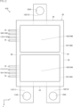
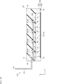
- FIG. 1 is a plan view showing a semiconductor device according to a first embodiment of the present disclosure
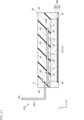
- FIG. FIG. 2 is a bottom view showing the semiconductor device according to the first embodiment of the present disclosure
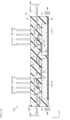
- FIG. FIG. 3 is a side view showing the semiconductor device according to the first embodiment of the present disclosure
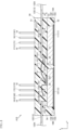
- FIG. 4 is a cross-sectional view taken along line IV-IV of FIG.
- FIG. 5 is a cross-sectional view along line VV of FIG.
- FIG. 6 is a cross-sectional view along line VI-VI of FIG.
- FIG. 7 is a cross-sectional view taken along line VII--VII of FIG.
- FIG. 8 is a cross-sectional view along line VIII-VIII of FIG.
- FIG. 9 is a cross-sectional view along line IX-IX in FIG.
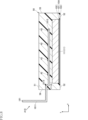
- FIG. 10 is a cross-sectional view taken along line XX of FIG. 1.
- FIG. 11 is a cross-sectional view along line XI-XI of FIG.
- FIG. 12 is a cross-sectional view showing a first modification of the semiconductor device according to the first embodiment of the present disclosure
- FIG. 13 is a cross-sectional view showing a second modification of the semiconductor device according to the first embodiment of the present disclosure
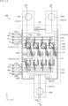
- FIG. 14 is a plan view showing a semiconductor device according to a second embodiment of the present disclosure
- FIG. 15 is a cross-sectional view along line XV-XV of FIG. 14.
- FIG. 16 is a cross-sectional view taken along line XVI--XVI of FIG. 14.
- a certain entity A is formed on a certain entity B” and “a certain entity A is formed on a certain entity B” mean “a certain entity A is formed on a certain entity B”. It includes "being directly formed in entity B” and “being formed in entity B while another entity is interposed between entity A and entity B”.
- ⁇ an entity A is placed on an entity B'' and ⁇ an entity A is located on an entity B'' mean ⁇ an entity A is located on an entity B.'' It includes "directly placed on B” and "some entity A is placed on an entity B while another entity is interposed between an entity A and an entity B.”
- ⁇ an object A is located on an object B'' means ⁇ an object A is adjacent to an object B and an object A is positioned on an object B. and "the thing A is positioned on the thing B while another thing is interposed between the thing A and the thing B".
- ⁇ an object A overlaps an object B when viewed in a certain direction'' means ⁇ an object A overlaps all of an object B'' and ⁇ an object A overlaps an object B.'' It includes "overlapping a part of a certain thing B".
- a certain surface A faces (one side or the other side of) direction B is not limited to the case where the angle of surface A with respect to direction B is 90 °, and the surface A Including when it is tilted against.
- First embodiment: 1 to 11 show a semiconductor device according to a first embodiment of the present disclosure.
- the semiconductor device A10 of this embodiment includes a first conductive member 11, a second conductive member 12, a third conductive member 13, a plurality of fourth conductive members 14, a plurality of fifth conductive members 15, and a plurality of first semiconductor elements 21. , a plurality of second semiconductor elements 22 and a sealing resin 50 .
- the semiconductor device A10 also includes leads 171, leads 172, leads 181, leads 182, a plurality of dummy terminals 19, a plurality of first wires 41, a plurality of second wires 42, a plurality of third wires 43 and a plurality of fourth wires.
- a wire 44 is provided.
- the semiconductor device A10 converts a DC power supply voltage applied to a first terminal 112 and a third terminal 132, which will be described later, into AC power using the plurality of first semiconductor elements 21 and the plurality of second semiconductor elements 22.
- the converted AC power is input to a power supply object such as a motor from a second terminal 122 which will be described later.
- the semiconductor device A10 forms part of a power conversion circuit such as an inverter. Note that the application and specific configuration of the semiconductor device according to the present disclosure are not limited at all.
- FIG. 1 is a plan view showing the semiconductor device A10.
- FIG. 2 is a bottom view showing the semiconductor device A10.
- FIG. 3 is a side view showing the semiconductor device A10.
- FIG. 4 is a cross-sectional view taken along line IV-IV of FIG.
- FIG. 5 is a cross-sectional view along line VV of FIG.
- FIG. 6 is a cross-sectional view along line VI-VI of FIG.
- FIG. 7 is a cross-sectional view taken along line VII--VII of FIG.
- FIG. 8 is a cross-sectional view along line VIII-VIII of FIG.
- FIG. 9 is a cross-sectional view along line IX-IX in FIG. 10 is a cross-sectional view taken along line XX of FIG. 1.
- FIG. 11 is a cross-sectional view along line XI-XI of FIG.
- the z-direction is an example of the "thickness direction.”
- the x-direction is an example of a "first direction”
- the y-direction is an example of a "second direction”.
- the encapsulating resin 50 is indicated by imaginary lines.
- the first conductive member 11 includes a first base material 111 , a first terminal 112 and a first pillow material 113 .
- the first base material 111 is made of a conductive material and contains Cu (copper), for example.
- the first base material 111 is arranged on one side in the x direction.
- the first base material 111 has a first major surface 111A.
- the first major surface 111A faces one side in the z direction. In the illustrated example, the first main surface 111A is a flat surface.
- the first terminal 112 protrudes to one side in the x direction and has a portion exposed from the sealing resin 50, as shown in FIGS.
- the first terminal 112 is arranged at a position shifted to one side in the x direction with respect to the first base material 111 .
- the first terminal 112 is arranged at a position shifted to the other side in the y direction with respect to the first base material 111 .
- the first terminal 112 is arranged on one side in the z direction with respect to the first main surface 111A and is separated from the first base material 111 .
- the first terminal 112 overlaps the first main surface 111A when viewed in the z direction.
- the composition of the first terminal 112 contains Cu (copper).
- the first terminal 112 is provided with a first attachment hole 112A.
- the first attachment hole 112A penetrates the first terminal 112 in the z direction.
- the first pillow material 113 is interposed between the first base material 111 and the first terminal 112, as shown in FIGS.
- the composition of the first pillow material 113 contains Cu (copper).
- the first pillow material 113 is conductively joined to the first main surface 111A of the first base material 111 and the first terminals 112 .
- the method of conductive joining is not limited at all, and a method using a conductive joining material such as solder, a method such as welding, or the like may be appropriately adopted.
- the first base material 111 is supported by the supporting member 10A.
- the support member 10A is located on the opposite side of the first base material 111 from the first major surface 111A.
- the specific configuration of the support member 10A is not limited at all, and in the present embodiment, the support member 10A is composed of a DBC (Direct Bonded Copper) substrate.
- the support member 10A includes an insulating layer 101, a support layer 102 and a heat dissipation layer 103. As shown in FIG.
- the support member 10A is covered with a sealing resin 50 except for a part of the heat dissipation layer 103. As shown in FIG.
- the insulating layer 101 includes a portion located between the support layer 102 and the heat dissipation layer 103 in the z direction.
- the insulating layer 101 is made of a material with higher thermal conductivity.
- Insulating layer 101 is made of, for example, ceramics containing aluminum nitride (AlN). The thickness of the insulating layer 101 is thinner than the thickness of the first base material 111 .
- the support layer 102 is located between the insulating layer 101 and the first base material 111 in the z direction.
- the composition of the support layer 102 includes copper (Cu).
- the support layer 102 is surrounded by the periphery of the insulating layer 101 when viewed in the z-direction.
- the support layer 102 is bonded to the first base material 111 via solder, for example.
- the heat dissipation layer 103 is located on the opposite side of the support layer 102 with respect to the insulating layer 101 in the z direction. A portion of the heat dissipation layer 103 is exposed from the sealing resin 50 .
- a heat sink (not shown) is bonded to the heat dissipation layer 103 when the semiconductor device A10 is used.
- the composition of the heat dissipation layer 103 contains copper.
- the heat dissipation layer 103 is surrounded by the periphery of the insulating layer 101 when viewed in the z-direction.
- the second conductive member 12 includes a second base material 121 , second terminals 122 and a second pillow material 123 .
- the second base material 121 is made of a conductive material and contains Cu (copper), for example.
- the second base material 121 is arranged on the other side in the x direction.
- the second base material 121 has a second major surface 121A.
- the second main surface 121A faces one side in the z direction. In the illustrated example, the second major surface 121A is a flat surface.
- the second terminal 122 protrudes to the other side in the x direction and has a portion exposed from the sealing resin 50.
- the second terminal 122 is arranged at a position shifted to the other side in the x direction with respect to the second substrate 121 .
- the center position of the second terminal 122 in the y-direction substantially coincides with the center position of the second base material 121 in the y-direction.
- the second terminal 122 is arranged on one side in the z direction with respect to the second main surface 121A and is separated from the second base material 121 .
- the second terminal 122 overlaps the second main surface 121A when viewed in the z direction.
- the composition of the second terminal 122 contains Cu (copper).
- the second terminal 122 is provided with a second mounting hole 122A.
- the second attachment hole 122A penetrates the second terminal 122 in the z direction.
- the second pillow material 123 is interposed between the second base material 121 and the second terminal 122, as shown in FIGS.
- the composition of the second pillow material 123 contains Cu (copper).
- the second pillow material 123 is conductively joined to the second main surface 121A of the second base material 121 and the second terminals 122 .
- the method of conductive joining is not limited at all, and a method using a conductive joining material such as solder, a method such as welding, or the like may be appropriately adopted.
- the second base material 121 is supported by the supporting member 10B.
- the support member 10B is located on the opposite side of the second base material 121 from the second main surface 121A.
- the specific configuration of the support member 10A is not limited at all, and in the present embodiment, the configuration is the same as that of the support member 10A, so the description thereof will be omitted.
- First semiconductor element 21 The plurality of first semiconductor elements 21 are bonded to the first main surface 111A of the first base material 111, as shown in FIGS. 1 and 4 to 7. FIG. All of the plurality of first semiconductor elements 21 are the same element.
- the plurality of first semiconductor elements 21 are, for example, MOSFETs (Metal-Oxide-Semiconductor Field-Effect Transistors).
- the plurality of first semiconductor elements 21 may be field effect transistors including MISFETs (Metal-Insulator-Semiconductor Field-Effect Transistors) or bipolar transistors such as IGBTs (Insulated Gate Bipolar Transistors).
- the first semiconductor element 21 may be a diode.
- the plurality of first semiconductor elements 21 are n-channel type vertical MOSFETs.
- the plurality of first semiconductor elements 21 includes compound semiconductor substrates.
- the composition of the compound semiconductor substrate includes silicon carbide (SiC).
- the plurality of first semiconductor elements 21 are arranged along the y direction.
- the first semiconductor element 21 has a first back surface electrode 211 , a first main surface electrode 212 and a first gate electrode 213 .
- the first rear surface electrode 211 faces the first main surface 111A of the first base material 111 .
- a current corresponding to power before being converted by the first semiconductor element 21 flows through the first back electrode 211 . That is, the first rear surface electrode 211 corresponds to the drain electrode of the first semiconductor element 21 .
- the first rear surface electrode 211 is conductively joined to the first main surface 111A via the conductive joining layer 29 . Therefore, the first rear surface electrodes 211 of the plurality of first semiconductor elements 21 are electrically connected to the first conductive member 11 .
- Conductive bonding layer 29 is, for example, solder. Alternatively, the conductive bonding layer 29 may be a sintered metal containing silver or the like.
- the first main surface electrode 212 is located on one side opposite to the first rear surface electrode 211 in the z direction. A current corresponding to the power converted by the first semiconductor element 21 flows through the first main surface electrode 212 . That is, the first principal surface electrode 212 corresponds to the source electrode of the first semiconductor element 21 .
- the first gate electrode 213 is located on the same side (one side) as the first principal surface electrode 212 in the z direction. A gate voltage for driving the first semiconductor element 21 is applied to the first gate electrode 213 . As shown in FIG. 3, the area of the first gate electrode 213 is smaller than the area of the first main surface electrode 212 when viewed in the direction.
- Second semiconductor element 22 The plurality of second semiconductor elements 22 are bonded to the second main surface 121A of the second base material 121, as shown in FIGS. 1 and 4-6.
- the multiple second semiconductor elements 22 are the same elements as the multiple first semiconductor elements 21 . Therefore, the plurality of second semiconductor elements 22 are n-channel type vertical MOSFETs.
- the plurality of second semiconductor elements 22 may be field effect transistors including MISFETs (Metal-Insulator-Semiconductor Field-Effect Transistors) or bipolar transistors such as IGBTs (Insulated Gate Bipolar Transistors).
- MISFETs Metal-Insulator-Semiconductor Field-Effect Transistors
- IGBTs Insulated Gate Bipolar Transistors
- the second semiconductor element 22 may be a diode.
- the plurality of second semiconductor elements 22 are n-channel type vertical MOSFETs.
- the plurality of second semiconductor elements 22 include compound semiconductor substrates.
- the composition of the compound semiconductor substrate includes silicon carbide (SiC).
- a plurality of second semiconductor elements 22 are arranged along the y direction.
- the plurality of second semiconductor elements 22 have second rear surface electrodes 221 , second main surface electrodes 222 and second gate electrodes 223 .
- the second back surface electrode 221 faces the second main surface 121A of the second base material 121 .
- a current corresponding to the power before being converted by the second semiconductor element 22 flows through the second back electrode 221 . That is, the second backside electrode 221 corresponds to the drain electrode of the second semiconductor element 22 .
- the second back surface electrode 221 is conductively joined to the second main surface 121A via the conductive joining layer 29 . Therefore, the second back electrodes 221 of the plurality of second semiconductor elements 22 are electrically connected to the second conductive member 12 .
- the second main surface electrode 222 is located on one side opposite to the second rear surface electrode 221 in the z direction. A current corresponding to the power converted by the second semiconductor element 22 flows through the second principal surface electrode 222 . That is, the second principal surface electrode 222 corresponds to the source electrode of the second semiconductor element 22 .
- the second gate electrode 223 is located on the same side (one side) as the second principal surface electrode 222 in the z direction. A gate voltage for driving the second semiconductor element 22 is applied to the second gate electrode 223 .
- the area of the second gate electrode 223 is smaller than the area of the second main surface electrode 222 when viewed in the z direction.
- the third conductive member 13 includes an extension portion 131 and a third terminal 132, as shown in FIGS. 1, 2 and 4-7.
- the third conductive member 13 is made of a conductive material, such as Cu (copper).
- the third terminal 132 has a portion protruding from the sealing resin 50 to one side in the z direction.
- the third terminal 132 is located on one side of the first terminal 112 in the y direction.
- the third terminal 132 is arranged at a position shifted to one side in the x direction with respect to the second base member 121 .
- the third terminal 132 is arranged on one side in the z direction with respect to the first main surface 111A and is separated from the first base material 111 .
- the third terminal 132 overlaps the first main surface 111A when viewed in the z direction.
- the third terminal 132 is provided with a third attachment hole 132A.
- the third attachment hole 132A penetrates the third terminal 132 in the z direction.
- the extending portion 131 extends from the third terminal 132 to the other side in the x direction and is covered with the sealing resin 50 .
- the extending portion 131 of this embodiment includes a first portion 1311 , a second portion 1312 and a third portion 1313 .
- the first portion 1311 has a distance z1 from the first main surface 111A in the z direction smaller than a distance z0 from the first main surface 111A to the third terminal 132 in the z direction. is.
- the size of the distance z1 is, for example, 0.1 mm or more.
- the first portion 1311 is positioned between the plurality of first semiconductor elements 21 and the plurality of second semiconductor elements 22 in the x-direction, as shown in FIGS.
- the distance z1 is greater than the distance z2 from the first main surface 111A in the z direction to one side end of the first semiconductor element 21 in the z direction.
- the distance z2 is approximately 0.5 mm
- the distance z1 is approximately 0.8 mm to 1.2 mm.
- the shape of the first part 1311 is not limited at all, and in the present embodiment, it has a shape extending in the y direction, for example, a flat belt shape.
- the first portion 1311 overlaps the first main surface 111A (first base material 111) when viewed in the z direction.
- the other x-direction edge of the first portion 1311 is located on one side in the x-direction from the other x-direction edge of the first main surface 111A.
- the second part 1312 is connected to the third terminal 132.
- the second portion 1312 extends along the x direction from the third terminal 132 to the other side in the x direction.
- the shape of the second portion 1312 is not limited at all, and is, for example, a flat belt shape.
- the distance from the first main surface 111A to the second portion 1312 in the z direction is the same as the distance z0.
- the second part 1312 is positioned on one side in the y direction (on the right side in FIG. 1) with respect to the plurality of first semiconductor elements 21 .
- the other edge of the second portion 1312 in the x direction is located on the other side in the x direction of the one edge of the first semiconductor element 21 in the x direction.
- the third part 1313 is interposed between the first part 1311 and the second part 1312 .
- the extending portion 131 has a bent shape when viewed in the y direction.
- the third portion 1313 is part of the one side edge in the x direction of the first portion 1311 and is connected to a portion near the one side edge in the y direction.
- Fourth conductive member 14 As shown in FIGS. 1, 5 and 7, the plurality of fourth conductive members 14 electrically connect the plurality of first semiconductor elements 21 and the second conductive members 12 individually. More specifically, the fourth conductive member 14 is connected to the first principal surface electrode 212 of the first semiconductor element 21 .
- a specific configuration of the fourth conductive member 14 is not limited at all, and is, for example, a wire or ribbon containing a metal material. Metal materials include, for example, Cu (copper), Al (aluminum), and alloys thereof.
- the fourth conductive member 14 of this example is a wire containing Cu (copper).
- the number of fourth conductive members 14 is not limited at all, and in the illustrated example, two fourth conductive members 14 are connected to the first principal surface electrode 212 of one first semiconductor element 21 .
- the fourth conductive member 14 straddles the first portion 1311 on one side in the z direction. That is, the fourth conductive member 14 has a portion located away from the first portion 1311 on one side in the z direction. In the illustrated example, the fourth conductive member 14 has a curved shape that straddles the first portion 1311 on one side in the z direction.
- the plurality of fifth conductive members 15 electrically connect the plurality of first semiconductor elements 21 and the third conductive members 13 individually. More specifically, the fifth conductive member 15 is connected to the second principal surface electrode 222 of the second semiconductor element 22 .
- the specific configuration of the plurality of fifth conductive members 15 is not limited at all, and may be, for example, wires and ribbons containing metal material, or members made of plate material.
- the fifth conductive member 15 may be configured by a member separate from the third conductive member 13 , or may be formed integrally with the third conductive member 13 . In this embodiment, the fifth conductive member 15 is separate from the third conductive member 13, and is a wire containing Cu (copper), for example.
- the number of fifth conductive members 15 is not limited at all, and in the illustrated example, two fifth conductive members 15 are connected to the second principal surface electrode 222 of one second semiconductor element 22 .
- the plurality of fifth conductive members 15 are connected to the first portion 1311 of the extension portion 131 of the third conductive member 13 . As shown in FIG. 1, the plurality of fourth conductive members 14 and the plurality of fifth conductive members 15 are alternately arranged in the y direction. In the illustrated example, two fourth conductive members 14 and two fifth conductive members 15 are alternately arranged.
- the lead 171 includes a first gate terminal 1711, a first gate wiring portion 1712 and a stepped portion 1713, as shown in FIGS.
- the lead 171 is a so-called lead member and contains Cu (copper) in its composition, for example.
- the first gate terminal 1711 is positioned outside the sealing resin 50 and functions as a gate terminal for operating the plurality of first semiconductor elements 21 of the semiconductor device A10.
- the first gate wiring portion 1712 is located on one side in the x direction with respect to the plurality of first semiconductor elements 21, and is separated from the first main surface 111A of the first substrate 111 on one side in the z direction. .
- the first gate wiring portion 1712 has a shape extending in the y direction.
- the distance from the first main surface 111A to the first gate wiring portion 1712 in the z direction is smaller than the distance from the first main surface 111A to the first gate terminal 1711 in the z direction.
- the first gate wiring portion 1712 and the first gate electrodes 213 of the plurality of first semiconductor elements 21 are individually conductively connected by the plurality of first wires 41 .
- the first wire 41 is a wire containing Au (gold), for example.
- the step portion 1713 is positioned between the first gate terminal 1711 and the first gate wiring portion 1712 . By having the step portion 1713, the lead 171 has a bent shape when viewed in the x direction.
- the lead 181 includes a first detection terminal 1811, a first detection wiring portion 1812 and a stepped portion 1813, as shown in FIGS.
- the lead 181 is a so-called lead member and contains, for example, Cu (copper) in its composition.
- the first detection terminal 1811 is positioned outside the sealing resin 50 and functions as a detection terminal for detecting the operating state of the plurality of first semiconductor elements 21 of the semiconductor device A10.
- the first detection wiring portion 1812 is positioned on one side in the x direction with respect to the first gate wiring portion 1712 and is separated from the first main surface 111A of the first substrate 111 on one side in the z direction.
- the first detection wiring portion 1812 has a shape extending in the y direction.
- the distance from the first main surface 111A to the first detection wiring portion 1812 in the z direction is smaller than the distance from the first main surface 111A to the first detection terminal 1811 in the z direction.
- the first detection wiring portion 1812 and the first main surface electrodes 212 of the plurality of first semiconductor elements 21 are individually conductively connected by the plurality of second wires 42 .
- the second wire 42 is a wire containing Au (gold), for example.
- the step portion 1813 is positioned between the first detection terminal 1811 and the first detection wiring portion 1812 . By having the step portion 1813, the lead 181 has a bent shape when viewed in the x direction.
- the lead 172 includes a second gate terminal 1721, a second gate wiring portion 1722 and a stepped portion 1723, as shown in FIGS.
- the lead 172 is a so-called lead member and contains, for example, Cu (copper) in its composition.
- the second gate terminal 1721 is located outside the sealing resin 50 and functions as a gate terminal for operating the plurality of second semiconductor elements 22 of the semiconductor device A10.
- the second gate wiring portion 1722 is located on the other side in the x direction with respect to the plurality of second semiconductor elements 22, and is separated from the first main surface 111A of the first substrate 111 to one side in the z direction. .
- the second gate wiring portion 1722 has a shape extending in the y direction.
- the distance from the first main surface 111A to the second gate wiring portion 1722 in the z direction is smaller than the distance from the first main surface 111A to the second gate terminal 1721 in the z direction.
- the second gate wiring portion 1722 and the second gate electrodes 223 of the plurality of second semiconductor elements 22 are individually conductively connected by the plurality of third wires 43 .
- the third wire 43 is a wire containing Au (gold), for example.
- the step portion 1723 is positioned between the second gate terminal 1721 and the second gate wiring portion 1722 . By having the step portion 1723, the lead 172 has a bent shape when viewed in the x direction.
- the lead 182 includes a second detection terminal 1821, a second detection wiring portion 1822 and a stepped portion 1823, as shown in FIGS.
- the lead 182 is a so-called lead member and contains, for example, Cu (copper) in its composition.
- the second detection terminal 1821 is positioned outside the sealing resin 50 and functions as a detection terminal for detecting the operating state of the plurality of second semiconductor elements 22 of the semiconductor device A10.
- the second detection wiring portion 1822 is located on the other side in the x direction with respect to the second gate wiring portion 1722 and is separated from the first main surface 111A of the first base material 111 to one side in the z direction.
- the second detection wiring portion 1822 has a shape extending in the y direction.
- the distance from the first main surface 111A to the second detection wiring portion 1822 in the z direction is smaller than the distance from the first main surface 111A to the second detection terminal 1821 in the z direction.
- the second detection wiring portion 1822 and the second main surface electrodes 222 of the plurality of second semiconductor elements 22 are electrically connected individually by the plurality of fourth wires 44 .
- the fourth wire 44 is a wire containing Au (gold), for example.
- the step portion 1823 is positioned between the second detection terminal 1821 and the second detection wiring portion 1822 . By having the step portion 1823, the lead 182 has a bent shape when viewed in the x direction.
- Dummy terminal 19 The semiconductor device A10 further includes four dummy terminals 19, as shown in FIGS. Two of the four dummy terminals 19 are arranged on both sides of the first gate terminal 1711 and the first detection terminal 1811 in the x direction. The remaining two dummy terminals 19 are arranged on both sides of the second gate terminal 1721 and the second detection terminal 1821 in the x direction. Dummy terminal 19 is a metal lead made of a material containing copper or a copper alloy. A portion of each of the plurality of dummy terminals 19 is covered with a sealing resin. Portions of the plurality of dummy terminals 19 standing up in the z-direction are exposed from the sealing resin 50 .
- the sealing resin 50 includes a first base material 111, a second base material 121, a plurality of fourth conductive members 14, a plurality of fifth conductive members 15, and a plurality of first semiconductor elements. 21 and a plurality of second semiconductor elements 22 . Further, the sealing resin 50 is partially formed of the first terminal 112, the second terminal 122, and the third terminal 132, the extending portion 131, the first gate wiring portion 1712, the first detection wiring portion 1812, and the second gate wiring. It covers the portion 1722 and the second detection wiring portion 1822 .
- the sealing resin 50 has electrical insulation. Sealing resin 50 is made of a material containing, for example, black epoxy resin.
- the sealing resin 50 has a top surface 51 , a bottom surface 52 , a first side surface 53 , a second side surface 54 , a third side surface and a fourth side surface 56 .
- the top surface 51 is a surface facing one side in the z direction.
- the bottom surface 52 is a surface facing the other side in the z direction.
- the first side surface 53 is a surface facing one side in the x direction.
- a first terminal 112 and a third terminal 132 protrude from the first side surface 53 .
- the second side surface 54 is a surface facing the other side in the x direction.
- a second terminal 122 protrudes from the second side surface 54 .
- the third side surface 55 is a surface facing one side in the y direction.
- the fourth side surface 56 is a surface facing the other side in the y direction.
- a first gate terminal 1711 , a first detection terminal 1811 , a second gate terminal 1721 , a second detection terminal 1821 and a plurality of dummy terminals 19 protrude from the fourth side surface 56 .
- the first portion 1311 is positioned between the plurality of first semiconductor elements 21 and the plurality of second semiconductor elements 22 in the z-direction. Also, the distance z1 from the first main surface 111A to the first portion 1311 in the z direction is smaller than the distance z0 from the first main surface 111A to the third terminal 132 in the z direction. Therefore, while avoiding contact or short-circuiting between the fourth conductive member 14 and the first portion 1311, the fourth conductive member 14 straddling the first portion 1311 on one side in the z-direction can move from the first main surface 111A to the z-direction. can be reduced. Therefore, the size of the semiconductor device A10 can be reduced while properly operating the semiconductor device A10.
- the first part 1311 has a shape extending in the y direction. As a result, it is possible to secure a wider area for connecting the plurality of fifth conductive members 15 , and to avoid improper conduction between the fourth conductive member 14 and the fifth conductive member 15 .
- the distance z1 from the first principal surface 111A to the first portion 1311 in the z direction is the distance from the first principal surface 111A to one end of the first semiconductor element 21 in the z direction. greater than z2. As a result, for example, it is possible to prevent the first portion 1311 from unduly interfering with the plurality of first semiconductor elements 21 .
- the second portion 1312 is located on one side of the plurality of first semiconductor elements 21 in the y direction. Therefore, it is not necessary to secure a space for arranging the second part 1312 between the adjacent first semiconductor elements 21 . Therefore, it is preferable for miniaturization of the semiconductor device A10.
- the extension part 131 has a bent shape with a third part 1313 . Accordingly, it is possible to prevent the extending portion 131 from increasing in size while arranging the first portion 1311 and the second portion 1312 at different positions in the z-direction.
- the plurality of fifth conductive members 15 are separate from the extending portion 131 (first portion 1311) of the third conductive member 13, and are made of wires in this embodiment. With such a configuration, it is possible to reduce the width (diameter) of the fifth conductive member 15 . In addition, it is possible to connect to desired portions of the first portion 1311 and the second main surface electrode 222 of the second semiconductor element 22, which is preferable for suppressing interference with the fourth conductive member 14 and short circuit, for example.
- the first portion 1311 overlaps the first main surface 111A when viewed in the z direction. Thereby, the space for connecting the plurality of fourth conductive members 14 to the second main surface 121A can be more easily secured.
- the leads 171 , 181 , 172 and 182 each have a first gate wiring portion 1712 , a first detection wiring portion 1812 , a second gate wiring portion 1722 and a second detection wiring portion 1822 .
- the first gate wiring portion 1712 is electrically connected to the first gate electrodes 213 of the plurality of first semiconductor elements 21 through the plurality of first wires 41 .
- the first detection wiring portion 1812 is electrically connected to the first principal surface electrodes 212 of the plurality of first semiconductor elements 21 through the plurality of second wires 42 .
- the second gate wiring portion 1722 is electrically connected to the second gate electrodes 223 of the plurality of second semiconductor elements 22 through the plurality of third wires 43 .
- the second detection wiring portion 1822 is electrically connected to the second principal surface electrodes 222 of the plurality of second semiconductor elements 22 through the plurality of fourth wires 44 .
- the first gate wiring portion 1712, the first detection wiring portion 1812, the second gate wiring portion 1722, and the second detection wiring portion 1822 are parts of the lead 171, the lead 181, the lead 172, and the lead 182, and 111 and away from the second substrate 121 in the z-direction. Accordingly, functions similar to those of the first gate wiring portion 1712, the first detection wiring portion 1812, the second gate wiring portion 1722, and the second detection wiring portion 1822 can be provided on the first main surface 111A and the second main surface 121A, for example. There is no need to form a wiring portion that fulfills the requirements. Therefore, complication of the structure of the semiconductor device A10 can be suppressed.
- FIG. 12 shows a first modification of the semiconductor device A10.
- the semiconductor device A11 of this modified example differs from the example described above in the relationship between the first part 1311 and the first semiconductor element 21 .
- the distance z1 from the first main surface 111A to the first portion 1311 in the z direction is greater than the distance z2 from the first main surface 111A to one side end of the first semiconductor element 21 in the z direction. is also small.
- the distance z2 is approximately 0.5 mm
- the distance z1 is approximately 0.1 mm to 0.3 mm.
- the semiconductor device A11 can be downsized while properly operating the semiconductor device A11. Further, according to this modification, it is possible to further reduce the distance from the first main surface 111A in the z direction to the one side end of the fourth conductive member 14 in the z direction. This is advantageous for miniaturization of the semiconductor device A11.
- FIG. 13 shows a second modification of the semiconductor device A10.
- the relationship between the first part 1311 and the first base material 111 and the second base material 121 is different from the example described above.
- the first portion 1311 overlaps the second main surface 121A (second base material 121) when viewed in the z direction. Further, in the illustrated example, one edge of the first portion 1311 in the x direction overlaps with one edge of the second principal surface 121A in the x direction, or one edge of the second principal surface 121A in the x direction overlaps with the edge of the second principal surface 121A in the x direction. It is positioned on the other side in the x-direction from the side edge.
- the first portion 1311 may overlap the first main surface 111A or the second main surface 121A when viewed in the z direction. good too.
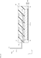
- FIG. 14 to 16 show a semiconductor device according to a second embodiment of the present disclosure.
- the semiconductor device A20 of this embodiment differs from the embodiment described above in the configuration of the third conductive member 13 and the plurality of fifth conductive members 15 .
- FIG. 14 is a plan view showing the semiconductor device A20.
- 15 is a cross-sectional view along line XV-XV of FIG. 14.
- FIG. 16 is a cross-sectional view taken along line XVI--XVI of FIG. 14.
- the plurality of fifth conductive members 15 are formed integrally with the third conductive member 13. More specifically, the plurality of fifth conductive members 15 have a shape extending from the third conductive member 13 to the other side in the x direction. The multiple fifth conductive members 15 are arranged in the y direction. The distance from the first main surface 111A and the second main surface 121A to the plurality of fifth conductive members 15 in the z direction is the same as the distance from the first main surface 111A to the first portion 1311 in the z direction.
- the fifth conductive member 15 is joined to the second main surface electrode 222 of the second semiconductor element 22 by a conductive joining layer 28, for example.
- the conductive bonding layer 28 is solder, for example.
- the conductive bonding layer 28 may be a sintered metal containing silver or the like.
- the semiconductor device A20 can be miniaturized while properly operating the semiconductor device A20.
- the fifth conductive member 15 may be formed integrally with the first portion 1311 of the third conductive member 13 .
- the resistance can be further reduced by integrally forming the fifth conductive member 15 with the third conductive member 13 by a so-called lead member.
- the semiconductor device according to the present disclosure is not limited to the above-described embodiments.
- the specific configuration of each part of the semiconductor device according to the present disclosure can be changed in various ways.
- the present disclosure includes embodiments set forth in the following appendices.
- Appendix 1 a first conductive member having a first main surface facing one side in the thickness direction and arranged on one side in a first direction orthogonal to the thickness direction; a second conductive member having a second main surface facing one side in the thickness direction and arranged on the other side in the first direction; a first semiconductor element electrically connected to the first main surface; a second semiconductor element electrically connected to the second main surface; a third conductive member; a fourth conductive member that electrically connects the first semiconductor element and the second conductive member; a fifth conductive member that electrically connects the second semiconductor element and the third conductive member; covering parts of each of the first conductive member, the second conductive member and the third conductive member, and the first semiconductor element, the second semiconductor element, the fourth conductive
- Appendix 2 The semiconductor device according to appendix 1, wherein the first portion has a shape extending in a second direction orthogonal to the thickness direction and the first direction.
- Appendix 3. comprising a plurality of the first semiconductor elements arranged in the second direction;
- Appendix 4. comprising a plurality of the second semiconductor elements arranged in the second direction;
- the first conductive member includes a first terminal that protrudes from the sealing resin to one side in the first direction and is positioned on the other side in the second direction with respect to the third terminal.
- Appendix 14. 14 The semiconductor device according to appendix 13, wherein the second conductive member includes a second terminal projecting from the sealing resin to the other side in the first direction.
- Appendix 15. The semiconductor device according to any one of Appendixes 4 to 14, wherein the first portion overlaps the first main surface when viewed in the thickness direction.
- Appendix 17. 17. The semiconductor device according to any one of appendices 1 to 16, wherein the first semiconductor element and the second semiconductor element are switching elements.
- A10, A11, A12, A20 semiconductor devices 10A, 10B: support member 11: first conductive member 12: second conductive member 13: third conductive member 14: fourth conductive member 15: fifth conductive member 19: dummy terminal 21: First semiconductor element 22: Second semiconductor element 28: Conductive bonding layer 29: Conductive bonding layer 41: First wire 42: Second wire 43: Third wire 44: Fourth wire 50: Sealing resin 51: Top Surface 52: Bottom surface 53: First side surface 54: Second side surface 55: Third side surface 56: Fourth side surface 101: Insulating layer 102: Support layer 103: Heat dissipation layer 111: First base material 111A: First main surface 112: First Terminal 112A: First Mounting Hole 113: First Pillow 121: Second Base Material 121A: Second Main Surface 122: Second Terminal 122A: Second Mounting Hole 123: Second Pillow 131: Extension 132 : third terminal 132A: third mounting holes 171, 172, 181, 182: lead 211: first rear surface electrode 212:
Landscapes
- Structures Or Materials For Encapsulating Or Coating Semiconductor Devices Or Solid State Devices (AREA)
Priority Applications (4)
| Application Number | Priority Date | Filing Date | Title |
|---|---|---|---|
| DE112023000813.2T DE112023000813T5 (de) | 2022-02-04 | 2023-01-23 | Halbleitervorrichtung |
| JP2023578482A JPWO2023149257A1 (https=) | 2022-02-04 | 2023-01-23 | |
| CN202380019178.8A CN118633159A (zh) | 2022-02-04 | 2023-01-23 | 半导体装置 |
| US18/782,758 US20240379510A1 (en) | 2022-02-04 | 2024-07-24 | Circuit component, electronic device and method for producing circuit component |
Applications Claiming Priority (2)
| Application Number | Priority Date | Filing Date | Title |
|---|---|---|---|
| JP2022016239 | 2022-02-04 | ||
| JP2022-016239 | 2022-02-04 |
Related Child Applications (1)
| Application Number | Title | Priority Date | Filing Date |
|---|---|---|---|
| US18/782,758 Continuation US20240379510A1 (en) | 2022-02-04 | 2024-07-24 | Circuit component, electronic device and method for producing circuit component |
Publications (1)
| Publication Number | Publication Date |
|---|---|
| WO2023149257A1 true WO2023149257A1 (ja) | 2023-08-10 |
Family
ID=87552137
Family Applications (1)
| Application Number | Title | Priority Date | Filing Date |
|---|---|---|---|
| PCT/JP2023/001891 Ceased WO2023149257A1 (ja) | 2022-02-04 | 2023-01-23 | 半導体装置 |
Country Status (5)
| Country | Link |
|---|---|
| US (1) | US20240379510A1 (https=) |
| JP (1) | JPWO2023149257A1 (https=) |
| CN (1) | CN118633159A (https=) |
| DE (1) | DE112023000813T5 (https=) |
| WO (1) | WO2023149257A1 (https=) |
Cited By (1)
| Publication number | Priority date | Publication date | Assignee | Title |
|---|---|---|---|---|
| WO2025247764A1 (de) * | 2024-05-28 | 2025-12-04 | Robert Bosch Gmbh | Einzelschalter leistungsmodul |
Citations (2)
| Publication number | Priority date | Publication date | Assignee | Title |
|---|---|---|---|---|
| JP2020504459A (ja) * | 2017-01-13 | 2020-02-06 | クリー ファイエットヴィル インコーポレイテッド | パワーデバイスを並列接続するための低インダクタンスおよび高速スイッチングを有するハイパワー多層モジュール |
| WO2021176996A1 (ja) * | 2020-03-04 | 2021-09-10 | ローム株式会社 | 半導体装置および半導体装置の製造方法 |
Family Cites Families (1)
| Publication number | Priority date | Publication date | Assignee | Title |
|---|---|---|---|---|
| US11211312B2 (en) | 2017-11-20 | 2021-12-28 | Rohm Co., Ltd. | Semiconductor device |
-
2023
- 2023-01-23 JP JP2023578482A patent/JPWO2023149257A1/ja active Pending
- 2023-01-23 CN CN202380019178.8A patent/CN118633159A/zh active Pending
- 2023-01-23 WO PCT/JP2023/001891 patent/WO2023149257A1/ja not_active Ceased
- 2023-01-23 DE DE112023000813.2T patent/DE112023000813T5/de active Pending
-
2024
- 2024-07-24 US US18/782,758 patent/US20240379510A1/en active Pending
Patent Citations (2)
| Publication number | Priority date | Publication date | Assignee | Title |
|---|---|---|---|---|
| JP2020504459A (ja) * | 2017-01-13 | 2020-02-06 | クリー ファイエットヴィル インコーポレイテッド | パワーデバイスを並列接続するための低インダクタンスおよび高速スイッチングを有するハイパワー多層モジュール |
| WO2021176996A1 (ja) * | 2020-03-04 | 2021-09-10 | ローム株式会社 | 半導体装置および半導体装置の製造方法 |
Cited By (1)
| Publication number | Priority date | Publication date | Assignee | Title |
|---|---|---|---|---|
| WO2025247764A1 (de) * | 2024-05-28 | 2025-12-04 | Robert Bosch Gmbh | Einzelschalter leistungsmodul |
Also Published As
| Publication number | Publication date |
|---|---|
| JPWO2023149257A1 (https=) | 2023-08-10 |
| DE112023000813T5 (de) | 2024-11-14 |
| CN118633159A (zh) | 2024-09-10 |
| US20240379510A1 (en) | 2024-11-14 |
Similar Documents
| Publication | Publication Date | Title |
|---|---|---|
| US20240404977A1 (en) | Semiconductor device and semiconductor module | |
| WO2023112662A1 (ja) | 半導体モジュールおよび半導体装置 | |
| US20240379510A1 (en) | Circuit component, electronic device and method for producing circuit component | |
| JP7545845B2 (ja) | 半導体装置 | |
| JP2023088628A (ja) | 半導体装置 | |
| JPWO2020149225A1 (ja) | 半導体装置 | |
| US20240030080A1 (en) | Semiconductor device | |
| WO2024029336A1 (ja) | 半導体装置 | |
| WO2023100663A1 (ja) | 半導体装置 | |
| WO2024075589A1 (ja) | 半導体装置 | |
| WO2024106219A1 (ja) | 半導体装置 | |
| US20240047315A1 (en) | Semiconductor device | |
| US20240203849A1 (en) | Semiconductor device and mounting structure for semiconductor device | |
| WO2023120353A1 (ja) | 半導体装置 | |
| WO2022259825A1 (ja) | 半導体装置 | |
| WO2024111367A1 (ja) | 半導体装置 | |
| WO2024029385A1 (ja) | 半導体装置 | |
| WO2023120185A1 (ja) | 半導体装置 | |
| WO2024241819A1 (ja) | 電子装置 | |
| WO2024018795A1 (ja) | 半導体装置 | |
| WO2023224113A1 (ja) | 半導体装置 | |
| WO2023199808A1 (ja) | 半導体装置 | |
| WO2024128062A1 (ja) | 半導体装置 | |
| WO2024116743A1 (ja) | 半導体装置 | |
| WO2024018851A1 (ja) | 半導体装置 |
Legal Events
| Date | Code | Title | Description |
|---|---|---|---|
| 121 | Ep: the epo has been informed by wipo that ep was designated in this application |
Ref document number: 23749573 Country of ref document: EP Kind code of ref document: A1 |
|
| WWE | Wipo information: entry into national phase |
Ref document number: 2023578482 Country of ref document: JP |
|
| WWE | Wipo information: entry into national phase |
Ref document number: 202380019178.8 Country of ref document: CN |
|
| WWE | Wipo information: entry into national phase |
Ref document number: 112023000813 Country of ref document: DE |
|
| 122 | Ep: pct application non-entry in european phase |
Ref document number: 23749573 Country of ref document: EP Kind code of ref document: A1 |