WO2023145015A1 - Dispositif d'inspection et procédé d'inspection de qualité de film - Google Patents
Dispositif d'inspection et procédé d'inspection de qualité de film Download PDFInfo
- Publication number
- WO2023145015A1 WO2023145015A1 PCT/JP2022/003391 JP2022003391W WO2023145015A1 WO 2023145015 A1 WO2023145015 A1 WO 2023145015A1 JP 2022003391 W JP2022003391 W JP 2022003391W WO 2023145015 A1 WO2023145015 A1 WO 2023145015A1
- Authority
- WO
- WIPO (PCT)
- Prior art keywords
- sample
- light
- signal
- charged particle
- film quality
- Prior art date
Links
- 238000007689 inspection Methods 0.000 title claims abstract description 87
- 238000000034 method Methods 0.000 title claims description 8
- 238000001514 detection method Methods 0.000 claims abstract description 54
- 239000002245 particle Substances 0.000 claims abstract description 54
- 230000005684 electric field Effects 0.000 claims abstract description 42
- 230000001678 irradiating effect Effects 0.000 claims abstract description 23
- 239000000523 sample Substances 0.000 claims description 199
- 230000003287 optical effect Effects 0.000 claims description 47
- 238000005192 partition Methods 0.000 claims description 6
- 150000002500 ions Chemical class 0.000 claims description 3
- 230000008859 change Effects 0.000 claims description 2
- 239000004065 semiconductor Substances 0.000 abstract description 17
- 239000010408 film Substances 0.000 description 99
- 238000005259 measurement Methods 0.000 description 25
- 238000001228 spectrum Methods 0.000 description 15
- 230000004048 modification Effects 0.000 description 12
- 238000012986 modification Methods 0.000 description 12
- 230000007547 defect Effects 0.000 description 10
- 230000005284 excitation Effects 0.000 description 10
- 238000010586 diagram Methods 0.000 description 9
- 239000000463 material Substances 0.000 description 9
- 238000012545 processing Methods 0.000 description 8
- 238000004519 manufacturing process Methods 0.000 description 6
- 238000005070 sampling Methods 0.000 description 6
- 238000010894 electron beam technology Methods 0.000 description 5
- 230000010287 polarization Effects 0.000 description 4
- 230000001360 synchronised effect Effects 0.000 description 4
- 230000007246 mechanism Effects 0.000 description 3
- 229910052751 metal Inorganic materials 0.000 description 3
- 239000002184 metal Substances 0.000 description 3
- 230000003068 static effect Effects 0.000 description 3
- 238000001069 Raman spectroscopy Methods 0.000 description 2
- 230000009471 action Effects 0.000 description 2
- 238000006243 chemical reaction Methods 0.000 description 2
- 239000013256 coordination polymer Substances 0.000 description 2
- 230000001419 dependent effect Effects 0.000 description 2
- 238000011161 development Methods 0.000 description 2
- 238000004088 simulation Methods 0.000 description 2
- 239000000758 substrate Substances 0.000 description 2
- 238000010408 sweeping Methods 0.000 description 2
- 238000010521 absorption reaction Methods 0.000 description 1
- 230000001133 acceleration Effects 0.000 description 1
- 230000002411 adverse Effects 0.000 description 1
- 229910052782 aluminium Inorganic materials 0.000 description 1
- XAGFODPZIPBFFR-UHFFFAOYSA-N aluminium Chemical compound [Al] XAGFODPZIPBFFR-UHFFFAOYSA-N 0.000 description 1
- 238000000137 annealing Methods 0.000 description 1
- 230000004888 barrier function Effects 0.000 description 1
- 230000008901 benefit Effects 0.000 description 1
- 230000005540 biological transmission Effects 0.000 description 1
- 230000002950 deficient Effects 0.000 description 1
- 230000008021 deposition Effects 0.000 description 1
- 239000002019 doping agent Substances 0.000 description 1
- 230000005611 electricity Effects 0.000 description 1
- 230000008030 elimination Effects 0.000 description 1
- 238000003379 elimination reaction Methods 0.000 description 1
- 238000005516 engineering process Methods 0.000 description 1
- 239000000284 extract Substances 0.000 description 1
- PCHJSUWPFVWCPO-UHFFFAOYSA-N gold Chemical compound [Au] PCHJSUWPFVWCPO-UHFFFAOYSA-N 0.000 description 1
- 229910052737 gold Inorganic materials 0.000 description 1
- 239000010931 gold Substances 0.000 description 1
- 229910010272 inorganic material Inorganic materials 0.000 description 1
- 239000011147 inorganic material Substances 0.000 description 1
- 238000005468 ion implantation Methods 0.000 description 1
- 238000004020 luminiscence type Methods 0.000 description 1
- 239000012528 membrane Substances 0.000 description 1
- 230000003472 neutralizing effect Effects 0.000 description 1
- 239000011368 organic material Substances 0.000 description 1
- 230000001590 oxidative effect Effects 0.000 description 1
- 230000008569 process Effects 0.000 description 1
- 230000002441 reversible effect Effects 0.000 description 1
- 238000004611 spectroscopical analysis Methods 0.000 description 1
- 238000012360 testing method Methods 0.000 description 1
- 239000010409 thin film Substances 0.000 description 1
- 229910052724 xenon Inorganic materials 0.000 description 1
- FHNFHKCVQCLJFQ-UHFFFAOYSA-N xenon atom Chemical compound [Xe] FHNFHKCVQCLJFQ-UHFFFAOYSA-N 0.000 description 1
Images


Classifications
-
- H—ELECTRICITY
- H01—ELECTRIC ELEMENTS
- H01J—ELECTRIC DISCHARGE TUBES OR DISCHARGE LAMPS
- H01J37/00—Discharge tubes with provision for introducing objects or material to be exposed to the discharge, e.g. for the purpose of examination or processing thereof
- H01J37/02—Details
- H01J37/22—Optical or photographic arrangements associated with the tube
Abstract
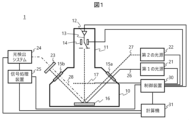
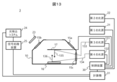
Dans la présente invention, des qualités de film du film semi-conducteur déposé, de film isolant et analogues sont inspectées sans contact. Ce dispositif d'inspection (1) pour inspecter la qualité de film d'un film formé sur un échantillon (16) comporte : une source de particules chargées (12) pour irradier l'échantillon avec un faisceau de particules chargées (13) ; une première source de lumière (21) pour irradier l'échantillon avec une première lumière (26) ; un système de photo-détection pour détecter une lumière de signal (28) générée lorsque l'échantillon est irradié avec la première lumière ; une électrode de commande de charge (17) pour commander un champ électrique sur l'échantillon, ou une seconde source de lumière (22) pour irradier l'échantillon avec une seconde lumière (27) ; un dispositif de commande (30) pour moduler l'état électronique de l'échantillon à l'aide de la source de particules chargées ainsi que de l'électrode de commande de charge ou de la seconde source de lumière ; et un ordinateur (31) pour estimer la qualité de film du film formé sur l'échantillon sur la base d'un signal de détection de lumière de signal qui a été modulé conformément à l'état électronique modulé de l'échantillon, le signal de détection étant délivré depuis le système de photo-détection.
Priority Applications (2)
| Application Number | Priority Date | Filing Date | Title |
|---|---|---|---|
| PCT/JP2022/003391 WO2023145015A1 (fr) | 2022-01-28 | 2022-01-28 | Dispositif d'inspection et procédé d'inspection de qualité de film |
| TW111150350A TW202331771A (zh) | 2022-01-28 | 2022-12-28 | 檢查裝置及膜質檢查方法 |
Applications Claiming Priority (1)
| Application Number | Priority Date | Filing Date | Title |
|---|---|---|---|
| PCT/JP2022/003391 WO2023145015A1 (fr) | 2022-01-28 | 2022-01-28 | Dispositif d'inspection et procédé d'inspection de qualité de film |
Publications (1)
| Publication Number | Publication Date |
|---|---|
| WO2023145015A1 true WO2023145015A1 (fr) | 2023-08-03 |
Family
ID=87470952
Family Applications (1)
| Application Number | Title | Priority Date | Filing Date |
|---|---|---|---|
| PCT/JP2022/003391 WO2023145015A1 (fr) | 2022-01-28 | 2022-01-28 | Dispositif d'inspection et procédé d'inspection de qualité de film |
Country Status (2)
| Country | Link |
|---|---|
| TW (1) | TW202331771A (fr) |
| WO (1) | WO2023145015A1 (fr) |
Citations (7)
| Publication number | Priority date | Publication date | Assignee | Title |
|---|---|---|---|---|
| JPH11118738A (ja) * | 1997-10-14 | 1999-04-30 | Advantest Corp | 微小な測定対象物を高速に分析できる分析装置 |
| JP2000357483A (ja) * | 1999-06-11 | 2000-12-26 | Hitachi Ltd | 荷電粒子線画像に基づく検査または計測方法およびその装置並びに荷電粒子線装置 |
| JP2008027737A (ja) * | 2006-07-21 | 2008-02-07 | Hitachi High-Technologies Corp | パターン検査・計測装置 |
| JP2009043960A (ja) * | 2007-08-09 | 2009-02-26 | Panasonic Corp | 欠陥画像自動収集方法 |
| JP2010097768A (ja) * | 2008-10-15 | 2010-04-30 | Topcon Corp | 複合型観察装置 |
| US20150125065A1 (en) * | 2013-11-04 | 2015-05-07 | Kla-Tencor Corporation | Method and System for Correlating Optical Images with Scanning Electron Microscopy Images |
| JP2017535914A (ja) * | 2014-09-17 | 2017-11-30 | オルボテック エルティーディーOrbotech Ltd. | 検査、テスト、デバッグ、及び表面の改変のための電子ビーム誘導プラズマ(eBIP)の適用 |
-
2022
- 2022-01-28 WO PCT/JP2022/003391 patent/WO2023145015A1/fr active Application Filing
- 2022-12-28 TW TW111150350A patent/TW202331771A/zh unknown
Patent Citations (7)
| Publication number | Priority date | Publication date | Assignee | Title |
|---|---|---|---|---|
| JPH11118738A (ja) * | 1997-10-14 | 1999-04-30 | Advantest Corp | 微小な測定対象物を高速に分析できる分析装置 |
| JP2000357483A (ja) * | 1999-06-11 | 2000-12-26 | Hitachi Ltd | 荷電粒子線画像に基づく検査または計測方法およびその装置並びに荷電粒子線装置 |
| JP2008027737A (ja) * | 2006-07-21 | 2008-02-07 | Hitachi High-Technologies Corp | パターン検査・計測装置 |
| JP2009043960A (ja) * | 2007-08-09 | 2009-02-26 | Panasonic Corp | 欠陥画像自動収集方法 |
| JP2010097768A (ja) * | 2008-10-15 | 2010-04-30 | Topcon Corp | 複合型観察装置 |
| US20150125065A1 (en) * | 2013-11-04 | 2015-05-07 | Kla-Tencor Corporation | Method and System for Correlating Optical Images with Scanning Electron Microscopy Images |
| JP2017535914A (ja) * | 2014-09-17 | 2017-11-30 | オルボテック エルティーディーOrbotech Ltd. | 検査、テスト、デバッグ、及び表面の改変のための電子ビーム誘導プラズマ(eBIP)の適用 |
Also Published As
| Publication number | Publication date |
|---|---|
| TW202331771A (zh) | 2023-08-01 |
Similar Documents
| Publication | Publication Date | Title |
|---|---|---|
| CN112219111B (zh) | 使用于晶片噪声公害识别的扫描式电子显微镜及光学图像相关 | |
| US8586920B2 (en) | Charged particle beam apparatus | |
| JP5009506B2 (ja) | 試料の1つ又は複数の特性を決定するための方法とシステム | |
| EP1907936A2 (fr) | Procede non destructif et systeme pour l'etablissement d'un profil de distribution d'un element dans un film | |
| JP6998469B2 (ja) | 電子線装置 | |
| JP7148467B2 (ja) | 荷電粒子線装置 | |
| TW201407654A (zh) | 歐傑元素識別演算法 | |
| JP2012032239A (ja) | 試料検査装置及び試料検査方法 | |
| TW201834110A (zh) | 整合至一計量及/或檢測工具中之製程模組 | |
| JP2002181725A (ja) | 微小異物解析方法、分析装置、半導体装置の製造方法および液晶表示装置の製造方法 | |
| US20230288355A1 (en) | Electron spectroscopy based techniques for determining various chemical and electrical characteristics of samples | |
| US11107655B2 (en) | Charged particle beam device | |
| US20230035404A1 (en) | Combined ocd and photoreflectance method and system | |
| JP6957633B2 (ja) | 評価用半導体基板およびそれを用いた検査装置の欠陥検出感度評価方法 | |
| WO2023145015A1 (fr) | Dispositif d'inspection et procédé d'inspection de qualité de film | |
| JP2014182984A (ja) | 試料検査装置及び試料の検査方法 | |
| KR20070113655A (ko) | 박막의 두께 측정 방법 및 이를 수행하기 위한 장치 | |
| KR100955434B1 (ko) | 측정된 기초 스펙트럼을 사용하거나 및/또는 획득된스펙트럼에 기초한 박막의 비파괴적 특성화 | |
| US7265343B2 (en) | Apparatus and method for calibration of an optoelectronic sensor and for mensuration of features on a substrate | |
| JP5074262B2 (ja) | 帯電電位測定方法、及び荷電粒子顕微鏡 | |
| JP6677943B2 (ja) | 顕微分光データ測定装置および方法 | |
| WO2024029060A1 (fr) | Dispositif de mesure d'échantillon | |
| JP3361777B2 (ja) | マスク検査方法および検査装置 | |
| JP2957482B2 (ja) | 表面分析法およびその装置 | |
| JP5988958B2 (ja) | 評価方法、評価装置、および半導体装置の製造方法 |
Legal Events
| Date | Code | Title | Description |
|---|---|---|---|
| 121 | Ep: the epo has been informed by wipo that ep was designated in this application |
Ref document number: 22923879 Country of ref document: EP Kind code of ref document: A1 |
|
| WWE | Wipo information: entry into national phase |
Ref document number: 2023576531 Country of ref document: JP |