WO2024029060A1 - Dispositif de mesure d'échantillon - Google Patents
Dispositif de mesure d'échantillon Download PDFInfo
- Publication number
- WO2024029060A1 WO2024029060A1 PCT/JP2022/030067 JP2022030067W WO2024029060A1 WO 2024029060 A1 WO2024029060 A1 WO 2024029060A1 JP 2022030067 W JP2022030067 W JP 2022030067W WO 2024029060 A1 WO2024029060 A1 WO 2024029060A1
- Authority
- WO
- WIPO (PCT)
- Prior art keywords
- sample
- control device
- measuring device
- light
- insulating film
- Prior art date
Links
- 238000001514 detection method Methods 0.000 claims abstract description 58
- 239000002245 particle Substances 0.000 claims abstract description 38
- 239000000463 material Substances 0.000 claims abstract description 25
- 238000000034 method Methods 0.000 claims abstract description 17
- 230000005684 electric field Effects 0.000 claims abstract description 13
- 230000005284 excitation Effects 0.000 claims abstract description 11
- 230000008569 process Effects 0.000 claims abstract description 10
- 230000007547 defect Effects 0.000 claims description 26
- 230000008859 change Effects 0.000 claims description 22
- 230000001678 irradiating effect Effects 0.000 claims description 12
- 238000009826 distribution Methods 0.000 claims description 3
- 238000005259 measurement Methods 0.000 description 107
- 238000006243 chemical reaction Methods 0.000 description 23
- 238000010894 electron beam technology Methods 0.000 description 23
- 239000004065 semiconductor Substances 0.000 description 22
- 238000012545 processing Methods 0.000 description 20
- 238000003384 imaging method Methods 0.000 description 12
- 239000012528 membrane Substances 0.000 description 12
- 230000003287 optical effect Effects 0.000 description 12
- 230000006870 function Effects 0.000 description 11
- 238000003860 storage Methods 0.000 description 11
- 238000004364 calculation method Methods 0.000 description 9
- 101100042258 Neurospora crassa (strain ATCC 24698 / 74-OR23-1A / CBS 708.71 / DSM 1257 / FGSC 987) sem-1 gene Proteins 0.000 description 7
- 230000000694 effects Effects 0.000 description 7
- 230000007423 decrease Effects 0.000 description 6
- XUIMIQQOPSSXEZ-UHFFFAOYSA-N Silicon Chemical compound [Si] XUIMIQQOPSSXEZ-UHFFFAOYSA-N 0.000 description 5
- 229910052710 silicon Inorganic materials 0.000 description 5
- 239000010703 silicon Substances 0.000 description 5
- 230000003068 static effect Effects 0.000 description 5
- 230000004044 response Effects 0.000 description 4
- 230000008030 elimination Effects 0.000 description 3
- 238000003379 elimination reaction Methods 0.000 description 3
- 230000007246 mechanism Effects 0.000 description 3
- 230000010287 polarization Effects 0.000 description 3
- 102100023817 26S proteasome complex subunit SEM1 Human genes 0.000 description 2
- 101000684297 Homo sapiens 26S proteasome complex subunit SEM1 Proteins 0.000 description 2
- 101000873438 Homo sapiens Putative protein SEM1, isoform 2 Proteins 0.000 description 2
- 238000004891 communication Methods 0.000 description 2
- 238000002484 cyclic voltammetry Methods 0.000 description 2
- 230000001419 dependent effect Effects 0.000 description 2
- 230000005611 electricity Effects 0.000 description 2
- 239000012212 insulator Substances 0.000 description 2
- 230000000704 physical effect Effects 0.000 description 2
- 229920006395 saturated elastomer Polymers 0.000 description 2
- 238000001878 scanning electron micrograph Methods 0.000 description 2
- 230000035945 sensitivity Effects 0.000 description 2
- 239000007787 solid Substances 0.000 description 2
- 239000000126 substance Substances 0.000 description 2
- 101100042265 Caenorhabditis elegans sem-2 gene Proteins 0.000 description 1
- 101000650808 Homo sapiens Semaphorin-3G Proteins 0.000 description 1
- 102100027750 Semaphorin-3G Human genes 0.000 description 1
- 230000001133 acceleration Effects 0.000 description 1
- 238000001739 density measurement Methods 0.000 description 1
- 230000004069 differentiation Effects 0.000 description 1
- 238000010884 ion-beam technique Methods 0.000 description 1
- 150000002500 ions Chemical class 0.000 description 1
- 230000006386 memory function Effects 0.000 description 1
- 239000002184 metal Substances 0.000 description 1
- 238000012986 modification Methods 0.000 description 1
- 230000004048 modification Effects 0.000 description 1
- 230000003472 neutralizing effect Effects 0.000 description 1
- 230000001052 transient effect Effects 0.000 description 1
- 229910052724 xenon Inorganic materials 0.000 description 1
- FHNFHKCVQCLJFQ-UHFFFAOYSA-N xenon atom Chemical compound [Xe] FHNFHKCVQCLJFQ-UHFFFAOYSA-N 0.000 description 1
Images


Classifications
-
- G—PHYSICS
- G01—MEASURING; TESTING
- G01N—INVESTIGATING OR ANALYSING MATERIALS BY DETERMINING THEIR CHEMICAL OR PHYSICAL PROPERTIES
- G01N23/00—Investigating or analysing materials by the use of wave or particle radiation, e.g. X-rays or neutrons, not covered by groups G01N3/00 – G01N17/00, G01N21/00 or G01N22/00
- G01N23/22—Investigating or analysing materials by the use of wave or particle radiation, e.g. X-rays or neutrons, not covered by groups G01N3/00 – G01N17/00, G01N21/00 or G01N22/00 by measuring secondary emission from the material
- G01N23/225—Investigating or analysing materials by the use of wave or particle radiation, e.g. X-rays or neutrons, not covered by groups G01N3/00 – G01N17/00, G01N21/00 or G01N22/00 by measuring secondary emission from the material using electron or ion
- G01N23/2251—Investigating or analysing materials by the use of wave or particle radiation, e.g. X-rays or neutrons, not covered by groups G01N3/00 – G01N17/00, G01N21/00 or G01N22/00 by measuring secondary emission from the material using electron or ion using incident electron beams, e.g. scanning electron microscopy [SEM]
Definitions
- the present invention relates to a sample measuring device.
- the quality of the insulating film is important.
- physical properties such as defect (trap) density, defect level, band energy, carrier mobility, carrier lifetime, and material properties of the insulating film or the interface between the insulating film and the semiconductor, including the maximum voltage (withstanding voltage) that can be applied to the insulating film, are discussed. are collectively called membranous.
- One of the insulating films whose film quality is important is the gate oxide film of a transistor. If the gate oxide film has many defects and is of poor quality, charge accumulates in the insulating film over time, changing the performance of the transistor. That is, it reduces the reliability of the device.
- insulating films are also important films used for memory functions by retaining charge.
- the film quality of the insulating film influences the functionality of the memory, such as the volatility of the memory.
- the yield and reliability of semiconductor devices can be improved by timely inspecting and measuring the quality of the insulating film, which is important for devices, during the semiconductor process.
- Patent Document 1 describes an apparatus that uses an electron beam to measure changes in potential on the surface of a semiconductor sample caused by irradiating the sample with light.
- CV measurement which measures the relationship between capacitance and voltage when a target insulating film is sandwiched between electrodes, is known as a method for measuring film quality.
- CV measurement requires forming electrodes on an insulating film, which is time consuming and costly.
- Patent Document 1 evaluates the characteristics of a semiconductor that is not charged by an electron beam.
- the device of Patent Document 1 is insufficient because the insulator is charged by the electron beam and the physical properties to be evaluated are different.
- a sample measuring device includes a light source that irradiates a sample including an insulating film with light, an excitation source that irradiates the sample with a primary beam to emit charged particles, and an electric field or a detector for outputting a detection signal dependent on the energy of the charged particles by applying at least one magnetic field to separate the trajectories depending on the energy of the charged particles;
- the control device includes a control device that processes a detection signal of charged particles, and an input device that inputs information regarding the sample from a user, and the control device processes a detection signal detected by the detector under different irradiation conditions of the light.
- the potential change is converted into a material characteristic value of the insulating film and output.
- a sample measuring device includes: a light source that irradiates a sample including an insulating film with light of a plurality of wavelengths; an excitation source that irradiates the sample with a primary beam to emit charged particles; a detector that outputs a detection signal that depends on the energy of the charged particle by applying at least one of an electric field or a magnetic field to the particle to separate trajectories according to the energy of the charged particle; a control device for processing a detection signal of the charged particles obtained from the detector, the control device processing the detection signal detected by the detector under different irradiation conditions of the light at each of the different wavelengths of the light.
- a comparison signal indicating a comparison result is generated, and information on the film quality of the insulating film based on the comparison signal is output.
- a sample measuring device includes a light source that irradiates a sample including an insulating film with light, an excitation source that irradiates the sample with a primary beam to emit charged particles, and an electric field or a detector for outputting a detection signal dependent on the energy of the charged particles by applying at least one magnetic field to separate the trajectories depending on the energy of the charged particles;
- the control device includes a control device that processes a detection signal of charged particles, and an input device that inputs information about the sample from a user, and the control device changes the light irradiation conditions and performs the detection using the detector under different irradiation conditions.
- a detection signal is acquired, and using information indicating a relationship between the detection signal and the material characteristic value of the insulating film, the material characteristic value is determined and output from the detection signal under the different irradiation conditions.
- desired film quality of a sample can be measured.
- An example of a schematic configuration of a SEM is schematically shown.
- An example of the hardware configuration of the control device is shown.
- a flowchart of an example of SEM control processing by the control device is shown.
- An example of a calibration screen on the settings and measurement screen is shown. It shows a period of irradiation with ultraviolet laser light from a light source, a time change in EF voltage, and a period of imaging (signal electron detection). Indicates detector characteristics.
- the relationship between the EF voltage and the detection signal in different charging states of the sample is schematically shown.
- the relationship between the detected signal amount of signal electrons and the sample potential calculated as described above is shown.
- An example of a setting screen for measuring the film quality of a target sample is shown.
- An example of a sequence of laser light irradiation and imaging under the setting conditions described with reference to FIG. 9 is shown.
- An example of a GUI screen for the measurement stage is shown.
- Another example of a GUI screen for the measurement stage is shown.
- An example of the device configuration of a SEM equipped with a lock-in detection mechanism according to a second embodiment is shown.
- 10 shows a flowchart of an example of SEM control processing by a control device in Example 3.
- An example of a GUI screen at the measurement stage in Example 3 is shown.
- 12 shows a flowchart of an example of SEM control processing performed by a control device according to a fourth embodiment.
- An example of a GUI screen at the measurement stage in Example 4 is shown.
- Example 5 An example of a sequence of laser beam irradiation to a sample and imaging in Example 5 is shown. An example of a sequence of laser beam irradiation to a sample and imaging in Example 5 is shown. An example of a GUI screen at the measurement stage in Example 5 is shown.
- the example apparatus specifically described below measures a sample by using an electron beam as the primary beam and detecting the signal electrons as the signal charged particles.
- the example apparatus specifically described below measures a sample by using an electron beam as the primary beam and detecting the signal electrons as the signal charged particles.
- Features of the present disclosure are also applicable to other devices, such as those that use ion beams or laser light as the primary beam and/or detect ions as signal charged particles.
- FIG. 1 schematically shows an example of a schematic configuration of a scanning electron microscope (SEM) 1.
- the scanning electron microscope device 1 is a sample measuring device according to an embodiment of the present specification that measures material characteristic values of the film quality of a sample, such as the potential and withstand voltage of an insulating film.
- the SEM 1 uses an electron beam to observe and measure a sample.
- the SEM 1 shown in FIG. 1 includes an electron optical system and a control device 112 that controls the electron optical system and measures a sample.
- FIG. 1 shows only some components of the electron optical system.
- Other components not shown in the drawings may be added to the SEM, such as other lenses, aligners, stigmators, deflectors, and separators.
- the optical elements of a SEM (lenses, deflectors, separators, etc.) generate electric fields, magnetic fields, or a combination of magnetic and electric fields and act on the electron beam.
- an objective lens 107 is placed on the trajectory of the primary beam 251 extracted from the excitation source 101 toward the sample 200.
- the excitation source 101 is an electron source (although any other charged particle source, laser, etc. may be used as long as it is an excitation source that emits signal charged particles).
- the primary beam 251 is focused on the sample 200 after passing through the objective lens 107.
- a scanning deflector (not shown) is placed between the excitation source 101 and the objective lens 107, and the direction of the primary beam 251 is controlled so that the primary beam 251 scans an area on the sample 200 two-dimensionally. do.
- the primary beam 251 irradiated onto the sample 200 interacts with substances near the surface, and secondary electrons and other signal electrons are generated depending on the shape and material of the sample.
- the secondary electrons emitted from the sample 200 and detected by the detector 110 are called signal electrons.
- the sample 200 is placed on the stage 108.
- the primary beam 251 irradiated onto the sample 200 interacts with substances near the surface of the sample 200 to generate signal electrons 261 .
- a negative voltage is applied to the stage 108, and an electric field is generated on the sample 200. This electric field causes the signal electrons 261 to reverse the trajectory of the primary beam 251.
- a beam separator not shown, deflects the signal electrons 261 to separate their trajectory from that of the primary beam 251.
- the detector 110 detects the signal electron 261 and converts it into a detection signal.
- the intensity of the detection signal changes depending on the shape and material of the sample 200 at the position irradiated with the primary beam 251.
- An energy filter (EF) 116 is placed in front of the detector 110.
- Energy filter 116 and detector 110 constitute energy detector 106.
- Signal electrons 261 from the sample 200 pass through the energy filter 116 and enter the detector 110.
- Detector 110 detects signal electrons 261 that have passed through energy filter 116.
- Energy filter 116 is connected to EF power supply 111.
- EF power supply 111 provides a voltage set by control device 112 to energy filter 116 .
- the energy filter 116 includes, for example, a metal mesh, and a voltage from the EF power supply 111 is applied thereto. Energy filter 116 either reflects or passes signal electrons 261 depending on the EF voltage being applied. In this way, the energy filter 116 separates the orbits of the signal electrons 261 according to their energy.
- the energy filter 116 uses an electric field to separate the orbits of the signal electrons 261 according to their energies.
- Another example of an energy filter may use a magnetic field to separate the trajectory of the signal electron 261 according to its energy.
- the energy filter may be a spectrometer that does not reflect the signal electrons but deflects them at different angles depending on the energy to separate the signal electrons into orbits.
- the energy detector can output a detection signal that depends on the energy of the signal electrons by applying at least one of an electric field or a magnetic field to the signal electrons to separate their orbits according to the energy of the signal electrons.
- the controller 112 sweeps the EF voltage and determines the EF voltage at which the signal electrons 261 become undetectable or detectable by the detector 110.
- the EF voltage indicating whether or not the signal electron 261 is detected corresponds to the energy of the signal electron 261, and the energy of the signal electron 261 is associated with the potential of the sample 200.
- the sample 200 Since the sample 200 includes an insulator, it is charged by irradiation with the primary beam 251. For example, assume that the sample 200 is positively charged. When the potential of the sample 200 is high, the energy of the detected signal electrons 261 is low. For example, if the energy of the signal electrons 261 is 1 kV when the sample 200 is uncharged, the signal electrons 261 may have a kinetic energy of 990 V when the sample 200 is positively charged.
- Detector 110 measures the signal electronic energy.
- the potential of the sample 200 and the film quality of the sample based on the potential of the sample 200 are measured based on the measurement results of the signal electron energy by the detector 110.
- the film quality to be measured is, for example, defect density [pieces/cm 2 ], carrier mobility [cm 2 /(Vs)], defect level [eV], or band energy [eV] in the insulating film or at the interface. be.
- Defects in the insulating film are not shape defects but material defects such as traps.
- the SEM 1 removes static electricity from the sample 200 by irradiating the sample 200 with light 105 from the light source 103.
- the control device 112 controls the light source 103 and/or the optical path 104, and irradiates the sample 200 with light 105 via the optical path 104.
- the light 105 is, for example, ultraviolet light, and its wavelength may be, for example, 400 nm or less.
- the light source 103 is, for example, an ultraviolet laser.
- the light source 103 may be a white light source made monochromatic using a monochromator. Further, the light source 103 may be composed of a plurality of light sources, and the light source may be selected according to the wavelength setting.
- the control device 112 measures the relationship between the EF voltage and the signal electron energy while the sample 200 is irradiated with the ultraviolet light 105 from the light source 103. As a result, the energy of the signal electrons 261 when the amount of charge on the sample 200 is 0V can be determined. Thereafter, the controller 112 keeps the light 105 OFF in the light source 103 or optical path 104 and measures the relationship between the EF voltage and the signal electron energy. From the two measurement results, the amount of charge [V] of the sample 200 when the sample 200 is irradiated with the primary beam 251 can be determined.
- control device 112 includes a control calculation section 114 and an input/output section 115.
- the control calculation unit 114 controls each component, calculates the signal electron intensity detected by the detector 110, and generates desired information.
- the input/output unit 115 accepts setting operations by the user and presents requested information to the user.
- FIG. 2 shows an example of the hardware configuration of the control device 112.
- Control device 112 can have a computer configuration.
- the control device 112 includes a processor 121 , a memory (main memory) 122 , an auxiliary memory 123 , an output device 124 , an input device 125 , and a communication interface (I/F) 127 .
- the above components are connected to each other by a bus.
- Memory 122, auxiliary storage 123, or a combination thereof is a storage device that stores programs and data used by processor 121.
- the memory 122 is composed of, for example, a semiconductor memory, and is mainly used to hold programs and data that are being executed.
- Processor 121 executes various processes according to programs stored in memory 122.
- Various functional units are realized by the processor 121 operating according to the program.
- the auxiliary storage device 123 is composed of a large-capacity storage device such as a hard disk drive or solid state drive, and is used to retain programs and data for a long period of time.
- the processor 121 can be configured with a single processing unit or multiple processing units, and can include a single or multiple processing units, or multiple processing cores.
- Processor 121 operates on signals based on one or more central processing units, microprocessors, microcomputers, microcontrollers, digital signal processors, state machines, logic circuits, graphics processing units, chip-on-systems, and/or control instructions. It can be implemented as any device.
- Functional units of the control device 112, such as the control calculation unit 114 and the input/output unit 115 can be realized by the processor 121 operating together with other devices according to a program.
- the input/output unit 115 can be implemented by the processor 121 operating together with the output device 124 and the input device 125.
- the programs and data stored in the auxiliary storage device 123 are loaded into the memory 122 at startup or when necessary, and the processor 121 executes the programs, thereby executing various processes of the control device 112. Therefore, the processing executed by the control device 112 below is processing by the processor 121 or the program.
- the input device 125 is a hardware device for a user to input instructions, information, etc. to the control device 112.
- the output device 124 is a hardware device that presents various images for input/output, and is, for example, a display device or a printing device.
- Communication I/F 127 is an interface for connection to a network.
- control device 112 can be implemented in a computer system consisting of one or more computers including one or more processors and one or more storage devices including non-transitory storage media. Multiple computers communicate via a network. For example, some of the multiple functions of the control device 112 may be implemented in one computer, and other parts may be implemented in another computer.
- FIG. 3 shows a flowchart of an example of control processing of the SEM 1 by the control device 112.
- FIG. 3 shows a flow for measuring film quality, for example, material characteristic values such as the amount of charge and withstand voltage of an insulating film.
- the control flow includes three stages: a calibration stage, a setting stage, and a measurement stage.
- the calibration stage consists of steps S11 to S14, the setting stage consists of step S15, and the measurement stage consists of steps S16 to S19.
- the calibration stage performs calibration of the detector 110 and the EF voltage.
- the controller 112 periodically performs a calibration step to enable more accurate measurements of the sample potential of the sample of interest.
- the control device 112 irradiates the sample 200 with light 105 from the light source 103 via the optical path 104.
- the light source 103 is a laser having a wavelength that can remove the charge when the sample 200 is charged, such as an ultraviolet laser.
- the sample 200 is neutralized by the ultraviolet laser beam 105, and the amount of charge becomes 0V.
- step S12 the control device 112 measures the energy characteristics of the signal electrons 261 from the sample, thereby measuring the detector characteristics that indicate the relationship between the detector setting conditions and the signal electron detection signal intensity.
- the control device 112 sweeps (increases or decreases) the EF voltage applied to the energy filter 116 while the sample 200 is irradiated with the ultraviolet laser beam 105.
- the control device 112 irradiates the sample 200 with a primary electron beam at each of different EF voltages, and measures the amount of signal detected by the detector 110 of the signal electrons 261.
- the role of the ultraviolet laser beam 105 irradiation in step S11 is to perform the detector characteristics in step S12 when the sample is not charged, that is, when the amount of charge is 0V. If the same effect can be obtained, the sample 200 may be irradiated with the ultraviolet laser light 105 in step S11 before the EF voltage sweep, always during the EF voltage sweep, or periodically during the EF voltage sweep.
- the primary beam 251 may or may not be scanned two-dimensionally (moved) as long as it is irradiated within the sample 200 area of the same material and thickness.
- the detection intensity of the signal electrons 261 depends on the EF voltage and the configuration of the sample 200, but does not depend on the primary beam irradiation position using the SEM1 optical system.
- step S13 the control device 112 sets the optimal EF voltage for sample measurement based on the measurement results in step S12.
- the control device 112 can determine that the sensitivity of the detection signal of the signal electron 261 to the EF voltage is the optimum EF voltage by changing the EF voltage as described above.
- the EF voltage designated by the user may be set as the optimum EF voltage with reference to the measurement results.
- step S14 the control device 112 generates conversion information for converting the sample potential of the measurement target sample from the detected signal amount of signal electrons from the measurement target sample, and stores it in the auxiliary storage device 123. .
- the sample potential depends on the stage voltage and the amount of charge on the sample 200.
- signal electrons from the sample are measured while applying the optimum voltage determined in step S13 to the energy filter 116.
- the sample potential is calculated from the amount of signal detected by the detector 110 with reference to the conversion information.
- Conversion information may be represented in any format, such as a mathematical formula or a lookup table.
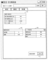
- FIG. 4 shows an example of a calibration screen on the setting and measurement screen.
- the user can input electron beam conditions 301, laser conditions 302, sample conditions 303, and calibration conditions 304 within the calibration screen.
- the user can set the electron beam acceleration voltage, electron beam current, stage voltage, and number of frames as the electron beam conditions 301 for calibration.
- the electron beam is a primary beam 251.
- the stage voltage is a voltage applied to the sample stage 108.
- the number of frames is a value indicating the number of frames used to generate an image of the sample, but if the output of the SEM 1 is not an image, it may be the irradiation time of the primary beam 251, etc.
- the control device 112 two-dimensionally scans the target area of the sample 200 with the primary beam 251 to generate an image.
- the average of four frames is the sample image.
- the detected signal amount may be, for example, the sum or average of the signal amounts of pixels of the image.
- Laser conditions 302 indicate conditions for the light source 103 and optical path 104.
- the wavelength and intensity of laser light can be set as the laser conditions 302.
- Sample condition 303 indicates the coordinates where a sample to be measured for calibration is placed.
- Calibration conditions 304 indicate the range of the EF voltage applied to the energy filter 116 and the set voltage V EF used in measuring the sample potential.
- the set voltage V EF is the final EF voltage obtained as a result of calibration.
- the user can set the sweep range of the EF voltage, and the set voltage VEF is calculated and set by the controller 112.
- the set voltage V EF may be input by the user according to the measurement results in the calibration.
- the user sets the EF voltage range of electron beam conditions 301, laser conditions 302, sample conditions 303, and calibration conditions 304 on the calibration screen.
- the control device 112 executes steps S11 to S14 in the flowchart of FIG.
- the control device 112 displays the detector characteristics 305 obtained through measurement on the calibration screen.
- the horizontal axis shows the EF voltage
- the vertical axis shows the detected signal amount of signal electrons. In a specific EF voltage range, the detected signal amount greatly decreases (increases) as the EF voltage increases (decreases).
- Controller 112 can determine the set voltage V EF based on the graph of detector characteristics 305 . Details of the method for determining the set voltage V EF will be described later.
- the set voltage V EF may be specified by the user. The user refers to the detector characteristics 305 and sets an EF voltage value that he considers appropriate to the cell of the set voltage VEF of the calibration condition 304.
- the set voltage V EF and other conditions 301 to 304 as well as the measurement results 305 of the detector characteristics are saved in the auxiliary storage device 123. At least some information other than the set voltage V EF may be excluded from the stored information.
- FIG. 5 shows a period of irradiation with ultraviolet laser light from the light source 103, a time change in the EF voltage, and a period of imaging (signal electron detection).
- the horizontal axis indicates time. Note that in this specification, both the acquisition of an image when the primary beam is scanned and the acquisition of signal electrons when the primary beam is maintained at one point are referred to as imaging.
- the control device 112 continues to irradiate the sample 200 with ultraviolet laser light during the measurement. That is, the light source 103 is kept ON during the measurement.
- the control device 112 sweeps the EF voltage from a low value to a high value while the sample 200 is irradiated with the laser beam. As shown in FIG. 5, the EF voltage is increased in steps.
- the control device 112 acquires an image of the sample 200. That is, the control device 112 scans a specific range on the sample 200 with the primary beam 251 to obtain an image of the sample 200. As described above, the control device 112 images a predetermined number of frames at each EF voltage value and generates an image based on the average value thereof. The control device 112 may determine the total or average value of the signal amount (brightness) of the pixels of the generated image as the detected signal amount of the signal electrons at the EF voltage.
- the ultraviolet laser light irradiation does not have to be always ON as in this embodiment. If the detection accuracy of signal electrons is degraded by irradiation with ultraviolet laser light, such as when photoelectrons are generated, it is effective to turn off the ultraviolet laser light in synchronization with the ON timing of imaging.
- FIG. 6 shows the detector characteristics.
- the detector characteristics are expressed by the relationship between the EF voltage and the detected signal amount of signal electrons.
- the horizontal axis shows the EF voltage, and the vertical axis shows the detected signal amount of signal electrons.
- the detected signal amount varies greatly within a specific EF voltage range. Specifically, the detected signal amount is approximately constant as the EF voltage increases from the lowest starting voltage to a specific EF voltage, but begins to decrease significantly at the specific EF voltage. The detected signal amount continues to decrease from the specific EF voltage to the specific EF voltage as the EF voltage increases, and thereafter remains approximately constant even if the EF voltage increases.
- the set voltage V EF may be set, for example, to an EF voltage value with the largest absolute value of the rate of change (differentiation) of the detected signal amount.
- FIG. 7 schematically shows the relationship between the EF voltage and the detection signal in different charging states of the sample.
- the horizontal axis shows the EF voltage
- the vertical axis shows the detected signal amount of signal electrons.
- a line 331 indicates the amount of detected signal for the uncharged sample
- a line 332 indicates the amount of detected signal for the charged sample.
- An uncharged sample corresponds to a sample that is measured while being irradiated with laser light for calibration.
- the charged sample corresponds to the sample to be measured.
- its detected signal amount begins to decrease at an EF voltage lower than that of an uncharged sample.
- a point 333A indicates the absolute value of the largest differential.
- Point 333B is a point having the same EF voltage as point 333A in the detected signal amount 332 of the charged sample. The detected signal amount at point 333B is smaller than the detected signal amount at point 333A.
- Point 333C is a point having the same detection signal amount as point 333B in the detection signal amount 331 of the uncharged sample. The EF voltage at point 333C is greater than the EF voltage at point 333B.
- the EF voltage at point 333A is the set voltage V EF at the time of sample measurement.
- the EF voltage difference ⁇ V between point 333C and point 333B indicates the potential difference between the charged sample and the uncharged sample.
- the difference between the set voltage V EF and the EF voltage of the uncharged sample at the detected signal amount of the sample to be measured is the potential difference between the sample to be measured and the uncharged sample.
- the potential difference from the sample potential of the uncharged sample indicates the amount of charge on the measurement sample.
- FIG. 8 shows the relationship between the detected signal amount of signal electrons and the sample potential, which is calculated as described above.
- the sample potential of the sample to be measured is expressed as a function of the amount of detected signal.
- Sample potential [V] f (signal electron detection signal amount)
- the control device 112 constructs conversion information that defines the function shown in FIG. 8 from the relationship 331 between the stage voltage and the EF voltage signal electron detection signal amount of the uncharged sample, which was measured in the calibration stage.
- the conversion information is information for converting the measurement result of the signal electrons of the sample (detected signal amount) into the sample potential, and can be expressed by a look-up table, a mathematical formula, or the like.
- the setting stage consists of step S15.
- the control device 112 sets measurement conditions for the target sample.
- FIG. 9 shows an example of a setting screen for measuring the film quality of the target sample.
- the user can set electron beam conditions 351, measurement conditions 352, and one or more laser conditions 353 corresponding to measurement conditions 352.
- the electron beam conditions 351 specify the primary electron beam, stage voltage, and number of frames, similar to the electron beam conditions 301 in the calibration stage.
- the measurement conditions 352 specify the number of sample measurement conditions and the calculation method for those measurement results.
- the user can specify multiple measurements under different conditions for one sample. In the example shown in FIG. 9, two measurement conditions A and B are specified, and the specified calculation method calculates the difference between the two measurement results.
- the user can specify the conditions for the laser light to be irradiated onto the sample.
- the laser light changes the potential of the sample as described above.
- the light source used for sample measurements may be the same or different from the laser used during the calibration stage.
- the irradiated light does not have to be laser light.
- the irradiated light may be, for example, a white light source such as a xenon lamp made monochromatic using a monochromator.
- FIG. 9 shows the laser conditions of measurement condition B (laser condition B) as an example.
- Laser conditions specify wavelength, intensity and polarization.
- Laser condition A specifies laser light with an intensity of 0, that is, non-irradiation of laser light.
- Laser condition B specifies irradiation with a laser beam having a wavelength of 350 nm, an intensity of 100 mW, and P polarization.
- Another example of two different measurement conditions A and B is that the measurement conditions A and B irradiate laser beams with different wavelengths.
- laser condition A is to irradiate a laser beam of 700 nm
- laser condition B is to irradiate a laser beam of 350 nm.
- the control device 112 calculates the difference between the detection signals at the two measurement stripes.
- the ultraviolet laser light under laser condition B acts on the insulating film using the static elimination effect, but at the same time it also acts on the underlying semiconductor, such as photovoltaic voltage.
- the energy of the signal electrons to be measured is a combination of the effects of the laser on the insulating film and the semiconductor. Since the near-infrared laser light under laser condition A passes through the insulating film, it acts only on the underlying silicon. That is, if the effect on the semiconductor cannot be ignored, the effect on the semiconductor is subtracted by calculating the difference between the measurement results under laser conditions A and B. Therefore, the effect on only the insulating film can be detected and the film quality such as the amount of charge of the insulating film can be appropriately measured.
- the number of measurement laser conditions specified in the measurement conditions 352 is not limited.
- the calculation method specified in the measurement conditions 352 is not limited to subtraction, and any suitable calculation method can be specified depending on the film quality to be calculated.
- FIG. 10 shows an example of a sequence of laser light irradiation and imaging under the setting conditions described with reference to FIG. 9.
- the control device 112 images the sample with the laser turned off (laser condition A) and acquires a signal 1A.
- the control device 112 images the sample in a state where the laser beam is irradiated (laser condition B) and obtains a signal 1B.
- control device 112 images the sample with the laser turned off (laser condition A) and acquires the signal 2A.
- the control device 112 images the sample in a state where the laser beam is irradiated (laser condition B) and obtains a signal 2B.
- control device 112 may determine the average value of the signal 1A and the signal 2A as the image acquired under laser condition A. Further, the control device 112 may determine the average value of the signal 1B and the signal 2B as the image acquired under the laser condition B.
- the measurement stage consists of steps S16 to S19.
- the control device 112 measures the target sample under laser condition A. As described above, under laser condition A, the sample is not irradiated with laser light.
- the control device 112 applies a set voltage V EF to the energy filter 116 without irradiating the laser beam.
- the control device 112 scans the specified region of the sample with the primary beam 252 under the conditions specified by the electron beam conditions 351. As a result, a two-dimensional sample image under laser condition A is obtained.
- step S17 the control device 112 measures the target sample under laser condition B.
- laser condition B specifies irradiation with a laser beam having a wavelength of 350 nm, an intensity of 100 mV, and P polarization.
- Controller 112 provides energy filter 116 with a set voltage V EF .
- the control device 112 scans the designated area of the sample with the primary beam 252 under the conditions specified by the electron beam conditions 351 while irradiating the sample with laser light under the specified conditions. As a result, a two-dimensional sample image under laser condition B is obtained.
- control device 112 may perform measurement (imaging) multiple times under each of the laser conditions A and B, or the number of measurements under each of the laser conditions A and B. may occur only once.
- step S18 the control device 112 determines the sample potential under laser condition A based on the detected signal amount under laser condition A with reference to the conversion information. Furthermore, the control device 112 determines the sample potential under laser condition B based on the detected signal amount under laser condition B and with reference to the conversion information.
- the control device 112 calculates the sample potential change under laser condition A and laser condition B. Using the relationship shown in FIG. 8, a value obtained by subtracting the sample potential under laser condition B from the sample potential under laser condition A is calculated. Note that the control device 112 calculates the difference between the detected signal amount under laser condition A and the detected signal amount under laser condition B, and determines the potential change between the two laser conditions based on the difference and conversion information. You can.
- the difference in detected signal amount and potential change between condition A and condition B are comparison signals representing the comparison results of detected signal amount under these conditions.
- step S19 the control device 112 calculates the film quality according to the calculation method specified by the measurement conditions 352 shown in FIG. 9, and outputs the result.
- the control device 112 subtracts the sample potential under laser condition B from the sample potential under laser condition A according to the measurement conditions specified on the setting screen, and uses the difference as information representing the film quality of the insulating film. Output to the output device 124.
- FIG. 11 shows an example of a GUI screen for the measurement stage.
- the user can specify the coordinates 381 of the measurement target.
- the designated coordinates may be, for example, a reference position of a predetermined scanning area or a position of a point irradiated with the primary beam.
- the user can specify the membrane mass 382 to be displayed.
- the voltage of the sample is specified.
- the amount of charge on the insulating film calculated as described above is displayed.
- the amount of charge is an example of a numerical value representing a change in sample potential.
- the control device 112 may hold reference information for calculating the membrane mass in another designated unit from the calculated sample potential. Thereby, the membrane mass can be displayed in units selected from a plurality of options.
- the measurement GUI screen further shows the measurement results of the sample.
- an SEM image 383 as a comparison target is displayed. This allows the user to visually check the film quality of the target sample in comparison with the structure.
- the measurement area of the sample is composed of, for example, a silicon line 391 and an insulating film 392 formed on silicon in a trench portion between the silicon lines 391.
- the film quality image 384 shows the distribution of the difference between the sample potential under laser condition A and the sample potential under laser condition B in the measurement region.
- the film quality image 384 shows that the amount of charge on the insulating film 392 varies depending on the distance from silicon.
- the amount of charge represents the quality of the insulating film 392.
- FIG. 12 shows another example of the GUI screen for the measurement stage. Compared to the GUI screen example shown in FIG. 11, the displayed measurement results are different.
- the GUI screen in FIG. 12 shows a wafer heat map 387 as a measurement result.
- each measurement result indicates one value.
- the control device 112 can create and display a wafer heat map 387, which is a heat map of the film quality on the wafer.
- the electron beam current is large in the condition setting of S15, the charge on the insulating film is saturated, and the measured charge amount means the withstand voltage of the insulating film. That is, the withstand voltage can also be measured in the same way.
- FIG. 13 shows an example of the device configuration of the SEM 2 equipped with a lock-in detection mechanism. Measurement sensitivity can be improved by using a lock-in detection mechanism.
- SEM2 includes a lock-in amplifier 113 in addition to the components of SEM1 shown in FIG.
- the control device 112 modulates the intensity of the light source 103 at a constant cycle and provides a reference signal with the same cycle to the lock-in amplifier 113.
- the lock-in amplifier 113 enables highly accurate detection by the detector 110 which is modulated in synchronization with this period.
- lock-in detection is particularly effective when the calculation specified by the measurement condition 352 is to calculate the difference between detection signals obtained under two laser conditions.
- Lock-in detection allows the controller 112 to make more accurate and faster measurements than subtraction.
- Example 3 of this specification SEM processing according to Example 3 of this specification will be described below. In the following, differences from Example 1 will be mainly explained.
- the configuration of the SEM of this embodiment may be the same as that of the first embodiment.
- the amount of charge or withstand voltage of the insulating film is presented to the user as a physical quantity (material characteristic value) representing the film quality.
- the control device 112 uses user input to measure and present defect density, which is an example of another physical quantity representing film quality. This embodiment enables accurate defect density measurement.
- FIG. 14 shows a flowchart of an example of control processing of the SEM 1 by the control device 112 in this embodiment. Steps S11 to S18 are similar to steps S11 to S18 in the flowchart of FIG. 3 of the first embodiment.
- step S31 the control device 112 acquires information about the membrane to be measured (membrane information) that has been input in advance by the user.
- the film information is stored in the auxiliary storage device 123, for example.
- the film information can include, for example, film thickness, dielectric constant, and the like.
- step S32 the control device 112 calculates the film quality of the measurement target, in this case the defect density, based on the comparison results of sample potentials (detection signal amount) under different laser conditions and the film information, and Output to the output device 124.
- the control device 112 can calculate the defect density using a preset film quality conversion formula.
- V is the sample potential difference under laser condition A and laser condition B, and is obtained by measurement.
- the control device 112 converts the comparison result of the measured sample potential into a film quality value of defect density using the film information and conversion formula input by the user, and outputs the result.
- the film information includes the dielectric constant ⁇ r and the film thickness d of the insulating film to be measured.
- FIG. 15 shows an example of the GUI screen at the measurement stage.
- the user can input information necessary to measure desired film quality on the GUI screen. Specifically, information about the membrane to be measured and a conversion formula for calculating a desired physical quantity representing the membrane quality can be input. Further, the GUI screen presents the measurement results of the film quality of the sample to the user.
- the user specifies, in addition to measurement coordinates 381, information 401 on the membrane mass to be measured and displayed.
- the membrane mass information 401 specifies a physical quantity to be measured and displayed, membrane information, and a conversion formula for calculating the physical quantity.
- defect density density of material defects
- the film information indicates the film thickness and dielectric constant.
- the user can input a conversion formula into the conversion formula cell. Alternatively, if a simple assumption such as the above conversion formula 2 is sufficient, the control device 112 holds it as default information, and the user can simply select it.
- the measurement GUI screen displays a wafer heat map 402 to the user as a measurement result.
- the wafer heat map 402 is a map showing the relationship between the position on the wafer and the measured defect density.
- the wafer heat map 402 can be created in the same way as the wafer heat map 387 shown in FIG.
- a film quality image indicating defect density may be generated and displayed, such as a film quality image 384 shown in FIG. 11 .
- Example 4 of this specification SEM processing according to Example 4 of this specification will be described below. In the following, differences from Example 1 will be mainly explained.
- the configuration of the SEM of this embodiment may be the same as that of the first embodiment.
- the control device 112 measures and presents defect levels and band energy levels, which are examples of physical quantities representing the film quality of the insulating film.
- defect levels and band energy levels are examples of physical quantities representing the film quality of the insulating film.
- the control device 112 measures the energy level (film quality) from the dependence of the insulating film voltage on the wavelength of light. To measure energy levels, it is necessary to measure the voltage across the insulating film at multiple wavelengths.
- An example of measuring the energy level of an important band in a semiconductor device is measuring the energy level difference between the valence band of a semiconductor and the conduction band of an insulating film. This energy level difference can be determined by measuring the energy required to inject electrons within the semiconductor into the insulating film. Electrons in a semiconductor are excited by absorbing light and gain energy equal to the energy of photons.
- the level energy difference can be calculated by measuring the wavelength of light having a photon energy that can eliminate static electricity from the insulating film.
- the energy level is calculated from the relationship between the insulating film voltage and the wavelength (photon energy) of the irradiated light.
- the control device 112 may control the laser light source 103 so that the number of photons per unit time is the same between wavelengths.
- the number of photons per second is the laser energy divided by the photon energy per second.
- FIG. 16 shows a flowchart of an example of control processing of the SEM 1 by the control device 112 in this embodiment. Steps S11 to S18 are similar to steps S11 to S18 in the flowchart of FIG. 3 of the first embodiment.
- the control device 112 changes either or both of the wavelengths of the laser light irradiated to the sample set under laser condition A and laser condition B (S41), and repeats the loop from steps S16 to S18 with a different laser light wavelength. For example, the wavelength of laser condition B in FIG. 10 is changed. After that, in step S42, the control device 112 determines the energy level from the measurement result of the relationship between the sample potential and the photon energy. The photon energy, which varies greatly in sample potential, determines the energy level difference.
- FIG. 17 shows an example of the GUI screen at the measurement stage.
- the user can input information necessary to measure desired film quality on the measurement GUI screen.
- the energy level is selected as the physical quantity to display the film quality.
- the measurement GUI screen further presents the measurement results of the film quality of the sample to the user.
- the user specifies the membrane mass information 411 to be displayed in addition to the measurement coordinates 381.
- the film mass information 411 specifies an energy level as a physical quantity representing film quality.
- the measurement GUI screen shows a graph 412 showing the relationship between photon energy and sample potential change between conditions A and B as a measurement result.
- the horizontal axis represents photon energy and the vertical axis represents sample voltage.
- the sample potential is the same under laser condition A and laser condition B, so the sample potential change is low and approximately constant.
- static elimination occurs at a specific photon energy, the sample potential measured under laser condition A and laser condition B differs, and the sample potential change starts to increase.
- the sample potential change is approximately constant as the static elimination effect is saturated in the high photon energy region.
- the control device 112 determines the intersection of the tangent to the point where the sample voltage changes the most with respect to a change in photon energy, that is, the point where the absolute value of the differential is the largest, and the approximate straight line in the low photon energy region. It may be determined as an energy level.
- the measurement GUI screen further displays a wafer heat map 413 to the user.
- the wafer heat map 413 is a map showing the relationship between positions on the wafer and measured energy levels.
- the wafer heat map 413 can be created in the same manner as the wafer heat map 387 shown in FIG.
- a film quality image showing the energy level may be generated and displayed, such as a film quality image 384 shown in FIG. 11 .
- the energy level difference between the semiconductor and the insulating film was measured. If the energy level of one side, for example a semiconductor, is known as an absolute value, the energy level of the insulating film can be determined using the measured energy level difference. In addition, if there are traps in the insulating film or its interface, it is possible to excite the electrons held in the traps with light, and similarly to the band energy level difference between the semiconductor and the insulating film, the amount of sample potential change and the photon The trap level can be determined from the energy relationship.
- Example 5 of this specification SEM processing according to Example 5 of this specification will be described below. In the following, differences from Example 1 will be mainly explained.
- the configuration of the SEM of this embodiment may be the same as that of the first embodiment.
- the control device 112 measures and presents carrier life and mobility, which are examples of physical quantities representing film quality. This embodiment enables accurate measurement of carrier lifetime and mobility.
- the control device 112 measures carrier life and mobility from the time difference between pulsed light irradiation and pulsed electron beam (primary beam) irradiation. Carrier lifetime and mobility appear in the transient response of measurements.
- FIG. 18 shows an example of a sequence of laser beam irradiation and imaging (primary beam irradiation) on a sample.
- the control device 112 images the sample with the laser turned off (laser condition A) and acquires the signal 1A.
- the control device 112 images the sample after a predetermined waiting time (DELAY) and acquires the signal 1B.
- DELAY waiting time
- signal 1A and signal 1B are acquired.
- Signals 2A, 2B are then obtained by measurements at different latencies. Thereafter, measurements are repeated with different waiting times.
- the control device 112 does not acquire the signal 1B by simultaneous irradiation with a laser beam and an electron beam (primary beam), but instead sets a time difference (DELAY) between the laser beam irradiation and the electron beam irradiation. establish.
- the control device 112 can measure the response of the insulating film and its interface to light by controlling the length of the waiting time and measuring the dependency of the measured potential change on the waiting time.
- the control device 112 uses a conversion formula to convert the response characteristics into carrier lifetime and mobility.
- This conversion formula takes waiting time as a factor. For example, carrier life and mobility can be calculated from the waiting time at which the sample potential changes significantly using a conversion formula.
- FIG. 19 shows an example of a sequence of laser beam irradiation to a sample and imaging (primary beam irradiation).
- the control device 112 images the sample and acquires the signal 1A without irradiating the sample with laser light (laser 1 condition A and laser 2 condition A).
- the control device 112 controls the sample while irradiating laser beam 2 (laser 2 condition B). Imaging is performed and signal 1B is acquired. In one measurement, signal 1A and signal 1B are acquired. Signals 2A, 2B are then obtained by measurements at different latencies. Thereafter, measurements are repeated with different waiting times.
- the control device 112 can calculate and output the response characteristic of the phenomenon from the relationship between the sample potential change and the waiting time.
- the waiting time (time difference) can be input as a set value by the user on the measurement GUI screen.
- the control device 112 can display, as a measurement result, a graph in which the horizontal axis indicates the waiting time and the vertical axis indicates the sample potential change.
- a heat map or film quality image indicating carrier life and mobility may be generated and displayed.
- FIG. 20 shows an example of the GUI screen at the measurement stage.
- the user can input information necessary to measure desired film quality on the measurement GUI screen.
- carrier life is selected as the physical quantity to display film quality.
- the measurement GUI screen further presents the measurement results of the film quality of the sample to the user.
- the user specifies the membrane mass information 411 to be displayed in addition to the measurement coordinates 381.
- the film mass information 411 specifies carrier life as a physical quantity representing film quality.
- the measurement GUI screen shows a graph 432 showing the relationship between waiting time and sample potential change between conditions A and B as a measurement result.
- the horizontal axis shows waiting time and the vertical axis shows sample voltage.
- the control device 112 determines the intersection of the tangent to the point where the sample voltage changes the most with respect to a change in the waiting time, that is, the point where the absolute value of the differential is the largest, and the approximate straight line in the region of the large waiting time. may be determined to have a career life of .
- the measurement GUI screen further displays a wafer heat map 433 to the user.
- the wafer heat map 433 is a map showing the relationship between the position on the wafer and the measured carrier life.
- the wafer heat map 413 can be created in the same way as the wafer heat map 387 shown in FIG.
- a film quality image indicating the carrier life may be generated and displayed, such as a film quality image 384 shown in FIG. 11 .
- the present invention is not limited to the above-described embodiments, and includes various modifications.
- the embodiments described above are described in detail to explain the present invention in an easy-to-understand manner, and the present invention is not necessarily limited to having all the configurations described.
- it is possible to replace a part of the configuration of one embodiment with the configuration of another embodiment and it is also possible to add the configuration of another embodiment to the configuration of one embodiment.
- each of the configurations, functions, processing units, etc. described above may be partially or entirely realized in hardware by, for example, designing an integrated circuit.
- each of the above-mentioned configurations, functions, etc. may be realized by software by a processor interpreting and executing a program for realizing each function.
- Information such as programs, tables, files, etc. that implement each function can be stored in a memory, a recording device such as a hard disk, an SSD (Solid State Drive), or a recording medium such as an IC card or an SD card.
- control lines and information lines are shown that are considered necessary for explanation, and not all control lines and information lines are necessarily shown in the product. In reality, almost all configurations may be considered interconnected.
Landscapes
- Physics & Mathematics (AREA)
- Health & Medical Sciences (AREA)
- Life Sciences & Earth Sciences (AREA)
- Chemical & Material Sciences (AREA)
- Analytical Chemistry (AREA)
- Biochemistry (AREA)
- General Health & Medical Sciences (AREA)
- General Physics & Mathematics (AREA)
- Immunology (AREA)
- Pathology (AREA)
- Analysing Materials By The Use Of Radiation (AREA)
- Testing Or Measuring Of Semiconductors Or The Like (AREA)
Abstract
L'invention concerne un dispositif de mesure d'échantillon qui comprend : une source de lumière qui irradie un échantillon comprenant un film isolant avec de la lumière ; une source d'excitation qui irradie l'échantillon avec un faisceau primaire pour émettre des particules chargées ; un détecteur qui applique un champ électrique et/ou un champ magnétique aux particules chargées pour séparer les trajectoires en fonction de l'énergie des particules chargées, et délivre un signal de détection qui dépend de l'énergie des particules chargées ; et un dispositif de commande qui traite le signal de détection des particules chargées obtenues à partir du détecteur. Le dispositif de commande change une condition d'irradiation de lumière, acquiert un signal de détection par le détecteur dans une condition d'irradiation différente, et détermine et fournit des valeurs caractéristiques de matériau à partir du signal de détection dans la condition d'irradiation différente en utilisant des informations indiquant la relation entre le signal de détection et les valeurs caractéristiques de matériau du film isolant.
Priority Applications (2)
| Application Number | Priority Date | Filing Date | Title |
|---|---|---|---|
| PCT/JP2022/030067 WO2024029060A1 (fr) | 2022-08-05 | 2022-08-05 | Dispositif de mesure d'échantillon |
| TW112121830A TW202407342A (zh) | 2022-08-05 | 2023-06-12 | 試料測定裝置 |
Applications Claiming Priority (1)
| Application Number | Priority Date | Filing Date | Title |
|---|---|---|---|
| PCT/JP2022/030067 WO2024029060A1 (fr) | 2022-08-05 | 2022-08-05 | Dispositif de mesure d'échantillon |
Publications (1)
| Publication Number | Publication Date |
|---|---|
| WO2024029060A1 true WO2024029060A1 (fr) | 2024-02-08 |
Family
ID=89848742
Family Applications (1)
| Application Number | Title | Priority Date | Filing Date |
|---|---|---|---|
| PCT/JP2022/030067 WO2024029060A1 (fr) | 2022-08-05 | 2022-08-05 | Dispositif de mesure d'échantillon |
Country Status (2)
| Country | Link |
|---|---|
| TW (1) | TW202407342A (fr) |
| WO (1) | WO2024029060A1 (fr) |
Citations (7)
| Publication number | Priority date | Publication date | Assignee | Title |
|---|---|---|---|---|
| JPH09162253A (ja) * | 1995-12-08 | 1997-06-20 | Hitachi Ltd | 半導体評価装置 |
| JP2001093892A (ja) * | 1999-08-17 | 2001-04-06 | Samsung Electronics Co Ltd | 半導体装置の製造において使われるプラズマによって誘起される電荷帯電程度を判別する方法およびこれに用いられる判別装置 |
| WO2007129596A1 (fr) * | 2006-05-02 | 2007-11-15 | The University Of Tokyo | Procédé de mesure de niveau d'énergie et procédé d'analyse de niveau d'énergie |
| JP2010216931A (ja) * | 2009-03-16 | 2010-09-30 | Ricoh Co Ltd | 静電潜像の評価方法、静電潜像の評価装置および画像形成装置 |
| JP2014182984A (ja) * | 2013-03-21 | 2014-09-29 | Ebara Corp | 試料検査装置及び試料の検査方法 |
| WO2017158742A1 (fr) * | 2016-03-16 | 2017-09-21 | 株式会社 日立ハイテクノロジーズ | Dispositif d'inspection de défauts |
| JP2021039844A (ja) * | 2019-08-30 | 2021-03-11 | 株式会社日立ハイテク | 荷電粒子線装置 |
-
2022
- 2022-08-05 WO PCT/JP2022/030067 patent/WO2024029060A1/fr unknown
-
2023
- 2023-06-12 TW TW112121830A patent/TW202407342A/zh unknown
Patent Citations (7)
| Publication number | Priority date | Publication date | Assignee | Title |
|---|---|---|---|---|
| JPH09162253A (ja) * | 1995-12-08 | 1997-06-20 | Hitachi Ltd | 半導体評価装置 |
| JP2001093892A (ja) * | 1999-08-17 | 2001-04-06 | Samsung Electronics Co Ltd | 半導体装置の製造において使われるプラズマによって誘起される電荷帯電程度を判別する方法およびこれに用いられる判別装置 |
| WO2007129596A1 (fr) * | 2006-05-02 | 2007-11-15 | The University Of Tokyo | Procédé de mesure de niveau d'énergie et procédé d'analyse de niveau d'énergie |
| JP2010216931A (ja) * | 2009-03-16 | 2010-09-30 | Ricoh Co Ltd | 静電潜像の評価方法、静電潜像の評価装置および画像形成装置 |
| JP2014182984A (ja) * | 2013-03-21 | 2014-09-29 | Ebara Corp | 試料検査装置及び試料の検査方法 |
| WO2017158742A1 (fr) * | 2016-03-16 | 2017-09-21 | 株式会社 日立ハイテクノロジーズ | Dispositif d'inspection de défauts |
| JP2021039844A (ja) * | 2019-08-30 | 2021-03-11 | 株式会社日立ハイテク | 荷電粒子線装置 |
Also Published As
| Publication number | Publication date |
|---|---|
| TW202407342A (zh) | 2024-02-16 |
Similar Documents
| Publication | Publication Date | Title |
|---|---|---|
| US10840060B2 (en) | Scanning electron microscope and sample observation method | |
| EP2530699B1 (fr) | Microscope à faisceau de particules chargées et son emploi pour une technique de mesure | |
| US7652248B2 (en) | Inspection apparatus and inspection method | |
| JP4519567B2 (ja) | 走査型電子顕微鏡およびこれを用いた試料観察方法 | |
| US9324540B2 (en) | Charged particle beam device | |
| KR102443807B1 (ko) | 하전 입자선 장치 | |
| US8923614B2 (en) | Image processing apparatus, image processing method | |
| JP2006019301A (ja) | 電子ビームの調整方法,荷電粒子光学系制御装置、及び走査電子顕微鏡 | |
| JP6782795B2 (ja) | 走査電子顕微鏡および走査電子顕微鏡による試料観察方法 | |
| US8507857B2 (en) | Charged particle beam inspection apparatus and inspection method using charged particle beam | |
| US7714288B2 (en) | Charged particle beam apparatus | |
| WO2024029060A1 (fr) | Dispositif de mesure d'échantillon | |
| JP4095510B2 (ja) | 表面電位測定方法及び試料観察方法 | |
| US7205539B1 (en) | Sample charging control in charged-particle systems | |
| WO2022091180A1 (fr) | Dispositif à faisceau de particules chargées | |
| JP2005026192A (ja) | 荷電粒子ビーム装置 | |
| KR102625536B1 (ko) | 하전 입자빔 시스템, 및 하전 입자선 장치에 있어서의 관찰 조건을 결정하는 방법 | |
| JP6230831B2 (ja) | 荷電粒子線装置および画像取得方法 | |
| WO2022208572A1 (fr) | Système d'inspection | |
| US20240055221A1 (en) | Dual-use read-out circuitry in charged particle detection system | |
| WO2023145015A1 (fr) | Dispositif d'inspection et procédé d'inspection de qualité de film | |
| JP4954470B2 (ja) | 電流測定装置 |
Legal Events
| Date | Code | Title | Description |
|---|---|---|---|
| 121 | Ep: the epo has been informed by wipo that ep was designated in this application |
Ref document number: 22954048 Country of ref document: EP Kind code of ref document: A1 |