WO2024029060A1 - Sample measuring device - Google Patents
Sample measuring device Download PDFInfo
- Publication number
- WO2024029060A1 WO2024029060A1 PCT/JP2022/030067 JP2022030067W WO2024029060A1 WO 2024029060 A1 WO2024029060 A1 WO 2024029060A1 JP 2022030067 W JP2022030067 W JP 2022030067W WO 2024029060 A1 WO2024029060 A1 WO 2024029060A1
- Authority
- WO
- WIPO (PCT)
- Prior art keywords
- sample
- control device
- measuring device
- light
- insulating film
- Prior art date
Links
- 238000001514 detection method Methods 0.000 claims abstract description 58
- 239000002245 particle Substances 0.000 claims abstract description 38
- 239000000463 material Substances 0.000 claims abstract description 25
- 238000000034 method Methods 0.000 claims abstract description 17
- 230000005684 electric field Effects 0.000 claims abstract description 13
- 230000005284 excitation Effects 0.000 claims abstract description 11
- 230000008569 process Effects 0.000 claims abstract description 10
- 230000007547 defect Effects 0.000 claims description 26
- 230000008859 change Effects 0.000 claims description 22
- 230000001678 irradiating effect Effects 0.000 claims description 12
- 238000009826 distribution Methods 0.000 claims description 3
- 238000005259 measurement Methods 0.000 description 107
- 238000006243 chemical reaction Methods 0.000 description 23
- 238000010894 electron beam technology Methods 0.000 description 23
- 239000004065 semiconductor Substances 0.000 description 22
- 238000012545 processing Methods 0.000 description 20
- 238000003384 imaging method Methods 0.000 description 12
- 239000012528 membrane Substances 0.000 description 12
- 230000003287 optical effect Effects 0.000 description 12
- 230000006870 function Effects 0.000 description 11
- 238000003860 storage Methods 0.000 description 11
- 238000004364 calculation method Methods 0.000 description 9
- 101100042258 Neurospora crassa (strain ATCC 24698 / 74-OR23-1A / CBS 708.71 / DSM 1257 / FGSC 987) sem-1 gene Proteins 0.000 description 7
- 230000000694 effects Effects 0.000 description 7
- 230000007423 decrease Effects 0.000 description 6
- XUIMIQQOPSSXEZ-UHFFFAOYSA-N Silicon Chemical compound [Si] XUIMIQQOPSSXEZ-UHFFFAOYSA-N 0.000 description 5
- 229910052710 silicon Inorganic materials 0.000 description 5
- 239000010703 silicon Substances 0.000 description 5
- 230000003068 static effect Effects 0.000 description 5
- 230000004044 response Effects 0.000 description 4
- 230000008030 elimination Effects 0.000 description 3
- 238000003379 elimination reaction Methods 0.000 description 3
- 230000007246 mechanism Effects 0.000 description 3
- 230000010287 polarization Effects 0.000 description 3
- 102100023817 26S proteasome complex subunit SEM1 Human genes 0.000 description 2
- 101000684297 Homo sapiens 26S proteasome complex subunit SEM1 Proteins 0.000 description 2
- 101000873438 Homo sapiens Putative protein SEM1, isoform 2 Proteins 0.000 description 2
- 238000004891 communication Methods 0.000 description 2
- 238000002484 cyclic voltammetry Methods 0.000 description 2
- 230000001419 dependent effect Effects 0.000 description 2
- 230000005611 electricity Effects 0.000 description 2
- 239000012212 insulator Substances 0.000 description 2
- 230000000704 physical effect Effects 0.000 description 2
- 229920006395 saturated elastomer Polymers 0.000 description 2
- 238000001878 scanning electron micrograph Methods 0.000 description 2
- 230000035945 sensitivity Effects 0.000 description 2
- 239000007787 solid Substances 0.000 description 2
- 239000000126 substance Substances 0.000 description 2
- 101100042265 Caenorhabditis elegans sem-2 gene Proteins 0.000 description 1
- 101000650808 Homo sapiens Semaphorin-3G Proteins 0.000 description 1
- 102100027750 Semaphorin-3G Human genes 0.000 description 1
- 230000001133 acceleration Effects 0.000 description 1
- 238000001739 density measurement Methods 0.000 description 1
- 230000004069 differentiation Effects 0.000 description 1
- 238000010884 ion-beam technique Methods 0.000 description 1
- 150000002500 ions Chemical class 0.000 description 1
- 230000006386 memory function Effects 0.000 description 1
- 239000002184 metal Substances 0.000 description 1
- 238000012986 modification Methods 0.000 description 1
- 230000004048 modification Effects 0.000 description 1
- 230000003472 neutralizing effect Effects 0.000 description 1
- 230000001052 transient effect Effects 0.000 description 1
- 229910052724 xenon Inorganic materials 0.000 description 1
- FHNFHKCVQCLJFQ-UHFFFAOYSA-N xenon atom Chemical compound [Xe] FHNFHKCVQCLJFQ-UHFFFAOYSA-N 0.000 description 1
Images


Classifications
-
- G—PHYSICS
- G01—MEASURING; TESTING
- G01N—INVESTIGATING OR ANALYSING MATERIALS BY DETERMINING THEIR CHEMICAL OR PHYSICAL PROPERTIES
- G01N23/00—Investigating or analysing materials by the use of wave or particle radiation, e.g. X-rays or neutrons, not covered by groups G01N3/00 – G01N17/00, G01N21/00 or G01N22/00
- G01N23/22—Investigating or analysing materials by the use of wave or particle radiation, e.g. X-rays or neutrons, not covered by groups G01N3/00 – G01N17/00, G01N21/00 or G01N22/00 by measuring secondary emission from the material
- G01N23/225—Investigating or analysing materials by the use of wave or particle radiation, e.g. X-rays or neutrons, not covered by groups G01N3/00 – G01N17/00, G01N21/00 or G01N22/00 by measuring secondary emission from the material using electron or ion
- G01N23/2251—Investigating or analysing materials by the use of wave or particle radiation, e.g. X-rays or neutrons, not covered by groups G01N3/00 – G01N17/00, G01N21/00 or G01N22/00 by measuring secondary emission from the material using electron or ion using incident electron beams, e.g. scanning electron microscopy [SEM]
Definitions
- the present invention relates to a sample measuring device.
- the quality of the insulating film is important.
- physical properties such as defect (trap) density, defect level, band energy, carrier mobility, carrier lifetime, and material properties of the insulating film or the interface between the insulating film and the semiconductor, including the maximum voltage (withstanding voltage) that can be applied to the insulating film, are discussed. are collectively called membranous.
- One of the insulating films whose film quality is important is the gate oxide film of a transistor. If the gate oxide film has many defects and is of poor quality, charge accumulates in the insulating film over time, changing the performance of the transistor. That is, it reduces the reliability of the device.
- insulating films are also important films used for memory functions by retaining charge.
- the film quality of the insulating film influences the functionality of the memory, such as the volatility of the memory.
- the yield and reliability of semiconductor devices can be improved by timely inspecting and measuring the quality of the insulating film, which is important for devices, during the semiconductor process.
- Patent Document 1 describes an apparatus that uses an electron beam to measure changes in potential on the surface of a semiconductor sample caused by irradiating the sample with light.
- CV measurement which measures the relationship between capacitance and voltage when a target insulating film is sandwiched between electrodes, is known as a method for measuring film quality.
- CV measurement requires forming electrodes on an insulating film, which is time consuming and costly.
- Patent Document 1 evaluates the characteristics of a semiconductor that is not charged by an electron beam.
- the device of Patent Document 1 is insufficient because the insulator is charged by the electron beam and the physical properties to be evaluated are different.
- a sample measuring device includes a light source that irradiates a sample including an insulating film with light, an excitation source that irradiates the sample with a primary beam to emit charged particles, and an electric field or a detector for outputting a detection signal dependent on the energy of the charged particles by applying at least one magnetic field to separate the trajectories depending on the energy of the charged particles;
- the control device includes a control device that processes a detection signal of charged particles, and an input device that inputs information regarding the sample from a user, and the control device processes a detection signal detected by the detector under different irradiation conditions of the light.
- the potential change is converted into a material characteristic value of the insulating film and output.
- a sample measuring device includes: a light source that irradiates a sample including an insulating film with light of a plurality of wavelengths; an excitation source that irradiates the sample with a primary beam to emit charged particles; a detector that outputs a detection signal that depends on the energy of the charged particle by applying at least one of an electric field or a magnetic field to the particle to separate trajectories according to the energy of the charged particle; a control device for processing a detection signal of the charged particles obtained from the detector, the control device processing the detection signal detected by the detector under different irradiation conditions of the light at each of the different wavelengths of the light.
- a comparison signal indicating a comparison result is generated, and information on the film quality of the insulating film based on the comparison signal is output.
- a sample measuring device includes a light source that irradiates a sample including an insulating film with light, an excitation source that irradiates the sample with a primary beam to emit charged particles, and an electric field or a detector for outputting a detection signal dependent on the energy of the charged particles by applying at least one magnetic field to separate the trajectories depending on the energy of the charged particles;
- the control device includes a control device that processes a detection signal of charged particles, and an input device that inputs information about the sample from a user, and the control device changes the light irradiation conditions and performs the detection using the detector under different irradiation conditions.
- a detection signal is acquired, and using information indicating a relationship between the detection signal and the material characteristic value of the insulating film, the material characteristic value is determined and output from the detection signal under the different irradiation conditions.
- desired film quality of a sample can be measured.
- An example of a schematic configuration of a SEM is schematically shown.
- An example of the hardware configuration of the control device is shown.
- a flowchart of an example of SEM control processing by the control device is shown.
- An example of a calibration screen on the settings and measurement screen is shown. It shows a period of irradiation with ultraviolet laser light from a light source, a time change in EF voltage, and a period of imaging (signal electron detection). Indicates detector characteristics.
- the relationship between the EF voltage and the detection signal in different charging states of the sample is schematically shown.
- the relationship between the detected signal amount of signal electrons and the sample potential calculated as described above is shown.
- An example of a setting screen for measuring the film quality of a target sample is shown.
- An example of a sequence of laser light irradiation and imaging under the setting conditions described with reference to FIG. 9 is shown.
- An example of a GUI screen for the measurement stage is shown.
- Another example of a GUI screen for the measurement stage is shown.
- An example of the device configuration of a SEM equipped with a lock-in detection mechanism according to a second embodiment is shown.
- 10 shows a flowchart of an example of SEM control processing by a control device in Example 3.
- An example of a GUI screen at the measurement stage in Example 3 is shown.
- 12 shows a flowchart of an example of SEM control processing performed by a control device according to a fourth embodiment.
- An example of a GUI screen at the measurement stage in Example 4 is shown.
- Example 5 An example of a sequence of laser beam irradiation to a sample and imaging in Example 5 is shown. An example of a sequence of laser beam irradiation to a sample and imaging in Example 5 is shown. An example of a GUI screen at the measurement stage in Example 5 is shown.
- the example apparatus specifically described below measures a sample by using an electron beam as the primary beam and detecting the signal electrons as the signal charged particles.
- the example apparatus specifically described below measures a sample by using an electron beam as the primary beam and detecting the signal electrons as the signal charged particles.
- Features of the present disclosure are also applicable to other devices, such as those that use ion beams or laser light as the primary beam and/or detect ions as signal charged particles.
- FIG. 1 schematically shows an example of a schematic configuration of a scanning electron microscope (SEM) 1.
- the scanning electron microscope device 1 is a sample measuring device according to an embodiment of the present specification that measures material characteristic values of the film quality of a sample, such as the potential and withstand voltage of an insulating film.
- the SEM 1 uses an electron beam to observe and measure a sample.
- the SEM 1 shown in FIG. 1 includes an electron optical system and a control device 112 that controls the electron optical system and measures a sample.
- FIG. 1 shows only some components of the electron optical system.
- Other components not shown in the drawings may be added to the SEM, such as other lenses, aligners, stigmators, deflectors, and separators.
- the optical elements of a SEM (lenses, deflectors, separators, etc.) generate electric fields, magnetic fields, or a combination of magnetic and electric fields and act on the electron beam.
- an objective lens 107 is placed on the trajectory of the primary beam 251 extracted from the excitation source 101 toward the sample 200.
- the excitation source 101 is an electron source (although any other charged particle source, laser, etc. may be used as long as it is an excitation source that emits signal charged particles).
- the primary beam 251 is focused on the sample 200 after passing through the objective lens 107.
- a scanning deflector (not shown) is placed between the excitation source 101 and the objective lens 107, and the direction of the primary beam 251 is controlled so that the primary beam 251 scans an area on the sample 200 two-dimensionally. do.
- the primary beam 251 irradiated onto the sample 200 interacts with substances near the surface, and secondary electrons and other signal electrons are generated depending on the shape and material of the sample.
- the secondary electrons emitted from the sample 200 and detected by the detector 110 are called signal electrons.
- the sample 200 is placed on the stage 108.
- the primary beam 251 irradiated onto the sample 200 interacts with substances near the surface of the sample 200 to generate signal electrons 261 .
- a negative voltage is applied to the stage 108, and an electric field is generated on the sample 200. This electric field causes the signal electrons 261 to reverse the trajectory of the primary beam 251.
- a beam separator not shown, deflects the signal electrons 261 to separate their trajectory from that of the primary beam 251.
- the detector 110 detects the signal electron 261 and converts it into a detection signal.
- the intensity of the detection signal changes depending on the shape and material of the sample 200 at the position irradiated with the primary beam 251.
- An energy filter (EF) 116 is placed in front of the detector 110.
- Energy filter 116 and detector 110 constitute energy detector 106.
- Signal electrons 261 from the sample 200 pass through the energy filter 116 and enter the detector 110.
- Detector 110 detects signal electrons 261 that have passed through energy filter 116.
- Energy filter 116 is connected to EF power supply 111.
- EF power supply 111 provides a voltage set by control device 112 to energy filter 116 .
- the energy filter 116 includes, for example, a metal mesh, and a voltage from the EF power supply 111 is applied thereto. Energy filter 116 either reflects or passes signal electrons 261 depending on the EF voltage being applied. In this way, the energy filter 116 separates the orbits of the signal electrons 261 according to their energy.
- the energy filter 116 uses an electric field to separate the orbits of the signal electrons 261 according to their energies.
- Another example of an energy filter may use a magnetic field to separate the trajectory of the signal electron 261 according to its energy.
- the energy filter may be a spectrometer that does not reflect the signal electrons but deflects them at different angles depending on the energy to separate the signal electrons into orbits.
- the energy detector can output a detection signal that depends on the energy of the signal electrons by applying at least one of an electric field or a magnetic field to the signal electrons to separate their orbits according to the energy of the signal electrons.
- the controller 112 sweeps the EF voltage and determines the EF voltage at which the signal electrons 261 become undetectable or detectable by the detector 110.
- the EF voltage indicating whether or not the signal electron 261 is detected corresponds to the energy of the signal electron 261, and the energy of the signal electron 261 is associated with the potential of the sample 200.
- the sample 200 Since the sample 200 includes an insulator, it is charged by irradiation with the primary beam 251. For example, assume that the sample 200 is positively charged. When the potential of the sample 200 is high, the energy of the detected signal electrons 261 is low. For example, if the energy of the signal electrons 261 is 1 kV when the sample 200 is uncharged, the signal electrons 261 may have a kinetic energy of 990 V when the sample 200 is positively charged.
- Detector 110 measures the signal electronic energy.
- the potential of the sample 200 and the film quality of the sample based on the potential of the sample 200 are measured based on the measurement results of the signal electron energy by the detector 110.
- the film quality to be measured is, for example, defect density [pieces/cm 2 ], carrier mobility [cm 2 /(Vs)], defect level [eV], or band energy [eV] in the insulating film or at the interface. be.
- Defects in the insulating film are not shape defects but material defects such as traps.
- the SEM 1 removes static electricity from the sample 200 by irradiating the sample 200 with light 105 from the light source 103.
- the control device 112 controls the light source 103 and/or the optical path 104, and irradiates the sample 200 with light 105 via the optical path 104.
- the light 105 is, for example, ultraviolet light, and its wavelength may be, for example, 400 nm or less.
- the light source 103 is, for example, an ultraviolet laser.
- the light source 103 may be a white light source made monochromatic using a monochromator. Further, the light source 103 may be composed of a plurality of light sources, and the light source may be selected according to the wavelength setting.
- the control device 112 measures the relationship between the EF voltage and the signal electron energy while the sample 200 is irradiated with the ultraviolet light 105 from the light source 103. As a result, the energy of the signal electrons 261 when the amount of charge on the sample 200 is 0V can be determined. Thereafter, the controller 112 keeps the light 105 OFF in the light source 103 or optical path 104 and measures the relationship between the EF voltage and the signal electron energy. From the two measurement results, the amount of charge [V] of the sample 200 when the sample 200 is irradiated with the primary beam 251 can be determined.
- control device 112 includes a control calculation section 114 and an input/output section 115.
- the control calculation unit 114 controls each component, calculates the signal electron intensity detected by the detector 110, and generates desired information.
- the input/output unit 115 accepts setting operations by the user and presents requested information to the user.
- FIG. 2 shows an example of the hardware configuration of the control device 112.
- Control device 112 can have a computer configuration.
- the control device 112 includes a processor 121 , a memory (main memory) 122 , an auxiliary memory 123 , an output device 124 , an input device 125 , and a communication interface (I/F) 127 .
- the above components are connected to each other by a bus.
- Memory 122, auxiliary storage 123, or a combination thereof is a storage device that stores programs and data used by processor 121.
- the memory 122 is composed of, for example, a semiconductor memory, and is mainly used to hold programs and data that are being executed.
- Processor 121 executes various processes according to programs stored in memory 122.
- Various functional units are realized by the processor 121 operating according to the program.
- the auxiliary storage device 123 is composed of a large-capacity storage device such as a hard disk drive or solid state drive, and is used to retain programs and data for a long period of time.
- the processor 121 can be configured with a single processing unit or multiple processing units, and can include a single or multiple processing units, or multiple processing cores.
- Processor 121 operates on signals based on one or more central processing units, microprocessors, microcomputers, microcontrollers, digital signal processors, state machines, logic circuits, graphics processing units, chip-on-systems, and/or control instructions. It can be implemented as any device.
- Functional units of the control device 112, such as the control calculation unit 114 and the input/output unit 115 can be realized by the processor 121 operating together with other devices according to a program.
- the input/output unit 115 can be implemented by the processor 121 operating together with the output device 124 and the input device 125.
- the programs and data stored in the auxiliary storage device 123 are loaded into the memory 122 at startup or when necessary, and the processor 121 executes the programs, thereby executing various processes of the control device 112. Therefore, the processing executed by the control device 112 below is processing by the processor 121 or the program.
- the input device 125 is a hardware device for a user to input instructions, information, etc. to the control device 112.
- the output device 124 is a hardware device that presents various images for input/output, and is, for example, a display device or a printing device.
- Communication I/F 127 is an interface for connection to a network.
- control device 112 can be implemented in a computer system consisting of one or more computers including one or more processors and one or more storage devices including non-transitory storage media. Multiple computers communicate via a network. For example, some of the multiple functions of the control device 112 may be implemented in one computer, and other parts may be implemented in another computer.
- FIG. 3 shows a flowchart of an example of control processing of the SEM 1 by the control device 112.
- FIG. 3 shows a flow for measuring film quality, for example, material characteristic values such as the amount of charge and withstand voltage of an insulating film.
- the control flow includes three stages: a calibration stage, a setting stage, and a measurement stage.
- the calibration stage consists of steps S11 to S14, the setting stage consists of step S15, and the measurement stage consists of steps S16 to S19.
- the calibration stage performs calibration of the detector 110 and the EF voltage.
- the controller 112 periodically performs a calibration step to enable more accurate measurements of the sample potential of the sample of interest.
- the control device 112 irradiates the sample 200 with light 105 from the light source 103 via the optical path 104.
- the light source 103 is a laser having a wavelength that can remove the charge when the sample 200 is charged, such as an ultraviolet laser.
- the sample 200 is neutralized by the ultraviolet laser beam 105, and the amount of charge becomes 0V.
- step S12 the control device 112 measures the energy characteristics of the signal electrons 261 from the sample, thereby measuring the detector characteristics that indicate the relationship between the detector setting conditions and the signal electron detection signal intensity.
- the control device 112 sweeps (increases or decreases) the EF voltage applied to the energy filter 116 while the sample 200 is irradiated with the ultraviolet laser beam 105.
- the control device 112 irradiates the sample 200 with a primary electron beam at each of different EF voltages, and measures the amount of signal detected by the detector 110 of the signal electrons 261.
- the role of the ultraviolet laser beam 105 irradiation in step S11 is to perform the detector characteristics in step S12 when the sample is not charged, that is, when the amount of charge is 0V. If the same effect can be obtained, the sample 200 may be irradiated with the ultraviolet laser light 105 in step S11 before the EF voltage sweep, always during the EF voltage sweep, or periodically during the EF voltage sweep.
- the primary beam 251 may or may not be scanned two-dimensionally (moved) as long as it is irradiated within the sample 200 area of the same material and thickness.
- the detection intensity of the signal electrons 261 depends on the EF voltage and the configuration of the sample 200, but does not depend on the primary beam irradiation position using the SEM1 optical system.
- step S13 the control device 112 sets the optimal EF voltage for sample measurement based on the measurement results in step S12.
- the control device 112 can determine that the sensitivity of the detection signal of the signal electron 261 to the EF voltage is the optimum EF voltage by changing the EF voltage as described above.
- the EF voltage designated by the user may be set as the optimum EF voltage with reference to the measurement results.
- step S14 the control device 112 generates conversion information for converting the sample potential of the measurement target sample from the detected signal amount of signal electrons from the measurement target sample, and stores it in the auxiliary storage device 123. .
- the sample potential depends on the stage voltage and the amount of charge on the sample 200.
- signal electrons from the sample are measured while applying the optimum voltage determined in step S13 to the energy filter 116.
- the sample potential is calculated from the amount of signal detected by the detector 110 with reference to the conversion information.
- Conversion information may be represented in any format, such as a mathematical formula or a lookup table.
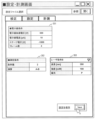
- FIG. 4 shows an example of a calibration screen on the setting and measurement screen.
- the user can input electron beam conditions 301, laser conditions 302, sample conditions 303, and calibration conditions 304 within the calibration screen.
- the user can set the electron beam acceleration voltage, electron beam current, stage voltage, and number of frames as the electron beam conditions 301 for calibration.
- the electron beam is a primary beam 251.
- the stage voltage is a voltage applied to the sample stage 108.
- the number of frames is a value indicating the number of frames used to generate an image of the sample, but if the output of the SEM 1 is not an image, it may be the irradiation time of the primary beam 251, etc.
- the control device 112 two-dimensionally scans the target area of the sample 200 with the primary beam 251 to generate an image.
- the average of four frames is the sample image.
- the detected signal amount may be, for example, the sum or average of the signal amounts of pixels of the image.
- Laser conditions 302 indicate conditions for the light source 103 and optical path 104.
- the wavelength and intensity of laser light can be set as the laser conditions 302.
- Sample condition 303 indicates the coordinates where a sample to be measured for calibration is placed.
- Calibration conditions 304 indicate the range of the EF voltage applied to the energy filter 116 and the set voltage V EF used in measuring the sample potential.
- the set voltage V EF is the final EF voltage obtained as a result of calibration.
- the user can set the sweep range of the EF voltage, and the set voltage VEF is calculated and set by the controller 112.
- the set voltage V EF may be input by the user according to the measurement results in the calibration.
- the user sets the EF voltage range of electron beam conditions 301, laser conditions 302, sample conditions 303, and calibration conditions 304 on the calibration screen.
- the control device 112 executes steps S11 to S14 in the flowchart of FIG.
- the control device 112 displays the detector characteristics 305 obtained through measurement on the calibration screen.
- the horizontal axis shows the EF voltage
- the vertical axis shows the detected signal amount of signal electrons. In a specific EF voltage range, the detected signal amount greatly decreases (increases) as the EF voltage increases (decreases).
- Controller 112 can determine the set voltage V EF based on the graph of detector characteristics 305 . Details of the method for determining the set voltage V EF will be described later.
- the set voltage V EF may be specified by the user. The user refers to the detector characteristics 305 and sets an EF voltage value that he considers appropriate to the cell of the set voltage VEF of the calibration condition 304.
- the set voltage V EF and other conditions 301 to 304 as well as the measurement results 305 of the detector characteristics are saved in the auxiliary storage device 123. At least some information other than the set voltage V EF may be excluded from the stored information.
- FIG. 5 shows a period of irradiation with ultraviolet laser light from the light source 103, a time change in the EF voltage, and a period of imaging (signal electron detection).
- the horizontal axis indicates time. Note that in this specification, both the acquisition of an image when the primary beam is scanned and the acquisition of signal electrons when the primary beam is maintained at one point are referred to as imaging.
- the control device 112 continues to irradiate the sample 200 with ultraviolet laser light during the measurement. That is, the light source 103 is kept ON during the measurement.
- the control device 112 sweeps the EF voltage from a low value to a high value while the sample 200 is irradiated with the laser beam. As shown in FIG. 5, the EF voltage is increased in steps.
- the control device 112 acquires an image of the sample 200. That is, the control device 112 scans a specific range on the sample 200 with the primary beam 251 to obtain an image of the sample 200. As described above, the control device 112 images a predetermined number of frames at each EF voltage value and generates an image based on the average value thereof. The control device 112 may determine the total or average value of the signal amount (brightness) of the pixels of the generated image as the detected signal amount of the signal electrons at the EF voltage.
- the ultraviolet laser light irradiation does not have to be always ON as in this embodiment. If the detection accuracy of signal electrons is degraded by irradiation with ultraviolet laser light, such as when photoelectrons are generated, it is effective to turn off the ultraviolet laser light in synchronization with the ON timing of imaging.
- FIG. 6 shows the detector characteristics.
- the detector characteristics are expressed by the relationship between the EF voltage and the detected signal amount of signal electrons.
- the horizontal axis shows the EF voltage, and the vertical axis shows the detected signal amount of signal electrons.
- the detected signal amount varies greatly within a specific EF voltage range. Specifically, the detected signal amount is approximately constant as the EF voltage increases from the lowest starting voltage to a specific EF voltage, but begins to decrease significantly at the specific EF voltage. The detected signal amount continues to decrease from the specific EF voltage to the specific EF voltage as the EF voltage increases, and thereafter remains approximately constant even if the EF voltage increases.
- the set voltage V EF may be set, for example, to an EF voltage value with the largest absolute value of the rate of change (differentiation) of the detected signal amount.
- FIG. 7 schematically shows the relationship between the EF voltage and the detection signal in different charging states of the sample.
- the horizontal axis shows the EF voltage
- the vertical axis shows the detected signal amount of signal electrons.
- a line 331 indicates the amount of detected signal for the uncharged sample
- a line 332 indicates the amount of detected signal for the charged sample.
- An uncharged sample corresponds to a sample that is measured while being irradiated with laser light for calibration.
- the charged sample corresponds to the sample to be measured.
- its detected signal amount begins to decrease at an EF voltage lower than that of an uncharged sample.
- a point 333A indicates the absolute value of the largest differential.
- Point 333B is a point having the same EF voltage as point 333A in the detected signal amount 332 of the charged sample. The detected signal amount at point 333B is smaller than the detected signal amount at point 333A.
- Point 333C is a point having the same detection signal amount as point 333B in the detection signal amount 331 of the uncharged sample. The EF voltage at point 333C is greater than the EF voltage at point 333B.
- the EF voltage at point 333A is the set voltage V EF at the time of sample measurement.
- the EF voltage difference ⁇ V between point 333C and point 333B indicates the potential difference between the charged sample and the uncharged sample.
- the difference between the set voltage V EF and the EF voltage of the uncharged sample at the detected signal amount of the sample to be measured is the potential difference between the sample to be measured and the uncharged sample.
- the potential difference from the sample potential of the uncharged sample indicates the amount of charge on the measurement sample.
- FIG. 8 shows the relationship between the detected signal amount of signal electrons and the sample potential, which is calculated as described above.
- the sample potential of the sample to be measured is expressed as a function of the amount of detected signal.
- Sample potential [V] f (signal electron detection signal amount)
- the control device 112 constructs conversion information that defines the function shown in FIG. 8 from the relationship 331 between the stage voltage and the EF voltage signal electron detection signal amount of the uncharged sample, which was measured in the calibration stage.
- the conversion information is information for converting the measurement result of the signal electrons of the sample (detected signal amount) into the sample potential, and can be expressed by a look-up table, a mathematical formula, or the like.
- the setting stage consists of step S15.
- the control device 112 sets measurement conditions for the target sample.
- FIG. 9 shows an example of a setting screen for measuring the film quality of the target sample.
- the user can set electron beam conditions 351, measurement conditions 352, and one or more laser conditions 353 corresponding to measurement conditions 352.
- the electron beam conditions 351 specify the primary electron beam, stage voltage, and number of frames, similar to the electron beam conditions 301 in the calibration stage.
- the measurement conditions 352 specify the number of sample measurement conditions and the calculation method for those measurement results.
- the user can specify multiple measurements under different conditions for one sample. In the example shown in FIG. 9, two measurement conditions A and B are specified, and the specified calculation method calculates the difference between the two measurement results.
- the user can specify the conditions for the laser light to be irradiated onto the sample.
- the laser light changes the potential of the sample as described above.
- the light source used for sample measurements may be the same or different from the laser used during the calibration stage.
- the irradiated light does not have to be laser light.
- the irradiated light may be, for example, a white light source such as a xenon lamp made monochromatic using a monochromator.
- FIG. 9 shows the laser conditions of measurement condition B (laser condition B) as an example.
- Laser conditions specify wavelength, intensity and polarization.
- Laser condition A specifies laser light with an intensity of 0, that is, non-irradiation of laser light.
- Laser condition B specifies irradiation with a laser beam having a wavelength of 350 nm, an intensity of 100 mW, and P polarization.
- Another example of two different measurement conditions A and B is that the measurement conditions A and B irradiate laser beams with different wavelengths.
- laser condition A is to irradiate a laser beam of 700 nm
- laser condition B is to irradiate a laser beam of 350 nm.
- the control device 112 calculates the difference between the detection signals at the two measurement stripes.
- the ultraviolet laser light under laser condition B acts on the insulating film using the static elimination effect, but at the same time it also acts on the underlying semiconductor, such as photovoltaic voltage.
- the energy of the signal electrons to be measured is a combination of the effects of the laser on the insulating film and the semiconductor. Since the near-infrared laser light under laser condition A passes through the insulating film, it acts only on the underlying silicon. That is, if the effect on the semiconductor cannot be ignored, the effect on the semiconductor is subtracted by calculating the difference between the measurement results under laser conditions A and B. Therefore, the effect on only the insulating film can be detected and the film quality such as the amount of charge of the insulating film can be appropriately measured.
- the number of measurement laser conditions specified in the measurement conditions 352 is not limited.
- the calculation method specified in the measurement conditions 352 is not limited to subtraction, and any suitable calculation method can be specified depending on the film quality to be calculated.
- FIG. 10 shows an example of a sequence of laser light irradiation and imaging under the setting conditions described with reference to FIG. 9.
- the control device 112 images the sample with the laser turned off (laser condition A) and acquires a signal 1A.
- the control device 112 images the sample in a state where the laser beam is irradiated (laser condition B) and obtains a signal 1B.
- control device 112 images the sample with the laser turned off (laser condition A) and acquires the signal 2A.
- the control device 112 images the sample in a state where the laser beam is irradiated (laser condition B) and obtains a signal 2B.
- control device 112 may determine the average value of the signal 1A and the signal 2A as the image acquired under laser condition A. Further, the control device 112 may determine the average value of the signal 1B and the signal 2B as the image acquired under the laser condition B.
- the measurement stage consists of steps S16 to S19.
- the control device 112 measures the target sample under laser condition A. As described above, under laser condition A, the sample is not irradiated with laser light.
- the control device 112 applies a set voltage V EF to the energy filter 116 without irradiating the laser beam.
- the control device 112 scans the specified region of the sample with the primary beam 252 under the conditions specified by the electron beam conditions 351. As a result, a two-dimensional sample image under laser condition A is obtained.
- step S17 the control device 112 measures the target sample under laser condition B.
- laser condition B specifies irradiation with a laser beam having a wavelength of 350 nm, an intensity of 100 mV, and P polarization.
- Controller 112 provides energy filter 116 with a set voltage V EF .
- the control device 112 scans the designated area of the sample with the primary beam 252 under the conditions specified by the electron beam conditions 351 while irradiating the sample with laser light under the specified conditions. As a result, a two-dimensional sample image under laser condition B is obtained.
- control device 112 may perform measurement (imaging) multiple times under each of the laser conditions A and B, or the number of measurements under each of the laser conditions A and B. may occur only once.
- step S18 the control device 112 determines the sample potential under laser condition A based on the detected signal amount under laser condition A with reference to the conversion information. Furthermore, the control device 112 determines the sample potential under laser condition B based on the detected signal amount under laser condition B and with reference to the conversion information.
- the control device 112 calculates the sample potential change under laser condition A and laser condition B. Using the relationship shown in FIG. 8, a value obtained by subtracting the sample potential under laser condition B from the sample potential under laser condition A is calculated. Note that the control device 112 calculates the difference between the detected signal amount under laser condition A and the detected signal amount under laser condition B, and determines the potential change between the two laser conditions based on the difference and conversion information. You can.
- the difference in detected signal amount and potential change between condition A and condition B are comparison signals representing the comparison results of detected signal amount under these conditions.
- step S19 the control device 112 calculates the film quality according to the calculation method specified by the measurement conditions 352 shown in FIG. 9, and outputs the result.
- the control device 112 subtracts the sample potential under laser condition B from the sample potential under laser condition A according to the measurement conditions specified on the setting screen, and uses the difference as information representing the film quality of the insulating film. Output to the output device 124.
- FIG. 11 shows an example of a GUI screen for the measurement stage.
- the user can specify the coordinates 381 of the measurement target.
- the designated coordinates may be, for example, a reference position of a predetermined scanning area or a position of a point irradiated with the primary beam.
- the user can specify the membrane mass 382 to be displayed.
- the voltage of the sample is specified.
- the amount of charge on the insulating film calculated as described above is displayed.
- the amount of charge is an example of a numerical value representing a change in sample potential.
- the control device 112 may hold reference information for calculating the membrane mass in another designated unit from the calculated sample potential. Thereby, the membrane mass can be displayed in units selected from a plurality of options.
- the measurement GUI screen further shows the measurement results of the sample.
- an SEM image 383 as a comparison target is displayed. This allows the user to visually check the film quality of the target sample in comparison with the structure.
- the measurement area of the sample is composed of, for example, a silicon line 391 and an insulating film 392 formed on silicon in a trench portion between the silicon lines 391.
- the film quality image 384 shows the distribution of the difference between the sample potential under laser condition A and the sample potential under laser condition B in the measurement region.
- the film quality image 384 shows that the amount of charge on the insulating film 392 varies depending on the distance from silicon.
- the amount of charge represents the quality of the insulating film 392.
- FIG. 12 shows another example of the GUI screen for the measurement stage. Compared to the GUI screen example shown in FIG. 11, the displayed measurement results are different.
- the GUI screen in FIG. 12 shows a wafer heat map 387 as a measurement result.
- each measurement result indicates one value.
- the control device 112 can create and display a wafer heat map 387, which is a heat map of the film quality on the wafer.
- the electron beam current is large in the condition setting of S15, the charge on the insulating film is saturated, and the measured charge amount means the withstand voltage of the insulating film. That is, the withstand voltage can also be measured in the same way.
- FIG. 13 shows an example of the device configuration of the SEM 2 equipped with a lock-in detection mechanism. Measurement sensitivity can be improved by using a lock-in detection mechanism.
- SEM2 includes a lock-in amplifier 113 in addition to the components of SEM1 shown in FIG.
- the control device 112 modulates the intensity of the light source 103 at a constant cycle and provides a reference signal with the same cycle to the lock-in amplifier 113.
- the lock-in amplifier 113 enables highly accurate detection by the detector 110 which is modulated in synchronization with this period.
- lock-in detection is particularly effective when the calculation specified by the measurement condition 352 is to calculate the difference between detection signals obtained under two laser conditions.
- Lock-in detection allows the controller 112 to make more accurate and faster measurements than subtraction.
- Example 3 of this specification SEM processing according to Example 3 of this specification will be described below. In the following, differences from Example 1 will be mainly explained.
- the configuration of the SEM of this embodiment may be the same as that of the first embodiment.
- the amount of charge or withstand voltage of the insulating film is presented to the user as a physical quantity (material characteristic value) representing the film quality.
- the control device 112 uses user input to measure and present defect density, which is an example of another physical quantity representing film quality. This embodiment enables accurate defect density measurement.
- FIG. 14 shows a flowchart of an example of control processing of the SEM 1 by the control device 112 in this embodiment. Steps S11 to S18 are similar to steps S11 to S18 in the flowchart of FIG. 3 of the first embodiment.
- step S31 the control device 112 acquires information about the membrane to be measured (membrane information) that has been input in advance by the user.
- the film information is stored in the auxiliary storage device 123, for example.
- the film information can include, for example, film thickness, dielectric constant, and the like.
- step S32 the control device 112 calculates the film quality of the measurement target, in this case the defect density, based on the comparison results of sample potentials (detection signal amount) under different laser conditions and the film information, and Output to the output device 124.
- the control device 112 can calculate the defect density using a preset film quality conversion formula.
- V is the sample potential difference under laser condition A and laser condition B, and is obtained by measurement.
- the control device 112 converts the comparison result of the measured sample potential into a film quality value of defect density using the film information and conversion formula input by the user, and outputs the result.
- the film information includes the dielectric constant ⁇ r and the film thickness d of the insulating film to be measured.
- FIG. 15 shows an example of the GUI screen at the measurement stage.
- the user can input information necessary to measure desired film quality on the GUI screen. Specifically, information about the membrane to be measured and a conversion formula for calculating a desired physical quantity representing the membrane quality can be input. Further, the GUI screen presents the measurement results of the film quality of the sample to the user.
- the user specifies, in addition to measurement coordinates 381, information 401 on the membrane mass to be measured and displayed.
- the membrane mass information 401 specifies a physical quantity to be measured and displayed, membrane information, and a conversion formula for calculating the physical quantity.
- defect density density of material defects
- the film information indicates the film thickness and dielectric constant.
- the user can input a conversion formula into the conversion formula cell. Alternatively, if a simple assumption such as the above conversion formula 2 is sufficient, the control device 112 holds it as default information, and the user can simply select it.
- the measurement GUI screen displays a wafer heat map 402 to the user as a measurement result.
- the wafer heat map 402 is a map showing the relationship between the position on the wafer and the measured defect density.
- the wafer heat map 402 can be created in the same way as the wafer heat map 387 shown in FIG.
- a film quality image indicating defect density may be generated and displayed, such as a film quality image 384 shown in FIG. 11 .
- Example 4 of this specification SEM processing according to Example 4 of this specification will be described below. In the following, differences from Example 1 will be mainly explained.
- the configuration of the SEM of this embodiment may be the same as that of the first embodiment.
- the control device 112 measures and presents defect levels and band energy levels, which are examples of physical quantities representing the film quality of the insulating film.
- defect levels and band energy levels are examples of physical quantities representing the film quality of the insulating film.
- the control device 112 measures the energy level (film quality) from the dependence of the insulating film voltage on the wavelength of light. To measure energy levels, it is necessary to measure the voltage across the insulating film at multiple wavelengths.
- An example of measuring the energy level of an important band in a semiconductor device is measuring the energy level difference between the valence band of a semiconductor and the conduction band of an insulating film. This energy level difference can be determined by measuring the energy required to inject electrons within the semiconductor into the insulating film. Electrons in a semiconductor are excited by absorbing light and gain energy equal to the energy of photons.
- the level energy difference can be calculated by measuring the wavelength of light having a photon energy that can eliminate static electricity from the insulating film.
- the energy level is calculated from the relationship between the insulating film voltage and the wavelength (photon energy) of the irradiated light.
- the control device 112 may control the laser light source 103 so that the number of photons per unit time is the same between wavelengths.
- the number of photons per second is the laser energy divided by the photon energy per second.
- FIG. 16 shows a flowchart of an example of control processing of the SEM 1 by the control device 112 in this embodiment. Steps S11 to S18 are similar to steps S11 to S18 in the flowchart of FIG. 3 of the first embodiment.
- the control device 112 changes either or both of the wavelengths of the laser light irradiated to the sample set under laser condition A and laser condition B (S41), and repeats the loop from steps S16 to S18 with a different laser light wavelength. For example, the wavelength of laser condition B in FIG. 10 is changed. After that, in step S42, the control device 112 determines the energy level from the measurement result of the relationship between the sample potential and the photon energy. The photon energy, which varies greatly in sample potential, determines the energy level difference.
- FIG. 17 shows an example of the GUI screen at the measurement stage.
- the user can input information necessary to measure desired film quality on the measurement GUI screen.
- the energy level is selected as the physical quantity to display the film quality.
- the measurement GUI screen further presents the measurement results of the film quality of the sample to the user.
- the user specifies the membrane mass information 411 to be displayed in addition to the measurement coordinates 381.
- the film mass information 411 specifies an energy level as a physical quantity representing film quality.
- the measurement GUI screen shows a graph 412 showing the relationship between photon energy and sample potential change between conditions A and B as a measurement result.
- the horizontal axis represents photon energy and the vertical axis represents sample voltage.
- the sample potential is the same under laser condition A and laser condition B, so the sample potential change is low and approximately constant.
- static elimination occurs at a specific photon energy, the sample potential measured under laser condition A and laser condition B differs, and the sample potential change starts to increase.
- the sample potential change is approximately constant as the static elimination effect is saturated in the high photon energy region.
- the control device 112 determines the intersection of the tangent to the point where the sample voltage changes the most with respect to a change in photon energy, that is, the point where the absolute value of the differential is the largest, and the approximate straight line in the low photon energy region. It may be determined as an energy level.
- the measurement GUI screen further displays a wafer heat map 413 to the user.
- the wafer heat map 413 is a map showing the relationship between positions on the wafer and measured energy levels.
- the wafer heat map 413 can be created in the same manner as the wafer heat map 387 shown in FIG.
- a film quality image showing the energy level may be generated and displayed, such as a film quality image 384 shown in FIG. 11 .
- the energy level difference between the semiconductor and the insulating film was measured. If the energy level of one side, for example a semiconductor, is known as an absolute value, the energy level of the insulating film can be determined using the measured energy level difference. In addition, if there are traps in the insulating film or its interface, it is possible to excite the electrons held in the traps with light, and similarly to the band energy level difference between the semiconductor and the insulating film, the amount of sample potential change and the photon The trap level can be determined from the energy relationship.
- Example 5 of this specification SEM processing according to Example 5 of this specification will be described below. In the following, differences from Example 1 will be mainly explained.
- the configuration of the SEM of this embodiment may be the same as that of the first embodiment.
- the control device 112 measures and presents carrier life and mobility, which are examples of physical quantities representing film quality. This embodiment enables accurate measurement of carrier lifetime and mobility.
- the control device 112 measures carrier life and mobility from the time difference between pulsed light irradiation and pulsed electron beam (primary beam) irradiation. Carrier lifetime and mobility appear in the transient response of measurements.
- FIG. 18 shows an example of a sequence of laser beam irradiation and imaging (primary beam irradiation) on a sample.
- the control device 112 images the sample with the laser turned off (laser condition A) and acquires the signal 1A.
- the control device 112 images the sample after a predetermined waiting time (DELAY) and acquires the signal 1B.
- DELAY waiting time
- signal 1A and signal 1B are acquired.
- Signals 2A, 2B are then obtained by measurements at different latencies. Thereafter, measurements are repeated with different waiting times.
- the control device 112 does not acquire the signal 1B by simultaneous irradiation with a laser beam and an electron beam (primary beam), but instead sets a time difference (DELAY) between the laser beam irradiation and the electron beam irradiation. establish.
- the control device 112 can measure the response of the insulating film and its interface to light by controlling the length of the waiting time and measuring the dependency of the measured potential change on the waiting time.
- the control device 112 uses a conversion formula to convert the response characteristics into carrier lifetime and mobility.
- This conversion formula takes waiting time as a factor. For example, carrier life and mobility can be calculated from the waiting time at which the sample potential changes significantly using a conversion formula.
- FIG. 19 shows an example of a sequence of laser beam irradiation to a sample and imaging (primary beam irradiation).
- the control device 112 images the sample and acquires the signal 1A without irradiating the sample with laser light (laser 1 condition A and laser 2 condition A).
- the control device 112 controls the sample while irradiating laser beam 2 (laser 2 condition B). Imaging is performed and signal 1B is acquired. In one measurement, signal 1A and signal 1B are acquired. Signals 2A, 2B are then obtained by measurements at different latencies. Thereafter, measurements are repeated with different waiting times.
- the control device 112 can calculate and output the response characteristic of the phenomenon from the relationship between the sample potential change and the waiting time.
- the waiting time (time difference) can be input as a set value by the user on the measurement GUI screen.
- the control device 112 can display, as a measurement result, a graph in which the horizontal axis indicates the waiting time and the vertical axis indicates the sample potential change.
- a heat map or film quality image indicating carrier life and mobility may be generated and displayed.
- FIG. 20 shows an example of the GUI screen at the measurement stage.
- the user can input information necessary to measure desired film quality on the measurement GUI screen.
- carrier life is selected as the physical quantity to display film quality.
- the measurement GUI screen further presents the measurement results of the film quality of the sample to the user.
- the user specifies the membrane mass information 411 to be displayed in addition to the measurement coordinates 381.
- the film mass information 411 specifies carrier life as a physical quantity representing film quality.
- the measurement GUI screen shows a graph 432 showing the relationship between waiting time and sample potential change between conditions A and B as a measurement result.
- the horizontal axis shows waiting time and the vertical axis shows sample voltage.
- the control device 112 determines the intersection of the tangent to the point where the sample voltage changes the most with respect to a change in the waiting time, that is, the point where the absolute value of the differential is the largest, and the approximate straight line in the region of the large waiting time. may be determined to have a career life of .
- the measurement GUI screen further displays a wafer heat map 433 to the user.
- the wafer heat map 433 is a map showing the relationship between the position on the wafer and the measured carrier life.
- the wafer heat map 413 can be created in the same way as the wafer heat map 387 shown in FIG.
- a film quality image indicating the carrier life may be generated and displayed, such as a film quality image 384 shown in FIG. 11 .
- the present invention is not limited to the above-described embodiments, and includes various modifications.
- the embodiments described above are described in detail to explain the present invention in an easy-to-understand manner, and the present invention is not necessarily limited to having all the configurations described.
- it is possible to replace a part of the configuration of one embodiment with the configuration of another embodiment and it is also possible to add the configuration of another embodiment to the configuration of one embodiment.
- each of the configurations, functions, processing units, etc. described above may be partially or entirely realized in hardware by, for example, designing an integrated circuit.
- each of the above-mentioned configurations, functions, etc. may be realized by software by a processor interpreting and executing a program for realizing each function.
- Information such as programs, tables, files, etc. that implement each function can be stored in a memory, a recording device such as a hard disk, an SSD (Solid State Drive), or a recording medium such as an IC card or an SD card.
- control lines and information lines are shown that are considered necessary for explanation, and not all control lines and information lines are necessarily shown in the product. In reality, almost all configurations may be considered interconnected.
Abstract
This sample measuring device comprises: a light source that irradiates a sample including an insulating film with light; an excitation source that irradiates the sample with a primary beam to emit charged particles; a detector that applies at least one of an electric field or a magnetic field to the charged particles to separate the trajectories in accordance with the energy of the charged particles, and outputs a detection signal that depends on the energy of the charged particles; and a control device that processes the detection signal of the charged particles obtained from the detector. The control device changes a light irradiation condition, acquires a detection signal by the detector under a different irradiation condition, and determines and outputs material characteristic values from the detection signal under the different irradiation condition by using information indicating the relationship between the detection signal and the material characteristic values of the insulating film.
Description
本発明は試料測定装置に関する。
The present invention relates to a sample measuring device.
半導体デバイスにおいて、絶縁膜の膜質は重要である。ここでは、絶縁膜または絶縁膜と半導体界面の欠陥(トラップ)密度、欠陥準位、バンドエネルギ、キャリア移動度、キャリア寿命や絶縁膜に印加できる最大電圧(耐電圧)を含む材料特性等の物性を総じて膜質と呼ぶ。膜質の重要な絶縁膜の一つにトランジスタのゲート酸化膜がある。ゲート酸化膜に欠陥が多く存在し膜質が悪い場合、時間とともに絶縁膜に電荷がたまりトランジスタの性能を変化させてしまう。すなわち、デバイスの信頼性を低下する。また、メモリデバイスにおいても絶縁膜は電荷を保持することでメモリ機能として使う重要な膜である。この場合も、絶縁膜の膜質はメモリの揮発性等、メモリとしての機能を左右する。このように、デバイスに重要な絶縁膜の膜質は半導体プロセス中に適時検査及び計測することによって半導体デバイスの歩留まりや信頼性を向上することができる。
In semiconductor devices, the quality of the insulating film is important. Here, physical properties such as defect (trap) density, defect level, band energy, carrier mobility, carrier lifetime, and material properties of the insulating film or the interface between the insulating film and the semiconductor, including the maximum voltage (withstanding voltage) that can be applied to the insulating film, are discussed. are collectively called membranous. One of the insulating films whose film quality is important is the gate oxide film of a transistor. If the gate oxide film has many defects and is of poor quality, charge accumulates in the insulating film over time, changing the performance of the transistor. That is, it reduces the reliability of the device. Furthermore, in memory devices, insulating films are also important films used for memory functions by retaining charge. In this case as well, the film quality of the insulating film influences the functionality of the memory, such as the volatility of the memory. In this way, the yield and reliability of semiconductor devices can be improved by timely inspecting and measuring the quality of the insulating film, which is important for devices, during the semiconductor process.
特許文献1には、半導体試料に光を照射することで生じる試料表面での電位の変化を電子線で測定する装置が記載されている。
Patent Document 1 describes an apparatus that uses an electron beam to measure changes in potential on the surface of a semiconductor sample caused by irradiating the sample with light.
膜質を測る手法として、対象とする絶縁膜を電極で挟んだ時の容量と電圧の関係を測るCV測定が知られている。しかし、CV測定は、絶縁膜上に電極を作製する必要があり、時間とコストをともなう。また、電極を小さく作るのは難しく、膜質測定の空間分解能は限られている。微細な半導体デバイスを完成していない絶縁膜成膜直後の状態からでも高い空間分解能で絶縁膜質を検査計測する手法が求められる。
CV measurement, which measures the relationship between capacitance and voltage when a target insulating film is sandwiched between electrodes, is known as a method for measuring film quality. However, CV measurement requires forming electrodes on an insulating film, which is time consuming and costly. Furthermore, it is difficult to make small electrodes, and the spatial resolution of film quality measurements is limited. There is a need for a method that can inspect and measure the quality of an insulating film with high spatial resolution even immediately after the insulating film has been deposited, even before microscopic semiconductor devices have been completed.
特許文献1に記載の装置は、電子線によって帯電しない半導体の特性を評価する。絶縁体は電子線によって帯電し、評価する物性も異なるため特許文献1の装置では不十分である。
The device described in Patent Document 1 evaluates the characteristics of a semiconductor that is not charged by an electron beam. The device of Patent Document 1 is insufficient because the insulator is charged by the electron beam and the physical properties to be evaluated are different.
本発明の一態様の試料測定装置は、絶縁膜を含む試料に光を照射する光源と、一次ビームを前記試料に照射して、荷電粒子を放出させる、励起源と、前記荷電粒子に電場又は磁場の少なくても一つを印加して前記荷電粒子のエネルギに応じて軌道を分離することにより、前記荷電粒子のエネルギに依存する検出信号を出力する検出器と、前記検出器から得られる前記荷電粒子の検出信号を処理する制御装置と、ユーザから前記試料に関する情報を入力する入力装置と、を含み、前記制御装置は、前記光の異なる照射条件で前記検出器により検出された検出信号と、前記検出信号と前記試料の電位との関係を示す情報に基づき、前記異なる照射条件での前記試料の電位変化を決定し、前記試料に関する情報に含まれる膜厚及び誘電率を用いて、前記電位変化を前記絶縁膜の材料特性値に換算して出力する。
A sample measuring device according to one aspect of the present invention includes a light source that irradiates a sample including an insulating film with light, an excitation source that irradiates the sample with a primary beam to emit charged particles, and an electric field or a detector for outputting a detection signal dependent on the energy of the charged particles by applying at least one magnetic field to separate the trajectories depending on the energy of the charged particles; The control device includes a control device that processes a detection signal of charged particles, and an input device that inputs information regarding the sample from a user, and the control device processes a detection signal detected by the detector under different irradiation conditions of the light. , determining the potential change of the sample under the different irradiation conditions based on information indicating the relationship between the detection signal and the potential of the sample, and using the film thickness and dielectric constant included in the information regarding the sample, The potential change is converted into a material characteristic value of the insulating film and output.
本発明の一態様の試料測定装置は、絶縁膜を含む試料に複数の波長の光を照射する光源と、一次ビームを前記試料に照射して、荷電粒子を放出させる、励起源と、前記荷電粒子に電場又は磁場の少なくても一つを印加して前記荷電粒子のエネルギに応じて軌道を分離することにより、前記荷電粒子のエネルギに依存する検出信号を出力する検出器と、前記検出器から得られる前記荷電粒子の検出信号を処理する制御装置と、を含み、前記制御装置は、前記光の異なる波長のそれぞれにおいて、前記光の異なる照射条件で前記検出器により検出された検出信号の比較結果を示す比較信号を生成し、前記比較信号に基づく前記絶縁膜の膜質の情報を出力する。
A sample measuring device according to one aspect of the present invention includes: a light source that irradiates a sample including an insulating film with light of a plurality of wavelengths; an excitation source that irradiates the sample with a primary beam to emit charged particles; a detector that outputs a detection signal that depends on the energy of the charged particle by applying at least one of an electric field or a magnetic field to the particle to separate trajectories according to the energy of the charged particle; a control device for processing a detection signal of the charged particles obtained from the detector, the control device processing the detection signal detected by the detector under different irradiation conditions of the light at each of the different wavelengths of the light. A comparison signal indicating a comparison result is generated, and information on the film quality of the insulating film based on the comparison signal is output.
本発明の一態様の試料測定装置は、絶縁膜を含む試料に光を照射する光源と、一次ビームを前記試料に照射して、荷電粒子を放出させる、励起源と、前記荷電粒子に電場又は磁場の少なくても一つを印加して前記荷電粒子のエネルギに応じて軌道を分離することにより、前記荷電粒子のエネルギに依存する検出信号を出力する検出器と、前記検出器から得られる前記荷電粒子の検出信号を処理する制御装置と、ユーザから前記試料に関する情報を入力する入力装置と、を含み、前記制御装置は、前記光の照射条件を変えて、異なる照射条件で前記検出器により検出信号を取得し、前記検出信号と前記絶縁膜の材料特性値との関係を示す情報を用いて、前記異なる照射条件での検出信号から前記材料特性値を決定して出力する。
A sample measuring device according to one aspect of the present invention includes a light source that irradiates a sample including an insulating film with light, an excitation source that irradiates the sample with a primary beam to emit charged particles, and an electric field or a detector for outputting a detection signal dependent on the energy of the charged particles by applying at least one magnetic field to separate the trajectories depending on the energy of the charged particles; The control device includes a control device that processes a detection signal of charged particles, and an input device that inputs information about the sample from a user, and the control device changes the light irradiation conditions and performs the detection using the detector under different irradiation conditions. A detection signal is acquired, and using information indicating a relationship between the detection signal and the material characteristic value of the insulating film, the material characteristic value is determined and output from the detection signal under the different irradiation conditions.
本発明の一態様によれば、試料の所望の膜質を測定することができる。
According to one aspect of the present invention, desired film quality of a sample can be measured.
以下、図面を用いて実施例を説明する。なお、実施例を説明するための全図において、同一の要素には同一の符号を付し、その繰り返しの説明は省略される。以下において具体的に説明される装置の例は、一次ビームとして電子ビームを使用して、信号荷電粒子として信号電子を検出することにより、試料を測定する。本開示の特徴は、他の装置、例えば、一次ビームとしてイオンビーム又はレーザ光を使用し及び/または信号荷電粒子としてイオンを検出するする装置にも適用できる。
Examples will be described below with reference to the drawings. In addition, in all the figures for explaining the embodiment, the same elements are given the same reference numerals, and repeated explanations thereof will be omitted. The example apparatus specifically described below measures a sample by using an electron beam as the primary beam and detecting the signal electrons as the signal charged particles. Features of the present disclosure are also applicable to other devices, such as those that use ion beams or laser light as the primary beam and/or detect ions as signal charged particles.
図1は、走査電子顕微鏡装置(SEM)1の概略構成例を模式的に示す。走査電子顕微鏡装置1は、試料の膜質の材料特性値、例えば、絶縁膜の電位や耐電圧を測定する、本明細書の一実施例に係る試料測定装置である。SEM1は、電子ビームを使用して、試料の観察及び測定を行う。
FIG. 1 schematically shows an example of a schematic configuration of a scanning electron microscope (SEM) 1. The scanning electron microscope device 1 is a sample measuring device according to an embodiment of the present specification that measures material characteristic values of the film quality of a sample, such as the potential and withstand voltage of an insulating film. The SEM 1 uses an electron beam to observe and measure a sample.
図1に示すSEM1は、電子光学系と、電子光学系を制御し、試料を測定する制御装置112と、を含む。説明の容易のため、図1は、電子光学系の一部の構成要素のみを示す。SEMは図示されていない他の構成要素、例えば、他のレンズ、アライナ、スティグメータ、偏向器やセパレータ等が付加されてもよい。SEMの光学素子(レンズ、偏向器、セパレータ等)は、電場、磁場、又は磁場及び電場の複合を生成し、電子ビームに対して作用を及ぼす。
The SEM 1 shown in FIG. 1 includes an electron optical system and a control device 112 that controls the electron optical system and measures a sample. For ease of explanation, FIG. 1 shows only some components of the electron optical system. Other components not shown in the drawings may be added to the SEM, such as other lenses, aligners, stigmators, deflectors, and separators. The optical elements of a SEM (lenses, deflectors, separators, etc.) generate electric fields, magnetic fields, or a combination of magnetic and electric fields and act on the electron beam.
電子光学系において、励起源101から試料200へ向けて引き出された一次ビーム251の軌道上に、対物レンズ107が配置されている。本例において、励起源101は(電子源であるが、信号荷電粒子を放出する励起源であれば他の荷電粒子原又はレーザ等が使用されてもよい)。
In the electron optical system, an objective lens 107 is placed on the trajectory of the primary beam 251 extracted from the excitation source 101 toward the sample 200. In this example, the excitation source 101 is an electron source (although any other charged particle source, laser, etc. may be used as long as it is an excitation source that emits signal charged particles).
一次ビーム251は、対物レンズ107を通過した後に、試料200上で集束される。例えば、不図示の走査用偏向器が励起源101と対物レンズ107との間に配置され、一次ビーム251が試料200上の領域を二次元的に走査するように、一次ビーム251の向きを制御する。
The primary beam 251 is focused on the sample 200 after passing through the objective lens 107. For example, a scanning deflector (not shown) is placed between the excitation source 101 and the objective lens 107, and the direction of the primary beam 251 is controlled so that the primary beam 251 scans an area on the sample 200 two-dimensionally. do.
試料200に照射された一次ビーム251は表面付近の物質と相互に作用し、試料の形状や材料に応じて二次電子やそれ以外の信号電子が発生する。本実施例では、試料200から放出され検出器110で検出される二次電子を信号電子と呼ぶ。
The primary beam 251 irradiated onto the sample 200 interacts with substances near the surface, and secondary electrons and other signal electrons are generated depending on the shape and material of the sample. In this embodiment, the secondary electrons emitted from the sample 200 and detected by the detector 110 are called signal electrons.
試料200は、ステージ108の上に配置されている。試料200に照射された一次ビーム251は、試料200の表面付近の物質と相互に作用し、信号電子261を生成する。ステージ108には負電圧が印加されており、試料200上には電界が生成されている。この電界により信号電子261は、一次ビーム251の軌道を逆戻りする。不図示のビームセパレータは、信号電子261を偏向させて、それらの軌道を一次ビーム251の軌道から分離させる。
The sample 200 is placed on the stage 108. The primary beam 251 irradiated onto the sample 200 interacts with substances near the surface of the sample 200 to generate signal electrons 261 . A negative voltage is applied to the stage 108, and an electric field is generated on the sample 200. This electric field causes the signal electrons 261 to reverse the trajectory of the primary beam 251. A beam separator, not shown, deflects the signal electrons 261 to separate their trajectory from that of the primary beam 251.
検出器110は、信号電子261を検出し、検出信号に変換する。検出信号の強度は、一次ビーム251が照射する位置での試料200の形状や材質に応じて変化する。
The detector 110 detects the signal electron 261 and converts it into a detection signal. The intensity of the detection signal changes depending on the shape and material of the sample 200 at the position irradiated with the primary beam 251.
エネルギフィルタ(EF)116は、検出器110の前に配置されている。エネルギフィルタ116と検出器110とは、エネルギ検出器106を構成する。試料200からの信号電子261は、エネルギフィルタ116を通過して、検出器110に入射する。検出器110は、エネルギフィルタ116を通過した信号電子261を検出する。エネルギフィルタ116は、EF電源111に接続されている。EF電源111は、制御装置112により設定された電圧をエネルギフィルタ116に与える。
An energy filter (EF) 116 is placed in front of the detector 110. Energy filter 116 and detector 110 constitute energy detector 106. Signal electrons 261 from the sample 200 pass through the energy filter 116 and enter the detector 110. Detector 110 detects signal electrons 261 that have passed through energy filter 116. Energy filter 116 is connected to EF power supply 111. EF power supply 111 provides a voltage set by control device 112 to energy filter 116 .
エネルギフィルタ116は、例えば、金属メッシュを含み、EF電源111からの電圧が印加される。エネルギフィルタ116は、印加されているEF電圧に応じて、信号電子261を跳ね返す又は通過させる。このように、エネルギフィルタ116は、信号電子261のエネルギに応じて軌道を分離する。
The energy filter 116 includes, for example, a metal mesh, and a voltage from the EF power supply 111 is applied thereto. Energy filter 116 either reflects or passes signal electrons 261 depending on the EF voltage being applied. In this way, the energy filter 116 separates the orbits of the signal electrons 261 according to their energy.
エネルギフィルタ116は電場によって、信号電子261の軌道をそのエネルギに応じて分離する。他例のエネルギフィルタは、磁場によって、信号電子261の軌道をそのエネルギに応じて分離してもよい。また、エネルギフィルタは信号電子を反射せずエネルギに応じて異なる角度で偏向し信号電子を軌道分離するスペクトロメータでもよい。エネルギ検出器は、信号電子に電場又は磁場の少なくても一つを印加して信号電子のエネルギに応じてその軌道を分離することにより信号電子のエネルギに依存する検出信号を出力できる。
The energy filter 116 uses an electric field to separate the orbits of the signal electrons 261 according to their energies. Another example of an energy filter may use a magnetic field to separate the trajectory of the signal electron 261 according to its energy. Alternatively, the energy filter may be a spectrometer that does not reflect the signal electrons but deflects them at different angles depending on the energy to separate the signal electrons into orbits. The energy detector can output a detection signal that depends on the energy of the signal electrons by applying at least one of an electric field or a magnetic field to the signal electrons to separate their orbits according to the energy of the signal electrons.
制御装置112は、EF電圧をスイープして、信号電子261が検出器110によって検出できなくなる又は検出可能となるEF電圧を決定する。信号電子261の検出の有無を示すEF電圧は、信号電子261のエネルギに対応しており、信号電子261のエネルギは、試料200の電位と対応付けられる。
The controller 112 sweeps the EF voltage and determines the EF voltage at which the signal electrons 261 become undetectable or detectable by the detector 110. The EF voltage indicating whether or not the signal electron 261 is detected corresponds to the energy of the signal electron 261, and the energy of the signal electron 261 is associated with the potential of the sample 200.
試料200は絶縁体を含むため、一次ビーム251の照射により帯電する。例えば、試料200が正に帯電しているものとする。試料200の電位が高い場合、検出される信号電子261のエネルギは低くなる。例えば、試料200が無帯電の状態において、信号電子261のエネルギが1kVとして、正帯電の状態において、信号電子261は、990Vの運動エネルギを有し得る。
Since the sample 200 includes an insulator, it is charged by irradiation with the primary beam 251. For example, assume that the sample 200 is positively charged. When the potential of the sample 200 is high, the energy of the detected signal electrons 261 is low. For example, if the energy of the signal electrons 261 is 1 kV when the sample 200 is uncharged, the signal electrons 261 may have a kinetic energy of 990 V when the sample 200 is positively charged.
検出器110は、信号電子エネルギを測定する。後述するように、検出器110による信号電子エネルギの測定結果に基づいて、試料200の電位及びそれに基づく試料の膜質が測定される。測定される膜質は、例えば、絶縁膜内又は界面の、欠陥密度[個/cm2]、キャリア移動度[cm2/(Vs)]、欠陥準位[eV]又はバンドエネルギ[eV]等である。絶縁膜の欠陥は、形状欠陥ではなく、トラップ等の材料欠陥である。
Detector 110 measures the signal electronic energy. As will be described later, the potential of the sample 200 and the film quality of the sample based on the potential of the sample 200 are measured based on the measurement results of the signal electron energy by the detector 110. The film quality to be measured is, for example, defect density [pieces/cm 2 ], carrier mobility [cm 2 /(Vs)], defect level [eV], or band energy [eV] in the insulating film or at the interface. be. Defects in the insulating film are not shape defects but material defects such as traps.
より正確な測定のためには、試料200が無帯電の状態での、信号電子エネルギを知ることが重要である。本明細書の一実施例のSEM1は、光源103からの光105を試料200に照射することで、試料200を除電する。制御装置112は、光源103及び/又は光路104を制御し、光路104を介して、光105を試料200に照射する。光105は、例えば、紫外光であり、その波長は例えば波長400nm以下であってよい。光源103は、例えば、紫外光レーザである。光源103は白色光源をモノクロメータで単色化したものでもよい。また、光源103は複数の光源から構成され、波長設定に応じて光源を選択する構成でもよい。
For more accurate measurements, it is important to know the signal electron energy when the sample 200 is uncharged. The SEM 1 according to the embodiment of this specification removes static electricity from the sample 200 by irradiating the sample 200 with light 105 from the light source 103. The control device 112 controls the light source 103 and/or the optical path 104, and irradiates the sample 200 with light 105 via the optical path 104. The light 105 is, for example, ultraviolet light, and its wavelength may be, for example, 400 nm or less. The light source 103 is, for example, an ultraviolet laser. The light source 103 may be a white light source made monochromatic using a monochromator. Further, the light source 103 may be composed of a plurality of light sources, and the light source may be selected according to the wavelength setting.
例えば、制御装置112は、光源103からの紫外光105を試料200に照射した状態で、EF電圧と信号電子エネルギとの関係を測定する。これにより、試料200の帯電量が0Vでの、信号電子261のエネルギが分かる。その後、制御装置112は、光源103または光路104で光105をOFFに維持して、EF電圧と信号電子エネルギとの関係を測定する。二つの測定結果から、一次ビーム251を試料200に照射した時の試料200の帯電量[V]が分かる。
For example, the control device 112 measures the relationship between the EF voltage and the signal electron energy while the sample 200 is irradiated with the ultraviolet light 105 from the light source 103. As a result, the energy of the signal electrons 261 when the amount of charge on the sample 200 is 0V can be determined. Thereafter, the controller 112 keeps the light 105 OFF in the light source 103 or optical path 104 and measures the relationship between the EF voltage and the signal electron energy. From the two measurement results, the amount of charge [V] of the sample 200 when the sample 200 is irradiated with the primary beam 251 can be determined.
測定のための電子光学系の上記全ての構成要素は、制御装置112によって制御される。図1の構成例において、制御装置112は、制御演算部114及び入出力部115を含む。制御演算部114は、各構成要素を制御すると共に、検出器110により検出された信号電子強度を演算し、所望の情報を生成する。入出力部115は、ユーザによる設定操作を受け付けると共に、ユーザに対して要求された情報を提示する。
All the above components of the electron optical system for measurement are controlled by a control device 112. In the configuration example of FIG. 1, the control device 112 includes a control calculation section 114 and an input/output section 115. The control calculation unit 114 controls each component, calculates the signal electron intensity detected by the detector 110, and generates desired information. The input/output unit 115 accepts setting operations by the user and presents requested information to the user.
図2は、制御装置112のハードウェア構成例を示す。制御装置112は、計算機構成を有することができる。制御装置112は、プロセッサ121、メモリ(主記憶装置)122、補助記憶装置123、出力装置124、入力装置125、及び通信インタフェース(I/F)127を含む。上記構成要素は、バスによって互いに接続されている。メモリ122、補助記憶装置123又はこれらの組み合わせは記憶装置であり、プロセッサ121が使用するプログラム及びデータを格納している。
FIG. 2 shows an example of the hardware configuration of the control device 112. Control device 112 can have a computer configuration. The control device 112 includes a processor 121 , a memory (main memory) 122 , an auxiliary memory 123 , an output device 124 , an input device 125 , and a communication interface (I/F) 127 . The above components are connected to each other by a bus. Memory 122, auxiliary storage 123, or a combination thereof is a storage device that stores programs and data used by processor 121.
メモリ122は、例えば半導体メモリから構成され、主に実行中のプログラムやデータを保持するために利用される。プロセッサ121は、メモリ122に格納されているプログラムに従って、様々な処理を実行する。プロセッサ121がプログラムに従って動作することで、様々な機能部が実現される。補助記憶装置123は、例えばハードディスクドライブやソリッドステートドライブなどの大容量の記憶装置から構成され、プログラムやデータを長期間保持するために利用される。
The memory 122 is composed of, for example, a semiconductor memory, and is mainly used to hold programs and data that are being executed. Processor 121 executes various processes according to programs stored in memory 122. Various functional units are realized by the processor 121 operating according to the program. The auxiliary storage device 123 is composed of a large-capacity storage device such as a hard disk drive or solid state drive, and is used to retain programs and data for a long period of time.
プロセッサ121は、単一の処理ユニットまたは複数の処理ユニットで構成することができ、単一もしくは複数の演算ユニット、又は複数の処理コアを含むことができる。プロセッサ121は、1又は複数の中央処理装置、マイクロプロセッサ、マイクロ計算機、マイクロコントローラ、デジタル信号プロセッサ、ステートマシン、ロジック回路、グラフィック処理装置、チップオンシステム、及び/又は制御指示に基づき信号を操作する任意の装置として実装することができる。制御装置112の機能部、例えば、制御演算部114及び入出力部115は、プロセッサ121が、プログラムに従って他のデバイスと共に動作することで実現され得る。例えば、入出力部115は、プロセッサ121が、出力装置124及び入力装置125と共に動作することで実装され得る。
The processor 121 can be configured with a single processing unit or multiple processing units, and can include a single or multiple processing units, or multiple processing cores. Processor 121 operates on signals based on one or more central processing units, microprocessors, microcomputers, microcontrollers, digital signal processors, state machines, logic circuits, graphics processing units, chip-on-systems, and/or control instructions. It can be implemented as any device. Functional units of the control device 112, such as the control calculation unit 114 and the input/output unit 115, can be realized by the processor 121 operating together with other devices according to a program. For example, the input/output unit 115 can be implemented by the processor 121 operating together with the output device 124 and the input device 125.
補助記憶装置123に格納されたプログラム及びデータが起動時又は必要時にメモリ122にロードされ、プログラムをプロセッサ121が実行することにより、制御装置112の各種処理が実行される。したがって、以下において制御装置112により実行される処理は、プロセッサ121又はプログラムによる処理である。
The programs and data stored in the auxiliary storage device 123 are loaded into the memory 122 at startup or when necessary, and the processor 121 executes the programs, thereby executing various processes of the control device 112. Therefore, the processing executed by the control device 112 below is processing by the processor 121 or the program.
入力装置125は、ユーザが制御装置112に指示や情報などを入力するためのハードウェアデバイスである。出力装置124は、入出力用の各種画像を提示するハードウェアデバイスであり、例えば、表示デバイス又は印刷デバイスである。通信I/F127は、ネットワークとの接続のためのインタフェースである。
The input device 125 is a hardware device for a user to input instructions, information, etc. to the control device 112. The output device 124 is a hardware device that presents various images for input/output, and is, for example, a display device or a printing device. Communication I/F 127 is an interface for connection to a network.
制御装置112の機能は、1以上のプロセッサ及び非一過性の記憶媒体を含む1以上の記憶装置を含む1以上の計算機からなる計算機システムに実装することができる。複数の計算機はネットワークを介して通信する。例えば、制御装置112の複数の機能の一部が一つの計算機に実装され、他の一部が他の計算機に実装されてもよい。
The functions of the control device 112 can be implemented in a computer system consisting of one or more computers including one or more processors and one or more storage devices including non-transitory storage media. Multiple computers communicate via a network. For example, some of the multiple functions of the control device 112 may be implemented in one computer, and other parts may be implemented in another computer.
図3は、制御装置112によるSEM1の制御処理例のフローチャートを示す。図3は、膜質、例えば、絶縁膜の帯電量や耐電圧等の材料特性値を測定するためのフローを示す。制御フローは、校正段階、設定段階及び計測段階の3段階を含む。校正段階はステップS11からS14で構成され、設定段階はステップS15で構成され、計測段階はステップS16からS19で構成されている。
FIG. 3 shows a flowchart of an example of control processing of the SEM 1 by the control device 112. FIG. 3 shows a flow for measuring film quality, for example, material characteristic values such as the amount of charge and withstand voltage of an insulating film. The control flow includes three stages: a calibration stage, a setting stage, and a measurement stage. The calibration stage consists of steps S11 to S14, the setting stage consists of step S15, and the measurement stage consists of steps S16 to S19.
校正段階は、検出器110及びEF電圧の校正を実行する。制御装置112は、校正段階を、定期的に実行して、対象試料の試料電位のより正確な測定を可能とする。まず、ステップS11において、制御装置112は、光源103から光105を、光路104を介して、試料200に照射する。ここで、光源103は試料200が帯電していた場合にその帯電を除電できる波長のレーザ、例えば紫外レーザ、とする。紫外レーザ光105により、試料200が除電され、その帯電量は0Vとなる。
The calibration stage performs calibration of the detector 110 and the EF voltage. The controller 112 periodically performs a calibration step to enable more accurate measurements of the sample potential of the sample of interest. First, in step S11, the control device 112 irradiates the sample 200 with light 105 from the light source 103 via the optical path 104. Here, the light source 103 is a laser having a wavelength that can remove the charge when the sample 200 is charged, such as an ultraviolet laser. The sample 200 is neutralized by the ultraviolet laser beam 105, and the amount of charge becomes 0V.
次に、ステップS12において、制御装置112は、試料からの信号電子261のエネルギ特性を測定することで、検出器の設定条件と信号電子検出信号強度の関係を示す検出器特性を測定する。制御装置112は、紫外レーザ光105を試料200に照射した状態で、エネルギフィルタ116に与えるEF電圧をスイープ(増加又は減少)する。制御装置112は、異なるEF電圧それぞれにおいて、試料200に一次電子ビームを照射して、検出器110による信号電子261の検出信号量を測定する。なお、ステップS11における紫外レーザ光105照射の役割はステップS12の検出器特性を試料が帯電していない状態、すなわち帯電量が0Vの時に行うことである。同等の効果が得られれば、ステップS11の紫外レーザ光105の照射は、EF電圧スイープの前、EF電圧のスイープ中常時、EF電圧のスイープ中定期的に試料200に照射してもよい。
Next, in step S12, the control device 112 measures the energy characteristics of the signal electrons 261 from the sample, thereby measuring the detector characteristics that indicate the relationship between the detector setting conditions and the signal electron detection signal intensity. The control device 112 sweeps (increases or decreases) the EF voltage applied to the energy filter 116 while the sample 200 is irradiated with the ultraviolet laser beam 105. The control device 112 irradiates the sample 200 with a primary electron beam at each of different EF voltages, and measures the amount of signal detected by the detector 110 of the signal electrons 261. The role of the ultraviolet laser beam 105 irradiation in step S11 is to perform the detector characteristics in step S12 when the sample is not charged, that is, when the amount of charge is 0V. If the same effect can be obtained, the sample 200 may be irradiated with the ultraviolet laser light 105 in step S11 before the EF voltage sweep, always during the EF voltage sweep, or periodically during the EF voltage sweep.
信号電子261のエネルギ特性測定において、一次ビーム251は、同じ材料及び厚みの試料200領域内に照射されていれば二次元的に走査(移動)されても走査されなくてもよい。信号電子261の検出強度は、EF電圧と試料200の構成に依存するが、一次ビーム照射位置には依存しないSEM1光学系である。
In measuring the energy characteristics of the signal electrons 261, the primary beam 251 may or may not be scanned two-dimensionally (moved) as long as it is irradiated within the sample 200 area of the same material and thickness. The detection intensity of the signal electrons 261 depends on the EF voltage and the configuration of the sample 200, but does not depend on the primary beam irradiation position using the SEM1 optical system.
次に、ステップS13において、制御装置112は、ステップS12における測定結果に基づく、試料測定のための最適EF電圧を設定する。制御装置112は、上述のようにEF電圧を変化させて、信号電子261の検出信号のEF電圧に対する感度が、最適EF電圧と決定することができる。または、測定結果を参照してユーザに指定されたEF電圧を最適EF電圧として設定してもよい。
Next, in step S13, the control device 112 sets the optimal EF voltage for sample measurement based on the measurement results in step S12. The control device 112 can determine that the sensitivity of the detection signal of the signal electron 261 to the EF voltage is the optimum EF voltage by changing the EF voltage as described above. Alternatively, the EF voltage designated by the user may be set as the optimum EF voltage with reference to the measurement results.
次に、ステップS14において、制御装置112は、測定対象試料からの信号電子の検出信号量から、測定対象試料の試料電位を換算するための、換算情報を生成し、補助記憶装置123に格納する。試料電位は、ステージ電圧及び試料200の帯電量に依存する。試料の測定は、エネルギフィルタ116に、ステップS13で決定された最適電圧を与えた状態で、試料からの信号電子を測定する。対象試料の測定は、換算情報を参照して、検出器110の検出信号量から試料電位を算出する。換算情報は、数式又はルックアップテーブル等、任意のフォーマットで表され得る。
Next, in step S14, the control device 112 generates conversion information for converting the sample potential of the measurement target sample from the detected signal amount of signal electrons from the measurement target sample, and stores it in the auxiliary storage device 123. . The sample potential depends on the stage voltage and the amount of charge on the sample 200. To measure the sample, signal electrons from the sample are measured while applying the optimum voltage determined in step S13 to the energy filter 116. To measure the target sample, the sample potential is calculated from the amount of signal detected by the detector 110 with reference to the conversion information. Conversion information may be represented in any format, such as a mathematical formula or a lookup table.
ここで、ステップS11からS14の詳細を説明する。図4は、設定及び計測画面における、校正画面の例を示す。ユーザは、校正画面内で、電子線条件301、レーザ条件302、試料条件303、及び校正条件304を入力することができる。
Here, details of steps S11 to S14 will be explained. FIG. 4 shows an example of a calibration screen on the setting and measurement screen. The user can input electron beam conditions 301, laser conditions 302, sample conditions 303, and calibration conditions 304 within the calibration screen.
ユーザは、校正のための電子線条件301として、電子線加速電圧、電子線電流、ステージ電圧、及びフレーム数を設定できる。電子線は一次ビーム251である。ステージ電圧は、試料ステージ108に与える電圧である。
The user can set the electron beam acceleration voltage, electron beam current, stage voltage, and number of frames as the electron beam conditions 301 for calibration. The electron beam is a primary beam 251. The stage voltage is a voltage applied to the sample stage 108.
フレーム数は、試料の画像を生成するために使用されるフレーム数を示す値であるが、SEM1の出力が画像でない場合は、一次ビーム251の照射時間等でもよい。ここでは、制御装置112は、一次ビーム251で試料200の対象領域を二次元的に走査して、画像を生成する。例えば、4枚のフレームの平均が、試料の画像である。検出信号量は、例えば、画像の画素の信号量の総和又は平均であってもよい。
The number of frames is a value indicating the number of frames used to generate an image of the sample, but if the output of the SEM 1 is not an image, it may be the irradiation time of the primary beam 251, etc. Here, the control device 112 two-dimensionally scans the target area of the sample 200 with the primary beam 251 to generate an image. For example, the average of four frames is the sample image. The detected signal amount may be, for example, the sum or average of the signal amounts of pixels of the image.
レーザ条件302は、光源103及び光路104の条件を示す。本例において、レーザ条件302として、レーザ光の波長及び強度が設定できる。試料条件303は、校正のために測定する試料が配置されている座標を示す。
Laser conditions 302 indicate conditions for the light source 103 and optical path 104. In this example, the wavelength and intensity of laser light can be set as the laser conditions 302. Sample condition 303 indicates the coordinates where a sample to be measured for calibration is placed.
校正条件304は、エネルギフィルタ116に印加するEF電圧の範囲及び試料電位の測定において使用される設定電圧VEFを示す。設定電圧VEFは、校正結果として得られる最終的なEF電圧である。ユーザは、EF電圧のスイープ範囲を設定可能であり、設定電圧VEFは、制御装置112により計算及び設定される。設定電圧VEFは、校正における測定結果に応じてユーザにより入力されてもよい。
Calibration conditions 304 indicate the range of the EF voltage applied to the energy filter 116 and the set voltage V EF used in measuring the sample potential. The set voltage V EF is the final EF voltage obtained as a result of calibration. The user can set the sweep range of the EF voltage, and the set voltage VEF is calculated and set by the controller 112. The set voltage V EF may be input by the user according to the measurement results in the calibration.
ユーザは、校正画面において、電子線条件301、レーザ条件302、試料条件303及び校正条件304のEF電圧範囲を設定する。ユーザにより校正手順ボタンが選択されると、制御装置112は、図3のフローチャートにおけるステップS11からS14を実行する。
The user sets the EF voltage range of electron beam conditions 301, laser conditions 302, sample conditions 303, and calibration conditions 304 on the calibration screen. When the user selects the calibration procedure button, the control device 112 executes steps S11 to S14 in the flowchart of FIG.
制御装置112は、測定により得られる検出器特性305を校正画面において表示する。検出器特性305のグラフにおいて、横軸はEF電圧を示し、縦軸は信号電子の検出信号量を示す。特定のEF電圧の範囲において、検出信号量は、EF電圧の増加(減少)と共に大きく減少(増加)する。
The control device 112 displays the detector characteristics 305 obtained through measurement on the calibration screen. In the graph of the detector characteristics 305, the horizontal axis shows the EF voltage, and the vertical axis shows the detected signal amount of signal electrons. In a specific EF voltage range, the detected signal amount greatly decreases (increases) as the EF voltage increases (decreases).
制御装置112は、検出器特性305のグラフに基づいて、設定電圧VEFを決定することができる。決定された設定電圧VEFの決定方法の詳細は後述する。設定電圧VEFは、ユーザにより指定されてもよい。ユーザは、検出器特性305を参照して、適切と考えるEF電圧値を、校正条件304の設定電圧VEFのセルに設定する。
Controller 112 can determine the set voltage V EF based on the graph of detector characteristics 305 . Details of the method for determining the set voltage V EF will be described later. The set voltage V EF may be specified by the user. The user refers to the detector characteristics 305 and sets an EF voltage value that he considers appropriate to the cell of the set voltage VEF of the calibration condition 304.
ユーザが、設定保存ボタンを選択すると、設定電圧VEF及び他の条件301~304並びに検出器特性の測定結果305が補助記憶装置123に保存される。設定電圧VEF以外の少なくとも一部の情報は、保存される情報から除外されてもよい。
When the user selects the settings save button, the set voltage V EF and other conditions 301 to 304 as well as the measurement results 305 of the detector characteristics are saved in the auxiliary storage device 123. At least some information other than the set voltage V EF may be excluded from the stored information.
次に、ステップS12の検出器及びEF電圧の校正のための、校正用試料の測定方法の例を説明する。図5は、光源103からの紫外レーザ光を照射する期間、EF電圧の時間変化、及び撮像(信号電子検出)を行う期間を示す。図5の三つのグラフにおいて、横軸は時間を示す。なお、本明細書においては、一次ビームを走査する場合の像及び一点に維持する場合の信号電子のいずれを取得する場合も撮像と呼ぶ。
Next, an example of a method for measuring a calibration sample for calibrating the detector and EF voltage in step S12 will be described. FIG. 5 shows a period of irradiation with ultraviolet laser light from the light source 103, a time change in the EF voltage, and a period of imaging (signal electron detection). In the three graphs in FIG. 5, the horizontal axis indicates time. Note that in this specification, both the acquisition of an image when the primary beam is scanned and the acquisition of signal electrons when the primary beam is maintained at one point are referred to as imaging.
制御装置112は、測定の間、常に紫外レーザ光を試料200に照射し続ける。つまり、測定の間、光源103はONに維持される。制御装置112は、レーザ光を試料200に照射した状態で、EF電圧を低い値から高い値にスイープする。図5に示すように、EF電圧はステップ状に増加される。
The control device 112 continues to irradiate the sample 200 with ultraviolet laser light during the measurement. That is, the light source 103 is kept ON during the measurement. The control device 112 sweeps the EF voltage from a low value to a high value while the sample 200 is irradiated with the laser beam. As shown in FIG. 5, the EF voltage is increased in steps.
EF電圧が一定の各期間において、制御装置112は、試料200の画像を取得する。つまり、制御装置112は、試料200上の特定の範囲を一次ビーム251で走査して、試料200の画像を取得する。上述のように、制御装置112は、各EF電圧値において、所定数のフレームを撮像し、それらの平均値によって画像を生成する。制御装置112は、生成した画像の画素の信号量(輝度)の総計又は平均値を、そのEF電圧における信号電子の検出信号量と決定してよい。なお、紫外レーザ光の照射は、本実施例のように常時ONでなくてもよい。光電子の発生等、紫外レーザ光を照射することによって信号電子の検出精度を劣化する場合は、撮像のONタイミングに同期して紫外レーザ光をOFFにすることが有効である。
In each period when the EF voltage is constant, the control device 112 acquires an image of the sample 200. That is, the control device 112 scans a specific range on the sample 200 with the primary beam 251 to obtain an image of the sample 200. As described above, the control device 112 images a predetermined number of frames at each EF voltage value and generates an image based on the average value thereof. The control device 112 may determine the total or average value of the signal amount (brightness) of the pixels of the generated image as the detected signal amount of the signal electrons at the EF voltage. Note that the ultraviolet laser light irradiation does not have to be always ON as in this embodiment. If the detection accuracy of signal electrons is degraded by irradiation with ultraviolet laser light, such as when photoelectrons are generated, it is effective to turn off the ultraviolet laser light in synchronization with the ON timing of imaging.
次に、ステップS13における、測位結果に基づく設定電圧VEFの決定方法の例を説明する。図6は、検出器特性を示す。検出器特性は、EF電圧と信号電子の検出信号量との関係で表されている。横軸はEF電圧を示し、縦軸は信号電子の検出信号量を示す。
Next, an example of a method for determining the set voltage V EF based on the positioning result in step S13 will be described. FIG. 6 shows the detector characteristics. The detector characteristics are expressed by the relationship between the EF voltage and the detected signal amount of signal electrons. The horizontal axis shows the EF voltage, and the vertical axis shows the detected signal amount of signal electrons.
検出信号量は、特定のEF電圧の範囲内で大きく変化する。具体的には、検出信号量は、最も低い開始電圧からEF電圧が増加して特定のEF電圧まで略一定であるが、当該特定の電圧において大きく減少を開始する。検出信号量は、その特定のEF電圧から、EF電圧の増加に応じて特定のEF電圧まで減少を続け、その後、EF電圧が増加しても略一定である。
The detected signal amount varies greatly within a specific EF voltage range. Specifically, the detected signal amount is approximately constant as the EF voltage increases from the lowest starting voltage to a specific EF voltage, but begins to decrease significantly at the specific EF voltage. The detected signal amount continues to decrease from the specific EF voltage to the specific EF voltage as the EF voltage increases, and thereafter remains approximately constant even if the EF voltage increases.
設定電圧VEFは、例えば、検出信号量の変化率(微分)の絶対値が最も大きいEF電圧値に設定されてもよい。
The set voltage V EF may be set, for example, to an EF voltage value with the largest absolute value of the rate of change (differentiation) of the detected signal amount.
次に、ステップS14における、換算情報の生成方法の例を説明する。図7は、試料の異なる帯電状態における、EF電圧と検出信号と関係を模式的に示す。図7のグラフにおいて、横軸はEF電圧を示し、縦軸は信号電子の検出信号量を示す。線331は、無帯電試料の検出信号量を示し、線332は、帯電試料の検出信号量を示す。
Next, an example of a method for generating conversion information in step S14 will be described. FIG. 7 schematically shows the relationship between the EF voltage and the detection signal in different charging states of the sample. In the graph of FIG. 7, the horizontal axis shows the EF voltage, and the vertical axis shows the detected signal amount of signal electrons. A line 331 indicates the amount of detected signal for the uncharged sample, and a line 332 indicates the amount of detected signal for the charged sample.
無帯電試料は、校正のためにレーザ光を照射された状態で測定される試料に相当する。帯電試料は、測定対象の試料に相当する。帯電試料が正帯電している場合、その検出信号量は、無帯電試料の検出信号量よりも低いEF電圧において、減少し始める。
An uncharged sample corresponds to a sample that is measured while being irradiated with laser light for calibration. The charged sample corresponds to the sample to be measured. When a charged sample is positively charged, its detected signal amount begins to decrease at an EF voltage lower than that of an uncharged sample.
無帯電試料の検出信号量331において、点333Aが、最も大きい微分の絶対値を示す。点333Bは、帯電試料の検出信号量332において、点333Aと同一のEF電圧を有する点である。点333Bの検出信号量は、点333Aの検出信号量より小さい。点333Cは、無帯電試料の検出信号量331において、点333Bと同一の検出信号量を有する点である。点333CのEF電圧は、点333BのEF電圧より大きい。
In the detected signal amount 331 of the uncharged sample, a point 333A indicates the absolute value of the largest differential. Point 333B is a point having the same EF voltage as point 333A in the detected signal amount 332 of the charged sample. The detected signal amount at point 333B is smaller than the detected signal amount at point 333A. Point 333C is a point having the same detection signal amount as point 333B in the detection signal amount 331 of the uncharged sample. The EF voltage at point 333C is greater than the EF voltage at point 333B.
ここで、点333AのEF電圧が、試料測定時の設定電圧VEFとする。点333Cと点333Bとの間のEF電圧差ΔVが、帯電試料と無帯電試料の電位差を示す。設定電圧VEFと、測定対象試料の検出信号量での無帯電試料のEF電圧と、の間の差が、測定対象試料と無帯電試料の電位差である。無帯電試料の試料電位からの電位差は、測定試料の帯電量を示す。
Here, it is assumed that the EF voltage at point 333A is the set voltage V EF at the time of sample measurement. The EF voltage difference ΔV between point 333C and point 333B indicates the potential difference between the charged sample and the uncharged sample. The difference between the set voltage V EF and the EF voltage of the uncharged sample at the detected signal amount of the sample to be measured is the potential difference between the sample to be measured and the uncharged sample. The potential difference from the sample potential of the uncharged sample indicates the amount of charge on the measurement sample.
図8は、上述のように計算される、信号電子の検出信号量と、試料電位との関係を示す。図8に示すように、測定対象試料の試料電位は、検出信号量の関数で表される。
試料電位[V]=f(信号電子検出信号量) FIG. 8 shows the relationship between the detected signal amount of signal electrons and the sample potential, which is calculated as described above. As shown in FIG. 8, the sample potential of the sample to be measured is expressed as a function of the amount of detected signal.
Sample potential [V] = f (signal electron detection signal amount)
制御装置112は、校正段階で測定した、ステージ電圧、及び、無帯電試料のEF電圧信号電子検出信号量との関係331から、図8が示す関数を規定する換算情報を構築する。換算情報は、試料の信号電子の測定結果(検出信号量)を、試料電位に換算するための情報であり、ルックアップテーブル又は数式等で表すことができる。
The control device 112 constructs conversion information that defines the function shown in FIG. 8 from the relationship 331 between the stage voltage and the EF voltage signal electron detection signal amount of the uncharged sample, which was measured in the calibration stage. The conversion information is information for converting the measurement result of the signal electrons of the sample (detected signal amount) into the sample potential, and can be expressed by a look-up table, a mathematical formula, or the like.
次に、図3のフローチャートにおける設定段階を説明する。設定段階は、ステップS15で構成されている。ステップS15において、制御装置112は、対象試料の測定条件を設定する。
Next, the setting stage in the flowchart of FIG. 3 will be explained. The setting stage consists of step S15. In step S15, the control device 112 sets measurement conditions for the target sample.
図9は、対象試料の膜質を測定するための設定画面の例を示す。ユーザは、電子線条件351、測定条件352、及び測定条件352に対応した1以上のレーザ条件353を設定することができる。電子線条件351は、校正段階における電子線条件301と同様に、一次電子ビーム、ステージ電圧及びフレーム数を指定する。
FIG. 9 shows an example of a setting screen for measuring the film quality of the target sample. The user can set electron beam conditions 351, measurement conditions 352, and one or more laser conditions 353 corresponding to measurement conditions 352. The electron beam conditions 351 specify the primary electron beam, stage voltage, and number of frames, similar to the electron beam conditions 301 in the calibration stage.
測定条件352は、試料の測定条件数及びそれらの測定結果に対する演算方法を指定する。ユーザは、一つの試料に異なる条件の複数の測定を指定することができる。図9に示す例において、二つの測定条件A、Bが指定され、指定された演算方法は、二つの測定結果の差を算出する。
The measurement conditions 352 specify the number of sample measurement conditions and the calculation method for those measurement results. The user can specify multiple measurements under different conditions for one sample. In the example shown in FIG. 9, two measurement conditions A and B are specified, and the specified calculation method calculates the difference between the two measurement results.
図9の例において、ユーザは、試料に照射するレーザ光の条件を指定することができる。レーザ光は、上述のように、試料の電位を変化させる。試料測定に使用される光源は、校正段階で使用されたレーザと同一又は異なっていてよい。照射する光はレーザ光でなくてもよい。照射する光は、例えばキセノンランプのような白色光源を、モノクロメータを用いて単色化したものでもよい。
In the example of FIG. 9, the user can specify the conditions for the laser light to be irradiated onto the sample. The laser light changes the potential of the sample as described above. The light source used for sample measurements may be the same or different from the laser used during the calibration stage. The irradiated light does not have to be laser light. The irradiated light may be, for example, a white light source such as a xenon lamp made monochromatic using a monochromator.
図9は、測定条件Bのレーザ条件(レーザ条件B)を例として示す。レーザ条件は、波長、強度及び偏光を指定する。本例においては、半導体の上に成膜された絶縁膜の帯電量を測定する条件を示す。レーザ条件Aは、強度0のレーザ光、つまり、レーザ光の非照射を指定する。レーザ条件Bは、波長350nm、強度100mW、P偏光のレーザ光の照射を指定する。ユーザが設定保存ボタンを選択することで、指定された条件が補助記憶装置123に保存される。
FIG. 9 shows the laser conditions of measurement condition B (laser condition B) as an example. Laser conditions specify wavelength, intensity and polarization. In this example, conditions for measuring the amount of charge of an insulating film formed on a semiconductor are shown. Laser condition A specifies laser light with an intensity of 0, that is, non-irradiation of laser light. Laser condition B specifies irradiation with a laser beam having a wavelength of 350 nm, an intensity of 100 mW, and P polarization. When the user selects the save settings button, the specified conditions are saved in the auxiliary storage device 123.
二つの異なる測定条件A、Bの他の例は、測定条件A、Bが異なる波長のレーザ光を照射する。例えば、レーザ条件Aは、700nmのレーザ光を照射し、レーザ条件Bは、350nmのレーザ光を照射する。制御装置112は、二つの測定条での検出信号の差を算出する。
Another example of two different measurement conditions A and B is that the measurement conditions A and B irradiate laser beams with different wavelengths. For example, laser condition A is to irradiate a laser beam of 700 nm, and laser condition B is to irradiate a laser beam of 350 nm. The control device 112 calculates the difference between the detection signals at the two measurement stripes.
上述のように、レーザ条件Bの紫外レーザ光は除電効果を用いて絶縁膜に作用するが、同時に下層の半導体に対しても光起電圧等の作用がある。測定する信号電子のエネルギは絶縁膜と半導体に対するレーザの効果が複合されている。レーザ条件Aの近赤外レーザ光は、絶縁膜を透過するため、下層のシリコンに対してのみ作用がある。すなわち、半導体に対する作用が無視できない場合は、レーザ条件AとBの測定結果の差を算出することで半導体に対する作用を差し引く。したがって、絶縁膜のみに対する作用を検出し絶縁膜の帯電量等の膜質を適切に測定できる。
As mentioned above, the ultraviolet laser light under laser condition B acts on the insulating film using the static elimination effect, but at the same time it also acts on the underlying semiconductor, such as photovoltaic voltage. The energy of the signal electrons to be measured is a combination of the effects of the laser on the insulating film and the semiconductor. Since the near-infrared laser light under laser condition A passes through the insulating film, it acts only on the underlying silicon. That is, if the effect on the semiconductor cannot be ignored, the effect on the semiconductor is subtracted by calculating the difference between the measurement results under laser conditions A and B. Therefore, the effect on only the insulating film can be detected and the film quality such as the amount of charge of the insulating film can be appropriately measured.
なお、測定条件352で指定される測定のレーザ条件の数は限定されない。また、測定条件352で指定する演算方法は、減算に限定されず、算出する膜質に応じて適切な任意の演算方法を指定することができる。
Note that the number of measurement laser conditions specified in the measurement conditions 352 is not limited. Furthermore, the calculation method specified in the measurement conditions 352 is not limited to subtraction, and any suitable calculation method can be specified depending on the film quality to be calculated.
図10は、図9を参照して説明した設定条件での、レーザ光照射と撮像のシーケンスの例を示す。図10に示す例において、制御装置112は、レーザをOFFにした状態(レーザ条件A)において、試料の撮像を行い、信号1Aを取得する。次に、制御装置112は、レーザ光を照射した状態(レーザ条件B)において、試料の撮像を行い、信号1Bを取得する。
FIG. 10 shows an example of a sequence of laser light irradiation and imaging under the setting conditions described with reference to FIG. 9. In the example shown in FIG. 10, the control device 112 images the sample with the laser turned off (laser condition A) and acquires a signal 1A. Next, the control device 112 images the sample in a state where the laser beam is irradiated (laser condition B) and obtains a signal 1B.
次に、制御装置112は、レーザをOFFにした状態(レーザ条件A)において、試料の撮像を行い、信号2Aを取得する。次に、制御装置112は、レーザ光を照射した状態(レーザ条件B)において、試料の撮像を行い、信号2Bを取得する。
Next, the control device 112 images the sample with the laser turned off (laser condition A) and acquires the signal 2A. Next, the control device 112 images the sample in a state where the laser beam is irradiated (laser condition B) and obtains a signal 2B.
例えば、制御装置112は、信号1Aと信号2Aの平均値を、レーザ条件Aで取得された像と決定してよい。また、制御装置112は、信号1Bと信号2Bの平均値を、レーザ条件Bで取得された像と決定してよい。
For example, the control device 112 may determine the average value of the signal 1A and the signal 2A as the image acquired under laser condition A. Further, the control device 112 may determine the average value of the signal 1B and the signal 2B as the image acquired under the laser condition B.
図3に戻って、以下において計測段階を説明する。計測段階は、ステップS16からS19で構成されている。ステップS16において、制御装置112は、レーザ条件Aにおいて、対象試料の測定を行う。上述のように、レーザ条件Aは、レーザ光を試料に照射しない。
Returning to FIG. 3, the measurement stage will be explained below. The measurement stage consists of steps S16 to S19. In step S16, the control device 112 measures the target sample under laser condition A. As described above, under laser condition A, the sample is not irradiated with laser light.
制御装置112は、レーザ光を照射しない状態で、エネルギフィルタ116に設定電圧VEFを与える。制御装置112は、電子線条件351で指定された条件で、一次ビーム252を試料の指定領域で走査する。これにより、レーザ条件Aでの二次元の試料像が取得される。
The control device 112 applies a set voltage V EF to the energy filter 116 without irradiating the laser beam. The control device 112 scans the specified region of the sample with the primary beam 252 under the conditions specified by the electron beam conditions 351. As a result, a two-dimensional sample image under laser condition A is obtained.
次に、ステップS17において、制御装置112は、レーザ条件Bにおいて、上記対象試料の測定を行う。上述のように、レーザ条件Bは、波長350nm、強度100mV、P偏光のレーザ光の照射を指定する。
Next, in step S17, the control device 112 measures the target sample under laser condition B. As described above, laser condition B specifies irradiation with a laser beam having a wavelength of 350 nm, an intensity of 100 mV, and P polarization.
制御装置112は、エネルギフィルタ116に設定電圧VEFを与える。制御装置112は、指定された条件でレーザ光を試料に照射しながら、電子線条件351で指定された条件で、一次ビーム252を試料の指定領域で走査する。これにより、レーザ条件Bでの二次元の試料像が取得される。
Controller 112 provides energy filter 116 with a set voltage V EF . The control device 112 scans the designated area of the sample with the primary beam 252 under the conditions specified by the electron beam conditions 351 while irradiating the sample with laser light under the specified conditions. As a result, a two-dimensional sample image under laser condition B is obtained.
図10を参照して説明したように、制御装置112は、レーザ条件A及びBのそれぞれにおいて、複数回の測定(撮像)を実行してもよいし、レーザ条件A及びBのそれぞれの測定回数は1回のみのであってもよい。
As described with reference to FIG. 10, the control device 112 may perform measurement (imaging) multiple times under each of the laser conditions A and B, or the number of measurements under each of the laser conditions A and B. may occur only once.
次に、ステップS18において、制御装置112は、レーザ条件Aにおける検出信号量に基づき、換算情報を参照してレーザ条件Aにおける試料電位を決定する。さらに、制御装置112は、レーザ条件Bにおける検出信号量に基づき、換算情報を参照して、レーザ条件Bにおける試料電位を決定する。
Next, in step S18, the control device 112 determines the sample potential under laser condition A based on the detected signal amount under laser condition A with reference to the conversion information. Furthermore, the control device 112 determines the sample potential under laser condition B based on the detected signal amount under laser condition B and with reference to the conversion information.
制御装置112は、レーザ条件Aとレーザ条件Bの試料電位変化を算出する。図8に示す関係を用いて、レーザ条件Aの試料電位からレーザ条件Bの試料電位を減算した値が算出される。なお、制御装置112は、レーザ条件Aでの検出信量とレーザ条件Bの検出信号量の差を算出し、その差と換算情報とに基づき、二つのレーザ条件間での電位変化を決定してもよい。条件Aと条件Bとの間における検出信号量の差及び電位変化は、それぞれ、これら条件での検出信号量の比較結果を表す比較信号である。
The control device 112 calculates the sample potential change under laser condition A and laser condition B. Using the relationship shown in FIG. 8, a value obtained by subtracting the sample potential under laser condition B from the sample potential under laser condition A is calculated. Note that the control device 112 calculates the difference between the detected signal amount under laser condition A and the detected signal amount under laser condition B, and determines the potential change between the two laser conditions based on the difference and conversion information. You can. The difference in detected signal amount and potential change between condition A and condition B are comparison signals representing the comparison results of detected signal amount under these conditions.
次に、ステップS19において、制御装置112は、図9に示す測定条件352が指定する演算方法に従って膜質を算出し、その結果を出力する。本例において、制御装置112は、設定画面で指定された測定条件に従って、レーザ条件Aの試料電位からレーザ条件Bにおける試料電位を減算して、それらの差を、絶縁膜の膜質を表す情報として出力装置124に出力する。
Next, in step S19, the control device 112 calculates the film quality according to the calculation method specified by the measurement conditions 352 shown in FIG. 9, and outputs the result. In this example, the control device 112 subtracts the sample potential under laser condition B from the sample potential under laser condition A according to the measurement conditions specified on the setting screen, and uses the difference as information representing the film quality of the insulating film. Output to the output device 124.
図11は、計測段階のためのGUI画面の例を示す。当該画面において、ユーザは、測対象の座標381を指定することができる。指定座標は、例えば、所定の走査領域の基準位置又は一次ビームを照射する一点の位置であってよい。
FIG. 11 shows an example of a GUI screen for the measurement stage. On this screen, the user can specify the coordinates 381 of the measurement target. The designated coordinates may be, for example, a reference position of a predetermined scanning area or a position of a point irradiated with the primary beam.
また、ユーザは、表示する膜質量382を指定することができる。図11に示す例において、試料の電圧が指定されている。例えば、上述のように算出された絶縁膜の帯電量が表示される。帯電量は、試料電位変化を表す数値の例である。制御装置112は、計算した試料電位から指定された他の単位の膜質量を計算するための参照情報を保持していてよい。これにより、複数の選択肢から選択された単位で膜質量を表示することができる。
Additionally, the user can specify the membrane mass 382 to be displayed. In the example shown in FIG. 11, the voltage of the sample is specified. For example, the amount of charge on the insulating film calculated as described above is displayed. The amount of charge is an example of a numerical value representing a change in sample potential. The control device 112 may hold reference information for calculating the membrane mass in another designated unit from the calculated sample potential. Thereby, the membrane mass can be displayed in units selected from a plurality of options.
計測GUI画面は、さらに、試料の計測結果を示す。図11の例は、試料の膜質像384に加えて、比較対象としてのSEM像383を表示する。これにより、ユーザは、対象試料の膜質を構造と対比して視認することができる。試料の測定領域は、例えば、シリコンライン391とその間のトレンチ部のシリコン上に成膜されている絶縁膜392とで構成されている。
The measurement GUI screen further shows the measurement results of the sample. In the example of FIG. 11, in addition to the film quality image 384 of the sample, an SEM image 383 as a comparison target is displayed. This allows the user to visually check the film quality of the target sample in comparison with the structure. The measurement area of the sample is composed of, for example, a silicon line 391 and an insulating film 392 formed on silicon in a trench portion between the silicon lines 391.
図11の例において、膜質像384は、測定領域における、レーザ条件Aでの試料電位とレーザ条件Bでの試料電位の差の分布を示す。膜質像384は、絶縁膜392における帯電量が、シリコンからの距離に応じて異なることを示している。帯電量は、絶縁膜392の膜質を表す。
In the example of FIG. 11, the film quality image 384 shows the distribution of the difference between the sample potential under laser condition A and the sample potential under laser condition B in the measurement region. The film quality image 384 shows that the amount of charge on the insulating film 392 varies depending on the distance from silicon. The amount of charge represents the quality of the insulating film 392.
図12は、計測段階のためのGUI画面の他の例を示す。図11に示すGUI画面例と比較して、表示される測定結果が異なっている。図12のGUI画面は、測定結果として、ウェハヒートマップ387を示す。測定がSEM像のように複数個所ではなく1か所(例えば1画素)である場合、各測定結果は、一つの値を示す。制御装置112は、その値の試料上での分布を測ることで、ウェハ上の膜質のヒートマップであるウェハヒートマップ387を作成及び表示できる。本実施例において、S15の条件設定にある電子線電流が多い場合は絶縁膜の帯電が飽和し、測定する帯電量は絶縁膜の耐電圧を意味する。すなわち、耐電圧も同様に測定することができる。
FIG. 12 shows another example of the GUI screen for the measurement stage. Compared to the GUI screen example shown in FIG. 11, the displayed measurement results are different. The GUI screen in FIG. 12 shows a wafer heat map 387 as a measurement result. When measurement is performed at one location (for example, one pixel) rather than at multiple locations like in a SEM image, each measurement result indicates one value. By measuring the distribution of the values on the sample, the control device 112 can create and display a wafer heat map 387, which is a heat map of the film quality on the wafer. In this embodiment, when the electron beam current is large in the condition setting of S15, the charge on the insulating film is saturated, and the measured charge amount means the withstand voltage of the insulating film. That is, the withstand voltage can also be measured in the same way.
以下において、本明細書の実施例2に係るSEMを説明する。以下においては、実施例1との相違点を主に説明する。図13は、ロックイン検出機構を搭載したSEM2の装置構成例を示す。ロックイン検出機構を用いることで測定感度を向上させることができる。
The SEM according to Example 2 of this specification will be described below. In the following, differences from Example 1 will be mainly explained. FIG. 13 shows an example of the device configuration of the SEM 2 equipped with a lock-in detection mechanism. Measurement sensitivity can be improved by using a lock-in detection mechanism.
SEM2は、図1に示すSEM1の構成要素に加えて、ロックインアンプ113を含む。制御装置112は、光源103の強度を一定周期で変調し、同一周期の参照信号をロックインアンプ113に与える。ロックインアンプ113は、この周期と同期して変調される検出器110による高精度な検出を可能とする。
SEM2 includes a lock-in amplifier 113 in addition to the components of SEM1 shown in FIG. The control device 112 modulates the intensity of the light source 103 at a constant cycle and provides a reference signal with the same cycle to the lock-in amplifier 113. The lock-in amplifier 113 enables highly accurate detection by the detector 110 which is modulated in synchronization with this period.
例えば、図9に示す例のように、測定条件352で指定される演算が、二つのレーザ条件で取得した検出信号の差を算出することである場合、ロックイン検出は特に有効である。ロックイン検出は、制御装置112が減算を行うより高精度かつ高速な測定を可能とする。
For example, as in the example shown in FIG. 9, lock-in detection is particularly effective when the calculation specified by the measurement condition 352 is to calculate the difference between detection signals obtained under two laser conditions. Lock-in detection allows the controller 112 to make more accurate and faster measurements than subtraction.
以下において、本明細書の実施例3に係るSEMの処理を説明する。以下においては、実施例1との相違点を主に説明する。本実施例のSEMの構成は、実施例1と同様でよい。実施例1は、膜質を表す物理量(材料特性値)として、絶縁膜の帯電量または耐電圧をユーザに提示する。本実施において、制御装置112は、ユーザ入力を用いて、膜質を表す他の物理量の一例である欠陥密度を測定及び提示する。本実施例は、正確な欠陥密度測定を可能とする。
SEM processing according to Example 3 of this specification will be described below. In the following, differences from Example 1 will be mainly explained. The configuration of the SEM of this embodiment may be the same as that of the first embodiment. In the first embodiment, the amount of charge or withstand voltage of the insulating film is presented to the user as a physical quantity (material characteristic value) representing the film quality. In this embodiment, the control device 112 uses user input to measure and present defect density, which is an example of another physical quantity representing film quality. This embodiment enables accurate defect density measurement.
図14は、本実施例の、制御装置112によるSEM1の制御処理例のフローチャートを示す。ステップS11からS18は、実施例1の図3のフローチャートのステップS11からS18と同様である。
FIG. 14 shows a flowchart of an example of control processing of the SEM 1 by the control device 112 in this embodiment. Steps S11 to S18 are similar to steps S11 to S18 in the flowchart of FIG. 3 of the first embodiment.
ステップS31において、制御装置112は、ユーザにより予め入力されている、測定対象膜についての情報(膜情報)を取得する。膜情報は、例えば、補助記憶装置123に格納されている。測定対象が絶縁膜の膜質である場合、膜情報は、例えば、膜厚、誘電率等を含むことができる。
In step S31, the control device 112 acquires information about the membrane to be measured (membrane information) that has been input in advance by the user. The film information is stored in the auxiliary storage device 123, for example. When the measurement target is the quality of an insulating film, the film information can include, for example, film thickness, dielectric constant, and the like.
次に、ステップS32において、制御装置112は、異なるレーザ条件での試料電位(検出信号量)の比較結果と、膜情報とに基づいて、測定対象の膜質、ここでは欠陥密度を算出して、出力装置124に出力する。制御装置112は、予め設定されている膜質換算式を使用して、欠陥密度を算出することができる。欠陥密度の換算式は、次にように表すことができる。
欠陥密度[1/cm2]=C(εr,d,V)×V (換算式1) Next, in step S32, thecontrol device 112 calculates the film quality of the measurement target, in this case the defect density, based on the comparison results of sample potentials (detection signal amount) under different laser conditions and the film information, and Output to the output device 124. The control device 112 can calculate the defect density using a preset film quality conversion formula. The defect density conversion formula can be expressed as follows.
Defect density [1/cm 2 ] = C (ε r , d, V) × V (conversion formula 1)
欠陥密度[1/cm2]=C(εr,d,V)×V (換算式1) Next, in step S32, the
Defect density [1/cm 2 ] = C (ε r , d, V) × V (conversion formula 1)
Cは容量を示す関数であり、比誘電率εr、膜厚d及び電圧Vの関数である。Vは、レーザ条件A及びレーザ条件Bでの試料電位差であり、測定により得られる。絶縁膜中に均一に電荷が溜まると仮定したモデルにおいて、関数Cを含む換算式は、下記にように表される。
欠陥密度[1/cm2]=2×(εr×ε0×V)/d (換算式2) C is a function indicating capacitance, and is a function of relative permittivity ε r , film thickness d, and voltage V. V is the sample potential difference under laser condition A and laser condition B, and is obtained by measurement. In a model that assumes that charges are uniformly accumulated in the insulating film, a conversion formula including function C is expressed as follows.
Defect density [1/cm 2 ]=2×(ε r ×ε 0 ×V)/d (conversion formula 2)
制御装置112は、測定した試料電位の比較結果を、ユーザ入力された膜情報及び換算式によって、欠陥密度の膜質値に変換して、出力する。上記例において、膜情報は、測定対象絶縁膜の比誘電率εr及び膜厚dを含む。
The control device 112 converts the comparison result of the measured sample potential into a film quality value of defect density using the film information and conversion formula input by the user, and outputs the result. In the above example, the film information includes the dielectric constant ε r and the film thickness d of the insulating film to be measured.
図15は、計測段階におけるGUI画面の例を示す。ユーザは、GUI画面において、所望の膜質を測定するために必要な情報を入力することができる。具体的には、測定対象膜の情報、及び、膜質を表す所望の物理量を計算するための換算式を入力することができる。また、GUI画面は、試料の膜質の測定結果をユーザに提示する。
FIG. 15 shows an example of the GUI screen at the measurement stage. The user can input information necessary to measure desired film quality on the GUI screen. Specifically, information about the membrane to be measured and a conversion formula for calculating a desired physical quantity representing the membrane quality can be input. Further, the GUI screen presents the measurement results of the film quality of the sample to the user.
図15の計測GUI画面例において、ユーザは、測定座標381に加えて、測定及び表示する膜質量の情報401を指定する。膜質量の情報401は、測定及び表示する物理量、膜の情報、及び上記物理量を算出するための換算式を指定する。図15の例において、膜質を表す物理量として、欠陥密度(材料欠陥の密度)が選択されている。また、膜の情報は、膜厚及び比誘電率を示す。ユーザは、換算式のセルに、換算式を入力することができる。または、上記換算式2のような単純な仮定でよければ、制御装置112が、デフォルト情報として保持しており、ユーザはそれを選択するだけでもよい。
In the measurement GUI screen example shown in FIG. 15, the user specifies, in addition to measurement coordinates 381, information 401 on the membrane mass to be measured and displayed. The membrane mass information 401 specifies a physical quantity to be measured and displayed, membrane information, and a conversion formula for calculating the physical quantity. In the example of FIG. 15, defect density (density of material defects) is selected as the physical quantity representing film quality. Further, the film information indicates the film thickness and dielectric constant. The user can input a conversion formula into the conversion formula cell. Alternatively, if a simple assumption such as the above conversion formula 2 is sufficient, the control device 112 holds it as default information, and the user can simply select it.
計測GUI画面は、測定結果として、ウェハヒートマップ402をユーザに対して表示する。ウェハヒートマップ402は、ウェハ上の位置と測定された欠陥密度との関係を示すマップである。ウェハヒートマップ402は、図12に示すウェハヒートマップ387と同様に作成することができる。図11に示す膜質像384のように、欠陥密度を示す膜質像が生成及び表示されてもよい。
The measurement GUI screen displays a wafer heat map 402 to the user as a measurement result. The wafer heat map 402 is a map showing the relationship between the position on the wafer and the measured defect density. The wafer heat map 402 can be created in the same way as the wafer heat map 387 shown in FIG. A film quality image indicating defect density may be generated and displayed, such as a film quality image 384 shown in FIG. 11 .
以下において、本明細書の実施例4に係るSEMの処理を説明する。以下においては、実施例1との相違点を主に説明する。本実施例のSEMの構成は、実施例1と同様でよい。本実施において、制御装置112は、絶縁膜の膜質を表す物理量の一例である、欠陥準位やバンドのエネルギ準位を測定及び提示する。ここでは、バンドのエネルギ準位の測定について述べるが、同様のことが欠陥準位の測定に対しても可能である。本実施例は、正確なエネルギ準位測定を可能とする。
SEM processing according to Example 4 of this specification will be described below. In the following, differences from Example 1 will be mainly explained. The configuration of the SEM of this embodiment may be the same as that of the first embodiment. In this embodiment, the control device 112 measures and presents defect levels and band energy levels, which are examples of physical quantities representing the film quality of the insulating film. Here, we will discuss the measurement of the energy level of a band, but the same thing can be done for the measurement of the defect level. This embodiment allows accurate energy level measurements.
制御装置112は、絶縁膜電圧の光波長依存から、エネルギ準位(膜質)を測定する。エネルギ準位を測定するには、複数波長において、絶縁膜の電圧を測定することが必要である。半導体デバイスにおいて重要なバンドのエネルギ準位測定の一例として、半導体の価電子帯と絶縁膜の伝導帯のエネルギ準位差測定がある。このエネルギ準位差の測定には、半導体内の電子を絶縁膜に注入するのに必要なエネルギを測定することで求めることができる。半導体内の電子は、光を吸収することで励起され光子エネルギ分のエネルギを得る。
The control device 112 measures the energy level (film quality) from the dependence of the insulating film voltage on the wavelength of light. To measure energy levels, it is necessary to measure the voltage across the insulating film at multiple wavelengths. An example of measuring the energy level of an important band in a semiconductor device is measuring the energy level difference between the valence band of a semiconductor and the conduction band of an insulating film. This energy level difference can be determined by measuring the energy required to inject electrons within the semiconductor into the insulating film. Electrons in a semiconductor are excited by absorbing light and gain energy equal to the energy of photons.
光子エネルギがエネルギ準位差より高ければ半導体内の電子は絶縁膜へ注入が可能となる。光子エネルギがエネルギ準位差より低ければ、絶縁膜へ注入されない。絶縁膜が帯電している場合、半導体より注入された電子は絶縁膜の除電に寄与する。すなわち、絶縁膜の除電が可能な光子エネルギを持つ光の波長を測定することで準位エネルギ差を算出することができる。言い換えれば、エネルギ準位は絶縁膜電圧と照射した光の波長(光子エネルギ)の関係から算出される。制御装置112は、波長間で単位時間当たりの光子数が同一となるように、レーザ光源103を制御してよい。1秒当たりの光子数は、1秒当たりのレーザエネルギを光子エネルギで割った値である。
If the photon energy is higher than the energy level difference, electrons in the semiconductor can be injected into the insulating film. If the photon energy is lower than the energy level difference, it will not be injected into the insulating film. When the insulating film is charged, electrons injected from the semiconductor contribute to neutralizing the insulating film. In other words, the level energy difference can be calculated by measuring the wavelength of light having a photon energy that can eliminate static electricity from the insulating film. In other words, the energy level is calculated from the relationship between the insulating film voltage and the wavelength (photon energy) of the irradiated light. The control device 112 may control the laser light source 103 so that the number of photons per unit time is the same between wavelengths. The number of photons per second is the laser energy divided by the photon energy per second.
図16は、本実施例の、制御装置112によるSEM1の制御処理例のフローチャートを示す。ステップS11からS18は、実施例1の図3のフローチャートのステップS11からS18と同様である。
FIG. 16 shows a flowchart of an example of control processing of the SEM 1 by the control device 112 in this embodiment. Steps S11 to S18 are similar to steps S11 to S18 in the flowchart of FIG. 3 of the first embodiment.
制御装置112は、レーザ条件Aとレーザ条件Bで設定する試料に照射するレーザ光の波長のいずれかまたは両方を変更して(S41)、異なるレーザ光波長でステップS16からS18のループを繰り返す。例えば、図10におけるレーザ条件Bの波長を変更する。その後、ステップS42において、制御装置112は、試料電位と光子エネルギとの関係の測定結果から、エネルギ準位を決定する。試料電位が大きく変化する光子エネルギが、エネルギ準位差を決定する。
The control device 112 changes either or both of the wavelengths of the laser light irradiated to the sample set under laser condition A and laser condition B (S41), and repeats the loop from steps S16 to S18 with a different laser light wavelength. For example, the wavelength of laser condition B in FIG. 10 is changed. After that, in step S42, the control device 112 determines the energy level from the measurement result of the relationship between the sample potential and the photon energy. The photon energy, which varies greatly in sample potential, determines the energy level difference.
図17は、計測段階におけるGUI画面の例を示す。ユーザは、計測GUI画面において、所望の膜質を測定するために必要な情報を入力することができる。本例において、膜質の表示物理量として、エネルギ準位が選択されている。計測GUI画面は、さらに、試料の膜質の測定結果をユーザに提示する。
FIG. 17 shows an example of the GUI screen at the measurement stage. The user can input information necessary to measure desired film quality on the measurement GUI screen. In this example, the energy level is selected as the physical quantity to display the film quality. The measurement GUI screen further presents the measurement results of the film quality of the sample to the user.
図17の計測GUI画面例において、ユーザは、測定座標381に加えて、表示する膜質量情報411を指定する。膜質量の情報411は、膜質を表す物理量として、エネルギ準位を指定する。
In the measurement GUI screen example shown in FIG. 17, the user specifies the membrane mass information 411 to be displayed in addition to the measurement coordinates 381. The film mass information 411 specifies an energy level as a physical quantity representing film quality.
計測GUI画面は、測定結果として、光子エネルギと条件Aと条件Bとの間の試料電位変化との関係を示すグラフ412を示す。グラフ412において、横軸は光子エネルギ、縦軸は試料電圧を示す。低い光子エネルギの領域では絶縁膜が除電されずレーザ条件Aとレーザ条件Bで同じ試料電位となるため、試料電位変化は低く略一定である。特定の光子エネルギにおいて除電が発生することによってレーザ条件Aとレーザ条件Bで測定する試料電位が異なる、試料電位変化は増加を開始する。試料電位変化は、高い光子エネルギの領域で除電の効果が飽和し略一定である。
The measurement GUI screen shows a graph 412 showing the relationship between photon energy and sample potential change between conditions A and B as a measurement result. In graph 412, the horizontal axis represents photon energy and the vertical axis represents sample voltage. In the region of low photon energy, the insulating film is not charged and the sample potential is the same under laser condition A and laser condition B, so the sample potential change is low and approximately constant. As static elimination occurs at a specific photon energy, the sample potential measured under laser condition A and laser condition B differs, and the sample potential change starts to increase. The sample potential change is approximately constant as the static elimination effect is saturated in the high photon energy region.
制御装置112は、光子エネルギの変化に対して試料電圧が最も大きく変化する点、つまり、微分の絶対値が最も大きい点の接線と、低い光子エネルギ領域での近似直線との交点を、試料のエネルギ準位と決定してよい。
The control device 112 determines the intersection of the tangent to the point where the sample voltage changes the most with respect to a change in photon energy, that is, the point where the absolute value of the differential is the largest, and the approximate straight line in the low photon energy region. It may be determined as an energy level.
計測GUI画面は、さらに、ウェハヒートマップ413をユーザに対して表示する。ウェハヒートマップ413は、ウェハ上の位置と測定されたエネルギ準位との関係を示すマップである。ウェハヒートマップ413は、図12に示すウェハヒートマップ387と同様に作成することができる。図11に示す膜質像384のように、エネルギ準位を示す膜質像が生成及び表示されてもよい。
The measurement GUI screen further displays a wafer heat map 413 to the user. The wafer heat map 413 is a map showing the relationship between positions on the wafer and measured energy levels. The wafer heat map 413 can be created in the same manner as the wafer heat map 387 shown in FIG. A film quality image showing the energy level may be generated and displayed, such as a film quality image 384 shown in FIG. 11 .
本実施例では、半導体と絶縁膜のエネルギ準位差を測定した。片方、例えば半導体、のエネルギ準位が絶対値として分かっている場合は、測定したエネルギ準位差を用いて絶縁膜のエネルギ準位を求めることができる。また、絶縁膜やその界面にトラップがある場合は、そのトラップに保持される電子を光で励起することが可能であり、半導体と絶縁膜のバンドエネルギ準位差同様に試料電位変化量と光子エネルギの関係からトラップ準位を求めることができる。
In this example, the energy level difference between the semiconductor and the insulating film was measured. If the energy level of one side, for example a semiconductor, is known as an absolute value, the energy level of the insulating film can be determined using the measured energy level difference. In addition, if there are traps in the insulating film or its interface, it is possible to excite the electrons held in the traps with light, and similarly to the band energy level difference between the semiconductor and the insulating film, the amount of sample potential change and the photon The trap level can be determined from the energy relationship.
以下において、本明細書の実施例5に係るSEMの処理を説明する。以下においては、実施例1との相違点を主に説明する。本実施例のSEMの構成は、実施例1と同様でよい。本実施において、制御装置112は、膜質を表す物理量の一例である、キャリア寿命や移動度を測定及び提示する。本実施例は、正確なキャリア寿命や移動度の測定を可能とする。
SEM processing according to Example 5 of this specification will be described below. In the following, differences from Example 1 will be mainly explained. The configuration of the SEM of this embodiment may be the same as that of the first embodiment. In this implementation, the control device 112 measures and presents carrier life and mobility, which are examples of physical quantities representing film quality. This embodiment enables accurate measurement of carrier lifetime and mobility.
制御装置112は、パルス光照射とパルス電子線(一次ビーム)照射の時間差から、キャリア寿命や移動度を測定する。キャリア寿命や移動度は、測定の過渡応答に現れる。例えば、図18は、試料へのレーザ光照射と撮像(一次ビーム照射)のシーケンスの例を示す。
The control device 112 measures carrier life and mobility from the time difference between pulsed light irradiation and pulsed electron beam (primary beam) irradiation. Carrier lifetime and mobility appear in the transient response of measurements. For example, FIG. 18 shows an example of a sequence of laser beam irradiation and imaging (primary beam irradiation) on a sample.
図18に示す例において、制御装置112は、レーザをOFFにした状態(レーザ条件A)において、試料の撮像を行い、信号1Aを取得する。次に、制御装置112は、レーザ光を照射した(レーザ条件B)後、所定の待ち時間(DELAY)後に、試料の撮像を行い、信号1Bを取得する。1回の測定は、信号1Aと信号1Bを取得する。その後、異なる待ち時間での測定により、信号2A、2Bが取得される。以下、異なる待ち時間での測定が繰り返される。
In the example shown in FIG. 18, the control device 112 images the sample with the laser turned off (laser condition A) and acquires the signal 1A. Next, after irradiating the laser beam (laser condition B), the control device 112 images the sample after a predetermined waiting time (DELAY) and acquires the signal 1B. In one measurement, signal 1A and signal 1B are acquired. Signals 2A, 2B are then obtained by measurements at different latencies. Thereafter, measurements are repeated with different waiting times.
図18に示す例において、制御装置112は、レーザ光と電子線(一次ビーム)の同時照射により信号1Bを取得するのではなく、レーザ光照射と電子線照射の間に、時間差(DELAY)を設ける。制御装置112は、待ち時間の長さを制御し、測定する電位変化の待ち時間依存を測定することによって、絶縁膜及びその界面の光に対する応答を測定できる。
In the example shown in FIG. 18, the control device 112 does not acquire the signal 1B by simultaneous irradiation with a laser beam and an electron beam (primary beam), but instead sets a time difference (DELAY) between the laser beam irradiation and the electron beam irradiation. establish. The control device 112 can measure the response of the insulating film and its interface to light by controlling the length of the waiting time and measuring the dependency of the measured potential change on the waiting time.
制御装置112は、応答特性をキャリア寿命や移動度に変換するために換算式を用いる。この換算式は、待ち時間を因数とする。例えば、試料電位変化が大きな変化を示す待ち時間から、換算式を使用して、キャリア寿命や移動度を算出できる。
The control device 112 uses a conversion formula to convert the response characteristics into carrier lifetime and mobility. This conversion formula takes waiting time as a factor. For example, carrier life and mobility can be calculated from the waiting time at which the sample potential changes significantly using a conversion formula.
複数種類の光照射によって試料電位が変わる現象の場合、図19に示すように、制御装置112は、複数種類の光照射の待ち時間を可変パラメータとする。図19は、試料へのレーザ光照射と撮像(一次ビーム照射)のシーケンスの例を示す。
In the case of a phenomenon in which the sample potential changes due to multiple types of light irradiation, as shown in FIG. 19, the control device 112 sets the waiting time of the multiple types of light irradiation as a variable parameter. FIG. 19 shows an example of a sequence of laser beam irradiation to a sample and imaging (primary beam irradiation).
図19に示す例において、制御装置112は、レーザ光を試料に照射することなく(レーザ1条件Aかつレーザ2条件A)、試料の撮像を行い、信号1Aを取得する。次に、制御装置112は、レーザ光1を照射した(レーザ1条件B)後、所定の第2の待ち時間(DELAY)後に、レーザ光2を照射した状態(レーザ2条件B)で試料の撮像を行い、信号1Bを取得する。1回の測定は、信号1Aと信号1Bを取得する。その後、異なる待ち時間での測定により、信号2A、2Bが取得される。以下、異なる待ち時間での測定が繰り返される。
In the example shown in FIG. 19, the control device 112 images the sample and acquires the signal 1A without irradiating the sample with laser light (laser 1 condition A and laser 2 condition A). Next, after a predetermined second waiting time (DELAY) after irradiating laser beam 1 (laser 1 condition B), the control device 112 controls the sample while irradiating laser beam 2 (laser 2 condition B). Imaging is performed and signal 1B is acquired. In one measurement, signal 1A and signal 1B are acquired. Signals 2A, 2B are then obtained by measurements at different latencies. Thereafter, measurements are repeated with different waiting times.
レーザ光1とレーザ光2は、例えば、波長が異なる。制御装置112は、試料電位変化と待ち時間の関係からその現象の応答特性を算出及び出力できる。待ち時間(時間差)は、ユーザによる設定値として、計測GUI画面において入力され得る。制御装置112は、横軸が待ち時間を示し、縦軸が試料電位変化を示すグラフを、測定結果として表示することができる。また、キャリア寿命や移動度を示すヒートマップや膜質像を生成して表示してもよい。
For example, the laser beam 1 and the laser beam 2 have different wavelengths. The control device 112 can calculate and output the response characteristic of the phenomenon from the relationship between the sample potential change and the waiting time. The waiting time (time difference) can be input as a set value by the user on the measurement GUI screen. The control device 112 can display, as a measurement result, a graph in which the horizontal axis indicates the waiting time and the vertical axis indicates the sample potential change. Alternatively, a heat map or film quality image indicating carrier life and mobility may be generated and displayed.
図20は、計測段階におけるGUI画面の例を示す。ユーザは、計測GUI画面において、所望の膜質を測定するために必要な情報を入力することができる。本例において、膜質の表示物理量として、キャリア寿命が選択されている。計測GUI画面は、さらに、試料の膜質の測定結果をユーザに提示する。
FIG. 20 shows an example of the GUI screen at the measurement stage. The user can input information necessary to measure desired film quality on the measurement GUI screen. In this example, carrier life is selected as the physical quantity to display film quality. The measurement GUI screen further presents the measurement results of the film quality of the sample to the user.
図20の計測GUI画面例において、ユーザは、測定座標381に加えて、表示する膜質量情報411を指定する。膜質量の情報411は、膜質を表す物理量として、キャリア寿命を指定する。
In the measurement GUI screen example shown in FIG. 20, the user specifies the membrane mass information 411 to be displayed in addition to the measurement coordinates 381. The film mass information 411 specifies carrier life as a physical quantity representing film quality.
計測GUI画面は、測定結果として、待ち時間と条件Aと条件Bとの間の試料電位変化との関係を示すグラフ432を示す。グラフ432において、横軸は待ち時間、縦軸は試料電圧を示す。制御装置112は、待ち時間の変化に対して試料電圧が最も大きく変化する点、つまり、微分の絶対値が最も大きい点の接線と、大きい待ち時間の領域での近似直線との交点を、試料のキャリア寿命と決定してよい。
The measurement GUI screen shows a graph 432 showing the relationship between waiting time and sample potential change between conditions A and B as a measurement result. In graph 432, the horizontal axis shows waiting time and the vertical axis shows sample voltage. The control device 112 determines the intersection of the tangent to the point where the sample voltage changes the most with respect to a change in the waiting time, that is, the point where the absolute value of the differential is the largest, and the approximate straight line in the region of the large waiting time. may be determined to have a career life of .
計測GUI画面は、さらに、ウェハヒートマップ433をユーザに対して表示する。ウェハヒートマップ433は、ウェハ上の位置と測定されたキャリア寿命との関係を示すマップである。ウェハヒートマップ413は、図12に示すウェハヒートマップ387と同様に作成することができる。図11に示す膜質像384のように、キャリア寿命を示す膜質像が生成及び表示されてもよい。
The measurement GUI screen further displays a wafer heat map 433 to the user. The wafer heat map 433 is a map showing the relationship between the position on the wafer and the measured carrier life. The wafer heat map 413 can be created in the same way as the wafer heat map 387 shown in FIG. A film quality image indicating the carrier life may be generated and displayed, such as a film quality image 384 shown in FIG. 11 .
なお、本発明は上記した実施例に限定されるものではなく、様々な変形例が含まれる。例えば、上記した実施例は本発明を分かりやすく説明するために詳細に説明したものであり、必ずしも説明したすべての構成を備えるものに限定されるものではない。また、ある実施例の構成の一部を他の実施例の構成に置き換えることが可能であり、また、ある実施例の構成に他の実施例の構成を加えることも可能である。また、各実施例の構成の一部について、他の構成の追加・削除・置換をすることが可能である。
Note that the present invention is not limited to the above-described embodiments, and includes various modifications. For example, the embodiments described above are described in detail to explain the present invention in an easy-to-understand manner, and the present invention is not necessarily limited to having all the configurations described. Furthermore, it is possible to replace a part of the configuration of one embodiment with the configuration of another embodiment, and it is also possible to add the configuration of another embodiment to the configuration of one embodiment. Further, it is possible to add, delete, or replace a part of the configuration of each embodiment with other configurations.
また、上記の各構成・機能・処理部等は、それらの一部又は全部を、例えば集積回路で設計する等によりハードウェアで実現してもよい。また、上記の各構成、機能等は、プロセッサがそれぞれの機能を実現するプログラムを解釈し、実行することによりソフトウェアで実現してもよい。各機能を実現するプログラム、テーブル、ファイル等の情報は、メモリや、ハードディスク、SSD(Solid State Drive)等の記録装置、または、ICカード、SDカード等の記録媒体に置くことができる。
Further, each of the configurations, functions, processing units, etc. described above may be partially or entirely realized in hardware by, for example, designing an integrated circuit. Further, each of the above-mentioned configurations, functions, etc. may be realized by software by a processor interpreting and executing a program for realizing each function. Information such as programs, tables, files, etc. that implement each function can be stored in a memory, a recording device such as a hard disk, an SSD (Solid State Drive), or a recording medium such as an IC card or an SD card.
また、制御線や情報線は説明上必要と考えられるものを示しており、製品上必ずしもすべての制御線や情報線を示しているとは限らない。実際には殆どすべての構成が相互に接続されていると考えてもよい。
In addition, control lines and information lines are shown that are considered necessary for explanation, and not all control lines and information lines are necessarily shown in the product. In reality, almost all configurations may be considered interconnected.
Claims (14)
- 絶縁膜を含む試料に光を照射する光源と、
一次ビームを前記試料に照射して、荷電粒子を放出させる、励起源と、
前記荷電粒子に電場又は磁場の少なくても一つを印加して前記荷電粒子のエネルギに応じて軌道を分離することにより、前記荷電粒子のエネルギに依存する検出信号を出力する検出器と、
前記検出器から得られる前記荷電粒子の検出信号を処理する制御装置と、
ユーザから前記試料に関する情報を入力する入力装置と、を含み、
前記制御装置は、
前記光の異なる照射条件で前記検出器により検出された検出信号と、前記検出信号と前記試料の電位との関係を示す情報に基づき、前記異なる照射条件での前記試料の電位変化を決定し、
前記試料に関する情報に含まれる膜厚及び誘電率を用いて、前記電位変化を前記絶縁膜の材料特性値に換算して出力する、試料測定装置。 a light source that irradiates light onto a sample including an insulating film;
an excitation source that irradiates the sample with a primary beam to emit charged particles;
a detector that outputs a detection signal that depends on the energy of the charged particle by applying at least one of an electric field or a magnetic field to the charged particle to separate trajectories according to the energy of the charged particle;
a control device that processes a detection signal of the charged particles obtained from the detector;
an input device for inputting information regarding the sample from a user;
The control device includes:
determining a potential change of the sample under the different irradiation conditions based on a detection signal detected by the detector under different irradiation conditions of the light and information indicating a relationship between the detection signal and the potential of the sample;
A sample measuring device that converts the potential change into a material characteristic value of the insulating film using film thickness and dielectric constant included in information regarding the sample and outputs the converted value. - 請求項1に記載の試料測定装置であって、
前記材料特性値は、前記絶縁膜についての、耐電圧、欠陥密度、キャリア移動度、キャリア寿命、欠陥準位、バンドエネルギのうちの少なくても一つを含む、試料測定装置。 The sample measuring device according to claim 1,
The material characteristic value includes at least one of withstand voltage, defect density, carrier mobility, carrier lifetime, defect level, and band energy for the insulating film. - 請求項2に記載の試料測定装置であって、
前記制御装置は、前記荷電粒子を放出する位置を前記試料上で二次元的に走査することで、前記材料特性値の試料上での分布を測定し、出力する、試料測定装置。 The sample measuring device according to claim 2,
The control device is a sample measuring device that measures and outputs the distribution of the material characteristic values on the sample by two-dimensionally scanning a position on the sample from which the charged particles are emitted. - 請求項1に記載の試料測定装置であって、
前記制御装置は、ロックイン検出を使用して、前記光の異なる照射条件で前記検出器による検出を行う、試料測定装置。 The sample measuring device according to claim 1,
The control device is a sample measuring device, wherein the control device uses lock-in detection to perform detection by the detector under different irradiation conditions of the light. - 請求項1に記載の試料測定装置であって、
前記制御装置は、波長400nm以下の紫外光を前記試料に照射して、前記検出器の校正を行う、試料測定装置。 The sample measuring device according to claim 1,
The control device is a sample measuring device that calibrates the detector by irradiating the sample with ultraviolet light having a wavelength of 400 nm or less. - 絶縁膜を含む試料に複数の波長の光を照射する光源と、
一次ビームを前記試料に照射して、荷電粒子を放出させる、励起源と、
前記荷電粒子に電場又は磁場の少なくても一つを印加して前記荷電粒子のエネルギに応じて軌道を分離することにより、前記荷電粒子のエネルギに依存する検出信号を出力する検出器と、
前記検出器から得られる前記荷電粒子の検出信号を処理する制御装置と、を含み、
前記制御装置は、前記光の異なる波長のそれぞれにおいて、前記光の異なる照射条件で前記検出器により検出された検出信号の比較結果を示す比較信号を生成し、
前記比較信号に基づく前記絶縁膜の膜質の情報を出力する、試料測定装置。 a light source that irradiates a sample containing an insulating film with light of multiple wavelengths;
an excitation source that irradiates the sample with a primary beam to emit charged particles;
a detector that outputs a detection signal that depends on the energy of the charged particle by applying at least one of an electric field or a magnetic field to the charged particle to separate trajectories according to the energy of the charged particle;
a control device that processes a detection signal of the charged particles obtained from the detector,
The control device generates a comparison signal indicating a comparison result of detection signals detected by the detector under different irradiation conditions of the light at each of the different wavelengths of the light,
A sample measuring device that outputs film quality information of the insulating film based on the comparison signal. - 請求項6に記載の試料測定装置であって、
前記制御装置は、前記比較信号の波長依存と前記絶縁膜の材料特性値との関係を示す情報を用いて、前記比較信号に対応する材料特性値を決定し、決定した前記材料特性値を出力する、試料測定装置。 The sample measuring device according to claim 6,
The control device determines a material characteristic value corresponding to the comparison signal using information indicating a relationship between the wavelength dependence of the comparison signal and the material characteristic value of the insulating film, and outputs the determined material characteristic value. sample measuring device. - 請求項7に記載の試料測定装置であって、
前記材料特性値は、前記絶縁膜についての、耐電圧、欠陥密度、キャリア移動度、キャリア寿命、欠陥準位、バンドエネルギのうちの少なくても一つを含む、試料測定装置。 The sample measuring device according to claim 7,
The material characteristic value includes at least one of withstand voltage, defect density, carrier mobility, carrier lifetime, defect level, and band energy for the insulating film. - 請求項6に記載の試料測定装置であって、
前記制御装置は、ロックイン検出を使用して、前記光の異なる照射条件で前記検出器による検出を行う、試料測定装置。 The sample measuring device according to claim 6,
The control device is a sample measuring device, wherein the control device uses lock-in detection to perform detection by the detector under different irradiation conditions of the light. - 請求項6に記載の試料測定装置であって、
前記制御装置は、波長400nm以下の紫外光を前記試料に照射して、前記検出器の校正を行う、試料測定装置。 The sample measuring device according to claim 6,
The control device is a sample measuring device that calibrates the detector by irradiating the sample with ultraviolet light having a wavelength of 400 nm or less. - 請求項6に記載の試料測定装置であって、
前記制御装置は、
パルス化された前記光とパルス化された前記一次ビームを、第1の時間差で前記試料に照射し、
前記比較信号の前記第1の時間差に対する依存性に基づき、前記絶縁膜の材料特性値を決定する、試料測定装置。 The sample measuring device according to claim 6,
The control device includes:
irradiating the sample with the pulsed light and the pulsed primary beam at a first time difference;
A sample measuring device that determines a material characteristic value of the insulating film based on the dependence of the comparison signal on the first time difference. - 請求項6に記載の試料測定装置であって、
前記制御装置は、
第1の光パルスと、前記第1の光パルスと第2の時間差で前記試料に第2の光パルスを照射し、
前記比較信号の前記第2の時間差に対する依存性に基づき、前記絶縁膜の材料特性値を決定する、試料測定装置。 The sample measuring device according to claim 6,
The control device includes:
irradiating the sample with a first light pulse and a second light pulse with a second time difference from the first light pulse;
A sample measuring device that determines a material characteristic value of the insulating film based on the dependence of the comparison signal on the second time difference. - 絶縁膜を含む試料に光を照射する光源と、
一次ビームを前記試料に照射して、荷電粒子を放出させる、励起源と、
前記荷電粒子に電場又は磁場の少なくても一つを印加して前記荷電粒子のエネルギに応じて軌道を分離することにより、前記荷電粒子のエネルギに依存する検出信号を出力する検出器と、
前記検出器から得られる前記荷電粒子の検出信号を処理する制御装置と、を含み、
前記制御装置は、
前記光の照射条件を変えて、異なる照射条件で前記検出器による検出信号を取得し、
前記検出信号と前記絶縁膜の材料特性値との関係を示す情報を用いて、前記異なる照射条件での検出信号から前記材料特性値を決定して出力する、試料測定装置。 a light source that irradiates light onto a sample including an insulating film;
an excitation source that irradiates the sample with a primary beam to emit charged particles;
a detector that outputs a detection signal that depends on the energy of the charged particle by applying at least one of an electric field or a magnetic field to the charged particle to separate trajectories according to the energy of the charged particle;
a control device that processes a detection signal of the charged particles obtained from the detector,
The control device includes:
changing the irradiation conditions of the light to obtain detection signals by the detector under different irradiation conditions;
A sample measuring device that determines and outputs the material characteristic value from the detection signal under the different irradiation conditions using information indicating a relationship between the detection signal and the material characteristic value of the insulating film. - 請求項13に記載の試料測定装置であって、
前記異なる照射条件は、前記試料に照射する前記光の波長が異なる、試料測定装置。 The sample measuring device according to claim 13,
The different irradiation conditions include a sample measuring device in which the wavelength of the light irradiated onto the sample is different.
Priority Applications (1)
| Application Number | Priority Date | Filing Date | Title |
|---|---|---|---|
| PCT/JP2022/030067 WO2024029060A1 (en) | 2022-08-05 | 2022-08-05 | Sample measuring device |
Applications Claiming Priority (1)
| Application Number | Priority Date | Filing Date | Title |
|---|---|---|---|
| PCT/JP2022/030067 WO2024029060A1 (en) | 2022-08-05 | 2022-08-05 | Sample measuring device |
Publications (1)
| Publication Number | Publication Date |
|---|---|
| WO2024029060A1 true WO2024029060A1 (en) | 2024-02-08 |
Family
ID=89848742
Family Applications (1)
| Application Number | Title | Priority Date | Filing Date |
|---|---|---|---|
| PCT/JP2022/030067 WO2024029060A1 (en) | 2022-08-05 | 2022-08-05 | Sample measuring device |
Country Status (1)
| Country | Link |
|---|---|
| WO (1) | WO2024029060A1 (en) |
Citations (7)
| Publication number | Priority date | Publication date | Assignee | Title |
|---|---|---|---|---|
| JPH09162253A (en) * | 1995-12-08 | 1997-06-20 | Hitachi Ltd | Apparatus for evaluating semiconductor |
| JP2001093892A (en) * | 1999-08-17 | 2001-04-06 | Samsung Electronics Co Ltd | Method and device for discriminating level of charge electrification induced by plasma to be used for manufacture of semiconductor device |
| WO2007129596A1 (en) * | 2006-05-02 | 2007-11-15 | The University Of Tokyo | Energy level measuring method and energy level analyzing method |
| JP2010216931A (en) * | 2009-03-16 | 2010-09-30 | Ricoh Co Ltd | Method and device for evaluating electrostatic latent image, and image forming apparatus |
| JP2014182984A (en) * | 2013-03-21 | 2014-09-29 | Ebara Corp | Specimen examination device and examination method of specimen |
| WO2017158742A1 (en) * | 2016-03-16 | 2017-09-21 | 株式会社 日立ハイテクノロジーズ | Defect inspection device |
| JP2021039844A (en) * | 2019-08-30 | 2021-03-11 | 株式会社日立ハイテク | Charged particle beam device |
-
2022
- 2022-08-05 WO PCT/JP2022/030067 patent/WO2024029060A1/en unknown
Patent Citations (7)
| Publication number | Priority date | Publication date | Assignee | Title |
|---|---|---|---|---|
| JPH09162253A (en) * | 1995-12-08 | 1997-06-20 | Hitachi Ltd | Apparatus for evaluating semiconductor |
| JP2001093892A (en) * | 1999-08-17 | 2001-04-06 | Samsung Electronics Co Ltd | Method and device for discriminating level of charge electrification induced by plasma to be used for manufacture of semiconductor device |
| WO2007129596A1 (en) * | 2006-05-02 | 2007-11-15 | The University Of Tokyo | Energy level measuring method and energy level analyzing method |
| JP2010216931A (en) * | 2009-03-16 | 2010-09-30 | Ricoh Co Ltd | Method and device for evaluating electrostatic latent image, and image forming apparatus |
| JP2014182984A (en) * | 2013-03-21 | 2014-09-29 | Ebara Corp | Specimen examination device and examination method of specimen |
| WO2017158742A1 (en) * | 2016-03-16 | 2017-09-21 | 株式会社 日立ハイテクノロジーズ | Defect inspection device |
| JP2021039844A (en) * | 2019-08-30 | 2021-03-11 | 株式会社日立ハイテク | Charged particle beam device |
Similar Documents
| Publication | Publication Date | Title |
|---|---|---|
| US10840060B2 (en) | Scanning electron microscope and sample observation method | |
| EP2530699B1 (en) | Charged particle beam microscope and method of measurement employing same | |
| US7652248B2 (en) | Inspection apparatus and inspection method | |
| JP4519567B2 (en) | Scanning electron microscope and sample observation method using the same | |
| US9324540B2 (en) | Charged particle beam device | |
| KR102443807B1 (en) | Charged particle beam apparatus | |
| US8923614B2 (en) | Image processing apparatus, image processing method | |
| JP2006019301A (en) | Electron beam adjusting method, charged particle optical system control device and scanning electron microscope | |
| JP6782795B2 (en) | Sample observation method using scanning electron microscope and scanning electron microscope | |
| US8507857B2 (en) | Charged particle beam inspection apparatus and inspection method using charged particle beam | |
| US7714288B2 (en) | Charged particle beam apparatus | |
| WO2024029060A1 (en) | Sample measuring device | |
| JP4095510B2 (en) | Surface potential measurement method and sample observation method | |
| US7205539B1 (en) | Sample charging control in charged-particle systems | |
| TW202407342A (en) | Sample measuring device | |
| JP2005026192A (en) | Charged particle beam device | |
| JP2005191017A (en) | Scanning electron microscope | |
| KR102625536B1 (en) | Charged particle beam system and method for determining observation conditions in charged particle beam device | |
| JP6230831B2 (en) | Charged particle beam apparatus and image acquisition method | |
| WO2022208572A1 (en) | Inspection system | |
| US20240055221A1 (en) | Dual-use read-out circuitry in charged particle detection system | |
| WO2023145015A1 (en) | Inspection device and film quality inspection method | |
| WO2022091180A1 (en) | Charged particle beam device | |
| JP4954470B2 (en) | Current measuring device |
Legal Events
| Date | Code | Title | Description |
|---|---|---|---|
| 121 | Ep: the epo has been informed by wipo that ep was designated in this application |
Ref document number: 22954048 Country of ref document: EP Kind code of ref document: A1 |