WO2023145015A1 - Inspection device and film quality inspection method - Google Patents
Inspection device and film quality inspection method Download PDFInfo
- Publication number
- WO2023145015A1 WO2023145015A1 PCT/JP2022/003391 JP2022003391W WO2023145015A1 WO 2023145015 A1 WO2023145015 A1 WO 2023145015A1 JP 2022003391 W JP2022003391 W JP 2022003391W WO 2023145015 A1 WO2023145015 A1 WO 2023145015A1
- Authority
- WO
- WIPO (PCT)
- Prior art keywords
- sample
- light
- signal
- charged particle
- film quality
- Prior art date
Links
- 238000007689 inspection Methods 0.000 title claims abstract description 87
- 238000000034 method Methods 0.000 title claims description 8
- 238000001514 detection method Methods 0.000 claims abstract description 54
- 239000002245 particle Substances 0.000 claims abstract description 54
- 230000005684 electric field Effects 0.000 claims abstract description 42
- 230000001678 irradiating effect Effects 0.000 claims abstract description 23
- 239000000523 sample Substances 0.000 claims description 199
- 230000003287 optical effect Effects 0.000 claims description 47
- 238000005192 partition Methods 0.000 claims description 6
- 150000002500 ions Chemical class 0.000 claims description 3
- 230000008859 change Effects 0.000 claims description 2
- 239000004065 semiconductor Substances 0.000 abstract description 17
- 239000010408 film Substances 0.000 description 99
- 238000005259 measurement Methods 0.000 description 25
- 238000001228 spectrum Methods 0.000 description 15
- 230000004048 modification Effects 0.000 description 12
- 238000012986 modification Methods 0.000 description 12
- 230000007547 defect Effects 0.000 description 10
- 230000005284 excitation Effects 0.000 description 10
- 238000010586 diagram Methods 0.000 description 9
- 239000000463 material Substances 0.000 description 9
- 238000012545 processing Methods 0.000 description 8
- 238000004519 manufacturing process Methods 0.000 description 6
- 238000005070 sampling Methods 0.000 description 6
- 238000010894 electron beam technology Methods 0.000 description 5
- 230000010287 polarization Effects 0.000 description 4
- 230000001360 synchronised effect Effects 0.000 description 4
- 230000007246 mechanism Effects 0.000 description 3
- 229910052751 metal Inorganic materials 0.000 description 3
- 239000002184 metal Substances 0.000 description 3
- 230000003068 static effect Effects 0.000 description 3
- 238000001069 Raman spectroscopy Methods 0.000 description 2
- 230000009471 action Effects 0.000 description 2
- 238000006243 chemical reaction Methods 0.000 description 2
- 239000013256 coordination polymer Substances 0.000 description 2
- 230000001419 dependent effect Effects 0.000 description 2
- 238000011161 development Methods 0.000 description 2
- 238000004088 simulation Methods 0.000 description 2
- 239000000758 substrate Substances 0.000 description 2
- 238000010408 sweeping Methods 0.000 description 2
- 238000010521 absorption reaction Methods 0.000 description 1
- 230000001133 acceleration Effects 0.000 description 1
- 230000002411 adverse Effects 0.000 description 1
- 229910052782 aluminium Inorganic materials 0.000 description 1
- XAGFODPZIPBFFR-UHFFFAOYSA-N aluminium Chemical compound [Al] XAGFODPZIPBFFR-UHFFFAOYSA-N 0.000 description 1
- 238000000137 annealing Methods 0.000 description 1
- 230000004888 barrier function Effects 0.000 description 1
- 230000008901 benefit Effects 0.000 description 1
- 230000005540 biological transmission Effects 0.000 description 1
- 230000002950 deficient Effects 0.000 description 1
- 230000008021 deposition Effects 0.000 description 1
- 239000002019 doping agent Substances 0.000 description 1
- 230000005611 electricity Effects 0.000 description 1
- 230000008030 elimination Effects 0.000 description 1
- 238000003379 elimination reaction Methods 0.000 description 1
- 238000005516 engineering process Methods 0.000 description 1
- 239000000284 extract Substances 0.000 description 1
- PCHJSUWPFVWCPO-UHFFFAOYSA-N gold Chemical compound [Au] PCHJSUWPFVWCPO-UHFFFAOYSA-N 0.000 description 1
- 229910052737 gold Inorganic materials 0.000 description 1
- 239000010931 gold Substances 0.000 description 1
- 229910010272 inorganic material Inorganic materials 0.000 description 1
- 239000011147 inorganic material Substances 0.000 description 1
- 238000005468 ion implantation Methods 0.000 description 1
- 238000004020 luminiscence type Methods 0.000 description 1
- 239000012528 membrane Substances 0.000 description 1
- 230000003472 neutralizing effect Effects 0.000 description 1
- 239000011368 organic material Substances 0.000 description 1
- 230000001590 oxidative effect Effects 0.000 description 1
- 230000008569 process Effects 0.000 description 1
- 230000002441 reversible effect Effects 0.000 description 1
- 238000004611 spectroscopical analysis Methods 0.000 description 1
- 238000012360 testing method Methods 0.000 description 1
- 239000010409 thin film Substances 0.000 description 1
- 229910052724 xenon Inorganic materials 0.000 description 1
- FHNFHKCVQCLJFQ-UHFFFAOYSA-N xenon atom Chemical compound [Xe] FHNFHKCVQCLJFQ-UHFFFAOYSA-N 0.000 description 1
Images


Classifications
-
- H—ELECTRICITY
- H01—ELECTRIC ELEMENTS
- H01J—ELECTRIC DISCHARGE TUBES OR DISCHARGE LAMPS
- H01J37/00—Discharge tubes with provision for introducing objects or material to be exposed to the discharge, e.g. for the purpose of examination or processing thereof
- H01J37/02—Details
- H01J37/22—Optical or photographic arrangements associated with the tube
Definitions
- the present disclosure relates to an inspection device and a film quality inspection method using the same.
- Patent Document 1 describes an SEM equipped with ultraviolet light for static elimination. It is known that electrification of an insulating film can be removed by irradiation with ultraviolet light.
- Patent Literature 2 describes an SEM equipped with charge control electrodes that control the electric field on the sample. It is known that the charge amount of a sample charged by electron beam irradiation can be controlled by controlling the voltage of the charge control electrode.
- the film quality of the semiconductor film and insulating film is important.
- the performance of a transistor is greatly affected by the properties of the gate insulating film, the properties of the interface between the gate insulating film and its contacting layer, and the like. If defects exist in the insulating film or interface, electric charges are accumulated in the defects due to the application of an electric field during device driving, which adversely affects the device operation.
- it is effective to apply an electric field to the film to be inspected and measure changes in its characteristics in the same manner as during device operation.
- the film quality can be inspected by electrical property inspection in which the device is actually operated.
- the inspection after completion cannot prevent defects from being incorporated in the mass production process.
- it is possible to measure the film quality under the application of an electric field by fabricating electrodes sandwiching the film to be inspected and applying a voltage between the electrodes. is time consuming and costly.
- film quality refers to the material characteristics of a film due to charges, distortions, defects, or the state of the underlying layer, the state of the interface, or the like contained in the material formed into the film.
- the film to be inspected includes a wide range of films formed in the manufacturing process of semiconductor devices, regardless of the manufacturing method or material of the film. For example, films processed such as annealing after deposition, films obtained by thermally oxidizing a semiconductor substrate (thermal oxide film), and films formed by ion implantation in a semiconductor substrate are also included. Materials are also included in both inorganic materials and organic materials.
- An inspection apparatus for inspecting the film quality of a film formed on a sample, comprising a charged particle source for irradiating the sample with a charged particle beam, and a first light for irradiating the sample.
- a light detection system for detecting signal light generated by irradiating the sample with the first light; and a charge control electrode for controlling the electric field on the sample or irradiating the sample with the second light.
- a film quality inspection method which is one aspect of the present invention, is a film quality inspection method for inspecting the film quality of a film formed on a sample, wherein the sample is irradiated with a charged particle beam to charge the sample, thereby determining the electronic state of the sample. is modulated, the sample is irradiated with probe light, the signal light generated by the irradiation of the probe light onto the sample is detected, and the detection signal of the signal light modulated according to the modulation of the electronic state of the sample is Based on this, the film quality of the film formed on the sample is estimated.
- FIG. 1 is a schematic configuration diagram of an inspection apparatus of Example 1.
- FIG. It is an example of a control sequence for controlling the electronic state of a sample. It is an example of a control sequence for controlling the electronic state of a sample. It is an example of a control sequence for controlling the electronic state of a sample. It is an example of a detected signal spectrum. It is an example of a detected signal spectrum. It is an example of a data structure of a database for estimating film quality. It is a control flow for film quality inspection that can be estimated from the electric field dependence of the detected signal.
- FIG. It is an example of a control sequence for controlling the electronic state of a sample. It is an example of a control sequence for controlling the electronic state of a sample. It is an example of a detected signal spectrum. It is an example of a detected signal spectrum. It is an example of a data structure of a database for estimating film quality. It is a control flow for film quality inspection that can be estimated from the electric field dependence of the detected signal.
- FIG. 10 is a diagram showing changes in intensity of detection signals when sweeping the voltage applied to the charge control electrode; It is an example of the data structure of a database for estimating the film quality obtained from the electric field dependence of the detection signal. It is an example of a display of the result of a film-quality test. It is an example of a setting/measurement screen (setting tab). It is an example of a setting/measurement screen (measurement tab). It is an example of a result output screen.
- FIG. 11 is a schematic configuration diagram of an inspection apparatus of Modification 1; It is a figure which shows the relationship between a signal electron detection amount and an energy filter voltage.
- FIG. 11 is a schematic configuration diagram of an inspection apparatus of modification 2;
- FIG. 11 is a schematic configuration diagram of an inspection apparatus of Example 2;
- FIG. 11 is a schematic configuration diagram of an inspection apparatus of Example 3;
- FIG. 11 is a schematic configuration diagram of an inspection apparatus of Example 4;
- the inspection apparatus of this embodiment evaluates film quality by optical inspection. That is, although a specific example will be described later, the material characteristics of the film are detected as the optical characteristics of the film, and information about the film quality is obtained from the detected optical characteristics.
- the electronic state of the sample to be inspected is modulated and controlled by charge control of the film to be inspected and/or internal electric field control by light irradiation.
- the purpose of controlling the electric field strength on the film to be inspected can be roughly divided into two.
- the first is to optimize the conditions of optical inspection. For example, by performing an optical inspection under an electric field strength that can obtain the maximum signal light intensity, it is possible to perform an inspection with a high SNR, and improve the inspection throughput.
- the second is to examine field-dependent film quality. Information on the film quality can be obtained by changing the applied electric field strength and detecting changes in the detection signal for the material properties that depend on the electric field strength. Details will be described later.
- the object to be inspected is an insulating film formed on a semiconductor wafer and its interface, but the application of this technology is not limited to this.
- Film quality measurement under an electric field is also effective for, for example, semiconductor films, organic films, and their interfaces.
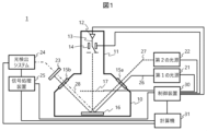
- Fig. 1 shows a schematic configuration of the inspection apparatus 1 of the first embodiment.
- the inspection apparatus 1 has, as main components, a charged particle beam device for controlling the electronic state of the sample to be inspected in the sample, a light irradiation system for irradiating the sample with probe light, and It has a photodetection system for detecting signal light and a control system for controlling them.
- the charged particle beam device includes a sample chamber 10 and a lens barrel 11, the insides of which are kept in a vacuum atmosphere by an exhaust mechanism (not shown).
- a sample chamber 10 accommodates a sample 16 such as a semiconductor wafer.
- a charged particle source 12 for generating a charged particle beam 13 to irradiate a sample 16 and a blanker 14 for chopping the charged particle source 12 are accommodated in the lens barrel 11 .
- the charged particle source 12 it is sufficient to generate the charged particle beam 13 for charging the sample 16, and an electron gun, a flood gun, an ion source, or the like can be used.
- charged particle optical components such as lenses and deflectors that form a charged particle optical system for guiding the charged particle beam 13 to the sample 16 may be provided.
- a charge control electrode 17 is provided near the sample 16 to control the charge amount of the sample 16 by controlling the electric field on the sample 16 .
- the electric field directly above the sample 16 is controlled by applying a voltage to the charge control electrode 17 .
- the electric field applied to the charge control electrode 17 causes secondary charged particles generated when the charged particle beam 13 is applied to the sample 16 to move away from or push back from the sample 16, thereby controlling the charged state of the sample 16.
- the charge control electrode 17 is arranged at a position separated from the sample 16 by several to 30 mm, for example. For this reason, it is desirable to use a metal mesh or a perforated electrode plate so as not to interfere with irradiation of the charged particle beam 13 or probe light 26 or pump light 27 (to be described later) onto the sample 16 .
- the charge of the sample 16 can be quickly removed by using ultraviolet light as disclosed in Patent Document 1.
- ultraviolet light As disclosed in Patent Document 1.
- a second light source 22 is provided to irradiate the sample 16 with light (referred to as pump light (second light) 27).
- pump light second light
- the electronic state of the sample to be inspected can be controlled, and by selecting the wavelength of the pump light 27, the content of the electronic state to be controlled can be changed.
- the second light source 22 can be configured in the same manner as the first light source 21 described later.
- the inspection apparatus 1 includes a first light source 21 that irradiates the sample 16 with probe light (first light) 26 in order to optically inspect a film to be inspected formed on the sample 16 .
- a white light source such as a xenon lamp, a laser, an LED, or the like can be used.
- a white light source can also be used after being monochromatized through a monochromator.
- the light irradiation system includes optical components such as lenses and mirrors constituting an optical system for guiding the probe light 26 to the sample 16 and a polarizer for controlling the polarization of the probe light 26. ing.
- the first light source 21 is arranged outside the sample chamber 10, and the probe light 26 is introduced into the sample chamber 10 through the view port 15a provided in the sample chamber 10.
- the pump light 27 is also introduced into the sample chamber 10 through the viewport 15a, but the probe light 26 and the pump light 27 may be introduced into the sample chamber 10 through different viewports.
- Signal light 28 is generated by irradiating the sample 16 with the probe light 26 .
- the signal light 28 includes reflected light, scattered light (including Raman scattered light), emitted light, and diffracted light.
- the photodetection system detects signal light 28 and includes an optical filter 23 , a photodetection system 24 and a signal processor 25 .
- the optical filter 23 is a filter that removes light other than the signal light 28
- the light detection system 24 detects the signal light 28 by receiving the light transmitted through the viewport 15 b through the optical filter 23 .
- a power meter, photodiode, spectrometer, or the like can be used according to the signal light 28 to be detected.
- the signal processor 25 processes the detection signals of the photodetection system obtained under the electric field conditions inside a plurality of samples.
- the signal processor 25 is, for example, a lock-in amplifier, and extracts the modulation intensity, phase, etc. of the detection signal from the photodetection system 24 .
- the signal light 28 detected by the photodetection system 24 is determined according to the film quality of the film to be inspected. For example, information such as interfacial electric field, defects, and strain can be obtained by detecting reflected light, information such as vibration level, stress, and strain can be obtained by detecting scattered light (including Raman scattered light), and luminescence can be detected. By detecting the diffracted light, information such as structural periodicity and refractive index can be obtained.
- the control device 30 controls components of the inspection device 1 .
- the control device 30 controls the operation of the charged particle beam device, the light irradiation system, and the light detection system, for example, based on inspection conditions input from the computer 31 .
- the control device 30 is implemented by a program executed by a processor such as a CPU. Alternatively, for example, it may be configured by FPGA (Field-Programmable Gate Array), ASIC (Application Specific Integrated Circuit), or the like.
- the computer 31 executes the inspection by the inspection device 1, the setting of measurement conditions, and the estimation of the film quality based on the detection signal from the photodetection system.
- the calculator 31 stores various databases or conversion formulas necessary for setting conditions and estimating film quality.
- the setting of inspection and measurement conditions includes the setting of the following parameters. These parameters are set by the user through the GUI of the computer 31 .
- the conditions of the charged particle beam 13 that charges the sample include acceleration voltage, current amount, irradiation area, irradiation position, and irradiation cycle by a blanker.
- the conditions of the charge control electrode 17 for controlling the charge amount of the sample include the voltage value and its application period.
- the conditions of the pump light 27 that control static electricity removal or the internal electric field of the sample include wavelength, intensity, polarization, irradiation period, and the like.
- Conditions of the probe light 26 include wavelength, intensity, polarization, and the like.
- Detector conditions of the photodetection system 24 include gain and the like.
- Figures 2A to 2C show an example of a control sequence that modulates the electronic state of the sample. Both examples are control sequences for controlling the electronic state of the sample 16 by three action sources, the charged particle beam 13 , the charge control electrode 17 and the pump light 27 .
- the conditions of the charged particle beam 13 and charge control electrode 17 are fixed, and the conditions of the pump light 27 are modulated.
- the parameter to be modulated may be wavelength or polarization, but intensity is used here.
- the intensity of the pump light 27 is ON, the charge of the sample 16 is removed or the electric field inside the sample is controlled depending on the wavelength of the pump light 27 .
- FIG. 2B the conditions of the charged particle beam 13 and the pump light 27 are fixed, and the conditions of the charge control electrode 17 are modulated.
- FIG. 2C fixes the conditions of the charge control electrode 17 and the pump light 27 and modulates the conditions of the charged particle beam 13 .
- Any parameter of at least one of the three action sources may be modulated so that the electronic state of the sample 16 is modulated.
- the modulation patterns of the multiple sources may be the same or different.
- the pump light 27 has a short wavelength and is used for the purpose of neutralizing the film to be inspected, and if it is sufficient to control only the presence or absence of the charge on the sample, the charge control electrode 17 can be eliminated.
- the second light source 22 when the charged particle beam 13 and charge control electrode 17 modulate the charge amount of the sample, the second light source 22 can be omitted.
- the second light source 22 capable of irradiating light with a wavelength longer than that of the ultraviolet light, and the If it is desired to reset the charge amount, it is effective to provide the second light source 22 capable of irradiating ultraviolet light.
- the detection signal output by the photodetection system after detecting the signal light 28 is sampled according to a sampling trigger.
- the sampling trigger is synchronized with the modulation of the electronic state of the sample.
- the intensity S A of the signal light 28 when the source to be modulated is in the first state the intensity of the pump light 27 is OFF in the example of FIG. 2A
- the source to be modulated is in the second state
- the intensity S B of the signal light 28 can be obtained when the intensity of the pump light 27 is ON
- information about the film quality of the film to be inspected can be obtained.
- the sampling trigger has various aspects depending on the configuration of the photodetection system, and is not limited to any particular aspect.
- the second light source 22 modulates the pump light 27 in synchronization with the synchronization signal from the control device 30 and the photodetection system continuously outputs detection signals from the signal processing device 25 .
- the computer 31 can receive the synchronization signal from the control device 30 and sample the detection signal from the signal processing device 25 with a sampling trigger synchronized with the synchronization signal.
- the photodetection system 24 continuously outputs a detection signal
- the signal processing device 25 receives a synchronization signal from the control device 30, and the detection from the photodetection system 24 is performed by a sampling trigger synchronized with the synchronization signal. It may be configured to sample a signal and perform signal processing. Further, in the photodetection system, the photodetection system 24 may receive a synchronizing signal from the control device 30 and may detect the signal light 28 by a sampling trigger synchronized with the synchronizing signal. This configuration is preferred when the detector of photodetection system 24 is a spectrometer.
- Signal processing of the signal processing device 25 in the photodetection system will be described.
- the detector in the photodetection system 24 is a power meter and the signal light 28 is the reflected light of the probe light 26 .
- the signal intensity S A of the signal light 28 in the first state and the signal intensity S B of the signal light 28 in the second state are assumed.
- the signal processing device 25 normalizes the difference between the signal intensities obtained in the two electronic states and outputs it as a detection signal.
- the detection signal is expressed as (Equation 1), which means the rate of change in reflectance.
- FIG. 3A shows the case where the voltage of the charge control electrode 17 is set to 0V
- FIG. 3B shows the case where the voltage of the charge control electrode 17 is set to +3V.
- the calculator 31 estimates the film quality, for example, the strain and dopant concentration of the semiconductor at the interface between the insulating film and the semiconductor, from the intensity and shape of the detected signal spectrum as shown in FIG. 3A or 3B.
- the obtained detection signal spectrum has, for example, a relationship represented by (Equation 3) (Non-Patent Document 1).
- A is intensity
- ⁇ is phase
- E energy
- ECP critical point energy
- ⁇ broadening factor
- n is a coefficient dependent on the material of the film to be inspected.
- (Formula 3) is fitted to the obtained detection signal spectrum. Fitting parameters (A, ⁇ , E CP , ⁇ ) included in (Equation 3) are obtained by fitting.
- the computer 31 holds film quality information for various combinations of fit parameters as a database.
- FIG. 4 shows an example of the database.
- FIG. 4 is an example data structure of the database 41 for estimating the film quality.
- film strain amounts (Strain) for combinations of fit parameters (A, ⁇ , E CP , ⁇ ) are registered.
- the computer 31 compares the fit parameter obtained from (Equation 3) with the database 41 to estimate the strain amount of the film to be inspected.
- the database 41 may register the film quality information as a function with the fit parameter as an argument, and the registration form is not limited.
- This example is an example in which a model formula such as Equation 3 and a database 41 are used when strain measurement is performed using the signal light 28 as the reflected light of the probe light 26.
- the signal light 28 is scattered light
- a model formula or database corresponding to the object may be used.
- the computer 31 stores the relationship between the parameters obtained from the detection signal and the film quality as a database, and estimates the film quality information from the parameters detected from the signal light 28 .
- the computer 31 has a database corresponding to the detection signal from the photodetection system and the analytical expression used in the film quality inspection performed by the inspection apparatus 1, and uses the database corresponding to the inspection to be performed to estimate the film quality.
- FIG. 5 shows a control flow for film quality inspection that can be estimated from the electric field dependence of such detection signals.
- a case of estimating the movable charge amount of a film to be inspected by applying the control sequence of FIG. 2A will be described as an example.
- variable parameter is the voltage applied to the charge control electrode 17 .
- a control sequence for film quality measurement is set. As described above, the control sequence of FIG. 2A is set (S02). After executing the control sequence and measuring the signal light 28 while changing the variable parameter (S03 to S06), and obtaining the detection signal for the range of the set variable parameter, a feature quantity indicating the dependence of the detection signal on the variable parameter is obtained. is calculated (S07).
- the computer 31 has a database of film quality information with respect to feature amounts that indicate variable parameter dependency of detection signals. This database is referenced to estimate the film quality of the film to be inspected (S08).
- FIG. 6 shows changes in intensity of the detection signal ( ⁇ R/R) when the voltage applied to the charge control electrode 17 is swept in the forward direction (from negative to positive) and the reverse direction (from positive to negative).
- the horizontal axis is the surface potential V s of the sample 16 . Since the surface potential Vs has a relationship with the applied voltage Vcc of the charge control electrode 17 as shown in (Equation 4), it can be obtained by converting from the applied voltage Vcc . (Formula 4) is obtained by simulation or the like.
- FIG. 7 is an example data structure of the database 51 for estimating the film quality obtained from the electric field dependence of the detection signal.
- the movable charge amount of the film is registered with respect to the combination of the feature amounts (V1, V2, ⁇ V) that indicate the electric field intensity dependence of the detection signal.
- the computer 31 compares the feature values (here, voltages V1, V2 and hysteresis that provide a specific reflectance) representing the electric field intensity dependence obtained from the measurement results as shown in FIG. Estimate the amount of mobile charge in the target membrane.
- the database 51 may register the film quality information as a function with the feature amount as an argument, and the registration form is not limited.
- FIG. 8 shows a display example of the result of optical inspection by the inspection device 1.
- Optical inspection is performed, for example, on user-designated chip sections on a semiconductor wafer.
- Optical inspection may be performed on the entire chip section.
- the film quality for each chip section subjected to optical inspection is displayed as a wafer heat map 60 .
- chip sections 62 are displayed in the wafer 61. For example, if the inspected film quality is defective, a chip section with a higher defect density is displayed in a darker color. This allows the user to visually recognize the film quality for each chip section.
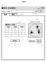
- FIG. 9A shows an example of a setting/measurement screen 70, which is a GUI (Graphical User Interface) for measuring film quality with the inspection device 1 and displaying the results.
- the setting/measurement screen 70 is provided with a setting file selection section 71, which can call the setting file saved in the computer 31 in the past measurement. For example, when inspecting different film qualities for the same wafer, the user's workload can be reduced by utilizing the past settings.
- control sequence tab 72 By selecting the control sequence tab included in the setting tab 72, the control sequences of FIGS. 2A to 2C or other control sequences can be selected.
- the laser modulation tab 73 is selected, and in this case, as shown in the sequence diagram 74, the control sequence for modulating the pump light shown as FIG. 2A is selected.
- an electron beam is used as the charged particle beam
- a laser beam is used as the pump light.
- the user opens the laser modulation tab 73 and sets the conditions for modulating the electronic state of the wafer in the electron beam condition setting section 75, charge control electrode condition setting section 76, and laser condition setting section 77. Furthermore, in this example, in order to estimate the film quality from the electric field dependence of the detection signal, the charge control electrode condition setting unit 76 is set to sweep the applied voltage. In this case, a sweep range setting section 78 is displayed, and the user sets the range for sweeping the applied voltage. When the above settings are completed, the save button 79 is pressed to save the set contents.
- the user After completing the condition setting, the user opens the measurement tab 81 as shown in FIG. 9B.
- the user designates a chip section for optical inspection in the inspection chip section setting section 82 and presses an inspection execution button 83 .
- optical inspection is performed on the designated chip section under the conditions set in the setting tab 72 .
- a wafer heat map is displayed on the wafer heat map display section 84 to simply show the inspection results to the user.
- the user confirms the inspection result and presses the save button 85 to save the optical inspection result.
- a result data file to be displayed in detail is called from a result file selection section 91 provided on the result output screen 90 .
- a wafer heat map display section 92 and a histogram display section 93 that display the same wafer heat map as the setting/measurement screen 70 are provided.
- the histogram displayed on the histogram display section 93 indicates the appearance frequency (the number of chip sections) of shades indicating the defect density in the wafer heat map displayed on the wafer heat map display section 92 .
- the inspection chip section measurement result display section 94 displays the measurement result of the detection signal in a specific chip section and the estimated film quality information.
- FIG. 10A shows a modification of the inspection apparatus 1 shown in FIG.
- the sample surface potential Vs is converted from the voltage Vcc applied to the charge control electrode 17 using (Equation 4). ) is obtained by simulations, etc.
- an error may occur between the value obtained from (Formula 4) and the true sample surface potential Vs.
- the inspection apparatus 1b of FIG. 10A has an energy filter 101 and a signal electron detector 102 as a mechanism for actually measuring the sample surface potential Vs of the sample 16.
- the signal electron detector 102 is a detector for detecting signal electrons 100 generated by irradiation of the sample 16 with the charged particle beam 13, and the signal electrons 100 to be detected are secondary electrons. may be reflected electrons (backscattered electrons).
- a negative voltage is applied to the energy filter 101 by the controller 30 , and only signal electrons that can overcome the electric field barrier caused by the negative voltage are detected by the signal electron detector 102 . That is, the amount of signal electrons detected by the signal electron detector 102 depends on the voltage of the energy filter 101 .
- the computer 31 of the inspection apparatus 1b calculates the sample surface potential Vs from the energy of the signal electrons 100.
- FIG. 10B shows the relationship between the amount of detected signal electrons and the energy filter voltage.
- a signal electron spectrum can be acquired by detecting the signal electron detection amount while changing the negative voltage applied to the energy filter 101 .
- the amount of shift depends on the sample surface potential Vs. This is because the force for pulling back the signal electrons 100 toward the sample changes depending on the sample surface potential Vs. If the signal electron spectrum 103 is the signal electron spectrum when the sample 16 is uncharged, the signal electron spectra 104 and 105 are the signal electron spectra when the sample 16 is positively charged and negatively charged, respectively.
- the sample surface potential Vs is defined as the voltage at which the differential value of the signal electron spectrum is maximum
- the potentials in the uncharged, positively charged, and negatively charged states are potentials V 0 , V 1 , and V 2 , respectively.
- the sample surface potential Vs can be actually measured without using the conversion formula (Equation 4).
- the signal electron spectrum 103 can be obtained by measuring the sample 16 in a state in which the charge is removed by the short wavelength pump light 27 such as ultraviolet light.
- the energy of the signal electrons 100 is discriminated using the energy filter 101, but the sample surface potential V It is possible to measure s .
- FIG. 11 shows a modification of the inspection apparatus 1 shown in FIG. Similar to Modification 1, Modification 2 also makes it possible to actually measure the sample surface potential Vs.
- the inspection apparatus 1 c has a surface potential meter 110 as a mechanism for actually measuring the sample surface potential Vs of the sample 16 .
- the sample 16 is moved to the position of the surface potential meter 110 provided in the sample chamber 10, and the sample surface potential Vs is measured.
- Example 1 the sample 16 is placed in a vacuum atmosphere, and it takes time to evacuate, which reduces the throughput of inspection measurement.
- Example 2 is a configuration example in which the sample 16 is placed in the air.
- the charged particle source 12 is arranged inside a lens barrel 11 that is in a vacuum atmosphere, and the lens barrel 11 is provided with a partition wall 120 for keeping the inside in a vacuum atmosphere.
- the charged particle beam 13 emitted from the charged particle source 12 passes through the partition wall 120 and is emitted to the atmosphere, and the sample 16 is irradiated with the beam.
- the charged particle source 12 is an electrode that generates ions by corona discharge in the atmosphere, the column 11 and the partition wall 120 for keeping the charged particle source in a vacuum atmosphere can be eliminated.
- Example 3 photoelectrons generated by irradiating a metal electrode with excitation light are used as charged particles.
- the inspection apparatus 3 of the third embodiment uses an electron beam source with a simple configuration as a charged particle beam source, and detects photoelectrons generated by irradiating the sample 16 and/or the charge control electrode 17 with short-wavelength light.
- the exchange can modulate the charge amount of the sample 16 .
- the third light source 131 and the fourth light source 132 are light sources that generate light with a wavelength of less than 400 nm, and their outputs are controlled by the control device 30 .
- the third light source 131 and the fourth light source 132 can be configured similarly to the first light source 21, respectively.
- a third light source 131 and a fourth light source 132 are arranged outside the sample chamber 10, and light from these light sources is introduced into the sample chamber 10 through a viewport 15c provided in the sample chamber 10. .
- the charge control electrode 17 is irradiated with the first excitation light (third light) 133 from the third light source 131 .
- a first photoelectron 135 is generated from a place irradiated with the first excitation light 133 . If the potential of the charge control electrode 17 is more negative than that of the sample 16 , the first photoelectrons 135 receive a force toward the sample and irradiate the sample 16 . Therefore, the sample 16 is negatively charged.
- the sample 16 is irradiated with the second excitation light (fourth light) 134 from the fourth light source 132 .
- a second photoelectron 136 is generated from a place irradiated with the second excitation light 134 . If the potential of the charge control electrode 17 is more positive than that of the sample 16 , the second photoelectrons 136 receive a force toward the charge control electrode and move away from the sample 16 . Therefore, the sample 16 is positively charged.
- the potential of the sample 16 can be modulated and controlled by the first photoelectrons 135 and the second photoelectrons 136 caused by the first excitation light 133 and the second excitation light 134 .
- the third light source 131 and the fourth light source 132 can also be used as one light source. Control.
- the configuration may be such that both the charge control electrode 17 and the sample 16 are irradiated with the excitation light at the same time.
- the third light source and the fourth light source may be arranged in a vacuum in order to avoid absorption of short wavelength light in the atmosphere.
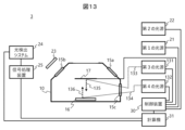
- the arrangement of the charge control electrode 17 and the charged particle source 12 interferes with the probe light (first light) 26 and the pump light (second light) 27, and the light irradiation system , the photodetection system cannot be placed near the sample 16 . Therefore, it is difficult to focus the light on the sample, and the spatial resolution of the measurement is limited.
- an optical system such as an objective lens for probe light and signal light is arranged directly above the sample in order to obtain a high spatial resolution.
- an optical lens 141 for irradiating the sample 16 with the probe light 26 and the pump light 27 is positioned directly above the sample, and the optical axis thereof extends in a direction perpendicular to the film to be inspected formed on the sample. is located in Since the probe light 26 and the pump light 27 are focused on the sample 16 by the optical lens 141, measurement with high spatial resolution is possible.
- the charged particle source 12 is obliquely arranged with respect to the optical axis of the optical lens 141 , and the charged particle beam 13 passes between the optical lens 141 and the sample 16 and obliquely irradiates the sample 16 .
- the optical lens 141 also functions as a charge control electrode. That is, a transparent conductive film 17b is formed on the optical lens 141, and a voltage can be applied by the controller 30 while allowing the probe light 26, the pump light 27, and the signal light 28 to pass therethrough.
- a transparent conductive film 17b ITO, ITZO or the like may be used, or a metal thin film such as aluminum or gold may be used.
- the charge control electrode may be a transparent electrode and arranged under the optical lens 141 separately from the optical lens 141 .
- the probe light 26 and the pump light 27 are integrated on the same optical path using a dichroic mirror 142 having different transmission/reflection characteristics depending on the wavelength of the light.
- Signal light 28 propagates back through the optical path of probe light 26 , is reflected by beam splitter 143 , passes through optical filter 23 and is detected by photodetection system 24 .
- the probe light 26 is focused on the sample 16 by the optical lens 141, so that film quality measurement can be performed with high spatial resolution.
- the optical lens 141 is arranged in the vicinity of the sample 16, there is also the advantage that the detection rate for scattered light and emitted light from the sample 16 is improved.
- FIG. 14 illustrates only representative optical components that constitute the optical system, and omits general elements such as lenses and mirrors.
Abstract
In the present invention, film qualities of deposited semiconductor film, insulating film, and the like are inspected in a non-contact manner. This inspection device (1) for inspecting the film quality of a film formed on a sample (16) has: a charged particle source (12) for irradiating the sample with a charged particle beam (13); a first light source (21) for irradiating the sample with first light (26); a photodetection system for detecting signal light (28) generated when the sample is irradiated with the first light; a charge control electrode (17) for controlling an electric field on the sample, or a second light source (22) for irradiating the sample with second light (27); a control device (30) for modulating the sample's electronic state by using the charged particle source as well as the charge control electrode or the second light source; and a computer (31) for estimating the film quality of the film formed on the sample on the basis of a detection signal of signal light which has been modulated in accordance with the sample's modulated electronic state, the detection signal being output from the photodetection system.
Description
本開示は、検査装置およびそれを用いた膜質検査方法に関する。
The present disclosure relates to an inspection device and a film quality inspection method using the same.
特許文献1には、除電用の紫外光を搭載したSEMが記載されている。絶縁膜の帯電は紫外光の照射によって除去できることが知られている。特許文献2には、試料上の電界を制御する帯電制御電極が搭載されたSEMが記載されている。帯電制御電極の電圧を制御することによって電子線照射により帯電する試料の帯電量を制御できることが知られている。
Patent Document 1 describes an SEM equipped with ultraviolet light for static elimination. It is known that electrification of an insulating film can be removed by irradiation with ultraviolet light. Patent Literature 2 describes an SEM equipped with charge control electrodes that control the electric field on the sample. It is known that the charge amount of a sample charged by electron beam irradiation can be controlled by controlling the voltage of the charge control electrode.
半導体デバイスにおいて、その半導体膜や絶縁膜の膜質は重要である。例えば、トランジスタの性能は、ゲート絶縁膜の性質やゲート絶縁膜とその接する層との界面の性質などによって大きく左右される。絶縁膜や界面に欠陥が存在すると、デバイス駆動時の電界印加により欠陥に電荷が蓄積され、デバイス動作に悪影響を及ぼす。この欠陥のようにデバイス動作時に問題となるような膜質の検査には、デバイス動作時と同様に検査対象膜に電界を印加してその特性変化を測定することが有効である。
In semiconductor devices, the film quality of the semiconductor film and insulating film is important. For example, the performance of a transistor is greatly affected by the properties of the gate insulating film, the properties of the interface between the gate insulating film and its contacting layer, and the like. If defects exist in the insulating film or interface, electric charges are accumulated in the defects due to the application of an electric field during device driving, which adversely affects the device operation. In order to inspect film quality such as defects that may cause problems during device operation, it is effective to apply an electric field to the film to be inspected and measure changes in its characteristics in the same manner as during device operation.
デバイスを完成させた後においては、デバイスを実際に動作させる電気特性検査によって膜質は検査できる。しかしながら、完成後の検査では、量産工程における不具合の作り込みを未然に防ぐことができない。また、半導体製造プロセスの開発においては、検査対象膜を挟み込む電極を作製して電極間に電圧を印加することにより、電界印加下での膜質の測定が可能になるが、このための電極の作製には時間もコストもかかる。
After the device is completed, the film quality can be inspected by electrical property inspection in which the device is actually operated. However, the inspection after completion cannot prevent defects from being incorporated in the mass production process. In addition, in the development of semiconductor manufacturing processes, it is possible to measure the film quality under the application of an electric field by fabricating electrodes sandwiching the film to be inspected and applying a voltage between the electrodes. is time consuming and costly.
したがって、半導体デバイスの量産工程において、あるいは半導体製造プロセス開発において、成膜した半導体膜や絶縁膜などの膜質を非接触で検査することが望まれる。ここで、膜質とは、成膜された材料が含む電荷、歪、欠陥、あるいは下地の状態、界面の状態等によって当該膜が示す材料特性をいう。また、本発明において検査対象とする膜としては半導体デバイスの製造工程において形成される膜を広く含むものとし、膜の製法や材料を問わない。例えば、成膜後にアニール等の加工を行った膜、半導体基板を熱酸化して得られる膜(熱酸化膜)、半導体基板にイオン注入により形成される膜なども対象となる。また、材料も無機材料、有機材料ともに含まれる。
Therefore, in the mass production process of semiconductor devices or in the development of semiconductor manufacturing processes, it is desired to inspect the film quality of deposited semiconductor films and insulating films without contact. The term "film quality" as used herein refers to the material characteristics of a film due to charges, distortions, defects, or the state of the underlying layer, the state of the interface, or the like contained in the material formed into the film. In the present invention, the film to be inspected includes a wide range of films formed in the manufacturing process of semiconductor devices, regardless of the manufacturing method or material of the film. For example, films processed such as annealing after deposition, films obtained by thermally oxidizing a semiconductor substrate (thermal oxide film), and films formed by ion implantation in a semiconductor substrate are also included. Materials are also included in both inorganic materials and organic materials.
本発明の一態様である検査装置は、試料上に形成された膜の膜質を検査する検査装置であって、試料に荷電粒子線を照射する荷電粒子源と、試料に第1の光を照射する第1の光源と、第1の光が試料に照射されることにより発生する信号光を検出する光検出系と、試料上の電界を制御する帯電制御電極または試料に第2の光を照射する第2の光源と、荷電粒子源と、帯電制御電極または第2の光源とを用いて、試料の電子状態を変調させる制御装置と、光検出系から出力される試料の電子状態の変調に応じて変調された信号光の検出信号に基づき試料上に形成された膜の膜質を推定する計算機を有する。
An inspection apparatus according to one aspect of the present invention is an inspection apparatus for inspecting the film quality of a film formed on a sample, comprising a charged particle source for irradiating the sample with a charged particle beam, and a first light for irradiating the sample. a light detection system for detecting signal light generated by irradiating the sample with the first light; and a charge control electrode for controlling the electric field on the sample or irradiating the sample with the second light. A control device for modulating the electronic state of the sample using a second light source, a charged particle source, a charge control electrode or the second light source, and a control device for modulating the electronic state of the sample output from the photodetection system. It has a computer for estimating the film quality of the film formed on the sample based on the detection signal of the signal light modulated accordingly.
本発明の一態様である膜質検査方法は、試料上に形成された膜の膜質を検査する膜質検査方法であって、試料に荷電粒子線を照射して、試料を帯電させ、試料の電子状態を変調させた状態で試料にプローブ光を照射し、プローブ光が試料に照射されることにより発生する信号光を検出し、試料の電子状態の変調に応じて変調された信号光の検出信号に基づき、試料上に形成された膜の膜質を推定する。
A film quality inspection method, which is one aspect of the present invention, is a film quality inspection method for inspecting the film quality of a film formed on a sample, wherein the sample is irradiated with a charged particle beam to charge the sample, thereby determining the electronic state of the sample. is modulated, the sample is irradiated with probe light, the signal light generated by the irradiation of the probe light onto the sample is detected, and the detection signal of the signal light modulated according to the modulation of the electronic state of the sample is Based on this, the film quality of the film formed on the sample is estimated.
成膜した半導体や絶縁膜などの膜質を非接触で検査することが可能になる。その他の課題と新規な特徴は、本明細書の記述および添付図面から明らかになるであろう。
It will be possible to inspect the film quality of deposited semiconductors and insulating films without contact. Other problems and novel features will become apparent from the description of the specification and the accompanying drawings.
以下、本発明の実施例について説明する。なお、本実施例で示す図面は本発明の具体的例を示しているが、これらは本発明の理解のためのものであり、決して本発明を限定的に解釈するために用いられるものではない。
Examples of the present invention will be described below. Although the drawings shown in the present embodiment show specific examples of the present invention, they are for the purpose of understanding the present invention and are not used to interpret the present invention in a limited way. .
本実施例の検査装置では、膜質を光学検査によって評価する。すなわち、具体例は後述するが、膜が有する材料特性を膜の光学特性として検出し、検出された光学特性から膜質についての情報を得る。本実施例では、光学検査にあたり、検査対象膜の帯電制御及び/または光照射による内部電界制御により、検査対象試料の電子状態を変調制御する。
The inspection apparatus of this embodiment evaluates film quality by optical inspection. That is, although a specific example will be described later, the material characteristics of the film are detected as the optical characteristics of the film, and information about the film quality is obtained from the detected optical characteristics. In this embodiment, in the optical inspection, the electronic state of the sample to be inspected is modulated and controlled by charge control of the film to be inspected and/or internal electric field control by light irradiation.
以下の実施例において、検査対象膜上の電界強度を制御する目的は大きく2つに分けられる。第一は、光学検査の条件を最適化することである。例えば、最大の信号光強度を得られる電界強度下で光学検査を行うことで、高SNRでの検査を行うことができ、検査のスループットを向上させることができる。第二は、電界依存する膜質を検査することである。電界強度に依存する材料特性は、印加する電界強度を変えて検出信号の変化を検出することで、膜質についての情報を得ることができる。詳細については後述する。
In the following examples, the purpose of controlling the electric field strength on the film to be inspected can be roughly divided into two. The first is to optimize the conditions of optical inspection. For example, by performing an optical inspection under an electric field strength that can obtain the maximum signal light intensity, it is possible to perform an inspection with a high SNR, and improve the inspection throughput. The second is to examine field-dependent film quality. Information on the film quality can be obtained by changing the applied electric field strength and detecting changes in the detection signal for the material properties that depend on the electric field strength. Details will be described later.
以下では、検査対象を半導体ウェハの上に成膜された絶縁膜とその界面として実施例を開示するが、本技術の適用先はこれに限られない。電界下での膜質測定は、例えば半導体膜や有機膜、それらの界面でも有効である。
In the following, an embodiment will be disclosed in which the object to be inspected is an insulating film formed on a semiconductor wafer and its interface, but the application of this technology is not limited to this. Film quality measurement under an electric field is also effective for, for example, semiconductor films, organic films, and their interfaces.
図1に実施例1の検査装置1の概略構成を示す。検査装置1は、主要な構成として、試料における検査対象試料の電子状態を制御する荷電粒子線装置、試料にプローブ光を照射する光照射系、試料にプローブ光が照射させることに起因して生じる信号光を検出する光検出系、これらを制御する制御系を有する。
Fig. 1 shows a schematic configuration of the inspection apparatus 1 of the first embodiment. The inspection apparatus 1 has, as main components, a charged particle beam device for controlling the electronic state of the sample to be inspected in the sample, a light irradiation system for irradiating the sample with probe light, and It has a photodetection system for detecting signal light and a control system for controlling them.
(荷電粒子線装置)
荷電粒子線装置は、試料室10と鏡筒11とを備え、これらの内部は図示しない排気機構により真空雰囲気に保持される。試料室10には、半導体ウェハのような試料16が収容される。鏡筒11には、試料16に照射する荷電粒子線13を発生させる荷電粒子源12、荷電粒子源12をチョッピングするブランカ14が収容されている。ここで、荷電粒子源12としては、試料16を帯電させるための荷電粒子線13を発生できればよく、電子銃、フラッドガン、イオン源などが使用できる。また、荷電粒子線13を試料16に導くための荷電粒子光学系を構成するレンズや偏向器などの荷電粒子光学部品を備えていてもよい。 (charged particle beam device)
The charged particle beam device includes asample chamber 10 and a lens barrel 11, the insides of which are kept in a vacuum atmosphere by an exhaust mechanism (not shown). A sample chamber 10 accommodates a sample 16 such as a semiconductor wafer. A charged particle source 12 for generating a charged particle beam 13 to irradiate a sample 16 and a blanker 14 for chopping the charged particle source 12 are accommodated in the lens barrel 11 . Here, as the charged particle source 12, it is sufficient to generate the charged particle beam 13 for charging the sample 16, and an electron gun, a flood gun, an ion source, or the like can be used. Moreover, charged particle optical components such as lenses and deflectors that form a charged particle optical system for guiding the charged particle beam 13 to the sample 16 may be provided.
荷電粒子線装置は、試料室10と鏡筒11とを備え、これらの内部は図示しない排気機構により真空雰囲気に保持される。試料室10には、半導体ウェハのような試料16が収容される。鏡筒11には、試料16に照射する荷電粒子線13を発生させる荷電粒子源12、荷電粒子源12をチョッピングするブランカ14が収容されている。ここで、荷電粒子源12としては、試料16を帯電させるための荷電粒子線13を発生できればよく、電子銃、フラッドガン、イオン源などが使用できる。また、荷電粒子線13を試料16に導くための荷電粒子光学系を構成するレンズや偏向器などの荷電粒子光学部品を備えていてもよい。 (charged particle beam device)
The charged particle beam device includes a
試料16の近傍には、試料16上の電界を制御することで、試料16の帯電量を制御する帯電制御電極17が設けられている。帯電制御電極17に電圧を印加することで試料16直上の電界を制御する。帯電制御電極17に印加された電界が荷電粒子線13を試料16に照射した際に発生する二次荷電粒子を試料16から遠ざけるまたは押し戻すことで試料16の帯電状態が制御される。帯電制御電極17は、試料16から、例えば数~30mm程度離れた位置に配置される。このため、荷電粒子線13、あるいは後述するプローブ光26やポンプ光27を試料16に照射する障害にならないよう、金属メッシュや穴の開いた電極板によって構成することが望ましい。
A charge control electrode 17 is provided near the sample 16 to control the charge amount of the sample 16 by controlling the electric field on the sample 16 . The electric field directly above the sample 16 is controlled by applying a voltage to the charge control electrode 17 . The electric field applied to the charge control electrode 17 causes secondary charged particles generated when the charged particle beam 13 is applied to the sample 16 to move away from or push back from the sample 16, thereby controlling the charged state of the sample 16. FIG. The charge control electrode 17 is arranged at a position separated from the sample 16 by several to 30 mm, for example. For this reason, it is desirable to use a metal mesh or a perforated electrode plate so as not to interfere with irradiation of the charged particle beam 13 or probe light 26 or pump light 27 (to be described later) onto the sample 16 .
さらに、特許文献1に開示されているような紫外光を用いると素早く試料16の帯電を除去できる。一方、紫外光よりも長波長の光の場合、帯電状態は変化させることなく、試料内部の電界(界面電界)を制御できることが知られている。このため、図1の構成例では、試料16に光(ポンプ光(第2の光)27と呼ぶ)を照射する第2の光源22が設けられている。ポンプ光27を照射することで検査対象試料の電子状態を制御することができ、さらにポンプ光27の波長を選択することで、制御する電子状態の内容を変えることができる。具体的には、紫外光を用いることで試料帯電の除電及び界面電界の制御を行うことができ、紫外光よりも長波長の光を用いることで、界面電界の制御を行うことができる。第2の光源22は、後述する第1の光源21と同様に構成できる。
Furthermore, the charge of the sample 16 can be quickly removed by using ultraviolet light as disclosed in Patent Document 1. On the other hand, it is known that light with a wavelength longer than that of ultraviolet light can control the electric field (interfacial electric field) inside the sample without changing the charged state. Therefore, in the configuration example of FIG. 1, a second light source 22 is provided to irradiate the sample 16 with light (referred to as pump light (second light) 27). By irradiating the pump light 27, the electronic state of the sample to be inspected can be controlled, and by selecting the wavelength of the pump light 27, the content of the electronic state to be controlled can be changed. Specifically, by using ultraviolet light, it is possible to eliminate static charge on the sample and control the interfacial electric field, and by using light with a wavelength longer than that of the ultraviolet light, it is possible to control the interfacial electric field. The second light source 22 can be configured in the same manner as the first light source 21 described later.
(光照射系)
検査装置1は、試料16上に形成されている検査対象膜の光学検査を行うため、試料16にプローブ光(第1の光)26を照射する第1の光源21を備える。第1の光源21としては、キセノンランプなどの白色光源、レーザ、LEDなどを用いることができる。白色光源は、モノクロメータを通して単色化して使用することもできる。なお、図示していないが、光照射系は、プローブ光26を試料16に導くための光学系を構成するレンズやミラー、プローブ光26の偏光を制御するための偏光子などの光学部品を備えている。 (Light irradiation system)
Theinspection apparatus 1 includes a first light source 21 that irradiates the sample 16 with probe light (first light) 26 in order to optically inspect a film to be inspected formed on the sample 16 . As the first light source 21, a white light source such as a xenon lamp, a laser, an LED, or the like can be used. A white light source can also be used after being monochromatized through a monochromator. Although not shown, the light irradiation system includes optical components such as lenses and mirrors constituting an optical system for guiding the probe light 26 to the sample 16 and a polarizer for controlling the polarization of the probe light 26. ing.
検査装置1は、試料16上に形成されている検査対象膜の光学検査を行うため、試料16にプローブ光(第1の光)26を照射する第1の光源21を備える。第1の光源21としては、キセノンランプなどの白色光源、レーザ、LEDなどを用いることができる。白色光源は、モノクロメータを通して単色化して使用することもできる。なお、図示していないが、光照射系は、プローブ光26を試料16に導くための光学系を構成するレンズやミラー、プローブ光26の偏光を制御するための偏光子などの光学部品を備えている。 (Light irradiation system)
The
図1の例では、第1の光源21は試料室10の外側に配置され、プローブ光26は、試料室10に設けられたビューポート15aを介して試料室10内に導入されている。この例ではポンプ光27もビューポート15aを介して試料室10内に導入されているが、プローブ光26とポンプ光27とを異なるビューポートから試料室10に導入してもよい。
In the example of FIG. 1, the first light source 21 is arranged outside the sample chamber 10, and the probe light 26 is introduced into the sample chamber 10 through the view port 15a provided in the sample chamber 10. In this example, the pump light 27 is also introduced into the sample chamber 10 through the viewport 15a, but the probe light 26 and the pump light 27 may be introduced into the sample chamber 10 through different viewports.
(光検出系)
プローブ光26が試料16に照射させることにより、信号光28が発生する。信号光28としては、反射光、散乱光(ラマン散乱光を含む)、発光、回折光を含む。光検出系は信号光28を検出するものであり、光学フィルタ23、光検出システム24、信号処理装置25を備える。光学フィルタ23は信号光28以外の光を除去するフィルタであり、光検出システム24では、ビューポート15bを透過した光を、光学フィルタ23を介して受光することにより、信号光28を検出する。光検出システム24としては、検出する信号光28にあわせて、パワーメータ、フォトダイオード、スペクトロメータなどを用いることができる。信号処理装置25は、複数の試料内部の電界条件で得られた光検出システムの検出信号の処理を行う。信号処理装置25は例えば、ロックインアンプであり、光検出システム24からの検出信号の変調強度や位相等を抽出する。 (Photodetection system)
Signal light 28 is generated by irradiating thesample 16 with the probe light 26 . The signal light 28 includes reflected light, scattered light (including Raman scattered light), emitted light, and diffracted light. The photodetection system detects signal light 28 and includes an optical filter 23 , a photodetection system 24 and a signal processor 25 . The optical filter 23 is a filter that removes light other than the signal light 28 , and the light detection system 24 detects the signal light 28 by receiving the light transmitted through the viewport 15 b through the optical filter 23 . As the light detection system 24, a power meter, photodiode, spectrometer, or the like can be used according to the signal light 28 to be detected. The signal processor 25 processes the detection signals of the photodetection system obtained under the electric field conditions inside a plurality of samples. The signal processor 25 is, for example, a lock-in amplifier, and extracts the modulation intensity, phase, etc. of the detection signal from the photodetection system 24 .
プローブ光26が試料16に照射させることにより、信号光28が発生する。信号光28としては、反射光、散乱光(ラマン散乱光を含む)、発光、回折光を含む。光検出系は信号光28を検出するものであり、光学フィルタ23、光検出システム24、信号処理装置25を備える。光学フィルタ23は信号光28以外の光を除去するフィルタであり、光検出システム24では、ビューポート15bを透過した光を、光学フィルタ23を介して受光することにより、信号光28を検出する。光検出システム24としては、検出する信号光28にあわせて、パワーメータ、フォトダイオード、スペクトロメータなどを用いることができる。信号処理装置25は、複数の試料内部の電界条件で得られた光検出システムの検出信号の処理を行う。信号処理装置25は例えば、ロックインアンプであり、光検出システム24からの検出信号の変調強度や位相等を抽出する。 (Photodetection system)
Signal light 28 is generated by irradiating the
光検出システム24が検出する信号光28は、検査対象膜に対して検査を行う膜質に応じて定められる。例えば、反射光を検出することにより界面電界、欠陥、歪などの情報を、散乱光(ラマン散乱光を含む)を検出することにより振動準位、応力、歪みなどの情報を、発光を検出することにより欠陥、発光効率などの情報を、回折光を検出することにより構造周期性、屈折率などの情報を得ることができる。
The signal light 28 detected by the photodetection system 24 is determined according to the film quality of the film to be inspected. For example, information such as interfacial electric field, defects, and strain can be obtained by detecting reflected light, information such as vibration level, stress, and strain can be obtained by detecting scattered light (including Raman scattered light), and luminescence can be detected. By detecting the diffracted light, information such as structural periodicity and refractive index can be obtained.
(制御系)
制御装置30は、検査装置1の構成要素の制御を行う。制御装置30は、例えば、計算機31から入力される検査条件に基づき、荷電粒子線装置、光照射系、光検出系の動作制御を行う。制御装置30は、例えばCPU等のプロセッサで実行されるプロクラムにより実現される。また、例えば、FPGA(Field-Programmable Gate Array)やASIC(Application Specific Integrated Circuit)等で構成されてもよい。 (control system)
Thecontrol device 30 controls components of the inspection device 1 . The control device 30 controls the operation of the charged particle beam device, the light irradiation system, and the light detection system, for example, based on inspection conditions input from the computer 31 . The control device 30 is implemented by a program executed by a processor such as a CPU. Alternatively, for example, it may be configured by FPGA (Field-Programmable Gate Array), ASIC (Application Specific Integrated Circuit), or the like.
制御装置30は、検査装置1の構成要素の制御を行う。制御装置30は、例えば、計算機31から入力される検査条件に基づき、荷電粒子線装置、光照射系、光検出系の動作制御を行う。制御装置30は、例えばCPU等のプロセッサで実行されるプロクラムにより実現される。また、例えば、FPGA(Field-Programmable Gate Array)やASIC(Application Specific Integrated Circuit)等で構成されてもよい。 (control system)
The
検査装置1による検査、計測の条件設定や光検出系からの検出信号に基づく膜質の推定は計算機31によって実行される。計算機31は、条件設定や膜質の推定に必要な種々のデータベースまたは換算式を記憶している。
The computer 31 executes the inspection by the inspection device 1, the setting of measurement conditions, and the estimation of the film quality based on the detection signal from the photodetection system. The calculator 31 stores various databases or conversion formulas necessary for setting conditions and estimating film quality.
検査、計測の条件設定には、以下のようなパラメータの設定を含む。これらのパラメータは計算機31のGUIを通じて、ユーザが設定する。試料を帯電させる荷電粒子線13の条件には、加速電圧、電流量、照射面積、照射位置、ブランカによる照射周期などがある。試料の帯電量を制御する帯電制御電極17の条件には、電圧の値やその印加周期などがある。試料の除電あるいは内部電界を制御するポンプ光27の条件には波長、強度、偏光、照射周期などがある。プローブ光26の条件には波長、強度、偏光などがある。光検出システム24の検出器の条件にはゲインなどがある。
The setting of inspection and measurement conditions includes the setting of the following parameters. These parameters are set by the user through the GUI of the computer 31 . The conditions of the charged particle beam 13 that charges the sample include acceleration voltage, current amount, irradiation area, irradiation position, and irradiation cycle by a blanker. The conditions of the charge control electrode 17 for controlling the charge amount of the sample include the voltage value and its application period. The conditions of the pump light 27 that control static electricity removal or the internal electric field of the sample include wavelength, intensity, polarization, irradiation period, and the like. Conditions of the probe light 26 include wavelength, intensity, polarization, and the like. Detector conditions of the photodetection system 24 include gain and the like.
なお、制御装置30の機能を計算機31が実行するように構成することも可能である。
It should be noted that it is also possible to configure the computer 31 to execute the functions of the control device 30 .
図2A~Cに試料の電子状態を変調する制御シーケンスの例を示す。いずれの例も、試料16の電子状態を、荷電粒子線13、帯電制御電極17、ポンプ光27の3つの作用源により制御する制御シーケンスである。図2Aは、荷電粒子線13と帯電制御電極17の条件を固定し、ポンプ光27の条件を変調する。変調するパラメータは波長や偏光であってもよいが、ここでは強度としている。ポンプ光27の強度がON時には、ポンプ光27の波長に依存して試料16の帯電が除去され、あるいは試料内部の電界が制御される。図2Bは、荷電粒子線13とポンプ光27の条件を固定し、帯電制御電極17の条件を変調する。図2Cは、帯電制御電極17とポンプ光27の条件を固定し、荷電粒子線13の条件を変調する。試料16の電子状態が変調されるよう、3つの作用源の少なくとも1つ以上について、何らかのパラメータを変調させればよい。複数の作用源を変調させる場合には、複数の作用源の変調パターンは同じであっても、異なっていてもよい。また、ポンプ光27の波長を短波長として検査対象膜の除電を目的として使用し、試料の帯電の有無のみを制御できればよい場合には帯電制御電極17をなくすることも可能である。また、図2B,Cの制御シーケンスのように、荷電粒子線13と帯電制御電極17とにより試料の帯電量を変調する場合は第2の光源22をなくすことも可能である。ただし、そのような場合であっても、試料内部の電界(界面電界)を制御したい場合には、紫外光よりも長波長の光を照射可能な第2の光源22、さらに変調ごとに試料の帯電量をリセットしたい場合には、紫外光を照射可能な第2の光源22を設けておくことは有効である。
Figures 2A to 2C show an example of a control sequence that modulates the electronic state of the sample. Both examples are control sequences for controlling the electronic state of the sample 16 by three action sources, the charged particle beam 13 , the charge control electrode 17 and the pump light 27 . In FIG. 2A, the conditions of the charged particle beam 13 and charge control electrode 17 are fixed, and the conditions of the pump light 27 are modulated. The parameter to be modulated may be wavelength or polarization, but intensity is used here. When the intensity of the pump light 27 is ON, the charge of the sample 16 is removed or the electric field inside the sample is controlled depending on the wavelength of the pump light 27 . In FIG. 2B, the conditions of the charged particle beam 13 and the pump light 27 are fixed, and the conditions of the charge control electrode 17 are modulated. FIG. 2C fixes the conditions of the charge control electrode 17 and the pump light 27 and modulates the conditions of the charged particle beam 13 . Any parameter of at least one of the three action sources may be modulated so that the electronic state of the sample 16 is modulated. When multiple sources are modulated, the modulation patterns of the multiple sources may be the same or different. Also, if the pump light 27 has a short wavelength and is used for the purpose of neutralizing the film to be inspected, and if it is sufficient to control only the presence or absence of the charge on the sample, the charge control electrode 17 can be eliminated. 2B and 2C, when the charged particle beam 13 and charge control electrode 17 modulate the charge amount of the sample, the second light source 22 can be omitted. However, even in such a case, if it is desired to control the electric field (interfacial electric field) inside the sample, the second light source 22 capable of irradiating light with a wavelength longer than that of the ultraviolet light, and the If it is desired to reset the charge amount, it is effective to provide the second light source 22 capable of irradiating ultraviolet light.
光検出系が信号光28を検出して出力する検出信号のサンプリングはサンプリングトリガーにしたがって行われる。サンプリングトリガーは試料の電子状態の変調に同期している。これにより、変調される作用源が第1状態(図2Aの例ではポンプ光27の強度がOFF)のときの信号光28の強度SAと変調される作用源が第2状態(図2Aの例ではポンプ光27の強度がON)のときの信号光28の強度SBを得ることができ、強度SAと強度SBとを比較することにより、検査対象膜の膜質についての情報が得られる。図2A~Cの制御シーケンスはいずれも第1状態と第2状態との2種類の電子状態をつくるものであるが、複数の作用源を異なる変調パターンで変調させることにより、3種類以上の電子状態をつくるものであってもよい。
The detection signal output by the photodetection system after detecting the signal light 28 is sampled according to a sampling trigger. The sampling trigger is synchronized with the modulation of the electronic state of the sample. As a result, the intensity S A of the signal light 28 when the source to be modulated is in the first state (the intensity of the pump light 27 is OFF in the example of FIG. 2A) and the source to be modulated is in the second state ( In this example, the intensity S B of the signal light 28 can be obtained when the intensity of the pump light 27 is ON), and by comparing the intensity S A and the intensity S B , information about the film quality of the film to be inspected can be obtained. be done. All of the control sequences in FIGS. 2A to 2C create two types of electronic states, the first state and the second state. It may be something that creates a state.
ここでサンプリングトリガーには光検出系の構成に応じて様々な態様があり、特定の態様に限定されない。例えば、第2の光源22は制御装置30からの同期信号に同期してポンプ光27を変調させており、光検出系が信号処理装置25から連続的に検出信号を出力しているとする。この場合、計算機31は、制御装置30から同期信号を受信し、同期信号と同期するサンプリングトリガーにより信号処理装置25からの検出信号をサンプリングすることができる。または、光検出系において光検出システム24は連続的に検出信号を出力し、信号処理装置25が制御装置30から同期信号を受信し、同期信号と同期するサンプリングトリガーにより光検出システム24からの検出信号をサンプリングして信号処理を行うよう構成してもよい。さらに、光検出系において光検出システム24が制御装置30から同期信号を受信し、同期信号と同期するサンプリングトリガーにより信号光28を検出するよう構成してもよい。光検出システム24の検出器がスペクトロメータの場合は、この構成にするとよい。
Here, the sampling trigger has various aspects depending on the configuration of the photodetection system, and is not limited to any particular aspect. For example, it is assumed that the second light source 22 modulates the pump light 27 in synchronization with the synchronization signal from the control device 30 and the photodetection system continuously outputs detection signals from the signal processing device 25 . In this case, the computer 31 can receive the synchronization signal from the control device 30 and sample the detection signal from the signal processing device 25 with a sampling trigger synchronized with the synchronization signal. Alternatively, in the photodetection system, the photodetection system 24 continuously outputs a detection signal, the signal processing device 25 receives a synchronization signal from the control device 30, and the detection from the photodetection system 24 is performed by a sampling trigger synchronized with the synchronization signal. It may be configured to sample a signal and perform signal processing. Further, in the photodetection system, the photodetection system 24 may receive a synchronizing signal from the control device 30 and may detect the signal light 28 by a sampling trigger synchronized with the synchronizing signal. This configuration is preferred when the detector of photodetection system 24 is a spectrometer.
光検出系における信号処理装置25の信号処理について説明する。例えば、光検出システム24における検出器をパワーメータとし、信号光28をプローブ光26の反射光であるとする。図2Aの制御シーケンスを適用したとして、第1状態での信号光28の信号強度SA、第2状態での信号光28の信号強度SBとする。信号処理装置25は、2つの電子状態で取得した信号強度の差分を規格化して検出信号として出力する。この場合、検出信号は(数1)として表され、反射率の変化率を意味している。
Signal processing of the signal processing device 25 in the photodetection system will be described. For example, assume that the detector in the photodetection system 24 is a power meter and the signal light 28 is the reflected light of the probe light 26 . Assuming that the control sequence of FIG. 2A is applied, the signal intensity S A of the signal light 28 in the first state and the signal intensity S B of the signal light 28 in the second state are assumed. The signal processing device 25 normalizes the difference between the signal intensities obtained in the two electronic states and outputs it as a detection signal. In this case, the detection signal is expressed as (Equation 1), which means the rate of change in reflectance.
信号処理装置25としてロックインアンプを用いた場合には、振幅ΔR0、位相θが出力され、この場合、検出信号は(数2)として表される。
When a lock-in amplifier is used as the signal processing device 25, the amplitude ΔR 0 and the phase θ are output, and in this case the detection signal is expressed as (Equation 2).
プローブ光26の波長を変えながら検出信号ΔR/Rを検出すると図3Aまたは図3Bのようなスペクトルが得られる。横軸は反射光の波長またはエネルギーである。ここで、図3Aは帯電制御電極17の電圧を0Vに設定した場合であり、図3Bは帯電制御電極17の電圧を+3Vに設定した場合である。帯電制御電極17の電圧、すなわち試料16の帯電量を調整することにより、よりSNRの高い検出信号が得られている。なお、プローブ光26に白色光源と光検出システム24の検出器としてスペクトロメータを用いても同様のスペクトルを得ることが可能である。
When the detection signal ΔR/R is detected while changing the wavelength of the probe light 26, a spectrum as shown in FIG. 3A or 3B is obtained. The horizontal axis is the wavelength or energy of the reflected light. Here, FIG. 3A shows the case where the voltage of the charge control electrode 17 is set to 0V, and FIG. 3B shows the case where the voltage of the charge control electrode 17 is set to +3V. By adjusting the voltage of the charge control electrode 17, that is, the charge amount of the sample 16, a detection signal with a higher SNR is obtained. A similar spectrum can be obtained by using a white light source for the probe light 26 and a spectrometer as a detector for the light detection system 24 .
計算機31は、図3Aまたは図3Bに示したような、検出信号スペクトルの強度や形状から膜質、例えば絶縁膜と半導体との界面における半導体の歪みやドーパント濃度を推定する。得られた検出信号スペクトルは、例えば(数3)で表される関係を有する(非特許文献1)。
The calculator 31 estimates the film quality, for example, the strain and dopant concentration of the semiconductor at the interface between the insulating film and the semiconductor, from the intensity and shape of the detected signal spectrum as shown in FIG. 3A or 3B. The obtained detection signal spectrum has, for example, a relationship represented by (Equation 3) (Non-Patent Document 1).
(数3)において、Aはintensity、θはphase、Eはenergy、ECPはcritical point energy、Γはbroadening factor、nは検査対象膜の材料に依存する係数である。得られた検出信号スペクトルに(数3)をフィットする。フィッティングにより、(数3)に含まれるフィットパラメータ(A,θ,ECP,Γ)が求められる。一方、計算機31はフィットパラメータの様々な組み合わせに対する膜質情報をデータベースとして保有している。図4にデータベースの例を示す。
In (Formula 3), A is intensity, θ is phase, E is energy, ECP is critical point energy, Γ is broadening factor, and n is a coefficient dependent on the material of the film to be inspected. (Formula 3) is fitted to the obtained detection signal spectrum. Fitting parameters (A, θ, E CP , Γ) included in (Equation 3) are obtained by fitting. On the other hand, the computer 31 holds film quality information for various combinations of fit parameters as a database. FIG. 4 shows an example of the database.
図4は、膜質を推定するためのデータベース41のデータ構造例である。データベース41では、フィットパラメータ(A,θ,ECP,Γ)の組み合わせに対する膜の歪量(Strain)が登録されている。計算機31は、(数3)より求めたフィットパラメータとデータベース41とを照合することにより、検査対象膜の歪量を推定する。なお、データベース41は、膜質情報を、フィットパラメータを引数とする関数として登録していてもよく、その登録形態には限定されない。なお、本例は信号光28をプローブ光26の反射光として歪量測定を行う場合に(数3)のようなモデル式及びデータベース41を用いた例であり、例えば、信号光28が散乱光や発光の場合、または測定対象が歪量以外の場合には、それに応じたモデル式やデータベースを用いればよい。
FIG. 4 is an example data structure of the database 41 for estimating the film quality. In the database 41, film strain amounts (Strain) for combinations of fit parameters (A, θ, E CP , Γ) are registered. The computer 31 compares the fit parameter obtained from (Equation 3) with the database 41 to estimate the strain amount of the film to be inspected. Note that the database 41 may register the film quality information as a function with the fit parameter as an argument, and the registration form is not limited. This example is an example in which a model formula such as Equation 3 and a database 41 are used when strain measurement is performed using the signal light 28 as the reflected light of the probe light 26. For example, the signal light 28 is scattered light In the case of light emission, or when the object to be measured is other than the amount of strain, a model formula or database corresponding to the object may be used.
計算機31は、このように検出信号から求められるパラメータと膜質との関係をデータベースとして記憶し、信号光28から検出されたパラメータから膜質情報を推定する。計算機31は、検査装置1が実施する膜質検査に用いる光検出系からの検出信号、解析式に応じたデータベースを備え、実施する検査に応じたデータベースを利用して、膜質を推定する。
The computer 31 stores the relationship between the parameters obtained from the detection signal and the film quality as a database, and estimates the film quality information from the parameters detected from the signal light 28 . The computer 31 has a database corresponding to the detection signal from the photodetection system and the analytical expression used in the film quality inspection performed by the inspection apparatus 1, and uses the database corresponding to the inspection to be performed to estimate the film quality.
次に、膜質が検出信号の電界依存性から求められる場合の制御フローについて説明する。欠陥や可動電荷量のような膜質は、試料に印加する電界を変化させたときに、検出信号がどのように変化するか(検出信号の電界依存性)から推定することができる。このような検出信号の電界依存性から推定可能な膜質検査のための制御フローを図5に示す。図2Aの制御シーケンスを適用し、検査対象膜の可動電荷量を推定する場合を例に説明する。
Next, the control flow when the film quality is obtained from the electric field dependence of the detection signal will be described. Film quality such as defects and the amount of mobile charge can be estimated from how the detection signal changes when the electric field applied to the sample is changed (electric field dependence of the detection signal). FIG. 5 shows a control flow for film quality inspection that can be estimated from the electric field dependence of such detection signals. A case of estimating the movable charge amount of a film to be inspected by applying the control sequence of FIG. 2A will be described as an example.
まず、可変パラメータを選択し、その範囲を設定する(S01)。ここでは可変パラメータを、帯電制御電極17の印加電圧とする。続いて、膜質測定のための制御シーケンスを設定する。上述のように、図2Aの制御シーケンスを設定する(S02)。可変パラメータを変更しながら制御シーケンスの実施及び信号光28の測定を行い、(S03~S06)、設定した可変パラメータの範囲について検出信号を得た後、検出信号の可変パラメータ依存性を示す特徴量を算出する(S07)。計算機31は、検出信号の可変パラメータ依存性を示す特徴量に対する膜質情報をデータベースとして保有している。このデータベースを参照して、検査対象膜の膜質を推定する(S08)。
First, select a variable parameter and set its range (S01). Here, the variable parameter is the voltage applied to the charge control electrode 17 . Next, a control sequence for film quality measurement is set. As described above, the control sequence of FIG. 2A is set (S02). After executing the control sequence and measuring the signal light 28 while changing the variable parameter (S03 to S06), and obtaining the detection signal for the range of the set variable parameter, a feature quantity indicating the dependence of the detection signal on the variable parameter is obtained. is calculated (S07). The computer 31 has a database of film quality information with respect to feature amounts that indicate variable parameter dependency of detection signals. This database is referenced to estimate the film quality of the film to be inspected (S08).
制御フローの一例として、図6に帯電制御電極17の印加電圧を順方向(負から正)と逆方向(正から負)に掃引したときの検出信号(ΔR/R)の強度変化を示す。横軸は試料16の表面電位Vsである。表面電位Vsは、帯電制御電極17の印加電圧Vccと(数4)に示す関係を有するので、印加電圧Vccから換算することで求めることができる。(数4)はシミュレーション等により求めておく。
As an example of the control flow, FIG. 6 shows changes in intensity of the detection signal (ΔR/R) when the voltage applied to the charge control electrode 17 is swept in the forward direction (from negative to positive) and the reverse direction (from positive to negative). The horizontal axis is the surface potential V s of the sample 16 . Since the surface potential Vs has a relationship with the applied voltage Vcc of the charge control electrode 17 as shown in (Equation 4), it can be obtained by converting from the applied voltage Vcc . (Formula 4) is obtained by simulation or the like.
図7は、検出信号の電界依存性から求められる膜質を推定するためのデータベース51のデータ構造例である。データベース51では、検出信号の電界強度依存性を示す特徴量(V1,V2,ΔV)の組み合わせに対する膜の可動電荷量が登録されている。計算機31は、図6のような測定結果より求めた電界強度依存性を表す特徴量(ここでは、特定の反射率となる電圧V1,V2やヒステリシス)とデータベース51とを照合することにより、検査対象膜の可動電荷量を推定する。なお、対象とする膜質に対応したデータベースを用いることで固定電荷量、フラットバンド電圧や前述したように材料が含む電荷、歪、欠陥、界面の状態等の膜質を推定できる。また、データベース51は、膜質情報を、特徴量を引数とする関数として登録していてもよく、その登録形態には限定されない。
FIG. 7 is an example data structure of the database 51 for estimating the film quality obtained from the electric field dependence of the detection signal. In the database 51, the movable charge amount of the film is registered with respect to the combination of the feature amounts (V1, V2, ΔV) that indicate the electric field intensity dependence of the detection signal. The computer 31 compares the feature values (here, voltages V1, V2 and hysteresis that provide a specific reflectance) representing the electric field intensity dependence obtained from the measurement results as shown in FIG. Estimate the amount of mobile charge in the target membrane. By using a database corresponding to the target film quality, it is possible to estimate the film quality such as the fixed charge amount, the flat band voltage, and the charge, distortion, defect, and interface state contained in the material as described above. Further, the database 51 may register the film quality information as a function with the feature amount as an argument, and the registration form is not limited.
図8に、検査装置1による光学検査の結果の表示例を示す。光学検査は、例えば半導体ウェハ上のユーザが指定したチップ区画に対して行われる。全チップ区画に対して光学検査を行ってもよい。光学検査を実施したチップ区画ごとの膜質をウェハヒートマップ60として表示する。ウェハヒートマップ60では、ウェハ61中にチップ区画62を表示し、例えば検査した膜質が欠陥であれば、欠陥密度の高いチップ区画ほど、濃い色となるように表示する。これにより、チップ区画ごとの膜質がユーザに視認可能になる。
FIG. 8 shows a display example of the result of optical inspection by the inspection device 1. Optical inspection is performed, for example, on user-designated chip sections on a semiconductor wafer. Optical inspection may be performed on the entire chip section. The film quality for each chip section subjected to optical inspection is displayed as a wafer heat map 60 . In the wafer heat map 60, chip sections 62 are displayed in the wafer 61. For example, if the inspected film quality is defective, a chip section with a higher defect density is displayed in a darker color. This allows the user to visually recognize the film quality for each chip section.
検査装置1により膜質測定を行い、結果を表示させるためのGUI(Graphical User Interface)である設定・計測画面70の例を図9Aに示す。設定・計測画面70には、設定ファイル選択部71が設けられており、過去の計測において計算機31に保存された設定ファイルを呼び出すことができる。例えば、同じウェハに対して異なる膜質の検査を実施する場合など、過去の設定内容を活用することでユーザの作業負荷を低減することができる。
FIG. 9A shows an example of a setting/measurement screen 70, which is a GUI (Graphical User Interface) for measuring film quality with the inspection device 1 and displaying the results. The setting/measurement screen 70 is provided with a setting file selection section 71, which can call the setting file saved in the computer 31 in the past measurement. For example, when inspecting different film qualities for the same wafer, the user's workload can be reduced by utilizing the past settings.
設定タブ72に含まれる制御シーケンスタブを選択することにより、図2A~Cの制御シーケンスあるいはそれ以外の制御シーケンスを選択することができる。ここではレーザ変調タブ73が選択されており、この場合はシーケンス図74に示されるように、図2Aとして示したポンプ光を変調させる制御シーケンスが選択される。なお、この装置では荷電粒子線として電子線が、ポンプ光としてレーザ光が使用されている。
By selecting the control sequence tab included in the setting tab 72, the control sequences of FIGS. 2A to 2C or other control sequences can be selected. Here, the laser modulation tab 73 is selected, and in this case, as shown in the sequence diagram 74, the control sequence for modulating the pump light shown as FIG. 2A is selected. In this device, an electron beam is used as the charged particle beam, and a laser beam is used as the pump light.
ユーザは、レーザ変調タブ73を開いて、電子線条件設定部75、帯電制御電極条件設定部76、レーザ条件設定部77にて、ウェハの電子状態を変調させる条件を設定する。さらにこの例では、検出信号の電界依存性から膜質を推定するため、帯電制御電極条件設定部76において印加電圧を掃引させるよう設定している。この場合には、掃引範囲設定部78が表示され、ユーザは印加電圧を掃引させる範囲を設定する。以上の設定が終了すると、保存ボタン79を押下して、設定した内容を保存する。
The user opens the laser modulation tab 73 and sets the conditions for modulating the electronic state of the wafer in the electron beam condition setting section 75, charge control electrode condition setting section 76, and laser condition setting section 77. Furthermore, in this example, in order to estimate the film quality from the electric field dependence of the detection signal, the charge control electrode condition setting unit 76 is set to sweep the applied voltage. In this case, a sweep range setting section 78 is displayed, and the user sets the range for sweeping the applied voltage. When the above settings are completed, the save button 79 is pressed to save the set contents.
条件設定が終了すると、図9Bに示すように、ユーザは計測タブ81を開く。ユーザは検査チップ区画設定部82にて光学検査を行うチップ区画を指定し、検査実行ボタン83を押下する。これにより、指定したチップ区画に対して、設定タブ72で設定した条件にて光学検査が行われる。指定した全チップ区画に対する光学検査が終了すると、検査結果を簡易的にユーザに示すため、ウェハヒートマップ表示部84にウェハヒートマップが表示される。ユーザは検査結果を確認し、保存ボタン85を押下して、光学検査の結果を保存する。
After completing the condition setting, the user opens the measurement tab 81 as shown in FIG. 9B. The user designates a chip section for optical inspection in the inspection chip section setting section 82 and presses an inspection execution button 83 . As a result, optical inspection is performed on the designated chip section under the conditions set in the setting tab 72 . When the optical inspection for all designated chip sections is completed, a wafer heat map is displayed on the wafer heat map display section 84 to simply show the inspection results to the user. The user confirms the inspection result and presses the save button 85 to save the optical inspection result.
ユーザは図9Cに示す結果出力画面90から検査結果の詳細を確認することができる。結果出力画面90に設けられた結果ファイル選択部91から、詳細表示される結果データファイルを呼び出す。この例では、設定・計測画面70と同じウェハヒートマップが表示されるウェハヒートマップ表示部92とヒストグラム表示部93が設けられている。ヒストグラム表示部93に表示されるヒストグラムは、ウェハヒートマップ表示部92に表示されるウェハヒートマップにおける欠陥密度を示す濃淡の出現頻度(チップ区画数)を示している。また、ウェハヒートマップ表示部92に表示されたチップ区画のいずれかを指定することで、個別のチップ区画における測定結果の詳細を表示させることができる。この例では、検査チップ区画測定結果表示部94において、特定のチップ区画における検出信号の測定結果や推定された膜質情報を表示する。
The user can check the details of the inspection results from the result output screen 90 shown in FIG. 9C. A result data file to be displayed in detail is called from a result file selection section 91 provided on the result output screen 90 . In this example, a wafer heat map display section 92 and a histogram display section 93 that display the same wafer heat map as the setting/measurement screen 70 are provided. The histogram displayed on the histogram display section 93 indicates the appearance frequency (the number of chip sections) of shades indicating the defect density in the wafer heat map displayed on the wafer heat map display section 92 . Further, by designating one of the chip sections displayed on the wafer heat map display section 92, the details of the measurement result in the individual chip section can be displayed. In this example, the inspection chip section measurement result display section 94 displays the measurement result of the detection signal in a specific chip section and the estimated film quality information.
(変形例1)
図10Aに図1に示した検査装置1の変形例を示す。実施例1においては、帯電制御電極17の印加電圧を掃引させたとき、試料表面電位Vsを(数4)を用いて、帯電制御電極17の印加電圧Vccから換算すること、(数4)はシミュレーション等によって求められることを説明した。しかしながら、測定条件によって(数4)から求められる値と真の試料表面電位Vsとの間に誤差が生じるおそれがある。 (Modification 1)
FIG. 10A shows a modification of theinspection apparatus 1 shown in FIG. In Example 1, when the voltage applied to the charge control electrode 17 is swept, the sample surface potential Vs is converted from the voltage Vcc applied to the charge control electrode 17 using (Equation 4). ) is obtained by simulations, etc. However, depending on the measurement conditions, an error may occur between the value obtained from (Formula 4) and the true sample surface potential Vs.
図10Aに図1に示した検査装置1の変形例を示す。実施例1においては、帯電制御電極17の印加電圧を掃引させたとき、試料表面電位Vsを(数4)を用いて、帯電制御電極17の印加電圧Vccから換算すること、(数4)はシミュレーション等によって求められることを説明した。しかしながら、測定条件によって(数4)から求められる値と真の試料表面電位Vsとの間に誤差が生じるおそれがある。 (Modification 1)
FIG. 10A shows a modification of the
図10Aの検査装置1bは試料16の試料表面電位Vsを実測する機構として、エネルギーフィルタ101、信号電子検出器102を備えている。ここで、信号電子検出器102は、荷電粒子線13が試料16に照射されることにより発生する信号電子100を検出する検出器であって、検出する信号電子100は、二次電子であっても反射電子(後方散乱電子)であってもよい。エネルギーフィルタ101には、制御装置30によって負電圧が印加されており、その負電圧によって生じる電界障壁を乗り越えられる信号電子のみが信号電子検出器102によって検出される。すなわち、信号電子検出器102が検出する信号電子量はエネルギーフィルタ101の電圧に依存する。この特徴を用いて、検査装置1bでは、計算機31は、信号電子100のエネルギーから試料表面電位Vsを算出する。
The inspection apparatus 1b of FIG. 10A has an energy filter 101 and a signal electron detector 102 as a mechanism for actually measuring the sample surface potential Vs of the sample 16. FIG. Here, the signal electron detector 102 is a detector for detecting signal electrons 100 generated by irradiation of the sample 16 with the charged particle beam 13, and the signal electrons 100 to be detected are secondary electrons. may be reflected electrons (backscattered electrons). A negative voltage is applied to the energy filter 101 by the controller 30 , and only signal electrons that can overcome the electric field barrier caused by the negative voltage are detected by the signal electron detector 102 . That is, the amount of signal electrons detected by the signal electron detector 102 depends on the voltage of the energy filter 101 . Using this feature, the computer 31 of the inspection apparatus 1b calculates the sample surface potential Vs from the energy of the signal electrons 100. FIG.
図10Bに信号電子検出量とエネルギーフィルタ電圧との関係を示す。エネルギーフィルタ101に印加される負電圧を変えながら信号電子検出量を検出することによって信号電子スペクトルが取得できる。シフト量は、試料表面電位Vsに依存する。試料表面電位Vsによって信号電子100を試料側に引き戻す力が変化するためである。信号電子スペクトル103が、試料16が非帯電である場合の信号電子スペクトルであるとすると、信号電子スペクトル104、105はそれぞれ、試料16が正帯電、負帯電の場合の信号電子スペクトルである。そこで、例えば信号電子スペクトルの微分値が最大の電圧を試料表面電位Vsと定義すると、非帯電、正帯電、負帯電時の電位はそれぞれ電位V0,V1,V2となる。これにより、(数4)の換算式を使うことなく、試料表面電位Vsを実測できる。なお、信号電子スペクトル103は紫外光等の短波長ポンプ光27により試料16の帯電を除去した状態で測定することにより得ることができる。
FIG. 10B shows the relationship between the amount of detected signal electrons and the energy filter voltage. A signal electron spectrum can be acquired by detecting the signal electron detection amount while changing the negative voltage applied to the energy filter 101 . The amount of shift depends on the sample surface potential Vs. This is because the force for pulling back the signal electrons 100 toward the sample changes depending on the sample surface potential Vs. If the signal electron spectrum 103 is the signal electron spectrum when the sample 16 is uncharged, the signal electron spectra 104 and 105 are the signal electron spectra when the sample 16 is positively charged and negatively charged, respectively. Therefore, for example, if the sample surface potential Vs is defined as the voltage at which the differential value of the signal electron spectrum is maximum, the potentials in the uncharged, positively charged, and negatively charged states are potentials V 0 , V 1 , and V 2 , respectively. As a result, the sample surface potential Vs can be actually measured without using the conversion formula (Equation 4). The signal electron spectrum 103 can be obtained by measuring the sample 16 in a state in which the charge is removed by the short wavelength pump light 27 such as ultraviolet light.
本変形例では、エネルギーフィルタ101を用いて信号電子100のエネルギーを弁別したが、信号電子をそのエネルギーに応じて分光し検出するスペクトロメータなどによって電子エネルギーを検出することによっても、試料表面電位Vsの測定が可能である。
In this modification, the energy of the signal electrons 100 is discriminated using the energy filter 101, but the sample surface potential V It is possible to measure s .
(変形例2)
図11に図1に示した検査装置1の変形例を示す。変形例2も変形例1と同様、試料表面電位Vsを実測することを可能とするものである。検査装置1cは試料16の試料表面電位Vsを実測する機構として、表面電位計110を備えている。試料室10内に設けられた表面電位計110の位置に試料16を移動させて、試料表面電位Vsを測定する。 (Modification 2)
FIG. 11 shows a modification of theinspection apparatus 1 shown in FIG. Similar to Modification 1, Modification 2 also makes it possible to actually measure the sample surface potential Vs. The inspection apparatus 1 c has a surface potential meter 110 as a mechanism for actually measuring the sample surface potential Vs of the sample 16 . The sample 16 is moved to the position of the surface potential meter 110 provided in the sample chamber 10, and the sample surface potential Vs is measured.
図11に図1に示した検査装置1の変形例を示す。変形例2も変形例1と同様、試料表面電位Vsを実測することを可能とするものである。検査装置1cは試料16の試料表面電位Vsを実測する機構として、表面電位計110を備えている。試料室10内に設けられた表面電位計110の位置に試料16を移動させて、試料表面電位Vsを測定する。 (Modification 2)
FIG. 11 shows a modification of the
以下、実施例2~4として、検査装置1の別の構成例を説明する。実施例1と同じ構成については同じ符号を付して、重複する説明は省略する。
Another configuration example of the inspection apparatus 1 will be described below as Examples 2 to 4. The same reference numerals are assigned to the same configurations as those of the first embodiment, and overlapping descriptions are omitted.
実施例1では、試料16を真空雰囲気に配置しており、真空排気に時間がかかるため、検査計測のスループットを低下させる。実施例2は、試料16を大気中に配置する構成例である。
In Example 1, the sample 16 is placed in a vacuum atmosphere, and it takes time to evacuate, which reduces the throughput of inspection measurement. Example 2 is a configuration example in which the sample 16 is placed in the air.
図12に示す検査装置2の構成では、荷電粒子源12は真空雰囲気とされる鏡筒11内に配置され、鏡筒11には内部を真空雰囲気に保つための隔壁120が設けられている。荷電粒子源12から放出された荷電粒子線13は隔壁120を貫通して大気に放出され、試料16に照射される。さらに、荷電粒子源12として、大気中においてコロナ放電でイオンを発生させる電極とする場合には、荷電粒子源を真空雰囲気に保つための鏡筒11及び隔壁120も不要とすることができる。
In the configuration of the inspection apparatus 2 shown in FIG. 12, the charged particle source 12 is arranged inside a lens barrel 11 that is in a vacuum atmosphere, and the lens barrel 11 is provided with a partition wall 120 for keeping the inside in a vacuum atmosphere. The charged particle beam 13 emitted from the charged particle source 12 passes through the partition wall 120 and is emitted to the atmosphere, and the sample 16 is irradiated with the beam. Furthermore, when the charged particle source 12 is an electrode that generates ions by corona discharge in the atmosphere, the column 11 and the partition wall 120 for keeping the charged particle source in a vacuum atmosphere can be eliminated.
実施例3では、荷電粒子として、励起光を金属電極に照射することにより発生する光電子を使用する。実施例3の検査装置3は、荷電粒子線源として簡易な構成の電子線源を用いるものであり、短波長の光を試料16および/または帯電制御電極17に照射することにより発生する光電子のやりとりにより、試料16の帯電量を変調させることができる。
In Example 3, photoelectrons generated by irradiating a metal electrode with excitation light are used as charged particles. The inspection apparatus 3 of the third embodiment uses an electron beam source with a simple configuration as a charged particle beam source, and detects photoelectrons generated by irradiating the sample 16 and/or the charge control electrode 17 with short-wavelength light. The exchange can modulate the charge amount of the sample 16 .
第3の光源131と第4の光源132は、波長400nm未満の光を発生する光源であり、制御装置30によってその出力が制御されている。第3の光源131と第4の光源132は、それぞれ第1の光源21と同様に構成することができる。第3の光源131及び第4の光源132は試料室10の外側に配置され、これら光源からの光は、試料室10に設けられたビューポート15cを介して試料室10内に導入されている。
The third light source 131 and the fourth light source 132 are light sources that generate light with a wavelength of less than 400 nm, and their outputs are controlled by the control device 30 . The third light source 131 and the fourth light source 132 can be configured similarly to the first light source 21, respectively. A third light source 131 and a fourth light source 132 are arranged outside the sample chamber 10, and light from these light sources is introduced into the sample chamber 10 through a viewport 15c provided in the sample chamber 10. .
第3の光源131からの第1の励起光(第3の光)133は、帯電制御電極17に照射される。第1の励起光133が照射された場所から第1の光電子135が発生する。帯電制御電極17の電位が試料16よりも負であると第1の光電子135は試料方向に力を受け、試料16に照射される。よって、試料16は負帯電する。
The charge control electrode 17 is irradiated with the first excitation light (third light) 133 from the third light source 131 . A first photoelectron 135 is generated from a place irradiated with the first excitation light 133 . If the potential of the charge control electrode 17 is more negative than that of the sample 16 , the first photoelectrons 135 receive a force toward the sample and irradiate the sample 16 . Therefore, the sample 16 is negatively charged.
一方、第4の光源132からの第2の励起光(第4の光)134は、試料16に照射される。第2の励起光134が照射された場所から第2の光電子136が発生する。帯電制御電極17の電位が試料16より正であると第2の光電子136は帯電制御電極方向に力を受け、試料16から遠ざかる。よって、試料16は正帯電する。
On the other hand, the sample 16 is irradiated with the second excitation light (fourth light) 134 from the fourth light source 132 . A second photoelectron 136 is generated from a place irradiated with the second excitation light 134 . If the potential of the charge control electrode 17 is more positive than that of the sample 16 , the second photoelectrons 136 receive a force toward the charge control electrode and move away from the sample 16 . Therefore, the sample 16 is positively charged.
このように、第1の励起光133と第2の励起光134起因の第1の光電子135と第2の光電子136により、試料16の電位を変調制御することができる。第3の光源131と第4の光源132を一つの光源とすることもでき、その場合は、励起光が帯電制御電極17または試料16に照射されるよう、励起光の光路を制御装置30によって制御する。または、励起光が帯電制御電極17と試料16の両方に同時に照射されるような構成でもよい。また、短波長光は大気での吸収を回避するため、第3の光源と第4の光源を真空内に配置してもよい。
Thus, the potential of the sample 16 can be modulated and controlled by the first photoelectrons 135 and the second photoelectrons 136 caused by the first excitation light 133 and the second excitation light 134 . The third light source 131 and the fourth light source 132 can also be used as one light source. Control. Alternatively, the configuration may be such that both the charge control electrode 17 and the sample 16 are irradiated with the excitation light at the same time. Further, the third light source and the fourth light source may be arranged in a vacuum in order to avoid absorption of short wavelength light in the atmosphere.
図1に示した検査装置1の構成では、帯電制御電極17及び荷電粒子源12の配置がプローブ光(第1の光)26やポンプ光(第2の光)27の妨げとなり、光照射系、光検出系を試料16の近傍に配置できない。このため、試料上に光を集光することが難しく、測定の空間分解能に限界がある。実施例4の検査装置4では、高い空間分解能を得るため、プローブ光、信号光のための対物レンズ等の光学系を試料直上に配置する。
In the configuration of the inspection apparatus 1 shown in FIG. 1, the arrangement of the charge control electrode 17 and the charged particle source 12 interferes with the probe light (first light) 26 and the pump light (second light) 27, and the light irradiation system , the photodetection system cannot be placed near the sample 16 . Therefore, it is difficult to focus the light on the sample, and the spatial resolution of the measurement is limited. In the inspection apparatus 4 of Example 4, an optical system such as an objective lens for probe light and signal light is arranged directly above the sample in order to obtain a high spatial resolution.
検査装置4では、プローブ光26及びポンプ光27を試料16に照射するための光学レンズ141が試料直上に、その光軸が試料上に形成された検査対象膜に対して垂直な方向に沿うように、配置されている。光学レンズ141によってプローブ光26及びポンプ光27が試料16上に集光されるため、高い空間分解能で計測が可能になる。荷電粒子源12は、光学レンズ141の光軸に対してななめに配置されており、荷電粒子線13は、光学レンズ141と試料16の間を通って、試料16に斜め照射される。さらに、光学レンズ141と試料16との距離を短くするため、光学レンズ141は帯電制御電極の機能を兼ねている。すなわち、光学レンズ141には透明な導電膜17bが成膜されており、プローブ光26、ポンプ光27、信号光28を透過させつつ、制御装置30によって電圧を印加できる。透明な導電膜17bの材料としてはITO、ITZOなどを使ってもよいし、アルミニウムや金などの金属薄膜を用いることもできる。なお、光学レンズ141に成膜するのではなく、帯電制御電極を透明電極として、光学レンズ141とは別に、光学レンズ141の下に配置するようにしてもよい。プローブ光26とポンプ光27とは、光の波長によって透過・反射特性が異なるダイクロイックミラー142を用いて同じ光路上に統合されている。信号光28は、プローブ光26の光路を逆に伝搬し、ビームスプリッタ143によって反射され、光学フィルタ23を通過したのち光検出システム24によって検出される。このように、検査装置4ではプローブ光26を光学レンズ141によりを試料16上に集束させることで、高い空間分解能で膜質計測を実施できる。また、光学レンズ141を試料16の近傍に配置するため、試料16からの散乱光や発光に対する検出率が向上するというメリットも併せ持つ。なお、図14には光学系を構成する代表的な光学部品のみを例示しており、レンズやミラーなどの一般的な素子は省略して示している。
In the inspection apparatus 4, an optical lens 141 for irradiating the sample 16 with the probe light 26 and the pump light 27 is positioned directly above the sample, and the optical axis thereof extends in a direction perpendicular to the film to be inspected formed on the sample. is located in Since the probe light 26 and the pump light 27 are focused on the sample 16 by the optical lens 141, measurement with high spatial resolution is possible. The charged particle source 12 is obliquely arranged with respect to the optical axis of the optical lens 141 , and the charged particle beam 13 passes between the optical lens 141 and the sample 16 and obliquely irradiates the sample 16 . Furthermore, in order to shorten the distance between the optical lens 141 and the sample 16, the optical lens 141 also functions as a charge control electrode. That is, a transparent conductive film 17b is formed on the optical lens 141, and a voltage can be applied by the controller 30 while allowing the probe light 26, the pump light 27, and the signal light 28 to pass therethrough. As a material for the transparent conductive film 17b, ITO, ITZO or the like may be used, or a metal thin film such as aluminum or gold may be used. Instead of forming a film on the optical lens 141 , the charge control electrode may be a transparent electrode and arranged under the optical lens 141 separately from the optical lens 141 . The probe light 26 and the pump light 27 are integrated on the same optical path using a dichroic mirror 142 having different transmission/reflection characteristics depending on the wavelength of the light. Signal light 28 propagates back through the optical path of probe light 26 , is reflected by beam splitter 143 , passes through optical filter 23 and is detected by photodetection system 24 . As described above, in the inspection apparatus 4, the probe light 26 is focused on the sample 16 by the optical lens 141, so that film quality measurement can be performed with high spatial resolution. In addition, since the optical lens 141 is arranged in the vicinity of the sample 16, there is also the advantage that the detection rate for scattered light and emitted light from the sample 16 is improved. It should be noted that FIG. 14 illustrates only representative optical components that constitute the optical system, and omits general elements such as lenses and mirrors.
以上、本発明について実施例、変形例を挙げて説明した。上記した実施例、変形例は発明の要旨を変更しない範囲で種々変形が可能であり、また、これらを組み合わせて使用することも可能である。
The present invention has been described above with examples and modifications. Various modifications can be made to the above-described embodiments and modifications without departing from the scope of the invention, and they can be used in combination.
1,2,3,4:検査装置、10:試料室、11:鏡筒、12:荷電粒子源、13:荷電粒子線、14:ブランカ、15:ビューポート、16:試料、17:帯電制御電極、17b:透明導電膜、21:第1の光源、22:第2の光源、23:光学フィルタ、24:光検出システム、25:信号処理装置、26:プローブ光、27:ポンプ光、28:信号光、30:制御装置、31:計算機、41,51:データベース、60:ウェハヒートマップ、61:ウェハ、62:チップ区画、70:設定・計測画面、71:設定ファイル選択部、72:設定タブ、73:レーザ変調タブ、74:シーケンス図、75:電子線条件設定部、76:帯電制御電極条件設定部、77:レーザ条件設定部、78:掃引範囲設定部、79:保存ボタン、81:計測タブ、82:検査チップ区画設定部、83:検査実行ボタン、84:ウェハヒートマップ表示部、85:保存ボタン、90:結果出力画面、91:結果ファイル選択部、92:ウェハヒートマップ表示部、93:ヒストグラム表示部、94:検査チップ区画測定結果表示部、100:信号電子、101:エネルギーフィルタ、102:信号電子検出器、103,104,105:信号電子スペクトル、110:表面電位計、120:隔壁、131:第3の光源、132:第4の光源、133:第1の励起光、134:第2の励起光、135:第1の光電子、136:第2の光電子、141:光学レンズ、142:ダイクロイックミラー、143:ビームスプリッタ。
1, 2, 3, 4: Inspection device, 10: Sample chamber, 11: Lens barrel, 12: Charged particle source, 13: Charged particle beam, 14: Blanker, 15: View port, 16: Sample, 17: Charge control Electrode, 17b: transparent conductive film, 21: first light source, 22: second light source, 23: optical filter, 24: photodetection system, 25: signal processor, 26: probe light, 27: pump light, 28 : signal light 30: control device 31: computer 41, 51: database 60: wafer heat map 61: wafer 62: chip section 70: setting/measurement screen 71: setting file selection unit 72: Setting tab 73: Laser modulation tab 74: Sequence diagram 75: Electron beam condition setting unit 76: Charge control electrode condition setting unit 77: Laser condition setting unit 78: Sweep range setting unit 79: Save button 81: measurement tab, 82: inspection chip section setting section, 83: inspection execution button, 84: wafer heat map display section, 85: save button, 90: result output screen, 91: result file selection section, 92: wafer heat map Display unit 93: Histogram display unit 94: Inspection chip section measurement result display unit 100: Signal electrons 101: Energy filter 102: Signal electron detector 103, 104, 105: Signal electron spectrum 110: Surface potential total, 120: partition wall, 131: third light source, 132: fourth light source, 133: first excitation light, 134: second excitation light, 135: first photoelectron, 136: second photoelectron, 141: optical lens, 142: dichroic mirror, 143: beam splitter.
Claims (16)
- 試料上に形成された膜の膜質を検査する検査装置であって、
前記試料に荷電粒子線を照射する荷電粒子源と、
前記試料に第1の光を照射する第1の光源と、
前記第1の光が前記試料に照射されることにより発生する信号光を検出する光検出系と、
前記試料上の電界を制御する帯電制御電極または前記試料に第2の光を照射する第2の光源と、
前記荷電粒子源と、前記帯電制御電極または前記第2の光源とを用いて、前記試料の電子状態を変調させる制御装置と、
前記光検出系から出力される前記試料の電子状態の変調に応じて変調された信号光の検出信号に基づき前記試料上に形成された膜の膜質を推定する計算機を有する検査装置。 An inspection device for inspecting the film quality of a film formed on a sample,
a charged particle source for irradiating the sample with a charged particle beam;
a first light source that irradiates the sample with a first light;
a photodetection system for detecting signal light generated by irradiating the sample with the first light;
a charge control electrode for controlling an electric field on the sample or a second light source for irradiating the sample with a second light;
a control device that modulates the electronic state of the sample using the charged particle source and the charge control electrode or the second light source;
An inspection apparatus having a computer for estimating film quality of a film formed on the sample based on a detection signal of signal light modulated in accordance with modulation of the electronic state of the sample output from the photodetection system. - 請求項1において、
前記帯電制御電極と前記第2の光源との両方を有し、
前記制御装置は、前記荷電粒子源、前記帯電制御電極および前記第2の光源のうち、少なくとも一つ以上を用いて、前記試料の電子状態を変調させる検査装置。 In claim 1,
Having both the charge control electrode and the second light source,
The control device modulates the electronic state of the sample using at least one of the charged particle source, the charge control electrode, and the second light source. - 請求項2において、
前記光検出系は、前記試料の電子状態の変調による前記信号光の変化を示す検出信号を出力する検査装置。 In claim 2,
The inspection apparatus, wherein the photodetection system outputs a detection signal indicating a change in the signal light due to modulation of the electronic state of the sample. - 請求項3において、
前記検出信号は複数のフィットパラメータを含むモデル式で表され、
前記計算機は、前記複数のフィットパラメータの組み合わせに対する膜質情報を登録するデータベースを備え、前記検出信号を前記モデル式にフィッティングして前記検出信号の前記複数のフィットパラメータを算出し、算出された前記複数のフィットパラメータと前記データベースとを照合する検査装置。 In claim 3,
The detection signal is represented by a model formula including a plurality of fit parameters,
The calculator includes a database for registering film quality information for combinations of the plurality of fit parameters, calculates the plurality of fit parameters of the detection signal by fitting the detection signal to the model formula, and calculates the plurality of calculated fit parameters. inspection device for matching the fit parameters of the database with the database. - 請求項3において、
前記制御装置は、前記帯電制御電極が前記試料に印加する電界強度を変化させながら、前記第2の光源を変調する検査装置。 In claim 3,
The control device modulates the second light source while changing the intensity of the electric field applied to the sample by the charge control electrode. - 請求項5において、
前記検出信号は、前記試料に印加される電界強度に対する依存性を有し、
前記計算機は、前記依存性を示す特徴量に対する膜質情報を登録するデータベースを備え、前記検出信号から前記依存性を示す特徴量を算出し、算出された前記依存性を示す特徴量と前記データベースとを照合する検査装置。 In claim 5,
the detection signal has a dependence on the electric field strength applied to the sample;
The computer includes a database for registering film quality information with respect to the feature amount indicating the dependency, calculates the feature amount indicating the dependency from the detection signal, and stores the calculated feature amount indicating the dependency with the database. inspection device to check the - 請求項6において、
前記荷電粒子線が前記試料に照射されることにより発生する信号電子を検出する信号電子検出器を有し、
前記計算機は、前記信号電子検出器が検出する信号電子のエネルギーに基づき、前記試料の表面電位を算出する検査装置。 In claim 6,
a signal electron detector for detecting signal electrons generated when the charged particle beam irradiates the sample;
The computer is an inspection apparatus for calculating the surface potential of the sample based on the energy of the signal electrons detected by the signal electron detector. - 請求項6において、
前記試料の表面電位を測定する表面電位計を有する検査装置。 In claim 6,
An inspection apparatus having a surface potential meter for measuring the surface potential of the sample. - 請求項1において、
前記試料は大気中に配置され、
前記荷電粒子源は、前記荷電粒子源を真空雰囲気に保持するための隔壁を備える鏡筒内に配置され、
前記荷電粒子線は、前記隔壁を貫通して前記試料に照射される検査装置。 In claim 1,
the sample is placed in the atmosphere;
The charged particle source is arranged in a barrel having a partition wall for holding the charged particle source in a vacuum atmosphere,
The inspection apparatus in which the charged particle beam penetrates the partition wall and irradiates the sample. - 請求項1において、
前記試料および前記荷電粒子源は大気中に配置され、
前記荷電粒子源はコロナ放電でイオンを発生させる電極である検査装置。 In claim 1,
the sample and the charged particle source are placed in the atmosphere;
The inspection device, wherein the charged particle source is an electrode that generates ions by corona discharge. - 請求項1において、
前記第1の光は、前記試料上に形成された膜に対して垂直な方向から前記試料に照射され、
前記荷電粒子線は、前記試料上に形成された膜に対してななめから前記試料に照射される検査装置。 In claim 1,
the first light is applied to the sample from a direction perpendicular to a film formed on the sample;
The inspection apparatus in which the charged particle beam irradiates the sample obliquely to a film formed on the sample. - 請求項11において、
前記第1の光を集光する光学レンズを有し、
前記光学レンズの前記試料側の面には前記帯電制御電極となる導電膜が製膜されている検査装置。 In claim 11,
Having an optical lens for condensing the first light,
An inspection apparatus according to claim 1, wherein a conductive film serving as the charge control electrode is formed on a surface of the optical lens facing the sample. - 請求項11において、
前記第1の光を集光する光学レンズを有し、
前記帯電制御電極は、前記光学レンズと前記試料との間に配置される透明電極である検査装置。 In claim 11,
Having an optical lens for condensing the first light,
The inspection device, wherein the charge control electrode is a transparent electrode arranged between the optical lens and the sample. - 試料上に形成された膜の膜質を検査する検査装置であって、
前記試料に第1の光を照射する第1の光源と、
前記第1の光が前記試料に照射されることにより発生する信号光を検出する光検出系と、
前記試料上の電界を制御する帯電制御電極と、
前記帯電制御電極に第3の光を照射して光電子を発生させる第3の光源と、
前記試料に第4の光を照射して光電子を発生させる第4の光源と、
前記帯電制御電極に印加する電圧、前記第3の光源及び前記第4の光源を制御して、前記試料の電子状態を変調させる制御装置と、
前記光検出系から出力される前記試料の電子状態の変調に応じて変調された信号光の検出信号に基づき前記試料上に形成された膜の膜質を推定する計算機を有する検査装置。 An inspection device for inspecting the film quality of a film formed on a sample,
a first light source that irradiates the sample with a first light;
a photodetection system for detecting signal light generated by irradiating the sample with the first light;
a charge control electrode for controlling the electric field on the sample;
a third light source that irradiates the charge control electrode with third light to generate photoelectrons;
a fourth light source that irradiates the sample with fourth light to generate photoelectrons;
a control device that modulates the electronic state of the sample by controlling the voltage applied to the charge control electrode, the third light source, and the fourth light source;
An inspection apparatus having a computer for estimating film quality of a film formed on the sample based on a detection signal of signal light modulated in accordance with modulation of the electronic state of the sample output from the photodetection system. - 試料上に形成された膜の膜質を検査する膜質検査方法であって、
前記試料に荷電粒子線を照射して、前記試料を帯電させ、
前記試料の電子状態を変調させた状態で前記試料にプローブ光を照射し、
前記プローブ光が前記試料に照射されることにより発生する信号光を検出し、
前記試料の電子状態の変調に応じて変調された信号光の検出信号に基づき、前記試料上に形成された膜の膜質を推定する膜質検査方法。 A film quality inspection method for inspecting the film quality of a film formed on a sample,
irradiating the sample with a charged particle beam to charge the sample;
irradiating the sample with probe light while the electronic state of the sample is modulated;
detecting signal light generated by irradiating the sample with the probe light;
A film quality inspection method for estimating the film quality of a film formed on the sample based on a detection signal of the signal light modulated according to the modulation of the electronic state of the sample. - 請求項15において、
前記試料に印加される電界強度を変化させながら、前記試料の電子状態を変調させた状態で前記試料に前記プローブ光を照射し、
前記試料の電子状態の変調に応じて変調された信号光の検出信号の電界強度依存性に基づき、前記試料上に形成された膜の膜質を推定する膜質検査方法。 In claim 15,
irradiating the sample with the probe light in a state in which the electronic state of the sample is modulated while changing the intensity of the electric field applied to the sample;
A film quality inspection method for estimating the film quality of a film formed on the sample based on the electric field intensity dependence of a detection signal of signal light modulated according to the modulation of the electronic state of the sample.
Priority Applications (2)
| Application Number | Priority Date | Filing Date | Title |
|---|---|---|---|
| PCT/JP2022/003391 WO2023145015A1 (en) | 2022-01-28 | 2022-01-28 | Inspection device and film quality inspection method |
| TW111150350A TW202331771A (en) | 2022-01-28 | 2022-12-28 | Inspection device and film quality inspection method |
Applications Claiming Priority (1)
| Application Number | Priority Date | Filing Date | Title |
|---|---|---|---|
| PCT/JP2022/003391 WO2023145015A1 (en) | 2022-01-28 | 2022-01-28 | Inspection device and film quality inspection method |
Publications (1)
| Publication Number | Publication Date |
|---|---|
| WO2023145015A1 true WO2023145015A1 (en) | 2023-08-03 |
Family
ID=87470952
Family Applications (1)
| Application Number | Title | Priority Date | Filing Date |
|---|---|---|---|
| PCT/JP2022/003391 WO2023145015A1 (en) | 2022-01-28 | 2022-01-28 | Inspection device and film quality inspection method |
Country Status (2)
| Country | Link |
|---|---|
| TW (1) | TW202331771A (en) |
| WO (1) | WO2023145015A1 (en) |
Citations (7)
| Publication number | Priority date | Publication date | Assignee | Title |
|---|---|---|---|---|
| JPH11118738A (en) * | 1997-10-14 | 1999-04-30 | Advantest Corp | Analyzing apparatus capable of analyzing minute object to be analyzed at high speed |
| JP2000357483A (en) * | 1999-06-11 | 2000-12-26 | Hitachi Ltd | Inspecting and measuring method based on changed particle beam image, device for the method, and charged particle beam device |
| JP2008027737A (en) * | 2006-07-21 | 2008-02-07 | Hitachi High-Technologies Corp | Pattern inspection/measurement device |
| JP2009043960A (en) * | 2007-08-09 | 2009-02-26 | Panasonic Corp | Automatic defect image collection method |
| JP2010097768A (en) * | 2008-10-15 | 2010-04-30 | Topcon Corp | Complex type observation device |
| US20150125065A1 (en) * | 2013-11-04 | 2015-05-07 | Kla-Tencor Corporation | Method and System for Correlating Optical Images with Scanning Electron Microscopy Images |
| JP2017535914A (en) * | 2014-09-17 | 2017-11-30 | オルボテック エルティーディーOrbotech Ltd. | Application of electron beam induced plasma (eBIP) for inspection, testing, debugging, and surface modification |
-
2022
- 2022-01-28 WO PCT/JP2022/003391 patent/WO2023145015A1/en active Application Filing
- 2022-12-28 TW TW111150350A patent/TW202331771A/en unknown
Patent Citations (7)
| Publication number | Priority date | Publication date | Assignee | Title |
|---|---|---|---|---|
| JPH11118738A (en) * | 1997-10-14 | 1999-04-30 | Advantest Corp | Analyzing apparatus capable of analyzing minute object to be analyzed at high speed |
| JP2000357483A (en) * | 1999-06-11 | 2000-12-26 | Hitachi Ltd | Inspecting and measuring method based on changed particle beam image, device for the method, and charged particle beam device |
| JP2008027737A (en) * | 2006-07-21 | 2008-02-07 | Hitachi High-Technologies Corp | Pattern inspection/measurement device |
| JP2009043960A (en) * | 2007-08-09 | 2009-02-26 | Panasonic Corp | Automatic defect image collection method |
| JP2010097768A (en) * | 2008-10-15 | 2010-04-30 | Topcon Corp | Complex type observation device |
| US20150125065A1 (en) * | 2013-11-04 | 2015-05-07 | Kla-Tencor Corporation | Method and System for Correlating Optical Images with Scanning Electron Microscopy Images |
| JP2017535914A (en) * | 2014-09-17 | 2017-11-30 | オルボテック エルティーディーOrbotech Ltd. | Application of electron beam induced plasma (eBIP) for inspection, testing, debugging, and surface modification |
Also Published As
| Publication number | Publication date |
|---|---|
| TW202331771A (en) | 2023-08-01 |
Similar Documents
| Publication | Publication Date | Title |
|---|---|---|
| CN112219111B (en) | Scanning electron microscope and optical image correlation for wafer noise nuisance identification | |
| US8586920B2 (en) | Charged particle beam apparatus | |
| JP5009506B2 (en) | Method and system for determining one or more characteristics of a sample | |
| WO2007008374A2 (en) | Method and system for non-destructive distribution profiling of an element in a film | |
| JP6998469B2 (en) | Electron beam device | |
| JP7148467B2 (en) | Charged particle beam device | |
| US10332810B2 (en) | Process modules integrated into a metrology and/or inspection tool | |
| TW201407654A (en) | Auger elemental identification algorithm | |
| JP2012032239A (en) | Sample inspection device and sample inspection method | |
| JP2002181725A (en) | Method for analyzing minute foreign matter, analysis apparatus, method for manufacturing semiconductor device and liquid crystal display device | |
| US11107655B2 (en) | Charged particle beam device | |
| US20230035404A1 (en) | Combined ocd and photoreflectance method and system | |
| WO2023145015A1 (en) | Inspection device and film quality inspection method | |
| JP2014182984A (en) | Specimen examination device and examination method of specimen | |
| KR20070113655A (en) | Method of measuring thickness of a thin layer on a substrate and apparatus for performing the same | |
| KR100955434B1 (en) | Nondestructive characterization of thin films using measured basis spectra and/or based on acquired spectrum | |
| US7265343B2 (en) | Apparatus and method for calibration of an optoelectronic sensor and for mensuration of features on a substrate | |
| JP5074262B2 (en) | Charged potential measuring method and charged particle microscope | |
| JP4031712B2 (en) | Spectroscopic measurement method and spectroscopic measurement apparatus for semiconductor multilayer film | |
| JP6677943B2 (en) | Microspectroscopic data measurement apparatus and method | |
| WO2024029060A1 (en) | Sample measuring device | |
| JP3361777B2 (en) | Mask inspection method and inspection apparatus | |
| JP2957482B2 (en) | Surface analysis method and device | |
| JP5988958B2 (en) | Evaluation method, evaluation apparatus, and semiconductor device manufacturing method | |
| JP2010062255A (en) | Method of analyzing semiconductor device and semiconductor analyzer |
Legal Events
| Date | Code | Title | Description |
|---|---|---|---|
| 121 | Ep: the epo has been informed by wipo that ep was designated in this application |
Ref document number: 22923879 Country of ref document: EP Kind code of ref document: A1 |
|
| WWE | Wipo information: entry into national phase |
Ref document number: 2023576531 Country of ref document: JP |