WO2023136258A1 - 電子部品 - Google Patents
電子部品 Download PDFInfo
- Publication number
- WO2023136258A1 WO2023136258A1 PCT/JP2023/000416 JP2023000416W WO2023136258A1 WO 2023136258 A1 WO2023136258 A1 WO 2023136258A1 JP 2023000416 W JP2023000416 W JP 2023000416W WO 2023136258 A1 WO2023136258 A1 WO 2023136258A1
- Authority
- WO
- WIPO (PCT)
- Prior art keywords
- layer
- solid
- metal component
- solution layer
- internal electrode
- Prior art date
- Legal status (The legal status is an assumption and is not a legal conclusion. Google has not performed a legal analysis and makes no representation as to the accuracy of the status listed.)
- Ceased
Links
Images


Classifications
-
- H—ELECTRICITY
- H01—ELECTRIC ELEMENTS
- H01G—CAPACITORS; CAPACITORS, RECTIFIERS, DETECTORS, SWITCHING DEVICES, LIGHT-SENSITIVE OR TEMPERATURE-SENSITIVE DEVICES OF THE ELECTROLYTIC TYPE
- H01G4/00—Fixed capacitors; Processes of their manufacture
- H01G4/002—Details
- H01G4/005—Electrodes
- H01G4/012—Form of non-self-supporting electrodes
-
- H—ELECTRICITY
- H01—ELECTRIC ELEMENTS
- H01G—CAPACITORS; CAPACITORS, RECTIFIERS, DETECTORS, SWITCHING DEVICES, LIGHT-SENSITIVE OR TEMPERATURE-SENSITIVE DEVICES OF THE ELECTROLYTIC TYPE
- H01G4/00—Fixed capacitors; Processes of their manufacture
- H01G4/002—Details
- H01G4/005—Electrodes
- H01G4/008—Selection of materials
-
- H—ELECTRICITY
- H01—ELECTRIC ELEMENTS
- H01G—CAPACITORS; CAPACITORS, RECTIFIERS, DETECTORS, SWITCHING DEVICES, LIGHT-SENSITIVE OR TEMPERATURE-SENSITIVE DEVICES OF THE ELECTROLYTIC TYPE
- H01G4/00—Fixed capacitors; Processes of their manufacture
- H01G4/002—Details
- H01G4/018—Dielectrics
- H01G4/06—Solid dielectrics
- H01G4/08—Inorganic dielectrics
- H01G4/12—Ceramic dielectrics
- H01G4/1209—Ceramic dielectrics characterised by the ceramic dielectric material
- H01G4/1218—Ceramic dielectrics characterised by the ceramic dielectric material based on titanium oxides or titanates
- H01G4/1227—Ceramic dielectrics characterised by the ceramic dielectric material based on titanium oxides or titanates based on alkaline earth titanates
-
- H—ELECTRICITY
- H01—ELECTRIC ELEMENTS
- H01G—CAPACITORS; CAPACITORS, RECTIFIERS, DETECTORS, SWITCHING DEVICES, LIGHT-SENSITIVE OR TEMPERATURE-SENSITIVE DEVICES OF THE ELECTROLYTIC TYPE
- H01G4/00—Fixed capacitors; Processes of their manufacture
- H01G4/002—Details
- H01G4/228—Terminals
- H01G4/232—Terminals electrically connecting two or more layers of a stacked or rolled capacitor
-
- H—ELECTRICITY
- H01—ELECTRIC ELEMENTS
- H01G—CAPACITORS; CAPACITORS, RECTIFIERS, DETECTORS, SWITCHING DEVICES, LIGHT-SENSITIVE OR TEMPERATURE-SENSITIVE DEVICES OF THE ELECTROLYTIC TYPE
- H01G4/00—Fixed capacitors; Processes of their manufacture
- H01G4/30—Stacked capacitors
-
- H—ELECTRICITY
- H01—ELECTRIC ELEMENTS
- H01G—CAPACITORS; CAPACITORS, RECTIFIERS, DETECTORS, SWITCHING DEVICES, LIGHT-SENSITIVE OR TEMPERATURE-SENSITIVE DEVICES OF THE ELECTROLYTIC TYPE
- H01G4/00—Fixed capacitors; Processes of their manufacture
- H01G4/002—Details
- H01G4/005—Electrodes
- H01G4/008—Selection of materials
- H01G4/0085—Fried electrodes
Definitions
- the present invention relates to electronic components.
- an electronic component which is a multilayer ceramic capacitor, includes a laminate in which a plurality of dielectric layers and a plurality of internal electrode layers are alternately laminated, and two end faces provided on both sides in the length direction of the laminate. and two external electrodes arranged respectively (see Patent Document 1).
- An object of the present invention is to provide an electronic component that is highly reliable when a voltage is applied.
- the present invention provides a dielectric layer having a thickness of 0.8 ⁇ m or more and 4.1 ⁇ m or less and an internal electrode layer having a thickness of 0.5 ⁇ m or more and 1.2 ⁇ m or less alternately laminated,
- An electronic component comprising a laminate in which the number of each of the dielectric layers and the number of the internal electrode layers is 200 or more and 650 or less, wherein the internal electrode layer is provided at an interface between the internal electrode layer and the dielectric layer.
- a solid solution layer is provided in which a second metal component different from the first metal component is dissolved in the first metal component which is the main component of the solid solution layer, and the solid solution layers are opposed to each other between the adjacent internal electrode layers
- a central solid-solution layer located 10 ⁇ m or more inward from the ends in the length direction and the width direction of the facing portion, and an outer solid-solution layer surrounding the central solid-solution layer, wherein the central solid-solution layer is and an electronic component in which the solid solution ratio of the second metal component to the first metal component is higher than that of the outer solid solution layer.
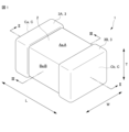
- FIG. 1 is a schematic perspective view of a laminated ceramic capacitor 1 of an embodiment
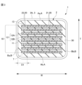
- FIG. 2 is a cross-sectional view of the multilayer ceramic capacitor 1 of FIG. 1 taken along line II-II.
- FIG. 2 is a cross-sectional view of the multilayer ceramic capacitor 1 of FIG. 1 taken along line III-III.
- FIG. 4 is a flow chart explaining an example of a method for manufacturing the multilayer ceramic capacitor 1.
- FIG. 3A to 3C are diagrams for explaining steps up to manufacturing a laminated sheet 103 in the manufacturing method of the multilayer ceramic capacitor 1.
- FIG. FIG. 3 is a diagram for explaining a lamination step in the manufacturing method of the multilayer ceramic capacitor 1;
- FIG. 1 is a schematic perspective view of a laminated ceramic capacitor 1 of an embodiment.
- FIG. 2 is a cross-sectional view of the multilayer ceramic capacitor 1 of FIG. 1 taken along line II-II.
- FIG. 3 is a cross-sectional view of the multilayer ceramic capacitor 1 of FIG. 1 taken along line III-III.
- a laminated ceramic capacitor 1 includes a laminate 2 and a pair of external electrodes 3 provided at both ends of the laminate 2 .
- the laminate 2 includes an inner layer portion 10 in which dielectric layers 11 and internal electrode layers 12 are alternately laminated.
- the direction in which the pair of external electrodes 3 are provided in the multilayer ceramic capacitor 1 is defined as the length direction L as a term that indicates the orientation of the multilayer ceramic capacitor 1 .
- the direction in which the dielectric layers 11 and the internal electrode layers 12 are stacked is defined as a stacking direction T.
- a direction crossing both the length direction L and the stacking direction T is defined as a width direction W.
- the width direction W is orthogonal to both the length direction L and the stacking direction T.
- the stacking direction T is also referred to as a thickness direction.
- the multilayer ceramic capacitor 1 has a withstand voltage of, for example, about 25V.
- the multilayer ceramic capacitor 1 has a substantially rectangular parallelepiped shape, a length direction L dimension of 0.6 mm or more and 3.2 mm or less, a width direction W dimension of 0.3 mm or more and 2.5 mm or less, and a thickness direction (laminating direction). T) The dimension is 0.3 mm or more and 2.5 mm or less.
- the multilayer ceramic capacitor 1 has a chip size of 1005 to 2012, a length direction L dimension of 1.0 mm or more and 2.0 mm or less, and a width direction W dimension and a thickness direction (stacking direction T) dimension of 0.0 mm. It is preferably 5 mm or more and 1.25 mm or less.
- a pair of outer surfaces facing in the lamination direction T are referred to as a first main surface Aa and a second main surface Ab
- a pair of outer surfaces facing in the width direction W The outer surfaces are defined as a first side surface Ba and a second side surface Bb
- a pair of outer surfaces facing each other in the length direction L are defined as a first end surface Ca and a second end surface Cb.
- the first main surface Aa and the second main surface Ab they will be collectively referred to as the main surface A, and the first side surface Ba and the second side surface Bb will need to be specifically distinguished for explanation. If not, they will be collectively referred to as the side surface B, and the first end surface Ca and the second end surface Cb will be collectively described as the end surface C unless it is necessary to distinguish them for description.
- the laminate 2 includes an inner layer portion 10, outer layer portions 13 arranged on both sides of the inner layer portion 10 in the lamination direction T, and side gap portions 30 provided on both sides of the inner layer portion 10 and the outer layer portion 13 in the width direction W. and
- Inner layer portion 10 In the inner layer portion 10, dielectric layers 11 and internal electrode layers 12 are alternately laminated one by one.
- the dielectric layer 11 is formed by, for example, adding a binder, a plasticizer, a dispersant, etc. to a mixture obtained by adding and mixing a ceramic powder such as BaTiO 3 , a glass component, and a sintering aid as necessary.
- a ceramic green sheet obtained by molding a slurry containing an agent and an organic solvent into a sheet is sintered.
- the thickness of the dielectric layer 11 is, for example, 0.8 ⁇ m or more and 4.1 ⁇ m or less, preferably 0.8 ⁇ m or more and 2.0 ⁇ m or less.
- the number of dielectric layers 11 is, for example, 200 or more and 650 or less.
- the internal electrode layer 12 is obtained by sintering an internal electrode layer paste containing a powder of the first metal component, which is the main component, a binder, additives such as a plasticizer and a dispersant, an organic solvent, and the like. is.
- the first metal component that is the main component of the internal electrode layer 12 is Ni in the embodiment, and the first metal component is hereinafter described as Ni.
- the internal electrode layers 12 include a plurality of first internal electrode layers 12A and a plurality of second internal electrode layers 12B.
- the first internal electrode layers 12A and the second internal electrode layers 12B are alternately arranged.
- the thickness of the internal electrode layer 12 is, for example, 0.5 ⁇ m or more and 1.2 ⁇ m or less, preferably 0.5 ⁇ m or more and 0.85 ⁇ m or less.
- the number of the internal electrode layers 12 is, for example, 200 or more and 650 or less, including the first internal electrode layers 12A and the second internal electrode layers 12B.
- the first internal electrode layer 12A includes a first facing portion 12Aa facing the second internal electrode layer 12B, and a first lead portion 12Ab drawn from the first facing portion 12Aa toward the first end surface Ca. An end portion of the first lead-out portion 12Ab is exposed on the first end surface Ca and electrically connected to a first external electrode 3A, which will be described later.
- the second internal electrode layer 12B includes a second facing portion 12Ba facing the first internal electrode layer 12A, and a second lead portion 12Bb drawn from the second facing portion 12Ba to the second end face Cb. An end portion of the second lead portion 12Bb is electrically connected to a second external electrode 3B, which will be described later. Charges are accumulated in the first facing portion 12Aa of the first internal electrode layer 12A and the second facing portion 12Ba of the second internal electrode layer 12B.
- first facing portion 12Aa and the second facing portion 12Ba do not need to be distinguished from each other, they will be collectively referred to as the facing portion 12a, and the first lead-out portion 12Ab and the second lead-out portion 12Bb will be specifically referred to. When there is no need to distinguish and explain, they will be collectively explained as the drawer portion 12b.
- Solid solution layer 20 On both sides of the internal electrode layer 12 in the stacking direction T, at the interface with the dielectric layer 11 or the outer layer portion 13, a solid solution of a second metal component different from the first metal component dissolved in Ni, which is the first metal component, is formed.
- a solvent layer 20 is provided.
- the solid solution layer 20 includes a central solid solution layer 21 and an outer solid solution layer 22 .
- the second metal component is preferably Sn, In, Ga, Zn, Bi, Pb, Fe, V, Y, or Cu.
- the second metal component is Sn. Sn.
- the solid solution layer 20 is a layer in which Sn atoms are randomly substituted for Ni within the Ni atomic arrangement structure while maintaining the Ni atomic arrangement structure.
- the thickness of the solid solution layer 20 is preferably 1 nm or more and 20 nm or less.
- the solid solution layers 20 are provided at the interfaces on both sides of the internal electrode layers 12 in the stacking direction T, but the present invention is not limited to this. It may be provided only at the interface. In the embodiment, the solid solution layer 20 is provided on all the internal electrode layers 12 , but the present invention is not limited to this, and the solid solution layer 20 may be provided only on some of the internal electrode layers 12 .
- the central solid solution layer 21 is provided at the interface between the internal electrode layer 12 and the dielectric layer 11 or the outer layer portion 13 in the central region in the length direction L and width direction W of the laminate 2 .
- Sn is dissolved in Ni at a higher rate than in the outer solid-solution layer 22 .
- the interface is not only a boundary, but also a region that may include a part of the internal electrode layer 12 and the dielectric layer 11 or the outer layer portion 13 .
- the central solid solution layer 21 is a region inside a distance D1 from the end of the length direction L of the facing portion 12a and the end of the width direction W of the facing portion 12a. Distance D1 is about 10 ⁇ m in an embodiment.
- Sn is dissolved in a molar amount of 0.008 or more and 0.025 or less, preferably about 0.02, that is, 2 mol % with respect to the total molar amount of Ni and Sn.
- the ratio of Sn to Ni is a value obtained by measuring 10 interfaces at the central portion in the lamination direction T, the central portion in the width direction W, and the central portion in the length direction L by TEM analysis and averaging the values.
- the outer solid solution layer 22 is provided in a region surrounding the central solid solution layer 21 in the facing portion 12a. That is, the outer solid-solution layer 22 is a region extending from the end in the length direction L of the facing portion 12a and the end in the width direction W of the facing portion 12a to the distance D1.
- Sn dissolves in a molar amount of 0.001 or more and 0.005 or less, preferably about 0.005, that is, 0.5 mol% with respect to the total molar amount of Ni and Sn. ing.
- outer layer portion 13 The outer layer portions 13 are provided on both sides of the inner layer portion 10 in the stacking direction T, and are made of the same dielectric ceramic material as the dielectric layer 11 .
- the side gap portions 30 are provided on both sides of the inner layer portion 10 and the outer layer portion 13 in the width direction W, and are made of the same dielectric ceramic material as the dielectric layer 11 .
- the external electrodes 3 are provided on both end surfaces C of the laminate 2 .
- the external electrode 3 covers not only the end surface C, but also the main surface A and part of the side surface B on the end surface C side.
- the end of the first lead-out portion 12Ab of the first internal electrode layer 12A is exposed on the first end surface Ca and electrically connected to the first external electrode 3A.
- the end of the second lead-out portion 12Bb of the second internal electrode layer 12B is exposed on the second end surface Cb and electrically connected to the second external electrode 3B.
- a plurality of capacitor elements are electrically connected in parallel between the first external electrode 3A and the second external electrode 3B.
- FIG. 4 is a flow chart illustrating an example of a method for manufacturing the multilayer ceramic capacitor 1. As shown in FIG. This manufacturing method is an example, and the present invention is not limited to this.
- 5A and 5B are diagrams for explaining steps up to manufacturing a laminated sheet 103, which will be described later, in the manufacturing method of the multilayer ceramic capacitor 1.
- FIG. The process up to the production of this laminated sheet 103 is also an example, and the present invention is not limited to this.
- Ceramic green sheet production step S1 First, a ceramic slurry containing ceramic powder, a binder and a solvent is prepared. This ceramic slurry is printed in a sheet form on a carrier film using a die coater, a gravure coater, a micro gravure coater, or the like, to produce a ceramic green sheet 101 for the inner layer shown in FIG. 5(a).
- the one side solid solution layer paste printing step S2 includes a center solid solution layer paste printing step S21 and an outer solid solution layer paste printing step S22.
- the central solid-solution layer paste 21P is printed on the surface of the ceramic green sheet 101 for the inner layer portion.
- the central solid-solution layer paste 21P is printed on the central region in the length direction L and the width direction W of each laminate 2 when the laminate 2 is manufactured.
- the central region is a region inside the position of the distance D1, which is 10 ⁇ m in the embodiment, from the end faces C on both sides in the length direction L of the laminate 2 and the side faces B on both sides in the width direction W of the laminate 2 .
- the central solid solution layer paste 21P dissolves Sn in a molar amount of 0.008 or more and 0.025 or less, preferably about 0.02, that is, 2 mol % with respect to the total molar amount of Ni and Sn. ing.
- the ratio of Sn to Ni in the central solid solution layer paste is substantially the same before and after firing.
- the outer solid-solution layer paste 22P is printed on the surface of the inner layer portion ceramic green sheet 101 .
- the outer solid-solution layer paste 22P is positioned outside the position of the distance D1 from the end faces C on both sides in the length direction L of the laminate 2 and the side faces B on both sides in the width direction W of the laminate 2 surrounding the central region. Printed on the peripheral area.
- the outer solid solution layer paste 22P contains Sn in a molar amount of 0.001 or more and 0.005 or less, preferably about 0.005, that is, 0.5 mol % with respect to the total molar amount of Ni and Sn.
- the ratio of Sn to Ni contained in the outer solid solution layer paste 22P is lower than the ratio of Sn to Ni contained in the central solid solution layer paste 21P.
- the other side paste printing step S4 also includes a central solid solution layer paste printing step S41 and an outer solid solution layer paste printing step S42, similarly to the one side solid solution layer paste printing step S2.
- FIG. 6 is a diagram for explaining the lamination process. As shown in the figure, a plurality of laminate sheets 103 are stacked such that the regions printed with the solid-solution layer paste 20P and the internal electrode layer paste 102 are shifted by half a pitch between adjacent laminate sheets 103. be done. Furthermore, ceramic green sheets 112 for outer layer portions are stacked on both sides of the laminated sheet 103 in which a plurality of laminated sheets are laminated.
- Thermal compression step S6 Subsequently, the ceramic green sheet 112 for the outer layer portion and the plurality of stacked laminated sheets 103 are thermocompression bonded. Thereby, the mother block 110 is formed.
- the laminate 2 having the external electrodes 3 formed thereon is heated at the set firing temperature in a nitrogen atmosphere for a predetermined time. Thereby, the multilayer ceramic capacitor 1 is manufactured. At this time, the ceramic green sheets 101 for the inner layer and the ceramic green sheets 112 for the outer layer are sintered into ceramics, and the dielectric layer 11 and the outer layer 13 are formed.
- the internal electrode layer paste 102 becomes the internal electrode layer 12, but the central solid-solution layer paste 21P printed on both sides of the internal electrode layer paste 102 in the stacking direction T is heated to become a central solid.
- the outer solid-solution layer paste 22 ⁇ /b>P becomes the outer solid-solution layer 22 when heated.
- Sn dissolves in a molar amount of 0.008 or more and 0.025 or less, preferably about 0.02, that is, 2 mol % with respect to the total molar amount of Ni and Sn.
- Sn dissolves in a molar amount of 0.001 or more and 0.005 or less, preferably about 0.005, that is, 0.5 mol% with respect to the total molar amount of Ni and Sn. .
- the strength of the internal electrode layers 12 is improved by forming the solid-solution layers 20 on both sides of the internal electrode layers 12 in the lamination direction T. performance (voltage resistance) is improved.
- the solid solution of Sn in Ni changes the state (electrical barrier height) of the internal electrode layer 12 near the interface with the dielectric layer 11, and the high temperature load life can be improved. As described above, it is possible to obtain the multilayer ceramic capacitor 1 having excellent reliability when a voltage is applied.
- Sn has a molar amount of 0.008 or more and 0.025 or less, preferably about 0.02 with respect to the total molar amount of Ni and Sn, That is, 2 mol % is solid-dissolved.
- Sn dissolves in a molar amount of 0.001 or more and 0.005 or less, preferably about 0.005, that is, 0.5 mol% with respect to the total molar amount of Ni and Sn. ing. That is, in the solid solution layer 20 , the central solid solution layer 21 , which is the middle region, has a higher Sn content than the outer solid solution layer 22 . Therefore, the central region of the internal electrode layers 12 can be particularly reinforced.
Landscapes
- Engineering & Computer Science (AREA)
- Power Engineering (AREA)
- Manufacturing & Machinery (AREA)
- Microelectronics & Electronic Packaging (AREA)
- Chemical & Material Sciences (AREA)
- Materials Engineering (AREA)
- Ceramic Engineering (AREA)
- Inorganic Chemistry (AREA)
- Ceramic Capacitors (AREA)
- Fixed Capacitors And Capacitor Manufacturing Machines (AREA)
Priority Applications (3)
| Application Number | Priority Date | Filing Date | Title |
|---|---|---|---|
| JP2023574044A JP7697536B2 (ja) | 2022-01-17 | 2023-01-11 | 電子部品 |
| CN202380016931.8A CN118648074A (zh) | 2022-01-17 | 2023-01-11 | 电子部件 |
| US18/667,273 US12562310B2 (en) | 2022-01-17 | 2024-05-17 | Electronic component |
Applications Claiming Priority (2)
| Application Number | Priority Date | Filing Date | Title |
|---|---|---|---|
| JP2022004907 | 2022-01-17 | ||
| JP2022-004907 | 2022-01-17 |
Related Child Applications (1)
| Application Number | Title | Priority Date | Filing Date |
|---|---|---|---|
| US18/667,273 Continuation US12562310B2 (en) | 2022-01-17 | 2024-05-17 | Electronic component |
Publications (1)
| Publication Number | Publication Date |
|---|---|
| WO2023136258A1 true WO2023136258A1 (ja) | 2023-07-20 |
Family
ID=87279185
Family Applications (1)
| Application Number | Title | Priority Date | Filing Date |
|---|---|---|---|
| PCT/JP2023/000416 Ceased WO2023136258A1 (ja) | 2022-01-17 | 2023-01-11 | 電子部品 |
Country Status (4)
| Country | Link |
|---|---|
| US (1) | US12562310B2 (https=) |
| JP (1) | JP7697536B2 (https=) |
| CN (1) | CN118648074A (https=) |
| WO (1) | WO2023136258A1 (https=) |
Cited By (1)
| Publication number | Priority date | Publication date | Assignee | Title |
|---|---|---|---|---|
| US12562314B2 (en) * | 2021-12-28 | 2026-02-24 | Murata Manufacturing Co., Ltd. | Electronic component |
Families Citing this family (1)
| Publication number | Priority date | Publication date | Assignee | Title |
|---|---|---|---|---|
| JP2024055118A (ja) * | 2022-10-06 | 2024-04-18 | 太陽誘電株式会社 | セラミック電子部品およびその製造方法 |
Citations (3)
| Publication number | Priority date | Publication date | Assignee | Title |
|---|---|---|---|---|
| JP2020031202A (ja) * | 2018-08-23 | 2020-02-27 | サムソン エレクトロ−メカニックス カンパニーリミテッド. | 積層セラミック電子部品及びその製造方法 |
| JP2021034648A (ja) * | 2019-08-28 | 2021-03-01 | 株式会社村田製作所 | 積層セラミックコンデンサ |
| JP2021108360A (ja) * | 2019-12-27 | 2021-07-29 | 株式会社村田製作所 | 積層セラミックコンデンサ |
Family Cites Families (6)
| Publication number | Priority date | Publication date | Assignee | Title |
|---|---|---|---|---|
| JP7133908B2 (ja) | 2017-06-22 | 2022-09-09 | 太陽誘電株式会社 | 積層セラミックコンデンサ |
| KR102736492B1 (ko) | 2019-12-27 | 2024-11-29 | 가부시키가이샤 무라타 세이사쿠쇼 | 적층 세라믹 콘덴서 |
| US11367573B2 (en) * | 2019-12-27 | 2022-06-21 | Murata Manufacturing Co., Ltd. | Multilayer ceramic capacitor |
| JP2021190484A (ja) * | 2020-05-26 | 2021-12-13 | 株式会社村田製作所 | 積層セラミック電子部品及びその製造方法 |
| JP2022057919A (ja) * | 2020-09-30 | 2022-04-11 | 株式会社村田製作所 | 積層セラミックコンデンサ |
| JP7459858B2 (ja) * | 2021-12-23 | 2024-04-02 | 株式会社村田製作所 | 積層セラミックコンデンサおよび積層セラミックコンデンサの実装構造 |
-
2023
- 2023-01-11 JP JP2023574044A patent/JP7697536B2/ja active Active
- 2023-01-11 WO PCT/JP2023/000416 patent/WO2023136258A1/ja not_active Ceased
- 2023-01-11 CN CN202380016931.8A patent/CN118648074A/zh active Pending
-
2024
- 2024-05-17 US US18/667,273 patent/US12562310B2/en active Active
Patent Citations (3)
| Publication number | Priority date | Publication date | Assignee | Title |
|---|---|---|---|---|
| JP2020031202A (ja) * | 2018-08-23 | 2020-02-27 | サムソン エレクトロ−メカニックス カンパニーリミテッド. | 積層セラミック電子部品及びその製造方法 |
| JP2021034648A (ja) * | 2019-08-28 | 2021-03-01 | 株式会社村田製作所 | 積層セラミックコンデンサ |
| JP2021108360A (ja) * | 2019-12-27 | 2021-07-29 | 株式会社村田製作所 | 積層セラミックコンデンサ |
Cited By (1)
| Publication number | Priority date | Publication date | Assignee | Title |
|---|---|---|---|---|
| US12562314B2 (en) * | 2021-12-28 | 2026-02-24 | Murata Manufacturing Co., Ltd. | Electronic component |
Also Published As
| Publication number | Publication date |
|---|---|
| CN118648074A (zh) | 2024-09-13 |
| US20240304388A1 (en) | 2024-09-12 |
| JP7697536B2 (ja) | 2025-06-24 |
| US12562310B2 (en) | 2026-02-24 |
| JPWO2023136258A1 (https=) | 2023-07-20 |
Similar Documents
| Publication | Publication Date | Title |
|---|---|---|
| US11557433B2 (en) | Multilayer ceramic capacitor having certain thickness ratio of external electrode to cover layer | |
| US20240312712A1 (en) | Electronic component | |
| JP7231340B2 (ja) | セラミック電子部品およびその製造方法 | |
| KR101983129B1 (ko) | 적층 세라믹 전자부품 및 이의 제조방법 | |
| JP2020057738A (ja) | 電子部品、回路基板、および電子部品の回路基板への実装方法 | |
| JP2016001721A (ja) | 積層セラミックコンデンサ | |
| JP2023156502A (ja) | 積層セラミックコンデンサ | |
| JP2020053577A (ja) | 電子部品 | |
| KR20120133716A (ko) | 적층 세라믹 커패시터 | |
| US9281121B2 (en) | Multilayer ceramic electronic component and manufacturing method thereof | |
| US12562310B2 (en) | Electronic component | |
| KR20170077548A (ko) | 적층 세라믹 전자부품 및 이의 제조방법 | |
| KR102002388B1 (ko) | 전자부품 | |
| JP2022016003A (ja) | 電子部品 | |
| JP2023109441A (ja) | 3端子型積層セラミックコンデンサ | |
| JP7616431B2 (ja) | 電子部品 | |
| US12562314B2 (en) | Electronic component | |
| US20140126109A1 (en) | Multilayer ceramic electronic component and fabricating method thereof | |
| JP2022016002A (ja) | 電子部品 | |
| KR102881785B1 (ko) | 적층형 전자 부품 | |
| US20260058058A1 (en) | Multilayer ceramic capacitor | |
| CN217562410U (zh) | 层叠陶瓷电容器 | |
| KR20140077347A (ko) | 적층 세라믹 전자부품 및 이의 제조방법 | |
| KR102473420B1 (ko) | 적층 세라믹 전자부품 | |
| WO2024162392A1 (ja) | セラミック電子部品およびその製造方法 |
Legal Events
| Date | Code | Title | Description |
|---|---|---|---|
| 121 | Ep: the epo has been informed by wipo that ep was designated in this application |
Ref document number: 23740267 Country of ref document: EP Kind code of ref document: A1 |
|
| WWE | Wipo information: entry into national phase |
Ref document number: 2023574044 Country of ref document: JP |
|
| WWE | Wipo information: entry into national phase |
Ref document number: 202380016931.8 Country of ref document: CN |
|
| NENP | Non-entry into the national phase |
Ref country code: DE |
|
| 122 | Ep: pct application non-entry in european phase |
Ref document number: 23740267 Country of ref document: EP Kind code of ref document: A1 |