WO2023136258A1 - 電子部品 - Google Patents
電子部品 Download PDFInfo
- Publication number
- WO2023136258A1 WO2023136258A1 PCT/JP2023/000416 JP2023000416W WO2023136258A1 WO 2023136258 A1 WO2023136258 A1 WO 2023136258A1 JP 2023000416 W JP2023000416 W JP 2023000416W WO 2023136258 A1 WO2023136258 A1 WO 2023136258A1
- Authority
- WO
- WIPO (PCT)
- Prior art keywords
- layer
- solid
- metal component
- solution layer
- internal electrode
- Prior art date
Links
- 239000006104 solid solution Substances 0.000 claims abstract description 92
- 239000002184 metal Substances 0.000 claims abstract description 31
- 229910052751 metal Inorganic materials 0.000 claims abstract description 31
- 229910052718 tin Inorganic materials 0.000 claims description 10
- 229910052797 bismuth Inorganic materials 0.000 claims description 2
- 229910052733 gallium Inorganic materials 0.000 claims description 2
- 229910052738 indium Inorganic materials 0.000 claims description 2
- 229910052742 iron Inorganic materials 0.000 claims description 2
- 229910052745 lead Inorganic materials 0.000 claims description 2
- 229910052720 vanadium Inorganic materials 0.000 claims description 2
- 229910052727 yttrium Inorganic materials 0.000 claims description 2
- 229910052725 zinc Inorganic materials 0.000 claims description 2
- 229910052802 copper Inorganic materials 0.000 claims 1
- 239000003985 ceramic capacitor Substances 0.000 description 22
- 239000000919 ceramic Substances 0.000 description 14
- 238000004519 manufacturing process Methods 0.000 description 11
- 238000003475 lamination Methods 0.000 description 9
- 229910052759 nickel Inorganic materials 0.000 description 8
- 238000005520 cutting process Methods 0.000 description 4
- 238000010586 diagram Methods 0.000 description 4
- 238000000034 method Methods 0.000 description 4
- 239000011230 binding agent Substances 0.000 description 3
- 238000010304 firing Methods 0.000 description 3
- 239000000843 powder Substances 0.000 description 3
- 239000002002 slurry Substances 0.000 description 3
- 229910010293 ceramic material Inorganic materials 0.000 description 2
- 239000002270 dispersing agent Substances 0.000 description 2
- 239000003960 organic solvent Substances 0.000 description 2
- 230000002093 peripheral effect Effects 0.000 description 2
- 239000004014 plasticizer Substances 0.000 description 2
- 238000005245 sintering Methods 0.000 description 2
- 239000002904 solvent Substances 0.000 description 2
- 238000012935 Averaging Methods 0.000 description 1
- 239000000654 additive Substances 0.000 description 1
- 230000004888 barrier function Effects 0.000 description 1
- 230000015572 biosynthetic process Effects 0.000 description 1
- 239000003990 capacitor Substances 0.000 description 1
- 239000003795 chemical substances by application Substances 0.000 description 1
- 230000006835 compression Effects 0.000 description 1
- 238000007906 compression Methods 0.000 description 1
- 239000011521 glass Substances 0.000 description 1
- 238000010030 laminating Methods 0.000 description 1
- 239000000203 mixture Substances 0.000 description 1
- 238000000465 moulding Methods 0.000 description 1
- 239000012299 nitrogen atmosphere Substances 0.000 description 1
- 239000007787 solid Substances 0.000 description 1
Images


Classifications
-
- H—ELECTRICITY
- H01—ELECTRIC ELEMENTS
- H01G—CAPACITORS; CAPACITORS, RECTIFIERS, DETECTORS, SWITCHING DEVICES, LIGHT-SENSITIVE OR TEMPERATURE-SENSITIVE DEVICES OF THE ELECTROLYTIC TYPE
- H01G4/00—Fixed capacitors; Processes of their manufacture
- H01G4/30—Stacked capacitors
Definitions
- the present invention relates to electronic components.
- an electronic component which is a multilayer ceramic capacitor, includes a laminate in which a plurality of dielectric layers and a plurality of internal electrode layers are alternately laminated, and two end faces provided on both sides in the length direction of the laminate. and two external electrodes arranged respectively (see Patent Document 1).
- An object of the present invention is to provide an electronic component that is highly reliable when a voltage is applied.
- the present invention provides a dielectric layer having a thickness of 0.8 ⁇ m or more and 4.1 ⁇ m or less and an internal electrode layer having a thickness of 0.5 ⁇ m or more and 1.2 ⁇ m or less alternately laminated,
- An electronic component comprising a laminate in which the number of each of the dielectric layers and the number of the internal electrode layers is 200 or more and 650 or less, wherein the internal electrode layer is provided at an interface between the internal electrode layer and the dielectric layer.
- a solid solution layer is provided in which a second metal component different from the first metal component is dissolved in the first metal component which is the main component of the solid solution layer, and the solid solution layers are opposed to each other between the adjacent internal electrode layers
- a central solid-solution layer located 10 ⁇ m or more inward from the ends in the length direction and the width direction of the facing portion, and an outer solid-solution layer surrounding the central solid-solution layer, wherein the central solid-solution layer is and an electronic component in which the solid solution ratio of the second metal component to the first metal component is higher than that of the outer solid solution layer.
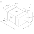
- FIG. 1 is a schematic perspective view of a laminated ceramic capacitor 1 of an embodiment
- FIG. 2 is a cross-sectional view of the multilayer ceramic capacitor 1 of FIG. 1 taken along line II-II.
- FIG. 2 is a cross-sectional view of the multilayer ceramic capacitor 1 of FIG. 1 taken along line III-III.
- FIG. 4 is a flow chart explaining an example of a method for manufacturing the multilayer ceramic capacitor 1.
- FIG. 3A to 3C are diagrams for explaining steps up to manufacturing a laminated sheet 103 in the manufacturing method of the multilayer ceramic capacitor 1.
- FIG. FIG. 3 is a diagram for explaining a lamination step in the manufacturing method of the multilayer ceramic capacitor 1;
- FIG. 1 is a schematic perspective view of a laminated ceramic capacitor 1 of an embodiment.
- FIG. 2 is a cross-sectional view of the multilayer ceramic capacitor 1 of FIG. 1 taken along line II-II.
- FIG. 3 is a cross-sectional view of the multilayer ceramic capacitor 1 of FIG. 1 taken along line III-III.
- a laminated ceramic capacitor 1 includes a laminate 2 and a pair of external electrodes 3 provided at both ends of the laminate 2 .
- the laminate 2 includes an inner layer portion 10 in which dielectric layers 11 and internal electrode layers 12 are alternately laminated.
- the direction in which the pair of external electrodes 3 are provided in the multilayer ceramic capacitor 1 is defined as the length direction L as a term that indicates the orientation of the multilayer ceramic capacitor 1 .
- the direction in which the dielectric layers 11 and the internal electrode layers 12 are stacked is defined as a stacking direction T.
- a direction crossing both the length direction L and the stacking direction T is defined as a width direction W.
- the width direction W is orthogonal to both the length direction L and the stacking direction T.
- the stacking direction T is also referred to as a thickness direction.
- the multilayer ceramic capacitor 1 has a withstand voltage of, for example, about 25V.
- the multilayer ceramic capacitor 1 has a substantially rectangular parallelepiped shape, a length direction L dimension of 0.6 mm or more and 3.2 mm or less, a width direction W dimension of 0.3 mm or more and 2.5 mm or less, and a thickness direction (laminating direction). T) The dimension is 0.3 mm or more and 2.5 mm or less.
- the multilayer ceramic capacitor 1 has a chip size of 1005 to 2012, a length direction L dimension of 1.0 mm or more and 2.0 mm or less, and a width direction W dimension and a thickness direction (stacking direction T) dimension of 0.0 mm. It is preferably 5 mm or more and 1.25 mm or less.
- a pair of outer surfaces facing in the lamination direction T are referred to as a first main surface Aa and a second main surface Ab
- a pair of outer surfaces facing in the width direction W The outer surfaces are defined as a first side surface Ba and a second side surface Bb
- a pair of outer surfaces facing each other in the length direction L are defined as a first end surface Ca and a second end surface Cb.
- the first main surface Aa and the second main surface Ab they will be collectively referred to as the main surface A, and the first side surface Ba and the second side surface Bb will need to be specifically distinguished for explanation. If not, they will be collectively referred to as the side surface B, and the first end surface Ca and the second end surface Cb will be collectively described as the end surface C unless it is necessary to distinguish them for description.
- the laminate 2 includes an inner layer portion 10, outer layer portions 13 arranged on both sides of the inner layer portion 10 in the lamination direction T, and side gap portions 30 provided on both sides of the inner layer portion 10 and the outer layer portion 13 in the width direction W. and
- Inner layer portion 10 In the inner layer portion 10, dielectric layers 11 and internal electrode layers 12 are alternately laminated one by one.
- the dielectric layer 11 is formed by, for example, adding a binder, a plasticizer, a dispersant, etc. to a mixture obtained by adding and mixing a ceramic powder such as BaTiO 3 , a glass component, and a sintering aid as necessary.
- a ceramic green sheet obtained by molding a slurry containing an agent and an organic solvent into a sheet is sintered.
- the thickness of the dielectric layer 11 is, for example, 0.8 ⁇ m or more and 4.1 ⁇ m or less, preferably 0.8 ⁇ m or more and 2.0 ⁇ m or less.
- the number of dielectric layers 11 is, for example, 200 or more and 650 or less.
- the internal electrode layer 12 is obtained by sintering an internal electrode layer paste containing a powder of the first metal component, which is the main component, a binder, additives such as a plasticizer and a dispersant, an organic solvent, and the like. is.
- the first metal component that is the main component of the internal electrode layer 12 is Ni in the embodiment, and the first metal component is hereinafter described as Ni.
- the internal electrode layers 12 include a plurality of first internal electrode layers 12A and a plurality of second internal electrode layers 12B.
- the first internal electrode layers 12A and the second internal electrode layers 12B are alternately arranged.
- the thickness of the internal electrode layer 12 is, for example, 0.5 ⁇ m or more and 1.2 ⁇ m or less, preferably 0.5 ⁇ m or more and 0.85 ⁇ m or less.
- the number of the internal electrode layers 12 is, for example, 200 or more and 650 or less, including the first internal electrode layers 12A and the second internal electrode layers 12B.
- the first internal electrode layer 12A includes a first facing portion 12Aa facing the second internal electrode layer 12B, and a first lead portion 12Ab drawn from the first facing portion 12Aa toward the first end surface Ca. An end portion of the first lead-out portion 12Ab is exposed on the first end surface Ca and electrically connected to a first external electrode 3A, which will be described later.
- the second internal electrode layer 12B includes a second facing portion 12Ba facing the first internal electrode layer 12A, and a second lead portion 12Bb drawn from the second facing portion 12Ba to the second end face Cb. An end portion of the second lead portion 12Bb is electrically connected to a second external electrode 3B, which will be described later. Charges are accumulated in the first facing portion 12Aa of the first internal electrode layer 12A and the second facing portion 12Ba of the second internal electrode layer 12B.
- first facing portion 12Aa and the second facing portion 12Ba do not need to be distinguished from each other, they will be collectively referred to as the facing portion 12a, and the first lead-out portion 12Ab and the second lead-out portion 12Bb will be specifically referred to. When there is no need to distinguish and explain, they will be collectively explained as the drawer portion 12b.
- Solid solution layer 20 On both sides of the internal electrode layer 12 in the stacking direction T, at the interface with the dielectric layer 11 or the outer layer portion 13, a solid solution of a second metal component different from the first metal component dissolved in Ni, which is the first metal component, is formed.
- a solvent layer 20 is provided.
- the solid solution layer 20 includes a central solid solution layer 21 and an outer solid solution layer 22 .
- the second metal component is preferably Sn, In, Ga, Zn, Bi, Pb, Fe, V, Y, or Cu.
- the second metal component is Sn. Sn.
- the solid solution layer 20 is a layer in which Sn atoms are randomly substituted for Ni within the Ni atomic arrangement structure while maintaining the Ni atomic arrangement structure.
- the thickness of the solid solution layer 20 is preferably 1 nm or more and 20 nm or less.
- the solid solution layers 20 are provided at the interfaces on both sides of the internal electrode layers 12 in the stacking direction T, but the present invention is not limited to this. It may be provided only at the interface. In the embodiment, the solid solution layer 20 is provided on all the internal electrode layers 12 , but the present invention is not limited to this, and the solid solution layer 20 may be provided only on some of the internal electrode layers 12 .
- the central solid solution layer 21 is provided at the interface between the internal electrode layer 12 and the dielectric layer 11 or the outer layer portion 13 in the central region in the length direction L and width direction W of the laminate 2 .
- Sn is dissolved in Ni at a higher rate than in the outer solid-solution layer 22 .
- the interface is not only a boundary, but also a region that may include a part of the internal electrode layer 12 and the dielectric layer 11 or the outer layer portion 13 .
- the central solid solution layer 21 is a region inside a distance D1 from the end of the length direction L of the facing portion 12a and the end of the width direction W of the facing portion 12a. Distance D1 is about 10 ⁇ m in an embodiment.
- Sn is dissolved in a molar amount of 0.008 or more and 0.025 or less, preferably about 0.02, that is, 2 mol % with respect to the total molar amount of Ni and Sn.
- the ratio of Sn to Ni is a value obtained by measuring 10 interfaces at the central portion in the lamination direction T, the central portion in the width direction W, and the central portion in the length direction L by TEM analysis and averaging the values.
- the outer solid solution layer 22 is provided in a region surrounding the central solid solution layer 21 in the facing portion 12a. That is, the outer solid-solution layer 22 is a region extending from the end in the length direction L of the facing portion 12a and the end in the width direction W of the facing portion 12a to the distance D1.
- Sn dissolves in a molar amount of 0.001 or more and 0.005 or less, preferably about 0.005, that is, 0.5 mol% with respect to the total molar amount of Ni and Sn. ing.
- outer layer portion 13 The outer layer portions 13 are provided on both sides of the inner layer portion 10 in the stacking direction T, and are made of the same dielectric ceramic material as the dielectric layer 11 .
- the side gap portions 30 are provided on both sides of the inner layer portion 10 and the outer layer portion 13 in the width direction W, and are made of the same dielectric ceramic material as the dielectric layer 11 .
- the external electrodes 3 are provided on both end surfaces C of the laminate 2 .
- the external electrode 3 covers not only the end surface C, but also the main surface A and part of the side surface B on the end surface C side.
- the end of the first lead-out portion 12Ab of the first internal electrode layer 12A is exposed on the first end surface Ca and electrically connected to the first external electrode 3A.
- the end of the second lead-out portion 12Bb of the second internal electrode layer 12B is exposed on the second end surface Cb and electrically connected to the second external electrode 3B.
- a plurality of capacitor elements are electrically connected in parallel between the first external electrode 3A and the second external electrode 3B.
- FIG. 4 is a flow chart illustrating an example of a method for manufacturing the multilayer ceramic capacitor 1. As shown in FIG. This manufacturing method is an example, and the present invention is not limited to this.
- 5A and 5B are diagrams for explaining steps up to manufacturing a laminated sheet 103, which will be described later, in the manufacturing method of the multilayer ceramic capacitor 1.
- FIG. The process up to the production of this laminated sheet 103 is also an example, and the present invention is not limited to this.
- Ceramic green sheet production step S1 First, a ceramic slurry containing ceramic powder, a binder and a solvent is prepared. This ceramic slurry is printed in a sheet form on a carrier film using a die coater, a gravure coater, a micro gravure coater, or the like, to produce a ceramic green sheet 101 for the inner layer shown in FIG. 5(a).
- the one side solid solution layer paste printing step S2 includes a center solid solution layer paste printing step S21 and an outer solid solution layer paste printing step S22.
- the central solid-solution layer paste 21P is printed on the surface of the ceramic green sheet 101 for the inner layer portion.
- the central solid-solution layer paste 21P is printed on the central region in the length direction L and the width direction W of each laminate 2 when the laminate 2 is manufactured.
- the central region is a region inside the position of the distance D1, which is 10 ⁇ m in the embodiment, from the end faces C on both sides in the length direction L of the laminate 2 and the side faces B on both sides in the width direction W of the laminate 2 .
- the central solid solution layer paste 21P dissolves Sn in a molar amount of 0.008 or more and 0.025 or less, preferably about 0.02, that is, 2 mol % with respect to the total molar amount of Ni and Sn. ing.
- the ratio of Sn to Ni in the central solid solution layer paste is substantially the same before and after firing.
- the outer solid-solution layer paste 22P is printed on the surface of the inner layer portion ceramic green sheet 101 .
- the outer solid-solution layer paste 22P is positioned outside the position of the distance D1 from the end faces C on both sides in the length direction L of the laminate 2 and the side faces B on both sides in the width direction W of the laminate 2 surrounding the central region. Printed on the peripheral area.
- the outer solid solution layer paste 22P contains Sn in a molar amount of 0.001 or more and 0.005 or less, preferably about 0.005, that is, 0.5 mol % with respect to the total molar amount of Ni and Sn.
- the ratio of Sn to Ni contained in the outer solid solution layer paste 22P is lower than the ratio of Sn to Ni contained in the central solid solution layer paste 21P.
- the other side paste printing step S4 also includes a central solid solution layer paste printing step S41 and an outer solid solution layer paste printing step S42, similarly to the one side solid solution layer paste printing step S2.
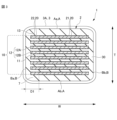
- FIG. 6 is a diagram for explaining the lamination process. As shown in the figure, a plurality of laminate sheets 103 are stacked such that the regions printed with the solid-solution layer paste 20P and the internal electrode layer paste 102 are shifted by half a pitch between adjacent laminate sheets 103. be done. Furthermore, ceramic green sheets 112 for outer layer portions are stacked on both sides of the laminated sheet 103 in which a plurality of laminated sheets are laminated.
- Thermal compression step S6 Subsequently, the ceramic green sheet 112 for the outer layer portion and the plurality of stacked laminated sheets 103 are thermocompression bonded. Thereby, the mother block 110 is formed.
- the laminate 2 having the external electrodes 3 formed thereon is heated at the set firing temperature in a nitrogen atmosphere for a predetermined time. Thereby, the multilayer ceramic capacitor 1 is manufactured. At this time, the ceramic green sheets 101 for the inner layer and the ceramic green sheets 112 for the outer layer are sintered into ceramics, and the dielectric layer 11 and the outer layer 13 are formed.
- the internal electrode layer paste 102 becomes the internal electrode layer 12, but the central solid-solution layer paste 21P printed on both sides of the internal electrode layer paste 102 in the stacking direction T is heated to become a central solid.
- the outer solid-solution layer paste 22 ⁇ /b>P becomes the outer solid-solution layer 22 when heated.
- Sn dissolves in a molar amount of 0.008 or more and 0.025 or less, preferably about 0.02, that is, 2 mol % with respect to the total molar amount of Ni and Sn.
- Sn dissolves in a molar amount of 0.001 or more and 0.005 or less, preferably about 0.005, that is, 0.5 mol% with respect to the total molar amount of Ni and Sn. .
- the strength of the internal electrode layers 12 is improved by forming the solid-solution layers 20 on both sides of the internal electrode layers 12 in the lamination direction T. performance (voltage resistance) is improved.
- the solid solution of Sn in Ni changes the state (electrical barrier height) of the internal electrode layer 12 near the interface with the dielectric layer 11, and the high temperature load life can be improved. As described above, it is possible to obtain the multilayer ceramic capacitor 1 having excellent reliability when a voltage is applied.
- Sn has a molar amount of 0.008 or more and 0.025 or less, preferably about 0.02 with respect to the total molar amount of Ni and Sn, That is, 2 mol % is solid-dissolved.
- Sn dissolves in a molar amount of 0.001 or more and 0.005 or less, preferably about 0.005, that is, 0.5 mol% with respect to the total molar amount of Ni and Sn. ing. That is, in the solid solution layer 20 , the central solid solution layer 21 , which is the middle region, has a higher Sn content than the outer solid solution layer 22 . Therefore, the central region of the internal electrode layers 12 can be particularly reinforced.
Landscapes
- Engineering & Computer Science (AREA)
- Power Engineering (AREA)
- Manufacturing & Machinery (AREA)
- Microelectronics & Electronic Packaging (AREA)
- Fixed Capacitors And Capacitor Manufacturing Machines (AREA)
- Ceramic Capacitors (AREA)
Abstract
電圧印加時における高い信頼性が得られる電子部品を提供する。厚みが0.8μm以上4.1μm以下の誘電体層11と、厚みが0.5μm以上1.2μm以下の内部電極層12とが互いに交互に積層され、誘電体層11及び内部電極層12のそれぞれの枚数が200枚以上650枚以下である積層体2を備える電子部品1であって、内部電極層12と誘電体層11との界面に、内部電極層12の主成分である第1金属成分に、該第1金属成分と異なる第2金属成分が固溶した固溶層20が設けられ、固溶層20は、互いに隣り合う内部電極層12同士で対向する対向部12aにおける、長さ方向、及び幅方向の端部から、10μm以上内側に位置する中央固溶層21と、中央固溶層21を囲む外側固溶層22と、を含み、中央固溶層21は、外側固溶層22よりも、第1金属成分に対する第2金属成分の固溶の割合が大きい。
Description
本発明は、電子部品に関する。
例えば積層セラミックコンデンサである電子部品は、複数の誘電体層と複数の内部電極層とが互いに交互に積層された積層体と、積層体における、長さ方向の両側に設けられた2つの端面にそれぞれ配置された2つの外部電極と、を備える(特許文献1参照)。
このような電子部品は、電圧印加時における高い信頼性が求められている。本発明は、電圧印加時における高い信頼性が得られる電子部品を提供することを目的とする。
上記課題を解決するために、本発明は、厚みが0.8μm以上4.1μm以下の誘電体層と、厚みが0.5μm以上1.2μm以下の内部電極層とが互いに交互に積層され、前記誘電体層及び前記内部電極層のそれぞれの枚数が200枚以上650枚以下である積層体を備える電子部品であって、前記内部電極層と前記誘電体層との界面に、前記内部電極層の主成分である第1金属成分に、該第1金属成分と異なる第2金属成分が固溶した固溶層が設けられ、前記固溶層は、互いに隣り合う前記内部電極層同士で対向する対向部における、長さ方向、及び幅方向の端部から、10μm以上内側に位置する中央固溶層と、前記中央固溶層を囲む外側固溶層と、を含み、前記中央固溶層は、前記外側固溶層よりも、前記第1金属成分に対する前記第2金属成分の固溶の割合が大きい、電子部品を提供する。
本発明によれば、電圧印加時における高い信頼性が得られる電子部品を提供することができる。
以下、本発明の実施形態にかかる積層セラミックコンデンサ1について説明する。図1は、実施形態の積層セラミックコンデンサ1の概略斜視図である。図2は、図1の積層セラミックコンデンサ1のII-II線に沿った断面図である。図3は、図1の積層セラミックコンデンサ1のIII-III線に沿った断面図である。
積層セラミックコンデンサ1は、積層体2と、積層体2の両端に設けられた一対の外部電極3とを備える。積層体2は、誘電体層11と内部電極層12とが、互いに交互に積層された内層部10を含む。
以下の説明において、積層セラミックコンデンサ1の向きを表わす用語として、積層セラミックコンデンサ1において、一対の外部電極3が設けられている方向を長さ方向Lとする。誘電体層11と内部電極層12とが積層されている方向を積層方向Tとする。長さ方向L及び積層方向Tのいずれにも交差する方向を幅方向Wとする。なお、実施形態においては、幅方向Wは長さ方向L及び積層方向Tのいずれにも直交している。また、積層方向Tを厚み方向ともいう。
積層セラミックコンデンサ1は、例えば、耐電圧が25V程度である。そして、積層セラミックコンデンサ1は略直方体形状を有し、長さ方向L寸法が、0.6mm以上3.2mm以下、幅方向W寸法が、0.3mm以上2.5mm以下、厚み方向(積層方向T)寸法が0.3mm以上2.5mm以下である。さらに、積層セラミックコンデンサ1は、チップサイズ1005サイズから2012サイズであって、長さ方向L寸法が1.0mm以上2.0mm以下、幅方向W寸法及び厚み方向(積層方向T)寸法が0.5mm以上1.25mm以下であることが好ましい。
また、以下の説明において、積層体2の6つの外表面のうち、積層方向Tに相対する一対の外表面を第1主面Aaと第2主面Abとし、幅方向Wに相対する一対の外表面を第1側面Baと第2側面Bbとし、長さ方向Lに相対する一対の外表面を第1端面Caと第2端面Cbとする。なお、第1主面Aaと第2主面Abとを特に区別して説明する必要のない場合、まとめて主面Aとし、第1側面Baと第2側面Bbとを特に区別して説明する必要のない場合、まとめて側面Bとし、第1端面Caと第2端面Cbとを特に区別して説明する必要のない場合、まとめて端面Cとして説明する。
(積層体2)
積層体2は、内層部10と、内層部10の積層方向Tの両側にそれぞれ配置された外層部13と、内層部10及び外層部13の幅方向Wの両側に設けられたサイドギャップ部30とを備える。
積層体2は、内層部10と、内層部10の積層方向Tの両側にそれぞれ配置された外層部13と、内層部10及び外層部13の幅方向Wの両側に設けられたサイドギャップ部30とを備える。
(内層部10)
内層部10は、誘電体層11と内部電極層12とが、1枚ずつ交互に積層されている。
内層部10は、誘電体層11と内部電極層12とが、1枚ずつ交互に積層されている。
(誘電体層11)
誘電体層11は、例えば、BaTiO3であるセラミック粉末と、ガラス成分と、必要に応じて焼結助剤と、を添加して混合した混合物に、バインダと、可塑剤や分散剤等の添加剤と、有機溶剤と、を加えたスラリーをシート状に成形して得られたセラミックグリーンシートが焼結されたものである。誘電体層11の厚みは、例えば、0.8μm以上4.1μm以下であり、好ましくは0.8μm以上2.0μm以下である。また、誘電体層11の枚数は、例えば200枚以上650枚以下である。
誘電体層11は、例えば、BaTiO3であるセラミック粉末と、ガラス成分と、必要に応じて焼結助剤と、を添加して混合した混合物に、バインダと、可塑剤や分散剤等の添加剤と、有機溶剤と、を加えたスラリーをシート状に成形して得られたセラミックグリーンシートが焼結されたものである。誘電体層11の厚みは、例えば、0.8μm以上4.1μm以下であり、好ましくは0.8μm以上2.0μm以下である。また、誘電体層11の枚数は、例えば200枚以上650枚以下である。
(内部電極層12)
内部電極層12は、主成分である第1金属成分の粉末と、バインダと、可塑剤や分散剤等の添加剤と、有機溶剤と、等を含む内部電極層用ペーストが焼結されたものである。内部電極層12の主成分である第1金属成分は、実施形態ではNiであり、以下、第1金属成分をNiとして説明する。
内部電極層12は、主成分である第1金属成分の粉末と、バインダと、可塑剤や分散剤等の添加剤と、有機溶剤と、等を含む内部電極層用ペーストが焼結されたものである。内部電極層12の主成分である第1金属成分は、実施形態ではNiであり、以下、第1金属成分をNiとして説明する。
内部電極層12は、複数の第1内部電極層12Aと複数の第2内部電極層12Bとを備える。第1内部電極層12Aと第2内部電極層12Bとは、交互に配置されている。内部電極層12の厚みは、例えば、0.5μm以上1.2μm以下であり、好ましくは0.5μm以上0.85μm以下である。また、内部電極層12の枚数は、第1内部電極層12A及び第2内部電極層12Bを合わせて、例えば200枚以上650枚以下である。
第1内部電極層12Aは、第2内部電極層12Bと対向する第1対向部12Aaと、第1対向部12Aaから第1端面Ca側に引き出された第1引出部12Abとを備える。第1引出部12Abの端部は、第1端面Caに露出し、後述の第1外部電極3Aに電気的に接続されている。
第2内部電極層12Bは、第1内部電極層12Aと対向する第2対向部12Baと、第2対向部12Baから第2端面Cbに引き出された第2引出部12Bbとを備える。第2引出部12Bbの端部は、後述の第2外部電極3Bに電気的に接続されている。
そして、第1内部電極層12Aの第1対向部12Aaと、第2内部電極層12Bの第2対向部12Baとに電荷が蓄積される。
第2内部電極層12Bは、第1内部電極層12Aと対向する第2対向部12Baと、第2対向部12Baから第2端面Cbに引き出された第2引出部12Bbとを備える。第2引出部12Bbの端部は、後述の第2外部電極3Bに電気的に接続されている。
そして、第1内部電極層12Aの第1対向部12Aaと、第2内部電極層12Bの第2対向部12Baとに電荷が蓄積される。
なお、以下、第1対向部12Aaと第2対向部12Baとを特に区別して説明する必要のない場合、まとめて対向部12aとして説明し、第1引出部12Abと第2引出部12Bbとを特に区別して説明する必要のない場合、まとめて引出部12bとして説明する。
(固溶層20)
内部電極層12の積層方向Tの両側の、誘電体層11又は外層部13との界面には、第1金属成分であるNiに、第1金属成分と異なる第2金属成分が固溶した固溶層20が設けられている。固溶層20は、中央固溶層21と外側固溶層22とを含む。
第2金属成分は、Sn、In、Ga、Zn、Bi、Pb、Fe、V、Y又はCuであることが好ましく、実施形態で第2金属成分はSnであり、以下、第2金属成分をSnとして説明する。
なお、固溶層20とは、Niの原子配列構造を保持しながら、Snの原子がNiの原子配列構造内においてランダムにNiから置換している層である。固溶層20の厚みは1nm以上20nm以下であることが好ましい。
内部電極層12の積層方向Tの両側の、誘電体層11又は外層部13との界面には、第1金属成分であるNiに、第1金属成分と異なる第2金属成分が固溶した固溶層20が設けられている。固溶層20は、中央固溶層21と外側固溶層22とを含む。
第2金属成分は、Sn、In、Ga、Zn、Bi、Pb、Fe、V、Y又はCuであることが好ましく、実施形態で第2金属成分はSnであり、以下、第2金属成分をSnとして説明する。
なお、固溶層20とは、Niの原子配列構造を保持しながら、Snの原子がNiの原子配列構造内においてランダムにNiから置換している層である。固溶層20の厚みは1nm以上20nm以下であることが好ましい。
実施形態では内部電極層12の積層方向Tの両側の界面に固溶層20が設けられているが、これに限らず、固溶層20は、内部電極層12の積層方向Tの一側の界面のみに設けられていてもよい。また、実施形態では全ての内部電極層12に固溶層20が設けられているが、これに限らず、固溶層20は、一部の内部電極層12のみに設けられていてもよい。
(中央固溶層21)
中央固溶層21は、積層体2の長さ方向L及び幅方向Wの中央領域における、内部電極層12と誘電体層11又は外層部13との界面に設けられている。中央固溶層21は、Niに対して、外側固溶層22よりも大きい割合でSnが固溶している。ここで、界面とは境界を示すだけでなく、内部電極層12と誘電体層11又は外層部13の一部を含んでもよい領域である。
中央固溶層21は、対向部12aの長さ方向Lの端部及び対向部12aの幅方向Wの端部から、距離D1より内側の領域である。距離D1は、実施形態において約10μmである。
中央固溶層21においてSnは、NiとSnとを足したモル量に対して、0.008以上0.025以下、好ましくは0.02程度のモル量、すなわち2mol%で固溶している。なお、Ni対するSnの割合は、積層方向T中央部、幅方向W中央部及び長さ方向L中央部の界面をTEM分析にて10点測定し、平均値化した値である。
(外側固溶層22)
外側固溶層22は、対向部12aにおける中央固溶層21を囲む領域に設けられている。すなわち外側固溶層22は、対向部12aの長さ方向Lの端部及び対向部12aの幅方向Wの端部から、距離D1までの領域である。
外側固溶層22においてSnは、NiとSnとを足したモル量に対して、0.001以上0.005以下、好ましくは0.005程度のモル量、すなわち0.5mol%で固溶している。
外側固溶層22は、対向部12aにおける中央固溶層21を囲む領域に設けられている。すなわち外側固溶層22は、対向部12aの長さ方向Lの端部及び対向部12aの幅方向Wの端部から、距離D1までの領域である。
外側固溶層22においてSnは、NiとSnとを足したモル量に対して、0.001以上0.005以下、好ましくは0.005程度のモル量、すなわち0.5mol%で固溶している。
(外層部13)
外層部13は、内層部10の積層方向Tの両側にそれぞれ設けられ、誘電体層11と同じ、誘電体セラミック材料で製造されている。
外層部13は、内層部10の積層方向Tの両側にそれぞれ設けられ、誘電体層11と同じ、誘電体セラミック材料で製造されている。
(サイドギャップ部30)
サイドギャップ部30は、内層部10及び外層部13の幅方向Wの両側に設けられ、誘電体層11と同じ、誘電体セラミック材料で製造されている。
サイドギャップ部30は、内層部10及び外層部13の幅方向Wの両側に設けられ、誘電体層11と同じ、誘電体セラミック材料で製造されている。
(外部電極3)
外部電極3は、積層体2の両方の端面Cに設けられている。外部電極3は、端面Cだけでなく、主面A及び側面Bの端面C側の一部も覆っている。
外部電極3は、積層体2の両方の端面Cに設けられている。外部電極3は、端面Cだけでなく、主面A及び側面Bの端面C側の一部も覆っている。
上述のように、第1内部電極層12Aの第1引出部12Abの端部は第1端面Caに露出し、第1外部電極3Aに電気的に接続されている。また、第2内部電極層12Bの第2引出部12Bbの端部は第2端面Cbに露出し、第2外部電極3Bに電気的に接続されている。これにより、第1外部電極3Aと第2外部電極3Bとの間は、複数のコンデンサ要素が電気的に並列に接続された構造となっている。
(製造工程)
図4は、積層セラミックコンデンサ1の製造方法の一例を説明するフローチャートである。なお、この製造方法は一例であって、本発明はこれに限定されるものではない。図5は、積層セラミックコンデンサ1の製造方法における、後述の積層シート103を作製するまでの工程を説明する図である。この積層シート103を作製するまでの工程も、一例であって、本発明はこれに限定されるものではない。
図4は、積層セラミックコンデンサ1の製造方法の一例を説明するフローチャートである。なお、この製造方法は一例であって、本発明はこれに限定されるものではない。図5は、積層セラミックコンデンサ1の製造方法における、後述の積層シート103を作製するまでの工程を説明する図である。この積層シート103を作製するまでの工程も、一例であって、本発明はこれに限定されるものではない。
(セラミックグリーンシート作製工程S1)
まず、セラミックス粉末、バインダ及び溶剤を含むセラミックスラリーが準備される。このセラミックスラリーがキャリアフィルム上においてダイコータ、グラビアコータ、マイクログラビアコータ等を用いてシート状に印刷されることで、図5(a)に示す内層部用セラミックグリーンシート101が作製される。
まず、セラミックス粉末、バインダ及び溶剤を含むセラミックスラリーが準備される。このセラミックスラリーがキャリアフィルム上においてダイコータ、グラビアコータ、マイクログラビアコータ等を用いてシート状に印刷されることで、図5(a)に示す内層部用セラミックグリーンシート101が作製される。
(一面側固溶層用ペースト印刷工程S2)
一面側固溶層用ペースト印刷工程S2は、中央固溶層用ペースト印刷工程S21と、外側固溶層用ペースト印刷工程S22とを含む。
一面側固溶層用ペースト印刷工程S2は、中央固溶層用ペースト印刷工程S21と、外側固溶層用ペースト印刷工程S22とを含む。
(中央固溶層用ペースト印刷工程S21)
まず、図5(b)に示すように、内層部用セラミックグリーンシート101の表面に中央固溶層用ペースト21Pが印刷される。中央固溶層用ペースト21Pは、積層体2として製造されたときに、それぞれの積層体2の長さ方向L及び幅方向Wの中央領域に印刷される。中央領域は、積層体2の長さ方向Lの両側の端面C及び積層体2の幅方向Wの両側の側面Bから、実施形態では10μmである距離D1の位置よりも内側の領域である。
中央固溶層用ペースト21PはSnを、NiとSnとを足したモル量に対して、0.008以上0.025以下、好ましくは0.02程度のモル量、すなわち2mol%で固溶している。なお、中央固溶層用ペーストのSnのNiに対する割合は、焼成前後で略同様である。
(外側固溶層用ペースト印刷工程S22)
続いて、図5(c)に示すように、内層部用セラミックグリーンシート101の表面に外側固溶層用ペースト22Pが印刷される。外側固溶層用ペースト22Pは、中央領域を囲む、積層体2の長さ方向Lの両側の端面C及び積層体2の幅方向Wの両側の側面Bから、距離D1の位置よりも外側の外周領域に印刷される。
外側固溶層用ペースト22PはSnを、NiとSnとを足したモル量に対して、0.001以上0.005以下、好ましくは0.005程度のモル量、すなわち0.5mol%含む。外側固溶層用ペースト22Pに含まれるSnのNiに対する割合は、中央固溶層用ペースト21Pに含まれるSnのNiに対する割合より低い。
続いて、図5(c)に示すように、内層部用セラミックグリーンシート101の表面に外側固溶層用ペースト22Pが印刷される。外側固溶層用ペースト22Pは、中央領域を囲む、積層体2の長さ方向Lの両側の端面C及び積層体2の幅方向Wの両側の側面Bから、距離D1の位置よりも外側の外周領域に印刷される。
外側固溶層用ペースト22PはSnを、NiとSnとを足したモル量に対して、0.001以上0.005以下、好ましくは0.005程度のモル量、すなわち0.5mol%含む。外側固溶層用ペースト22Pに含まれるSnのNiに対する割合は、中央固溶層用ペースト21Pに含まれるSnのNiに対する割合より低い。
(内部電極層用ペースト印刷工程S3)
次いで、図5(d)に示すように、中央固溶層用ペースト21P及び外側固溶層用ペースト22Pを含む固溶層用ペースト20Pが印刷された、内部電極形成領域Pに内部電極層用ペースト102が印刷される。
次いで、図5(d)に示すように、中央固溶層用ペースト21P及び外側固溶層用ペースト22Pを含む固溶層用ペースト20Pが印刷された、内部電極形成領域Pに内部電極層用ペースト102が印刷される。
(他面側用ペースト印刷工程S4)
他面側用ペースト印刷工程S4も、一面側固溶層用ペースト印刷工程S2と同様に、中央固溶層用ペースト印刷工程S41と、外側固溶層用ペースト印刷工程S42とを含む。
他面側用ペースト印刷工程S4も、一面側固溶層用ペースト印刷工程S2と同様に、中央固溶層用ペースト印刷工程S41と、外側固溶層用ペースト印刷工程S42とを含む。
(中央固溶層用ペースト印刷工程S41)
まず、図5(e)に示すように、内部電極層用ペースト102の表面の中央領域に中央固溶層用ペースト21Pが印刷される。
まず、図5(e)に示すように、内部電極層用ペースト102の表面の中央領域に中央固溶層用ペースト21Pが印刷される。
(外側固溶層用ペースト印刷工程S42)
続いて、図5(f)に示すように、内部電極層用ペースト102の表面の外周領域に外側固溶層用ペースト22Pが印刷される。
以上の工程により、積層シート103が作製される。
続いて、図5(f)に示すように、内部電極層用ペースト102の表面の外周領域に外側固溶層用ペースト22Pが印刷される。
以上の工程により、積層シート103が作製される。
(積層工程S5)
次いで、積層工程S5において積層シート103が複数枚積層される。図6は積層工程を説明する図である。図示するように、固溶層用ペースト20Pと内部電極層用ペースト102とが印刷された領域が隣り合う積層シート103間において半ピッチずつずれた状態になるように、複数の積層シート103が積み重ねられる。さらに、複数枚積層された積層シート103の両側に外層部用セラミックグリーンシート112が積み重ねられる。
次いで、積層工程S5において積層シート103が複数枚積層される。図6は積層工程を説明する図である。図示するように、固溶層用ペースト20Pと内部電極層用ペースト102とが印刷された領域が隣り合う積層シート103間において半ピッチずつずれた状態になるように、複数の積層シート103が積み重ねられる。さらに、複数枚積層された積層シート103の両側に外層部用セラミックグリーンシート112が積み重ねられる。
(熱圧着工程S6)
続いて、外層部用セラミックグリーンシート112と、積み重ねられた複数の積層シート103とを熱圧着する。これにより、マザーブロック110が形成される。
続いて、外層部用セラミックグリーンシート112と、積み重ねられた複数の積層シート103とを熱圧着する。これにより、マザーブロック110が形成される。
(マザーブロック切断工程S7)
次いで、マザーブロック110を、積層体2の寸法に対応した図6に示す切断線X及び切断線Xと交差する切断線に沿って切断する。これにより、複数の積層体2が製造される。
次いで、マザーブロック110を、積層体2の寸法に対応した図6に示す切断線X及び切断線Xと交差する切断線に沿って切断する。これにより、複数の積層体2が製造される。
(外部電極形成工程S8)
次に、積層体2の両端部に、外部電極3が形成される。
次に、積層体2の両端部に、外部電極3が形成される。
(焼成工程S9)
そして、外部電極3が形成された積層体2を、設定された焼成温度で、窒素雰囲気中で所定時間加熱される。これにより、積層セラミックコンデンサ1が製造される。このとき、内層部用セラミックグリーンシート101及び外層部用セラミックグリーンシート112は、焼結されてセラミックとなり、誘電体層11及び外層部13が形成される。
そして、外部電極3が形成された積層体2を、設定された焼成温度で、窒素雰囲気中で所定時間加熱される。これにより、積層セラミックコンデンサ1が製造される。このとき、内層部用セラミックグリーンシート101及び外層部用セラミックグリーンシート112は、焼結されてセラミックとなり、誘電体層11及び外層部13が形成される。
焼成工程S9において、内部電極層用ペースト102は内部電極層12となるが、内部電極層用ペースト102の積層方向Tの両側に印刷された中央固溶層用ペースト21Pは、加熱されて中央固溶層21となり、外側固溶層用ペースト22Pは、加熱されて外側固溶層22となる。
中央固溶層21においてSnは、NiとSnとを足したモル量に対して、0.008以上0.025以下、好ましくは0.02程度のモル量、すなわち2mol%で固溶する。外側固溶層22においてSnは、NiとSnとを足したモル量に対して、0.001以上0.005以下、好ましくは0.005程度のモル量、すなわち0.5mol%で固溶する。
中央固溶層21においてSnは、NiとSnとを足したモル量に対して、0.008以上0.025以下、好ましくは0.02程度のモル量、すなわち2mol%で固溶する。外側固溶層22においてSnは、NiとSnとを足したモル量に対して、0.001以上0.005以下、好ましくは0.005程度のモル量、すなわち0.5mol%で固溶する。
以上、本実施形態によると、内部電極層12における積層方向Tの両側の面に固溶層20が形成されることにより、内部電極層12の強度が向上し、積層セラミックコンデンサ1としての、耐圧性(耐電圧性)が向上する。
さらに、NiにSnが固溶することにより内部電極層12の、誘電体層11との界面近傍の状態(電気的な障壁高さ)が変化し、高温負荷寿命を向上することができる。以上により、電圧印加時における信頼性に優れた積層セラミックコンデンサ1を得ることができる。
また固溶層20のうちの、中央固溶層21においてSnは、NiとSnとを足したモル量に対して、0.008以上0.025以下、好ましくは0.02程度のモル量、すなわち2mol%で固溶している。外側固溶層22においてSnは、NiとSnとを足したモル量に対して、0.001以上0.005以下、好ましくは0.005程度のモル量、すなわち0.5mol%で固溶している。
すなわち、固溶層20において中領域である中央固溶層21の方が外側固溶層22よりもSnの含有量が多い。したがって、内部電極層12の中央領域を特に強化することができる。
すなわち、固溶層20において中領域である中央固溶層21の方が外側固溶層22よりもSnの含有量が多い。したがって、内部電極層12の中央領域を特に強化することができる。
A 主面
B 側面
C 端面
D1 距離
P 内部電極形成領域
1 積層セラミックコンデンサ
1 電子部品
2 積層体
3 外部電極
10 内層部
11 誘電体層
12 内部電極層
12a 対向部
12b 引出部
13 外層部
20 固溶層
21 中央固溶層
22 外側固溶層
B 側面
C 端面
D1 距離
P 内部電極形成領域
1 積層セラミックコンデンサ
1 電子部品
2 積層体
3 外部電極
10 内層部
11 誘電体層
12 内部電極層
12a 対向部
12b 引出部
13 外層部
20 固溶層
21 中央固溶層
22 外側固溶層
Claims (6)
- 厚みが0.8μm以上4.1μm以下の誘電体層と、厚みが0.5μm以上1.2μm以下の内部電極層とが互いに交互に積層され、前記誘電体層及び前記内部電極層のそれぞれの枚数が200枚以上650枚以下である積層体を備える電子部品であって、
前記内部電極層と前記誘電体層との界面に、前記内部電極層の主成分である第1金属成分に、該第1金属成分と異なる第2金属成分が固溶した固溶層が設けられ、
前記固溶層は、
互いに隣り合う前記内部電極層同士で対向する対向部における、長さ方向、及び幅方向の端部から、10μm以上内側に位置する中央固溶層と、
前記中央固溶層を囲む外側固溶層と、を含み、
前記中央固溶層は、前記外側固溶層よりも、前記第1金属成分に対する前記第2金属成分の固溶の割合が大きい、
電子部品。 - 前記中央固溶層において前記第1金属成分は、前記第2金属成分と前記第1金属成分とを足したモル量に対して、0.008以上0.025以下固溶し、
前記外側固溶層において前記第1金属成分は、前記第2金属成分と前記第1金属成分とを足したモル量に対して、0.001以上0.005以下固溶している、
請求項1に記載の電子部品。 - 前記第1金属成分は、Niである、
請求項1又は請求項2に記載の電子部品。 - 前記第2金属成分は、Sn、In、Ga、Zn、Bi、Pb、Fe、V、Y又はCuである、
請求項1から請求項3のいずれか1項に記載の電子部品。 - 前記中央固溶層及び前記外側固溶層の厚みは1nm以上20nmである、
請求項1から請求項4のいずれか1項に記載の電子部品。 - 長さ方向寸法が、0.6mm以上3.2mm以下であり、
幅方向寸法が、0.3mm以上2.5mm以下であり、
厚み方向寸法が、0.3mm以上2.5mm以下である、
請求項1から請求項5のいずれか1項に記載の電子部品。
Applications Claiming Priority (2)
| Application Number | Priority Date | Filing Date | Title |
|---|---|---|---|
| JP2022-004907 | 2022-01-17 | ||
| JP2022004907 | 2022-01-17 |
Publications (1)
| Publication Number | Publication Date |
|---|---|
| WO2023136258A1 true WO2023136258A1 (ja) | 2023-07-20 |
Family
ID=87279185
Family Applications (1)
| Application Number | Title | Priority Date | Filing Date |
|---|---|---|---|
| PCT/JP2023/000416 WO2023136258A1 (ja) | 2022-01-17 | 2023-01-11 | 電子部品 |
Country Status (1)
| Country | Link |
|---|---|
| WO (1) | WO2023136258A1 (ja) |
Citations (3)
| Publication number | Priority date | Publication date | Assignee | Title |
|---|---|---|---|---|
| JP2020031202A (ja) * | 2018-08-23 | 2020-02-27 | サムソン エレクトロ−メカニックス カンパニーリミテッド. | 積層セラミック電子部品及びその製造方法 |
| JP2021034648A (ja) * | 2019-08-28 | 2021-03-01 | 株式会社村田製作所 | 積層セラミックコンデンサ |
| JP2021108360A (ja) * | 2019-12-27 | 2021-07-29 | 株式会社村田製作所 | 積層セラミックコンデンサ |
-
2023
- 2023-01-11 WO PCT/JP2023/000416 patent/WO2023136258A1/ja unknown
Patent Citations (3)
| Publication number | Priority date | Publication date | Assignee | Title |
|---|---|---|---|---|
| JP2020031202A (ja) * | 2018-08-23 | 2020-02-27 | サムソン エレクトロ−メカニックス カンパニーリミテッド. | 積層セラミック電子部品及びその製造方法 |
| JP2021034648A (ja) * | 2019-08-28 | 2021-03-01 | 株式会社村田製作所 | 積層セラミックコンデンサ |
| JP2021108360A (ja) * | 2019-12-27 | 2021-07-29 | 株式会社村田製作所 | 積層セラミックコンデンサ |
Similar Documents
| Publication | Publication Date | Title |
|---|---|---|
| US11557433B2 (en) | Multilayer ceramic capacitor having certain thickness ratio of external electrode to cover layer | |
| JP6439551B2 (ja) | 積層セラミックコンデンサ | |
| KR101565640B1 (ko) | 적층 세라믹 커패시터 및 그 제조방법 | |
| KR101983129B1 (ko) | 적층 세라믹 전자부품 및 이의 제조방법 | |
| KR101533411B1 (ko) | 적층형 세라믹 전자부품 | |
| JP7231340B2 (ja) | セラミック電子部品およびその製造方法 | |
| US11657974B2 (en) | Multilayer ceramic capacitor | |
| JP2020035788A (ja) | 電子部品 | |
| JP2020057738A (ja) | 電子部品、回路基板、および電子部品の回路基板への実装方法 | |
| KR20120133716A (ko) | 적층 세라믹 커패시터 | |
| KR101932423B1 (ko) | 전자부품 | |
| JP2020053577A (ja) | 電子部品 | |
| KR20170077548A (ko) | 적층 세라믹 전자부품 및 이의 제조방법 | |
| JP2023156502A (ja) | 積層セラミックコンデンサ | |
| KR20190116146A (ko) | 적층 세라믹 전자부품 및 그 제조방법 | |
| JP2022016003A (ja) | 電子部品 | |
| KR102115955B1 (ko) | 적층 세라믹 전자부품 | |
| KR102002388B1 (ko) | 전자부품 | |
| US9281121B2 (en) | Multilayer ceramic electronic component and manufacturing method thereof | |
| JP2022016002A (ja) | 電子部品 | |
| WO2023136258A1 (ja) | 電子部品 | |
| US20140126109A1 (en) | Multilayer ceramic electronic component and fabricating method thereof | |
| WO2023120487A1 (ja) | 電子部品 | |
| WO2023127732A1 (ja) | 電子部品 | |
| KR20220068567A (ko) | 적층형 전자 부품 |
Legal Events
| Date | Code | Title | Description |
|---|---|---|---|
| 121 | Ep: the epo has been informed by wipo that ep was designated in this application |
Ref document number: 23740267 Country of ref document: EP Kind code of ref document: A1 |