WO2023135658A1 - 電子デバイスの製造方法、レーザ装置、及び波長シーケンス算出システム - Google Patents
電子デバイスの製造方法、レーザ装置、及び波長シーケンス算出システム Download PDFInfo
- Publication number
- WO2023135658A1 WO2023135658A1 PCT/JP2022/000609 JP2022000609W WO2023135658A1 WO 2023135658 A1 WO2023135658 A1 WO 2023135658A1 JP 2022000609 W JP2022000609 W JP 2022000609W WO 2023135658 A1 WO2023135658 A1 WO 2023135658A1
- Authority
- WO
- WIPO (PCT)
- Prior art keywords
- wavelength
- target
- pulses
- assigned
- laser
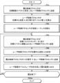
- Prior art date
- Legal status (The legal status is an assumption and is not a legal conclusion. Google has not performed a legal analysis and makes no representation as to the accuracy of the status listed.)
- Ceased
Links
Images












Classifications
-
- G—PHYSICS
- G03—PHOTOGRAPHY; CINEMATOGRAPHY; ANALOGOUS TECHNIQUES USING WAVES OTHER THAN OPTICAL WAVES; ELECTROGRAPHY; HOLOGRAPHY
- G03F—PHOTOMECHANICAL PRODUCTION OF TEXTURED OR PATTERNED SURFACES, e.g. FOR PRINTING, FOR PROCESSING OF SEMICONDUCTOR DEVICES; MATERIALS THEREFOR; ORIGINALS THEREFOR; APPARATUS SPECIALLY ADAPTED THEREFOR
- G03F7/00—Photomechanical, e.g. photolithographic, production of textured or patterned surfaces, e.g. printing surfaces; Materials therefor, e.g. comprising photoresists; Apparatus specially adapted therefor
- G03F7/70—Microphotolithographic exposure; Apparatus therefor
- G03F7/70483—Information management; Active and passive control; Testing; Wafer monitoring, e.g. pattern monitoring
- G03F7/70491—Information management, e.g. software; Active and passive control, e.g. details of controlling exposure processes or exposure tool monitoring processes
- G03F7/70525—Controlling normal operating mode, e.g. matching different apparatus, remote control or prediction of failure
-
- G—PHYSICS
- G03—PHOTOGRAPHY; CINEMATOGRAPHY; ANALOGOUS TECHNIQUES USING WAVES OTHER THAN OPTICAL WAVES; ELECTROGRAPHY; HOLOGRAPHY
- G03F—PHOTOMECHANICAL PRODUCTION OF TEXTURED OR PATTERNED SURFACES, e.g. FOR PRINTING, FOR PROCESSING OF SEMICONDUCTOR DEVICES; MATERIALS THEREFOR; ORIGINALS THEREFOR; APPARATUS SPECIALLY ADAPTED THEREFOR
- G03F7/00—Photomechanical, e.g. photolithographic, production of textured or patterned surfaces, e.g. printing surfaces; Materials therefor, e.g. comprising photoresists; Apparatus specially adapted therefor
- G03F7/20—Exposure; Apparatus therefor
-
- G—PHYSICS
- G03—PHOTOGRAPHY; CINEMATOGRAPHY; ANALOGOUS TECHNIQUES USING WAVES OTHER THAN OPTICAL WAVES; ELECTROGRAPHY; HOLOGRAPHY
- G03F—PHOTOMECHANICAL PRODUCTION OF TEXTURED OR PATTERNED SURFACES, e.g. FOR PRINTING, FOR PROCESSING OF SEMICONDUCTOR DEVICES; MATERIALS THEREFOR; ORIGINALS THEREFOR; APPARATUS SPECIALLY ADAPTED THEREFOR
- G03F7/00—Photomechanical, e.g. photolithographic, production of textured or patterned surfaces, e.g. printing surfaces; Materials therefor, e.g. comprising photoresists; Apparatus specially adapted therefor
- G03F7/70—Microphotolithographic exposure; Apparatus therefor
- G03F7/70008—Production of exposure light, i.e. light sources
- G03F7/70025—Production of exposure light, i.e. light sources by lasers
-
- G—PHYSICS
- G03—PHOTOGRAPHY; CINEMATOGRAPHY; ANALOGOUS TECHNIQUES USING WAVES OTHER THAN OPTICAL WAVES; ELECTROGRAPHY; HOLOGRAPHY
- G03F—PHOTOMECHANICAL PRODUCTION OF TEXTURED OR PATTERNED SURFACES, e.g. FOR PRINTING, FOR PROCESSING OF SEMICONDUCTOR DEVICES; MATERIALS THEREFOR; ORIGINALS THEREFOR; APPARATUS SPECIALLY ADAPTED THEREFOR
- G03F7/00—Photomechanical, e.g. photolithographic, production of textured or patterned surfaces, e.g. printing surfaces; Materials therefor, e.g. comprising photoresists; Apparatus specially adapted therefor
- G03F7/70—Microphotolithographic exposure; Apparatus therefor
- G03F7/70008—Production of exposure light, i.e. light sources
- G03F7/70041—Production of exposure light, i.e. light sources by pulsed sources, e.g. multiplexing, pulse duration, interval control or intensity control
-
- G—PHYSICS
- G03—PHOTOGRAPHY; CINEMATOGRAPHY; ANALOGOUS TECHNIQUES USING WAVES OTHER THAN OPTICAL WAVES; ELECTROGRAPHY; HOLOGRAPHY
- G03F—PHOTOMECHANICAL PRODUCTION OF TEXTURED OR PATTERNED SURFACES, e.g. FOR PRINTING, FOR PROCESSING OF SEMICONDUCTOR DEVICES; MATERIALS THEREFOR; ORIGINALS THEREFOR; APPARATUS SPECIALLY ADAPTED THEREFOR
- G03F7/00—Photomechanical, e.g. photolithographic, production of textured or patterned surfaces, e.g. printing surfaces; Materials therefor, e.g. comprising photoresists; Apparatus specially adapted therefor
- G03F7/70—Microphotolithographic exposure; Apparatus therefor
- G03F7/70483—Information management; Active and passive control; Testing; Wafer monitoring, e.g. pattern monitoring
- G03F7/7055—Exposure light control in all parts of the microlithographic apparatus, e.g. pulse length control or light interruption
- G03F7/70575—Wavelength control, e.g. control of bandwidth, multiple wavelength, selection of wavelength or matching of optical components to wavelength
-
- H—ELECTRICITY
- H01—ELECTRIC ELEMENTS
- H01S—DEVICES USING THE PROCESS OF LIGHT AMPLIFICATION BY STIMULATED EMISSION OF RADIATION [LASER] TO AMPLIFY OR GENERATE LIGHT; DEVICES USING STIMULATED EMISSION OF ELECTROMAGNETIC RADIATION IN WAVE RANGES OTHER THAN OPTICAL
- H01S5/00—Semiconductor lasers
- H01S5/06—Arrangements for controlling the laser output parameters, e.g. by operating on the active medium
- H01S5/062—Arrangements for controlling the laser output parameters, e.g. by operating on the active medium by varying the potential of the electrodes
- H01S5/06233—Controlling other output parameters than intensity or frequency
Definitions
- the present disclosure relates to an electronic device manufacturing method, a laser device, and a wavelength sequence calculation system.
- a KrF excimer laser device that outputs laser light with a wavelength of about 248 nm and an ArF excimer laser device that outputs laser light with a wavelength of about 193 nm are used.
- the spectral line width of the spontaneous oscillation light of the KrF excimer laser device and the ArF excimer laser device is as wide as 350-400 pm. Therefore, if the projection lens is made of a material that transmits ultraviolet light, such as KrF and ArF laser light, chromatic aberration may occur. As a result, resolution can be reduced. Therefore, it is necessary to narrow the spectral line width of the laser light output from the gas laser device to such an extent that the chromatic aberration can be ignored. Therefore, in the laser resonator of the gas laser device, a line narrowing module (LNM) including a band narrowing element (etalon, grating, etc.) is provided in order to narrow the spectral line width.
- LNM line narrowing module
- a gas laser device whose spectral line width is narrowed will be referred to as a band-narrowed laser device.
- an electronic device manufacturing method includes a pulse spectral shape of a pulsed laser beam and a pulsed laser beam of a plurality of pulses generated based on a wavelength sequence that periodically changes the central wavelength of the pulsed laser beam.
- a target integrated spectral shape to be realized by light a plurality of target central wavelengths assigned to a plurality of pulses to achieve the target integrated spectral shape, and the number of pulses assigned to each of the target central wavelengths, which are wavelengths and the number of assigned pulses per cycle of the sequence, and each of at least one first center wavelength with an assigned number of pulses of 2 or more among the target center wavelengths, the smaller the number of assigned pulses, the more time it takes for each other.
- calculating a wavelength sequence by assigning increasing intervals and then assigning each of at least one second center wavelength having an assigned pulse number of 1 among the target center wavelengths, and generating pulses based on the wavelength sequence; It involves generating laser light by a laser device, outputting the pulsed laser light to an exposure device, and exposing the pulsed laser light onto a photosensitive substrate in the exposure device to manufacture an electronic device.
- a laser device in another aspect of the present disclosure, includes a laser oscillator capable of changing the central wavelength of pulsed laser light, and a laser amplifier capable of amplifying and outputting pulse energy of the pulsed laser light output from the laser oscillator. , a processor; The processor determines a pulse spectral shape of the pulsed laser light and a target integrated spectral shape to be achieved by a plurality of pulses of the pulsed laser light generated based on a wavelength sequence that periodically changes the center wavelength of the pulsed laser light.
- a wavelength sequence is calculated by allocating each of the at least one second center wavelength having one allocated pulse number among the wavelengths, and the laser oscillator is controlled based on the wavelength sequence.
- a wavelength sequence calculation system includes a non-transitory computer-readable storage medium storing a wavelength sequence calculation program, and a CPU.
- the CPU executes a wavelength sequence calculation program to generate a plurality of pulses of pulsed laser light based on a wavelength sequence that periodically changes the pulse spectrum shape of the pulsed laser light and the central wavelength of the pulsed laser light.
- a process of calculating a wavelength sequence is performed by allocating increasing numbers and then allocating each of at least one second center wavelength having an allocation pulse number of 1 among the target center wavelengths.
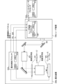
- FIG. 1 schematically shows the configuration of a lithography system in a comparative example.
- FIG. 2 schematically shows the configuration of a laser device in a comparative example.
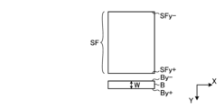
- FIG. 3 is a diagram for explaining how the position of the scan field changes with respect to the position of the beam cross section of the pulsed laser light in the exposure apparatus.
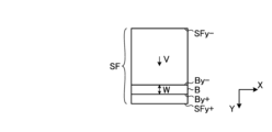
- FIG. 4 is a diagram for explaining how the position of the scan field changes with respect to the position of the beam cross section of the pulsed laser light in the exposure apparatus.
- FIG. 5 is a diagram for explaining how the position of the scan field changes with respect to the position of the beam cross section of the pulsed laser light in the exposure apparatus.
- FIG. 6 shows an example of a wavelength sequence for multi-wavelength oscillation.
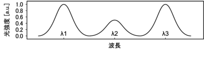
- FIG. 7 shows the integrated spectral shape sought by the wavelength sequence shown in FIG.
- FIG. 8 shows the target center wavelength set based on the wavelength sequence shown in FIG. 6 in chronological order.
- FIG. 9 shows the breakdown of the target center wavelength of the pulsed laser light of the number of N slit pulses irradiated over the required time T.
- FIG. 10 schematically shows the configuration of the lithography system in the first embodiment.
- FIG. 11 schematically shows the configuration of the laser device in the first embodiment.
- FIG. 12 schematically shows the configuration of the semiconductor laser in the first embodiment.
- FIG. 13 is a flow chart showing the procedure for calculating the wavelength sequence based on the target integrated spectrum shape in the first embodiment.
- FIG. 13 is a flow chart showing the procedure for calculating the wavelength sequence based on the target integrated spectrum shape in the first embodiment.
- FIG. 14 is a flow chart showing details of the process by which the laser control processor sends the pulse spectral shape to the exposure control processor.
- FIG. 15 is a flow chart showing the details of the process by which the exposure control processor calculates the target center wavelength and the number of assigned pulses.
- FIG. 16 shows an example of a target integrated spectrum shape.
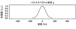
- FIG. 17 shows examples of pulse spectral shapes.
- FIG. 18 shows the results of rounding off values of 1 or more, with values less than 1 included in the function pm being 0.
- FIG. FIG. 19 is a flow chart showing a modification of the process of calculating the target center wavelength and the number of assigned pulses by the exposure control processor.
- FIG. 20 is a flow chart showing the details of the process of calculating the wavelength sequence by the exposure control processor.
- FIG. 20 is a flow chart showing the details of the process of calculating the wavelength sequence by the exposure control processor.
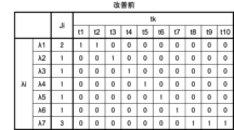
- FIG. 21 shows the wavelength sequence before improvement calculated without applying the processes of S32 to S34 of FIG.
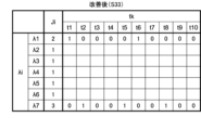
- FIG. 22 shows a state in which target center wavelengths with an assigned pulse number of 2 or more are assigned to several pulses included in the wavelength sequence in S33 of FIG.
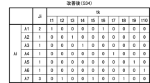
- FIG. 23 shows the improved wavelength sequence in which the target center wavelength with the number of assigned pulses of 1 is assigned to the remaining pulses included in the wavelength sequence in S34 of FIG.
- FIG. 24 superimposes ten integrated spectral shapes obtained according to the unimproved wavelength sequence shown in FIG.
- FIG. 25 shows overlaid ten integrated spectral shapes obtained according to the improved wavelength sequence shown in FIG.
- FIG. 26 schematically shows the configuration of the lithography system in the second embodiment.
- FIG. 27 is a flow chart showing the procedure for calculating the wavelength sequence based on the target integrated spectrum shape in the second embodiment.
- FIG. 28 schematically shows the configuration of the lithography system in the third embodiment.
- FIG. 29 is a flow chart showing the procedure for calculating the wavelength sequence based on the target integrated spectrum shape in the third embodiment.
- FIG. 1 schematically shows the configuration of a lithography system in a comparative example.
- the comparative examples of the present disclosure are forms known by the applicant to be known only by the applicant, and not known examples to which the applicant admits.
- a lithography system includes a laser apparatus 100 and an exposure apparatus 200 .
- a laser device 100 is shown in simplified form in FIG.
- the laser device 100 includes a laser control processor 130 .
- the laser control processor 130 is a processing device that includes a memory 132 storing a control program and a CPU (central processing unit) 131 that executes the control program.
- Memory 132 includes non-transitory computer-readable storage media.
- Laser control processor 130 is specially configured or programmed to perform the various processes contained in this disclosure.
- the laser device 100 is configured to generate a pulsed laser beam B ⁇ b>2 and output it toward the exposure device 200 .
- the exposure apparatus 200 includes an illumination optical system 201, a projection optical system 202, and an exposure control processor 210.
- FIG. 1 the exposure apparatus 200 includes an illumination optical system 201, a projection optical system 202, and an exposure control processor 210.
- the illumination optical system 201 illuminates a reticle pattern of a reticle (not shown) arranged on the reticle stage RT with the pulsed laser beam B2 incident from the laser device 100 .
- the projection optical system 202 reduces and projects the pulsed laser beam B2 transmitted through the reticle to form an image on a workpiece (not shown) placed on the workpiece table WT.
- the workpiece is a photosensitive substrate such as a semiconductor wafer coated with a resist film.
- the exposure control processor 210 is a processing device that includes a memory 212 storing control programs and a CPU 211 that executes the control programs.
- Memory 212 includes non-transitory computer-readable storage media.
- Exposure control processor 210 is specially configured or programmed to perform the various processes contained in this disclosure.
- the exposure control processor 210 supervises the control of the exposure apparatus 200 .
- Exposure control processor 210 sends various parameters including target center wavelength ⁇ t, target pulse energy Et, and target spectral linewidth ⁇ t, and trigger signal Tr to laser control processor 130 .
- Laser control processor 130 controls laser device 100 according to these parameters and signals.
- the exposure control processor 210 synchronously translates the reticle stage RT and the workpiece table WT in opposite directions. As a result, the workpiece is exposed to the pulsed laser beam B2 reflecting the reticle pattern. A reticle pattern is transferred to the semiconductor wafer by such an exposure process. After that, an electronic device can be manufactured through a plurality of steps.
- FIG. 2 schematically shows the configuration of a laser device 100 in a comparative example.
- FIG. 2 shows the exposure apparatus 200 in a simplified manner.
- Laser device 100 includes laser oscillator MO1, laser amplifier PO, and monitor module 17 in addition to laser control processor .
- Laser oscillator MO1 and laser amplifier PO each include an excimer laser.
- Laser oscillator MO1 is a master oscillator including laser chamber 10, power supply 12, band narrowing module 14, and spectral linewidth adjuster 15a.
- the band narrowing module 14 and the spectral linewidth adjuster 15a constitute a first optical resonator.
- a laser chamber 10 is arranged in the optical path of the first optical resonator.
- a laser chamber 10 is provided with windows 10a and 10b.
- the laser chamber 10 internally includes a pair of discharge electrodes 11a and 11b.
- the laser chamber 10 is filled with a laser gas containing, for example, argon gas or krypton gas as a rare gas, fluorine gas as a halogen gas, and neon gas as a buffer gas.
- the power supply device 12 is connected to the discharge electrode 11a.
- the discharge electrode 11b is connected to ground potential.
- the band narrowing module 14 includes a prism 14a, a grating 14b, and a rotating stage 14c.
- the prism 14a is arranged in the optical path of the light beam emitted from the window 10a.
- the prism 14a is arranged so that the surface of the prism 14a through which the light beam enters and exits is parallel to the discharge direction between the discharge electrodes 11a and 11b.
- Rotation stage 14 c includes a driver (not shown) connected to laser control processor 130 .
- the prism 14a is rotatable around an axis parallel to the discharge direction by a rotating stage 14c.
- the grating 14b is arranged in the optical path of the light beam that has passed through the prism 14a.
- the groove direction of the grating 14b is parallel to the discharge direction.
- the spectral linewidth adjuster 15a includes a cylindrical plano-convex lens 15b, a cylindrical plano-concave lens 15c, and a linear stage 15d.
- a cylindrical plano-concave lens 15c is positioned between the laser chamber 10 and the cylindrical plano-convex lens 15b.
- Linear stage 15 d includes a driver (not shown) connected to laser control processor 130 .
- the cylindrical plano-convex lens 15b and the cylindrical plano-concave lens 15c are arranged so that the convex surface of the cylindrical plano-convex lens 15b faces the concave surface of the cylindrical plano-concave lens 15c.
- the convex surface of the cylindrical plano-convex lens 15b and the concave surface of the cylindrical plano-concave lens 15c each have a focal axis parallel to the discharge direction.
- a flat surface located on the opposite side of the convex surface of the cylindrical plano-convex lens 15b is coated with a partially reflective film.
- a laser amplifier PO is arranged in the optical path of the pulsed laser beam B1 output from the spectral linewidth adjuster 15a.
- Laser amplifier PO is a power oscillator that includes laser chamber 20 , power supply 22 , rear mirror 24 and output coupling mirror 25 .
- the rear mirror 24 and the output coupling mirror 25 constitute a second optical resonator.
- Each of the rear mirror 24 and the output coupling mirror 25 is composed of a partially reflective mirror.
- Rear mirror 24 has a higher reflectivity than output coupling mirror 25 .
- a laser chamber 20 is arranged in the optical path of the second optical resonator.
- the laser chamber 20 is provided with windows 20a and 20b.
- the laser chamber 20 internally includes a pair of discharge electrodes 21a and 21b.
- the laser gas enclosed in the laser chamber 20 is the same as that enclosed in the laser chamber 10 .
- the power supply device 22 is connected to the discharge electrode 21a.
- the discharge electrode 21b is connected to ground potential.
- the monitor module 17 includes a beam splitter 17a and a beam monitor 17b.
- the beam splitter 17a is arranged in the optical path of the pulsed laser beam B2 outputted from the output coupling mirror 25.
- the beam monitor 17b is arranged in the optical path of the pulsed laser beam B2 reflected by the beam splitter 17a.
- a pulsed laser beam B ⁇ b>2 transmitted through the beam splitter 17 a is output to the exposure device 200 .
- the laser control processor 130 sends a control signal to the band narrowing module 14 based on the target center wavelength ⁇ t received from the exposure control processor 210 .
- the laser control processor 130 sends a control signal to the spectral linewidth adjuster 15a based on the target spectral linewidth ⁇ t received from the exposure control processor 210 .
- the laser control processor 130 sets voltage command values for the power supply devices 12 and 22 of the laser oscillator MO1 and the laser amplifier PO, respectively.
- the laser control processor 130 transmits an oscillation trigger signal based on the trigger signal Tr received from the exposure control processor 210 to the power supply devices 12 and 22 .
- the power supply device 12 of the laser oscillator MO1 When the power supply device 12 of the laser oscillator MO1 receives the oscillation trigger signal from the laser control processor 130, it applies a pulse-like high voltage according to the voltage command value between the discharge electrodes 11a and 11b. When a high voltage is applied between the discharge electrodes 11a and 11b, discharge occurs in the discharge space between the discharge electrodes 11a and 11b. The energy of this discharge excites the laser gas in the laser chamber 10 to shift to a high energy level. When the excited laser gas then shifts to a lower energy level, it emits light with a wavelength corresponding to the energy level difference.
- the light generated within the laser chamber 10 is emitted outside the laser chamber 10 through the windows 10a and 10b.
- Light emitted from the window 10 a enters the band narrowing module 14 .
- the light incident on the band narrowing module 14 has its beam width expanded by the prism 14a and enters the grating 14b.
- the light incident on the grating 14b is reflected by the plurality of grooves of the grating 14b and diffracted in directions corresponding to the wavelength of the light.
- Prism 14a reduces the beam width of the diffracted light from grating 14b and returns the light to laser chamber 10 through window 10a. As a result, of the light incident on the band narrowing module 14 , light near the desired wavelength is returned to the laser chamber 10 .
- the spectral linewidth adjuster 15a transmits part of the light emitted from the window 10b and outputs it as pulsed laser light B1, and reflects the other part and returns it to the laser chamber 10.
- the light emitted from the laser chamber 10 reciprocates between the band narrowing module 14 and the spectral linewidth adjuster 15a.
- This light is amplified each time it passes through the discharge space within the laser chamber 10 . Further, this light is band-narrowed each time it is folded back by the band-narrowing module 14, and becomes light having a steep wavelength distribution with a part of the range of wavelengths selected by the band-narrowing module 14 as the center wavelength.
- the laser-oscillated and narrow-band light is output from the spectral line width adjuster 15a as the pulsed laser light B1.
- the laser control processor 130 controls the rotary stage 14c included in the band narrowing module 14 via a driver (not shown).
- the angle of incidence of the light beam incident on the grating 14b changes according to the rotation angle of the rotary stage 14c, and the wavelength selected by the band narrowing module 14 changes.
- the laser control processor 130 controls the linear stage 15d included in the spectral linewidth adjuster 15a via a driver (not shown).
- the wavefront of light traveling from the spectral line width adjuster 15a to the band narrowing module 14 changes according to the distance between the cylindrical plano-convex lens 15b and the cylindrical plano-concave lens 15c.
- the spectral line width of the pulsed laser beam B1 changes as the wavefront changes.
- the pulsed laser beam B1 output from the spectral linewidth adjuster 15a is guided to the rear mirror 24 of the laser amplifier PO.
- the power supply device 22 of the laser amplifier PO When the power supply device 22 of the laser amplifier PO receives the oscillation trigger signal from the laser control processor 130, it applies a pulse-like high voltage according to the voltage command value between the discharge electrodes 21a and 21b. In response to the oscillation trigger signal to the laser oscillator MO1, the timing of the discharge between the discharge electrodes 21a and 21b is synchronized with the timing of the pulsed laser beam B1 entering the laser chamber 20 via the rear mirror 24 and the window 20a. A delay time of the oscillation trigger signal to the laser amplifier PO is set.
- the pulsed laser beam B1 incident on the laser chamber 20 reciprocates between the rear mirror 24 and the output coupling mirror 25, and the pulse energy is amplified every time it passes through the discharge space between the discharge electrodes 21a and 21b.
- the amplified light is output as pulsed laser light B2 from the output coupling mirror 25 of the laser amplifier PO.
- the beam monitor 17b measures the wavelength of the pulsed laser beam B2 and transmits the measured wavelength to the laser control processor .
- the laser control processor 130 feedback-controls the rotary stage 14c based on the target center wavelength ⁇ t received from the exposure control processor 210 and the measured wavelength. Further, the laser control processor 130 controls the rotary stage 14c even when the target center wavelength ⁇ t changes for each pulse, so that the pulsed laser beam B1 output from the laser oscillator MO1 and the pulsed laser beam output from the laser amplifier PO The central wavelength of light B2 can be changed for each pulse.
- the beam monitor 17b measures the spectral linewidth of the pulsed laser beam B2 and transmits the measured spectral linewidth to the laser control processor .
- the laser control processor 130 feedback-controls the linear stage 15d based on the target spectral linewidth ⁇ t received from the exposure control processor 210 and the measured spectral linewidth.
- the beam monitor 17b measures the pulse energy of the pulsed laser beam B2 and transmits the measured pulse energy to the laser control processor .
- the laser control processor 130 feedback-controls the voltage command values set in the power supply devices 12 and 22 based on the target pulse energy Et received from the exposure control processor 210 and the measured pulse energy.
- the pulsed laser beam B ⁇ b>2 transmitted through the beam splitter 17 a enters the exposure device 200 .
- FIGS. 3 to 5 show how the position of the scan field SF changes with respect to the position of the beam cross section B of the pulse laser beam B2 in the exposure apparatus 200.
- FIG. The scan field SF corresponds to, for example, a region where some semiconductor chips out of many semiconductor chips formed on the work piece are formed.
- a resist film is applied to the scan field SF.
- the moving direction of the scan field SF is defined as the Y-axis direction, and the direction perpendicular to the Y-axis direction within the plane of the scan field SF is defined as the X-axis direction.
- the width of the scan field SF in the X-axis direction is the same as the width in the X-axis direction of the beam cross-section B of the pulsed laser beam B2 at the workpiece position.
- the width of the scan field SF in the Y-axis direction is larger than the width W in the Y-axis direction of the beam cross section B of the pulsed laser beam B2 at the workpiece position.
- FIG. 3 The procedure for exposing the scan field SF with the pulsed laser beam B2 is performed in the order of FIGS. 3, 4, and 5.
- FIG. 3 the workpiece is positioned so that the +Y direction end SFy+ of the scan field SF is located at a predetermined distance in the ⁇ Y direction from the position of the ⁇ Y direction end By ⁇ of the beam cross section B.
- a table WT is positioned.
- the workpiece table WT is accelerated in the +Y direction.
- the velocity of the workpiece table WT reaches V by the time the +Y-direction end SFy+ of the scan field SF coincides with the position of the -Y-direction end By- of the beam cross-section B.
- FIG. As shown in FIG.
- the scan field SF is exposed while the work piece table WT is moved so that the position of the scan field SF performs uniform linear motion at a velocity V with respect to the position of the beam cross section B.
- the scan field SF is exposed. finish. In this manner, exposure is performed while the scan field SF moves with respect to the position of the beam cross section B.
- F is the repetition frequency of the pulsed laser beam B2.
- FIG. 6 shows an example of a wavelength sequence for multi-wavelength oscillation.
- Each of t1 to t5 indicates the output timing of one pulse of the pulsed laser beam B2, and t1, t2, t3, t4, t5, t1, t2, t3, . . . t1 to t5 are repeated in this order.
- the number of pulses corresponding to one period of the wavelength sequence is the number of pulses per period Kmax, and each integer from 1 to Kmax is k
- the number of pulses per period Kmax is 5 in FIG. can be collectively denoted by tk.
- Each of ⁇ 1 to ⁇ 3 indicates the target center wavelength of one pulse of the pulsed laser light B2 assigned to each of the pulses included in the wavelength sequence, and the wavelength increases in the order of ⁇ 1, ⁇ 2, and ⁇ 3.
- Imax be the number of target center wavelengths included in the wavelength sequence, and i be an individual integer from 1 to Imax, Imax is 3 in FIG. can.
- the wavelength sequence includes columns specifying output timings t1 to t5, respectively, and rows specifying target center wavelengths ⁇ 1 to ⁇ 3, respectively. "1” or “0” is entered in the fields identified by these columns and rows. "1” indicates that the pulsed laser beam B2 of the target center wavelength corresponding to the row is output at the output timing corresponding to the column.
- One target center wavelength is set for each of the output timings t1 to t5, and only one "1” is entered in the column specified for each of the output timings t1 to t5. Columns other than "1" are filled with "0".
- the wavelength sequence in FIG. 6 has output timings t1, t2, t3, t4, t5, t1, t2, t3, . . . , ⁇ 1, ⁇ 1, ⁇ 2, ⁇ 3, ⁇ 3, ⁇ 1, ⁇ 1, ⁇ 2, . . . It defines that the center wavelength of the pulsed laser beam B2 is changed periodically by setting as follows.
- FIG. 7 shows the integrated spectral shape to be obtained by the wavelength sequence shown in FIG.
- the integrated spectrum shape is obtained by irradiating one point with the pulsed laser beam B2 having the number of N slit pulses of Ns while periodically changing the target central wavelength of the pulsed laser beam B2, so that the pulse spectrum shape of each pulse can be changed to N It refers to the spectrum shape obtained by integrating over the number of slit pulses Ns.
- FIG. 7 shows an integrated spectrum shape having three peaks at target center wavelengths ⁇ 1 to ⁇ 3, and peak intensities at target center wavelengths ⁇ 1 and ⁇ 3 being higher than peak intensity at target center wavelength ⁇ 2.
- the number of pulses whose target center wavelength is ⁇ 2.
- the focal length of the exposure apparatus 200 depends on the wavelength of the pulsed laser beam B2.
- the multi-wavelength pulsed laser beam B2 incident on the exposure apparatus 200 can be imaged at a plurality of different positions in the direction of the optical path axis of the pulsed laser beam B2, so that the depth of focus can be substantially increased. can. For example, even when a resist film having a large thickness is exposed, the imaging performance in the thickness direction of the resist film can be maintained.
- the cross-sectional shape of the developed resist film can be controlled.
- FIG. 8 shows the target center wavelengths ⁇ 1 to ⁇ 3 set based on the wavelength sequence shown in FIG. 6 in time series.
- the breakdown of the target central wavelength included in the pulsed laser beam B2 with the N-slit pulse number Ns that is irradiated over the required time T from the output timing t1 is within the range of the arrow indicating the period of the required time T starting from the output timing t1. It is obtained by counting the target center wavelengths ⁇ 1, ⁇ 2, and ⁇ 3.
- the pulsed laser beam B2 irradiated from the output timing t1 for the required time T includes five pulses with a target center wavelength of ⁇ 1, two pulses with a target center wavelength of ⁇ 2, and a pulse with a target center wavelength of ⁇ 3. contains four.
- FIG. 9 shows the breakdown of the target center wavelength of the pulsed laser beam B2 with the N slit pulse number Ns that is irradiated over the required time T.
- the N-slit pulse number Ns is constant at 11 even when the required time T starts from any of the output timings t1 to t5.
- the breakdown of the target center wavelength fluctuates.
- exposure of the scan field SF is performed while the scan field SF is moved with respect to the position of the beam cross section B. Therefore, depending on the position within the scan field SF, the integrated spectrum shape is will be different.
- the N-slit pulse number Ns As a method of keeping the integrated spectrum shape constant without varying it, it is conceivable to set the N-slit pulse number Ns to a multiple of the pulse number Kmax within a period corresponding to one period of the wavelength sequence.
- one of the repetition frequency F of the pulse laser beam B2 the speed V at which the scan field SF is moved, and the width W of the beam cross section B of the pulse laser beam B2 must be changed. and must be controlled accurately.
- the intra-cycle pulse number Kmax to be a divisor of the N slit pulse number Ns.
- the range of selection of the per-cycle pulse number Kmax is narrowed, it may become difficult to calculate a wavelength sequence for obtaining a desired integrated spectrum shape.
- FIG. 10 schematically shows the configuration of the lithography system in the first embodiment.
- the laser control processor 130 included in the laser device 100a transmits the pulse spectral shape g of the pulsed laser beam B2 to the exposure control processor 210 included in the exposure device 200a.
- the exposure control processor 210 calculates the wavelength sequence and transmits the target center wavelength ⁇ i based on the wavelength sequence to the laser control processor 130 for each pulse.
- the exposure control processor 210 in the first embodiment corresponds to the wavelength sequence calculation system in this disclosure.
- the exposure control processor 210 may be connected to a server computer processor 310 outside the exposure apparatus 200a.
- the server computer processor 310 is a processing device including a memory 312 storing a control program and a CPU 311 executing the control program. Memory 312 includes non-transitory computer-readable storage media.
- Server computer processor 310 is specially configured or programmed to perform the various processes involved in this disclosure.
- the server computer processor 310 instead of the exposure control processor 210 may perform the processes (S2 and S3) for calculating the target center wavelength ⁇ i, the number of assigned pulses Ji, and the wavelength sequence.
- the server computer processor 310 corresponds to the wavelength sequence calculation system in this disclosure.
- the combination of these processors corresponds to the wavelength sequence calculation system in the present disclosure.
- FIG. 11 schematically shows the configuration of a laser device 100a according to the first embodiment.
- Laser device 100 a includes laser oscillator MO 2 , laser amplifier PA, monitor module 17 , shutter 19 and laser control processor 130 .
- Laser oscillator MO2 contains a solid-state laser and laser amplifier PA contains an excimer laser.
- the laser device in the present disclosure is not limited to the laser device 100a shown in FIG. 11, and the laser device 100 shown in FIG. 2 may be used.
- the laser oscillator MO2 includes a semiconductor laser 60, a titanium sapphire amplifier 71, a wavelength conversion system 72, a pumping laser 73, and a solid state laser control processor 13.
- the semiconductor laser 60 is a laser system including a distributed feedback semiconductor laser DFB and a semiconductor optical amplifier SOA. Details of the semiconductor laser 60 will be described later with reference to FIG.
- Titanium-sapphire amplifier 71 is an amplifier containing a titanium-sapphire crystal.
- the pumping laser 73 is a laser device that outputs the second harmonic of a YLF (yttrium lithium fluoride) laser to excite the titanium sapphire crystal of the titanium sapphire amplifier 71 .
- YLF yttrium lithium fluoride
- the wavelength conversion system 72 is a system that includes an LBO (lithium triborate) crystal and a KBBF (potassium beryllium fluoroborate) crystal, and outputs the fourth harmonic of the incident light as a pulsed laser beam B1.
- LBO lithium triborate
- KBBF potassium beryllium fluoroborate
- the solid-state laser control processor 13 is a processing device including a memory 13b storing a control program and a CPU 13a executing the control program.
- Memory 13b includes a non-transitory computer-readable storage medium.
- Solid-state laser control processor 13 is specially configured or programmed to perform various processes contained in this disclosure.
- the solid-state laser control processor 13 is configured to be connected to and control the semiconductor laser 60, the wavelength conversion system 72, and the pumping laser 73, respectively.
- the laser amplifier PA includes a laser chamber 30, a power supply 32, a concave mirror 34, and a convex mirror 35.
- the configurations of the laser chamber 30 and the power supply 32 included in the laser amplifier PA are the same as those of the laser chamber 10 and the power supply 12 described with reference to FIG. 2, except that argon gas is used as the rare gas.
- the reference numerals of the windows included in the laser chamber 30 are changed to 30a and 30b, and the reference numerals of the discharge electrodes are changed to 31a and 31b.
- the convex mirror 35 is arranged on the optical path of the pulsed laser beam B1 output from the laser oscillator MO2 and passed through the laser chamber 30 .
- the concave mirror 34 is arranged in the optical path of the pulsed laser beam B1 that has been reflected by the convex mirror 35 and passed through the laser chamber 30 again.
- the configurations of the monitor module 17 and the laser control processor 130 are similar to the corresponding configurations in the laser device 100 described with reference to FIG.
- the shutter 19 is positioned on the optical path of the pulsed laser beam B2 that has passed through the monitor module 17 .
- the shutter 19 is configured to switch between passing and blocking the pulsed laser beam B2 to the exposure device 200a.
- the semiconductor laser 60 outputs a pulsed laser beam with a wavelength of approximately 773.6 nm, and the titanium-sapphire amplifier 71 amplifies and outputs this pulsed laser beam.
- the wavelength conversion system 72 converts the pulsed laser beam with a wavelength of approximately 773.6 nm into the pulsed laser beam B1 with a wavelength of approximately 193.4 nm and outputs the pulsed laser beam B1 toward the laser amplifier PA.
- the pulsed laser beam B1 incident on the laser amplifier PA passes through the discharge space in the laser chamber 30, is reflected by the convex mirror 35, and is given a beam divergence angle according to the curvature of the convex mirror 35. This pulsed laser beam B1 passes through the discharge space in the laser chamber 30 again.
- the pulsed laser beam B1 that has been reflected by the convex mirror 35 and passed through the laser chamber 30 is reflected by the concave mirror 34 and returned to substantially parallel light.
- This pulsed laser beam B1 passes through the discharge space in the laser chamber 30 once more, passes through the monitor module 17 as the pulsed laser beam B2, and is emitted to the outside of the laser device 100a.
- a high voltage is applied to the discharge electrodes 31a and 31b so that discharge starts in the discharge space inside the laser chamber 30 when the pulsed laser beam B1 is incident on the window 30a of the laser chamber 30 from the laser oscillator MO2.
- the pulse laser beam B1 has its beam width expanded by the convex mirror 35 and concave mirror 34, and its pulse energy is amplified while it passes through the discharge space three times.
- the amplified light is output as pulsed laser light B2 from the window 30b of the laser amplifier PA.
- FIG. 12 schematically shows the configuration of the semiconductor laser 60 in the first embodiment.
- the semiconductor laser 60 includes a distributed feedback semiconductor laser DFB and a semiconductor optical amplifier SOA.
- the distributed feedback semiconductor laser DFB includes a function generator 61 , a current controller 62 , a Peltier element 63 , a temperature controller 64 , a semiconductor laser element 65 and a temperature sensor 66 .
- the semiconductor laser element 65 is a laser element whose oscillation wavelength can be changed by temperature or current value.
- a current controller 62 is connected to the semiconductor laser element 65 .
- a Peltier element 63 and a temperature sensor 66 are fixed to the semiconductor laser element 65 .
- a temperature controller 64 is connected to the Peltier element 63 and the temperature sensor 66 .
- the current controller 62 corresponds to the wavelength tuner in the present disclosure.
- the semiconductor laser element 65 outputs CW (continuous wave) laser light with a wavelength of approximately 773.6 nm.
- the temperature controller 64 supplies current to the Peltier device 63 according to the set temperature output from the solid-state laser control processor 13 .
- the Peltier element 63 cools or heats the semiconductor laser element 65 by transferring thermal energy from one surface of the Peltier element 63 to the other according to the current supplied from the temperature control unit 64 . .
- a temperature sensor 66 detects the temperature of the semiconductor laser element 65 .
- the temperature controller 64 feedback-controls the current supplied to the Peltier element 63 based on the set temperature output from the solid-state laser control processor 13 and the temperature detected by the temperature sensor 66 . By controlling the semiconductor laser element 65 to the set temperature, the wavelength of the CW laser light output from the semiconductor laser element 65 can be maintained at a value around 773.6 nm.
- the function generator 61 generates an electrical signal having a periodic waveform according to the control signal output from the solid-state laser control processor 13.
- the current control section 62 periodically changes the current supplied to the semiconductor laser element 65 according to the waveform of the electrical signal generated by the function generator 61 .
- the wavelength of the CW laser light output from the semiconductor laser element 65 changes periodically.
- the semiconductor optical amplifier SOA amplifies the CW laser light output from the semiconductor laser element 65 into a pulsed shape and outputs the pulsed laser light toward the titanium-sapphire amplifier 71 .
- the current supplied to the semiconductor laser element 65 makes it possible to change the central wavelengths of the pulsed laser light B1 output from the laser oscillator MO2 and the pulsed laser light B2 output from the laser amplifier PA for each pulse.
- FIG. 13 is a flowchart showing a procedure for calculating a wavelength sequence based on the target integrated spectral shape s in the first embodiment. .
- the processing shown in FIG. 13 is mainly performed by the exposure control processor 210 included in the exposure device 200a, and part of the processing is performed by the laser control processor 130 included in the laser device 100a.
- the laser control processor 130 sends the pulse spectral shape g to the exposure control processor 210 .
- the pulse spectral shape g is the spectral shape of one pulse of the pulsed laser beam B2 output by the laser device 100a, and a specific example thereof will be described with reference to FIG. Details of the processing of S1 will be described with reference to FIG.
- the exposure control processor 210 calculates the target center wavelength ⁇ i and the assigned number of pulses Ji.
- the target center wavelength ⁇ i indicates the wavelength assigned to the multiple pulses included in the wavelength sequence to achieve the target integrated spectral shape s.
- the assigned number of pulses Ji is the number of pulses of each target center wavelength ⁇ i per cycle of the wavelength sequence. Details of the processing of S2 will be described with reference to FIGS. 15 to 18. FIG.
- the exposure control processor 210 calculates a wavelength sequence. Details of the processing of S3 will be described with reference to FIGS. 20 to 23. FIG.
- the exposure control processor 210 transmits the target center wavelength ⁇ i to the laser control processor 130 for each pulse based on the wavelength sequence.
- the exposure control processor 210 also sends the target pulse energy Et and the target spectral linewidth ⁇ t to the laser control processor 130 .
- the exposure control processor 210 sends the trigger signal Tr to the laser control processor 130 .
- the laser control processor 130 controls the laser device 100a to generate the pulsed laser beam B2 and output it to the exposure device 200a according to the target center wavelength ⁇ i, target pulse energy Et, target spectral linewidth ⁇ t, and trigger signal Tr. Control.
- the exposure control processor 210 determines whether or not exposure has ended. For example, when the exposure of one semiconductor wafer is completed and the target integrated spectral shape s is to be changed, it is determined that the exposure has been completed. If the exposure has not ended (S8: NO), the process returns to S4. If the exposure has ended (S8: YES), the processing of this flowchart ends.
- FIG. 14 is a flow chart showing the details of the process by which the laser control processor 130 transmits the pulse spectral shape g to the exposure control processor 210 .
- the processing shown in FIG. 14 corresponds to the subroutine of S1 in FIG.
- the laser control processor 130 receives the target spectral linewidth ⁇ t from the exposure control processor 210 .
- the target spectral linewidth ⁇ t received here is the target spectral linewidth of the pulsed laser beam B2 generated for measuring the pulse spectral shape g.
- the received target spectral linewidth ⁇ t is stored in memory 132 .
- the laser control processor 130 controls the laser device 100a to generate the pulsed laser beam B2 according to the target spectral linewidth ⁇ t. At this time, the shutter 19 may be closed.
- the laser control processor 130 measures the pulse spectral shape g of the pulsed laser beam B ⁇ b>2 with the monitor module 17 .
- the monitor module 17 in this case corresponds to the spectrum detector in this disclosure.
- the laser control processor 130 transmits the measured pulse spectral shape g to the exposure control processor 210 .
- the processing of this flowchart ends, and the processing returns to the processing shown in FIG.
- the laser control processor 130 reads from the memory 132 the data of the reference spectral shape and the target spectral linewidth ⁇ t that serve as the reference for the pulse spectral shape g, and transforms the reference spectral shape based on the target spectral linewidth ⁇ t.
- a pulse spectral shape g may be obtained.
- the reference spectral shape is, for example, a Gaussian spectral shape.
- the laser control processor 130 may acquire the pulse spectral shape g by reading out from the memory 132 spectral shape data of a pulsed laser beam output from a laser device other than the laser device 100a.
- Other laser devices are, for example, similar laser devices.
- an average of spectral shapes of pulsed laser beams output from a plurality of laser devices of the same type may be obtained as the pulse spectral shape g.
- the exposure control processor 210 may read the necessary data from the memory 212 to obtain the pulse spectral shape g. Further, when a monitor module (not shown) is provided inside the exposure apparatus 200a, the pulsed laser beam B2 may be output to the exposure apparatus 200a, and the pulse spectrum shape g may be measured by the monitor module inside the exposure apparatus 200a. good.
- FIG. 15 is a flow chart showing details of the processing by the exposure control processor 210 to calculate the target center wavelength ⁇ i and number of assigned pulses Ji.
- the processing shown in FIG. 15 corresponds to the subroutine of S2 in FIG.
- the exposure control processor 210 acquires the target integrated spectral shape s and the pulse spectral shape g.
- the target integrated spectral shape s may be one stored in memory 212 .
- FIG. 16 shows an example of the target integrated spectrum shape s
- FIG. 17 shows an example of the pulse spectrum shape g.
- the horizontal axis indicates the wavelength as the deviation when the reference wavelength is 0
- the vertical axis indicates the light intensity as the ratio when the peak value is 1.
- exposure control processor 210 calculates Fourier transforms S and G of target integrated spectral shape s and pulse spectral shape g, respectively, as follows.
- S F (s)
- G F (g)
- F(a) denotes the Fourier transform of function a.
- the exposure control processor 210 calculates the inverse Fourier transform p of S/G obtained by dividing the Fourier transform S by the Fourier transform G as follows.
- p F -1 (S/G)
- F ⁇ 1 (A) denotes the inverse Fourier transform of function A.
- S/G corresponds to the third function in this disclosure.
- the calculation of the Fourier transform and the inverse Fourier transform is preferably performed by the fast Fourier transform (FFT) and the inverse fast Fourier transform (IFFT).
- the inverse Fourier transform p contains values for each of the discrete wavelength components.
- the exposure control processor 210 obtains the minimum value pmin that is greater than or equal to the first threshold among the values included in the inverse Fourier transform p.
- the exposure control processor 210 integerizes the values contained in the function pm. Specifically, among the values included in the function pm, values less than 1 are set to 0, and values greater than or equal to 1 are rounded off to the nearest whole number. In S28, the exposure control processor 210 sets the wavelength corresponding to the value of 1 or more among the values included in the function pm as the target central wavelength ⁇ i, and sets the value obtained by rounding in S27 as the assigned pulse number Ji.
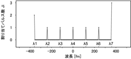
- FIG. 18 shows the result of rounding off values of 1 or more, with values less than 1 included in the function pm being 0.
- the horizontal axis indicates the wavelength as a deviation when the reference wavelength is 0, and the vertical axis indicates the assigned pulse number Ji obtained by integerizing the values contained in the function pm.
- the assigned pulse number J1 for the target central wavelength ⁇ 1 is 2
- the assigned pulse numbers J2 to J6 for the target central wavelengths ⁇ 2 to ⁇ 6 are all 1
- the assigned pulse number J7 for the target central wavelength ⁇ 7 is 3.
- the target center wavelength ⁇ i and the number of assigned pulses Ji are calculated.
- FIG. 19 is a flow chart showing a modified example of processing for the exposure control processor 210 to calculate the target center wavelength ⁇ i and the number of assigned pulses Ji.
- the process shown in FIG. 19 differs from the process shown in FIG. 15 in that S24a is added after S23 and S25a-S28a are performed instead of S25-S28.
- the exposure control processor 210 obtains a normalized inverse Fourier transform pn by normalizing the inverse Fourier transform p so that the maximum value is 1. Specifically, the value contained in the inverse Fourier transform p is divided by its maximum value.
- the normalized inverse Fourier transform pn corresponds to the fifth function in this disclosure.
- the exposure control processor 210 acquires the minimum value pnmin that is greater than or equal to the second threshold among the values included in the normalized inverse Fourier transform pn.
- the second threshold is preferably 0.1 or more and 0.2 or less.
- the exposure control processor 210 integerizes the values contained in the function pnm. Specifically, among the values included in the function pnm, values less than 1 are set to 0, and values greater than or equal to 1 are rounded off.
- the exposure control processor 210 sets the wavelength corresponding to the value of 1 or more among the values included in the function pnm as the target center wavelength ⁇ i, and sets the value obtained by rounding in S27a as the assigned pulse number Ji.
- the process of this flow chart ends and returns to the process shown in FIG. Otherwise, the process shown in FIG. 19 is similar to that in FIG.
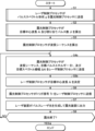
- FIG. 20 is a flow chart showing the details of the process of calculating the wavelength sequence by the exposure control processor 210 .
- the processing shown in FIG. 20 corresponds to the subroutine of S3 in FIG.
- the exposure control processor 210 sums up the assigned pulse numbers Ji for all the target center wavelengths ⁇ i to calculate the per-cycle pulse number Kmax corresponding to one period of the wavelength sequence.
- FIG. 21 shows the wavelength sequence before improvement calculated without applying the processes of S32 to S34 of FIG.
- a target center wavelength ⁇ i is assigned to Kmax, that is, a plurality of pulses output at 10 output timings tk.
- the correspondence relationship between the output timing tk and the target center wavelength ⁇ i is determined such that the larger the value of k, the larger the value of i.
- the allocation interval IVi indicates how many pulses of time are spaced apart from each other in the wavelength sequence to arrange the target center wavelength ⁇ i.
- the assignment interval IVi increases for the target center wavelength ⁇ i with the smaller assigned pulse number Ji.
- the exposure control processor 210 assigns the target center wavelength ⁇ i with the assigned pulse number Ji of 2 or more to several pulses included in the wavelength sequence.
- Each of the target center wavelengths ⁇ i for which the number of assigned pulses Ji is 2 or more corresponds to the first center wavelength in the present disclosure
- FIG. 22 shows a state in which the target center wavelengths ⁇ 1 and ⁇ 7 with the assigned pulse number Ji of 2 or more are assigned to several pulses included in the wavelength sequence in S33 of FIG. Specific allocation methods are as follows (a) to (c).
- the target center wavelength ⁇ i is assigned in ascending order of the number of assigned pulses Ji. That is, the target center wavelength ⁇ 1 is assigned first, and then the target center wavelength ⁇ 7 is assigned.
- the allocation interval IVi of the target center wavelength ⁇ i According to the allocation interval IVi of the target center wavelength ⁇ i. Therefore, the smaller the number of assigned pulses Ji is for the target center wavelength ⁇ i, the longer the time interval between the target center wavelengths ⁇ i. If the allocation interval IVi is not an integer, the allocation interval IVi is rounded or truncated to an integer after the decimal point. For example, a target center wavelength ⁇ 1 with an assigned pulse number J1 of 2 and an assigned interval IVi of 5 is assigned to pulses at output timings t1 and t6. In this way, by following the allocation interval IVi, the target center wavelength ⁇ 1 with the allocation pulse number J1 of 2 has a minimum time interval of 5 pulses in the wavelength sequence. value is maximum.
- the target center wavelength ⁇ 7 with the assigned pulse number J7 of 3 and the assigned interval IVi of 10/3 is not assigned to the output timings t1 and t6, but assigned to the pulses at the output timings t2, t5, and t8.
- the target center wavelength ⁇ 7 with the assigned number of pulses J7 of 3 has a minimum time interval of 3 pulses in the wavelength sequence, and in this allocation, the minimum time interval is the maximum.
- the exposure control processor 210 assigns the target center wavelength ⁇ i with the assigned pulse number Ji of 1 to the remaining pulses included in the wavelength sequence.
- Each of the target center wavelengths ⁇ i for which the number of assigned pulses Ji is 1 corresponds to the second center wavelength in the present disclosure.
- FIG. 23 shows the improved wavelength sequence in which the target central wavelengths ⁇ 2 to ⁇ 6 with the assigned pulse number Ji of 1 are assigned to the remaining pulses included in the wavelength sequence in S34 of FIG.
- the target center wavelengths ⁇ 2 to ⁇ 6 with the assigned pulse number Ji of 1 are not assigned to the pulse at the output timing tk to which the target center wavelength ⁇ i has already been assigned. That is, the target center wavelengths ⁇ 2 to ⁇ 6 with the assigned pulse number Ji of 1 are not assigned to the pulses at the output timings t1, t2, t5, t6, and t8, and are not assigned to the pulses at the output timings t3, t4, t7, t9, and t10. , are assigned so as not to overlap each other.
- the wavelength sequence is calculated as described above. After S34, the process of the flowchart of FIG. 20 ends and returns to the process shown in FIG.
- the exposure control processor 210 determines the pulse spectral shape g of the pulsed laser beam B2 and the target integrated spectral shape s to be realized by the pulsed laser beam B2 of a plurality of pulses. and get These multiple pulses are generated based on a wavelength sequence that periodically changes the central wavelength of the pulsed laser beam B2.
- the exposure control processor 210 also sets a plurality of target central wavelengths ⁇ i assigned to a plurality of pulses to achieve the target integrated spectral shape s, and the number of pulses Ji assigned to each of the target central wavelengths ⁇ i, which is one of the wavelength sequences. The number of assigned pulses Ji per period is calculated.
- the exposure control processor 210 sets each of at least one target center wavelengths ⁇ 1 and ⁇ 7 for which the assigned pulse number Ji of the target center wavelength ⁇ i is 2 or more, and the smaller the assigned pulse number Ji, the larger the time interval between each other. and then assigning each of at least one target center wavelength ⁇ 2 to ⁇ 6 having an assigned pulse number Ji of 1 among the target center wavelengths ⁇ i to calculate a wavelength sequence.
- the exposure control processor 210 sets the target central wavelength ⁇ i for each pulse based on the wavelength sequence, and transmits it to the laser device 100a.
- the laser device 100a generates a pulsed laser beam B2 and outputs it to the exposure device 200a.
- the exposure apparatus 200a exposes a workpiece within the exposure apparatus 200a to a pulsed laser beam B2 in order to manufacture an electronic device.
- the bias in the arrangement of the target center wavelengths ⁇ i in the wavelength sequence can be suppressed. Therefore, the breakdown of the target center wavelength ⁇ i of the pulsed laser beam B2 irradiated over the required time T is suppressed from fluctuating depending on which one of the plurality of output timings tk defined by the wavelength sequence starts the required time T. can be Therefore, variation in the shape of the integrated spectrum depending on the position within the scan field SF is suppressed.
- FIG. 24 shows ten accumulated spectral shapes obtained according to the wavelength sequence before improvement shown in FIG.
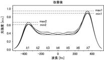
- FIG. 25 shows overlaid ten integrated spectral shapes obtained according to the improved wavelength sequence shown in FIG.
- the curves included in each of FIGS. 24 and 25 include ten curves, although some of the curves overlap each other.
- the horizontal axis indicates the wavelength as a deviation when the reference wavelength is 0, and the vertical axis indicates the light intensity as a ratio when the maximum value max1 described later in FIG. 24 is 1.
- the N slit pulse number Ns is set to 52.
- the highest peak is the first peak and the second highest peak is the second peak.
- the first peak is located near the target center wavelength ⁇ 7 and the second peak is located near the target center wavelength ⁇ 1.
- the maximum value of the first peak is max1 and the minimum value of the first peak is min1.
- the maximum value of the second peak is max2, and the minimum value of the second peak is min2.
- the amount of variation V1 of the first peak and the amount of variation V2 of the second peak evaluated by the following formulas were 12.8% and 19.2%, respectively.
- V1 (max1 ⁇ min1)/((max1+min1)/2) ⁇ 100
- V2 (max2-min2)/((max2+min2)/2) ⁇ 100
- the fluctuation amount V1 of the first peak and the fluctuation amount V2 of the second peak are improved to 6.4% and 9.6%, respectively, and it is found that the fluctuation of the integrated spectrum shape is suppressed. rice field.
- the exposure control processor 210 performs the inverse Fourier transform of S/G obtained by dividing the Fourier transform S of the target integrated spectral shape s by the Fourier transform G of the pulse spectral shape g. Based on p, the target center wavelength ⁇ i is calculated. According to this, the appropriate target center wavelength ⁇ i can be calculated by deconvolving the target integrated spectral shape s with the pulse spectral shape g.
- the exposure control processor 210 calculates the assigned pulse number Ji based on the inverse Fourier transform p. According to this, an appropriate assigned pulse number Ji can be calculated by deconvolution integral.
- the exposure control processor 210 divides the inverse Fourier transform p by the minimum value pmin that is greater than or equal to the first threshold among the plurality of values included in the inverse Fourier transform p.
- a center wavelength corresponding to one or more values among the values of the function pm thus obtained is calculated as the target center wavelength ⁇ i. According to this, the noise included in the inverse Fourier transform p can be removed, and the target center wavelength ⁇ i at which the assigned pulse number Ji is 1 or more can be calculated.
- the exposure control processor 210 divides the inverse Fourier transform p by the minimum value pmin that is greater than or equal to the first threshold among the plurality of values included in the inverse Fourier transform p. Integer the value of the function pm obtained by The exposure control processor 210 calculates the central wavelength corresponding to one or more integer values as the target central wavelength ⁇ i, and assigns the number of pulses Ji to each target central wavelength ⁇ i corresponding to the integer value. Calculate as According to this, the target central wavelength ⁇ i can be set for each pulse contained in the pulsed laser beam B2 by integerizing the value of the function pm.
- the exposure control processor 210 sets the values of the function pm that are less than 1 to 0, and rounds off the values of 1 or more to integerize the values of the function pm. . According to this, since all values less than 1 are discarded, the number of target center wavelengths ⁇ i can be suppressed, and lengthening of one period of the wavelength sequence can be suppressed.
- the exposure control processor 210 obtains the normalized inverse Fourier transform pn by normalizing the inverse Fourier transform p so that the maximum value is one.
- the exposure control processor 210 divides the function pnm obtained by dividing the inverse normalized Fourier transform pn by the minimum value pnmin that is equal to or greater than the second threshold among the plurality of values included in the inverse normalized Fourier transform pn.
- a central wavelength corresponding to one or more of the values is calculated as the target central wavelength ⁇ i. According to this, by normalizing the inverse Fourier transform p, the relationship between the normalized inverse Fourier transform pn and the second threshold is stabilized, so that the target center wavelength ⁇ i can be calculated appropriately.
- the exposure control processor 210 obtains the normalized inverse Fourier transform pn by normalizing the inverse Fourier transform p so that the maximum value is one.
- the exposure control processor 210 divides the function pnm obtained by dividing the inverse normalized Fourier transform pn by the minimum value pnmin that is equal to or greater than the second threshold among the plurality of values included in the inverse normalized Fourier transform pn. Integerize the value.
- the exposure control processor 210 calculates the central wavelength corresponding to one or more integer values as the target central wavelength ⁇ i, and assigns the number of pulses Ji to each target central wavelength ⁇ i corresponding to the integer value. Calculate as According to this, by normalizing the inverse Fourier transform p, the relationship between the normalized inverse Fourier transform pn and the second threshold is stabilized. lengthening of one cycle can be suppressed.
- the exposure control processor 210 sets the value of the function pnm that is less than 1 to 0 and rounds off the value of 1 or more to integerize the value of the function pnm. . According to this, since all values less than 1 are discarded, the number of target center wavelengths ⁇ i can be suppressed, and lengthening of one period of the wavelength sequence can be suppressed.
- the target center wavelengths with the assigned pulse numbers Ji of 2 or more include a plurality of target center wavelengths ⁇ 1 and ⁇ 7 with different assigned pulse numbers Ji. .
- the exposure control processor 210 assigns each of the target center wavelengths ⁇ 1 and ⁇ 7 in ascending order of the assigned pulse number Ji. If the N-slit pulse number Ns is not a multiple of the intra-cycle pulse number Kmax, variations in the integrated spectrum shape cannot be completely eliminated.
- the target center wavelength ⁇ 1 with a small assigned pulse number Ji is more likely than the target center wavelength ⁇ 7 with a large assigned pulse number Ji when the details of the target center wavelength ⁇ i of the pulsed laser beam B2 irradiated over the required time T fluctuate. has a large effect on the shape of the integrated spectrum. Therefore, by allocating the target center wavelength ⁇ 1 with priority over the target center wavelength ⁇ 7, the target center wavelength ⁇ 1 can be allocated substantially evenly within the wavelength sequence, and the integrated spectrum shape can be stabilized.
- the exposure control processor 210 sets each of the target center wavelengths ⁇ 1 and ⁇ 7 having an assigned pulse number Ji of 2 or more among the target center wavelengths ⁇ i to the minimum time interval of Allocate to maximize. According to this, each of the target center wavelengths ⁇ 1 and ⁇ 7 can be allocated substantially equally within the wavelength sequence, and the integrated spectrum shape can be stabilized.
- the laser device includes the semiconductor laser element 65 and the current control section 62 that changes the center wavelength of the pulse laser beam B2 by controlling the current flowing through the semiconductor laser element 65.
- a pulsed laser beam B2 is generated by 100a. According to this, the central wavelength of the pulsed laser beam B2 can be controlled at high speed according to the wavelength sequence.
- the pulse spectral shape g is acquired by the monitor module 17 positioned on the optical path of the pulse laser beam B2. According to this, the wavelength sequence can be accurately calculated from the measured value of the pulse spectrum shape g.
- the reference spectral shape serving as the reference of the pulse spectral shape g and the target spectral linewidth ⁇ t are read from the memory 132 or 212, and the reference spectral shape is set to the target spectral linewidth ⁇ t.
- the pulse spectral shape g may be obtained by transforming based on According to this, the pulse spectrum shape g can be acquired and the wavelength sequence can be calculated without actually measuring the pulse spectrum shape by the monitor module 17 .
- the pulse spectral shape g may be obtained by reading out from the memory 132 or 212 the spectral shape of the pulsed laser light output from a laser device other than the laser device 100a. According to this, the pulse spectrum shape g can be obtained and the wavelength sequence can be calculated without actually measuring the pulse spectrum shape of the laser device 100a used.
- the exposure apparatus 200a calculates the wavelength sequence and transmits the target center wavelength ⁇ i to the laser apparatus 100a based on the wavelength sequence. According to this, the laser device 100a can output the pulsed laser beam B2 based on the received target center wavelength ⁇ i, so that the configuration of the laser device 100a can be simplified. Otherwise, the first embodiment is the same as the comparative example.
- FIG. 26 schematically shows the configuration of the lithography system in the second embodiment.
- the exposure control processor 210 included in the exposure apparatus 200b calculates the wavelength sequence and transmits it to the laser control processor 130 included in the laser apparatus 100b. Based on the wavelength sequence, the laser control processor 130 sets the target central wavelength ⁇ i for each pulse and outputs the pulsed laser beam B2.
- FIG. 27 is a flow chart showing a procedure for calculating a wavelength sequence based on the target integrated spectral shape s in the second embodiment.
- the processing shown in FIG. 27 differs from the processing shown in FIG. 13 in that S4b is performed instead of S4 in FIG. 13 and S5b is added after S4b.
- the exposure control processor 210 sends the wavelength sequence to the laser control processor 130.
- the exposure control processor 210 also sends the target pulse energy Et and the target spectral linewidth ⁇ t to the laser control processor 130 .
- the laser control processor 130 determines the target center wavelength ⁇ i for each pulse based on the wavelength sequence.
- the exposure device 200b calculates the wavelength sequence and transmits it to the laser device 100b, and the laser device 100b sets the target center wavelength ⁇ i based on the wavelength sequence. do. According to this, the exposure apparatus 200b does not need to transmit the target center wavelength ⁇ i for each pulse, and the configurations of communication devices (not shown) included in the exposure apparatus 200b and the laser apparatus 100b can be simplified. Otherwise, the second embodiment is similar to the first embodiment.
- FIG. 28 schematically shows the configuration of the lithography system in the third embodiment.
- the exposure control processor 210 included in the exposure device 200c sends the target integrated spectral shape s to the laser control processor 130 included in the laser device 100c.
- the laser control processor 130 calculates a wavelength sequence based on the target integrated spectral shape s, sets the target central wavelength ⁇ i based on the wavelength sequence, and outputs the pulsed laser beam B2.
- the laser control processor 130 in the third embodiment corresponds to the wavelength sequence calculation system in the present disclosure.
- the laser control processor 130 may be connected to a server computer processor 410 external to the laser device 100c.
- the server computer processor 410 is a processing device including a memory 412 storing a control program and a CPU 411 executing the control program. Memory 412 includes non-transitory computer-readable storage media.
- Server computer processor 410 is specially configured or programmed to perform the various processes involved in this disclosure.
- the processing (S2c and S3c) for calculating the target center wavelength ⁇ i, the number of assigned pulses Ji, and the wavelength sequence may be performed by the server computer processor 410 instead of the laser control processor 130.
- the server computer processor 410 corresponds to the wavelength sequence calculation system in this disclosure.
- the combination of these processors corresponds to the wavelength sequence calculation system in the present disclosure.
- FIG. 29 is a flowchart showing a procedure for calculating a wavelength sequence based on the target integrated spectral shape s in the third embodiment.
- the processing shown in FIG. 29 differs from the processing shown in FIG. 27 in that S1c to S4c are performed instead of S1 to S4b in FIG.
- the exposure control processor 210 transmits the target integrated spectral shape s to the laser control processor 130.
- the laser control processor 130 calculates the target center wavelength ⁇ i and the assigned number of pulses Ji.
- the processing of S2c is similar to that described with reference to FIGS.
- the laser control processor 130 calculates the wavelength sequence.
- the processing of S3c is similar to that described with reference to FIGS.
- the exposure control processor 210 transmits the target pulse energy Et and the target spectral linewidth ⁇ t to the laser control processor 130.
- the exposure device 200c transmits the target integrated spectral shape s to the laser device 100c, and the laser device 100c calculates the wavelength sequence and based on the wavelength sequence Set the target center wavelength ⁇ i. According to this, the exposure apparatus 200c only needs to transmit the target integrated spectral shape s, and the configuration of the exposure apparatus 200c can be simplified. Otherwise, the third embodiment is similar to the second embodiment.
Landscapes
- Physics & Mathematics (AREA)
- General Physics & Mathematics (AREA)
- Engineering & Computer Science (AREA)
- Optics & Photonics (AREA)
- Plasma & Fusion (AREA)
- Condensed Matter Physics & Semiconductors (AREA)
- Electromagnetism (AREA)
- Lasers (AREA)
- Exposure And Positioning Against Photoresist Photosensitive Materials (AREA)
Priority Applications (4)
| Application Number | Priority Date | Filing Date | Title |
|---|---|---|---|
| JP2023573529A JP7751664B2 (ja) | 2022-01-11 | 2022-01-11 | 電子デバイスの製造方法、レーザ装置、及び波長シーケンス算出システム |
| CN202280082214.0A CN118541646A (zh) | 2022-01-11 | 2022-01-11 | 电子器件的制造方法、激光装置和波长序列计算系统 |
| PCT/JP2022/000609 WO2023135658A1 (ja) | 2022-01-11 | 2022-01-11 | 電子デバイスの製造方法、レーザ装置、及び波長シーケンス算出システム |
| US18/735,830 US20240322521A1 (en) | 2022-01-11 | 2024-06-06 | Electronic device manufacturing method, laser device, and wavelength sequence calculation system |
Applications Claiming Priority (1)
| Application Number | Priority Date | Filing Date | Title |
|---|---|---|---|
| PCT/JP2022/000609 WO2023135658A1 (ja) | 2022-01-11 | 2022-01-11 | 電子デバイスの製造方法、レーザ装置、及び波長シーケンス算出システム |
Related Child Applications (1)
| Application Number | Title | Priority Date | Filing Date |
|---|---|---|---|
| US18/735,830 Continuation US20240322521A1 (en) | 2022-01-11 | 2024-06-06 | Electronic device manufacturing method, laser device, and wavelength sequence calculation system |
Publications (1)
| Publication Number | Publication Date |
|---|---|
| WO2023135658A1 true WO2023135658A1 (ja) | 2023-07-20 |
Family
ID=87278633
Family Applications (1)
| Application Number | Title | Priority Date | Filing Date |
|---|---|---|---|
| PCT/JP2022/000609 Ceased WO2023135658A1 (ja) | 2022-01-11 | 2022-01-11 | 電子デバイスの製造方法、レーザ装置、及び波長シーケンス算出システム |
Country Status (4)
| Country | Link |
|---|---|
| US (1) | US20240322521A1 (https=) |
| JP (1) | JP7751664B2 (https=) |
| CN (1) | CN118541646A (https=) |
| WO (1) | WO2023135658A1 (https=) |
Citations (5)
| Publication number | Priority date | Publication date | Assignee | Title |
|---|---|---|---|---|
| JPH0758393A (ja) * | 1993-08-16 | 1995-03-03 | Toshiba Corp | 狭帯域レーザ発振方法及びその装置及びこれを用いたレーザ露光装置 |
| JP2007511074A (ja) * | 2003-11-03 | 2007-04-26 | サイマー インコーポレイテッド | Relaxガス放電レーザリソグラフィ光源 |
| JP2008140956A (ja) * | 2006-12-01 | 2008-06-19 | Canon Inc | 露光装置 |
| JP2009010231A (ja) * | 2007-06-28 | 2009-01-15 | Canon Inc | 露光装置およびデバイス製造方法 |
| JP2009141154A (ja) * | 2007-12-06 | 2009-06-25 | Canon Inc | 走査露光装置及びデバイス製造方法 |
Family Cites Families (6)
| Publication number | Priority date | Publication date | Assignee | Title |
|---|---|---|---|---|
| US6853653B2 (en) * | 1997-07-22 | 2005-02-08 | Cymer, Inc. | Laser spectral engineering for lithographic process |
| JP2013062484A (ja) * | 2011-08-24 | 2013-04-04 | Gigaphoton Inc | レーザ装置 |
| WO2020095418A1 (ja) * | 2018-11-08 | 2020-05-14 | ギガフォトン株式会社 | レーザシステム、及び電子デバイスの製造方法 |
| CN115039033B (zh) | 2020-03-19 | 2025-12-16 | 极光先进雷射株式会社 | 曝光系统和电子器件的制造方法 |
| CN115039032B (zh) | 2020-03-19 | 2026-02-17 | 极光先进雷射株式会社 | 曝光系统、激光控制参数的生成方法和电子器件的制造方法 |
| CN115485625B (zh) * | 2020-05-20 | 2025-12-16 | 极光先进雷射株式会社 | 窄带化气体激光装置、波长控制方法和电子器件的制造方法 |
-
2022
- 2022-01-11 JP JP2023573529A patent/JP7751664B2/ja active Active
- 2022-01-11 WO PCT/JP2022/000609 patent/WO2023135658A1/ja not_active Ceased
- 2022-01-11 CN CN202280082214.0A patent/CN118541646A/zh active Pending
-
2024
- 2024-06-06 US US18/735,830 patent/US20240322521A1/en active Pending
Patent Citations (5)
| Publication number | Priority date | Publication date | Assignee | Title |
|---|---|---|---|---|
| JPH0758393A (ja) * | 1993-08-16 | 1995-03-03 | Toshiba Corp | 狭帯域レーザ発振方法及びその装置及びこれを用いたレーザ露光装置 |
| JP2007511074A (ja) * | 2003-11-03 | 2007-04-26 | サイマー インコーポレイテッド | Relaxガス放電レーザリソグラフィ光源 |
| JP2008140956A (ja) * | 2006-12-01 | 2008-06-19 | Canon Inc | 露光装置 |
| JP2009010231A (ja) * | 2007-06-28 | 2009-01-15 | Canon Inc | 露光装置およびデバイス製造方法 |
| JP2009141154A (ja) * | 2007-12-06 | 2009-06-25 | Canon Inc | 走査露光装置及びデバイス製造方法 |
Also Published As
| Publication number | Publication date |
|---|---|
| US20240322521A1 (en) | 2024-09-26 |
| JP7751664B2 (ja) | 2025-10-08 |
| CN118541646A (zh) | 2024-08-23 |
| JPWO2023135658A1 (https=) | 2023-07-20 |
Similar Documents
| Publication | Publication Date | Title |
|---|---|---|
| US9207119B2 (en) | Active spectral control during spectrum synthesis | |
| CN112771737B (zh) | 激光系统和电子器件的制造方法 | |
| JP3633904B2 (ja) | X線発生方法およびx線発生装置 | |
| JP7461498B2 (ja) | レーザスペクトルオンライン測定装置及びレーザスペクトルオンライン測定方法 | |
| US20080198891A1 (en) | Excimer laser device operable at high repetition rate and having high band-narrowing efficiency | |
| JP7714656B2 (ja) | 放電励起型レーザ装置の制御方法、放電励起型レーザ装置、及び電子デバイスの製造方法 | |
| US12438333B2 (en) | Line narrowing gas laser device, wavelength control method, and electronic device manufacturing method | |
| CN115039032B (zh) | 曝光系统、激光控制参数的生成方法和电子器件的制造方法 | |
| US12197132B2 (en) | Exposure system and method for manufacturing electronic devices | |
| WO2015008365A1 (ja) | 露光装置 | |
| CN115997169A (zh) | 激光装置和电子器件的制造方法 | |
| US12573817B2 (en) | Exposure system, exposure method, and electronic device manufacturing method | |
| US12406889B2 (en) | Electronic device manufacturing method | |
| JP7480275B2 (ja) | 露光システム、レーザ制御パラメータの作成方法、及び電子デバイスの製造方法 | |
| JP2023507070A (ja) | 光源装置用のエネルギー補正モジュール | |
| JP7751664B2 (ja) | 電子デバイスの製造方法、レーザ装置、及び波長シーケンス算出システム | |
| JP7461455B2 (ja) | 光伝送ユニット、レーザ装置、及び電子デバイスの製造方法 | |
| US11870209B2 (en) | Laser system and electronic device manufacturing method | |
| US20250364775A1 (en) | Laser device, exposure apparatus, and electronic device manufacturing method | |
| US20240429679A1 (en) | Laser apparatus, method for controlling wavelength of laser light from laser apparatus, and method for manufacturing electronic devices | |
| US20240405502A1 (en) | Laser apparatus, method for measuring spectral linewidth, and method for manufacturing electronic devices | |
| WO2025074617A1 (ja) | レーザ装置、レーザ装置の波長制御方法、及び電子デバイスの製造方法 | |
| WO2025262492A1 (en) | Repetition rate agile laser apparatus and method |
Legal Events
| Date | Code | Title | Description |
|---|---|---|---|
| 121 | Ep: the epo has been informed by wipo that ep was designated in this application |
Ref document number: 22920184 Country of ref document: EP Kind code of ref document: A1 |
|
| WWE | Wipo information: entry into national phase |
Ref document number: 2023573529 Country of ref document: JP |
|
| WWE | Wipo information: entry into national phase |
Ref document number: 202280082214.0 Country of ref document: CN |
|
| NENP | Non-entry into the national phase |
Ref country code: DE |
|
| 122 | Ep: pct application non-entry in european phase |
Ref document number: 22920184 Country of ref document: EP Kind code of ref document: A1 |