WO2023132262A1 - コイル装置及びプリント配線板 - Google Patents
コイル装置及びプリント配線板 Download PDFInfo
- Publication number
- WO2023132262A1 WO2023132262A1 PCT/JP2022/047444 JP2022047444W WO2023132262A1 WO 2023132262 A1 WO2023132262 A1 WO 2023132262A1 JP 2022047444 W JP2022047444 W JP 2022047444W WO 2023132262 A1 WO2023132262 A1 WO 2023132262A1
- Authority
- WO
- WIPO (PCT)
- Prior art keywords
- coil
- printed wiring
- thickness
- main surface
- layer
- Prior art date
- Legal status (The legal status is an assumption and is not a legal conclusion. Google has not performed a legal analysis and makes no representation as to the accuracy of the status listed.)
- Ceased
Links
Images






Classifications
-
- H—ELECTRICITY
- H01—ELECTRIC ELEMENTS
- H01F—MAGNETS; INDUCTANCES; TRANSFORMERS; SELECTION OF MATERIALS FOR THEIR MAGNETIC PROPERTIES
- H01F41/00—Apparatus or processes specially adapted for manufacturing or assembling magnets, inductances or transformers; Apparatus or processes specially adapted for manufacturing materials characterised by their magnetic properties
- H01F41/02—Apparatus or processes specially adapted for manufacturing or assembling magnets, inductances or transformers; Apparatus or processes specially adapted for manufacturing materials characterised by their magnetic properties for manufacturing cores, coils, or magnets
- H01F41/04—Apparatus or processes specially adapted for manufacturing or assembling magnets, inductances or transformers; Apparatus or processes specially adapted for manufacturing materials characterised by their magnetic properties for manufacturing cores, coils, or magnets for manufacturing coils
- H01F41/041—Printed circuit coils
- H01F41/043—Printed circuit coils by thick film techniques
-
- H—ELECTRICITY
- H01—ELECTRIC ELEMENTS
- H01F—MAGNETS; INDUCTANCES; TRANSFORMERS; SELECTION OF MATERIALS FOR THEIR MAGNETIC PROPERTIES
- H01F17/00—Fixed inductances of the signal type
-
- H—ELECTRICITY
- H01—ELECTRIC ELEMENTS
- H01F—MAGNETS; INDUCTANCES; TRANSFORMERS; SELECTION OF MATERIALS FOR THEIR MAGNETIC PROPERTIES
- H01F17/00—Fixed inductances of the signal type
- H01F17/0006—Printed inductances
- H01F17/0013—Printed inductances with stacked layers
-
- H—ELECTRICITY
- H01—ELECTRIC ELEMENTS
- H01F—MAGNETS; INDUCTANCES; TRANSFORMERS; SELECTION OF MATERIALS FOR THEIR MAGNETIC PROPERTIES
- H01F17/00—Fixed inductances of the signal type
- H01F17/02—Fixed inductances of the signal type without magnetic core
-
- H—ELECTRICITY
- H01—ELECTRIC ELEMENTS
- H01F—MAGNETS; INDUCTANCES; TRANSFORMERS; SELECTION OF MATERIALS FOR THEIR MAGNETIC PROPERTIES
- H01F27/00—Details of transformers or inductances, in general
- H01F27/28—Coils; Windings; Conductive connections
-
- H—ELECTRICITY
- H01—ELECTRIC ELEMENTS
- H01F—MAGNETS; INDUCTANCES; TRANSFORMERS; SELECTION OF MATERIALS FOR THEIR MAGNETIC PROPERTIES
- H01F27/00—Details of transformers or inductances, in general
- H01F27/28—Coils; Windings; Conductive connections
- H01F27/2804—Printed windings
-
- H—ELECTRICITY
- H05—ELECTRIC TECHNIQUES NOT OTHERWISE PROVIDED FOR
- H05K—PRINTED CIRCUITS; CASINGS OR CONSTRUCTIONAL DETAILS OF ELECTRIC APPARATUS; MANUFACTURE OF ASSEMBLAGES OF ELECTRICAL COMPONENTS
- H05K1/00—Printed circuits
- H05K1/02—Details
- H05K1/14—Structural association of two or more printed circuits
- H05K1/144—Stacked arrangements of planar printed circuit boards
-
- H—ELECTRICITY
- H05—ELECTRIC TECHNIQUES NOT OTHERWISE PROVIDED FOR
- H05K—PRINTED CIRCUITS; CASINGS OR CONSTRUCTIONAL DETAILS OF ELECTRIC APPARATUS; MANUFACTURE OF ASSEMBLAGES OF ELECTRICAL COMPONENTS
- H05K1/00—Printed circuits
- H05K1/16—Printed circuits incorporating printed electric components, e.g. printed resistors, capacitors or inductors
-
- H—ELECTRICITY
- H05—ELECTRIC TECHNIQUES NOT OTHERWISE PROVIDED FOR
- H05K—PRINTED CIRCUITS; CASINGS OR CONSTRUCTIONAL DETAILS OF ELECTRIC APPARATUS; MANUFACTURE OF ASSEMBLAGES OF ELECTRICAL COMPONENTS
- H05K1/00—Printed circuits
- H05K1/16—Printed circuits incorporating printed electric components, e.g. printed resistors, capacitors or inductors
- H05K1/165—Printed circuits incorporating printed electric components, e.g. printed resistors, capacitors or inductors incorporating printed inductors
-
- H—ELECTRICITY
- H05—ELECTRIC TECHNIQUES NOT OTHERWISE PROVIDED FOR
- H05K—PRINTED CIRCUITS; CASINGS OR CONSTRUCTIONAL DETAILS OF ELECTRIC APPARATUS; MANUFACTURE OF ASSEMBLAGES OF ELECTRICAL COMPONENTS
- H05K2201/00—Indexing scheme relating to printed circuits covered by H05K1/00
- H05K2201/04—Assemblies of printed circuits
- H05K2201/041—Stacked PCBs, i.e. having neither an empty space nor mounted components in between
-
- H—ELECTRICITY
- H05—ELECTRIC TECHNIQUES NOT OTHERWISE PROVIDED FOR
- H05K—PRINTED CIRCUITS; CASINGS OR CONSTRUCTIONAL DETAILS OF ELECTRIC APPARATUS; MANUFACTURE OF ASSEMBLAGES OF ELECTRICAL COMPONENTS
- H05K2201/00—Indexing scheme relating to printed circuits covered by H05K1/00
- H05K2201/07—Electric details
- H05K2201/0776—Resistance and impedance
-
- H—ELECTRICITY
- H05—ELECTRIC TECHNIQUES NOT OTHERWISE PROVIDED FOR
- H05K—PRINTED CIRCUITS; CASINGS OR CONSTRUCTIONAL DETAILS OF ELECTRIC APPARATUS; MANUFACTURE OF ASSEMBLAGES OF ELECTRICAL COMPONENTS
- H05K2201/00—Indexing scheme relating to printed circuits covered by H05K1/00
- H05K2201/09—Shape and layout
- H05K2201/09209—Shape and layout details of conductors
- H05K2201/09218—Conductive traces
- H05K2201/09263—Meander
-
- H—ELECTRICITY
- H05—ELECTRIC TECHNIQUES NOT OTHERWISE PROVIDED FOR
- H05K—PRINTED CIRCUITS; CASINGS OR CONSTRUCTIONAL DETAILS OF ELECTRIC APPARATUS; MANUFACTURE OF ASSEMBLAGES OF ELECTRICAL COMPONENTS
- H05K2201/00—Indexing scheme relating to printed circuits covered by H05K1/00
- H05K2201/09—Shape and layout
- H05K2201/09209—Shape and layout details of conductors
- H05K2201/09218—Conductive traces
- H05K2201/09281—Layout details of a single conductor
-
- H—ELECTRICITY
- H05—ELECTRIC TECHNIQUES NOT OTHERWISE PROVIDED FOR
- H05K—PRINTED CIRCUITS; CASINGS OR CONSTRUCTIONAL DETAILS OF ELECTRIC APPARATUS; MANUFACTURE OF ASSEMBLAGES OF ELECTRICAL COMPONENTS
- H05K2201/00—Indexing scheme relating to printed circuits covered by H05K1/00
- H05K2201/09—Shape and layout
- H05K2201/09209—Shape and layout details of conductors
- H05K2201/09372—Pads and lands
- H05K2201/09454—Inner lands, i.e. lands around via or plated through-hole in internal layer of multilayer PCB
Definitions
- the present disclosure relates to a coil device and a printed wiring board.
- This application has priority based on Japanese Patent Application No. 2022-510 filed on January 5, 2022 and Japanese Patent Application No. 2022-020718 filed on February 14, 2022. claim priority under All the contents described in the Japanese patent application are incorporated herein by reference.
- Patent Document 1 Japanese Patent Application Laid-Open No. 2016-9854 describes a printed wiring board.
- the printed wiring board described in Patent Document 1 includes a base film, a first conductive pattern, a second conductive pattern, a first adhesive layer, a first cover film, a second adhesive layer, and a second cover film. have.
- the base film has a first main surface and a second main surface.
- the first conductive pattern is spirally formed on the first main surface.
- the second conductive pattern is spirally formed on the second main surface.
- the first conductive pattern and the second conductive pattern are electrically connected to each other.
- the first adhesive layer is arranged on the first main surface so as to cover the first conductive pattern.
- a first cover film is disposed on the first adhesive layer.
- a second adhesive layer is disposed on the second major surface to cover the second conductive pattern.
- a second cover film is disposed on the second adhesive layer.
- a coil device includes a plurality of printed wiring boards and adhesive layers.
- the plurality of printed wiring boards are stacked in the thickness direction of the coil device.
- Each of the plurality of printed wiring boards includes a base film including a first main surface and a second main surface, and a coil wiring spirally formed on at least one of the first main surface and the second main surface. have.
- the adhesive layer is arranged between a plurality of printed wiring boards adjacent in the thickness direction of the coil device.
- the thickness of the coil device is the sum of the sum of the thickness of the coil wiring and the thickness of the base film for a plurality of printed wiring boards and the thickness of the adhesive layer.
- the coil system has a portion that satisfies equation (1).
- R1 is the average value obtained by dividing the width of the coil wiring by the pitch between two adjacent coil wirings for a plurality of printed wiring boards.
- R2 is a value obtained by dividing the thickness of the coil wiring by the thickness of the coil device and totaling the values for a plurality of printed wiring boards.
- FIG. 1 is a cross-sectional view of printed wiring board 100 .
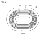
- FIG. 2 is a plan view of printed wiring board 100 .
- 3 is a bottom view of printed wiring board 100.
- FIG. 4A to 4D are process diagrams showing a method for manufacturing printed wiring board 100.
- FIG. 5 is a cross-sectional view for explaining the seed layer forming step S1.
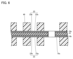
- FIG. 6 is a cross-sectional view for explaining the resist forming step S2.
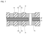
- FIG. 7 is a cross-sectional view for explaining the first electroplating step S3.
- FIG. 8 is a cross-sectional view for explaining the resist removing step S4.
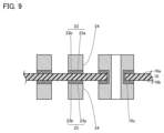
- FIG. 9 is a cross-sectional view for explaining the etching step S5.
- FIG. 10 is a cross-sectional view for explaining the second electroplating step S6.
- FIG. 11 is a cross-sectional view of the coil device 200.
- FIG. FIG. 12 is a graph showing the relationship between the value obtained by multiplying the ratio R1 by the ratio R2 and the performance of each sample.
- the pattern density of the first conductive pattern and the pattern density of the second conductive pattern can be increased as the pitch between adjacent portions of the first conductive pattern and the pitch between adjacent portions of the second conductive pattern become smaller. , the thrust generated by the coil device using the printed wiring board described in Patent Document 1 is improved.
- the electrical resistance value of the first conductive pattern per unit length and the electrical resistance value of the second conductive pattern per unit length decrease. Therefore, even if the pattern density of the first conductive pattern and the pattern density of the second conductive pattern are increased, an increase in the electrical resistance value of the entire first conductive pattern and the electrical resistance value of the entire second conductive pattern can be suppressed. .
- the printed wiring board described in Patent Document 1 it is difficult to fine-pitch the first conductive pattern and the second conductive pattern and increase the thickness of the first conductive pattern and the second conductive pattern. Therefore, the printed wiring board described in Patent Literature 1 has room for improvement in thrust and electrical resistance when used in a coil device.
- the present disclosure has been made in view of the problems of the prior art as described above. More specifically, the present disclosure provides a coil system with improved thrust and electrical resistance.
- a coil device includes a plurality of printed wiring boards and an adhesive layer.
- the plurality of printed wiring boards are stacked in the thickness direction of the coil device.
- Each of the plurality of printed wiring boards includes a base film including a first main surface and a second main surface, and a coil wiring spirally formed on at least one of the first main surface and the second main surface. have.
- the adhesive layer is arranged between a plurality of printed wiring boards adjacent in the thickness direction of the coil device.
- the thickness of the coil device is the sum of the sum of the thickness of the coil wiring and the thickness of the base film for a plurality of printed wiring boards and the thickness of the adhesive layer.
- the coil system has a portion that satisfies equation (1).
- R1 is the average value obtained by dividing the width of the coil wiring by the pitch between two adjacent coil wirings for a plurality of printed wiring boards.
- R2 is a value obtained by dividing the thickness of the coil wiring by the thickness of the coil device and totaling the values for a plurality of printed wiring boards.
- a printed wiring board includes a base film having a first main surface and a second main surface, and coil wiring spirally formed on the first main surface and the second main surface. Prepare.
- the printed wiring board has a portion that satisfies equation (2).
- R3 is the width of the coil wire divided by the pitch between two adjacent coil wire portions.
- R4 is the thickness of the coil wiring on the first main surface and the second main surface occupying the distance between the upper surface of the coil wiring on the first main surface and the upper surface of the coil wiring on the second main surface; is the ratio of
- a printed wiring board includes a base film having a first main surface and a second main surface, and coil wiring spirally formed on the first main surface and the second main surface. and a protective layer arranged on the first main surface and the second main surface so as to cover the coil wiring.
- the printed wiring board has a portion that satisfies equation (3).
- R3 is the width of the coil wire divided by the pitch between two adjacent coil wire portions.
- R5 is the ratio of the thickness of the coil wiring on the first main surface and the second main surface to the thickness of the printed wiring board.
- the printed wiring board of (3) may have a portion that satisfies the expression (4).
- the protective layer may have an adhesive layer covering the coil wiring.
- the adhesive layer may have a thickness of 10 ⁇ m or more and 25 ⁇ m or less.
- the coil wiring may have a portion that satisfies Expression (5).
- W is the width of the coil wiring.
- P is the pitch between two portions of adjacent coil wiring.
- the coil wiring may have a portion where the thickness of the coil wiring is 40 ⁇ m or more and 60 ⁇ m or less.
- the coil wiring may have a portion where the width of the coil wiring is 20 ⁇ m or more and 40 ⁇ m or less.
- a printed wiring board (referred to as “printed wiring board 100”) according to the first embodiment will be described.
- FIG. 1 is a cross-sectional view of printed wiring board 100 .
- FIG. 2 is a plan view of printed wiring board 100 .
- 3 is a bottom view of printed wiring board 100.
- illustration of the protective layer 30 is omitted.
- FIG. 3 shows printed wiring board 100 viewed from the opposite side of FIG.
- printed wiring board 100 has base film 10 , coil wiring 20 , and protective layer 30 .
- the base film 10 has a first main surface 10a and a second main surface 10b.
- the first main surface 10a and the second main surface 10b are end surfaces of the base film 10 in the thickness direction.
- the second principal surface 10b is the opposite surface of the first principal surface 10a.
- the base film 10 is made of a flexible, electrically insulating material.
- the base film 10 is made of, for example, polyimide, polyethylene terephthalate, and fluororesin.
- a portion of the coil wiring 20 on the first main surface 10a is referred to as a first coil wiring 21.
- a portion of the coil wiring 20 on the second main surface 10b is referred to as a second coil wiring 22.
- the first coil wiring 21 is spirally formed on the first main surface 10a.
- the second coil wiring 22 is spirally formed on the second main surface 10b.
- the first coil wiring 21 and the second coil wiring 22 are electrically connected to each other.
- the coil wiring 20 does not have to have either the first coil wiring 21 or the second coil wiring 22 .
- the coil wiring 20 has a seed layer 23 , a first electroplating layer 24 and a second electroplating layer 25 .
- the seed layer 23 is arranged on the main surfaces (first main surface 10a, second main surface 10b) of the base film 10 .
- the first electroplating layer 24 is arranged on the seed layer 23 .
- the second electroplating layer 25 covers the seed layer 23 and the first electroplating layer 24 . From another point of view, the second electrolytic plated layer 25 is arranged on the side surfaces of the seed layer 23 and on the side surfaces and the upper surface of the first electrolytic plated layer 24 .
- the seed layer 23 has a first layer 23a and a second layer 23b.
- the first layer 23a is arranged on the main surfaces (first main surface 10a, second main surface 10b) of the base film 10 .
- the second layer 23b is arranged on the first layer 23a.
- the first layer 23a is, for example, a sputtered layer (a layer formed by sputtering) made of a nickel-chromium alloy.
- the second layer 23b is, for example, an electroless plating layer (a layer formed by electroless plating) made of copper.
- the first electrolytic plated layer 24 is, for example, an electrolytic plated layer (a layer formed by electrolytic plating) made of the same material (copper) as the second layer 23b.
- the second electrolytic plated layer 25 is an electrolytic plated layer made of copper, for example.
- the coil wiring 20 (the first coil wiring 21 and the second coil wiring 22) functions as a coil and generates a magnetic field when current flows between the lands 21a and 22b.
- a through hole 10 c is formed in the base film 10 .
- the through hole 10c penetrates the base film 10 along the thickness direction.
- the through hole 10c overlaps the land 21b and the land 22a in plan view.
- the first coil wiring 21 and the second coil wiring 22 are electrically connected to each other by the second layer 23b, the first electroplating layer 24 and the second electroplating layer 25 arranged on the inner wall surface of the through hole 10c. It is
- the protective layer 30 disposed on the first main surface 10a is referred to as a protective layer 31.
- the protective layer 32 is arranged on the second main surface 10b.
- the protective layer 31 has, for example, an adhesive layer 31a and a protective film 31b.
- the adhesive layer 31 a is arranged on the first major surface 10 a so as to cover the first coil wiring 21 .
- the protective film 31b is arranged on the adhesive layer 31a.
- the protective layer 32 has, for example, an adhesive layer 32a and a protective film 32b.
- the adhesive layer 32 a is arranged on the second main surface 10 b so as to cover the second coil wiring 22 .
- the protective film 32b is arranged on the adhesive layer 32a.
- the adhesive layer 31a and the adhesive layer 32a are made of, for example, an epoxy-based adhesive.
- the protective film 31b and the protective film 32b are made of polyimide, for example.
- Protective layer 30 (protective layer 31, protective layer 32) may be a solder resist.
- width W be the width of the coil wiring 20 .
- a pitch P is a pitch between two portions of adjacent coil wirings 20 .
- the thickness of printed wiring board 100 excluding protective layer 30 (protective layer 31, protective layer 32) is assumed to be thickness T1.
- the thickness T1 is the distance between the top surface of the first coil wiring 21 and the top surface of the second coil wiring 22 .
- the top surface of the first coil wiring 21 is the surface of the first coil wiring 21 opposite to the base film 10
- the top surface of the second coil wiring 22 is the surface of the second coil wiring 22 opposite to the base film 10 . It is the surface.
- the thickness of the first coil wiring 21 is assumed to be thickness T2.
- the thickness of the second coil wiring 22 is assumed to be thickness T3.
- the value obtained by dividing the width W by the pitch P is defined as a ratio R3, and the ratio of the sum of the thickness T2 and the thickness T3 to the thickness T1 (the sum of the thickness T2 and the thickness T3 divided by the thickness T1) is defined as Let the ratio be R4.
- the value obtained by multiplying the ratio R3 by the ratio R4 is 0.35 or more and 0.85 or less. However, in all parts of printed wiring board 100, the value obtained by multiplying ratio R3 by ratio R4 does not have to be 0.35 or more and 0.85 or less. In a part of printed wiring board 100, the value obtained by multiplying ratio R3 by ratio R4 should be 0.35 or more and 0.85 or less.
- the thickness of printed wiring board 100 is assumed to be thickness T4.
- the ratio of the sum of the thicknesses T2 and T3 to the thickness T4 (the value obtained by dividing the sum of the thicknesses T2 and T3 by the thickness T4) is defined as a ratio R5.
- the value obtained by multiplying the ratio R3 by the ratio R5 is 0.30 or more and 0.90 or less.
- the value obtained by multiplying the ratio R3 by the ratio R5 is preferably 0.40 or more and 0.65 or less. However, in all parts of printed wiring board 100, the value obtained by multiplying ratio R3 by ratio R5 does not have to be 0.30 or more and 0.90 or less (or 0.40 or more and 0.65 or less). In a part of printed wiring board 100, the value obtained by multiplying ratio R3 by ratio R5 should be 0.30 or more and 0.90 or less (or 0.40 or more and 0.65 or less).
- the ratio R3 is, for example, 0.72 or more and 0.93 or less.
- the coil wiring 20 (the first coil wiring 21 and the second coil wiring 22) may have a portion where the ratio R3 is 0.72 or more and 0.93 or less.
- the thickness T2 and the thickness T3 are, for example, 40 ⁇ m or more and 60 ⁇ m or less.
- the first coil wire 21 may have a portion with a thickness T2 of 40 ⁇ m or more and 60 ⁇ m or less
- the second coil wire 22 may have a portion with a thickness T3 of 40 ⁇ m or more and 60 ⁇ m or less.
- the width W is, for example, 20 ⁇ m or more and 40 ⁇ m or less.
- the coil wiring 20 (the first coil wiring 21 and the second coil wiring 22) may have a portion with a width W of 20 ⁇ m or more and 40 ⁇ m or less.
- the width of the adhesive layer 31a (adhesive layer 32a) is assumed to be a thickness T5.
- the thickness T5 is the distance between the upper surface of the first coil wiring 21 (second coil wiring 22) and the protective film 31b (protective film 32b).
- the thickness T5 is preferably 10 ⁇ m or more and 25 ⁇ m or less.
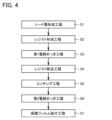
- the method for manufacturing printed wiring board 100 includes a seed layer forming step S1, a resist forming step S2, a first electroplating step S3, a resist removing step S4, and an etching step S5. , a second electroplating step S6 and a protective film attaching step S7.
- the resist forming step S2 is performed after the seed layer forming step S1.
- the first electroplating step S3 is performed after the resist forming step S2.
- the resist removing step S4 is performed after the first electroplating step S3.
- the etching step S5 is performed after the resist removing step S4.
- the second electroplating step S6 is performed after the etching step S5.
- the protective film attaching step S7 is performed after the second electroplating step S6.
- FIG. 5 is a cross-sectional view for explaining the seed layer forming step S1.
- a seed layer 23 is formed in the seed layer forming step S1.
- a first layer 23a is formed on the main surfaces of the base film 10 (the first main surface 10a and the second main surface 10b).
- the first layer 23a is formed by sputtering, for example.
- the through holes 10c are formed.
- the through holes 10c are formed by, for example, irradiating the base film 10 with a laser.
- the second layer 23b is formed on the first layer 23a.
- the second layer 23b is also formed on the inner wall surface of the through hole 10c.
- the second layer 23b is formed by electroless plating, for example.
- FIG. 6 is a cross-sectional view for explaining the resist forming step S2.
- a resist 40 is formed on the seed layer 23 in the resist forming step S2.
- the resist 40 is formed, for example, by applying a dry film resist onto the seed layer 23 and patterning the applied dry film resist by exposing and developing it.
- FIG. 7 is a cross-sectional view explaining the first electroplating step S3.
- the first electroplating layer 24 is formed on the seed layer 23 exposed through the opening of the resist 40.
- the first electroplating layer 24 is also formed on the second layer 23b on the inner wall surface of the through hole 10c.
- the first electrolytic plated layer 24 is formed by energizing the seed layer 23 in a plating solution containing the constituent material of the first electrolytic plated layer 24 .
- FIG. 8 is a cross-sectional view for explaining the resist removing step S4. As shown in FIG. 8, the resist 40 is removed in the resist removing step S4.
- FIG. 9 is a cross-sectional view for explaining the etching step S5. As shown in FIG. 9, in the etching step S5, the seed layer 23 exposed between two portions of the adjacent first electroplating layers 24 is removed by etching.
- the second layer 23b is etched.
- Etching of the second layer 23b is performed by supplying an etchant between two adjacent portions of the first electroplating layer 24 .
- the etchant is selected so that etching is rate-determined by the reaction between the reactive species in the etchant and the object to be etched rather than the diffusion of the reactive species in the etchant to the vicinity of the object to be etched.
- the etchant used is an etchant that has a dissolution reaction rate of 1.0 ⁇ m/min or less for the material (that is, copper) forming the second layer 23b.
- the etching solution include sulfuric acid hydrogen peroxide aqueous solution and sodium peroxodisulfate aqueous solution. The dissolution reaction rate of the etchant is measured based on the weight of copper reduced after etching and the etching time.
- the first layer 23a is etched.
- the etchant is switched.
- an etchant having a high selectivity with respect to the material (that is, the nickel-chromium alloy) forming the first layer 23a is used. Therefore, after switching the etchant, the etching of the first electroplating layer 24 is difficult to proceed.
- FIG. 10 is a cross-sectional view for explaining the second electroplating step S6.
- the second electroplating layer 25 is formed so as to cover the seed layer 23 and the first electroplating layer 24.
- the second electrolytic plated layer 25 is also formed on the first electrolytic plated layer 24 on the inner wall surface of the through hole 10c with the second layer 23b interposed therebetween.
- the second electroplating layer 25 is formed by energizing the seed layer 23 and the first electroplating layer 24 in the plating solution containing the constituent material of the second electroplating layer 25 .
- the coil wiring 20 (the first coil wiring 21 and the second coil wiring 22) is formed using the semi-additive method.
- the protective layer 30 is formed.
- the protective film applying step S7 first, the protective film 31b coated with the adhesive layer 31a is arranged on the first main surface 10a so as to cover the first coil wiring 21, and the adhesive layer 32a is applied.
- a protective film 32b is disposed on the second major surface 10b so as to cover the second coil wiring 22. As shown in FIG. At this stage, the adhesive layer 31a and the adhesive layer 32a are uncured.
- the protective films 31b and 32b are pressed toward the base film 10 while being heated.
- the adhesive layer 31a and the adhesive layer 32a are cured, and the protective film 31b and the protective film 32b are attached to the base film 10.
- the printed wiring board 100 having the structure shown in FIG. 1 is manufactured.
- an etchant having a low dissolution reaction rate with respect to the material forming the second layer 23b is used in the etching step S5.
- the etching in the etching step S5 is rate-determined by the reaction between the reactive species in the etchant and the etching target, and the etchant is less likely to be supplied between the two adjacent portions of the first electrolytic plating layer 24.
- variations in the etching of the second layer 23b are less likely to occur.
- the pattern density and thickness of the coil wiring 20, that is, the ratio R3 and the ratio R4 (ratio R5) can be increased.
- the printed wiring board 100 when used in a coil device, it is possible to increase the thrust while suppressing an increase in the electrical resistance value.
- coil device 200 A coil device (referred to as "coil device 200") according to the second embodiment will be described.
- FIG. 11 is a cross-sectional view of the coil device 200.
- the coil device 200 has a first surface 200a and a second surface 200b.
- the second surface 200b is the opposite surface of the first surface 200a.
- the first surface 200a and the second surface 200b are end surfaces of the coil device 200 in the thickness direction.
- the coil device 200 has multiple printed wiring boards 100 and an adhesive layer 110 .
- a plurality of printed wiring boards 100 are stacked in the thickness direction of coil device 200 .
- Adhesive layer 110 is arranged between two printed wiring boards 100 adjacent in the thickness direction of coil device 200 .
- the coil wiring 20 may be formed on at least one of the first main surface 10a and the second main surface 10b.
- Protective layer 31 is disposed only on first main surface 10a of printed wiring board 100 closest to first surface 200a, and protective layer 32 is disposed on the second main surface 10a of printed wiring board 100 closest to second surface 200b. It is arranged only on the second main surface 10b.
- the thickness of the coil device 200 is assumed to be thickness T6.
- the thickness T6 is the sum of the thickness of the coil wiring 20 and the thickness of the base film 10 for a plurality of printed wiring boards 100 and the thickness of the adhesive layer 110 (when the number of adhesive layers 110 is plural, the adhesive (total thickness of layer 110).
- a value obtained by dividing the thickness of the coil wiring 20 by the thickness T6 and totaling the values for the plurality of printed wiring boards 100 is defined as a ratio R2.
- the value obtained by multiplying the ratio R1 by the ratio R2 is 0.35 or more and 0.85 or less. In all parts of the coil device 200, the value obtained by multiplying the ratio R1 by the ratio R2 does not have to be 0.35 or more and 0.85 or less. In a part of the coil device 200, the value obtained by multiplying the ratio R1 by the ratio R2 should be 0.35 or more and 0.85 or less.
- Coil device 200 preferably has a portion where the value obtained by multiplying ratio R1 by ratio R2 is 0.38 or more. More preferably, there is a portion where the value obtained by multiplying the ratio R1 by the ratio R2 is 0.49 or more.
- the pattern density and thickness of the coil wiring 20, that is, the ratio R1 and the ratio R2 can be increased, so that the thrust can be increased while suppressing an increase in the electrical resistance value.
- samples 1 to 12 were prepared.
- the value obtained by multiplying the ratio R1 by the ratio R2, the electrical resistance value, and the thickness T6 were changed. Details of Samples 1 through 12 are shown in Table 1.
- each sample as a coil device was evaluated by dividing the inductance of each sample by the product of the electrical resistance value and thickness T6 of each sample. Since the inductance of the coil device is roughly proportional to the thrust of the coil device, it serves as an index of the thrust generated by the coil device. As the thickness of the coil device increases, the electrical resistance and thrust of the coil device tend to increase. Therefore, the larger the value obtained by dividing the inductance of the coil device by the product of the thrust and the electrical resistance of the coil device, the more the coil device increases the thrust while suppressing the increase in the electrical resistance.
- a measuring instrument used to measure the electrical resistance and inductance of each sample has a first probe and a second probe. A first probe and a second probe are respectively contacted to one end and the other end of the coil circuit of each sample. This measuring instrument measures the current flowing in the coil circuit of each sample with an alternating voltage of 100 mV and 100 kHz applied between the first probe and the second probe, and based on the measured current, each sample The electrical resistance and inductance of are calculated.
- FIG. 12 is a graph showing the relationship between the value obtained by multiplying the ratio R1 by the ratio R2 and the performance of each sample.
- the horizontal axis is the value obtained by multiplying the ratio R1 by the ratio R2.
- the vertical axis represents the value (unit: ⁇ H/( ⁇ m ⁇ )) obtained by dividing the inductance of each sample by the product of the thickness T6 of each sample and the electrical resistance value.
- the value obtained by multiplying the ratio R1 by the ratio R2 was within the range of 0.35 or more and 0.85 or less. On the other hand, in sample 1, the value obtained by multiplying the ratio R1 by the ratio R2 was less than 0.35. In samples 2 to 12, the value obtained by dividing the inductance by the product of the thickness T6 and the electrical resistance value was 0.002 ⁇ H/( ⁇ m ⁇ ) or more. On the other hand, in sample 1, the value obtained by dividing the inductance by the product of the thickness T6 and the electrical resistance value was 0.002 ⁇ H/( ⁇ m ⁇ ) or less.
- the value obtained by dividing the inductance by the product of the thickness T6 and the electrical resistance value rapidly increased within the range where the value obtained by multiplying the ratio R1 by the ratio R2 was 0.35 or more. . Therefore, by setting the value obtained by multiplying the ratio R1 by the ratio R2 to be 0.35 or more, it is possible to particularly increase the thrust of the coil device 200 while suppressing an increase in the electrical resistance value of the coil device 200. It became clear.
Landscapes
- Engineering & Computer Science (AREA)
- Power Engineering (AREA)
- Microelectronics & Electronic Packaging (AREA)
- Manufacturing & Machinery (AREA)
- Coils Or Transformers For Communication (AREA)
Priority Applications (3)
| Application Number | Priority Date | Filing Date | Title |
|---|---|---|---|
| US18/723,532 US20250062061A1 (en) | 2022-01-05 | 2022-12-22 | Coil device and printed wiring board |
| JP2023572429A JPWO2023132262A1 (https=) | 2022-01-05 | 2022-12-22 | |
| CN202280087019.7A CN118475994A (zh) | 2022-01-05 | 2022-12-22 | 线圈装置及印刷布线板 |
Applications Claiming Priority (4)
| Application Number | Priority Date | Filing Date | Title |
|---|---|---|---|
| JP2022-000510 | 2022-01-05 | ||
| JP2022000510 | 2022-01-05 | ||
| JP2022020718 | 2022-02-14 | ||
| JP2022-020718 | 2022-09-28 |
Publications (1)
| Publication Number | Publication Date |
|---|---|
| WO2023132262A1 true WO2023132262A1 (ja) | 2023-07-13 |
Family
ID=87073582
Family Applications (1)
| Application Number | Title | Priority Date | Filing Date |
|---|---|---|---|
| PCT/JP2022/047444 Ceased WO2023132262A1 (ja) | 2022-01-05 | 2022-12-22 | コイル装置及びプリント配線板 |
Country Status (4)
| Country | Link |
|---|---|
| US (1) | US20250062061A1 (https=) |
| JP (1) | JPWO2023132262A1 (https=) |
| TW (1) | TW202344154A (https=) |
| WO (1) | WO2023132262A1 (https=) |
Citations (2)
| Publication number | Priority date | Publication date | Assignee | Title |
|---|---|---|---|---|
| WO2018034161A1 (ja) * | 2016-08-18 | 2018-02-22 | 株式会社村田製作所 | 積層コイルおよびその製造方法 |
| WO2020175476A1 (ja) * | 2019-02-27 | 2020-09-03 | 住友電工プリントサーキット株式会社 | プリント配線板及びプリント配線板の製造方法 |
Family Cites Families (8)
| Publication number | Priority date | Publication date | Assignee | Title |
|---|---|---|---|---|
| US8513535B2 (en) * | 2009-10-30 | 2013-08-20 | Kyocera Corporation | Circuit board and structure using the same |
| JP2011151367A (ja) * | 2009-12-25 | 2011-08-04 | Sony Corp | 回路基板積層モジュール及び電子機器 |
| US9287034B2 (en) * | 2012-02-27 | 2016-03-15 | Ibiden Co., Ltd. | Printed wiring board, inductor component, and method for manufacturing inductor component |
| JP2014007339A (ja) * | 2012-06-26 | 2014-01-16 | Ibiden Co Ltd | インダクタ部品、その製造方法及びプリント配線板 |
| JP2014032978A (ja) * | 2012-07-31 | 2014-02-20 | Ibiden Co Ltd | インダクタ部品、インダクタ部品の製造方法及び配線板 |
| JP6170790B2 (ja) * | 2013-09-13 | 2017-07-26 | 新光電気工業株式会社 | 配線基板及びその製造方法 |
| US11521785B2 (en) * | 2016-11-18 | 2022-12-06 | Hutchinson Technology Incorporated | High density coil design and process |
| WO2023149352A1 (ja) * | 2022-02-07 | 2023-08-10 | 株式会社村田製作所 | コイル、インダクタ部品およびインダクタアレイ |
-
2022
- 2022-12-22 JP JP2023572429A patent/JPWO2023132262A1/ja active Pending
- 2022-12-22 WO PCT/JP2022/047444 patent/WO2023132262A1/ja not_active Ceased
- 2022-12-22 US US18/723,532 patent/US20250062061A1/en active Pending
- 2022-12-23 TW TW111149790A patent/TW202344154A/zh unknown
Patent Citations (2)
| Publication number | Priority date | Publication date | Assignee | Title |
|---|---|---|---|---|
| WO2018034161A1 (ja) * | 2016-08-18 | 2018-02-22 | 株式会社村田製作所 | 積層コイルおよびその製造方法 |
| WO2020175476A1 (ja) * | 2019-02-27 | 2020-09-03 | 住友電工プリントサーキット株式会社 | プリント配線板及びプリント配線板の製造方法 |
Also Published As
| Publication number | Publication date |
|---|---|
| JPWO2023132262A1 (https=) | 2023-07-13 |
| US20250062061A1 (en) | 2025-02-20 |
| TW202344154A (zh) | 2023-11-01 |
Similar Documents
| Publication | Publication Date | Title |
|---|---|---|
| CN101414464B (zh) | 布线电路基板 | |
| CN101304635B (zh) | 布线电路基板 | |
| US7629540B2 (en) | Wired circuit board and production method thereof | |
| JP4865453B2 (ja) | 配線回路基板およびその製造方法 | |
| CN102006716B (zh) | 布线电路基板及其制造方法 | |
| US20080190652A1 (en) | Wired circuit board and method for producing the same | |
| JP7803975B2 (ja) | コイル装置 | |
| WO2023132278A1 (ja) | コイル装置及びプリント配線板 | |
| WO2018211733A1 (ja) | プリント配線板及びその製造方法 | |
| JP5651933B2 (ja) | サスペンション用基板およびその製造方法 | |
| WO2019172123A1 (ja) | 配線基板およびその製造方法 | |
| US20080180928A1 (en) | Printed circuit board and manufacturing method thereof | |
| WO2023132262A1 (ja) | コイル装置及びプリント配線板 | |
| CN101754580B (zh) | 配线电路基板及其连接构造 | |
| JP4128998B2 (ja) | 配線回路基板およびその製造方法 | |
| CN118475994A (zh) | 线圈装置及印刷布线板 | |
| US20150027761A1 (en) | Printed circuit board and method of manufacturing the same | |
| JP7629102B2 (ja) | プリント配線板 | |
| JP7563600B2 (ja) | プリント配線板 | |
| JP7400989B2 (ja) | コイル装置 | |
| WO2026088293A1 (ja) | プリント配線板 | |
| WO2023276817A1 (ja) | プリント配線板 | |
| WO2023243501A1 (ja) | プリント配線板 | |
| CN118511233A (zh) | 线圈装置及印刷布线板 | |
| JP2025003596A (ja) | 配線回路基板 |
Legal Events
| Date | Code | Title | Description |
|---|---|---|---|
| 121 | Ep: the epo has been informed by wipo that ep was designated in this application |
Ref document number: 22918846 Country of ref document: EP Kind code of ref document: A1 |
|
| ENP | Entry into the national phase |
Ref document number: 2023572429 Country of ref document: JP Kind code of ref document: A |
|
| WWE | Wipo information: entry into national phase |
Ref document number: 18723532 Country of ref document: US |
|
| WWE | Wipo information: entry into national phase |
Ref document number: 202280087019.7 Country of ref document: CN |
|
| NENP | Non-entry into the national phase |
Ref country code: DE |
|
| 122 | Ep: pct application non-entry in european phase |
Ref document number: 22918846 Country of ref document: EP Kind code of ref document: A1 |