WO2023132118A1 - リニア電源回路及び車両 - Google Patents
リニア電源回路及び車両 Download PDFInfo
- Publication number
- WO2023132118A1 WO2023132118A1 PCT/JP2022/040105 JP2022040105W WO2023132118A1 WO 2023132118 A1 WO2023132118 A1 WO 2023132118A1 JP 2022040105 W JP2022040105 W JP 2022040105W WO 2023132118 A1 WO2023132118 A1 WO 2023132118A1
- Authority
- WO
- WIPO (PCT)
- Prior art keywords
- output
- voltage
- transistor
- power supply
- output transistor
- Prior art date
- Legal status (The legal status is an assumption and is not a legal conclusion. Google has not performed a legal analysis and makes no representation as to the accuracy of the status listed.)
- Ceased
Links
Images







Classifications
-
- G—PHYSICS
- G05—CONTROLLING; REGULATING
- G05F—SYSTEMS FOR REGULATING ELECTRIC OR MAGNETIC VARIABLES
- G05F3/00—Non-retroactive systems for regulating electric variables by using an uncontrolled element, or an uncontrolled combination of elements, such element or such combination having self-regulating properties
- G05F3/02—Regulating voltage or current
- G05F3/08—Regulating voltage or current wherein the variable is DC
- G05F3/10—Regulating voltage or current wherein the variable is DC using uncontrolled devices with non-linear characteristics
- G05F3/16—Regulating voltage or current wherein the variable is DC using uncontrolled devices with non-linear characteristics being semiconductor devices
- G05F3/20—Regulating voltage or current wherein the variable is DC using uncontrolled devices with non-linear characteristics being semiconductor devices using diode- transistor combinations
- G05F3/26—Current mirrors
- G05F3/262—Current mirrors using field-effect transistors only
-
- B—PERFORMING OPERATIONS; TRANSPORTING
- B60—VEHICLES IN GENERAL
- B60R—VEHICLES, VEHICLE FITTINGS, OR VEHICLE PARTS, NOT OTHERWISE PROVIDED FOR
- B60R16/00—Electric or fluid circuits specially adapted for vehicles and not otherwise provided for; Arrangement of elements of electric or fluid circuits specially adapted for vehicles and not otherwise provided for
- B60R16/02—Electric or fluid circuits specially adapted for vehicles and not otherwise provided for; Arrangement of elements of electric or fluid circuits specially adapted for vehicles and not otherwise provided for electric constitutive elements
- B60R16/03—Electric or fluid circuits specially adapted for vehicles and not otherwise provided for; Arrangement of elements of electric or fluid circuits specially adapted for vehicles and not otherwise provided for electric constitutive elements for supply of electrical power to vehicle subsystems or for
-
- G—PHYSICS
- G05—CONTROLLING; REGULATING
- G05F—SYSTEMS FOR REGULATING ELECTRIC OR MAGNETIC VARIABLES
- G05F1/00—Automatic systems in which deviations of an electric quantity from one or more predetermined values are detected at the output of the system and fed back to a device within the system to restore the detected quantity to its predetermined value or values, i.e. retroactive systems
- G05F1/10—Regulating voltage or current
- G05F1/46—Regulating voltage or current wherein the variable actually regulated by the final control device is DC
- G05F1/56—Regulating voltage or current wherein the variable actually regulated by the final control device is DC using semiconductor devices in series with the load as final control devices
-
- G—PHYSICS
- G05—CONTROLLING; REGULATING
- G05F—SYSTEMS FOR REGULATING ELECTRIC OR MAGNETIC VARIABLES
- G05F1/00—Automatic systems in which deviations of an electric quantity from one or more predetermined values are detected at the output of the system and fed back to a device within the system to restore the detected quantity to its predetermined value or values, i.e. retroactive systems
- G05F1/10—Regulating voltage or current
- G05F1/46—Regulating voltage or current wherein the variable actually regulated by the final control device is DC
- G05F1/56—Regulating voltage or current wherein the variable actually regulated by the final control device is DC using semiconductor devices in series with the load as final control devices
- G05F1/575—Regulating voltage or current wherein the variable actually regulated by the final control device is DC using semiconductor devices in series with the load as final control devices characterised by the feedback circuit
-
- G—PHYSICS
- G05—CONTROLLING; REGULATING
- G05F—SYSTEMS FOR REGULATING ELECTRIC OR MAGNETIC VARIABLES
- G05F1/00—Automatic systems in which deviations of an electric quantity from one or more predetermined values are detected at the output of the system and fed back to a device within the system to restore the detected quantity to its predetermined value or values, i.e. retroactive systems
- G05F1/10—Regulating voltage or current
- G05F1/46—Regulating voltage or current wherein the variable actually regulated by the final control device is DC
- G05F1/56—Regulating voltage or current wherein the variable actually regulated by the final control device is DC using semiconductor devices in series with the load as final control devices
- G05F1/59—Regulating voltage or current wherein the variable actually regulated by the final control device is DC using semiconductor devices in series with the load as final control devices including plural semiconductor devices as final control devices for a single load
Definitions
- the invention disclosed in this specification relates to a linear power supply circuit and a vehicle equipped with the linear power supply circuit.
- Linear power supply circuits such as LDO [low drop out] are used as power supply means for various devices.
- the linear power supply circuit be capable of phase compensation without significantly increasing the circuit area even if the capacitance value of the output capacitor is reduced.
- Patent Document 1 can be cited as an example of conventional technology related to the above.
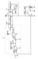
- FIG. 10 is a diagram showing a conventional linear power supply circuit according to Patent Document 1.
- FIG. 10 is a diagram showing a conventional linear power supply circuit according to Patent Document 1.
- a conventional linear power supply circuit includes an input terminal T1, an output terminal T2, a first output transistor 1, a driver 2, a reference voltage generator 3, and a phase compensation circuit 8. Further, an output capacitor 6 and a load 7 are externally attached to step down the input voltage VIN to generate an output voltage VOUT and supply the output voltage VOUT to the load 7 .
- the conductivity of the first output transistor 1 and the second output transistor 81 which will be described later, is controlled by the gate signal G1.
- PMOSFET P-channel type MOSFET
- the driver 2 includes a differential amplifier 21, a capacitor 22, a PMOSFET 23, a current amplifier 24, and a PMOSFET 25 forming a current mirror.
- the output of the differential amplifier 21 is applied to one end of the capacitor 22 and the ground potential is applied to the other end of the capacitor 22 . Therefore, the connection node between the differential amplifier 21 and the capacitor 22 is grounded in a high frequency band, so that the driver 2 can realize high-speed response.
- the phase compensation circuit 8 includes a second output transistor 81, a resistor 82, and a capacitor 83.
- One end of the resistor 82 is connected to the gates of the first output transistor 1 and the PMOSFET 25 forming the current mirror, and the other end of the resistor is connected to the gate of the second output transistor 81 .
- a capacitor 83 is provided between the gate and source of the second output transistor 81 .
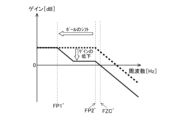
- FIG. 11 is a diagram showing gain characteristics of transfer functions of the first output transistor 1 and the phase compensation circuit 8.
- the first pole frequency FP1' is the frequency of the first pole caused by the parasitic capacitance CPD.
- the first pole of the transfer function of the first output transistor 1 is the pole to which the output capacitor 6 does not participate.
- the first output transistor 1 and the second output transistor 81 are connected in parallel, and the first output transistor 1 is not affected by the resistor 82. Therefore, the first pole frequency FP1' before shifting to the low frequency range is A pole exists at the original position, and the frequency of the pole becomes the second pole frequency FP2'. As the first pole frequency FP1' shifts to a lower frequency and the gain decreases, the zero-cross frequency FZC' shifts to a lower frequency.
- the first pole frequency FP1' and the second pole frequency FP2' are related to the second pole frequency of the transfer function of the linear power supply circuit and the output capacitor 6 shown in FIG. Therefore, the phase compensation circuit 8 can shift the second pole frequency of the transfer function of the linear power supply circuit and the output capacitor 6 shown in FIG. Due to this shift, the phase compensation circuit 8 causes the transfer function of the linear power supply circuit and the output capacitor 6 shown in FIG. can be reduced as compared with the case where the phase compensation circuit 8 is not provided. As a result, the zero-cross frequency of the transfer function of the linear power supply circuit and the output capacitor 6 shown in FIG. 10 shifts to a lower frequency. That is, the linear power supply circuit shown in FIG. 10 can perform phase compensation only by adding the phase compensation circuit 8 (without a large increase in circuit area) even when the capacitance of the output capacitor 6 is reduced.
- FIG. 12 is a diagram showing the relationship between the input voltage VIN, the gate voltages of the first output transistor 1 and the second output transistor 81, and the output voltage VOUT in the linear power supply circuit shown in FIG.
- the vertical axis of FIG. 12 is voltage, and the horizontal axis is time. That is, in FIG. 12, how the input voltage VIN, the output voltage VOUT, the gate voltage VPG (gate signal G1) driving the output transistor 1, and the gate voltage VPGF driving the second output transistor 81 change over time. indicates whether or not
- both the gate voltages VPG and VPGF start rising at time t1 when the input voltage VIN starts rising from 4.75V to 16V. While the level is rising, the gate voltage VPGF at that time is lower than the level of the gate voltage VPG, and there is a possibility that a delay time will occur compared to the rise of the gate voltage VPG. This is due to the CR circuit (resistor 82 and capacitor 83) included in the phase compensation circuit 8.
- the linear power supply circuit disclosed in this specification is provided between an input end configured to receive an input voltage and an output end configured to receive an output voltage and connected in parallel to each other. and an output stage configured to drive the first output transistor and the second output transistor based on a difference between a voltage based on the output voltage and a reference voltage.
- a driver and a potential difference suppressor configured to suppress a potential difference between a control terminal of the first output transistor and a control terminal of the second output transistor.
- the potential difference suppression unit includes an operational amplifier.
- a non-inverting input terminal of the operational amplifier is connected to the control terminal of the first output transistor, and an inverting input terminal and an output terminal of the operational amplifier are connected to the control terminal of the second output transistor.
- the operational amplifier includes a phase compensation element.
- the vehicle disclosed in this specification includes the linear power supply circuit configured as described above.
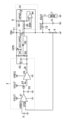
- FIG. 1 is a diagram showing a configuration example of a linear power supply circuit according to the first embodiment.
- FIG. 2 is a diagram showing a configuration example of an operational amplifier.
- FIG. 3 is a diagram showing a configuration example of a current amplifier.
- FIG. 4 is a diagram showing the relationship between the gate voltage and the output voltage of each of the first output transistor and the second output transistor in the linear power supply circuit shown in FIG.
- FIG. 5 is a diagram showing a configuration example of a linear power supply circuit according to the second embodiment.
- FIG. 6 is a diagram showing another configuration example of the current amplifier.
- FIG. 7 is a diagram showing a configuration example of a linear power supply circuit according to the third embodiment.
- FIG. 8 is a diagram showing a configuration example of a linear power supply circuit according to the fourth embodiment.
- FIG. 9A is an external view of a semiconductor integrated circuit device.
- FIG. 9B is an external view of the vehicle.
- FIG. 10 is a diagram showing a configuration example of a linear power supply circuit according to Patent Document 1. As shown in FIG. FIG. 11 is a diagram showing gain characteristics of transfer functions of the linear power supply circuit and the output capacitor shown in FIG. 12 is a diagram showing the relationship between the gate voltage and the output voltage of each of the first output transistor and the second output transistor in the linear power supply circuit shown in FIG. 10.
- a constant voltage means a voltage that is constant in an ideal state, and is actually a voltage that can slightly fluctuate due to temperature changes and the like.
- the reference voltage means a voltage that is constant in an ideal state, and is actually a voltage that can slightly fluctuate due to temperature changes and the like.
- a constant current means a current that is constant in an ideal state, and is actually a current that can slightly fluctuate due to temperature changes and the like.
- MOSFET means that the gate structure is a layer made of a conductor or a semiconductor such as polysilicon with a low resistance value, an insulating layer, and a P-type, N-type, or intrinsic semiconductor layer. ” refers to a field effect transistor consisting of at least three layers. That is, the structure of the MOSFET gate is not limited to a three-layer structure of metal, oxide, and semiconductor.
- FIG. 1 is a diagram showing a configuration example of a linear power supply circuit according to the first embodiment.
- the linear power supply circuit shown in FIG. An output capacitor 6 and a load 7 are externally attached.
- the first output transistor 1 is provided between the input terminal T1 to which the input voltage VIN is applied and the output terminal T2 to which the output voltage VOUT is applied.
- the driver 2 drives the first output transistor 1 and a second output transistor which will be described later. Specifically, the driver 2 supplies the gate signal G1 to the gate of the first output transistor 1 and to the gate of the second output transistor 81 through the resistor 82, respectively. Drives transistor 81 .
- the conductivity of the first output transistor 1 and the second output transistor 81 (in other words, the ON resistance value) is controlled by the gate signal G1.
- PMOSFETs are used as the first output transistor 1 and the second output transistor 81 in the configuration shown in FIG. Therefore, the lower the voltage level of the gate signal G1, the higher the conductivity of the first output transistor 1 and the second output transistor 81, and the higher the output voltage VOUT.
- the first output transistor 1 and the second output transistor instead of the PMOSFET, an NMOSFET or a bipolar transistor may be used.
- the driver 2 includes a differential amplifier 21 , a capacitor 22 , a PMOSFET 23 , a current amplifier 24 and a PMOSFET 25 .
- a feedback voltage VFB is applied to the inverting input terminal (-) of the differential amplifier 21, and a reference voltage VREF is applied to the non-inverting input terminal (+).
- the driver 2 increases the voltage level of the gate signal G1 as the difference value ⁇ V decreases, and conversely decreases the voltage level of the gate signal G1 as the difference value ⁇ V increases.
- the output of the differential amplifier 21 is applied to one end of the capacitor 22 and the ground potential is applied to the other end of the capacitor 22 .
- the output voltage VOUT is applied to the source of the PMOSFET 23, and the voltage based on the output of the differential amplifier 21 (connection node voltage between the differential amplifier 21 and the capacitor 22) is applied to the gate of the PMOSFET 23.
- the PMOSFET 23 converts the voltage based on the output of the differential amplifier 21 into a current and outputs it from the drain. Since the connection node between the differential amplifier 21 and the capacitor 22 is grounded in the high frequency band, the high speed response of the driver 2 can be realized.
- the withstand voltages of the differential amplifier 21 and the PMOSFET 23 are lower than the withstand voltage of the current amplifier 24. Also, the gain of the differential amplifier 21 is smaller than the gain of the current amplifier 24 . Thereby, the size reduction of the differential amplifier 21 and the PMOSFET 23 can be achieved.
- the current amplifier 24 amplifies the current Ia output from the drain of the PMOSFET 23 .
- the power supply voltage of the current amplifier 24 is a constant voltage VREG. That is, the current amplifier 24 is driven with a voltage between the constant voltage VREG and the ground potential.
- the PMOSFET 25 forms a current mirror circuit together with the first output transistor 1.
- the PMOSFET 25 converts the current Ib output from the current amplifier 24 into a voltage and supplies it to the gate of the first output transistor 1 .
- the reference voltage generator 3 generates the reference voltage VREF.
- Resistors 4 and 5 produce a feedback voltage VFB which is a voltage division of the output voltage VOUT.
- the output voltage VOUT supplied from the output terminal T2 is applied to the output capacitor 6 and the load 7.
- the phase compensation circuit 8 includes a second output transistor 81, a resistor 82, a capacitor 83, and an operational amplifier 84. Note that in a configuration in which a delay can occur between the gate potential of the first output transistor 1 and the gate potential of the second output transistor 81, the resistor 82 and the capacitor 83 are provided unlike the configuration of this embodiment. It may be a configuration without
- the second output transistor 81 is connected in parallel with the first output transistor 1 . That is, the source of the second output transistor 81 is connected to the source of the first output transistor 1 and the drain of the second output transistor 81 is connected to the drain of the first output transistor 1 .
- the size of the second output transistor 81 is made larger than the size of the first output transistor 1 so that the current flowing through the second output transistor 81 is larger than the current flowing through the first output transistor 1 .
- size means area.
- One end of the resistor 82 is connected to each gate of the first output transistor 1 and the PMOSFET 25 , and the other end of the resistor 82 is connected to the gate of the second output transistor 81 .
- a capacitor 83 is provided between the gate and source of the second output transistor 81 .
- the parasitic capacitor of the second output transistor 81 is used as the capacitor 83 .
- a capacitor different from the parasitic capacitor of the second output transistor 81 may be used as the capacitor 83. good too.
- the capacitance value of the capacitor 83 can be easily adjusted. It is desirable that the capacitance value of the capacitor 83 is larger than the capacitance value of the parasitic capacitance CPD.
- the phase compensation circuit 8 may further include a capacitor provided between the gate and drain of the second output transistor 81 .
- the operational amplifier 84 is an example of a potential difference suppression unit that suppresses the potential difference between the gate of the first output transistor 1 and the gate of the second output transistor 81 .
- the potential difference suppressing unit monitors, for example, the voltage difference between the gate voltage of the first output transistor 1 and the gate voltage of the second output transistor 81, and if the voltage difference is equal to or greater than a certain value, the first output transistor 1 or the gate voltage of the second output transistor 81 so that the potential difference between the gate of the first output transistor 1 and the gate of the second output transistor 81 becomes small. It should be configured to In this embodiment, the operational amplifier 84 outputs the control signal.
- the operational amplifier 84 has an input offset voltage 84A.
- a non-inverting input terminal of the operational amplifier 84 is connected to the gate of the first output transistor 1 .
- the inverting input terminal and output terminal of the operational amplifier 84 are connected to the gate of the first output transistor 1 .
- FIG. 2 is a diagram showing a configuration example of the operational amplifier 84. As shown in FIG. The operational amplifier 84 of the configuration example shown in FIG. and a resistor 846 and a capacitor 847 that are phase compensation elements.
- the current mirror circuit supplies the NMOSFET 841 with a first current and the NMOSFET 842 with a second current that is a mirror current of the first current.
- the source of the NMOSFET 841 is the non-inverting input terminal of the operational amplifier 84
- the source of the NMOSFET 842 is the inverting input terminal of the operational amplifier 84
- the source of the NMOSFET 845 is the output terminal of the operational amplifier 84.
- a bias voltage Vb is applied to the gates of NMOSFET 841 and NMOSFET 842 .
- the drain of NMOSFET 841 is connected to the drain of PMOSFET 843 and the gate of NMOSFET 845 .
- the drain of NMOSFET 842 is connected to the drain and gate of PMOSFET 844 and the gate of PMOSFET 843 .
- An input voltage VIN is applied to the source of PMOSFET 843, the source of PMOSFET 844, and the drain of NMOSFET 845.
- the source of NMOSFET 845 is connected to the source of NMOSFET 842 .
- the ratio of the channel width to the channel length of the NMOSFETs 841 and 842 is set to be different from each other, or the first current and the second current are set to different values (the current
- An input offset voltage 84A is generated by at least one of setting the mirror ratio of the mirror circuit to a value other than 1. With such a configuration, it is easy to make the input offset voltage 84A as designed.
- the operational amplifier 84 of the configuration example shown in FIG. 2 includes a phase compensation element, the potential difference suppression by the operational amplifier 84 becomes remarkable, and the overshoot of the output voltage VOUT can be suppressed more than when the operational amplifier 84 does not include the phase compensation element. can be done.
- One end of the resistor 846, which is the phase compensation element, is connected to the drain of the NMOSFET 845, and the capacitor 847, which is the phase compensation element, is provided between the gate and source of the NMOSFET 845.
- An input voltage VIN is applied to the other end of the resistor 846, which is a phase compensation element.
- FIG. 3 is a diagram showing a configuration example of the current amplifier 24 in the linear power supply circuit shown in FIG.
- the current amplifier 24 includes current sink type current mirror circuits CM_1, CM_2, . . . , and CM_n, and current source type current mirror circuits CM_3, . ) and Between the current sink type current mirror circuit CM_1, the constant current source CS1 that flows the constant current I1, and the current sink type current mirror circuit CM_n, the current sink type current mirror circuit and the current source type A current mirror circuit is alternately arranged to amplify the current. The amplified current becomes the current Ib that is converted into the voltage of the gate signal G1 at the final stage.
- FIG. 4 is a diagram showing the relationship between the input voltage VIN, the gate voltages of the first output transistor 1 and the second output transistor 81, and the output voltage VOUT in the linear power supply circuit shown in FIG.
- the vertical axis of FIG. 4 is voltage, and the horizontal axis is time.
- FIG. 4 how the input voltage VIN, the output voltage VOUT, the gate voltage (gate signal G1) VPG driving the first output transistor 1, and the gate voltage VPGF driving the second output transistor 81 change over time. shows that it is changing.
- both the gate voltages VPG and VPGF start to rise from time t1 when the input voltage VIN starts to rise from 4.75V to 16V, but the gate voltage VPGF rises without delaying the rise of the gate voltage VPG. That is, both the gate voltage VPG and the gate voltage VPGF increase. This is because the operational amplifier 84 suppresses the voltage difference between the gate voltage VPG and the gate voltage VPGF.
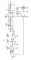
- FIG. 5 is a diagram showing the configuration of a linear power supply circuit according to the second embodiment.
- the same parts as in FIG. 1 are denoted by the same reference numerals, and detailed description thereof will be omitted.
- the driver 2 includes a differential amplifier 21', a capacitor 22', an NMOSFET 23', a current amplifier 24, and a PMOSFET 25.
- the differential amplifier 21' outputs a voltage corresponding to the difference between the feedback voltage VFB and the reference voltage VREF.
- the power supply voltage of the differential amplifier 21' is the first constant voltage VREG1. That is, the differential amplifier 21' is driven with a voltage between the first constant voltage VREG1 and the ground potential.
- the withstand voltages of the differential amplifier 21' and the NMOSFET 23' are lower than the withstand voltage of the current amplifier 24. Also, the gain of the differential amplifier 21 ′ is smaller than the gain of the current amplifier 24 . As a result, the size of the differential amplifier 21' and the NMOSFET 23' can be reduced.
- the output of the differential amplifier 21' is applied to one end of the capacitor 22', and the output voltage VOUT is applied to the other end of the capacitor 22'.
- a voltage dependent on the output voltage VOUT may be applied to the other end of the capacitor 22 instead of the output voltage VOUT.
- a ground potential is applied to the source of the NMOSFET 23', and a voltage (connection node voltage between the differential amplifier 21' and the capacitor 22') based on the output of the differential amplifier 21' is applied to the gate of the NMOSFET 23'.
- the NMOSFET 23' converts the voltage based on the output of the differential amplifier 21' into a current and outputs it from the drain. Since the connection node between the differential amplifier 21' and the capacitor 22' is grounded to the output voltage VOUT in the high frequency band, the driver 2 can realize high-speed response.
- the current amplifier 24 amplifies the current Ia output from the drain of the NMOSFET 23'.
- the power supply voltage of the current amplifier 24 is the second constant voltage VREG2. That is, the current amplifier 24 is driven with a voltage between the second constant voltage VREG2 and the ground potential.
- the first constant voltage VREG1 and the second constant voltage VREG2 may have the same value or different values. In this configuration example, since the current Ia flows from the current amplifier 24 toward the NMOSFET 23', the current amplifier 24 may have the circuit configuration shown in FIG.
- the phase compensation circuit in the linear power supply circuit according to this embodiment shown in FIG. 5 is the same as the linear power supply circuit according to the first embodiment shown in FIG. Therefore, the overshoot of the output voltage VOUT can be suppressed by the same effect. Further, the linear power supply circuit according to the present embodiment shown in FIG. 5 can ensure the operation of the differential amplifier 21' even when the set value of the output voltage VOUT is low.
- the input voltage VIN is used as the power supply voltage of the differential amplifier 21' instead of the first constant voltage VREG1
- the input voltage VIN is used instead of the second constant voltage VREG2 for the current amplifier. 24 may be used as the power supply voltage.
- FIG. 7 is a diagram showing the configuration of a linear power supply circuit according to the third embodiment.
- the linear power supply circuit shown in FIG. 7 applies a phase compensation circuit 8 to a general and well-known linear power supply circuit having a PMOS source-grounded output stage.
- the linear power supply circuit including the PMOS source-grounded output stage shown in FIG. 7 is well known as a prior art, so a detailed description will be omitted.
- the linear power supply circuit shown in FIG. 7 by suppressing the difference in conductivity between the output transistor Q1 and the second output transistor 81, overshoot of the output voltage can be suppressed.
- phase compensation circuit according to the invention disclosed in this specification can be applied not only to the linear power supply circuits according to the first and second embodiments, but also to the case where there are a plurality of output transistors.
- FIG. 8 is a diagram showing the configuration of a linear power supply circuit according to the fourth embodiment.
- the linear power supply circuit shown in FIG. 8 has a configuration in which a clamper circuit is added to the linear power supply circuit according to the first embodiment shown in FIG.
- the clamper circuit is configured to clamp the voltage applied to the gate of the second output transistor 81 .
- the clamper circuit even if the operational amplifier 84 malfunctions, it is possible to prevent the voltage applied to the gate of the second output transistor 81 from becoming excessive.
- the clamper circuit includes resistors 91 and 92 and a diode 93.
- Resistors 91 and 92 are voltage divider circuits configured to divide the difference between the input voltage VIN and the voltage applied to the gate of the first output transistor 1 .
- the anode of the diode 93 is applied with the divided voltage (the voltage generated at the connection node between the resistors 91 and 92) output from the voltage dividing circuit.
- the cathode of diode 93 is connected to the gate of second output transistor 81 .
- the clamper circuit is realized with a simple circuit configuration, it is possible to suppress an increase in cost and mounting area due to the addition of the clamper circuit.
- the clamper circuit is added to the linear power supply circuit according to the first embodiment, but the linear power supply circuit according to the second embodiment or the third embodiment is not limited to the linear power supply circuit according to the first embodiment.
- a clamper circuit may be added to the linear power supply circuit according to the embodiment.
- FIG. 9A is an external view of a semiconductor integrated circuit device.
- the semiconductor integrated circuit device shown in FIG. 9A has external pins P1 to P14 and an internal power supply 9 therein.
- the internal power supply 9 is a linear power supply circuit according to any one of the first to fourth embodiments described above. When built-in, the presence or absence of an output capacitor does not matter.
- ⁇ Application example 2> 9B is an external view of the vehicle X.
- FIG. The vehicle X of this configuration example is equipped with various electronic devices X11 to X18 that operate by receiving voltage supplied from a battery (not shown). Note that the mounting positions of the electronic devices X11 to X18 in this figure may differ from the actual positions for convenience of illustration.
- the electronic device X11 is an engine control unit that performs engine-related controls (injection control, electronic throttle control, idling control, oxygen sensor heater control, auto-cruise control, etc.).
- the electronic device X12 is a lamp control unit that controls lighting and extinguishing of HID [high intensity discharged lamp] and DRL [daytime running lamp].
- the electronic device X13 is a transmission control unit that performs controls related to the transmission.
- the electronic device X14 is a braking unit that performs control related to the movement of the vehicle X (ABS [anti-lock brake system] control, EPS [electric power steering] control, electronic suspension control, etc.).
- ABS anti-lock brake system
- EPS electric power steering
- electronic suspension control etc.
- the electronic device X15 is a security control unit that performs drive control such as door locks and security alarms.
- Electronic device X16 includes wipers, electric door mirrors, power windows, dampers (shock absorbers), electric sunroofs, electric seats, and other electronic devices built into vehicle X at the factory shipment stage as standard equipment or manufacturer options. is.
- the electronic device X17 is an electronic device that is arbitrarily attached to the vehicle X as a user option, such as an in-vehicle A/V [audio/visual] device, a car navigation system, and an ETC [electronic toll collection system].
- the electronic device X18 is an electronic device equipped with a high withstand voltage motor, such as an in-vehicle blower, oil pump, water pump, and battery cooling fan.
- a high withstand voltage motor such as an in-vehicle blower, oil pump, water pump, and battery cooling fan.
- linear power supply circuit described above can be incorporated into any of the electronic devices X11 to X18.
- phase compensation circuit is not limited to the specific circuit configuration of the phase compensation circuit 8, which is merely an example, as long as it can suppress the delay between the drive signals of the transistors connected in parallel.
- a bipolar transistor may be used instead of the MOSFET used in the above embodiments.
- first output transistors are provided between an input terminal to which an input voltage is applied and an output terminal to which an output voltage is applied, and are connected in parallel.
- the potential difference suppression unit includes an operational amplifier, a non-inverting input terminal of the operational amplifier is connected to the control terminal of the first output transistor, and an inverting input terminal and an output terminal of the operational amplifier are connected to the control terminal of the second output transistor. and the operational amplifier has a configuration (first configuration) including phase compensation elements (846, 847).
- the potential difference between the control terminal of the first output transistor and the control terminal of the second output transistor is suppressed, so overshoot of the output voltage can be suppressed.
- the operational amplifier since the operational amplifier includes the phase compensation element, the potential difference suppression by the potential difference suppressing section becomes remarkable, and overshoot of the output voltage can be suppressed more than when the operational amplifier does not include the phase compensation element.
- the operational amplifier includes an output stage transistor (845) serving as a source follower output stage or an emitter follower output stage, and the phase compensation element includes a resistor (846) and a capacitor (847).
- the resistor when the output stage transistor is the source follower output stage, the resistor is connected to the drain of the output stage transistor, the capacitor is provided between the gate and source of the output stage transistor, and the When the output stage transistor is the emitter follower output stage, the resistor is connected to the collector of the output stage transistor, and the capacitor is provided between the base and the emitter of the output stage transistor (second configuration).
- the operational amplifier may have an input offset voltage (third configuration).
- the operational amplifier operates so that the potential difference between the control terminal of the first output transistor and the control terminal of the second output transistor becomes the input offset voltage. Easy to adjust.
- the operational amplifier includes a first input differential pair transistor (841) connected to the control terminal of the first output transistor and connected to the control terminal of the second output transistor. a second input differential pair of transistors (842) that supplies a first current to said first input differential pair of transistors and a second current that is a mirror current of said first current to said second input differential pair of transistors; and a current mirror circuit (843, 844) configured to provide a current mirror circuit (843, 844), wherein the first input differential pair of transistors and the second input differential pair of transistors are both MOS transistors, and Even in a configuration (fourth configuration) in which the input offset voltage is generated by at least one of different channel width ratios and different values of the first current and the second current. good.
- the linear power supply circuit having the above fourth configuration makes it easy to set the input offset voltage to the design value.
- a configuration comprising a clamper circuit (91, 92, 93) configured to clamp the voltage applied to the control terminal of the second output transistor. (Fifth configuration).
- the linear power supply circuit having the fifth configuration can prevent the voltage applied to the control terminal of the second output transistor from becoming excessive even if a problem occurs in the potential difference suppression unit.
- the clamper circuit includes a voltage dividing circuit (91 , 92), and a diode (93) configured such that the divided voltage output from the voltage divider circuit is applied to its anode and whose cathode is connected to the control terminal of the second output transistor ( sixth configuration).
- the linear power supply circuit of the sixth configuration realizes a clamper circuit with a simple circuit configuration, so it is possible to suppress an increase in cost and mounting area due to the addition of the clamper circuit.
- the vehicle described above has a configuration (seventh configuration) including the linear power supply circuit of any one of the first to sixth configurations.
Landscapes
- Engineering & Computer Science (AREA)
- Physics & Mathematics (AREA)
- Electromagnetism (AREA)
- General Physics & Mathematics (AREA)
- Radar, Positioning & Navigation (AREA)
- Automation & Control Theory (AREA)
- Microelectronics & Electronic Packaging (AREA)
- Mechanical Engineering (AREA)
- Nonlinear Science (AREA)
- Amplifiers (AREA)
Priority Applications (2)
| Application Number | Priority Date | Filing Date | Title |
|---|---|---|---|
| JP2023572357A JPWO2023132118A1 (https=) | 2022-01-06 | 2022-10-27 | |
| US18/763,318 US20240353881A1 (en) | 2022-01-06 | 2024-07-03 | Linear power supply circuit and vehicle |
Applications Claiming Priority (2)
| Application Number | Priority Date | Filing Date | Title |
|---|---|---|---|
| JP2022000851 | 2022-01-06 | ||
| JP2022-000851 | 2022-01-06 |
Related Child Applications (1)
| Application Number | Title | Priority Date | Filing Date |
|---|---|---|---|
| US18/763,318 Continuation US20240353881A1 (en) | 2022-01-06 | 2024-07-03 | Linear power supply circuit and vehicle |
Publications (1)
| Publication Number | Publication Date |
|---|---|
| WO2023132118A1 true WO2023132118A1 (ja) | 2023-07-13 |
Family
ID=87073441
Family Applications (1)
| Application Number | Title | Priority Date | Filing Date |
|---|---|---|---|
| PCT/JP2022/040105 Ceased WO2023132118A1 (ja) | 2022-01-06 | 2022-10-27 | リニア電源回路及び車両 |
Country Status (3)
| Country | Link |
|---|---|
| US (1) | US20240353881A1 (https=) |
| JP (1) | JPWO2023132118A1 (https=) |
| WO (1) | WO2023132118A1 (https=) |
Families Citing this family (1)
| Publication number | Priority date | Publication date | Assignee | Title |
|---|---|---|---|---|
| US20250132729A1 (en) * | 2023-10-24 | 2025-04-24 | Cirrus Logic International Semiconductor Ltd. | Output current-dependent voltage regulator output stage reconfiguration |
Citations (4)
| Publication number | Priority date | Publication date | Assignee | Title |
|---|---|---|---|---|
| JPH0317811U (https=) * | 1989-06-30 | 1991-02-21 | ||
| JP2007011972A (ja) * | 2005-07-04 | 2007-01-18 | Toshiba Corp | 直流電源電圧安定化回路 |
| JP2020071710A (ja) * | 2018-10-31 | 2020-05-07 | ローム株式会社 | リニア電源回路 |
| WO2020209369A1 (ja) * | 2019-04-12 | 2020-10-15 | ローム株式会社 | リニア電源回路及びソースフォロワ回路 |
Family Cites Families (4)
| Publication number | Priority date | Publication date | Assignee | Title |
|---|---|---|---|---|
| TWI413881B (zh) * | 2010-08-10 | 2013-11-01 | Novatek Microelectronics Corp | 線性穩壓器及其電流感測電路 |
| JP5971720B2 (ja) * | 2012-11-01 | 2016-08-17 | 株式会社東芝 | 電圧レギュレータ |
| US10558232B2 (en) * | 2015-05-26 | 2020-02-11 | Sony Corporation | Regulator circuit and control method |
| DE102019201195B3 (de) * | 2019-01-30 | 2020-01-30 | Dialog Semiconductor (Uk) Limited | Rückkopplungsschema für einen stabilen LDO-Reglerbetrieb |
-
2022
- 2022-10-27 JP JP2023572357A patent/JPWO2023132118A1/ja active Pending
- 2022-10-27 WO PCT/JP2022/040105 patent/WO2023132118A1/ja not_active Ceased
-
2024
- 2024-07-03 US US18/763,318 patent/US20240353881A1/en active Pending
Patent Citations (4)
| Publication number | Priority date | Publication date | Assignee | Title |
|---|---|---|---|---|
| JPH0317811U (https=) * | 1989-06-30 | 1991-02-21 | ||
| JP2007011972A (ja) * | 2005-07-04 | 2007-01-18 | Toshiba Corp | 直流電源電圧安定化回路 |
| JP2020071710A (ja) * | 2018-10-31 | 2020-05-07 | ローム株式会社 | リニア電源回路 |
| WO2020209369A1 (ja) * | 2019-04-12 | 2020-10-15 | ローム株式会社 | リニア電源回路及びソースフォロワ回路 |
Also Published As
| Publication number | Publication date |
|---|---|
| JPWO2023132118A1 (https=) | 2023-07-13 |
| US20240353881A1 (en) | 2024-10-24 |
Similar Documents
| Publication | Publication Date | Title |
|---|---|---|
| JP7177661B2 (ja) | リニア電源回路 | |
| JP7198349B2 (ja) | リニア電源回路及びソースフォロワ回路 | |
| JP7489244B2 (ja) | リニア電源回路 | |
| JP7230249B2 (ja) | リニア電源回路 | |
| JP7295881B2 (ja) | リニア電源回路 | |
| JP7165562B2 (ja) | リニア電源回路 | |
| JP2020072399A (ja) | 差動増幅器 | |
| JP2018112963A (ja) | リニア電源 | |
| JP7420738B2 (ja) | リニア電源 | |
| WO2023132118A1 (ja) | リニア電源回路及び車両 | |
| WO2022185945A1 (ja) | リニア電源回路 | |
| JP7795343B2 (ja) | リニア電源回路及び車両 |
Legal Events
| Date | Code | Title | Description |
|---|---|---|---|
| 121 | Ep: the epo has been informed by wipo that ep was designated in this application |
Ref document number: 22918707 Country of ref document: EP Kind code of ref document: A1 |
|
| ENP | Entry into the national phase |
Ref document number: 2023572357 Country of ref document: JP Kind code of ref document: A |
|
| NENP | Non-entry into the national phase |
Ref country code: DE |
|
| 122 | Ep: pct application non-entry in european phase |
Ref document number: 22918707 Country of ref document: EP Kind code of ref document: A1 |