WO2023132002A1 - 光電変換装置、光電変換システム、移動体 - Google Patents
光電変換装置、光電変換システム、移動体 Download PDFInfo
- Publication number
- WO2023132002A1 WO2023132002A1 PCT/JP2022/000070 JP2022000070W WO2023132002A1 WO 2023132002 A1 WO2023132002 A1 WO 2023132002A1 JP 2022000070 W JP2022000070 W JP 2022000070W WO 2023132002 A1 WO2023132002 A1 WO 2023132002A1
- Authority
- WO
- WIPO (PCT)
- Prior art keywords
- signal processing
- photoelectric conversion
- substrate
- conversion device
- processing
- Prior art date
- Legal status (The legal status is an assumption and is not a legal conclusion. Google has not performed a legal analysis and makes no representation as to the accuracy of the status listed.)
- Ceased
Links
Images


Classifications
-
- H—ELECTRICITY
- H04—ELECTRIC COMMUNICATION TECHNIQUE
- H04N—PICTORIAL COMMUNICATION, e.g. TELEVISION
- H04N25/00—Circuitry of solid-state image sensors [SSIS]; Control thereof
- H04N25/70—SSIS architectures; Circuits associated therewith
- H04N25/703—SSIS architectures incorporating pixels for producing signals other than image signals
- H04N25/704—Pixels specially adapted for focusing, e.g. phase difference pixel sets
-
- H—ELECTRICITY
- H04—ELECTRIC COMMUNICATION TECHNIQUE
- H04N—PICTORIAL COMMUNICATION, e.g. TELEVISION
- H04N25/00—Circuitry of solid-state image sensors [SSIS]; Control thereof
- H04N25/70—SSIS architectures; Circuits associated therewith
- H04N25/76—Addressed sensors, e.g. MOS or CMOS sensors
- H04N25/77—Pixel circuitry, e.g. memories, A/D converters, pixel amplifiers, shared circuits or shared components
- H04N25/772—Pixel circuitry, e.g. memories, A/D converters, pixel amplifiers, shared circuits or shared components comprising A/D, V/T, V/F, I/T or I/F converters
-
- H—ELECTRICITY
- H04—ELECTRIC COMMUNICATION TECHNIQUE
- H04N—PICTORIAL COMMUNICATION, e.g. TELEVISION
- H04N25/00—Circuitry of solid-state image sensors [SSIS]; Control thereof
- H04N25/70—SSIS architectures; Circuits associated therewith
- H04N25/76—Addressed sensors, e.g. MOS or CMOS sensors
- H04N25/78—Readout circuits for addressed sensors, e.g. output amplifiers or A/D converters
-
- H—ELECTRICITY
- H04—ELECTRIC COMMUNICATION TECHNIQUE
- H04N—PICTORIAL COMMUNICATION, e.g. TELEVISION
- H04N25/00—Circuitry of solid-state image sensors [SSIS]; Control thereof
- H04N25/70—SSIS architectures; Circuits associated therewith
- H04N25/79—Arrangements of circuitry being divided between different or multiple substrates, chips or circuit boards, e.g. stacked image sensors
-
- H—ELECTRICITY
- H10—SEMICONDUCTOR DEVICES; ELECTRIC SOLID-STATE DEVICES NOT OTHERWISE PROVIDED FOR
- H10F—INORGANIC SEMICONDUCTOR DEVICES SENSITIVE TO INFRARED RADIATION, LIGHT, ELECTROMAGNETIC RADIATION OF SHORTER WAVELENGTH OR CORPUSCULAR RADIATION
- H10F30/00—Individual radiation-sensitive semiconductor devices in which radiation controls the flow of current through the devices, e.g. photodetectors
- H10F30/20—Individual radiation-sensitive semiconductor devices in which radiation controls the flow of current through the devices, e.g. photodetectors the devices having potential barriers, e.g. phototransistors
-
- H—ELECTRICITY
- H10—SEMICONDUCTOR DEVICES; ELECTRIC SOLID-STATE DEVICES NOT OTHERWISE PROVIDED FOR
- H10F—INORGANIC SEMICONDUCTOR DEVICES SENSITIVE TO INFRARED RADIATION, LIGHT, ELECTROMAGNETIC RADIATION OF SHORTER WAVELENGTH OR CORPUSCULAR RADIATION
- H10F39/00—Integrated devices, or assemblies of multiple devices, comprising at least one element covered by group H10F30/00, e.g. radiation detectors comprising photodiode arrays
- H10F39/10—Integrated devices
- H10F39/12—Image sensors
-
- G—PHYSICS
- G01—MEASURING; TESTING
- G01S—RADIO DIRECTION-FINDING; RADIO NAVIGATION; DETERMINING DISTANCE OR VELOCITY BY USE OF RADIO WAVES; LOCATING OR PRESENCE-DETECTING BY USE OF THE REFLECTION OR RERADIATION OF RADIO WAVES; ANALOGOUS ARRANGEMENTS USING OTHER WAVES
- G01S17/00—Systems using the reflection or reradiation of electromagnetic waves other than radio waves, e.g. lidar systems
- G01S17/88—Lidar systems specially adapted for specific applications
- G01S17/93—Lidar systems specially adapted for specific applications for anti-collision purposes
- G01S17/931—Lidar systems specially adapted for specific applications for anti-collision purposes of land vehicles
Definitions
- the present invention relates to a photoelectric conversion device, a photoelectric conversion system, and a moving object.
- a structure having a laminated structure in which multiple substrates are laminated is known.
- Patent Document 1 describes a laminated light receiving sensor in which a first substrate having pixels and a second substrate having a signal processing circuit (DSP) are laminated.
- the signal processing circuit executes processing based on a neural network calculation model.
- the processing signal processing circuit based on the neural network calculation model arranged on the second board consumes a large amount of power, and heat generation increases in proportion to the power consumption.
- the heat generated by the second substrate propagates to the pixel array arranged on the first substrate. This results in an increase in noise contained in the signal output by the pixel.
- local heat generation causes output unevenness in the image plane, which not only lowers the image quality, but also makes image quality correction processing difficult.
- the pixel array includes pixels that output focus detection signals, processing of the focus detection signals may hinder speeding up.
- the technology related to the present disclosure provides technology that is advantageous for dispersing heat generated on the second substrate and speeding up processing involving machine learning performed on the second substrate.
- One aspect of the present disclosure is a first substrate provided with a pixel array having a plurality of pixels including pixels that output focus detection signals; and a second board including an AD conversion section including a plurality of AD conversion circuits for converting into signals, the second board performing machine learning processing and including a first signal processing section and a second signal processing section.
- each of the plurality of sets includes a plurality of AD conversion circuits different from each other; the first signal processing section is arranged to correspond to one of the plurality of sets;
- the photoelectric conversion device is characterized in that the two-signal processing unit is arranged so as to correspond to another set of the plurality of sets.
- a photoelectric conversion device will be mainly described as an example of a photoelectric conversion device.
- each embodiment is not limited to the photoelectric conversion device, and can be applied to other examples of the photoelectric conversion device.
- a distance measuring device a device for distance measurement using focus detection or TOF (Time Of Flight)
- a photometric device a device for measuring the amount of incident light, etc.
- conductivity types of the transistors described in the embodiments described below are examples, and are not limited to the conductivity types described in the examples.
- the conductivity types described in the embodiments can be changed as appropriate, and along with this change, the potentials of the gate, source, and drain of the transistor are changed as appropriate.
- the low level and high level of the potential supplied to the gate may be reversed with respect to the description in the embodiment as the conductivity type is changed.
- the conductivity types of the semiconductor regions described in the examples below are also examples, and are not limited to the conductivity types described in the examples. The conductivity types described in the examples can be changed as appropriate, and the potentials of the semiconductor regions are changed accordingly.
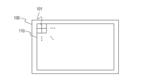
- FIG. 1A is a schematic diagram of a stacked photoelectric conversion device according to the first embodiment.
- the first substrate 100 and the second substrate 200 are semiconductor substrates, and as shown in FIG. 1B, the first substrate 100 has a pixel array portion 110 in which a plurality of unit pixels 101 are arranged over a plurality of rows and columns. are doing.
- the plurality of unit pixels 101 may be arranged in one row and multiple columns, or may be arranged in multiple columns and rows.
- the unit pixels 101 typically consist of tens of millions of pixels.
- the photoelectric conversion device of this embodiment is a backside illumination type photoelectric conversion device in which light is incident from the first substrate 100 side. Furthermore, a signal line (not shown) is provided between the photoelectric conversion section and the joint surface 300 .
- FIG. 15 is a circuit diagram showing a circuit of the unit pixel 101 of 2 rows and 1 column among the unit pixels 101 shown in FIGS. 1A and 1B.
- charges accumulated in a photodiode which is a photoelectric conversion unit, are electrons.
- all the transistors included in the unit pixel 101 are N-type transistors.
- the charges accumulated by the photodiode may be holes, and in this case, the transistor of the unit pixel 101 may be a P-type transistor.
- the definition of the conductivity type used in the following description can be changed according to the polarity of the charge treated as a signal.
- the unit pixel 101 has photodiodes D1 and D2, which are photoelectric conversion units, transfer transistors M1 and M2, a charge conversion unit C1, a reset transistor M3, an amplification transistor M4, and a selection transistor M5.
- the transfer transistor M1 is provided in an electrical path between the photodiode D1 and a node to which the charge converter C1, the reset transistor M3, and the amplification transistor M4 are connected.
- the transfer transistor M2 is provided in an electrical path between the node to which the charge converter C1, the reset transistor M3, and the amplification transistor M4 are connected, and the photodiode D2.
- the charge conversion section C1 is also called a floating diffusion section (FD section).
- a power supply voltage VDD is applied to the reset transistor M3 and the amplification transistor M4.
- the selection transistor M5 is provided in an electrical path between the amplification transistor M4 and the column signal line 10.
- FIG. It can be said that the amplification transistor M4 is electrically connected to the vertical output line 10 via the selection transistor M5.
- the charge conversion unit C1 includes a floating diffusion capacitance provided in the semiconductor substrate and a parasitic capacitance of an electrical path from the transfer transistor M1 to the amplification transistor M5 via the floating diffusion capacitance.
- Each of the signal RES, the signal Tx_A, and the signal SEL is a signal supplied via the control line 30 from the vertical scanning circuit (not shown) shown in FIGS. 1A and 1B.
- the pixel row to which the signal is supplied is added to the end of each signal.
- the signal RES(m) means the signal RES supplied to the m-th row pixels.
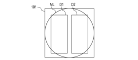
- Photodiodes D1 and D2 are arranged corresponding to one microlens ML, as shown in FIG. 16A. That is, the photodiodes D1 and D2 are arranged to receive the light transmitted through one microlens ML. Accordingly, phase difference detection type focus detection can be performed.
- All of the plurality of pixels that receive incident light provided in the pixel array may have the configuration of FIG. 16A.
- only some of the pixels may have the configuration shown in FIG. 16A, and another portion of the pixels may have one photodiode D1 shown in FIG.
- a current source (not shown) is connected to each of the vertical output lines 10-1 and 10-2.
- the selection transistor M5 of the unit pixel 101 in the m-th row is turned on.
- current is supplied from the current source to the amplification transistor M4 of the unit pixel 101 in the m-th row.
- a source follower circuit is formed by the power supply voltage VDD, the amplification transistor M4, and a current source (not shown) connected to the vertical output line 10-1.
- the amplification transistor M4 outputs a signal based on the potential of the charge converter C1 to the vertical output line 10-1 via the transistor M5.
- the selection transistor M5 of the unit pixel 101 in the m+1 row is turned on.
- current is supplied from the current source to the amplification transistor M4 in the (m+1)th row.
- a source follower circuit is formed by the power supply voltage VDD, the amplification transistor M4, and a current source (not shown) connected to the vertical output line 10-2.
- the amplification transistor M4 outputs a signal based on the potential of the charge converter C1 to the vertical output line 10-2 via the transistor M5.
- the unit pixels 101 in the m-th row and the unit pixels 101 in the m+1-th row are connected to different vertical output lines 10, respectively.
- one vertical output line 10 may be provided for one column of unit pixels 101, or the number of vertical output lines 10 may be greater than two. Also good.
- the photoelectric conversion portion may be an avalanche photodiode, and any device that performs photoelectric conversion may be used.
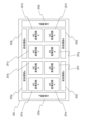
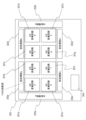
- the second substrate 200 has a plurality of AD conversion circuits 201a to 201h for converting analog signals output from the unit pixels 101 into digital signals.
- the second substrate 200 also has a plurality of preprocessing units 202a to 202d for converting the digital data output from the AD conversion circuits 201a to 201h into image data.
- the second substrate 200 further includes a plurality of AI processing units 203a and 203b, which are signal processing units for executing processing based on a neural network calculation model on the image data converted by the preprocessing units 202a to 202d. have.
- the AI processing units 203a and 203b are also provided with memory units that store learning models obtained by learning weighting coefficients of neural networks.
- the first substrate 100 and the second substrate 200 shown in FIGS. 1A, 1B, and 3 are bonded together at a bonding surface 300 to form a stacked photoelectric conversion device.
- FIGS. 1A, 1B, and 3 show the unit pixel 101, AD conversion circuits 201a to 201h, preprocessing units 202a to 202d, and AI processing units 203a and 203b as elements constituting the photoelectric conversion device.
- control lines for controlling the unit pixels 101 as shown in FIG. 2 and vertical output lines for transmitting signals output by the unit pixels 101 are arranged on the first substrate 100 as appropriate.
- a vertical scanning circuit, a driving circuit such as a timing generator, and an output circuit for outputting image data are arranged on the first substrate 100 or the second substrate 200 as appropriate.
- the analog signal output from the unit pixel 101 of the first substrate 100 is converted to one of the adjacent AD conversion circuits 201a to 201h of the second substrate 200 according to the position where the unit pixel 101 is arranged on the first substrate 100. Input to the conversion circuit. For example, an analog signal output from the upper left pixel 101 as viewed from the top surface of FIG. Similarly, an analog signal output from the lower right pixel 101 is input to an AD conversion circuit 201 h arranged on the lower right of the second substrate 200 .
- a plurality of AD converters arranged over a plurality of rows and a plurality of columns are arranged in each of the AD conversion circuits 201a to 201h.
- Each of the plurality of AD converters is arranged corresponding to one of the vertical output lines 10-n shown in FIG.
- the AD conversion format of this AD converter is not particularly limited, and various AD conversion formats such as slope type, ⁇ type, and successive approximation type can be applied.
- the digital data which are digital signals output from the AD conversion circuits 201a to 201h, are processed by the preprocessing section 202a of the second substrate 200 according to the positions at which the AD conversion circuits 201a to 201h are arranged on the second substrate 200.
- ⁇ d is input to the adjacent signal processing circuit.
- the digital data output from the AD conversion circuits 201a and 202b are input to the signal processing circuit 202a, and similarly the digital data output from the AD conversion circuits 201g and 202h are input to the preprocessing section 202d.
- the preprocessing units 202a to 202h perform signal processing on the digital signal output from the corresponding AD conversion circuit 201.
- signal processing in addition to CDS (Correlated Double Sampling), processing equivalent to part of image processing such as offset removal and amplification processing may be performed.
- the preprocessing unit 202 converts the format of the image data into YUV image data, RGB image data, or the like.
- the preprocessing unit 202 performs processing such as noise removal and white balance adjustment on the image data to be processed, if necessary.
- the preprocessing unit 202 performs various signal processing (also referred to as preprocessing) necessary for the AI processing unit 203 to process the image data to be processed.
- the AI processing units 203a and 203b execute processing based on the neural network calculation model on the image data converted by the adjacent preprocessing units 202a to 202d. For example, the image data converted by the preprocessing units 202a and 202c are processed by the AI processing unit 203a, and the image data converted by the preprocessing units 202b and 202d are processed by the AI processing unit 202b. process.
- the AD conversion unit includes AD conversion circuits a to h.
- This AD conversion section has two AD conversion circuits as a plurality of sets.
- One set includes AD conversion circuits 201a and 201b, and another set includes AD conversion circuits 201c and 201d.
- One preprocessing unit 202 is provided for two AD conversion circuits included in one set. That is, one set includes two AD conversion circuits and one preprocessing section.
- Each of the AI processing units 203a and 203b is arranged corresponding to two sets.
- the AI processing unit 203a which is the first signal processing unit, is arranged so as to correspond to the AD conversion circuits 201a and 201b included in one of the plurality of sets.
- the AI processing unit 203b which is the second signal processing unit, is arranged so as to correspond to the AD conversion circuits 201c and 201d included in another set of the plurality of sets.
- the plurality of sets are arranged in a plurality of rows and a plurality of columns. The plurality of sets are arranged between the first signal processing section and the second signal processing section.
- the AI processing units 203a and 203b are arranged on the left and right sides of the second substrate 200 as shown in FIG. Processing based on a neural network calculation model generally consumes a large amount of power, and the amount of heat generated by the AI processing unit is also large.
- the heat generated in the second substrate 200 also propagates to the first substrate 100 side through the bonding surface 300, and the dark current increases in the pixel array 100 due to the unit pixel 101 that receives the heat, and the dark current increases due to temperature unevenness. non-uniformity (unevenness) occurs.
- the uneven dark current generated in the pixel array 100 causes image data output from the stacked photoelectric conversion device to be uneven, which not only degrades image quality, but also makes image quality correction processing difficult.
- a plurality of AI processing units 203 By arranging a plurality of AI processing units 203 as shown in FIG. 3, local heat generation in the second substrate 200 can be reduced. As a result, the non-uniformity of the dark current can be reduced, and the output unevenness of the image data can be reduced.
- a plurality of AD conversion circuits are treated as one set, and the AI processing unit 203 is provided so as to correspond to each of the plurality of sets, thereby enabling parallel processing and realizing high-speed machine learning processing. can.
- the heat generated in the AI processing unit 203 can be more preferably dispersed. can.
- the influence of the heat generated by the second substrate 200 on the pixel array 100 of the first substrate 100 can be more preferably reduced.
- the AI processing units 203a and 203b are arranged on the left and right sides of the second substrate 200 in the present embodiment, they may be arranged on the upper and lower sides.
- the configuration in which the first substrate 100 and the second substrate 200 are laminated has been described as an example in the present embodiment, the configuration is not limited to this, and a configuration in which another semiconductor substrate is provided may be used.
- a third substrate may be arranged between the first substrate 100 and the second substrate 200 .
- a memory element may be arranged on the third substrate.
- the AI processing portions be arranged on the opposing two sides, three sides, or four sides on the second substrate.
- the AI processing unit in a region other than directly below the pixel array unit 110 arranged on the first substrate 100, the influence of the heat generated by the AI processing unit on the unit pixel 101 can be minimized. It becomes possible.
- a light-shielding pixel is a pixel arranged to detect an optical black level (black level), and a light-shielding pixel is light-shielded by a light-shielding film such as metal. If the amount of heat generated by the light-shielded pixels is small, the optical black level can be obtained normally, and the output values of the unit pixels other than the light-shielded pixels whose values have changed due to heat generation can be corrected.
- the light-shielding pixels may be provided so as to surround the four sides of the pixel array section, but they may be arranged on two sides like an L-shape.
- the AI processing units are arranged only in the vicinity of the two sides where the light-shielding pixels are not arranged, and the AI processing units are arranged on the two sides where the light-shielding pixels are arranged. You can choose not to distribute it. In this case, it is possible to make the light-shielded pixels less susceptible to the heat generated by the AI processing unit.
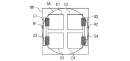
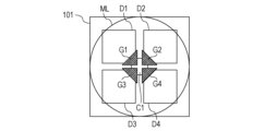
- FIGS. 16B and 16C show a configuration in which four photodiodes D1 to D4 are provided as four photoelectric conversion units for one microlens ML.
- a transfer transistor is provided corresponding to each of the photodiodes D1 to D4, and the gates G1 to G4 are gate electrodes of the corresponding transfer transistors.
- FIG. 16B gates G1, G3 transfer charge to pixel readout circuit R1.
- Gates G2 and G4 transfer charge to pixel readout circuit R2.
- Each of the pixel readout circuits R1 and R2 is provided with the capacitive element C1 shown in FIG.
- FIG. 16C is a form in which gates G1 to G4 are provided to transfer charges to one capacitive element C1. Even in such a form, the present embodiment can be suitably implemented.
- phase difference detection type focus detection can be performed by reading signals (focus detection signals) from some of the unit pixels 101 and some of the other unit pixels 101 . It is sufficient that at least some of the plurality of pixels provided in the pixel array have a configuration in which focus detection signals can be read out.
- the present embodiment has a configuration of the unit pixel 101 capable of phase difference detection.
- the AI processing section can further perform the focus detection operation.
- a detection unit 244 that performs focus detection may be provided on the second substrate 200 in addition to the AI processing unit.
- the arrangement of the second substrate of the detection section 244 is not particularly limited, but in the form of FIG. With respect to the AI processing unit and the detection unit 244 that generate heat, the temperature of the second substrate 200 can be easily made uniform by providing the detection unit 244 at a position away from the AI processing unit.
- FIG. 18 shows an example of the joining form of the first substrate 100 and the second substrate 200 of this embodiment.
- a first layer CFL is provided between the microlens ML and the first substrate 100 .
- An antireflection film, a color filter, and the like are provided on the first layer CFL.
- the first structure layer CFL may include a fixed charge film disposed on the first surface (incident surface) of the first substrate 100 .
- Photodiodes D1 and D2 are provided on the first substrate 100 .
- Gates G1 and G2 of transfer transistors are arranged on the second surface of the first substrate 100 .
- Gates of other transistors are also disposed on the second side of the first substrate 100 (not shown).
- the second structural layer L1 has a plurality of wiring layers and a plurality of interlayer insulating films. Wiring layers M1 and M2 are shown as a plurality of wiring layers.
- the second structural layer L1 has a first conductive portion MB11. The first conductive portion MB11 is connected to the wiring layer M2 by a plurality of interlayer connection portions TH1 and TH2.
- the third structural layer L2 also includes multiple wiring layers and multiple interlayer insulating films.
- a wiring layer M21 is shown as one of the plurality of wiring layers.
- the third structural layer L2 has a second conductive portion MB21. The contact between the first conductive portion MB11 and the second conductive portion MB21 results in electrical continuity.
- a bonding portion BD1 is formed by the first conductive portion MB11 and the second conductive portion MB21.
- An insulating film is formed on the surface on which the conductive portion MB11 is provided.
- An insulating film is formed on the surface on which the conductive portion MB21 is provided.
- the insulating film provided on the surface provided with the conductive portion MB11 and the insulating film provided on the surface provided with the conductive portion MB21 are bonded to each other. That is, at the bonding surface between the second structural layer L1 and the third structural layer L2, the bonding between the conductive portion MB11 and the conductive portion MB21, the insulating film included in the second structural layer L1, and the insulating film included in the third structural layer L2 are The junction is made by The insulating film included in the second structural layer L1 and the insulating film included in the third structural layer L2 are films containing silicon and oxygen.
- the second conductive portion MB21 is connected to the wiring layer M21 by a plurality of interlayer connection portions TH3 and TH4.
- the interlayer connection portions TH1, TH2, TH3, and TH4 may be made of a conductive material such as tungsten.
- the wiring layers M1, M2, and M21 may also be made of a conductive material, such as copper or aluminum.
- the first conductive portion MB11 and the second conductive portion MB21 forming the bonding portion BD1 may also be made of a conductive material, such as copper.
- a well region WEL is provided on the second substrate 200 .
- a gate SG of each transistor is arranged between the second substrate 200 and the wiring layer.
- FIG. 17 shows several junction structures ST1 to ST4.
- the structure ST1 including the bonding portion BD1 described above is a structure in which one electrical node is formed by one first conductive portion and one second conductive portion.
- Structures ST2-ST4 are structures in which one electrical node is formed by a plurality of junctions.
- one wiring included in the second structural layer L1 is connected to multiple junctions BD2 and BD3.
- one wiring included in the third structural layer L2 is connected to the joint BD2, and another wiring is connected to the joint BD3.
- one wiring included in the second structural layer L1 is connected to the junction BD4, and another wiring is connected to the junction BD5.
- one wiring included in the third structural layer L2 is connected to the junctions BD4 and BD5.
- one wiring included in the second structural layer L1 is connected to the junctions BD6 and BD7.
- one wiring included in the third structural layer L2 is connected to the junctions BD6 and BD7.
- These structures ST1 to ST4 can be used properly according to the location of the photoelectric conversion device and the signal (voltage) to be transmitted.
- one of the structures ST2 to ST4 is selected in order to reduce the resistance value of the transmission path.
- the path for transmitting a signal for each row or each column of the unit pixel 101 is restricted by the row pitch or the column pitch, so the structure ST1 is selected.
- the joints BD1 to BD7 and the connected wiring also act as heat radiation paths. Therefore, for a joint portion that overlaps an AI processed portion that generates a large amount of heat in a plan view, one of the structures ST2 to ST4 can be used to facilitate the release of heat generated in the AI processed portion.
- the structures ST3 and ST4 have one wiring between the second substrate 200 and a length connected to a plurality of joints. By providing a long wiring in the vicinity of the AI processing section that generates a large amount of heat, the heat can be released favorably.
- a plurality of interlayer connection portions TH1 to TH4 are connected to each of the first conductive portion MB11 and the second conductive portion MB21. This has the effect of facilitating heat release compared to the case where one interlayer connection is provided for each of the first conductive portion MB11 and the second conductive portion MB21.
- one of the structures ST2 to ST4 is used for a joint portion that overlaps an AI processing portion that generates a large amount of heat in a plan view.
- the other joint maintains electrical continuity. be able to.
- a plurality of photodiodes D1 and D2 are provided for one microlens, but one photodiode shown in FIG. 2 may be provided. Also, a phase difference detection type focus detection signal may be generated by shielding part of this one photodiode.
- the items described in this embodiment, including the configuration of FIG. 18, can be implemented in combination with the following embodiments. For example, the configurations shown in FIGS. 15 and 16A-16C can be applied to all of the following embodiments.
- FIG. 4 shows a configuration example of the second substrate 210 of the photoelectric conversion device according to this embodiment. Note that the AI processing units 203c and 203d are the same as those of the first embodiment, so description thereof is omitted.
- the AI processing units 203c and 203d have the same configuration and are arranged symmetrically at the left and right ends of the second substrate 210. As shown in FIG.
- FIG. 5 is an enlarged view of the dashed line part in FIG. n
- AI processing circuits 204 having the same function are arranged inside the AI processing unit 203d, and each AI processing circuit is electrically directly connected to the preprocessing units 202b and 202d.
- the preprocessing unit 202b and AI processing circuits 1, 2, 3, and 4 are connected, and the preprocessing unit 202d, AI processing circuit 5, and AI processing circuit n are directly connected.
- the number of AI processing circuits included in the AI processing units is greater than the number of preprocessing circuits 202 provided on the second substrate 200 . Thereby, the heat generated by the machine learning process can be more preferably reduced.
- the heat generated in the second substrate 210 can be dispersed by further dispersing the signal processing units that perform processing based on the neural network calculation model. This can reduce the influence of the heat generated on the second substrate 200 side on the pixel array 100 of the first substrate 100 .
- processing speed can be increased by performing processing based on the neural network calculation model in parallel using multiple AI processing circuits.
- FIG. 6 is an enlarged view of the dashed line portion of FIG. 4 in the second embodiment.
- the AI processing unit 203e shown in FIG. 6 is provided as the AI processing unit 203d shown in FIG.
- the same configuration as the AI processing unit 203e shown in FIG. 6 is also provided in the AI processing unit 203c shown in FIG. Note that the configuration other than the AI processing unit 203e is the same as in the first and second embodiments, so the description is omitted.
- AI processing circuits having a fixed circuit configuration capable of executing stepwise data processing are arranged, and each of the AI processing circuits 205(1) to 205(n) are electrically connected in series.
- the image data converted by the preprocessing unit is passed to the AI processing circuit 205(1), the AI processing circuit 205(2), and the AI processing circuit 205(3) in this order.
- a process based on is executed.
- the AI processing circuit 205(1) is electrically directly connected to the preprocessing section 202b, and the AI processing circuit 205(n) is electrically connected to the preprocessing section 202d.
- FIG. 7 is a timing chart schematically showing calculation operations based on the neural network calculation model performed by the AI processing circuit in this embodiment. From time t1 to t2, the AI processing circuit 205(1) performs processing based on the neural network calculation model on the image data (hereinafter referred to as image data c) converted by the preprocessing unit 202b. This image data c is based on the digital data output from the AD conversion circuit 201c.
- image data c is based on the digital data output from the AD conversion circuit 201c.
- the AI processing circuit 205(1) performs processing based on the neural network calculation model on the image data (hereinafter referred to as image data d) converted by the preprocessing unit 202b. Execute. This image data d is based on the digital data output from the AD conversion circuit 201d.
- the image data c is processed by the AI processing circuit 205(1) from time t1 to t2. Also, the image data c is processed by another AI processing circuit 205(2) from time t2 to t3.
- AI processing circuits 205(1) and (2) have different neural network calculation models. Therefore, AI processing circuit 205(2) performs processing based on a neural network calculation model different from the processing performed by AI processing circuit 205(1).
- the AI processing circuit 205(2) performs processing on the image data d based on a neural network calculation model different from the processing performed by the AI processing circuit 205(1). Also, the AI processing circuit 205(3) performs processing on the image data c based on a neural network calculation model different from the processing performed by the AI processing circuit 205(2).
- the AI processing circuit 205(3) performs processing on the image data d based on a neural network calculation model different from the processing performed by the AI processing circuit 205(2).
- the image data converted by the preprocessing unit 202d based on the digital data output from the AD conversion circuit 201g is denoted as image data d.
- image data converted by the signal processing circuit 202d based on the digital data output from the AD conversion circuit 201h is referred to as image data h.
- the AI processing circuit 205(n-2), the AI processing circuit 205(n-1), and the AI processing circuit 205(n) are processed from time t4 to t5, respectively. Processing based on different neural network computational models is performed sequentially. This processing is as shown in FIG.
- the AI processing unit of the photoelectric conversion device in this embodiment has a multi-stage pipeline configuration consisting of three stages, and executes processing based on a neural network calculation model in a sequential processing method.
- the layout of the AI processing circuits described in this embodiment is only an example, and it is desirable that the connection method of each AI processing circuit be appropriately laid out according to the amount of heat generated by each AI processing circuit and the number of stages of processing.
- the AI processing circuits are arranged in series from the upper and lower ends of the second substrate toward the center of the second substrate in a plan view viewed from above the second substrate. It is not limited to this example, and may be arranged in series from the center of the second substrate 200 toward the upper end and the lower end.
- the AI processing circuit connected to the preprocessing unit 202b may be arranged on the upper end of the second substrate
- the AI processing circuit connected to the preprocessing unit 202d may be arranged in the center of the second substrate.
- the direction of delivery of the image data converted by the preprocessing unit is the direction from the upper end side to the lower end side when viewed from the upper surface of the second substrate.
- heat generated in the second substrate 210 can be dispersed by further dispersing the processing units that perform processing based on the neural network calculation model. Therefore, the influence of the heat generated on the second substrate side on the pixel array 100 of the first substrate 100 can be reduced.
- the processing speed can be increased by performing processing based on the neural network calculation model in parallel using multiple AI processing circuits.
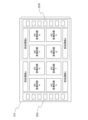
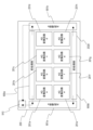
- FIG. 8 is a diagram showing the configuration of the second substrate 400 in this embodiment.
- the photoelectric conversion device according to the present embodiment has a configuration in which one AD converter 401 is provided on the second substrate 400 for one unit pixel 101 on the first substrate 100 . Thereby, analog signals output from all the unit pixels 101 can be collectively converted into digital data at the same time by the respective AD converters.
- 402a to 402d shown in FIG. 8 are preprocessing and AI processing units, respectively, which convert the digital data converted by the AD converter 401 into image data. Furthermore, processing based on a neural network calculation model is performed on the converted image data.
- the circuit regions for performing this preprocessing and AI processing are shown as 402a-d in FIG.
- the preprocessing unit and AI processing units 402a to 402d are a first signal processing unit, a second signal processing unit, a third signal processing unit, and a fourth signal processing unit, respectively.
- pads 800 for inputting signals (including power supply voltage) from the outside of the photoelectric conversion device or for outputting signals to the outside of the photoelectric conversion device are provided on four sides of the second substrate 200.
- a plurality of AI processing units are located in an area between the outer periphery provided with pads on four sides and the AD conversion unit (an area formed by the AD converters 401 provided over multiple rows and multiple columns). is provided.
- the pads 800 are provided on all four sides of the second substrate 200 in FIG. 8, they may be provided on two opposing sides.
- the digital data output from the AD converter 401 is input to either the preprocessing unit or the AI processing units 402a to 402d depending on the position where the AD converter 401 is arranged on the second substrate 400.
- the elements that execute processing based on the neural network calculation model are arranged, and they are arranged at approximately equal intervals.
- the heat generated in the second substrate 400 by the AI processing section can be dispersed. Therefore, the influence of the heat generated on the second substrate side on the pixel array of the first substrate 100 can be reduced.
- processing based on a neural network calculation model can be performed in parallel using a plurality of AI processing units, making it possible to increase the processing speed.
- the AI processing unit described in this embodiment may have a circuit configuration that executes stepwise data processing as described in the third embodiment. That is, each AI processing circuit may be electrically connected in series, have a multistage pipeline configuration, and execute processing based on a neural network calculation model in a sequential processing method.
- the AI processing circuits in the preprocessing units and AI processing units 402a to 402d have a circuit configuration capable of performing stepwise data processing. connected in series.
- the preprocessing unit and the AI processing units 402a, 402b, 402c, and 403d may be connected so as to circle the second substrate 400, or only some of the AI processing units 402a to 402d may be connected.
- the AI processing units 402a and 402b are connected, the AI processing units 402c and 402d are connected. Then, the AI processing units 402a and 402b, and the AI processing units 402c and 402d perform sequential processing. The sequential processing of the AI processing units 402a and 402b, and the AI processing units 402c and 402d may be performed in parallel at the same time.
- different AI processing units perform signal processing for each frame.
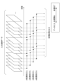
- FIG. 9 is a diagram showing the configuration of the second substrate 200 of this embodiment.
- the preprocessing unit 900a outputs the same data to both AI processing units 901a and 901b. Also, the preprocessing unit 900b outputs the same data to both the AI processing units 901a and 901b. That is, the AI processing units 901a and 901b receive the same data from the plurality of preprocessing units 900a and 900b. Various parameters of the AI processing units 901a and 901b are adjusted by machine learning, but the parameters are different between the AI processing units 901a and 901b. Therefore, even when the same data is input to the AI processing units 901a and 901b, the output results of the AI processing units 901a and 901b may differ.
- the output results of the AI processing units 901 a and 901 b are input to the integration processing unit 910 .
- the integration processing unit 910 performs one of the following operations when the output results of the AI processing units 901a and 901b are different. (1) Among the output results of the AI processing units 901a and 901b, a highly reliable output result is selected and output to the outside of the photoelectric conversion device. Select and output the corresponding result from the lookup table for the combination of the output results of 901a and 901b. output more information
- the determination of the reliability in (1) may be performed by referring to the output result of the AI processing unit 901 in the past. You can give Alternatively, each of the AI processing units 901a and 901b may output reliability information for the output result, and the one with the higher reliability information may be selected.
- the reliability information of (3) can cause each of the AI processing units 901a and 901b to output reliability information for the output result, and output the reliability information to the outside of the photoelectric conversion device.
- a plurality of AI processing units 901 perform signal processing involving machine learning processing on the same data. Thereby, the accuracy of the processing result output by the AI processing unit can be improved.
- the photoelectric conversion device of this embodiment can have redundancy in the AI processing unit.
- one of the AI processing units 901a and 901b may fail or the signal accuracy may be significantly degraded.
- the operation of the one AI processing unit can be stopped, or the output result can be ignored, and the output result of the other AI processing unit can be adopted.
- the operation of the photoelectric conversion device can be continued even if some of the AI processing units fail or the signal accuracy is degraded.
- the configuration of the photoelectric conversion device of this embodiment can be the same as that of the fifth embodiment, but can be configured with more AI processing units as shown in FIG. The following description is based on the configuration of FIG.
- each of the AD conversion circuits a to h can selectively output digital data to either one of the preprocessing units 900a and 900b, as shown for the AD conversion circuit a.
- each of the AD conversion circuits a to h may further include a configuration capable of outputting digital data in parallel with both the preprocessing units 900a and 900b.
- FIG. 11 is a diagram showing the operation of the AI processing unit of this embodiment.
- image data image data corresponding to one screen output of the AD conversion units 921a to 921h of each frame is shown.
- the AI processing unit 921a starts processing image data for n frames (n is a natural number). After that, while the AI processing unit 921a is processing the image data, another AI processing unit 921b starts processing the n+1 frame of image data. Similarly, while the AI processing units 921a and 921b are processing image data, the AI processing unit 921c starts processing n+3 frame image data. Similarly, while the AI processing units 921a, 921b, and 921c are processing image data, the AI processing unit 921d starts processing n+4 frame image data.
- the AI processing unit 921a finishes processing the image data and starts processing the n+5 frame image data again. Similar operations are repeated thereafter.
- the preprocessing unit 900a can selectively output digital data to the AI processing units 921a and 921b, so that the multiple frames of image data can be distributed frame by frame to the multiple AI processing units.
- AD conversion circuits a to h further include a configuration capable of selectively outputting digital data to either one of preprocessing units 900a and 900b. It facilitates the allocation of the AI processing part of
- the AD conversion circuits a to h are configured to selectively output digital data to either one of the preprocessing units 900a and 900b.
- the preprocessing units 900a and 900b may be made into one preprocessing unit 900, and this one preprocessing unit 900 may be distributed to the four AI processing units 921a to 921d.
- the number of AI processing units 921 is not limited to four, and may be two or more.
- the learned models held by the AI processing units 921a to 921d can be the same. As a result, even if different AI processing units 921 perform processing for each frame, it is possible to obtain an output result with the same level of reliability accuracy.
- each of the plurality of AI processing units 921a to 921d independently performs machine learning. This machine learning may or may not use teacher data.
- the AI processing units 921a to 921d After the AI processing units 921a to 921d complete machine learning, they input a signal whose expected output result is known to the photoelectric conversion device. For example, assuming that "the subject is a human face" as an expected output result, an example in which a photoelectric conversion device is caused to image a human face will be described.
- the integration processing unit 910 receives the output results of the AI processing units 921a to 921d.
- the integrated processing unit 910 increases the reliability of the AI processing unit 921 that outputs the correct output result (“the subject is a human face”) among the AI processing units 921a to 921d.
- the photoelectric conversion device repeats the operation of comparing the expected output result and the actual output result of the AI processing unit 921 .
- the integrated processing unit 910 identifies the AI processing unit 921 that is likely to output correct output results among the AI processing units 921a to 921d.
- the integrated processing unit 910 applies the learned model of the identified AI processing unit 921 to the other AI processing units 921 .
- the AI processing units 921a to 921d can have a common trained model with high reliability.
- the configuration of the photoelectric conversion device of this embodiment can be the same as that of the sixth embodiment.
- the integrated processing unit 910 outputs the processing results to the outside of the photoelectric conversion device based on the output results of the multiple frames output by the multiple AI processing units.
- FIG. 12 is a diagram showing operations of the AI processing units 921a to 921d shown in FIG. 10 in this embodiment. The difference from the operation shown in FIG. 11 is that the integrated processing unit 910 performs comprehensive judgment from the output results of the plurality of AI processing units 921a to 921d and outputs the processing result to the outside of the photoelectric conversion device.
- the most output result among the output results of the plurality of AI processing units 921a to 921d is adopted and output.
- the plurality of AI processing units 921a to 921d may have the same learned model as described in the sixth embodiment.
- the plurality of AI processing units 921a to 921d may have different trained models.
- a signal whose expected output result is known is input to the photoelectric conversion device.
- the integration processing unit 910 receives the output results of the AI processing units 921a to 921d. It is assumed that some AI processing units output an output result that "the subject is a human face” and other AI processing units output an output result other than "the subject is a human face”.
- the integrated processing unit 910 increases the reliability of the AI processing unit 921 that outputs the correct output result (“the subject is a human face”) among the AI processing units 921a to 921d.
- the photoelectric conversion device repeats the operation of comparing the expected output result and the actual output result of the AI processing unit 921 .
- the integrated processing unit 910 determines the reliability of each of the AI processing units 921a to 921d.
- the integration processing unit 910 assigns reliability parameters to the output results of the plurality of AI processing units 921a to 921d, and determines the processing results to be output to the outside of the photoelectric conversion device.
- each of the plurality of AI processing units 921a to 921d processes image data of different frames.
- image data of the same frame may be processed by a plurality of AI processing units 921a to 921d.
- the integrated processing unit 910 may perform comprehensive determination as described in the present embodiment, and output the processing result to the outside of the photoelectric conversion device.
- FIG. 14 shows the projection positions of the pixel array section 110 provided on the first substrate on the second substrate when viewed from above.
- the AI processing units 203a and 203b are provided at positions that do not overlap with the pixel array unit 110 in plan view.
- the pixel array section 110 is less susceptible to heat generation from the AI processing section.
- the preprocessing units 202a to 202d are also provided at positions that do not overlap with the pixel array unit 110 in plan view. As a result, the pixel array section 110 is less likely to be affected by heat generated in the preprocessing sections 202a to 202d.
- the operation processing speed may be made different for a plurality of AI processing units.
- the AI processing unit with the faster operation processing speed may be set further away from the pixel array position in plan view than the AI processing unit with the lower operation processing speed.
- the AI processing unit having a high operation processing speed also generates a large amount of heat, it is possible to reduce the influence of the heat generated by the AI processing unit on the pixel array unit.
- the AI processing section may be provided on the first substrate.
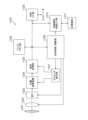
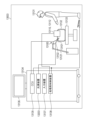
- FIG. 19 is a block diagram showing the configuration of a photoelectric conversion system 11200 according to this embodiment.
- a photoelectric conversion system 11200 of this embodiment includes a photoelectric conversion device 11204 .
- any of the photoelectric conversion devices described in the above embodiments can be applied to the photoelectric conversion device 11204 .
- the photoelectric conversion system 11200 can be used, for example, as an imaging system. Specific examples of imaging systems include digital still cameras, digital camcorders, surveillance cameras, network cameras, and the like.
- FIG. 19 shows an example of a digital still camera as the photoelectric conversion system 11200 .
- a photoelectric conversion system 11200 shown in FIG. 19 has a photoelectric conversion device 11204 and a lens 11202 that forms an optical image of a subject on the photoelectric conversion device 11204 .
- the photoelectric conversion system 11200 also has an aperture 11203 for varying the amount of light passing through the lens 11202 and a barrier 11201 for protecting the lens 11202 .
- a lens 11202 and a diaphragm 11203 are an optical system for condensing light onto the photoelectric conversion device 11204 .
- the photoelectric conversion system 11200 has a signal processing unit 11205 that processes the output signal output from the photoelectric conversion device 11204 .
- the signal processing unit 11205 performs a signal processing operation of performing various corrections and compressions on an input signal and outputting the signal as necessary.
- the photoelectric conversion system 11200 further has a buffer memory section 11206 for temporarily storing image data, and an external interface section (external I/F section) 11209 for communicating with an external computer or the like.
- the photoelectric conversion system 11200 includes a recording medium 11211 such as a semiconductor memory for recording or reading image data, and a recording medium control interface section (recording medium control I/F section) for recording or reading the recording medium 11211. 11210.
- the recording medium 11211 may be built in the photoelectric conversion system 11200 or may be detachable. Communication from the recording medium control I/F unit 11210 to the recording medium 11211 and communication from the external I/F unit 11209 may be performed wirelessly.
- the photoelectric conversion system 11200 has an overall control/calculation unit 11208 that performs various calculations and controls the entire digital still camera, and a timing generation unit 11207 that outputs various timing signals to the photoelectric conversion device 11204 and the signal processing unit 11205 .
- a timing signal or the like may be input from the outside, and the photoelectric conversion system 11200 may include at least a photoelectric conversion device 11204 and a signal processing unit 11205 that processes an output signal output from the photoelectric conversion device 11204. good.
- the overall control/arithmetic unit 11208 and the timing generation unit 11207 may be configured to implement some or all of the control functions of the photoelectric conversion device 11204 .
- the photoelectric conversion device 11204 outputs the image signal to the signal processing unit 11205 .
- a signal processing unit 11205 performs predetermined signal processing on the image signal output from the photoelectric conversion device 11204 and outputs image data. Also, the signal processing unit 11205 generates an image using the image signal. Also, the signal processing unit 11205 may perform ranging calculation on the signal output from the photoelectric conversion device 11204 .
- the signal processing unit 11205 and the timing generation unit 11207 may be mounted on the photoelectric conversion device. That is, the signal processing unit 11205 and the timing generation unit 11207 may be provided on the substrate on which the pixels are arranged, or may be provided on another substrate.
- FIG. 20 is a block diagram showing a configuration example of a distance image sensor, which is electronic equipment using the photoelectric conversion device described in the above embodiments.
- the distance image sensor 12401 comprises an optical system 12407, a photoelectric conversion device 12408, an image processing circuit 12404, a monitor 12405, and a memory 12406.
- the distance image sensor 12401 receives the light (modulated light or pulsed light) projected from the light source device 12409 toward the subject and reflected by the surface of the subject, thereby producing a distance image corresponding to the distance to the subject. can be obtained.
- the optical system 12407 includes one or more lenses, guides image light (incident light) from a subject to the photoelectric conversion device 12408, and forms an image on the light receiving surface (sensor portion) of the photoelectric conversion device 12408.
- the photoelectric conversion device of each embodiment described above is applied as the photoelectric conversion device 12408 , and a distance signal indicating the distance obtained from the received light signal output from the photoelectric conversion device 12408 is supplied to the image processing circuit 12404 .
- the image processing circuit 12404 performs image processing to construct a distance image based on the distance signal supplied from the photoelectric conversion device 12408 .
- a distance image (image data) obtained by the image processing is supplied to the monitor 12405 to be displayed, or supplied to the memory 406 to be stored (recorded).
- the range image sensor 12401 configured in this way, by applying the above-described photoelectric conversion device, it is possible to obtain, for example, a more accurate range image as the characteristics of the pixels are improved.
- the technology (the present technology) according to the present disclosure can be applied to various products.
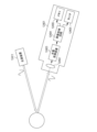
- the technology according to the present disclosure may be applied to an endoscopic surgery system.
- FIG. 21 is a diagram showing an example of a schematic configuration of an endoscopic surgery system to which the technology according to the present disclosure (this technology) can be applied.
- FIG. 21 shows how an operator (physician) 13131 is performing surgery on a patient 13132 on a patient bed 13133 using an endoscopic surgery system 13003 .
- the endoscopic surgery system 13003 is composed of an endoscope 13100, a surgical tool 13110, and a cart 13134 on which various devices for endoscopic surgery are mounted.
- An endoscope 13100 is composed of a lens barrel 13101 having a predetermined length from its distal end inserted into the body cavity of a patient 13132 and a camera head 13102 connected to the proximal end of the lens barrel 13101 .
- an endoscope 13100 configured as a so-called rigid scope having a rigid lens barrel 13101 is illustrated, but the endoscope 13100 may be configured as a so-called flexible scope having a flexible lens barrel. good.
- the tip of the lens barrel 13101 is provided with an opening into which the objective lens is fitted.
- a light source device 13203 is connected to the endoscope 13100 , and light generated by the light source device 13203 is guided to the tip of the lens barrel 13101 by a light guide extending inside the lens barrel 13101 . This light is directed through an objective lens toward an object of observation within the body cavity of the patient 13132 .
- the endoscope 13100 may be a straight scope, a perspective scope, or a side scope.
- An optical system and a photoelectric conversion device are provided inside the camera head 13102, and the reflected light (observation light) from the observation target is focused on the photoelectric conversion device by the optical system.
- the photoelectric conversion device photoelectrically converts the observation light to generate an electrical signal corresponding to the observation light, that is, an image signal corresponding to the observation image.
- the photoelectric conversion device the photoelectric conversion device described in each of the above embodiments can be used.
- the image signal is transmitted to a camera control unit (CCU: Camera Control Unit) 13135 as RAW data.
- CCU Camera Control Unit
- the CCU 13135 is composed of a CPU (Central Processing Unit), a GPU (Graphics Processing Unit), etc., and controls the operations of the endoscope 13100 and the display device 13136 in an integrated manner. Further, the CCU 13135 receives an image signal from the camera head 13102 and performs various image processing such as development processing (demosaicing) for displaying an image based on the image signal.
- image processing such as development processing (demosaicing) for displaying an image based on the image signal.
- the display device 13136 displays an image based on the image signal subjected to image processing by the CCU 13135 under the control of the CCU 13135 .
- the light source device 13203 is composed of, for example, a light source such as an LED (Light Emitting Diode), and supplies the endoscope 13100 with irradiation light for photographing a surgical site or the like.
- a light source such as an LED (Light Emitting Diode)
- LED Light Emitting Diode
- the input device 13137 is an input interface for the endoscopic surgery system 13003.
- the user can input various information and instructions to the endoscopic surgery system 13003 via the input device 13137 .
- the treatment instrument control device 13138 controls driving of the energy treatment instrument 13112 for tissue cauterization, incision, or blood vessel sealing.
- the light source device 13203 that supplies irradiation light to the endoscope 13100 for photographing the surgical site can be composed of, for example, a white light source composed of an LED, a laser light source, or a combination thereof.
- a white light source is configured by combining RGB laser light sources, the output intensity and output timing of each color (each wavelength) can be controlled with high accuracy. It can be carried out.
- the object to be observed is irradiated with laser light from each of the RGB laser light sources in a time division manner, and by controlling the drive of the imaging element of the camera head 13102 in synchronization with the irradiation timing, each of RGB can be handled. It is also possible to pick up images by time division. According to this method, a color image can be obtained without providing a color filter in the imaging element.
- the driving of the light source device 13203 may be controlled so as to change the intensity of the output light every predetermined time.
- the drive of the imaging device of the camera head 13102 in synchronism with the timing of the change in the intensity of the light to obtain images in a time-division manner and synthesizing the images, a high dynamic A range of images can be generated.
- the light source device 13203 may be configured to be capable of supplying light in a predetermined wavelength band corresponding to special light observation.
- Special light observation for example, utilizes the wavelength dependence of light absorption in body tissues. Specifically, a predetermined tissue such as a blood vessel on the surface of the mucous membrane is imaged with high contrast by irradiating light with a narrower band than the irradiation light (that is, white light) used during normal observation.
- irradiation light that is, white light
- fluorescence observation may be performed in which an image is obtained from fluorescence generated by irradiation with excitation light.
- body tissue is irradiated with excitation light and fluorescence from the body tissue is observed, or a reagent such as indocyanine green (ICG) is locally injected into the body tissue and the fluorescence wavelength of the reagent is observed in the body tissue. It is possible to obtain a fluorescent image by irradiating excitation light corresponding to .
- the light source device 13203 can be configured to supply narrowband light and/or excitation light corresponding to such special light observation.
- FIGS. 22A and 22B are schematic diagrams showing configuration examples of a photoelectric conversion system and a moving object according to this embodiment.
- an example of an in-vehicle camera is shown as a photoelectric conversion system.
- FIGs. 22A and 22B show an example of a vehicle system and a photoelectric conversion system mounted therein for imaging.
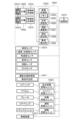
- a photoelectric conversion system 14301 includes a photoelectric conversion device 14302 , an image preprocessing unit 14315 , an integrated circuit 14303 and an optical system 14314 .
- the optical system 14314 forms an optical image of a subject on the photoelectric conversion device 14302 .
- the photoelectric conversion device 14302 converts the optical image of the object formed by the optical system 14314 into an electrical signal.
- the photoelectric conversion device 14302 is the photoelectric conversion device according to any one of the embodiments described above.
- An image preprocessing unit 14315 performs predetermined signal processing on the signal output from the photoelectric conversion device 14302 .
- the function of the image preprocessing unit 14315 may be incorporated within the photoelectric conversion device 14302 .
- the photoelectric conversion system 14301 is provided with at least two sets of an optical system 14314, a photoelectric conversion device 14302, and an image preprocessing unit 14315, and the output from each set of image preprocessing units 14315 is input to an integrated circuit 14303. It's like
- the integrated circuit 14303 is an integrated circuit for use in imaging systems, and includes an image processing unit 14304 including a memory 14305, an optical distance measurement unit 14306, a distance calculation unit 14307, an object recognition unit 14308, and an abnormality detection unit 14309.
- An image processing unit 14304 performs image processing such as development processing and defect correction on the output signal of the image preprocessing unit 14315 .
- the memory 14305 temporarily stores captured images and stores defect positions of captured pixels.
- An optical distance measuring unit 14306 performs focusing of a subject and distance measurement.
- a ranging calculation unit 14307 calculates ranging information from a plurality of image data acquired by a plurality of photoelectric conversion devices 14302 .
- the object recognition unit 14308 recognizes subjects such as cars, roads, signs, and people.
- the abnormality detection unit 14309 detects an abnormality in the photoelectric conversion device 14302, the abnormality detection unit 14309 notifies the main control unit 14313 of the abnormality.
- the integrated circuit 14303 may be realized by specially designed hardware, software modules, or a combination thereof. Also, it may be realized by FPGA (Field Programmable Gate Array), ASIC (Application Specific Integrated Circuit), etc., or by a combination thereof.
- FPGA Field Programmable Gate Array
- ASIC Application Specific Integrated Circuit
- the main control unit 14313 integrates and controls the operations of the photoelectric conversion system 14301, the vehicle sensor 14310, the control unit 14320, and the like. There is also a method in which the photoelectric conversion system 14301, the vehicle sensor 14310, and the control unit 14320 have individual communication interfaces without the main control unit 14313, and each of them transmits and receives control signals via a communication network (for example, CAN standard).
- a communication network for example, CAN standard
- the integrated circuit 14303 has a function of receiving a control signal from the main control unit 14313 or transmitting a control signal and setting values to the photoelectric conversion device 14302 by its own control unit.
- the photoelectric conversion system 14301 is connected to a vehicle sensor 14310, and can detect the running state of the own vehicle such as vehicle speed, yaw rate, and steering angle, the environment outside the own vehicle, and the state of other vehicles and obstacles.
- the vehicle sensor 14310 also serves as distance information acquisition means for acquiring distance information to an object.
- the photoelectric conversion system 14301 is also connected to a driving support control unit 1311 that performs various driving support functions such as automatic steering, automatic cruise, and anti-collision functions.
- the collision determination function based on the detection results of the photoelectric conversion system 14301 and the vehicle sensor 14310, it is possible to estimate a collision with another vehicle/obstacle and determine whether or not there is a collision. As a result, avoidance control when a collision is presumed and safety device activation at the time of collision are performed.
- the photoelectric conversion system 14301 is also connected to an alarm device 14312 that issues an alarm to the driver based on the judgment result of the collision judgment section. For example, when the collision possibility is high as a result of the judgment by the collision judging section, the main control section 14313 controls the vehicle to avoid collision and reduce damage by applying the brake, releasing the accelerator, or suppressing the engine output. conduct.
- the alarm device 14312 warns the user by sounding an alarm such as sound, displaying alarm information on a display unit screen of a car navigation system or a meter panel, or vibrating a seat belt or steering wheel.
- the photoelectric conversion system 14301 photographs the surroundings of the vehicle, for example, the front or rear.
- FIG. 22B shows an arrangement example of the photoelectric conversion system 14301 when the photoelectric conversion system 14301 captures an image in front of the vehicle.
- the two photoelectric conversion devices 14302 are arranged in front of the vehicle 14300 .
- the center line of the vehicle 14300 with respect to the forward/retreat azimuth or outer shape (for example, vehicle width) is regarded as a symmetrical axis
- the two photoelectric conversion devices 1302 are arranged line-symmetrically with respect to the symmetrical axis.
- This form is preferable for obtaining information on the distance between the vehicle 14300 and the object to be photographed and for determining the possibility of collision.
- the photoelectric conversion device 14302 is preferably arranged so as not to block the driver's field of view when the driver visually recognizes the situation outside the vehicle 14300 from the driver's seat. It is preferable that the warning device 14312 be arranged so as to be easily visible to the driver.
- the control that does not collide with another vehicle has been described, but it is also applicable to control that automatically drives following another vehicle, control that automatically drives so as not to stray from the lane, and the like.
- the photoelectric conversion system 14301 can be applied not only to a vehicle such as a vehicle, but also to a moving object (moving device) such as a ship, an aircraft, or an industrial robot.
- the present invention can be applied not only to mobile objects but also to devices that widely use object recognition, such as intelligent transportation systems (ITS).
- ITS intelligent transportation systems
- the photoelectric conversion device of the present invention may further have a configuration capable of acquiring various information such as distance information.
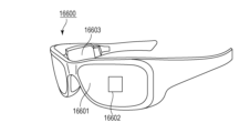
- FIG. 23A and 23B illustrate eyeglasses 16600 (smart glasses) according to one application.
- Glasses 16600 have a photoelectric conversion device 16602 .
- the photoelectric conversion device 16602 is the photoelectric conversion device described in each of the above embodiments.
- a display device including a light-emitting device such as an OLED or an LED may be provided on the rear surface side of the lens 16601 .
- One or more photoelectric conversion devices 16602 may be provided. Further, a plurality of types of photoelectric conversion devices may be used in combination.
- the arrangement position of the photoelectric conversion device 16602 is not limited to that shown in FIG. 23A.
- the spectacles 16600 further include a control device 16603.
- the control device 16603 functions as a power source that supplies power to the photoelectric conversion device 16602 and the display device.
- the control device 16603 controls operations of the photoelectric conversion device 16602 and the display device.
- the lens 16601 is formed with an optical system for condensing light onto the photoelectric conversion device 16602 .
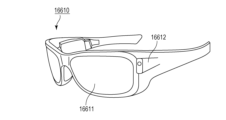
- FIG. 23B illustrates glasses 16610 (smart glasses) according to one application.
- the glasses 16610 have a control device 16612, and the control device 16612 is equipped with a photoelectric conversion device corresponding to the photoelectric conversion device 16602 and a display device.
- a photoelectric conversion device in the control device 16612 and an optical system for projecting light emitted from the display device are formed on the lens 16611 , and an image is projected onto the lens 16611 .
- the control device 16612 functions as a power source that supplies power to the photoelectric conversion device and the display device, and controls the operation of the photoelectric conversion device and the display device.
- the control device may have a line-of-sight detection unit that detects the line of sight of the wearer.
- Infrared rays may be used for line-of-sight detection.
- the infrared light emitting section emits infrared light to the eyeballs of the user who is gazing at the display image.
- a captured image of the eyeball is obtained by detecting reflected light of the emitted infrared light from the eyeball by an imaging unit having a light receiving element.
- the user's line of sight to the display image is detected from the captured image of the eyeball obtained by capturing infrared light.
- Any known method can be applied to line-of-sight detection using captured images of eyeballs.
- line-of-sight detection processing is performed based on the pupillary corneal reflection method.
- the user's line of sight is detected by calculating a line-of-sight vector representing the orientation (rotational angle) of the eyeball based on the pupil image and the Purkinje image included in the captured image of the eyeball using the pupillary corneal reflection method. be.
- the display device of the present embodiment may have a photoelectric conversion device having a light receiving element, and may control the display image of the display device based on the user's line-of-sight information from the photoelectric conversion device.
- the display device determines a first visual field area that the user gazes at and a second visual field area other than the first visual field area, based on the line-of-sight information.
- the first viewing area and the second viewing area may be determined by the control device of the display device, or may be determined by an external control device.
- the display resolution of the first viewing area may be controlled to be higher than the display resolution of the second viewing area. That is, the resolution of the second viewing area may be lower than that of the first viewing area.
- the display area has a first display area and a second display area different from the first display area. may be determined.
- the first viewing area and the second viewing area may be determined by the control device of the display device, or may be determined by an external control device.
- the resolution of areas with high priority may be controlled to be higher than the resolution of areas other than areas with high priority. In other words, the resolution of areas with relatively low priority may be lowered.
- AI may be used to determine the first field of view area and areas with high priority.
- the AI is a model configured to estimate the angle of the line of sight from the eyeball image and the distance to the object ahead of the line of sight, using the image of the eyeball and the direction in which the eyeball of the image was actually viewed as training data. It's okay.
- the AI program may be owned by the display device, the photoelectric conversion device, or the external device. If the external device has it, it is communicated to the display device via communication.
- Smart glasses can display captured external information in real time.
- the system of this embodiment will be described with reference to FIG.
- the present embodiment can be applied to a pathological diagnosis system in which a doctor or the like observes cells and tissues collected from a patient to diagnose a lesion, and a diagnosis support system that supports the system.
- the system of this embodiment may diagnose or assist in diagnosing lesions based on the acquired images.
- the system of this embodiment includes one or more pathology systems 15510. Furthermore, an analysis unit 15530 and a medical information system 15540 may be included.
- Each of the one or more pathology systems 15510 is a system mainly used by pathologists, and is installed in laboratories and hospitals, for example.
- Each pathology system 15510 may be installed in a different hospital, and is connected to the analysis unit 15530 and the medical information system 15540 via various networks such as wide area networks and local area networks.
- Each pathology system 15510 includes a microscope 15511, a server 15512, and a display device 15513.
- the microscope 15511 has the function of an optical microscope, takes an image of an observation object contained in a glass slide, and acquires a pathological image that is a digital image.
- Observation objects are, for example, tissues and cells collected from a patient, and may be pieces of flesh of organs, saliva, blood, and the like.
- the server 15512 stores and saves pathological images acquired by the microscope 15511 in a storage unit (not shown). Further, when receiving a viewing request, the server 15512 can search for pathological images held in a memory or the like and display the searched pathological images on the display device 15513 .
- the server 15512 and the display device 15513 may be connected via a display control device or the like.
- the observation target is a solid object such as a piece of flesh of an organ
- the observation target may be, for example, a stained slice.
- a sliced piece may be produced, for example, by slicing a block piece excised from a specimen such as an organ. Also, when slicing, the block pieces may be fixed with paraffin or the like.
- the microscope 15511 can include a low-resolution imaging unit for low-resolution imaging and a high-resolution imaging unit for high-resolution imaging.
- the low-resolution imaging section and the high-resolution imaging section may be different optical systems, or may be the same optical system. In the case of the same optical system, the resolution of the microscope 15511 may be changed according to the object to be imaged.
- the object to be observed is housed in a glass slide or the like and placed on a stage positioned within the angle of view of the microscope 15511.
- the microscope 15511 first acquires the entire image within the angle of view using the low-resolution imaging unit, and specifies the region of the observation object from the acquired entire image. Subsequently, the microscope 15511 divides the region where the observation target exists into a plurality of divided regions of a predetermined size, and sequentially captures each divided region with the high-resolution imaging unit, thereby acquiring a high-resolution image of each divided region. do.
- the stage may be moved, the imaging optical system may be moved, or both of them may be moved.
- each divided area may overlap adjacent divided areas in order to prevent occurrence of an imaging omission area due to unintended slippage of the glass slide.
- the whole image may contain identification information for associating the whole image with the patient. This identification information may be, for example, a character string, a QR code (registered trademark), or the like.
- the high-resolution image acquired by the microscope 15511 is input to the server 15512.
- Server 15512 can divide each high resolution image into smaller size sub-images. After generating the partial images in this way, the server 15512 executes a combining process for generating a single image by combining a predetermined number of adjacent partial images for all partial images. This compositing process can be repeated until finally one partial image is generated.
- a pyramid-structured partial image group is generated in which each layer is composed of one or more partial images.
- a partial image in a certain layer and a partial image in a different layer have the same number of pixels, but different resolutions. For example, when synthesizing a total of four partial images (2 ⁇ 2) to generate one partial image in the upper layer, the resolution of the partial image in the upper layer is half the resolution of the partial image in the lower layer used for synthesis. It has become.
- the generated partial image group of the pyramid structure can be stored, for example, in a memory or the like.
- the server 15512 receives a partial image acquisition request including identification information from another device (for example, the analysis unit 15530), the server 15512 transmits the partial image corresponding to the identification information to the other device.
- a partial image which is a pathological image, may be generated for each imaging condition such as focal length and staining condition.
- a specific pathological image and other pathological images corresponding to imaging conditions different from the specific imaging condition and having the same region as the specific pathological image are generated. They may be displayed side by side.
- Specific imaging conditions may be specified by the viewer. Further, when a plurality of imaging conditions are designated by the viewer, pathological images of the same region corresponding to each imaging condition may be displayed side by side.
- the server 15512 may store the pyramid structure partial image group in a storage device other than the server 15512, such as a cloud server. Furthermore, part or all of the partial image generation processing as described above may be executed by a cloud server or the like.
- a cloud server or the like.
- the medical information system 15540 is a so-called electronic medical record system, and stores information related to diagnosis, such as patient identification information, patient disease information, test information and image information used for diagnosis, diagnosis results, and prescription drugs.
- information related to diagnosis such as patient identification information, patient disease information, test information and image information used for diagnosis, diagnosis results, and prescription drugs.
- a pathological image obtained by imaging an observation target of a certain patient can be displayed on the display device 15514 after being temporarily stored via the server 15512 .
- a pathologist using the pathological system 15510 makes a pathological diagnosis based on the pathological image displayed on the display device 15513 .
- Pathological diagnosis results made by the pathologist are stored in the medical information system 15540 .
- the analysis unit 15530 can perform analysis on pathological images. A learning model created by machine learning can be used for this analysis.
- the analysis unit 15530 may derive a classification result of the specific region, a tissue identification result, or the like as the analysis result. Furthermore, the analysis unit 15530 may derive identification results such as cell information, number, position, brightness information, and scoring information for them. These pieces of information obtained by the analysis unit 15530 may be displayed on the display device 15513 of the pathology system 15510 as diagnosis support information.
- the analysis unit 15530 may be a server system configured with one or more servers (including cloud servers). Also, the analysis unit 15530 may be configured to be incorporated in, for example, the server 15512 within the pathological system 15510 . That is, various analyzes on pathological images may be performed within the pathological system 15510 .
- the photoelectric conversion device described in the above embodiments can be suitably applied to, for example, the microscope 15511 among the configurations described above. Specifically, it can be applied to a low-resolution imaging unit and/or a high-resolution imaging unit in the microscope 15511 . This makes it possible to reduce the size of the low-resolution imaging unit and/or the high-resolution imaging unit, or even downsize the microscope 15511 . As a result, transportation of the microscope 15511 is facilitated, and system introduction, system recombination, and the like can be facilitated.
- part or all of the processing from pathological image acquisition to pathological image analysis can be executed on the fly within the microscope 15511, so that the process can be performed more quickly. It is also possible to output accurate diagnostic support information.
- the configuration described above can be applied not only to diagnostic support systems, but also to general biological microscopes such as confocal microscopes, fluorescence microscopes, and video microscopes.
- the object to be observed may be a biological sample such as cultured cells, fertilized eggs, or sperm, a biological material such as a cell sheet or a three-dimensional cell tissue, or a living body such as a zebrafish or mouse.
- the object to be observed is not limited to a glass slide, and can be observed while stored in a well plate, petri dish, or the like.
- a moving image may be generated from a still image of an observation target acquired using a microscope.
- a moving image may be generated from still images captured continuously for a predetermined period of time, or an image sequence may be generated from still images captured at predetermined intervals.
- it is possible to observe the movements of cancer cells, nerve cells, myocardial tissue, sperm, etc. such as pulsation, elongation, and migration, and the division process of cultured cells and fertilized eggs. It becomes possible to analyze the dynamic features of objects using machine learning.
Landscapes
- Engineering & Computer Science (AREA)
- Multimedia (AREA)
- Signal Processing (AREA)
- Solid State Image Pick-Up Elements (AREA)
Priority Applications (3)
| Application Number | Priority Date | Filing Date | Title |
|---|---|---|---|
| JP2023572272A JPWO2023132002A1 (enExample) | 2022-01-05 | 2022-01-05 | |
| PCT/JP2022/000070 WO2023132002A1 (ja) | 2022-01-05 | 2022-01-05 | 光電変換装置、光電変換システム、移動体 |
| US18/759,615 US20240357258A1 (en) | 2022-01-05 | 2024-06-28 | Photoelectric conversion apparatus, photoelectric conversion system, and movable object |
Applications Claiming Priority (1)
| Application Number | Priority Date | Filing Date | Title |
|---|---|---|---|
| PCT/JP2022/000070 WO2023132002A1 (ja) | 2022-01-05 | 2022-01-05 | 光電変換装置、光電変換システム、移動体 |
Related Child Applications (1)
| Application Number | Title | Priority Date | Filing Date |
|---|---|---|---|
| US18/759,615 Continuation US20240357258A1 (en) | 2022-01-05 | 2024-06-28 | Photoelectric conversion apparatus, photoelectric conversion system, and movable object |
Publications (1)
| Publication Number | Publication Date |
|---|---|
| WO2023132002A1 true WO2023132002A1 (ja) | 2023-07-13 |
Family
ID=87073563
Family Applications (1)
| Application Number | Title | Priority Date | Filing Date |
|---|---|---|---|
| PCT/JP2022/000070 Ceased WO2023132002A1 (ja) | 2022-01-05 | 2022-01-05 | 光電変換装置、光電変換システム、移動体 |
Country Status (3)
| Country | Link |
|---|---|
| US (1) | US20240357258A1 (enExample) |
| JP (1) | JPWO2023132002A1 (enExample) |
| WO (1) | WO2023132002A1 (enExample) |
Citations (5)
| Publication number | Priority date | Publication date | Assignee | Title |
|---|---|---|---|---|
| JP2002165126A (ja) * | 2000-11-28 | 2002-06-07 | Canon Inc | 撮像装置及び撮像システム、並びに撮像方法 |
| JP2015216334A (ja) * | 2014-04-21 | 2015-12-03 | ソニー株式会社 | 固体撮像素子、固体撮像素子の製造方法、並びに、電子機器 |
| JP2018182038A (ja) * | 2017-04-12 | 2018-11-15 | ソニーセミコンダクタソリューションズ株式会社 | 固体撮像素子 |
| JP2020025263A (ja) * | 2018-07-31 | 2020-02-13 | ソニーセミコンダクタソリューションズ株式会社 | 積層型受光センサ及び電子機器 |
| WO2021161712A1 (ja) * | 2020-02-14 | 2021-08-19 | ソニーグループ株式会社 | 撮像装置及び車両制御システム |
Family Cites Families (8)
| Publication number | Priority date | Publication date | Assignee | Title |
|---|---|---|---|---|
| JP6341675B2 (ja) * | 2014-01-29 | 2018-06-13 | キヤノン株式会社 | 固体撮像装置及びその駆動方法並びにそれを用いた撮像システム |
| JP6704944B2 (ja) * | 2018-02-09 | 2020-06-03 | キヤノン株式会社 | 撮像装置、撮像システム、移動体 |
| JP2020098968A (ja) * | 2018-12-17 | 2020-06-25 | オリンパス株式会社 | 撮像素子、撮像装置、および撮像方法 |
| US10777611B1 (en) * | 2019-09-27 | 2020-09-15 | Sony Semiconductor Solutions Corporation | Image sensor |
| JP2021057825A (ja) * | 2019-09-30 | 2021-04-08 | キヤノン株式会社 | 信号処理装置及び方法、及び撮像装置 |
| KR102885349B1 (ko) * | 2019-11-05 | 2025-11-14 | 삼성전자주식회사 | 이미지 센서 |
| US11941519B2 (en) * | 2019-12-02 | 2024-03-26 | Waymo Llc | Machine learning training platform |
| JP7646380B2 (ja) * | 2021-02-04 | 2025-03-17 | キヤノン株式会社 | 光電変換装置、光電変換システム、移動体 |
-
2022
- 2022-01-05 JP JP2023572272A patent/JPWO2023132002A1/ja active Pending
- 2022-01-05 WO PCT/JP2022/000070 patent/WO2023132002A1/ja not_active Ceased
-
2024
- 2024-06-28 US US18/759,615 patent/US20240357258A1/en active Pending
Patent Citations (5)
| Publication number | Priority date | Publication date | Assignee | Title |
|---|---|---|---|---|
| JP2002165126A (ja) * | 2000-11-28 | 2002-06-07 | Canon Inc | 撮像装置及び撮像システム、並びに撮像方法 |
| JP2015216334A (ja) * | 2014-04-21 | 2015-12-03 | ソニー株式会社 | 固体撮像素子、固体撮像素子の製造方法、並びに、電子機器 |
| JP2018182038A (ja) * | 2017-04-12 | 2018-11-15 | ソニーセミコンダクタソリューションズ株式会社 | 固体撮像素子 |
| JP2020025263A (ja) * | 2018-07-31 | 2020-02-13 | ソニーセミコンダクタソリューションズ株式会社 | 積層型受光センサ及び電子機器 |
| WO2021161712A1 (ja) * | 2020-02-14 | 2021-08-19 | ソニーグループ株式会社 | 撮像装置及び車両制御システム |
Also Published As
| Publication number | Publication date |
|---|---|
| JPWO2023132002A1 (enExample) | 2023-07-13 |
| US20240357258A1 (en) | 2024-10-24 |
Similar Documents
| Publication | Publication Date | Title |
|---|---|---|
| CN112470462B (zh) | 层叠式光接收传感器和电子装置 | |
| JP7646380B2 (ja) | 光電変換装置、光電変換システム、移動体 | |
| US12183759B2 (en) | Photoelectric conversion apparatus, photoelectric conversion system, mobile body, and semiconductor substrate | |
| US20250343998A1 (en) | Photoelectric conversion apparatus | |
| US12368974B2 (en) | Photoelectric conversion device and photoelectric conversion system | |
| US20220246661A1 (en) | Photoelectric conversion apparatus, photoelectric conversion system, and mobile body | |
| JP7654415B2 (ja) | 光電変換装置、機器 | |
| JP7676158B2 (ja) | 光電変換装置、光電変換システム | |
| WO2023132002A1 (ja) | 光電変換装置、光電変換システム、移動体 | |
| US12243896B2 (en) | Photoelectric conversion apparatus, photoelectric conversion system, mobile body, and semiconductor substrate | |
| US12137291B2 (en) | Photoelectric conversion apparatus having pad arrangement | |
| US12028623B2 (en) | Photoelectric conversion apparatus, photoelectric conversion system, and semiconductor substrate | |
| US20250184636A1 (en) | Apparatus, system, and moving body | |
| JP2023174229A (ja) | 光電変換装置 |
Legal Events
| Date | Code | Title | Description |
|---|---|---|---|
| ENP | Entry into the national phase |
Ref document number: 2023572272 Country of ref document: JP Kind code of ref document: A |
|
| NENP | Non-entry into the national phase |
Ref country code: DE |
|
| 122 | Ep: pct application non-entry in european phase |
Ref document number: 22918594 Country of ref document: EP Kind code of ref document: A1 |