WO2023132002A1 - Photoelectric conversion device, photoelectric conversion system, and moving body - Google Patents
Photoelectric conversion device, photoelectric conversion system, and moving body Download PDFInfo
- Publication number
- WO2023132002A1 WO2023132002A1 PCT/JP2022/000070 JP2022000070W WO2023132002A1 WO 2023132002 A1 WO2023132002 A1 WO 2023132002A1 JP 2022000070 W JP2022000070 W JP 2022000070W WO 2023132002 A1 WO2023132002 A1 WO 2023132002A1
- Authority
- WO
- WIPO (PCT)
- Prior art keywords
- signal processing
- photoelectric conversion
- substrate
- conversion device
- processing
- Prior art date
Links
- 238000006243 chemical reaction Methods 0.000 title claims abstract description 232
- 238000012545 processing Methods 0.000 claims abstract description 392
- 239000000758 substrate Substances 0.000 claims abstract description 136
- 238000001514 detection method Methods 0.000 claims abstract description 34
- 238000010801 machine learning Methods 0.000 claims abstract description 19
- 238000007781 pre-processing Methods 0.000 claims description 57
- 239000010410 layer Substances 0.000 claims description 49
- 239000011229 interlayer Substances 0.000 claims description 9
- 239000004020 conductor Substances 0.000 claims description 5
- 238000010586 diagram Methods 0.000 description 39
- 238000003384 imaging method Methods 0.000 description 32
- 238000004364 calculation method Methods 0.000 description 28
- 238000013528 artificial neural network Methods 0.000 description 25
- 230000003287 optical effect Effects 0.000 description 23
- 230000000875 corresponding effect Effects 0.000 description 21
- 230000001575 pathological effect Effects 0.000 description 18
- 238000000034 method Methods 0.000 description 17
- 230000003321 amplification Effects 0.000 description 15
- 238000003199 nucleic acid amplification method Methods 0.000 description 15
- 238000004458 analytical method Methods 0.000 description 12
- 230000008569 process Effects 0.000 description 12
- 210000001519 tissue Anatomy 0.000 description 12
- 210000005252 bulbus oculi Anatomy 0.000 description 10
- 230000006870 function Effects 0.000 description 10
- 238000012546 transfer Methods 0.000 description 10
- 238000002674 endoscopic surgery Methods 0.000 description 8
- 238000005516 engineering process Methods 0.000 description 7
- 239000011521 glass Substances 0.000 description 7
- 230000020169 heat generation Effects 0.000 description 6
- 239000004065 semiconductor Substances 0.000 description 6
- 239000004984 smart glass Substances 0.000 description 6
- 230000005856 abnormality Effects 0.000 description 5
- 210000004027 cell Anatomy 0.000 description 5
- 238000004891 communication Methods 0.000 description 5
- 238000003745 diagnosis Methods 0.000 description 5
- 230000000694 effects Effects 0.000 description 5
- 210000003128 head Anatomy 0.000 description 5
- 230000010354 integration Effects 0.000 description 5
- 230000007170 pathology Effects 0.000 description 5
- 230000008859 change Effects 0.000 description 4
- 230000001276 controlling effect Effects 0.000 description 4
- 238000012937 correction Methods 0.000 description 4
- 230000005284 excitation Effects 0.000 description 4
- 230000000007 visual effect Effects 0.000 description 4
- 230000006866 deterioration Effects 0.000 description 3
- 238000009792 diffusion process Methods 0.000 description 3
- 238000007667 floating Methods 0.000 description 3
- 238000005259 measurement Methods 0.000 description 3
- 238000012986 modification Methods 0.000 description 3
- 230000004048 modification Effects 0.000 description 3
- 210000000056 organ Anatomy 0.000 description 3
- 238000010827 pathological analysis Methods 0.000 description 3
- 238000003672 processing method Methods 0.000 description 3
- RYGMFSIKBFXOCR-UHFFFAOYSA-N Copper Chemical compound [Cu] RYGMFSIKBFXOCR-UHFFFAOYSA-N 0.000 description 2
- 210000004204 blood vessel Anatomy 0.000 description 2
- 239000003153 chemical reaction reagent Substances 0.000 description 2
- 238000005094 computer simulation Methods 0.000 description 2
- 229910052802 copper Inorganic materials 0.000 description 2
- 239000010949 copper Substances 0.000 description 2
- 210000004748 cultured cell Anatomy 0.000 description 2
- 230000007547 defect Effects 0.000 description 2
- 238000011161 development Methods 0.000 description 2
- 235000013601 eggs Nutrition 0.000 description 2
- MOFVSTNWEDAEEK-UHFFFAOYSA-M indocyanine green Chemical compound [Na+].[O-]S(=O)(=O)CCCCN1C2=CC=C3C=CC=CC3=C2C(C)(C)C1=CC=CC=CC=CC1=[N+](CCCCS([O-])(=O)=O)C2=CC=C(C=CC=C3)C3=C2C1(C)C MOFVSTNWEDAEEK-UHFFFAOYSA-M 0.000 description 2
- 229960004657 indocyanine green Drugs 0.000 description 2
- 230000001678 irradiating effect Effects 0.000 description 2
- 230000003902 lesion Effects 0.000 description 2
- 230000001179 pupillary effect Effects 0.000 description 2
- 238000001028 reflection method Methods 0.000 description 2
- 230000002194 synthesizing effect Effects 0.000 description 2
- 241000252212 Danio rerio Species 0.000 description 1
- 206010028980 Neoplasm Diseases 0.000 description 1
- 230000004913 activation Effects 0.000 description 1
- 229910052782 aluminium Inorganic materials 0.000 description 1
- XAGFODPZIPBFFR-UHFFFAOYSA-N aluminium Chemical compound [Al] XAGFODPZIPBFFR-UHFFFAOYSA-N 0.000 description 1
- QVGXLLKOCUKJST-UHFFFAOYSA-N atomic oxygen Chemical compound [O] QVGXLLKOCUKJST-UHFFFAOYSA-N 0.000 description 1
- 230000004888 barrier function Effects 0.000 description 1
- 239000012620 biological material Substances 0.000 description 1
- 239000012472 biological sample Substances 0.000 description 1
- 230000005540 biological transmission Effects 0.000 description 1
- 230000015572 biosynthetic process Effects 0.000 description 1
- 210000004369 blood Anatomy 0.000 description 1
- 239000008280 blood Substances 0.000 description 1
- 201000011510 cancer Diseases 0.000 description 1
- 230000000295 complement effect Effects 0.000 description 1
- 238000007906 compression Methods 0.000 description 1
- 230000006835 compression Effects 0.000 description 1
- 210000004087 cornea Anatomy 0.000 description 1
- 230000002596 correlated effect Effects 0.000 description 1
- 230000006378 damage Effects 0.000 description 1
- 230000002950 deficient Effects 0.000 description 1
- 201000010099 disease Diseases 0.000 description 1
- 208000037265 diseases, disorders, signs and symptoms Diseases 0.000 description 1
- 238000010336 energy treatment Methods 0.000 description 1
- 238000005286 illumination Methods 0.000 description 1
- 238000010191 image analysis Methods 0.000 description 1
- 230000031700 light absorption Effects 0.000 description 1
- 229910052751 metal Inorganic materials 0.000 description 1
- 239000002184 metal Substances 0.000 description 1
- 238000013508 migration Methods 0.000 description 1
- 230000005012 migration Effects 0.000 description 1
- 210000004400 mucous membrane Anatomy 0.000 description 1
- 230000002107 myocardial effect Effects 0.000 description 1
- 210000002569 neuron Anatomy 0.000 description 1
- 229910052760 oxygen Inorganic materials 0.000 description 1
- 239000001301 oxygen Substances 0.000 description 1
- 239000012188 paraffin wax Substances 0.000 description 1
- 230000003071 parasitic effect Effects 0.000 description 1
- 239000000955 prescription drug Substances 0.000 description 1
- 230000010349 pulsation Effects 0.000 description 1
- 210000001747 pupil Anatomy 0.000 description 1
- 230000005855 radiation Effects 0.000 description 1
- 230000006798 recombination Effects 0.000 description 1
- 238000005215 recombination Methods 0.000 description 1
- 230000009467 reduction Effects 0.000 description 1
- 210000003296 saliva Anatomy 0.000 description 1
- 238000005070 sampling Methods 0.000 description 1
- 238000007789 sealing Methods 0.000 description 1
- 229910052710 silicon Inorganic materials 0.000 description 1
- 239000010703 silicon Substances 0.000 description 1
- 239000007787 solid Substances 0.000 description 1
- 238000010186 staining Methods 0.000 description 1
- 238000001356 surgical procedure Methods 0.000 description 1
- 238000003786 synthesis reaction Methods 0.000 description 1
- 238000012360 testing method Methods 0.000 description 1
- 238000012549 training Methods 0.000 description 1
- WFKWXMTUELFFGS-UHFFFAOYSA-N tungsten Chemical compound [W] WFKWXMTUELFFGS-UHFFFAOYSA-N 0.000 description 1
- 229910052721 tungsten Inorganic materials 0.000 description 1
- 239000010937 tungsten Substances 0.000 description 1
Images


Classifications
-
- H—ELECTRICITY
- H01—ELECTRIC ELEMENTS
- H01L—SEMICONDUCTOR DEVICES NOT COVERED BY CLASS H10
- H01L27/00—Devices consisting of a plurality of semiconductor or other solid-state components formed in or on a common substrate
- H01L27/14—Devices consisting of a plurality of semiconductor or other solid-state components formed in or on a common substrate including semiconductor components sensitive to infrared radiation, light, electromagnetic radiation of shorter wavelength or corpuscular radiation and specially adapted either for the conversion of the energy of such radiation into electrical energy or for the control of electrical energy by such radiation
- H01L27/144—Devices controlled by radiation
- H01L27/146—Imager structures
-
- H—ELECTRICITY
- H01—ELECTRIC ELEMENTS
- H01L—SEMICONDUCTOR DEVICES NOT COVERED BY CLASS H10
- H01L31/00—Semiconductor devices sensitive to infrared radiation, light, electromagnetic radiation of shorter wavelength or corpuscular radiation and specially adapted either for the conversion of the energy of such radiation into electrical energy or for the control of electrical energy by such radiation; Processes or apparatus specially adapted for the manufacture or treatment thereof or of parts thereof; Details thereof
- H01L31/08—Semiconductor devices sensitive to infrared radiation, light, electromagnetic radiation of shorter wavelength or corpuscular radiation and specially adapted either for the conversion of the energy of such radiation into electrical energy or for the control of electrical energy by such radiation; Processes or apparatus specially adapted for the manufacture or treatment thereof or of parts thereof; Details thereof in which radiation controls flow of current through the device, e.g. photoresistors
- H01L31/10—Semiconductor devices sensitive to infrared radiation, light, electromagnetic radiation of shorter wavelength or corpuscular radiation and specially adapted either for the conversion of the energy of such radiation into electrical energy or for the control of electrical energy by such radiation; Processes or apparatus specially adapted for the manufacture or treatment thereof or of parts thereof; Details thereof in which radiation controls flow of current through the device, e.g. photoresistors characterised by at least one potential-jump barrier or surface barrier, e.g. phototransistors
Definitions
- the present invention relates to a photoelectric conversion device, a photoelectric conversion system, and a moving object.
- a structure having a laminated structure in which multiple substrates are laminated is known.
- Patent Document 1 describes a laminated light receiving sensor in which a first substrate having pixels and a second substrate having a signal processing circuit (DSP) are laminated.
- the signal processing circuit executes processing based on a neural network calculation model.
- the processing signal processing circuit based on the neural network calculation model arranged on the second board consumes a large amount of power, and heat generation increases in proportion to the power consumption.
- the heat generated by the second substrate propagates to the pixel array arranged on the first substrate. This results in an increase in noise contained in the signal output by the pixel.
- local heat generation causes output unevenness in the image plane, which not only lowers the image quality, but also makes image quality correction processing difficult.
- the pixel array includes pixels that output focus detection signals, processing of the focus detection signals may hinder speeding up.
- the technology related to the present disclosure provides technology that is advantageous for dispersing heat generated on the second substrate and speeding up processing involving machine learning performed on the second substrate.
- One aspect of the present disclosure is a first substrate provided with a pixel array having a plurality of pixels including pixels that output focus detection signals; and a second board including an AD conversion section including a plurality of AD conversion circuits for converting into signals, the second board performing machine learning processing and including a first signal processing section and a second signal processing section.
- each of the plurality of sets includes a plurality of AD conversion circuits different from each other; the first signal processing section is arranged to correspond to one of the plurality of sets;
- the photoelectric conversion device is characterized in that the two-signal processing unit is arranged so as to correspond to another set of the plurality of sets.
- a photoelectric conversion device will be mainly described as an example of a photoelectric conversion device.
- each embodiment is not limited to the photoelectric conversion device, and can be applied to other examples of the photoelectric conversion device.
- a distance measuring device a device for distance measurement using focus detection or TOF (Time Of Flight)
- a photometric device a device for measuring the amount of incident light, etc.
- conductivity types of the transistors described in the embodiments described below are examples, and are not limited to the conductivity types described in the examples.
- the conductivity types described in the embodiments can be changed as appropriate, and along with this change, the potentials of the gate, source, and drain of the transistor are changed as appropriate.
- the low level and high level of the potential supplied to the gate may be reversed with respect to the description in the embodiment as the conductivity type is changed.
- the conductivity types of the semiconductor regions described in the examples below are also examples, and are not limited to the conductivity types described in the examples. The conductivity types described in the examples can be changed as appropriate, and the potentials of the semiconductor regions are changed accordingly.
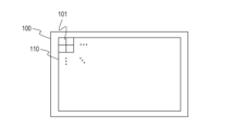
- FIG. 1A is a schematic diagram of a stacked photoelectric conversion device according to the first embodiment.
- the first substrate 100 and the second substrate 200 are semiconductor substrates, and as shown in FIG. 1B, the first substrate 100 has a pixel array portion 110 in which a plurality of unit pixels 101 are arranged over a plurality of rows and columns. are doing.
- the plurality of unit pixels 101 may be arranged in one row and multiple columns, or may be arranged in multiple columns and rows.
- the unit pixels 101 typically consist of tens of millions of pixels.
- the photoelectric conversion device of this embodiment is a backside illumination type photoelectric conversion device in which light is incident from the first substrate 100 side. Furthermore, a signal line (not shown) is provided between the photoelectric conversion section and the joint surface 300 .
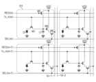
- FIG. 15 is a circuit diagram showing a circuit of the unit pixel 101 of 2 rows and 1 column among the unit pixels 101 shown in FIGS. 1A and 1B.
- charges accumulated in a photodiode which is a photoelectric conversion unit, are electrons.
- all the transistors included in the unit pixel 101 are N-type transistors.
- the charges accumulated by the photodiode may be holes, and in this case, the transistor of the unit pixel 101 may be a P-type transistor.
- the definition of the conductivity type used in the following description can be changed according to the polarity of the charge treated as a signal.
- the unit pixel 101 has photodiodes D1 and D2, which are photoelectric conversion units, transfer transistors M1 and M2, a charge conversion unit C1, a reset transistor M3, an amplification transistor M4, and a selection transistor M5.
- the transfer transistor M1 is provided in an electrical path between the photodiode D1 and a node to which the charge converter C1, the reset transistor M3, and the amplification transistor M4 are connected.
- the transfer transistor M2 is provided in an electrical path between the node to which the charge converter C1, the reset transistor M3, and the amplification transistor M4 are connected, and the photodiode D2.
- the charge conversion section C1 is also called a floating diffusion section (FD section).
- a power supply voltage VDD is applied to the reset transistor M3 and the amplification transistor M4.
- the selection transistor M5 is provided in an electrical path between the amplification transistor M4 and the column signal line 10.
- FIG. It can be said that the amplification transistor M4 is electrically connected to the vertical output line 10 via the selection transistor M5.
- the charge conversion unit C1 includes a floating diffusion capacitance provided in the semiconductor substrate and a parasitic capacitance of an electrical path from the transfer transistor M1 to the amplification transistor M5 via the floating diffusion capacitance.
- Each of the signal RES, the signal Tx_A, and the signal SEL is a signal supplied via the control line 30 from the vertical scanning circuit (not shown) shown in FIGS. 1A and 1B.
- the pixel row to which the signal is supplied is added to the end of each signal.
- the signal RES(m) means the signal RES supplied to the m-th row pixels.
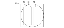
- Photodiodes D1 and D2 are arranged corresponding to one microlens ML, as shown in FIG. 16A. That is, the photodiodes D1 and D2 are arranged to receive the light transmitted through one microlens ML. Accordingly, phase difference detection type focus detection can be performed.
- All of the plurality of pixels that receive incident light provided in the pixel array may have the configuration of FIG. 16A.
- only some of the pixels may have the configuration shown in FIG. 16A, and another portion of the pixels may have one photodiode D1 shown in FIG.
- a current source (not shown) is connected to each of the vertical output lines 10-1 and 10-2.
- the selection transistor M5 of the unit pixel 101 in the m-th row is turned on.
- current is supplied from the current source to the amplification transistor M4 of the unit pixel 101 in the m-th row.
- a source follower circuit is formed by the power supply voltage VDD, the amplification transistor M4, and a current source (not shown) connected to the vertical output line 10-1.
- the amplification transistor M4 outputs a signal based on the potential of the charge converter C1 to the vertical output line 10-1 via the transistor M5.
- the selection transistor M5 of the unit pixel 101 in the m+1 row is turned on.
- current is supplied from the current source to the amplification transistor M4 in the (m+1)th row.
- a source follower circuit is formed by the power supply voltage VDD, the amplification transistor M4, and a current source (not shown) connected to the vertical output line 10-2.
- the amplification transistor M4 outputs a signal based on the potential of the charge converter C1 to the vertical output line 10-2 via the transistor M5.
- the unit pixels 101 in the m-th row and the unit pixels 101 in the m+1-th row are connected to different vertical output lines 10, respectively.
- one vertical output line 10 may be provided for one column of unit pixels 101, or the number of vertical output lines 10 may be greater than two. Also good.
- the photoelectric conversion portion may be an avalanche photodiode, and any device that performs photoelectric conversion may be used.
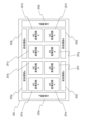
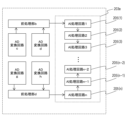
- the second substrate 200 has a plurality of AD conversion circuits 201a to 201h for converting analog signals output from the unit pixels 101 into digital signals.
- the second substrate 200 also has a plurality of preprocessing units 202a to 202d for converting the digital data output from the AD conversion circuits 201a to 201h into image data.
- the second substrate 200 further includes a plurality of AI processing units 203a and 203b, which are signal processing units for executing processing based on a neural network calculation model on the image data converted by the preprocessing units 202a to 202d. have.
- the AI processing units 203a and 203b are also provided with memory units that store learning models obtained by learning weighting coefficients of neural networks.
- the first substrate 100 and the second substrate 200 shown in FIGS. 1A, 1B, and 3 are bonded together at a bonding surface 300 to form a stacked photoelectric conversion device.
- FIGS. 1A, 1B, and 3 show the unit pixel 101, AD conversion circuits 201a to 201h, preprocessing units 202a to 202d, and AI processing units 203a and 203b as elements constituting the photoelectric conversion device.
- control lines for controlling the unit pixels 101 as shown in FIG. 2 and vertical output lines for transmitting signals output by the unit pixels 101 are arranged on the first substrate 100 as appropriate.
- a vertical scanning circuit, a driving circuit such as a timing generator, and an output circuit for outputting image data are arranged on the first substrate 100 or the second substrate 200 as appropriate.
- the analog signal output from the unit pixel 101 of the first substrate 100 is converted to one of the adjacent AD conversion circuits 201a to 201h of the second substrate 200 according to the position where the unit pixel 101 is arranged on the first substrate 100. Input to the conversion circuit. For example, an analog signal output from the upper left pixel 101 as viewed from the top surface of FIG. Similarly, an analog signal output from the lower right pixel 101 is input to an AD conversion circuit 201 h arranged on the lower right of the second substrate 200 .
- a plurality of AD converters arranged over a plurality of rows and a plurality of columns are arranged in each of the AD conversion circuits 201a to 201h.
- Each of the plurality of AD converters is arranged corresponding to one of the vertical output lines 10-n shown in FIG.
- the AD conversion format of this AD converter is not particularly limited, and various AD conversion formats such as slope type, ⁇ type, and successive approximation type can be applied.
- the digital data which are digital signals output from the AD conversion circuits 201a to 201h, are processed by the preprocessing section 202a of the second substrate 200 according to the positions at which the AD conversion circuits 201a to 201h are arranged on the second substrate 200.
- ⁇ d is input to the adjacent signal processing circuit.
- the digital data output from the AD conversion circuits 201a and 202b are input to the signal processing circuit 202a, and similarly the digital data output from the AD conversion circuits 201g and 202h are input to the preprocessing section 202d.
- the preprocessing units 202a to 202h perform signal processing on the digital signal output from the corresponding AD conversion circuit 201.
- signal processing in addition to CDS (Correlated Double Sampling), processing equivalent to part of image processing such as offset removal and amplification processing may be performed.
- the preprocessing unit 202 converts the format of the image data into YUV image data, RGB image data, or the like.
- the preprocessing unit 202 performs processing such as noise removal and white balance adjustment on the image data to be processed, if necessary.
- the preprocessing unit 202 performs various signal processing (also referred to as preprocessing) necessary for the AI processing unit 203 to process the image data to be processed.
- the AI processing units 203a and 203b execute processing based on the neural network calculation model on the image data converted by the adjacent preprocessing units 202a to 202d. For example, the image data converted by the preprocessing units 202a and 202c are processed by the AI processing unit 203a, and the image data converted by the preprocessing units 202b and 202d are processed by the AI processing unit 202b. process.
- the AD conversion unit includes AD conversion circuits a to h.
- This AD conversion section has two AD conversion circuits as a plurality of sets.
- One set includes AD conversion circuits 201a and 201b, and another set includes AD conversion circuits 201c and 201d.
- One preprocessing unit 202 is provided for two AD conversion circuits included in one set. That is, one set includes two AD conversion circuits and one preprocessing section.
- Each of the AI processing units 203a and 203b is arranged corresponding to two sets.
- the AI processing unit 203a which is the first signal processing unit, is arranged so as to correspond to the AD conversion circuits 201a and 201b included in one of the plurality of sets.
- the AI processing unit 203b which is the second signal processing unit, is arranged so as to correspond to the AD conversion circuits 201c and 201d included in another set of the plurality of sets.
- the plurality of sets are arranged in a plurality of rows and a plurality of columns. The plurality of sets are arranged between the first signal processing section and the second signal processing section.
- the AI processing units 203a and 203b are arranged on the left and right sides of the second substrate 200 as shown in FIG. Processing based on a neural network calculation model generally consumes a large amount of power, and the amount of heat generated by the AI processing unit is also large.
- the heat generated in the second substrate 200 also propagates to the first substrate 100 side through the bonding surface 300, and the dark current increases in the pixel array 100 due to the unit pixel 101 that receives the heat, and the dark current increases due to temperature unevenness. non-uniformity (unevenness) occurs.
- the uneven dark current generated in the pixel array 100 causes image data output from the stacked photoelectric conversion device to be uneven, which not only degrades image quality, but also makes image quality correction processing difficult.
- a plurality of AI processing units 203 By arranging a plurality of AI processing units 203 as shown in FIG. 3, local heat generation in the second substrate 200 can be reduced. As a result, the non-uniformity of the dark current can be reduced, and the output unevenness of the image data can be reduced.
- a plurality of AD conversion circuits are treated as one set, and the AI processing unit 203 is provided so as to correspond to each of the plurality of sets, thereby enabling parallel processing and realizing high-speed machine learning processing. can.
- the heat generated in the AI processing unit 203 can be more preferably dispersed. can.
- the influence of the heat generated by the second substrate 200 on the pixel array 100 of the first substrate 100 can be more preferably reduced.
- the AI processing units 203a and 203b are arranged on the left and right sides of the second substrate 200 in the present embodiment, they may be arranged on the upper and lower sides.
- the configuration in which the first substrate 100 and the second substrate 200 are laminated has been described as an example in the present embodiment, the configuration is not limited to this, and a configuration in which another semiconductor substrate is provided may be used.
- a third substrate may be arranged between the first substrate 100 and the second substrate 200 .
- a memory element may be arranged on the third substrate.
- the AI processing portions be arranged on the opposing two sides, three sides, or four sides on the second substrate.
- the AI processing unit in a region other than directly below the pixel array unit 110 arranged on the first substrate 100, the influence of the heat generated by the AI processing unit on the unit pixel 101 can be minimized. It becomes possible.
- a light-shielding pixel is a pixel arranged to detect an optical black level (black level), and a light-shielding pixel is light-shielded by a light-shielding film such as metal. If the amount of heat generated by the light-shielded pixels is small, the optical black level can be obtained normally, and the output values of the unit pixels other than the light-shielded pixels whose values have changed due to heat generation can be corrected.
- the light-shielding pixels may be provided so as to surround the four sides of the pixel array section, but they may be arranged on two sides like an L-shape.
- the AI processing units are arranged only in the vicinity of the two sides where the light-shielding pixels are not arranged, and the AI processing units are arranged on the two sides where the light-shielding pixels are arranged. You can choose not to distribute it. In this case, it is possible to make the light-shielded pixels less susceptible to the heat generated by the AI processing unit.
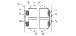
- FIGS. 16B and 16C show a configuration in which four photodiodes D1 to D4 are provided as four photoelectric conversion units for one microlens ML.
- a transfer transistor is provided corresponding to each of the photodiodes D1 to D4, and the gates G1 to G4 are gate electrodes of the corresponding transfer transistors.
- FIG. 16B gates G1, G3 transfer charge to pixel readout circuit R1.
- Gates G2 and G4 transfer charge to pixel readout circuit R2.
- Each of the pixel readout circuits R1 and R2 is provided with the capacitive element C1 shown in FIG.
- FIG. 16C is a form in which gates G1 to G4 are provided to transfer charges to one capacitive element C1. Even in such a form, the present embodiment can be suitably implemented.
- phase difference detection type focus detection can be performed by reading signals (focus detection signals) from some of the unit pixels 101 and some of the other unit pixels 101 . It is sufficient that at least some of the plurality of pixels provided in the pixel array have a configuration in which focus detection signals can be read out.
- the present embodiment has a configuration of the unit pixel 101 capable of phase difference detection.
- the AI processing section can further perform the focus detection operation.
- a detection unit 244 that performs focus detection may be provided on the second substrate 200 in addition to the AI processing unit.
- the arrangement of the second substrate of the detection section 244 is not particularly limited, but in the form of FIG. With respect to the AI processing unit and the detection unit 244 that generate heat, the temperature of the second substrate 200 can be easily made uniform by providing the detection unit 244 at a position away from the AI processing unit.
- FIG. 18 shows an example of the joining form of the first substrate 100 and the second substrate 200 of this embodiment.
- a first layer CFL is provided between the microlens ML and the first substrate 100 .
- An antireflection film, a color filter, and the like are provided on the first layer CFL.
- the first structure layer CFL may include a fixed charge film disposed on the first surface (incident surface) of the first substrate 100 .
- Photodiodes D1 and D2 are provided on the first substrate 100 .
- Gates G1 and G2 of transfer transistors are arranged on the second surface of the first substrate 100 .
- Gates of other transistors are also disposed on the second side of the first substrate 100 (not shown).
- the second structural layer L1 has a plurality of wiring layers and a plurality of interlayer insulating films. Wiring layers M1 and M2 are shown as a plurality of wiring layers.
- the second structural layer L1 has a first conductive portion MB11. The first conductive portion MB11 is connected to the wiring layer M2 by a plurality of interlayer connection portions TH1 and TH2.
- the third structural layer L2 also includes multiple wiring layers and multiple interlayer insulating films.
- a wiring layer M21 is shown as one of the plurality of wiring layers.
- the third structural layer L2 has a second conductive portion MB21. The contact between the first conductive portion MB11 and the second conductive portion MB21 results in electrical continuity.
- a bonding portion BD1 is formed by the first conductive portion MB11 and the second conductive portion MB21.
- An insulating film is formed on the surface on which the conductive portion MB11 is provided.
- An insulating film is formed on the surface on which the conductive portion MB21 is provided.
- the insulating film provided on the surface provided with the conductive portion MB11 and the insulating film provided on the surface provided with the conductive portion MB21 are bonded to each other. That is, at the bonding surface between the second structural layer L1 and the third structural layer L2, the bonding between the conductive portion MB11 and the conductive portion MB21, the insulating film included in the second structural layer L1, and the insulating film included in the third structural layer L2 are The junction is made by The insulating film included in the second structural layer L1 and the insulating film included in the third structural layer L2 are films containing silicon and oxygen.
- the second conductive portion MB21 is connected to the wiring layer M21 by a plurality of interlayer connection portions TH3 and TH4.
- the interlayer connection portions TH1, TH2, TH3, and TH4 may be made of a conductive material such as tungsten.
- the wiring layers M1, M2, and M21 may also be made of a conductive material, such as copper or aluminum.
- the first conductive portion MB11 and the second conductive portion MB21 forming the bonding portion BD1 may also be made of a conductive material, such as copper.
- a well region WEL is provided on the second substrate 200 .
- a gate SG of each transistor is arranged between the second substrate 200 and the wiring layer.
- FIG. 17 shows several junction structures ST1 to ST4.
- the structure ST1 including the bonding portion BD1 described above is a structure in which one electrical node is formed by one first conductive portion and one second conductive portion.
- Structures ST2-ST4 are structures in which one electrical node is formed by a plurality of junctions.
- one wiring included in the second structural layer L1 is connected to multiple junctions BD2 and BD3.
- one wiring included in the third structural layer L2 is connected to the joint BD2, and another wiring is connected to the joint BD3.
- one wiring included in the second structural layer L1 is connected to the junction BD4, and another wiring is connected to the junction BD5.
- one wiring included in the third structural layer L2 is connected to the junctions BD4 and BD5.
- one wiring included in the second structural layer L1 is connected to the junctions BD6 and BD7.
- one wiring included in the third structural layer L2 is connected to the junctions BD6 and BD7.
- These structures ST1 to ST4 can be used properly according to the location of the photoelectric conversion device and the signal (voltage) to be transmitted.
- one of the structures ST2 to ST4 is selected in order to reduce the resistance value of the transmission path.
- the path for transmitting a signal for each row or each column of the unit pixel 101 is restricted by the row pitch or the column pitch, so the structure ST1 is selected.
- the joints BD1 to BD7 and the connected wiring also act as heat radiation paths. Therefore, for a joint portion that overlaps an AI processed portion that generates a large amount of heat in a plan view, one of the structures ST2 to ST4 can be used to facilitate the release of heat generated in the AI processed portion.
- the structures ST3 and ST4 have one wiring between the second substrate 200 and a length connected to a plurality of joints. By providing a long wiring in the vicinity of the AI processing section that generates a large amount of heat, the heat can be released favorably.
- a plurality of interlayer connection portions TH1 to TH4 are connected to each of the first conductive portion MB11 and the second conductive portion MB21. This has the effect of facilitating heat release compared to the case where one interlayer connection is provided for each of the first conductive portion MB11 and the second conductive portion MB21.
- one of the structures ST2 to ST4 is used for a joint portion that overlaps an AI processing portion that generates a large amount of heat in a plan view.
- the other joint maintains electrical continuity. be able to.
- a plurality of photodiodes D1 and D2 are provided for one microlens, but one photodiode shown in FIG. 2 may be provided. Also, a phase difference detection type focus detection signal may be generated by shielding part of this one photodiode.
- the items described in this embodiment, including the configuration of FIG. 18, can be implemented in combination with the following embodiments. For example, the configurations shown in FIGS. 15 and 16A-16C can be applied to all of the following embodiments.
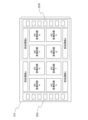
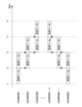
- FIG. 4 shows a configuration example of the second substrate 210 of the photoelectric conversion device according to this embodiment. Note that the AI processing units 203c and 203d are the same as those of the first embodiment, so description thereof is omitted.
- the AI processing units 203c and 203d have the same configuration and are arranged symmetrically at the left and right ends of the second substrate 210. As shown in FIG.
- FIG. 5 is an enlarged view of the dashed line part in FIG. n
- AI processing circuits 204 having the same function are arranged inside the AI processing unit 203d, and each AI processing circuit is electrically directly connected to the preprocessing units 202b and 202d.
- the preprocessing unit 202b and AI processing circuits 1, 2, 3, and 4 are connected, and the preprocessing unit 202d, AI processing circuit 5, and AI processing circuit n are directly connected.
- the number of AI processing circuits included in the AI processing units is greater than the number of preprocessing circuits 202 provided on the second substrate 200 . Thereby, the heat generated by the machine learning process can be more preferably reduced.
- the heat generated in the second substrate 210 can be dispersed by further dispersing the signal processing units that perform processing based on the neural network calculation model. This can reduce the influence of the heat generated on the second substrate 200 side on the pixel array 100 of the first substrate 100 .
- processing speed can be increased by performing processing based on the neural network calculation model in parallel using multiple AI processing circuits.
- FIG. 6 is an enlarged view of the dashed line portion of FIG. 4 in the second embodiment.
- the AI processing unit 203e shown in FIG. 6 is provided as the AI processing unit 203d shown in FIG.
- the same configuration as the AI processing unit 203e shown in FIG. 6 is also provided in the AI processing unit 203c shown in FIG. Note that the configuration other than the AI processing unit 203e is the same as in the first and second embodiments, so the description is omitted.
- AI processing circuits having a fixed circuit configuration capable of executing stepwise data processing are arranged, and each of the AI processing circuits 205(1) to 205(n) are electrically connected in series.
- the image data converted by the preprocessing unit is passed to the AI processing circuit 205(1), the AI processing circuit 205(2), and the AI processing circuit 205(3) in this order.
- a process based on is executed.
- the AI processing circuit 205(1) is electrically directly connected to the preprocessing section 202b, and the AI processing circuit 205(n) is electrically connected to the preprocessing section 202d.
- FIG. 7 is a timing chart schematically showing calculation operations based on the neural network calculation model performed by the AI processing circuit in this embodiment. From time t1 to t2, the AI processing circuit 205(1) performs processing based on the neural network calculation model on the image data (hereinafter referred to as image data c) converted by the preprocessing unit 202b. This image data c is based on the digital data output from the AD conversion circuit 201c.
- image data c is based on the digital data output from the AD conversion circuit 201c.
- the AI processing circuit 205(1) performs processing based on the neural network calculation model on the image data (hereinafter referred to as image data d) converted by the preprocessing unit 202b. Execute. This image data d is based on the digital data output from the AD conversion circuit 201d.
- the image data c is processed by the AI processing circuit 205(1) from time t1 to t2. Also, the image data c is processed by another AI processing circuit 205(2) from time t2 to t3.
- AI processing circuits 205(1) and (2) have different neural network calculation models. Therefore, AI processing circuit 205(2) performs processing based on a neural network calculation model different from the processing performed by AI processing circuit 205(1).
- the AI processing circuit 205(2) performs processing on the image data d based on a neural network calculation model different from the processing performed by the AI processing circuit 205(1). Also, the AI processing circuit 205(3) performs processing on the image data c based on a neural network calculation model different from the processing performed by the AI processing circuit 205(2).
- the AI processing circuit 205(3) performs processing on the image data d based on a neural network calculation model different from the processing performed by the AI processing circuit 205(2).
- the image data converted by the preprocessing unit 202d based on the digital data output from the AD conversion circuit 201g is denoted as image data d.
- image data converted by the signal processing circuit 202d based on the digital data output from the AD conversion circuit 201h is referred to as image data h.
- the AI processing circuit 205(n-2), the AI processing circuit 205(n-1), and the AI processing circuit 205(n) are processed from time t4 to t5, respectively. Processing based on different neural network computational models is performed sequentially. This processing is as shown in FIG.
- the AI processing unit of the photoelectric conversion device in this embodiment has a multi-stage pipeline configuration consisting of three stages, and executes processing based on a neural network calculation model in a sequential processing method.
- the layout of the AI processing circuits described in this embodiment is only an example, and it is desirable that the connection method of each AI processing circuit be appropriately laid out according to the amount of heat generated by each AI processing circuit and the number of stages of processing.
- the AI processing circuits are arranged in series from the upper and lower ends of the second substrate toward the center of the second substrate in a plan view viewed from above the second substrate. It is not limited to this example, and may be arranged in series from the center of the second substrate 200 toward the upper end and the lower end.
- the AI processing circuit connected to the preprocessing unit 202b may be arranged on the upper end of the second substrate
- the AI processing circuit connected to the preprocessing unit 202d may be arranged in the center of the second substrate.
- the direction of delivery of the image data converted by the preprocessing unit is the direction from the upper end side to the lower end side when viewed from the upper surface of the second substrate.
- heat generated in the second substrate 210 can be dispersed by further dispersing the processing units that perform processing based on the neural network calculation model. Therefore, the influence of the heat generated on the second substrate side on the pixel array 100 of the first substrate 100 can be reduced.
- the processing speed can be increased by performing processing based on the neural network calculation model in parallel using multiple AI processing circuits.
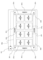
- FIG. 8 is a diagram showing the configuration of the second substrate 400 in this embodiment.
- the photoelectric conversion device according to the present embodiment has a configuration in which one AD converter 401 is provided on the second substrate 400 for one unit pixel 101 on the first substrate 100 . Thereby, analog signals output from all the unit pixels 101 can be collectively converted into digital data at the same time by the respective AD converters.
- 402a to 402d shown in FIG. 8 are preprocessing and AI processing units, respectively, which convert the digital data converted by the AD converter 401 into image data. Furthermore, processing based on a neural network calculation model is performed on the converted image data.
- the circuit regions for performing this preprocessing and AI processing are shown as 402a-d in FIG.
- the preprocessing unit and AI processing units 402a to 402d are a first signal processing unit, a second signal processing unit, a third signal processing unit, and a fourth signal processing unit, respectively.
- pads 800 for inputting signals (including power supply voltage) from the outside of the photoelectric conversion device or for outputting signals to the outside of the photoelectric conversion device are provided on four sides of the second substrate 200.
- a plurality of AI processing units are located in an area between the outer periphery provided with pads on four sides and the AD conversion unit (an area formed by the AD converters 401 provided over multiple rows and multiple columns). is provided.
- the pads 800 are provided on all four sides of the second substrate 200 in FIG. 8, they may be provided on two opposing sides.
- the digital data output from the AD converter 401 is input to either the preprocessing unit or the AI processing units 402a to 402d depending on the position where the AD converter 401 is arranged on the second substrate 400.
- the elements that execute processing based on the neural network calculation model are arranged, and they are arranged at approximately equal intervals.
- the heat generated in the second substrate 400 by the AI processing section can be dispersed. Therefore, the influence of the heat generated on the second substrate side on the pixel array of the first substrate 100 can be reduced.
- processing based on a neural network calculation model can be performed in parallel using a plurality of AI processing units, making it possible to increase the processing speed.
- the AI processing unit described in this embodiment may have a circuit configuration that executes stepwise data processing as described in the third embodiment. That is, each AI processing circuit may be electrically connected in series, have a multistage pipeline configuration, and execute processing based on a neural network calculation model in a sequential processing method.
- the AI processing circuits in the preprocessing units and AI processing units 402a to 402d have a circuit configuration capable of performing stepwise data processing. connected in series.
- the preprocessing unit and the AI processing units 402a, 402b, 402c, and 403d may be connected so as to circle the second substrate 400, or only some of the AI processing units 402a to 402d may be connected.
- the AI processing units 402a and 402b are connected, the AI processing units 402c and 402d are connected. Then, the AI processing units 402a and 402b, and the AI processing units 402c and 402d perform sequential processing. The sequential processing of the AI processing units 402a and 402b, and the AI processing units 402c and 402d may be performed in parallel at the same time.
- different AI processing units perform signal processing for each frame.
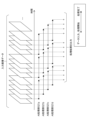
- FIG. 9 is a diagram showing the configuration of the second substrate 200 of this embodiment.
- the preprocessing unit 900a outputs the same data to both AI processing units 901a and 901b. Also, the preprocessing unit 900b outputs the same data to both the AI processing units 901a and 901b. That is, the AI processing units 901a and 901b receive the same data from the plurality of preprocessing units 900a and 900b. Various parameters of the AI processing units 901a and 901b are adjusted by machine learning, but the parameters are different between the AI processing units 901a and 901b. Therefore, even when the same data is input to the AI processing units 901a and 901b, the output results of the AI processing units 901a and 901b may differ.
- the output results of the AI processing units 901 a and 901 b are input to the integration processing unit 910 .
- the integration processing unit 910 performs one of the following operations when the output results of the AI processing units 901a and 901b are different. (1) Among the output results of the AI processing units 901a and 901b, a highly reliable output result is selected and output to the outside of the photoelectric conversion device. Select and output the corresponding result from the lookup table for the combination of the output results of 901a and 901b. output more information
- the determination of the reliability in (1) may be performed by referring to the output result of the AI processing unit 901 in the past. You can give Alternatively, each of the AI processing units 901a and 901b may output reliability information for the output result, and the one with the higher reliability information may be selected.
- the reliability information of (3) can cause each of the AI processing units 901a and 901b to output reliability information for the output result, and output the reliability information to the outside of the photoelectric conversion device.
- a plurality of AI processing units 901 perform signal processing involving machine learning processing on the same data. Thereby, the accuracy of the processing result output by the AI processing unit can be improved.
- the photoelectric conversion device of this embodiment can have redundancy in the AI processing unit.
- one of the AI processing units 901a and 901b may fail or the signal accuracy may be significantly degraded.
- the operation of the one AI processing unit can be stopped, or the output result can be ignored, and the output result of the other AI processing unit can be adopted.
- the operation of the photoelectric conversion device can be continued even if some of the AI processing units fail or the signal accuracy is degraded.
- the configuration of the photoelectric conversion device of this embodiment can be the same as that of the fifth embodiment, but can be configured with more AI processing units as shown in FIG. The following description is based on the configuration of FIG.
- each of the AD conversion circuits a to h can selectively output digital data to either one of the preprocessing units 900a and 900b, as shown for the AD conversion circuit a.
- each of the AD conversion circuits a to h may further include a configuration capable of outputting digital data in parallel with both the preprocessing units 900a and 900b.
- FIG. 11 is a diagram showing the operation of the AI processing unit of this embodiment.
- image data image data corresponding to one screen output of the AD conversion units 921a to 921h of each frame is shown.
- the AI processing unit 921a starts processing image data for n frames (n is a natural number). After that, while the AI processing unit 921a is processing the image data, another AI processing unit 921b starts processing the n+1 frame of image data. Similarly, while the AI processing units 921a and 921b are processing image data, the AI processing unit 921c starts processing n+3 frame image data. Similarly, while the AI processing units 921a, 921b, and 921c are processing image data, the AI processing unit 921d starts processing n+4 frame image data.
- the AI processing unit 921a finishes processing the image data and starts processing the n+5 frame image data again. Similar operations are repeated thereafter.
- the preprocessing unit 900a can selectively output digital data to the AI processing units 921a and 921b, so that the multiple frames of image data can be distributed frame by frame to the multiple AI processing units.
- AD conversion circuits a to h further include a configuration capable of selectively outputting digital data to either one of preprocessing units 900a and 900b. It facilitates the allocation of the AI processing part of
- the AD conversion circuits a to h are configured to selectively output digital data to either one of the preprocessing units 900a and 900b.
- the preprocessing units 900a and 900b may be made into one preprocessing unit 900, and this one preprocessing unit 900 may be distributed to the four AI processing units 921a to 921d.
- the number of AI processing units 921 is not limited to four, and may be two or more.
- the learned models held by the AI processing units 921a to 921d can be the same. As a result, even if different AI processing units 921 perform processing for each frame, it is possible to obtain an output result with the same level of reliability accuracy.
- each of the plurality of AI processing units 921a to 921d independently performs machine learning. This machine learning may or may not use teacher data.
- the AI processing units 921a to 921d After the AI processing units 921a to 921d complete machine learning, they input a signal whose expected output result is known to the photoelectric conversion device. For example, assuming that "the subject is a human face" as an expected output result, an example in which a photoelectric conversion device is caused to image a human face will be described.
- the integration processing unit 910 receives the output results of the AI processing units 921a to 921d.
- the integrated processing unit 910 increases the reliability of the AI processing unit 921 that outputs the correct output result (“the subject is a human face”) among the AI processing units 921a to 921d.
- the photoelectric conversion device repeats the operation of comparing the expected output result and the actual output result of the AI processing unit 921 .
- the integrated processing unit 910 identifies the AI processing unit 921 that is likely to output correct output results among the AI processing units 921a to 921d.
- the integrated processing unit 910 applies the learned model of the identified AI processing unit 921 to the other AI processing units 921 .
- the AI processing units 921a to 921d can have a common trained model with high reliability.
- the configuration of the photoelectric conversion device of this embodiment can be the same as that of the sixth embodiment.
- the integrated processing unit 910 outputs the processing results to the outside of the photoelectric conversion device based on the output results of the multiple frames output by the multiple AI processing units.
- FIG. 12 is a diagram showing operations of the AI processing units 921a to 921d shown in FIG. 10 in this embodiment. The difference from the operation shown in FIG. 11 is that the integrated processing unit 910 performs comprehensive judgment from the output results of the plurality of AI processing units 921a to 921d and outputs the processing result to the outside of the photoelectric conversion device.
- the most output result among the output results of the plurality of AI processing units 921a to 921d is adopted and output.
- the plurality of AI processing units 921a to 921d may have the same learned model as described in the sixth embodiment.
- the plurality of AI processing units 921a to 921d may have different trained models.
- a signal whose expected output result is known is input to the photoelectric conversion device.
- the integration processing unit 910 receives the output results of the AI processing units 921a to 921d. It is assumed that some AI processing units output an output result that "the subject is a human face” and other AI processing units output an output result other than "the subject is a human face”.
- the integrated processing unit 910 increases the reliability of the AI processing unit 921 that outputs the correct output result (“the subject is a human face”) among the AI processing units 921a to 921d.
- the photoelectric conversion device repeats the operation of comparing the expected output result and the actual output result of the AI processing unit 921 .
- the integrated processing unit 910 determines the reliability of each of the AI processing units 921a to 921d.
- the integration processing unit 910 assigns reliability parameters to the output results of the plurality of AI processing units 921a to 921d, and determines the processing results to be output to the outside of the photoelectric conversion device.
- each of the plurality of AI processing units 921a to 921d processes image data of different frames.
- image data of the same frame may be processed by a plurality of AI processing units 921a to 921d.
- the integrated processing unit 910 may perform comprehensive determination as described in the present embodiment, and output the processing result to the outside of the photoelectric conversion device.
- FIG. 14 shows the projection positions of the pixel array section 110 provided on the first substrate on the second substrate when viewed from above.
- the AI processing units 203a and 203b are provided at positions that do not overlap with the pixel array unit 110 in plan view.
- the pixel array section 110 is less susceptible to heat generation from the AI processing section.
- the preprocessing units 202a to 202d are also provided at positions that do not overlap with the pixel array unit 110 in plan view. As a result, the pixel array section 110 is less likely to be affected by heat generated in the preprocessing sections 202a to 202d.
- the operation processing speed may be made different for a plurality of AI processing units.
- the AI processing unit with the faster operation processing speed may be set further away from the pixel array position in plan view than the AI processing unit with the lower operation processing speed.
- the AI processing unit having a high operation processing speed also generates a large amount of heat, it is possible to reduce the influence of the heat generated by the AI processing unit on the pixel array unit.
- the AI processing section may be provided on the first substrate.
- FIG. 19 is a block diagram showing the configuration of a photoelectric conversion system 11200 according to this embodiment.
- a photoelectric conversion system 11200 of this embodiment includes a photoelectric conversion device 11204 .
- any of the photoelectric conversion devices described in the above embodiments can be applied to the photoelectric conversion device 11204 .
- the photoelectric conversion system 11200 can be used, for example, as an imaging system. Specific examples of imaging systems include digital still cameras, digital camcorders, surveillance cameras, network cameras, and the like.
- FIG. 19 shows an example of a digital still camera as the photoelectric conversion system 11200 .
- a photoelectric conversion system 11200 shown in FIG. 19 has a photoelectric conversion device 11204 and a lens 11202 that forms an optical image of a subject on the photoelectric conversion device 11204 .
- the photoelectric conversion system 11200 also has an aperture 11203 for varying the amount of light passing through the lens 11202 and a barrier 11201 for protecting the lens 11202 .
- a lens 11202 and a diaphragm 11203 are an optical system for condensing light onto the photoelectric conversion device 11204 .
- the photoelectric conversion system 11200 has a signal processing unit 11205 that processes the output signal output from the photoelectric conversion device 11204 .
- the signal processing unit 11205 performs a signal processing operation of performing various corrections and compressions on an input signal and outputting the signal as necessary.
- the photoelectric conversion system 11200 further has a buffer memory section 11206 for temporarily storing image data, and an external interface section (external I/F section) 11209 for communicating with an external computer or the like.
- the photoelectric conversion system 11200 includes a recording medium 11211 such as a semiconductor memory for recording or reading image data, and a recording medium control interface section (recording medium control I/F section) for recording or reading the recording medium 11211. 11210.
- the recording medium 11211 may be built in the photoelectric conversion system 11200 or may be detachable. Communication from the recording medium control I/F unit 11210 to the recording medium 11211 and communication from the external I/F unit 11209 may be performed wirelessly.
- the photoelectric conversion system 11200 has an overall control/calculation unit 11208 that performs various calculations and controls the entire digital still camera, and a timing generation unit 11207 that outputs various timing signals to the photoelectric conversion device 11204 and the signal processing unit 11205 .
- a timing signal or the like may be input from the outside, and the photoelectric conversion system 11200 may include at least a photoelectric conversion device 11204 and a signal processing unit 11205 that processes an output signal output from the photoelectric conversion device 11204. good.
- the overall control/arithmetic unit 11208 and the timing generation unit 11207 may be configured to implement some or all of the control functions of the photoelectric conversion device 11204 .
- the photoelectric conversion device 11204 outputs the image signal to the signal processing unit 11205 .
- a signal processing unit 11205 performs predetermined signal processing on the image signal output from the photoelectric conversion device 11204 and outputs image data. Also, the signal processing unit 11205 generates an image using the image signal. Also, the signal processing unit 11205 may perform ranging calculation on the signal output from the photoelectric conversion device 11204 .
- the signal processing unit 11205 and the timing generation unit 11207 may be mounted on the photoelectric conversion device. That is, the signal processing unit 11205 and the timing generation unit 11207 may be provided on the substrate on which the pixels are arranged, or may be provided on another substrate.
- FIG. 20 is a block diagram showing a configuration example of a distance image sensor, which is electronic equipment using the photoelectric conversion device described in the above embodiments.
- the distance image sensor 12401 comprises an optical system 12407, a photoelectric conversion device 12408, an image processing circuit 12404, a monitor 12405, and a memory 12406.
- the distance image sensor 12401 receives the light (modulated light or pulsed light) projected from the light source device 12409 toward the subject and reflected by the surface of the subject, thereby producing a distance image corresponding to the distance to the subject. can be obtained.
- the optical system 12407 includes one or more lenses, guides image light (incident light) from a subject to the photoelectric conversion device 12408, and forms an image on the light receiving surface (sensor portion) of the photoelectric conversion device 12408.
- the photoelectric conversion device of each embodiment described above is applied as the photoelectric conversion device 12408 , and a distance signal indicating the distance obtained from the received light signal output from the photoelectric conversion device 12408 is supplied to the image processing circuit 12404 .
- the image processing circuit 12404 performs image processing to construct a distance image based on the distance signal supplied from the photoelectric conversion device 12408 .
- a distance image (image data) obtained by the image processing is supplied to the monitor 12405 to be displayed, or supplied to the memory 406 to be stored (recorded).
- the range image sensor 12401 configured in this way, by applying the above-described photoelectric conversion device, it is possible to obtain, for example, a more accurate range image as the characteristics of the pixels are improved.
- the technology (the present technology) according to the present disclosure can be applied to various products.
- the technology according to the present disclosure may be applied to an endoscopic surgery system.
- FIG. 21 is a diagram showing an example of a schematic configuration of an endoscopic surgery system to which the technology according to the present disclosure (this technology) can be applied.
- FIG. 21 shows how an operator (physician) 13131 is performing surgery on a patient 13132 on a patient bed 13133 using an endoscopic surgery system 13003 .
- the endoscopic surgery system 13003 is composed of an endoscope 13100, a surgical tool 13110, and a cart 13134 on which various devices for endoscopic surgery are mounted.
- An endoscope 13100 is composed of a lens barrel 13101 having a predetermined length from its distal end inserted into the body cavity of a patient 13132 and a camera head 13102 connected to the proximal end of the lens barrel 13101 .
- an endoscope 13100 configured as a so-called rigid scope having a rigid lens barrel 13101 is illustrated, but the endoscope 13100 may be configured as a so-called flexible scope having a flexible lens barrel. good.
- the tip of the lens barrel 13101 is provided with an opening into which the objective lens is fitted.
- a light source device 13203 is connected to the endoscope 13100 , and light generated by the light source device 13203 is guided to the tip of the lens barrel 13101 by a light guide extending inside the lens barrel 13101 . This light is directed through an objective lens toward an object of observation within the body cavity of the patient 13132 .
- the endoscope 13100 may be a straight scope, a perspective scope, or a side scope.
- An optical system and a photoelectric conversion device are provided inside the camera head 13102, and the reflected light (observation light) from the observation target is focused on the photoelectric conversion device by the optical system.
- the photoelectric conversion device photoelectrically converts the observation light to generate an electrical signal corresponding to the observation light, that is, an image signal corresponding to the observation image.
- the photoelectric conversion device the photoelectric conversion device described in each of the above embodiments can be used.
- the image signal is transmitted to a camera control unit (CCU: Camera Control Unit) 13135 as RAW data.
- CCU Camera Control Unit
- the CCU 13135 is composed of a CPU (Central Processing Unit), a GPU (Graphics Processing Unit), etc., and controls the operations of the endoscope 13100 and the display device 13136 in an integrated manner. Further, the CCU 13135 receives an image signal from the camera head 13102 and performs various image processing such as development processing (demosaicing) for displaying an image based on the image signal.
- image processing such as development processing (demosaicing) for displaying an image based on the image signal.
- the display device 13136 displays an image based on the image signal subjected to image processing by the CCU 13135 under the control of the CCU 13135 .
- the light source device 13203 is composed of, for example, a light source such as an LED (Light Emitting Diode), and supplies the endoscope 13100 with irradiation light for photographing a surgical site or the like.
- a light source such as an LED (Light Emitting Diode)
- LED Light Emitting Diode
- the input device 13137 is an input interface for the endoscopic surgery system 13003.
- the user can input various information and instructions to the endoscopic surgery system 13003 via the input device 13137 .
- the treatment instrument control device 13138 controls driving of the energy treatment instrument 13112 for tissue cauterization, incision, or blood vessel sealing.
- the light source device 13203 that supplies irradiation light to the endoscope 13100 for photographing the surgical site can be composed of, for example, a white light source composed of an LED, a laser light source, or a combination thereof.
- a white light source is configured by combining RGB laser light sources, the output intensity and output timing of each color (each wavelength) can be controlled with high accuracy. It can be carried out.
- the object to be observed is irradiated with laser light from each of the RGB laser light sources in a time division manner, and by controlling the drive of the imaging element of the camera head 13102 in synchronization with the irradiation timing, each of RGB can be handled. It is also possible to pick up images by time division. According to this method, a color image can be obtained without providing a color filter in the imaging element.
- the driving of the light source device 13203 may be controlled so as to change the intensity of the output light every predetermined time.
- the drive of the imaging device of the camera head 13102 in synchronism with the timing of the change in the intensity of the light to obtain images in a time-division manner and synthesizing the images, a high dynamic A range of images can be generated.
- the light source device 13203 may be configured to be capable of supplying light in a predetermined wavelength band corresponding to special light observation.
- Special light observation for example, utilizes the wavelength dependence of light absorption in body tissues. Specifically, a predetermined tissue such as a blood vessel on the surface of the mucous membrane is imaged with high contrast by irradiating light with a narrower band than the irradiation light (that is, white light) used during normal observation.
- irradiation light that is, white light
- fluorescence observation may be performed in which an image is obtained from fluorescence generated by irradiation with excitation light.
- body tissue is irradiated with excitation light and fluorescence from the body tissue is observed, or a reagent such as indocyanine green (ICG) is locally injected into the body tissue and the fluorescence wavelength of the reagent is observed in the body tissue. It is possible to obtain a fluorescent image by irradiating excitation light corresponding to .
- the light source device 13203 can be configured to supply narrowband light and/or excitation light corresponding to such special light observation.
- FIGS. 22A and 22B are schematic diagrams showing configuration examples of a photoelectric conversion system and a moving object according to this embodiment.
- an example of an in-vehicle camera is shown as a photoelectric conversion system.
- FIGs. 22A and 22B show an example of a vehicle system and a photoelectric conversion system mounted therein for imaging.
- a photoelectric conversion system 14301 includes a photoelectric conversion device 14302 , an image preprocessing unit 14315 , an integrated circuit 14303 and an optical system 14314 .
- the optical system 14314 forms an optical image of a subject on the photoelectric conversion device 14302 .
- the photoelectric conversion device 14302 converts the optical image of the object formed by the optical system 14314 into an electrical signal.
- the photoelectric conversion device 14302 is the photoelectric conversion device according to any one of the embodiments described above.
- An image preprocessing unit 14315 performs predetermined signal processing on the signal output from the photoelectric conversion device 14302 .
- the function of the image preprocessing unit 14315 may be incorporated within the photoelectric conversion device 14302 .
- the photoelectric conversion system 14301 is provided with at least two sets of an optical system 14314, a photoelectric conversion device 14302, and an image preprocessing unit 14315, and the output from each set of image preprocessing units 14315 is input to an integrated circuit 14303. It's like
- the integrated circuit 14303 is an integrated circuit for use in imaging systems, and includes an image processing unit 14304 including a memory 14305, an optical distance measurement unit 14306, a distance calculation unit 14307, an object recognition unit 14308, and an abnormality detection unit 14309.
- An image processing unit 14304 performs image processing such as development processing and defect correction on the output signal of the image preprocessing unit 14315 .
- the memory 14305 temporarily stores captured images and stores defect positions of captured pixels.
- An optical distance measuring unit 14306 performs focusing of a subject and distance measurement.
- a ranging calculation unit 14307 calculates ranging information from a plurality of image data acquired by a plurality of photoelectric conversion devices 14302 .
- the object recognition unit 14308 recognizes subjects such as cars, roads, signs, and people.
- the abnormality detection unit 14309 detects an abnormality in the photoelectric conversion device 14302, the abnormality detection unit 14309 notifies the main control unit 14313 of the abnormality.
- the integrated circuit 14303 may be realized by specially designed hardware, software modules, or a combination thereof. Also, it may be realized by FPGA (Field Programmable Gate Array), ASIC (Application Specific Integrated Circuit), etc., or by a combination thereof.
- FPGA Field Programmable Gate Array
- ASIC Application Specific Integrated Circuit
- the main control unit 14313 integrates and controls the operations of the photoelectric conversion system 14301, the vehicle sensor 14310, the control unit 14320, and the like. There is also a method in which the photoelectric conversion system 14301, the vehicle sensor 14310, and the control unit 14320 have individual communication interfaces without the main control unit 14313, and each of them transmits and receives control signals via a communication network (for example, CAN standard).
- a communication network for example, CAN standard
- the integrated circuit 14303 has a function of receiving a control signal from the main control unit 14313 or transmitting a control signal and setting values to the photoelectric conversion device 14302 by its own control unit.
- the photoelectric conversion system 14301 is connected to a vehicle sensor 14310, and can detect the running state of the own vehicle such as vehicle speed, yaw rate, and steering angle, the environment outside the own vehicle, and the state of other vehicles and obstacles.
- the vehicle sensor 14310 also serves as distance information acquisition means for acquiring distance information to an object.
- the photoelectric conversion system 14301 is also connected to a driving support control unit 1311 that performs various driving support functions such as automatic steering, automatic cruise, and anti-collision functions.
- the collision determination function based on the detection results of the photoelectric conversion system 14301 and the vehicle sensor 14310, it is possible to estimate a collision with another vehicle/obstacle and determine whether or not there is a collision. As a result, avoidance control when a collision is presumed and safety device activation at the time of collision are performed.
- the photoelectric conversion system 14301 is also connected to an alarm device 14312 that issues an alarm to the driver based on the judgment result of the collision judgment section. For example, when the collision possibility is high as a result of the judgment by the collision judging section, the main control section 14313 controls the vehicle to avoid collision and reduce damage by applying the brake, releasing the accelerator, or suppressing the engine output. conduct.
- the alarm device 14312 warns the user by sounding an alarm such as sound, displaying alarm information on a display unit screen of a car navigation system or a meter panel, or vibrating a seat belt or steering wheel.
- the photoelectric conversion system 14301 photographs the surroundings of the vehicle, for example, the front or rear.
- FIG. 22B shows an arrangement example of the photoelectric conversion system 14301 when the photoelectric conversion system 14301 captures an image in front of the vehicle.
- the two photoelectric conversion devices 14302 are arranged in front of the vehicle 14300 .
- the center line of the vehicle 14300 with respect to the forward/retreat azimuth or outer shape (for example, vehicle width) is regarded as a symmetrical axis
- the two photoelectric conversion devices 1302 are arranged line-symmetrically with respect to the symmetrical axis.
- This form is preferable for obtaining information on the distance between the vehicle 14300 and the object to be photographed and for determining the possibility of collision.
- the photoelectric conversion device 14302 is preferably arranged so as not to block the driver's field of view when the driver visually recognizes the situation outside the vehicle 14300 from the driver's seat. It is preferable that the warning device 14312 be arranged so as to be easily visible to the driver.
- the control that does not collide with another vehicle has been described, but it is also applicable to control that automatically drives following another vehicle, control that automatically drives so as not to stray from the lane, and the like.
- the photoelectric conversion system 14301 can be applied not only to a vehicle such as a vehicle, but also to a moving object (moving device) such as a ship, an aircraft, or an industrial robot.
- the present invention can be applied not only to mobile objects but also to devices that widely use object recognition, such as intelligent transportation systems (ITS).
- ITS intelligent transportation systems
- the photoelectric conversion device of the present invention may further have a configuration capable of acquiring various information such as distance information.
- FIG. 23A and 23B illustrate eyeglasses 16600 (smart glasses) according to one application.
- Glasses 16600 have a photoelectric conversion device 16602 .
- the photoelectric conversion device 16602 is the photoelectric conversion device described in each of the above embodiments.
- a display device including a light-emitting device such as an OLED or an LED may be provided on the rear surface side of the lens 16601 .
- One or more photoelectric conversion devices 16602 may be provided. Further, a plurality of types of photoelectric conversion devices may be used in combination.
- the arrangement position of the photoelectric conversion device 16602 is not limited to that shown in FIG. 23A.
- the spectacles 16600 further include a control device 16603.
- the control device 16603 functions as a power source that supplies power to the photoelectric conversion device 16602 and the display device.
- the control device 16603 controls operations of the photoelectric conversion device 16602 and the display device.
- the lens 16601 is formed with an optical system for condensing light onto the photoelectric conversion device 16602 .
- FIG. 23B illustrates glasses 16610 (smart glasses) according to one application.
- the glasses 16610 have a control device 16612, and the control device 16612 is equipped with a photoelectric conversion device corresponding to the photoelectric conversion device 16602 and a display device.
- a photoelectric conversion device in the control device 16612 and an optical system for projecting light emitted from the display device are formed on the lens 16611 , and an image is projected onto the lens 16611 .
- the control device 16612 functions as a power source that supplies power to the photoelectric conversion device and the display device, and controls the operation of the photoelectric conversion device and the display device.
- the control device may have a line-of-sight detection unit that detects the line of sight of the wearer.
- Infrared rays may be used for line-of-sight detection.
- the infrared light emitting section emits infrared light to the eyeballs of the user who is gazing at the display image.
- a captured image of the eyeball is obtained by detecting reflected light of the emitted infrared light from the eyeball by an imaging unit having a light receiving element.
- the user's line of sight to the display image is detected from the captured image of the eyeball obtained by capturing infrared light.
- Any known method can be applied to line-of-sight detection using captured images of eyeballs.
- line-of-sight detection processing is performed based on the pupillary corneal reflection method.
- the user's line of sight is detected by calculating a line-of-sight vector representing the orientation (rotational angle) of the eyeball based on the pupil image and the Purkinje image included in the captured image of the eyeball using the pupillary corneal reflection method. be.
- the display device of the present embodiment may have a photoelectric conversion device having a light receiving element, and may control the display image of the display device based on the user's line-of-sight information from the photoelectric conversion device.
- the display device determines a first visual field area that the user gazes at and a second visual field area other than the first visual field area, based on the line-of-sight information.
- the first viewing area and the second viewing area may be determined by the control device of the display device, or may be determined by an external control device.
- the display resolution of the first viewing area may be controlled to be higher than the display resolution of the second viewing area. That is, the resolution of the second viewing area may be lower than that of the first viewing area.
- the display area has a first display area and a second display area different from the first display area. may be determined.
- the first viewing area and the second viewing area may be determined by the control device of the display device, or may be determined by an external control device.
- the resolution of areas with high priority may be controlled to be higher than the resolution of areas other than areas with high priority. In other words, the resolution of areas with relatively low priority may be lowered.
- AI may be used to determine the first field of view area and areas with high priority.
- the AI is a model configured to estimate the angle of the line of sight from the eyeball image and the distance to the object ahead of the line of sight, using the image of the eyeball and the direction in which the eyeball of the image was actually viewed as training data. It's okay.
- the AI program may be owned by the display device, the photoelectric conversion device, or the external device. If the external device has it, it is communicated to the display device via communication.
- Smart glasses can display captured external information in real time.
- the system of this embodiment will be described with reference to FIG.
- the present embodiment can be applied to a pathological diagnosis system in which a doctor or the like observes cells and tissues collected from a patient to diagnose a lesion, and a diagnosis support system that supports the system.
- the system of this embodiment may diagnose or assist in diagnosing lesions based on the acquired images.
- the system of this embodiment includes one or more pathology systems 15510. Furthermore, an analysis unit 15530 and a medical information system 15540 may be included.
- Each of the one or more pathology systems 15510 is a system mainly used by pathologists, and is installed in laboratories and hospitals, for example.
- Each pathology system 15510 may be installed in a different hospital, and is connected to the analysis unit 15530 and the medical information system 15540 via various networks such as wide area networks and local area networks.
- Each pathology system 15510 includes a microscope 15511, a server 15512, and a display device 15513.
- the microscope 15511 has the function of an optical microscope, takes an image of an observation object contained in a glass slide, and acquires a pathological image that is a digital image.
- Observation objects are, for example, tissues and cells collected from a patient, and may be pieces of flesh of organs, saliva, blood, and the like.
- the server 15512 stores and saves pathological images acquired by the microscope 15511 in a storage unit (not shown). Further, when receiving a viewing request, the server 15512 can search for pathological images held in a memory or the like and display the searched pathological images on the display device 15513 .
- the server 15512 and the display device 15513 may be connected via a display control device or the like.
- the observation target is a solid object such as a piece of flesh of an organ
- the observation target may be, for example, a stained slice.
- a sliced piece may be produced, for example, by slicing a block piece excised from a specimen such as an organ. Also, when slicing, the block pieces may be fixed with paraffin or the like.
- the microscope 15511 can include a low-resolution imaging unit for low-resolution imaging and a high-resolution imaging unit for high-resolution imaging.
- the low-resolution imaging section and the high-resolution imaging section may be different optical systems, or may be the same optical system. In the case of the same optical system, the resolution of the microscope 15511 may be changed according to the object to be imaged.
- the object to be observed is housed in a glass slide or the like and placed on a stage positioned within the angle of view of the microscope 15511.
- the microscope 15511 first acquires the entire image within the angle of view using the low-resolution imaging unit, and specifies the region of the observation object from the acquired entire image. Subsequently, the microscope 15511 divides the region where the observation target exists into a plurality of divided regions of a predetermined size, and sequentially captures each divided region with the high-resolution imaging unit, thereby acquiring a high-resolution image of each divided region. do.
- the stage may be moved, the imaging optical system may be moved, or both of them may be moved.
- each divided area may overlap adjacent divided areas in order to prevent occurrence of an imaging omission area due to unintended slippage of the glass slide.
- the whole image may contain identification information for associating the whole image with the patient. This identification information may be, for example, a character string, a QR code (registered trademark), or the like.
- the high-resolution image acquired by the microscope 15511 is input to the server 15512.
- Server 15512 can divide each high resolution image into smaller size sub-images. After generating the partial images in this way, the server 15512 executes a combining process for generating a single image by combining a predetermined number of adjacent partial images for all partial images. This compositing process can be repeated until finally one partial image is generated.
- a pyramid-structured partial image group is generated in which each layer is composed of one or more partial images.
- a partial image in a certain layer and a partial image in a different layer have the same number of pixels, but different resolutions. For example, when synthesizing a total of four partial images (2 ⁇ 2) to generate one partial image in the upper layer, the resolution of the partial image in the upper layer is half the resolution of the partial image in the lower layer used for synthesis. It has become.
- the generated partial image group of the pyramid structure can be stored, for example, in a memory or the like.
- the server 15512 receives a partial image acquisition request including identification information from another device (for example, the analysis unit 15530), the server 15512 transmits the partial image corresponding to the identification information to the other device.
- a partial image which is a pathological image, may be generated for each imaging condition such as focal length and staining condition.
- a specific pathological image and other pathological images corresponding to imaging conditions different from the specific imaging condition and having the same region as the specific pathological image are generated. They may be displayed side by side.
- Specific imaging conditions may be specified by the viewer. Further, when a plurality of imaging conditions are designated by the viewer, pathological images of the same region corresponding to each imaging condition may be displayed side by side.
- the server 15512 may store the pyramid structure partial image group in a storage device other than the server 15512, such as a cloud server. Furthermore, part or all of the partial image generation processing as described above may be executed by a cloud server or the like.
- a cloud server or the like.
- the medical information system 15540 is a so-called electronic medical record system, and stores information related to diagnosis, such as patient identification information, patient disease information, test information and image information used for diagnosis, diagnosis results, and prescription drugs.
- information related to diagnosis such as patient identification information, patient disease information, test information and image information used for diagnosis, diagnosis results, and prescription drugs.
- a pathological image obtained by imaging an observation target of a certain patient can be displayed on the display device 15514 after being temporarily stored via the server 15512 .
- a pathologist using the pathological system 15510 makes a pathological diagnosis based on the pathological image displayed on the display device 15513 .
- Pathological diagnosis results made by the pathologist are stored in the medical information system 15540 .
- the analysis unit 15530 can perform analysis on pathological images. A learning model created by machine learning can be used for this analysis.
- the analysis unit 15530 may derive a classification result of the specific region, a tissue identification result, or the like as the analysis result. Furthermore, the analysis unit 15530 may derive identification results such as cell information, number, position, brightness information, and scoring information for them. These pieces of information obtained by the analysis unit 15530 may be displayed on the display device 15513 of the pathology system 15510 as diagnosis support information.
- the analysis unit 15530 may be a server system configured with one or more servers (including cloud servers). Also, the analysis unit 15530 may be configured to be incorporated in, for example, the server 15512 within the pathological system 15510 . That is, various analyzes on pathological images may be performed within the pathological system 15510 .
- the photoelectric conversion device described in the above embodiments can be suitably applied to, for example, the microscope 15511 among the configurations described above. Specifically, it can be applied to a low-resolution imaging unit and/or a high-resolution imaging unit in the microscope 15511 . This makes it possible to reduce the size of the low-resolution imaging unit and/or the high-resolution imaging unit, or even downsize the microscope 15511 . As a result, transportation of the microscope 15511 is facilitated, and system introduction, system recombination, and the like can be facilitated.
- part or all of the processing from pathological image acquisition to pathological image analysis can be executed on the fly within the microscope 15511, so that the process can be performed more quickly. It is also possible to output accurate diagnostic support information.
- the configuration described above can be applied not only to diagnostic support systems, but also to general biological microscopes such as confocal microscopes, fluorescence microscopes, and video microscopes.
- the object to be observed may be a biological sample such as cultured cells, fertilized eggs, or sperm, a biological material such as a cell sheet or a three-dimensional cell tissue, or a living body such as a zebrafish or mouse.
- the object to be observed is not limited to a glass slide, and can be observed while stored in a well plate, petri dish, or the like.
- a moving image may be generated from a still image of an observation target acquired using a microscope.
- a moving image may be generated from still images captured continuously for a predetermined period of time, or an image sequence may be generated from still images captured at predetermined intervals.
- it is possible to observe the movements of cancer cells, nerve cells, myocardial tissue, sperm, etc. such as pulsation, elongation, and migration, and the division process of cultured cells and fertilized eggs. It becomes possible to analyze the dynamic features of objects using machine learning.
Abstract
Provided is a photoelectric conversion device characterized by having a first substrate that is provided with a pixel array having a plurality of pixels including a pixel that outputs a focus detection signal, and a second substrate that is layered on the first substrate and that is provided with an AD conversion unit including a plurality of AD conversion circuits that convert signals output from the first substrate into digital signals, and further characterized in that: the second substrate is further provided with a plurality of signal processing units, including a first signal processing unit and a second signal processing unit, that carry out machine learning processing, and the second substrate includes the plurality of AD conversion circuits with each of a plurality of sets thereof differing from each other; the first signal processing unit is disposed so as to correspond to one set among the plurality of sets; and the second signal processing unit is disposed so as to correspond to a different one set among the plurality of sets.
Description
本発明は光電変換装置、光電変換システム、移動体に関する。
The present invention relates to a photoelectric conversion device, a photoelectric conversion system, and a moving object.
入射光を電荷に変換する光電変換装置において、複数の基板が積層された積層構造を持つ構成が知られている。
In a photoelectric conversion device that converts incident light into an electric charge, a structure having a laminated structure in which multiple substrates are laminated is known.
特許文献1には、画素を備える第1基板と、信号処理回路(DSP)を備える第2基板とが積層された積層型受光センサが記載されている。信号処理回路では、ニューラルネットワーク計算モデルに基づく処理を実行している。
Patent Document 1 describes a laminated light receiving sensor in which a first substrate having pixels and a second substrate having a signal processing circuit (DSP) are laminated. The signal processing circuit executes processing based on a neural network calculation model.
第2基板に配されたニューラルネットワーク計算モデルに基づく処理信号処理回路は、消費電力が大きく、消費電力に比例して発熱も大きくなる。この第2基板で発生した熱は、第1基板に配された画素アレイに伝搬する。この結果、画素が出力する信号に含まれるノイズの増加が生じる。特に局所的な発熱は、画像面内の出力ムラを生じさせるため、画質を低下させるばかりでなく、画質の補正処理が困難となる。
The processing signal processing circuit based on the neural network calculation model arranged on the second board consumes a large amount of power, and heat generation increases in proportion to the power consumption. The heat generated by the second substrate propagates to the pixel array arranged on the first substrate. This results in an increase in noise contained in the signal output by the pixel. In particular, local heat generation causes output unevenness in the image plane, which not only lowers the image quality, but also makes image quality correction processing difficult.
また、ニューラルネットワーク計算モデルに基づく処理の高機能化に伴い、複数の処理を順次行う信号処理の方式では信号処理速度の高速化が阻害される。
In addition, as processing based on neural network computational models becomes more sophisticated, the signal processing method in which multiple processes are performed sequentially will impede the speedup of signal processing.
また、焦点検出信号を出力する画素が画素アレイに含まれる場合、焦点検出信号の処理が行われることで高速化が妨げられる場合がある。
Also, if the pixel array includes pixels that output focus detection signals, processing of the focus detection signals may hinder speeding up.
本開示に関する技術は、第2基板で発生する熱の分散、第2基板で行う機械学習を伴う処理の高速化に有利な技術を提供する。
The technology related to the present disclosure provides technology that is advantageous for dispersing heat generated on the second substrate and speeding up processing involving machine learning performed on the second substrate.
本開示の1つの側面は、焦点検出信号を出力する画素を含む複数の画素を有する画素アレイを備える第1基板と、前記第1基板に積層され、前記第1基板から出力される信号をデジタル信号に変換する複数のAD変換回路を含むAD変換部を備える第2基板とを有し、前記第2基板は、機械学習処理を行う、第1信号処理部および第2信号処理部を含む複数の信号処理部をさらに備え、複数の組の各々が互いに異なる複数のAD変換回路を含み、前記第1信号処理部は、前記複数の組の1つの組に対応するように配され、前記第2信号処理部は、前記複数の組の別の1つの組に対応するように配されていることを特徴とする光電変換装置である。
One aspect of the present disclosure is a first substrate provided with a pixel array having a plurality of pixels including pixels that output focus detection signals; and a second board including an AD conversion section including a plurality of AD conversion circuits for converting into signals, the second board performing machine learning processing and including a first signal processing section and a second signal processing section. each of the plurality of sets includes a plurality of AD conversion circuits different from each other; the first signal processing section is arranged to correspond to one of the plurality of sets; The photoelectric conversion device is characterized in that the two-signal processing unit is arranged so as to correspond to another set of the plurality of sets.
第2基板で発生する熱の分散、第2基板で行う機械学習を伴う処理の高速化を実現できる。
It is possible to disperse heat generated on the second substrate and speed up processing involving machine learning performed on the second substrate.
以下、図面を参照しながら各実施例を説明する。
Each embodiment will be described below with reference to the drawings.
以下に述べる各実施形態では、光電変換装置の一例として、光電変換装置を中心に説明する。ただし、各実施形態は、光電変換装置に限られるものではなく、光電変換装置の他の例にも適用可能である。例えば、測距装置(焦点検出やTOF(Time Of Flight)を用いた距離測定等の装置)、測光装置(入射光量の測定等の装置)などがある。
In each embodiment described below, a photoelectric conversion device will be mainly described as an example of a photoelectric conversion device. However, each embodiment is not limited to the photoelectric conversion device, and can be applied to other examples of the photoelectric conversion device. For example, there are a distance measuring device (a device for distance measurement using focus detection or TOF (Time Of Flight)), a photometric device (a device for measuring the amount of incident light, etc.), and the like.
なお、以下に述べる実施形態に記載されるトランジスタの導電型は一例のものであって、実施例中に記載された導電型のみに限定されるものでは無い。実施形態中に記載された導電型に対し、導電型は適宜変更できるし、この変更に伴って、トランジスタのゲート、ソース、ドレインの電位は適宜変更される。
Note that the conductivity types of the transistors described in the embodiments described below are examples, and are not limited to the conductivity types described in the examples. The conductivity types described in the embodiments can be changed as appropriate, and along with this change, the potentials of the gate, source, and drain of the transistor are changed as appropriate.
例えば、スイッチとして動作させるトランジスタであれば、ゲートに供給する電位のローレベルとハイレベルとを、導電型の変更に伴って、実施例中の説明に対し逆転させるようにすればよい。また、以下に述べる実施例中に記載される半導体領域の導電型についても一例のものであって、実施例中に記載された導電型のみに限定されるものでは無い。実施例中に記載された導電型に対し、導電型は適宜変更できるし、この変更に伴って、半導体領域の電位は適宜変更される。
For example, in the case of a transistor that operates as a switch, the low level and high level of the potential supplied to the gate may be reversed with respect to the description in the embodiment as the conductivity type is changed. Also, the conductivity types of the semiconductor regions described in the examples below are also examples, and are not limited to the conductivity types described in the examples. The conductivity types described in the examples can be changed as appropriate, and the potentials of the semiconductor regions are changed accordingly.
図1Aは、第1の実施形態に関わる積層型の光電変換装置の模式図である。第1基板100、第2基板200は半導体基板であり、第1基板100は図1Bに図示のとおり、複数の単位画素101が複数行および複数列に渡って配置された画素アレイ部110を有している。なお、複数の単位画素101は、1行複数列に配されていても良いし、列複数行に配されていてもよい。デジタルカメラに使用される光電変換装置では、単位画素101は典型的には数千万画素、配される。
FIG. 1A is a schematic diagram of a stacked photoelectric conversion device according to the first embodiment. The first substrate 100 and the second substrate 200 are semiconductor substrates, and as shown in FIG. 1B, the first substrate 100 has a pixel array portion 110 in which a plurality of unit pixels 101 are arranged over a plurality of rows and columns. are doing. Note that the plurality of unit pixels 101 may be arranged in one row and multiple columns, or may be arranged in multiple columns and rows. In a photoelectric conversion device used in a digital camera, the unit pixels 101 typically consist of tens of millions of pixels.
本実施形態の光電変換装置は、第1基板100側から光が入射する、裏面照射型の光電変換装置である。さらに、この光電変換部と、接合面300との間に信号線(不図示)が設けられている。
The photoelectric conversion device of this embodiment is a backside illumination type photoelectric conversion device in which light is incident from the first substrate 100 side. Furthermore, a signal line (not shown) is provided between the photoelectric conversion section and the joint surface 300 .
図15は、図1A、図1Bに示した単位画素101のうち、2行1列の単位画素101の回路を示した回路図である。以下の説明では、光電変換部であるフォトダイオードが蓄積する電荷が電子であるものとする。単位画素101が備えるトランジスタは、すべてN型のトランジスタであるものとする。一方、フォトダイオードが蓄積する電荷を正孔としてもよく、この場合には、単位画素101のトランジスタをP型トランジスタとしてもよい。つまり、信号として取り扱う電荷の極性に応じて、以下の説明で用いる導電型の規定を変更することができる。
FIG. 15 is a circuit diagram showing a circuit of the unit pixel 101 of 2 rows and 1 column among the unit pixels 101 shown in FIGS. 1A and 1B. In the following description, it is assumed that charges accumulated in a photodiode, which is a photoelectric conversion unit, are electrons. Assume that all the transistors included in the unit pixel 101 are N-type transistors. On the other hand, the charges accumulated by the photodiode may be holes, and in this case, the transistor of the unit pixel 101 may be a P-type transistor. In other words, the definition of the conductivity type used in the following description can be changed according to the polarity of the charge treated as a signal.
単位画素101は、光電変換部であるフォトダイオードD1、D2と、転送トランジスタM1、M2と、電荷変換部C1と、リセットトランジスタM3と、増幅トランジスタM4と、選択トランジスタM5とを有する。転送トランジスタM1は、電荷変換部C1、リセットトランジスタM3、増幅トランジスタM4が接続されたノードと、フォトダイオードD1との間の電気的経路に設けられている。転送トランジスタM2は、電荷変換部C1、リセットトランジスタM3、増幅トランジスタM4が接続されたノードと、フォトダイオードD2との間の電気的経路に設けられている。電荷変換部C1はフローティングディフージョン部(FD部)とも呼ばれる。リセットトランジスタM3と、増幅トランジスタM4には、電源電圧VDDが与えられている。選択トランジスタM5は、増幅トランジスタM4と列信号線10との間の電気的経路に設けられている。増幅トランジスタM4は、選択トランジスタM5を介して、垂直出力線10に電気的に接続されていると言える。電荷変換部C1は、半導体基板内に設けられた浮遊拡散容量と、転送トランジスタM1から当該浮遊拡散容量を介して増幅トランジスタM5に至る電気的経路の寄生容量を含む。
The unit pixel 101 has photodiodes D1 and D2, which are photoelectric conversion units, transfer transistors M1 and M2, a charge conversion unit C1, a reset transistor M3, an amplification transistor M4, and a selection transistor M5. The transfer transistor M1 is provided in an electrical path between the photodiode D1 and a node to which the charge converter C1, the reset transistor M3, and the amplification transistor M4 are connected. The transfer transistor M2 is provided in an electrical path between the node to which the charge converter C1, the reset transistor M3, and the amplification transistor M4 are connected, and the photodiode D2. The charge conversion section C1 is also called a floating diffusion section (FD section). A power supply voltage VDD is applied to the reset transistor M3 and the amplification transistor M4. The selection transistor M5 is provided in an electrical path between the amplification transistor M4 and the column signal line 10. FIG. It can be said that the amplification transistor M4 is electrically connected to the vertical output line 10 via the selection transistor M5. The charge conversion unit C1 includes a floating diffusion capacitance provided in the semiconductor substrate and a parasitic capacitance of an electrical path from the transfer transistor M1 to the amplification transistor M5 via the floating diffusion capacitance.
信号RES、信号Tx_A、信号SELのそれぞれは、図1A、図1Bで示した不図示の垂直走査回路から制御線30を介して供給される信号である。図2では、各信号の末尾に、信号が供給される画素行を付して表している。例えば、信号RES(m)は、m行目の画素に供給される信号RESであることを意味している。フォトダイオードD1、D2は図16Aに示すように、1つのマイクロレンズMLに対応して配置されている。つまり、フォトダイオードD1、D2は1つのマイクロレンズMLを透過した光を受けるように配置されている。これにより、位相差検出方式の焦点検出を行うことができる。画素アレイに設けられた、入射光を受ける複数の画素の全てが図16Aの構成を備えても良い。また、一部のみの画素が図16Aの構成を備え、別の一部の画素が図2に示す、1つのフォトダイオードD1を備える構成としてもよい。
Each of the signal RES, the signal Tx_A, and the signal SEL is a signal supplied via the control line 30 from the vertical scanning circuit (not shown) shown in FIGS. 1A and 1B. In FIG. 2, the pixel row to which the signal is supplied is added to the end of each signal. For example, the signal RES(m) means the signal RES supplied to the m-th row pixels. Photodiodes D1 and D2 are arranged corresponding to one microlens ML, as shown in FIG. 16A. That is, the photodiodes D1 and D2 are arranged to receive the light transmitted through one microlens ML. Accordingly, phase difference detection type focus detection can be performed. All of the plurality of pixels that receive incident light provided in the pixel array may have the configuration of FIG. 16A. Alternatively, only some of the pixels may have the configuration shown in FIG. 16A, and another portion of the pixels may have one photodiode D1 shown in FIG.
垂直出力線10-1,10-2のそれぞれには、不図示の電流源が接続されている。信号SEL(m)がアクティブレベルとなることによって、m行目の単位画素101の選択トランジスタM5がオンする。これにより、m行目の単位画素101の増幅トランジスタM4に、電流源から電流が供給される。m行目の単位画素101では、電源電圧VDDと、増幅トランジスタM4と、垂直出力線10-1に接続された不図示の電流源とによって、ソースフォロワ回路が形成される。このソースフォロワ回路が形成されることによって、増幅トランジスタM4は、電荷変換部C1の電位に基づく信号を、垂直出力線10-1に、トランジスタM5を介して出力する。
A current source (not shown) is connected to each of the vertical output lines 10-1 and 10-2. When the signal SEL(m) becomes active level, the selection transistor M5 of the unit pixel 101 in the m-th row is turned on. As a result, current is supplied from the current source to the amplification transistor M4 of the unit pixel 101 in the m-th row. In the m-th unit pixel 101, a source follower circuit is formed by the power supply voltage VDD, the amplification transistor M4, and a current source (not shown) connected to the vertical output line 10-1. By forming this source follower circuit, the amplification transistor M4 outputs a signal based on the potential of the charge converter C1 to the vertical output line 10-1 via the transistor M5.
また、信号SEL(m+1)がアクティブレベルとなることによって、m+1行目の単位画素101の選択トランジスタM5がオンする。これにより、m+1行目の増幅トランジスタM4に、電流源から電流が供給される。m+1行目の単位画素101では、電源電圧VDDと、増幅トランジスタM4と、垂直出力線10-2に接続された不図示の電流源とによって、ソースフォロワ回路が形成される。このソースフォロワ回路が形成されることによって、増幅トランジスタM4は、電荷変換部C1の電位に基づく信号を、垂直出力線10-2に、トランジスタM5を介して出力する。
Also, when the signal SEL(m+1) becomes active level, the selection transistor M5 of the unit pixel 101 in the m+1 row is turned on. As a result, current is supplied from the current source to the amplification transistor M4 in the (m+1)th row. In the unit pixel 101 of the (m+1)th row, a source follower circuit is formed by the power supply voltage VDD, the amplification transistor M4, and a current source (not shown) connected to the vertical output line 10-2. By forming this source follower circuit, the amplification transistor M4 outputs a signal based on the potential of the charge converter C1 to the vertical output line 10-2 via the transistor M5.
このように、m行目の単位画素101と、m+1行目の単位画素101は、それぞれ異なる垂直出力線10に接続されている。
In this way, the unit pixels 101 in the m-th row and the unit pixels 101 in the m+1-th row are connected to different vertical output lines 10, respectively.
なお、図2に示した構成は一例であって、1列の単位画素101に対し、垂直出力線10は1本であっても良いし、2本よりもさらに多くの本数が設けられていても良い。また、光電変換部としてはアバランシェフォトダイオードであってもよく、光電変換するものであれば良い。
Note that the configuration shown in FIG. 2 is only an example, and one vertical output line 10 may be provided for one column of unit pixels 101, or the number of vertical output lines 10 may be greater than two. Also good. Further, the photoelectric conversion portion may be an avalanche photodiode, and any device that performs photoelectric conversion may be used.
第2基板200は図3に図示の通り、単位画素101から出力されるアナログ信号を、デジタル信号に変換するための複数のAD変換回路201a~hを有する。また、第2基板200は、AD変換回路201a~hから出力されるデジタルデータを、画像データヘ変換するための複数の前処理部202a~dを有する。
As shown in FIG. 3, the second substrate 200 has a plurality of AD conversion circuits 201a to 201h for converting analog signals output from the unit pixels 101 into digital signals. The second substrate 200 also has a plurality of preprocessing units 202a to 202d for converting the digital data output from the AD conversion circuits 201a to 201h into image data.
第2基板200にはさらに、前処理部202a~dで変換された画像データに対して、ニューラルネットワーク計算モデルに基づく処理を実行するための信号処理部である複数のAI処理部203a、203bを有している。AI処理部203a、203bにはニューラルネットワークの重み付け係数が学習された学習モデルが格納されたメモリ部も備えられている。
The second substrate 200 further includes a plurality of AI processing units 203a and 203b, which are signal processing units for executing processing based on a neural network calculation model on the image data converted by the preprocessing units 202a to 202d. have. The AI processing units 203a and 203b are also provided with memory units that store learning models obtained by learning weighting coefficients of neural networks.
図1A、図1B、図3に示した第1基板100と第2基板200は、接合面300で接合されることにより、積層型の光電変換装置が構成されている。
The first substrate 100 and the second substrate 200 shown in FIGS. 1A, 1B, and 3 are bonded together at a bonding surface 300 to form a stacked photoelectric conversion device.
なお、図1A、図1B、図3では光電変換装置を構成する要素として単位画素101、AD変換回路201a~h、前処理部202a~d、AI処理部203a、203bが図示されている。他に図2に示したような単位画素101を制御する制御線、単位画素101が出力する信号を伝送する垂直出力線が適宣、第1基板100に配される。また、垂直走査回路、タイミングジェネレータ等の駆動回路、および画像データを出力するための出力回路が適宜、第1基板100あるいは第2基板200に配される。
Note that FIGS. 1A, 1B, and 3 show the unit pixel 101, AD conversion circuits 201a to 201h, preprocessing units 202a to 202d, and AI processing units 203a and 203b as elements constituting the photoelectric conversion device. In addition, control lines for controlling the unit pixels 101 as shown in FIG. 2 and vertical output lines for transmitting signals output by the unit pixels 101 are arranged on the first substrate 100 as appropriate. A vertical scanning circuit, a driving circuit such as a timing generator, and an output circuit for outputting image data are arranged on the first substrate 100 or the second substrate 200 as appropriate.
第1基板100の単位画素101から出力されるアナログ信号は、単位画素101が第1基板100に配置されている位置に応じ、第2基板200のAD変換回路201a~hのいずれか近接するAD変換回路へ入力される。例えば、図1Bの上面から見て左上の画素101から出力されるアナログ信号は、第2基板200の左上に配されているAD変換回路201aに入力される。同様に、右下の画素101から出力されるアナログ信号は、第2基板200の右下に配されているAD変換回路201hに入力される。AD変換回路201a~hのそれぞれには、複数行および複数列に渡って配された複数のAD変換器が配されている。複数のAD変換器のそれぞれは、図2に示した垂直出力線10-nの1つに対応して配されている。このAD変換器のAD変換形式は特に限定されるものではなく、スロープ型、ΔΣ型、逐次比較型など、種々のAD変換形式を適用することができる。
The analog signal output from the unit pixel 101 of the first substrate 100 is converted to one of the adjacent AD conversion circuits 201a to 201h of the second substrate 200 according to the position where the unit pixel 101 is arranged on the first substrate 100. Input to the conversion circuit. For example, an analog signal output from the upper left pixel 101 as viewed from the top surface of FIG. Similarly, an analog signal output from the lower right pixel 101 is input to an AD conversion circuit 201 h arranged on the lower right of the second substrate 200 . A plurality of AD converters arranged over a plurality of rows and a plurality of columns are arranged in each of the AD conversion circuits 201a to 201h. Each of the plurality of AD converters is arranged corresponding to one of the vertical output lines 10-n shown in FIG. The AD conversion format of this AD converter is not particularly limited, and various AD conversion formats such as slope type, ΔΣ type, and successive approximation type can be applied.
次に、AD変換回路201a~hから出力されるデジタル信号であるデジタルデータは、AD変換回路201a~hが第2基板200に配置されている位置に応じ、第2基板200の前処理部202a~dのいずれか近接している信号処理回路へ入力される。例えば、AD変換回路201a、202bから出力されるデジタルデータは、信号処理回路202aへ入力され、同様に、AD変換回路201g、202hから出力されるデジタルデータは、前処理部202dへ入力される。
Next, the digital data, which are digital signals output from the AD conversion circuits 201a to 201h, are processed by the preprocessing section 202a of the second substrate 200 according to the positions at which the AD conversion circuits 201a to 201h are arranged on the second substrate 200. ∼d is input to the adjacent signal processing circuit. For example, the digital data output from the AD conversion circuits 201a and 202b are input to the signal processing circuit 202a, and similarly the digital data output from the AD conversion circuits 201g and 202h are input to the preprocessing section 202d.
前処理部202a~hは、対応するAD変換回路201から出力されたデジタル信号に対して信号処理を行う。この信号処理は、CDS(Correlated Double Sampling)のほか、オフセット除去、増幅処理など、画像処理の一部に相当する処理が行われてもよい。例えば、前処理部202は、処理対象の画像データがカラー画像である場合、この画像データをYUVの画像データやRGBの画像データなどにフォーマット変換する。また、前処理部202は、例えば、処理対象の画像データに対し、ノイズ除去やホワイトバランス調整等の処理を必要に応じて実行する。その他、前処理部202は、処理対象の画像データに対し、AI処理部203がその画像データを処理するのに必要となる種々の信号処理(前処理ともいう)を実行する。
The preprocessing units 202a to 202h perform signal processing on the digital signal output from the corresponding AD conversion circuit 201. For this signal processing, in addition to CDS (Correlated Double Sampling), processing equivalent to part of image processing such as offset removal and amplification processing may be performed. For example, when the image data to be processed is a color image, the preprocessing unit 202 converts the format of the image data into YUV image data, RGB image data, or the like. In addition, the preprocessing unit 202 performs processing such as noise removal and white balance adjustment on the image data to be processed, if necessary. In addition, the preprocessing unit 202 performs various signal processing (also referred to as preprocessing) necessary for the AI processing unit 203 to process the image data to be processed.
AI処理部203a、203bは、それぞれ近接した前処理部202a~dで変換された画像データに対して、ニューラルネットワーク計算モデルに基づく処理を実行する。例えば、前処理部202a、202cで変換された画像データに対しては、AI処理部203aが処理を行い、前処理部202b、202dで変換された画像データに対しては、AI処理部202bが処理を行う。
The AI processing units 203a and 203b execute processing based on the neural network calculation model on the image data converted by the adjacent preprocessing units 202a to 202d. For example, the image data converted by the preprocessing units 202a and 202c are processed by the AI processing unit 203a, and the image data converted by the preprocessing units 202b and 202d are processed by the AI processing unit 202b. process.
AD変換部は、AD変換回路a~hを備える。このAD変換部は複数の組として、2つのAD変換回路を備えている。1つの組はAD変換回路201a、201bを備え、別の1つの組はAD変換回路201c、201dを備える。この1つの組に含まれる2つのAD変換回路に対し、1つの前処理部202が設けられた構成となっている。つまり、1つの組には、2つのAD変換回路と、1つの前処理部とが含まれる。AI処理部203a、203bのそれぞれは2つの組に対応して配されている。
The AD conversion unit includes AD conversion circuits a to h. This AD conversion section has two AD conversion circuits as a plurality of sets. One set includes AD conversion circuits 201a and 201b, and another set includes AD conversion circuits 201c and 201d. One preprocessing unit 202 is provided for two AD conversion circuits included in one set. That is, one set includes two AD conversion circuits and one preprocessing section. Each of the AI processing units 203a and 203b is arranged corresponding to two sets.
第1信号処理部であるAI処理部203aは、複数の組の1つの組に含まれるAD変換回路201a、201bに対応するように配されている。また、第2信号処理部であるAI処理部203bは、複数の組の別の1つの組に含まれるAD変換回路201c、201dに対応するように配されている。また、この複数の組は複数行、複数列に配されている。第1信号処理部と第2信号処理部との間に前記複数の組が配されている。
The AI processing unit 203a, which is the first signal processing unit, is arranged so as to correspond to the AD conversion circuits 201a and 201b included in one of the plurality of sets. Also, the AI processing unit 203b, which is the second signal processing unit, is arranged so as to correspond to the AD conversion circuits 201c and 201d included in another set of the plurality of sets. Also, the plurality of sets are arranged in a plurality of rows and a plurality of columns. The plurality of sets are arranged between the first signal processing section and the second signal processing section.
AI処理部203a、203bは図3に図示の通り、第2基板200の左右の2辺端側に配される。ニューラルネットワーク計算モデルに基づく処理は一般に消費電力が大きく、AI処理部の発熱量も大きい。第2基板200で発生した熱は、接合面300を介して第1基板100側へも伝搬し、熱を受けた単位画素101によって画素アレイ100内で暗電流の上昇、及び温度ムラにより暗電流の不均一性(ムラ)が生じる。画素アレイ100内で発生する暗電流ムラは、積層型光電変換装置から得られる画像データヘ出カムラを生じさせるため、画質を低下させるばかりでなく、画質の補正処理にも困難を生じさせる。
The AI processing units 203a and 203b are arranged on the left and right sides of the second substrate 200 as shown in FIG. Processing based on a neural network calculation model generally consumes a large amount of power, and the amount of heat generated by the AI processing unit is also large. The heat generated in the second substrate 200 also propagates to the first substrate 100 side through the bonding surface 300, and the dark current increases in the pixel array 100 due to the unit pixel 101 that receives the heat, and the dark current increases due to temperature unevenness. non-uniformity (unevenness) occurs. The uneven dark current generated in the pixel array 100 causes image data output from the stacked photoelectric conversion device to be uneven, which not only degrades image quality, but also makes image quality correction processing difficult.
AI処理部203を図3のように複数配置することにより、第2基板200での局所的な発熱を軽減することができる。これにより、暗電流の不均一性を低減することができ、画像データの出力村を低減することができる。また、複数のAD変換回路を1つの組として、その複数の組のそれぞれに対応するようにAI処理部203が設けられていることにより、並列処理が可能となり、機械学習処理の高速化を実現できる。
By arranging a plurality of AI processing units 203 as shown in FIG. 3, local heat generation in the second substrate 200 can be reduced. As a result, the non-uniformity of the dark current can be reduced, and the output unevenness of the image data can be reduced. In addition, a plurality of AD conversion circuits are treated as one set, and the AI processing unit 203 is provided so as to correspond to each of the plurality of sets, thereby enabling parallel processing and realizing high-speed machine learning processing. can.
また、AI処理部203a、203bを第2基板200のAD変換部(AD変換回路a~h)を挟むように配置することにより、AI処理部203で生じた熱をより好適に分散させることができる。これにより、第2基板200で発生する熱が、第1基板100の画素アレイ100へ与える影響をより好適に軽減させることができる。
Further, by arranging the AI processing units 203a and 203b so as to sandwich the AD conversion units (AD conversion circuits a to h) of the second substrate 200, the heat generated in the AI processing unit 203 can be more preferably dispersed. can. As a result, the influence of the heat generated by the second substrate 200 on the pixel array 100 of the first substrate 100 can be more preferably reduced.
なお、本実施形態ではAI処理部203a、203bを第2基板200の左右の2辺端側に配したが、これに限らず上下の2辺端に配することも可能である。また本実施形態では第1基板100と第2基板200とが積層された構成を一例として説明したが、これに限らず、さらに別の半導体基板を備える構成でも構わない。例えば、第1基板100と第2基板200との間に、第3基板を配しても良い。第3基板には、メモリ素子を配しても良い。
Although the AI processing units 203a and 203b are arranged on the left and right sides of the second substrate 200 in the present embodiment, they may be arranged on the upper and lower sides. In addition, although the configuration in which the first substrate 100 and the second substrate 200 are laminated has been described as an example in the present embodiment, the configuration is not limited to this, and a configuration in which another semiconductor substrate is provided may be used. For example, a third substrate may be arranged between the first substrate 100 and the second substrate 200 . A memory element may be arranged on the third substrate.
また、第二基板で発生する熱の分散の効果を高めるためには、AI処理部は第二基板上の対向する2辺、もしくは3辺、または4辺側に配置されることが望ましい。
In addition, in order to enhance the effect of dispersing the heat generated in the second substrate, it is desirable that the AI processing portions be arranged on the opposing two sides, three sides, or four sides on the second substrate.
さらに、AI処理部は第一基板100に配された画素アレイ部110の直下を除く領域に配置されることにより、AI処理部が発する熱が単位画素101へ与える影響を最小限に抑えることが可能となる。
Furthermore, by arranging the AI processing unit in a region other than directly below the pixel array unit 110 arranged on the first substrate 100, the influence of the heat generated by the AI processing unit on the unit pixel 101 can be minimized. It becomes possible.
もしくは、画素アレイ部110の直下であったとしても、画素アレイ部110のうち、後述する遮光画素領域の直下を除く領域に配置されることでも、画像データの品質の低下を抑制することが可能となる。
Alternatively, even if it is directly under the pixel array section 110, it is possible to suppress deterioration in the quality of image data by arranging it in an area of the pixel array section 110 excluding directly under a light-shielded pixel area described later. becomes.
遮光画素はオプティカルブラックレベル(黒レベル)を検出するために配された画素であり、遮光画素は金属等の遮光膜によって遮光が施されているものである。遮光画素が受ける発熱量が軽微であれば、オプティカルブラックレベルは正常に取得することが可能であり、発熱によって値が変動した遮光画素以外の単位画素の出力値の補正が可能となる。遮光画素は、画素アレイ部の4辺を囲うように設ける場合があるが、L字型のように2辺に配するようにしても良い。この場合、画素アレイ部110を第2基板に投影した平面視において、遮光画素が配されない2辺の近傍のみにAI処理部を配置し、遮光画素が配された2辺にはAI処理部を配さないようにしても良い。この場合、AI処理部による発熱の影響を遮光画素が受けにくくすることができる。
A light-shielding pixel is a pixel arranged to detect an optical black level (black level), and a light-shielding pixel is light-shielded by a light-shielding film such as metal. If the amount of heat generated by the light-shielded pixels is small, the optical black level can be obtained normally, and the output values of the unit pixels other than the light-shielded pixels whose values have changed due to heat generation can be corrected. The light-shielding pixels may be provided so as to surround the four sides of the pixel array section, but they may be arranged on two sides like an L-shape. In this case, in a plan view of the pixel array unit 110 projected onto the second substrate, the AI processing units are arranged only in the vicinity of the two sides where the light-shielding pixels are not arranged, and the AI processing units are arranged on the two sides where the light-shielding pixels are arranged. You can choose not to distribute it. In this case, it is possible to make the light-shielded pixels less susceptible to the heat generated by the AI processing unit.
なお、本実施形態の画素の構成は図15、図16Aに示した構成には限定されない。1つのマイクロレンズMLに対し、3つ以上の光電変換部を含んでも良い。例えば、図16B、図16Cに示したのは1つのマイクロレンズMLに対し、4つの光電変換部として4つのフォトダイオードD1~D4を設けた構成である。フォトダイオードD1~D4のそれぞれに対応して転送トランジスタが設けられており、ゲートG1~G4はそれぞれ対応する転送トランジスタのゲート電極である。図16Bでは、ゲートG1、G3が画素読出し回路R1に電荷を転送する。ゲートG2、G4が画素読出し回路R2に電荷を転送する。画素読出し回路R1、R2のそれぞれに、図15に示した容量素子C1が設けられている。図15に示したリセットトランジスタM3、増幅トランジスタM4、選択トランジスタM5は、画素読出し回路R1、R2のそれぞれに設けられても良いし、画素読出し回路R1、R2のどちらか一方に設けられていても良い。
It should be noted that the pixel configuration of this embodiment is not limited to the configurations shown in FIGS. 15 and 16A. Three or more photoelectric conversion units may be included for one microlens ML. For example, FIGS. 16B and 16C show a configuration in which four photodiodes D1 to D4 are provided as four photoelectric conversion units for one microlens ML. A transfer transistor is provided corresponding to each of the photodiodes D1 to D4, and the gates G1 to G4 are gate electrodes of the corresponding transfer transistors. In FIG. 16B, gates G1, G3 transfer charge to pixel readout circuit R1. Gates G2 and G4 transfer charge to pixel readout circuit R2. Each of the pixel readout circuits R1 and R2 is provided with the capacitive element C1 shown in FIG. The reset transistor M3, amplification transistor M4, and selection transistor M5 shown in FIG. good.
図16Cは、ゲートG1~G4が1つの容量素子C1に対して電荷を転送するように設けられた形態である。このような形態においても、本実施形態は好適に実施することができる。
FIG. 16C is a form in which gates G1 to G4 are provided to transfer charges to one capacitive element C1. Even in such a form, the present embodiment can be suitably implemented.
また、1つのマイクロレンズMLに対応して設けられたフォトダイオードD1、D2の両方に光が入射する構成を説明した。他の例として、フォトダイオードD1、D2の一方を遮光し、他方に光が入射するようにしても良い。この場合、一部の単位画素101についてはフォトダイオードD1、D2の一方に光が入射するようにし、別の一部の単位画素101についてはフォトダイオードD1、D2の他方に光が入射するようにする。この構成であっても、一部の単位画素101と、別の一部の単位画素101の信号(焦点検出信号)を読み出すことによって位相差検出方式の焦点検出を行うことができる。画素アレイに設けられた複数の画素の内の少なくとも一部の画素が、焦点検出信号の読み出しが可能な構成の画素であればよい。
Also, a configuration in which light is incident on both photodiodes D1 and D2 provided corresponding to one microlens ML has been described. As another example, one of the photodiodes D1 and D2 may be shielded from light while the other is allowed to receive light. In this case, for some unit pixels 101, light is made to enter one of the photodiodes D1 and D2, and for another part of the unit pixels 101, light is made to enter the other of the photodiodes D1 and D2. do. Even with this configuration, phase difference detection type focus detection can be performed by reading signals (focus detection signals) from some of the unit pixels 101 and some of the other unit pixels 101 . It is sufficient that at least some of the plurality of pixels provided in the pixel array have a configuration in which focus detection signals can be read out.
このように、本実施形態は位相差検出可能な単位画素101の構成を備える。これにより、AI処理部はさらに焦点検出動作を行うことが可能である。また、図17に示すように、AI処理部とは別に、焦点検出を行う検出部244を、第2基板200に設けるようにしても良い。検出部244の第2基板の配置は特に限定されないが、図17の形態では前処理部202Cと、第2基板200の端部との間に設けられた形態である。発熱が生じるAI処理部と検出部244について、検出部244をAI処理部から離れた位置に設けることによって、第2基板200の温度を均一にしやすくすることができる。
Thus, the present embodiment has a configuration of the unit pixel 101 capable of phase difference detection. As a result, the AI processing section can further perform the focus detection operation. In addition, as shown in FIG. 17, a detection unit 244 that performs focus detection may be provided on the second substrate 200 in addition to the AI processing unit. The arrangement of the second substrate of the detection section 244 is not particularly limited, but in the form of FIG. With respect to the AI processing unit and the detection unit 244 that generate heat, the temperature of the second substrate 200 can be easily made uniform by providing the detection unit 244 at a position away from the AI processing unit.
また、本実施形態の第1基板100、第2基板200の接合形態の一例を、図18に示す。
Also, FIG. 18 shows an example of the joining form of the first substrate 100 and the second substrate 200 of this embodiment.
マイクロレンズMLと、第1基板100との間には第1層CFLが設けられている。第1層CFLには反射防止膜、カラーフィルタ等が設けられる。また、第1構造層CFLは第1基板100の第1面(入射面)に配された固定電荷膜を含んでも良い。
A first layer CFL is provided between the microlens ML and the first substrate 100 . An antireflection film, a color filter, and the like are provided on the first layer CFL. Also, the first structure layer CFL may include a fixed charge film disposed on the first surface (incident surface) of the first substrate 100 .
第1基板100にはフォトダイオードD1、D2が設けられている。第1基板100の第2面には転送トランジスタのゲートG1、G2が配されている。そのほかのトランジスタのゲートもまた、第1基板100の第2面に配されている(不図示)。
Photodiodes D1 and D2 are provided on the first substrate 100 . Gates G1 and G2 of transfer transistors are arranged on the second surface of the first substrate 100 . Gates of other transistors are also disposed on the second side of the first substrate 100 (not shown).
第1基板100と第2基板200との間には、第2構造層L1、第3構造層L2が配される。第2構造層L1は複数の配線層、複数の層間絶縁膜を持つ。複数の配線層として配線層M1、M2を示している。また、第2構造層L1は、第1導電部MB11を有する。第1導電部MB11は、配線層M2に対して複数の層間接続部TH1、TH2によって接続されている。
Between the first substrate 100 and the second substrate 200, a second structural layer L1 and a third structural layer L2 are arranged. The second structural layer L1 has a plurality of wiring layers and a plurality of interlayer insulating films. Wiring layers M1 and M2 are shown as a plurality of wiring layers. In addition, the second structural layer L1 has a first conductive portion MB11. The first conductive portion MB11 is connected to the wiring layer M2 by a plurality of interlayer connection portions TH1 and TH2.
第3構造層L2もまた、複数の配線層、複数の層間絶縁膜を備える。複数の配線層の1つとして配線層M21を示している。また、第3構造層L2は第2導電部MB21を有する。第1導電部MB11と第2導電部MB21が接触することで電気的に導通する。第1導電部MB11と第2導電部MB21によって接合部BD1が形成されている。また、導電部MB11が設けられた面には絶縁膜が形成されている。また、導電部MB21が設けられた面には絶縁膜が形成されている。この導電部MB11が設けられた面に設けられた絶縁膜と、導電部MB21が設けられた面に設けられた絶縁膜は互いに接合している。つまり、第2構造層L1と第3構造層L2の接合面では、導電部MB11と導電部MB21による接合と、第2構造層L1が含む絶縁膜と、第3構造層L2が含む絶縁膜とによる接合とが為されている。なお、第2構造層L1が含む絶縁膜と、第3構造層L2が含む絶縁膜は、シリコンと酸素を含む膜である。第2導電部MB21は、配線層M21に対して複数の層間接続部TH3、TH4によって接続されている。層間接続部TH1、TH2、TH3、TH4は導電性材料で形成されればよく、タングステン等が用いられる。配線層M1、M2、M21もまた導電性材料であればよく、銅、アルミニウム等が用いられる。接合部BD1を形成する第1導電部MB11、第2導電部MB21もまた導電性材料であればよく、銅等が用いられる。
The third structural layer L2 also includes multiple wiring layers and multiple interlayer insulating films. A wiring layer M21 is shown as one of the plurality of wiring layers. Also, the third structural layer L2 has a second conductive portion MB21. The contact between the first conductive portion MB11 and the second conductive portion MB21 results in electrical continuity. A bonding portion BD1 is formed by the first conductive portion MB11 and the second conductive portion MB21. An insulating film is formed on the surface on which the conductive portion MB11 is provided. An insulating film is formed on the surface on which the conductive portion MB21 is provided. The insulating film provided on the surface provided with the conductive portion MB11 and the insulating film provided on the surface provided with the conductive portion MB21 are bonded to each other. That is, at the bonding surface between the second structural layer L1 and the third structural layer L2, the bonding between the conductive portion MB11 and the conductive portion MB21, the insulating film included in the second structural layer L1, and the insulating film included in the third structural layer L2 are The junction is made by The insulating film included in the second structural layer L1 and the insulating film included in the third structural layer L2 are films containing silicon and oxygen. The second conductive portion MB21 is connected to the wiring layer M21 by a plurality of interlayer connection portions TH3 and TH4. The interlayer connection portions TH1, TH2, TH3, and TH4 may be made of a conductive material such as tungsten. The wiring layers M1, M2, and M21 may also be made of a conductive material, such as copper or aluminum. The first conductive portion MB11 and the second conductive portion MB21 forming the bonding portion BD1 may also be made of a conductive material, such as copper.
第2基板200には、ウエル領域WELが設けられている。第2基板200と配線層との間には、各トランジスタのゲートSGが配されている。
A well region WEL is provided on the second substrate 200 . A gate SG of each transistor is arranged between the second substrate 200 and the wiring layer.
図17にはいくつかの接合部の構造ST1~ST4を示している。上述した接合部BD1が含まれる構造ST1は、1つの第1導電部、1つの第2導電部によって1つの電気的ノードが形成される構造である。構造ST2~ST4は複数の接合部によって1つの電気的ノードが形成される構造である。
FIG. 17 shows several junction structures ST1 to ST4. The structure ST1 including the bonding portion BD1 described above is a structure in which one electrical node is formed by one first conductive portion and one second conductive portion. Structures ST2-ST4 are structures in which one electrical node is formed by a plurality of junctions.
構造ST2では、第2構造層L1に含まれる1つの配線が複数の接合部BD2、BD3に接続されている。一方で第3構造層L2に含まれる配線の1つが接合部BD2に接続され、別の1つの配線が接合部BD3に接続されている。
In the structure ST2, one wiring included in the second structural layer L1 is connected to multiple junctions BD2 and BD3. On the other hand, one wiring included in the third structural layer L2 is connected to the joint BD2, and another wiring is connected to the joint BD3.
構造ST3では、第2構造層L1に含まれる1つの配線が接合部BD4に接続され、別の1つの配線が接合部BD5に接続されている。一方で第3構造層L2に含まれる1つの配線が接合部BD4、BD5に接続されている。
In the structure ST3, one wiring included in the second structural layer L1 is connected to the junction BD4, and another wiring is connected to the junction BD5. On the other hand, one wiring included in the third structural layer L2 is connected to the junctions BD4 and BD5.
構造ST4では、第2構造層L1に含まれる1つの配線が接合部BD6、BD7に接続されている。一方で第3構造層L2に含まれる1つの配線が接合部BD6、BD7に接続されている。
In the structure ST4, one wiring included in the second structural layer L1 is connected to the junctions BD6 and BD7. On the other hand, one wiring included in the third structural layer L2 is connected to the junctions BD6 and BD7.
これらの構造ST1~ST4は、光電変換装置の場所や、伝送する信号(電圧)に応じて使い分けることができる。
These structures ST1 to ST4 can be used properly according to the location of the photoelectric conversion device and the signal (voltage) to be transmitted.
例えば、電源電圧を伝送する経路であれば、伝送経路の抵抗値を下げるため、構造ST2~4のいずれかを選択する。一方で、単位画素101の行ごと、あるいは列ごとに信号を伝送する経路では、行ピッチあるいは列ピッチの制約を受けるため、構造ST1を選択する。
For example, if it is a path that transmits a power supply voltage, one of the structures ST2 to ST4 is selected in order to reduce the resistance value of the transmission path. On the other hand, the path for transmitting a signal for each row or each column of the unit pixel 101 is restricted by the row pitch or the column pitch, so the structure ST1 is selected.
また、接合部BD1~7および接続される配線は放熱の経路としても作用する。よって、発熱が大きいAI処理部と平面視で重なる接合部については、構造ST2~ST4のいずれかとすることによって、AI処理部で生じた熱を逃がしやすくすることができる。特に構造ST3、ST4は、第2基板200との間に、複数の接合部と接続される長さを備える1つの配線を備えている。発熱の大きいAI処理部に近接して、配線長の長い配線を設けることにより、好適に熱を逃がすことができる。
In addition, the joints BD1 to BD7 and the connected wiring also act as heat radiation paths. Therefore, for a joint portion that overlaps an AI processed portion that generates a large amount of heat in a plan view, one of the structures ST2 to ST4 can be used to facilitate the release of heat generated in the AI processed portion. In particular, the structures ST3 and ST4 have one wiring between the second substrate 200 and a length connected to a plurality of joints. By providing a long wiring in the vicinity of the AI processing section that generates a large amount of heat, the heat can be released favorably.
また、第1導電部MB11、第2導電部MB21のそれぞれに複数の層間接続部TH1~TH4を接続させている。これにより、第1導電部MB11、第2導電部MB21のそれぞれに1つずつの層間接続部を設ける場合に比べてより熱を逃がしやすくする効果を有する。
A plurality of interlayer connection portions TH1 to TH4 are connected to each of the first conductive portion MB11 and the second conductive portion MB21. This has the effect of facilitating heat release compared to the case where one interlayer connection is provided for each of the first conductive portion MB11 and the second conductive portion MB21.
また発熱が大きい回路素子と平面視で重なる接合部については、冗長性を持たせることも有効である。例えば発熱が大きいAI処理部と平面視で重なる接合部については、構造ST2~ST4のいずれかとする。これにより、構造ST2~ST4の各々に含まれる2つの接合部の一方が、AI処理部の発熱による基板の反り等によって接合不良が生じたとしても、別の接合部によって電気的導通を維持することができる。
It is also effective to provide redundancy for joints that overlap circuit elements that generate a large amount of heat in a plan view. For example, one of the structures ST2 to ST4 is used for a joint portion that overlaps an AI processing portion that generates a large amount of heat in a plan view. As a result, even if one of the two joints included in each of the structures ST2 to ST4 has a defective joint due to warping of the substrate due to heat generation of the AI processing unit, the other joint maintains electrical continuity. be able to.
なお、図18の構成では1つのマイクロレンズに対し、複数のフォトダイオードD1、D2を設けているが、図2に示した1つのフォトダイオードとしてもよい。また、この1つのフォトダイオードの一部を遮光することによって位相差検出方式の焦点検出信号を生成できるようにしても良い。この図18の構成を含め、本実施形態で説明した事項は以下の実施形態と組み合わせて実施することができる。例えば図15、16A~図16Cに示した構成は、以下の実施形態のすべてに適用することができる。
In the configuration of FIG. 18, a plurality of photodiodes D1 and D2 are provided for one microlens, but one photodiode shown in FIG. 2 may be provided. Also, a phase difference detection type focus detection signal may be generated by shielding part of this one photodiode. The items described in this embodiment, including the configuration of FIG. 18, can be implemented in combination with the following embodiments. For example, the configurations shown in FIGS. 15 and 16A-16C can be applied to all of the following embodiments.
(第2実施形態)
本実施形態では、第1実施形態で述べたAI処理部203a、203bの別の構成を説明する。 (Second embodiment)
In this embodiment, another configuration of the AI processing units 203a and 203b described in the first embodiment will be described.
本実施形態では、第1実施形態で述べたAI処理部203a、203bの別の構成を説明する。 (Second embodiment)
In this embodiment, another configuration of the
図4は本実施形態に関わる光電変換装置の第2基板210の構成例を示している。なお、AI処理部203c、203d以外は第1実施形態と同様であるため説明を省略する。
FIG. 4 shows a configuration example of the second substrate 210 of the photoelectric conversion device according to this embodiment. Note that the AI processing units 203c and 203d are the same as those of the first embodiment, so description thereof is omitted.
本実施形態ではAI処理部203c、203dは互いに同じ構成であり、第2基板210の左右端に対称に配置されている。
In this embodiment, the AI processing units 203c and 203d have the same configuration and are arranged symmetrically at the left and right ends of the second substrate 210. As shown in FIG.
図5は図4の破線部の拡大図である。AI処理部203dの内部には同一の機能を持つAI処理回路204がn個配され、各々のAI処理回路が前処理部202b、202dと電気的に直接接続されている。本実施形態では、前処理部202bとAI処理回路1、2、3、4が接続され、前処理部202dと、AI処理回路5、およびAI処理回路nが直接接続される。
FIG. 5 is an enlarged view of the dashed line part in FIG. n AI processing circuits 204 having the same function are arranged inside the AI processing unit 203d, and each AI processing circuit is electrically directly connected to the preprocessing units 202b and 202d. In this embodiment, the preprocessing unit 202b and AI processing circuits 1, 2, 3, and 4 are connected, and the preprocessing unit 202d, AI processing circuit 5, and AI processing circuit n are directly connected.
本実施形態では、第2基板200に設けられた前処理回路202の個数よりも、複数のAI処理部が備える複数のAI処理回路の個数の方が多く設けられている。これにより、機械学習処理によって生じる熱を、より好適に低減できる。
In this embodiment, the number of AI processing circuits included in the AI processing units is greater than the number of preprocessing circuits 202 provided on the second substrate 200 . Thereby, the heat generated by the machine learning process can be more preferably reduced.
本実施形態のように、ニューラルネットワーク計算モデルに基づく処理を行う信号処理部をより分散させることにより、第二基板210において発生した熱を分散させることができる。これにより、第2基板200側で発生する熱が、第1基板100の画素アレイ100へ与える影響を軽減させることができる。
As in the present embodiment, the heat generated in the second substrate 210 can be dispersed by further dispersing the signal processing units that perform processing based on the neural network calculation model. This can reduce the influence of the heat generated on the second substrate 200 side on the pixel array 100 of the first substrate 100 .
このように、ニューラルネットワーク計算モデルに基づく処理を複数のAI処理回路を用いて並列に行うことにより、処理速度の高速化を図ることができる。
In this way, processing speed can be increased by performing processing based on the neural network calculation model in parallel using multiple AI processing circuits.
(第3実施形態)
本実施形態では第2実施形態で述べたAI処理部203の変形例を説明する。図6は第2実施形態における図4の破線部の拡大図である。図4に示したAI処理部203dとして、本実施形態では図6に示したAI処理部203eが設けられている。図6に示したAI処理部203eと同じ構成が、図4に示したAI処理部203cにも設けられている。なお、AI処理部203e以外の構成は、第一、第二の実施形態と同様であるため説明を省略する。 (Third embodiment)
In this embodiment, a modification of the AI processing unit 203 described in the second embodiment will be described. FIG. 6 is an enlarged view of the dashed line portion of FIG. 4 in the second embodiment. In this embodiment, theAI processing unit 203e shown in FIG. 6 is provided as the AI processing unit 203d shown in FIG. The same configuration as the AI processing unit 203e shown in FIG. 6 is also provided in the AI processing unit 203c shown in FIG. Note that the configuration other than the AI processing unit 203e is the same as in the first and second embodiments, so the description is omitted.
本実施形態では第2実施形態で述べたAI処理部203の変形例を説明する。図6は第2実施形態における図4の破線部の拡大図である。図4に示したAI処理部203dとして、本実施形態では図6に示したAI処理部203eが設けられている。図6に示したAI処理部203eと同じ構成が、図4に示したAI処理部203cにも設けられている。なお、AI処理部203e以外の構成は、第一、第二の実施形態と同様であるため説明を省略する。 (Third embodiment)
In this embodiment, a modification of the AI processing unit 203 described in the second embodiment will be described. FIG. 6 is an enlarged view of the dashed line portion of FIG. 4 in the second embodiment. In this embodiment, the
AI処理部203eの内部には段階的なデータ処理を実行可能な固定型の回路構成が備えられたAI処理回路がn個配され、各AI処理回路205(1)~205(n)は各々が電気的に直列に接続されている。
Inside the AI processing unit 203e, n AI processing circuits having a fixed circuit configuration capable of executing stepwise data processing are arranged, and each of the AI processing circuits 205(1) to 205(n) are electrically connected in series.
本実施形態では、一例としてAI処理を3つの段階に分けて実行する際の例を説明する。前処理部で変換された画像データは、AI処理回路205(1)、AI処理回路205(2)、AI処理回路205(3)の順に受け渡され、それぞれのAI処理回路でニューラルネットワーク計算モデルに基づく処理が実行される。
In this embodiment, as an example, an example of executing AI processing in three stages will be described. The image data converted by the preprocessing unit is passed to the AI processing circuit 205(1), the AI processing circuit 205(2), and the AI processing circuit 205(3) in this order. A process based on is executed.
本実施形態ではさらに、第2基板200の上下に配された前処理部202b、202dで変換された画像データを、2並列で処理する例を説明する。この時、AI処理回路205(1)は前処理部202bと、AI処理回路205(n)は、前処理部202dとそれぞれ電気的に直接接続されている。
Further, in this embodiment, an example will be described in which the image data converted by the preprocessing units 202b and 202d arranged above and below the second substrate 200 are processed in parallel. At this time, the AI processing circuit 205(1) is electrically directly connected to the preprocessing section 202b, and the AI processing circuit 205(n) is electrically connected to the preprocessing section 202d.
図7は本実施形態でのAI処理回路が行う、ニューラルネットワーク計算モデルに基づく計算の動作を模式的に示すタイミングチャートである。時刻t1からt2において、AI処理回路205(1)は前処理部202bによって変換された画像データ(以降、画像データcと表記する)に対して、ニューラルネットワーク計算モデルに基づく処理を実行する。この画像データcは、AD変換回路201cから出力されたデジタルデータに基づく。
FIG. 7 is a timing chart schematically showing calculation operations based on the neural network calculation model performed by the AI processing circuit in this embodiment. From time t1 to t2, the AI processing circuit 205(1) performs processing based on the neural network calculation model on the image data (hereinafter referred to as image data c) converted by the preprocessing unit 202b. This image data c is based on the digital data output from the AD conversion circuit 201c.
次に、時刻t2からt3においては、AI処理回路205(1)は前処理部202bによって変換された画像データ(以降、画像データdと表記する)に対して、ニューラルネットワーク計算モデルに基づく処理を実行する。この画像データdは、AD変換回路201dから出力されたデジタルデータに基づく。
Next, from time t2 to t3, the AI processing circuit 205(1) performs processing based on the neural network calculation model on the image data (hereinafter referred to as image data d) converted by the preprocessing unit 202b. Execute. This image data d is based on the digital data output from the AD conversion circuit 201d.
画像データcは、時刻t1からt2においてAI処理回路205(1)によって処理される。また、画像データcは、時刻t2からt3において、別のAI処理回路205(2)によって処理される。AI処理回路205(1)、(2)は互いに異なるニューラルネットワーク計算モデルを持つ。よって、AI処理回路205(2)では、AI処理回路205(1)によって行われた処理とは異なるニューラルネットワーク計算モデルに基づく処理が実行される。
The image data c is processed by the AI processing circuit 205(1) from time t1 to t2. Also, the image data c is processed by another AI processing circuit 205(2) from time t2 to t3. AI processing circuits 205(1) and (2) have different neural network calculation models. Therefore, AI processing circuit 205(2) performs processing based on a neural network calculation model different from the processing performed by AI processing circuit 205(1).
時刻t3からt4においては、AI処理回路205(2)は画像データdに対して、AI処理回路205(1)によって行われた処理とは異なるニューラルネットワーク計算モデルに基づく処理を実行する。また、AI処理回路205(3)は画像データcに対して、AI処理回路205(2)によって行われた処理とは異なるニューラルネットワーク計算モデルに基づく処理を実行する。
From time t3 to t4, the AI processing circuit 205(2) performs processing on the image data d based on a neural network calculation model different from the processing performed by the AI processing circuit 205(1). Also, the AI processing circuit 205(3) performs processing on the image data c based on a neural network calculation model different from the processing performed by the AI processing circuit 205(2).
時刻t4からt5においてAI処理回路205(3)は画像データdに対して、AI処理回路205(2)によって行われた処理とは異なるニューラルネットワーク計算モデルに基づく処理を実行する。AD変換回路201gから出力されたデジタルデータを基に前処理部202dによって変換された画像データを画像データdと表記する。また、AD変換回路201hから出力されたデジタルデータを基に信号処理回路202dによって変換された画像データを画像データhと表記する。この画像データd、hのそれぞれに対しても、時刻t4からt5に渡ってAI処理回路205(n-2)、AI処理回路205(n-1)、AI処理回路205(n)によって、それぞれ異なるニューラルネットワーク計算モデルに基づく処理が逐次的に実行される。この処理は図7に示した通りである。
From time t4 to t5, the AI processing circuit 205(3) performs processing on the image data d based on a neural network calculation model different from the processing performed by the AI processing circuit 205(2). The image data converted by the preprocessing unit 202d based on the digital data output from the AD conversion circuit 201g is denoted as image data d. Also, image data converted by the signal processing circuit 202d based on the digital data output from the AD conversion circuit 201h is referred to as image data h. For each of the image data d and h, the AI processing circuit 205(n-2), the AI processing circuit 205(n-1), and the AI processing circuit 205(n) are processed from time t4 to t5, respectively. Processing based on different neural network computational models is performed sequentially. This processing is as shown in FIG.
上述のように、本実施形態における光電変換装置のAI処理部は3段からなる多段パイプラインの構成を有し、ニューラルネットワーク計算モデルに基づく処理を逐次処理方式で実行する。
As described above, the AI processing unit of the photoelectric conversion device in this embodiment has a multi-stage pipeline configuration consisting of three stages, and executes processing based on a neural network calculation model in a sequential processing method.
なお、本実施形態に記載のAI処理回路の配置は一例に過ぎず、各AI処理回路の接続方法は各々のAI処理回路が発する熱量や、処理の段数によって適切に配置することが望ましい。図6ではAI処理回路は第2基板の上面から見た平面視において、第2基板の上端および下端より、第2基板の中央へ向かって直列に配置されている。この例に限定されるものではなく、第2基板200の中央から上端および下端へ向かって直列に配置されても良い。また、前処理部202bと接続されるAI処理回路は、第2基板の上端に配置され、前処理部202dと接続されるAI処理回路が第2基板の中央に配置されても良い。この場合、前処理部で変換された画像データの受け渡しの方向は、第2基板の上面から見て上端側から下端側へ向かう方向となる。
It should be noted that the layout of the AI processing circuits described in this embodiment is only an example, and it is desirable that the connection method of each AI processing circuit be appropriately laid out according to the amount of heat generated by each AI processing circuit and the number of stages of processing. In FIG. 6, the AI processing circuits are arranged in series from the upper and lower ends of the second substrate toward the center of the second substrate in a plan view viewed from above the second substrate. It is not limited to this example, and may be arranged in series from the center of the second substrate 200 toward the upper end and the lower end. Also, the AI processing circuit connected to the preprocessing unit 202b may be arranged on the upper end of the second substrate, and the AI processing circuit connected to the preprocessing unit 202d may be arranged in the center of the second substrate. In this case, the direction of delivery of the image data converted by the preprocessing unit is the direction from the upper end side to the lower end side when viewed from the upper surface of the second substrate.
本実施形態のように、ニューラルネットワーク計算モデルに基づく処理を行う処理部をより分散させることにより、第2基板210において発生した熱を分散させることができる。よって、第2基板側で発生する熱が、第一基板100の画素アレイ100へ与える影響を軽減させることができる。
As in the present embodiment, heat generated in the second substrate 210 can be dispersed by further dispersing the processing units that perform processing based on the neural network calculation model. Therefore, the influence of the heat generated on the second substrate side on the pixel array 100 of the first substrate 100 can be reduced.
さらには、ニューラルネットワーク計算モデルに基づく処理を複数のAI処理回路を用いて並列に行うことにより、処理速度の高速化を図ることができる。
Furthermore, the processing speed can be increased by performing processing based on the neural network calculation model in parallel using multiple AI processing circuits.
(第4実施形態)
本実施形態では、AD変換回路、およびAI処理部の配置が異なる形態を説明する。 (Fourth embodiment)
In this embodiment, a mode in which the arrangement of the AD conversion circuit and the AI processing unit is different will be described.
本実施形態では、AD変換回路、およびAI処理部の配置が異なる形態を説明する。 (Fourth embodiment)
In this embodiment, a mode in which the arrangement of the AD conversion circuit and the AI processing unit is different will be described.
図8は本実施形態における第2基板400の構成を示す図である。本実施形態における光電変換装置では、第1基板100の一つの単位画素101に対して、第2基板400に一つのAD変換器401が設けられた構成となっている。これにより、すべての単位画素101の各々から出力されるアナログ信号を、各AD変換器で、同時刻に一括してデジタルデータヘ変換することが可能である。
FIG. 8 is a diagram showing the configuration of the second substrate 400 in this embodiment. The photoelectric conversion device according to the present embodiment has a configuration in which one AD converter 401 is provided on the second substrate 400 for one unit pixel 101 on the first substrate 100 . Thereby, analog signals output from all the unit pixels 101 can be collectively converted into digital data at the same time by the respective AD converters.
図8に示した402a~dはそれぞれ前処理およびAI処理部であり、AD変換器401で変換されたデジタルデータを画像データヘ変換する。さらに、変換された画像データに対して、ニューラルネットワーク計算モデルに基づく処理を実行する。この前処理およびAI処理を実行する回路領域を図8では402a~dとして示している。前処理部およびAI処理部402a~dはそれぞれ第1信号処理部、第2信号処理部、第3信号処理部、第4信号処理部である。
402a to 402d shown in FIG. 8 are preprocessing and AI processing units, respectively, which convert the digital data converted by the AD converter 401 into image data. Furthermore, processing based on a neural network calculation model is performed on the converted image data. The circuit regions for performing this preprocessing and AI processing are shown as 402a-d in FIG. The preprocessing unit and AI processing units 402a to 402d are a first signal processing unit, a second signal processing unit, a third signal processing unit, and a fourth signal processing unit, respectively.
また、図8では、光電変換装置の外部から信号(電源電圧を含む)が入力される、あるいは光電変換装置の外部に信号を出力するパッド800が第2基板200の4辺に設けられている。複数のAI処理部は、4辺のパッドが設けられた外周部と、AD変換部(複数行および複数列に渡って設けられたAD変換器401によって形成される領域)との間の領域に設けられている。なお、図8では、第2基板200の4つの辺の全てにパッド800が設けられているが、対向する2つの辺において設けられた形態であっても良い。
In FIG. 8, pads 800 for inputting signals (including power supply voltage) from the outside of the photoelectric conversion device or for outputting signals to the outside of the photoelectric conversion device are provided on four sides of the second substrate 200. . A plurality of AI processing units are located in an area between the outer periphery provided with pads on four sides and the AD conversion unit (an area formed by the AD converters 401 provided over multiple rows and multiple columns). is provided. Although the pads 800 are provided on all four sides of the second substrate 200 in FIG. 8, they may be provided on two opposing sides.
AD変換器401から出力されるデジタルデータは、AD変換器401が第2基板400に配置されている位置に応じ、前処理部およびAI処理部402a~dのいずれかへ入力される。例えば、図8に図示された画素領域(a)、(b)、(c)、(d)に配されたAD変換器から出力されるデジタルデータは、それぞれ前処理部およびAI処理部402a、402b、402c、402dへ入力される。
The digital data output from the AD converter 401 is input to either the preprocessing unit or the AI processing units 402a to 402d depending on the position where the AD converter 401 is arranged on the second substrate 400. For example, the digital data output from the AD converters arranged in the pixel regions (a), (b), (c), and (d) shown in FIG. 402b, 402c, 402d.
上述のように、ニューラルネットワーク計算モデルに基づく処理を実行する要素が配された領域を複数、かつ、ほぼ均等の間隔での配置としている。これにより、AI処理部が第2基板400において発生した熱を分散させることができる。よって、第2基板側で発生する熱が、第1基板100の画素アレイへ与える影響を軽減させることができる。
As described above, there are multiple areas in which the elements that execute processing based on the neural network calculation model are arranged, and they are arranged at approximately equal intervals. Thereby, the heat generated in the second substrate 400 by the AI processing section can be dispersed. Therefore, the influence of the heat generated on the second substrate side on the pixel array of the first substrate 100 can be reduced.
さらに、第2実施形態のように、ニューラルネットワーク計算モデルに基づく処理を複数のAI処理部を用いて並列に行うことにより、処理速度の高速化を図ることも可能となる。
Furthermore, as in the second embodiment, processing based on a neural network calculation model can be performed in parallel using a plurality of AI processing units, making it possible to increase the processing speed.
また、本実施形態に記載のAI処理部は、第3実施形態に記載のように、段階的なデータ処理を実行する回路構成となっていても良い。つまり、各AI処理回路の各々が電気的に直列に接続され、多段パイプラインの構成を有し、ニューラルネットワーク計算モデルに基づく処理を逐次処理方式で実行形式でも良い。この場合、前処理部およびAI処理部402a~d内のAI処理回路は、段階的なデータ処理を実行可能な回路構成となっており、前処理部およびAI処理部402a~dは各々が電気的に直列に接続される。接続の方法は、例として前処理部およびAI処理部402a、402b、402c、403dのように第2基板400を周回するような接続でも良いし、AI処理部402a~dの一部のみを接続しても良い。AI処理部402aと、AI処理部402bとを接続した上で、AI処理部402cと、AI処理部402dとを接続する。そして、AI処理部402aとAI処理部402b、およびAI処理部402cとAI処理部402dでの逐次処理を行う。そして、AI処理部402aとAI処理部402b、およびAI処理部402cとAI処理部402dの逐次処理は同時刻に並列に行っても良い。
Also, the AI processing unit described in this embodiment may have a circuit configuration that executes stepwise data processing as described in the third embodiment. That is, each AI processing circuit may be electrically connected in series, have a multistage pipeline configuration, and execute processing based on a neural network calculation model in a sequential processing method. In this case, the AI processing circuits in the preprocessing units and AI processing units 402a to 402d have a circuit configuration capable of performing stepwise data processing. connected in series. As a connection method, for example, the preprocessing unit and the AI processing units 402a, 402b, 402c, and 403d may be connected so as to circle the second substrate 400, or only some of the AI processing units 402a to 402d may be connected. You can After the AI processing units 402a and 402b are connected, the AI processing units 402c and 402d are connected. Then, the AI processing units 402a and 402b, and the AI processing units 402c and 402d perform sequential processing. The sequential processing of the AI processing units 402a and 402b, and the AI processing units 402c and 402d may be performed in parallel at the same time.
さらには、AI処理部402a~dの入力段に選択スイッチを設けることで、これら逐次処理および並列処理の構成を可変とすることも可能となる。
Furthermore, by providing selection switches at the input stages of the AI processing units 402a to 402d, it is possible to change the configuration of these sequential processing and parallel processing.
(第5実施形態)
第1~第4実施形態では、複数の組に対応して設けられた複数のAI処理部が、その対応する組のデジタルデータに対して機械学習処理を伴う信号処理を行う例を説明した。 (Fifth embodiment)
In the first to fourth embodiments, examples have been described in which a plurality of AI processing units provided corresponding to a plurality of sets perform signal processing involving machine learning processing on the corresponding sets of digital data.
本実施形態では、複数のAI処理部は、フレームごとに互いに異なるAI処理部が信号処理を行う。
In the present embodiment, different AI processing units perform signal processing for each frame.
図9は、本実施形態の第2基板200の構成を示した図である。
FIG. 9 is a diagram showing the configuration of the second substrate 200 of this embodiment.
前処理部900aは、AI処理部901a、901bの両方に同じデータを出力する。また、前処理部900bは、AI処理部901a、901bの両方に同じデータを出力する。つまり、AI処理部901a、901bには、複数の前処理部900a、900bから同じデータが入力される。AI処理部901a、901bは機械学習によって各種パラメータが調整されているが、そのパラメータは、AI処理部901a、901bで異なっている。よって、同じデータがAI処理部901a、901bが入力された場合でも、AI処理部901a、901bの出力結果は異なることがある。
The preprocessing unit 900a outputs the same data to both AI processing units 901a and 901b. Also, the preprocessing unit 900b outputs the same data to both the AI processing units 901a and 901b. That is, the AI processing units 901a and 901b receive the same data from the plurality of preprocessing units 900a and 900b. Various parameters of the AI processing units 901a and 901b are adjusted by machine learning, but the parameters are different between the AI processing units 901a and 901b. Therefore, even when the same data is input to the AI processing units 901a and 901b, the output results of the AI processing units 901a and 901b may differ.
AI処理部901a、AI処理部901bの出力結果は、統合処理部910に入力される。統合処理部910は、AI処理部901a、901bの出力結果が異なる場合、以下のいずれかの動作を行う。
(1)AI処理部901a、901bの出力結果のうち、信頼度が高い出力結果を選択して光電変換装置の外部に出力する
(2)統合処理部910はルックアップテーブルを備え、AI処理部901a、901bの出力結果の組合せに対し、ルックアップテーブルから対応する結果を選択して出力する
(3)AI処理部901a、901bの両方の出力結果を光電変換装置の外部に出力するとともに、信頼情報をさらに出力する The output results of the AI processing units 901 a and 901 b are input to the integration processing unit 910 . The integration processing unit 910 performs one of the following operations when the output results of the AI processing units 901a and 901b are different.
(1) Among the output results of the AI processing units 901a and 901b, a highly reliable output result is selected and output to the outside of the photoelectric conversion device. Select and output the corresponding result from the lookup table for the combination of the output results of 901a and 901b. output more information
(1)AI処理部901a、901bの出力結果のうち、信頼度が高い出力結果を選択して光電変換装置の外部に出力する
(2)統合処理部910はルックアップテーブルを備え、AI処理部901a、901bの出力結果の組合せに対し、ルックアップテーブルから対応する結果を選択して出力する
(3)AI処理部901a、901bの両方の出力結果を光電変換装置の外部に出力するとともに、信頼情報をさらに出力する The output results of the
(1) Among the output results of the
(1)の信頼度の判定は、過去のAI処理部901の出力結果を参照して行うようにしても良いし、予めAI処理部901a、901bの信頼度の高低を光電変換装置の外部から与えても良い。また、AI処理部901a、901bの各々から、その出力結果に対する信頼情報を出力させ、その信頼情報の高い方を選択するようにしても良い。
The determination of the reliability in (1) may be performed by referring to the output result of the AI processing unit 901 in the past. You can give Alternatively, each of the AI processing units 901a and 901b may output reliability information for the output result, and the one with the higher reliability information may be selected.
(3)の信頼情報は、AI処理部901a、901bの各々から、その出力結果に対する信頼情報を出力させ、その信頼情報を光電変換装置の外部に出力させることができる。
The reliability information of (3) can cause each of the AI processing units 901a and 901b to output reliability information for the output result, and output the reliability information to the outside of the photoelectric conversion device.
このように、本実施形態の光電変換装置は、複数のAI処理部901が、同じデータに対して、機械学習処理を伴う信号処理を行う。これにより、AI処理部が出力する処理結果の精度を向上させることができる。
Thus, in the photoelectric conversion device of this embodiment, a plurality of AI processing units 901 perform signal processing involving machine learning processing on the same data. Thereby, the accuracy of the processing result output by the AI processing unit can be improved.
また、本実施形態の光電変換装置は、AI処理部に冗長性を持たせることができる。つまり、AI処理部901a、901bの一方のAI処理部に故障や、信号精度の著しい低下が生じることがある。このような場合、当該一方のAI処理部の動作を停止させ、あるいは出力結果を無視し、他方のAI処理部の出力結果を採用することができる。これにより、一部のAI処理部の故障や信号精度の低下が生じても、光電変換装置の動作を継続することができる。
In addition, the photoelectric conversion device of this embodiment can have redundancy in the AI processing unit. In other words, one of the AI processing units 901a and 901b may fail or the signal accuracy may be significantly degraded. In such a case, the operation of the one AI processing unit can be stopped, or the output result can be ignored, and the output result of the other AI processing unit can be adopted. As a result, the operation of the photoelectric conversion device can be continued even if some of the AI processing units fail or the signal accuracy is degraded.
また、複数のAI処理部を設けていることにより、第1実施形態と同様に、局所的な熱の集中を抑制する効果を得ることができる。また、1つのAI処理部901を用いて複数回、機械学習処理を伴う信号処理を行う場合に比べて、複数のAI処理部による信号処理を行うことにより、高速化を行うことができる。
Also, by providing a plurality of AI processing units, it is possible to obtain the effect of suppressing local heat concentration, as in the first embodiment. In addition, compared to the case where one AI processing unit 901 is used to perform signal processing accompanied by machine learning processing multiple times, by performing signal processing by a plurality of AI processing units, speedup can be achieved.
(第6実施形態)
本実施形態では、フレームごとに、複数のAI処理部の一部と他の一部が交互に動作する形態である。これにより、フレームレートを向上させることができる。 (Sixth embodiment)
In this embodiment, part of the plurality of AI processing units and other parts operate alternately for each frame. Thereby, the frame rate can be improved.
本実施形態では、フレームごとに、複数のAI処理部の一部と他の一部が交互に動作する形態である。これにより、フレームレートを向上させることができる。 (Sixth embodiment)
In this embodiment, part of the plurality of AI processing units and other parts operate alternately for each frame. Thereby, the frame rate can be improved.
本実施形態の光電変換装置の構成は、第5実施形態と同様とすることができるが、図10のように、さらに多くのAI処理部を設けた構成とすることができる。以下では、図10の構成をもとに説明する。
The configuration of the photoelectric conversion device of this embodiment can be the same as that of the fifth embodiment, but can be configured with more AI processing units as shown in FIG. The following description is based on the configuration of FIG.
図10の構成では、AI処理部921a~921dが設けられている。また、AD変換回路a~hのそれぞれは、AD変換回路aについて示したように、前処理部900a、900bのいずれか一方に選択的にデジタルデータを出力することができる。また、AD変換回路a~hのそれぞれは前処理部900a、900bの両方に並行して、デジタルデータを出力することができる構成をさらに備えても良い。
In the configuration of FIG. 10, AI processing units 921a to 921d are provided. Further, each of the AD conversion circuits a to h can selectively output digital data to either one of the preprocessing units 900a and 900b, as shown for the AD conversion circuit a. Moreover, each of the AD conversion circuits a to h may further include a configuration capable of outputting digital data in parallel with both the preprocessing units 900a and 900b.
図11は、本実施形態のAI処理部の動作を示した図である。
FIG. 11 is a diagram showing the operation of the AI processing unit of this embodiment.
画像データとして、各フレームのAD変換部921a~921hの1画面の出力に対応する画像データを示している。
As image data, image data corresponding to one screen output of the AD conversion units 921a to 921h of each frame is shown.
AI処理部921aは、nフレーム(nは自然数)の画像データの処理を開始する。その後、AI処理部921aが画像データを処理している期間に、別のAI処理部921bがn+1フレームの画像データの処理を開始する。同様に、AI処理部921a、921bが画像データを処理している期間に、n+3フレームの画像データの処理を、AI処理部921cが開始する。同様に、AI処理部921a、921b、921cが画像データを処理している期間に、n+4フレームの画像データの処理を、AI処理部921dが開始する。
The AI processing unit 921a starts processing image data for n frames (n is a natural number). After that, while the AI processing unit 921a is processing the image data, another AI processing unit 921b starts processing the n+1 frame of image data. Similarly, while the AI processing units 921a and 921b are processing image data, the AI processing unit 921c starts processing n+3 frame image data. Similarly, while the AI processing units 921a, 921b, and 921c are processing image data, the AI processing unit 921d starts processing n+4 frame image data.
その後、AI処理部921aが画像データの処理を終え、再びn+5フレームの画像データの処理を開始する。以下、同様の動作が繰り返される。
After that, the AI processing unit 921a finishes processing the image data and starts processing the n+5 frame image data again. Similar operations are repeated thereafter.
前処理部900aが、AI処理部921a、921bに選択的にデジタルデータを出力できることにより、この複数フレームの画像データを、複数のAI処理部に対してフレームごとに振り分けることができる。また、図10の形態では、さらにAD変換回路a~hが、前処理部900a、900bのいずれか一方に選択的にデジタルデータを出力できる構成を備えることにより、さらに複数フレームのデジタルデータの複数のAI処理部の振り分けを容易にしている。
The preprocessing unit 900a can selectively output digital data to the AI processing units 921a and 921b, so that the multiple frames of image data can be distributed frame by frame to the multiple AI processing units. In addition, in the embodiment of FIG. 10, AD conversion circuits a to h further include a configuration capable of selectively outputting digital data to either one of preprocessing units 900a and 900b. It facilitates the allocation of the AI processing part of
なお、本実施形態は図10の構成に限定されるものではない。例えば、AD変換回路a~hが前処理部900a、900bのいずれか一方に選択的にデジタルデータを出力できる構成としている。この構成のほかに、前処理部900a、900bを1つの前処理部900として、この1つの前処理部900が、4つのAI処理部921a~dに振り分けるようにしてもよい。また、AI処理部921の個数は4つに限定されるものではなく、2つ以上の個数であれば良い。また、AI処理部921a~dが持つ学習済モデルは同じとすることができる。これにより、フレームごとに異なるAI処理部921が処理を行ったとしても、同程度の信頼精度を持つ出力結果を得ることができる。
Note that this embodiment is not limited to the configuration of FIG. For example, the AD conversion circuits a to h are configured to selectively output digital data to either one of the preprocessing units 900a and 900b. In addition to this configuration, the preprocessing units 900a and 900b may be made into one preprocessing unit 900, and this one preprocessing unit 900 may be distributed to the four AI processing units 921a to 921d. Also, the number of AI processing units 921 is not limited to four, and may be two or more. Also, the learned models held by the AI processing units 921a to 921d can be the same. As a result, even if different AI processing units 921 perform processing for each frame, it is possible to obtain an output result with the same level of reliability accuracy.
この複数のAI処理部921a~dの学習済モデルの共通化は、以下のようにして行うことができる。まず、複数のAI処理部921a~dのそれぞれが独自に機械学習を行う。この機械学習は教師データを用いるようにしても良いし、用いずに行うようにしても良い。AI処理部921a~dが機械学習を終えた後、光電変換装置に対し、期待される出力結果が既知である信号を入力する。例えば、期待される出力結果として「被写体は人の顔である」というものであるとして、人の顔を光電変換装置に撮像させる例を説明する。統合処理部910には、AI処理部921a~dの出力結果が入力される。一部のAI処理部は「被写体は人の顔である」という出力結果を出力し、他のAI処理部は「被写体は人の顔である」以外の出力結果を出力したとする。この場合、統合処理部910は、AI処理部921a~dのうち、正しい出力結果(「被写体は人の顔である」)を出力したAI処理部921の信頼度を高める。この期待される出力結果と、実際のAI処理部921の出力結果を比較する動作を光電変換装置は繰り返す。これにより、統合処理部910は、AI処理部921a~dのうち、正しい出力結果を出力しやすいAI処理部921を特定する。この特定されたAI処理部921が持つ学習済モデルを、統合処理部910は他のAI処理部921に適用する。これにより、複数のAI処理部921a~dに対し、信頼性の高い、共通の学習済モデルを持たせることができる。
Commonization of the learned models of the plurality of AI processing units 921a to 921d can be performed as follows. First, each of the plurality of AI processing units 921a to 921d independently performs machine learning. This machine learning may or may not use teacher data. After the AI processing units 921a to 921d complete machine learning, they input a signal whose expected output result is known to the photoelectric conversion device. For example, assuming that "the subject is a human face" as an expected output result, an example in which a photoelectric conversion device is caused to image a human face will be described. The integration processing unit 910 receives the output results of the AI processing units 921a to 921d. It is assumed that some AI processing units output an output result that "the subject is a human face" and other AI processing units output an output result other than "the subject is a human face". In this case, the integrated processing unit 910 increases the reliability of the AI processing unit 921 that outputs the correct output result (“the subject is a human face”) among the AI processing units 921a to 921d. The photoelectric conversion device repeats the operation of comparing the expected output result and the actual output result of the AI processing unit 921 . As a result, the integrated processing unit 910 identifies the AI processing unit 921 that is likely to output correct output results among the AI processing units 921a to 921d. The integrated processing unit 910 applies the learned model of the identified AI processing unit 921 to the other AI processing units 921 . As a result, the AI processing units 921a to 921d can have a common trained model with high reliability.
(第7実施形態)
第6実施形態と異なる点を中心に説明する。 (Seventh embodiment)
The description will focus on points that differ from the sixth embodiment.
第6実施形態と異なる点を中心に説明する。 (Seventh embodiment)
The description will focus on points that differ from the sixth embodiment.
本実施形態の光電変換装置の構成は第6実施形態と同様とすることができる。
The configuration of the photoelectric conversion device of this embodiment can be the same as that of the sixth embodiment.
本実施形態は、統合処理部910が、複数のAI処理部が出力した複数フレームの出力結果を基に、光電変換装置の外部に処理結果を出力する。
In this embodiment, the integrated processing unit 910 outputs the processing results to the outside of the photoelectric conversion device based on the output results of the multiple frames output by the multiple AI processing units.
図12は本実施形態における、図10に示したAI処理部921a~921dの動作を示した図である。図11に示した動作と異なるのは、統合処理部910が、複数のAI処理部921a~921dの出力結果から総合判定を行って光電変換装置の外部に処理結果を出力する点である。
FIG. 12 is a diagram showing operations of the AI processing units 921a to 921d shown in FIG. 10 in this embodiment. The difference from the operation shown in FIG. 11 is that the integrated processing unit 910 performs comprehensive judgment from the output results of the plurality of AI processing units 921a to 921d and outputs the processing result to the outside of the photoelectric conversion device.
この総合判定は、例えば、複数のAI処理部921a~921dの出力結果のうち、最も多い出力結果を採用して出力する。この場合、複数のAI処理部921a~921dは、第6実施形態でも述べたように同じ学習済モデルを持つようにしても良い。
For this comprehensive judgment, for example, the most output result among the output results of the plurality of AI processing units 921a to 921d is adopted and output. In this case, the plurality of AI processing units 921a to 921d may have the same learned model as described in the sixth embodiment.
また、複数のAI処理部921a~921dは異なる学習済モデルを持つようにしても良い。この形態では、AI処理部921a~dが機械学習を終えた後、光電変換装置に対し、期待される出力結果が既知である信号を入力する。例えば、期待される出力結果として「被写体は人の顔である」というものであるとして、人の顔を光電変換装置に撮像させる例を説明する。統合処理部910には、AI処理部921a~dの出力結果が入力される。一部のAI処理部は「被写体は人の顔である」という出力結果を出力し、他のAI処理部は「被写体は人の顔である」以外の出力結果を出力したとする。この場合、統合処理部910は、AI処理部921a~dのうち、正しい出力結果(「被写体は人の顔である」)を出力したAI処理部921の信頼度を高める。この期待される出力結果と、実際のAI処理部921の出力結果を比較する動作を光電変換装置は繰り返す。これにより、統合処理部910は、AI処理部921a~dのそれぞれに対する信頼度を決定する。そして、統合処理部910は、図12の動作において複数のAI処理部921a~921dの出力結果に対して信頼度のパラメータを付与して、光電変換装置の外部に出力する処理結果を決定する。
Also, the plurality of AI processing units 921a to 921d may have different trained models. In this form, after the AI processing units 921a to 921d complete machine learning, a signal whose expected output result is known is input to the photoelectric conversion device. For example, assuming that "the subject is a human face" as an expected output result, an example in which a photoelectric conversion device is caused to image a human face will be described. The integration processing unit 910 receives the output results of the AI processing units 921a to 921d. It is assumed that some AI processing units output an output result that "the subject is a human face" and other AI processing units output an output result other than "the subject is a human face". In this case, the integrated processing unit 910 increases the reliability of the AI processing unit 921 that outputs the correct output result (“the subject is a human face”) among the AI processing units 921a to 921d. The photoelectric conversion device repeats the operation of comparing the expected output result and the actual output result of the AI processing unit 921 . Thereby, the integrated processing unit 910 determines the reliability of each of the AI processing units 921a to 921d. Then, in the operation of FIG. 12, the integration processing unit 910 assigns reliability parameters to the output results of the plurality of AI processing units 921a to 921d, and determines the processing results to be output to the outside of the photoelectric conversion device.
このように、本実施形態では複数のAI処理部の処理結果を総合判定することにより、信頼度のより高い処理結果を得ることができる。
Thus, in this embodiment, by comprehensively judging the processing results of a plurality of AI processing units, it is possible to obtain processing results with a higher degree of reliability.
なお、本実施形態では複数のAI処理部921a~921dの各々が互いに異なるフレームの画像データを処理する例を説明した。他の例として、図13に示すように、同じフレームの画像データを、複数のAI処理部921a~dで処理するようにしても良い。この場合も統合処理部910が、本実施形態で述べたように総合判定を行って、光電変換装置の外部に処理結果を出力するようにすればよい。
In this embodiment, an example has been described in which each of the plurality of AI processing units 921a to 921d processes image data of different frames. As another example, as shown in FIG. 13, image data of the same frame may be processed by a plurality of AI processing units 921a to 921d. Also in this case, the integrated processing unit 910 may perform comprehensive determination as described in the present embodiment, and output the processing result to the outside of the photoelectric conversion device.
各実施形態において説明したように、これまでの実施形態に示したAI処理部の配置、およびAI処理部の動作をさせることにより、光電変換装置から得られる画像データの精度の低下を抑制し、また、AI処理部の動作の高速化を図ることが可能となる。
As described in each embodiment, by arranging the AI processing unit and operating the AI processing unit shown in the previous embodiments, the deterioration of the accuracy of the image data obtained from the photoelectric conversion device is suppressed, Also, it is possible to speed up the operation of the AI processing unit.
また、AI処理部は図14に示したように第1基板、第2基板の上面から平面視で見たときに画素アレイの外側に配置することも有効である。図14では、第1基板に設けられた画素アレイ部110について、平面視した場合に、第2基板での投影位置を示してある。画素アレイ部110に対し、AI処理部203a、203bは平面視で重ならない位置に設けている。これにより、AI処理部からの発熱の影響を、画素アレイ部110は受けにくくなる。また、前処理部202a~dもまた、画素アレイ部110に対して平面視で重ならない位置に設けられている。これにより、前処理部202a~dで生じる熱の影響も、画素アレイ部110は受けにくくなる。
It is also effective to dispose the AI processing section outside the pixel array when viewed from above the first substrate and the second substrate as shown in FIG. FIG. 14 shows the projection positions of the pixel array section 110 provided on the first substrate on the second substrate when viewed from above. The AI processing units 203a and 203b are provided at positions that do not overlap with the pixel array unit 110 in plan view. As a result, the pixel array section 110 is less susceptible to heat generation from the AI processing section. The preprocessing units 202a to 202d are also provided at positions that do not overlap with the pixel array unit 110 in plan view. As a result, the pixel array section 110 is less likely to be affected by heat generated in the preprocessing sections 202a to 202d.
また、複数のAI処理部で動作処理速度を異ならせるようにしても良い。この場合、動作処理速度の速いAI処理部が、平面視した画素アレイ位置に対し、動作処理速度の遅いAI処理部よりも遠ざけるようにしても良い。この場合、動作処理速度の速いAI処理部は発熱量も大きいため、画素アレイ部が受けるAI処理部の発熱の影響を低減することができる。
Also, the operation processing speed may be made different for a plurality of AI processing units. In this case, the AI processing unit with the faster operation processing speed may be set further away from the pixel array position in plan view than the AI processing unit with the lower operation processing speed. In this case, since the AI processing unit having a high operation processing speed also generates a large amount of heat, it is possible to reduce the influence of the heat generated by the AI processing unit on the pixel array unit.
また、本明細書では第2基板にAI処理部が設けられた例を示したが、さらに第1基板にAI処理部を設けるようにしても良い。
Also, in this specification, an example in which the AI processing section is provided on the second substrate is shown, but the AI processing section may be provided on the first substrate.
(第8実施形態)
図19は、本実施形態に係る光電変換システム11200の構成を示すブロック図である。本実施形態の光電変換システム11200は、光電変換装置11204を含む。ここで、光電変換装置11204は、上述の実施形態で述べた光電変換装置のいずれかを適用することができる。光電変換システム11200は例えば、撮像システムとして用いることができる。撮像システムの具体例としては、デジタルスチルカメラ、デジタルカムコーダー、監視カメラ、ネットワークカメラ等が挙げられる。図19では、光電変換システム11200としてデジタルスチルカメラの例を示している。 (Eighth embodiment)
FIG. 19 is a block diagram showing the configuration of aphotoelectric conversion system 11200 according to this embodiment. A photoelectric conversion system 11200 of this embodiment includes a photoelectric conversion device 11204 . Here, any of the photoelectric conversion devices described in the above embodiments can be applied to the photoelectric conversion device 11204 . The photoelectric conversion system 11200 can be used, for example, as an imaging system. Specific examples of imaging systems include digital still cameras, digital camcorders, surveillance cameras, network cameras, and the like. FIG. 19 shows an example of a digital still camera as the photoelectric conversion system 11200 .
図19は、本実施形態に係る光電変換システム11200の構成を示すブロック図である。本実施形態の光電変換システム11200は、光電変換装置11204を含む。ここで、光電変換装置11204は、上述の実施形態で述べた光電変換装置のいずれかを適用することができる。光電変換システム11200は例えば、撮像システムとして用いることができる。撮像システムの具体例としては、デジタルスチルカメラ、デジタルカムコーダー、監視カメラ、ネットワークカメラ等が挙げられる。図19では、光電変換システム11200としてデジタルスチルカメラの例を示している。 (Eighth embodiment)
FIG. 19 is a block diagram showing the configuration of a
図19に示す光電変換システム11200は、光電変換装置11204、被写体の光学像を光電変換装置11204に結像させるレンズ11202を有する。また、光電変換システム11200はレンズ11202を通過する光量を可変にするための絞り11203、レンズ11202の保護のためのバリア11201を有する。レンズ11202および絞り11203は、光電変換装置11204に光を集光する光学系である。
A photoelectric conversion system 11200 shown in FIG. 19 has a photoelectric conversion device 11204 and a lens 11202 that forms an optical image of a subject on the photoelectric conversion device 11204 . The photoelectric conversion system 11200 also has an aperture 11203 for varying the amount of light passing through the lens 11202 and a barrier 11201 for protecting the lens 11202 . A lens 11202 and a diaphragm 11203 are an optical system for condensing light onto the photoelectric conversion device 11204 .
光電変換システム11200は、光電変換装置11204から出力される出力信号の処理を行う信号処理部11205を有する。信号処理部11205は、必要に応じて入力信号に対して各種の補正、圧縮を行って出力する信号処理の動作を行う。光電変換システム11200は、更に、画像データを一時的に記憶するためのバッファメモリ部11206、外部コンピュータ等と通信するための外部インターフェース部(外部I/F部)11209を有する。更に光電変換システム11200は、撮像データの記録または読み出しを行うための半導体メモリ等の記録媒体11211、記録媒体11211に記録または読み出しを行うための記録媒体制御インターフェース部(記録媒体制御I/F部)11210を有する。記録媒体11211は、光電変換システム11200に内蔵されていてもよく、着脱可能であってもよい。また、記録媒体制御I/F部11210から記録媒体11211との通信や外部I/F部11209からの通信は無線によってなされてもよい。
The photoelectric conversion system 11200 has a signal processing unit 11205 that processes the output signal output from the photoelectric conversion device 11204 . The signal processing unit 11205 performs a signal processing operation of performing various corrections and compressions on an input signal and outputting the signal as necessary. The photoelectric conversion system 11200 further has a buffer memory section 11206 for temporarily storing image data, and an external interface section (external I/F section) 11209 for communicating with an external computer or the like. Further, the photoelectric conversion system 11200 includes a recording medium 11211 such as a semiconductor memory for recording or reading image data, and a recording medium control interface section (recording medium control I/F section) for recording or reading the recording medium 11211. 11210. The recording medium 11211 may be built in the photoelectric conversion system 11200 or may be detachable. Communication from the recording medium control I/F unit 11210 to the recording medium 11211 and communication from the external I/F unit 11209 may be performed wirelessly.
更に光電変換システム11200は、各種演算を行うとともにデジタルスチルカメラ全体を制御する全体制御・演算部11208、光電変換装置11204と信号処理部11205に各種タイミング信号を出力するタイミング発生部11207を有する。ここで、タイミング信号などは外部から入力されてもよく、光電変換システム11200は、少なくとも光電変換装置11204と、光電変換装置11204から出力された出力信号を処理する信号処理部11205とを有すればよい。全体制御・演算部11208およびタイミング発生部11207は、光電変換装置11204の制御機能の一部または全部を実施するように構成してもよい。
Further, the photoelectric conversion system 11200 has an overall control/calculation unit 11208 that performs various calculations and controls the entire digital still camera, and a timing generation unit 11207 that outputs various timing signals to the photoelectric conversion device 11204 and the signal processing unit 11205 . Here, a timing signal or the like may be input from the outside, and the photoelectric conversion system 11200 may include at least a photoelectric conversion device 11204 and a signal processing unit 11205 that processes an output signal output from the photoelectric conversion device 11204. good. The overall control/arithmetic unit 11208 and the timing generation unit 11207 may be configured to implement some or all of the control functions of the photoelectric conversion device 11204 .
光電変換装置11204は、画像用信号を信号処理部11205に出力する。信号処理部11205は、光電変換装置11204から出力される画像用信号に対して所定の信号処理を実施し、画像データを出力する。また、信号処理部11205は、画像用信号を用いて、画像を生成する。また、信号処理部11205は、光電変換装置11204から出力される信号に対して測距演算を行ってもよい。なお、信号処理部11205やタイミング発生部11207は、光電変換装置に搭載されていてもよい。つまり、信号処理部11205やタイミング発生部11207は、画素が配された基板に設けられていてもよいし、別の基板に設けられている構成であってもよい。上述した各実施形態の光電変換装置を用いて撮像システムを構成することにより、より良質の画像が取得可能な撮像システムを実現することができる。
The photoelectric conversion device 11204 outputs the image signal to the signal processing unit 11205 . A signal processing unit 11205 performs predetermined signal processing on the image signal output from the photoelectric conversion device 11204 and outputs image data. Also, the signal processing unit 11205 generates an image using the image signal. Also, the signal processing unit 11205 may perform ranging calculation on the signal output from the photoelectric conversion device 11204 . Note that the signal processing unit 11205 and the timing generation unit 11207 may be mounted on the photoelectric conversion device. That is, the signal processing unit 11205 and the timing generation unit 11207 may be provided on the substrate on which the pixels are arranged, or may be provided on another substrate. By configuring an imaging system using the photoelectric conversion device of each of the above-described embodiments, it is possible to realize an imaging system capable of acquiring higher-quality images.
(第9実施形態)
図20は、前述の実施形態に記載の光電変換装置を利用した電子機器である距離画像センサの構成例を示すブロック図である。 (Ninth embodiment)
FIG. 20 is a block diagram showing a configuration example of a distance image sensor, which is electronic equipment using the photoelectric conversion device described in the above embodiments.
図20は、前述の実施形態に記載の光電変換装置を利用した電子機器である距離画像センサの構成例を示すブロック図である。 (Ninth embodiment)
FIG. 20 is a block diagram showing a configuration example of a distance image sensor, which is electronic equipment using the photoelectric conversion device described in the above embodiments.
図20に示すように、距離画像センサ12401は、光学系12407、光電変換装置12408、画像処理回路12404、モニタ12405、およびメモリ12406を備えて構成される。そして、距離画像センサ12401は、光源装置12409から被写体に向かって投光され、被写体の表面で反射された光(変調光やパルス光)を受光することにより、被写体までの距離に応じた距離画像を取得することができる。
As shown in FIG. 20, the distance image sensor 12401 comprises an optical system 12407, a photoelectric conversion device 12408, an image processing circuit 12404, a monitor 12405, and a memory 12406. The distance image sensor 12401 receives the light (modulated light or pulsed light) projected from the light source device 12409 toward the subject and reflected by the surface of the subject, thereby producing a distance image corresponding to the distance to the subject. can be obtained.
光学系12407は、1枚または複数枚のレンズを有して構成され、被写体からの像光(入射光)を光電変換装置12408に導き、光電変換装置12408の受光面(センサ部)に結像させる。
The optical system 12407 includes one or more lenses, guides image light (incident light) from a subject to the photoelectric conversion device 12408, and forms an image on the light receiving surface (sensor portion) of the photoelectric conversion device 12408. Let
光電変換装置12408としては、上述した各実施形態の光電変換装置が適用され、光電変換装置12408から出力される受光信号から求められる距離を示す距離信号が画像処理回路12404に供給される。
The photoelectric conversion device of each embodiment described above is applied as the photoelectric conversion device 12408 , and a distance signal indicating the distance obtained from the received light signal output from the photoelectric conversion device 12408 is supplied to the image processing circuit 12404 .
画像処理回路12404は、光電変換装置12408から供給された距離信号に基づいて距離画像を構築する画像処理を行う。そして、その画像処理により得られた距離画像(画像データ)は、モニタ12405に供給されて表示されたり、メモリ406に供給されて記憶(記録)されたりする。
The image processing circuit 12404 performs image processing to construct a distance image based on the distance signal supplied from the photoelectric conversion device 12408 . A distance image (image data) obtained by the image processing is supplied to the monitor 12405 to be displayed, or supplied to the memory 406 to be stored (recorded).
このように構成されている距離画像センサ12401では、上述した光電変換装置を適用することで、画素の特性向上に伴って、例えば、より正確な距離画像を取得することができる。
In the range image sensor 12401 configured in this way, by applying the above-described photoelectric conversion device, it is possible to obtain, for example, a more accurate range image as the characteristics of the pixels are improved.
(第10実施形態)
本開示に係る技術(本技術)は、様々な製品へ応用することができる。例えば、本開示に係る技術は、内視鏡手術システムに適用されてもよい。 (Tenth embodiment)
The technology (the present technology) according to the present disclosure can be applied to various products. For example, the technology according to the present disclosure may be applied to an endoscopic surgery system.
図21は、本開示に係る技術(本技術)が適用され得る内視鏡手術システムの概略的な構成の一例を示す図である。
FIG. 21 is a diagram showing an example of a schematic configuration of an endoscopic surgery system to which the technology according to the present disclosure (this technology) can be applied.
図21では、術者(医師)13131が、内視鏡手術システム13003を用いて、患者ベッド13133上の患者13132に手術を行っている様子が図示されている。図示するように、内視鏡手術システム13003は、内視鏡13100と、術具13110と、内視鏡下手術のための各種の装置が搭載されたカート13134と、から構成される。
FIG. 21 shows how an operator (physician) 13131 is performing surgery on a patient 13132 on a patient bed 13133 using an endoscopic surgery system 13003 . As illustrated, the endoscopic surgery system 13003 is composed of an endoscope 13100, a surgical tool 13110, and a cart 13134 on which various devices for endoscopic surgery are mounted.
内視鏡13100は、先端から所定の長さの領域が患者13132の体腔内に挿入される鏡筒13101と、鏡筒13101の基端に接続されるカメラヘッド13102と、から構成される。図示する例では、硬性の鏡筒13101を有するいわゆる硬性鏡として構成される内視鏡13100を図示しているが、内視鏡13100は、軟性の鏡筒を有するいわゆる軟性鏡として構成されてもよい。
An endoscope 13100 is composed of a lens barrel 13101 having a predetermined length from its distal end inserted into the body cavity of a patient 13132 and a camera head 13102 connected to the proximal end of the lens barrel 13101 . In the illustrated example, an endoscope 13100 configured as a so-called rigid scope having a rigid lens barrel 13101 is illustrated, but the endoscope 13100 may be configured as a so-called flexible scope having a flexible lens barrel. good.
鏡筒13101の先端には、対物レンズが嵌め込まれた開口部が設けられている。内視鏡13100には光源装置13203が接続されており、光源装置13203によって生成された光が、鏡筒13101の内部に延設されるライトガイドによって当該鏡筒の先端まで導光される。この光は対物レンズを介して患者13132の体腔内の観察対象に向かって照射される。なお、内視鏡13100は、直視鏡であってもよいし、斜視鏡又は側視鏡であってもよい。
The tip of the lens barrel 13101 is provided with an opening into which the objective lens is fitted. A light source device 13203 is connected to the endoscope 13100 , and light generated by the light source device 13203 is guided to the tip of the lens barrel 13101 by a light guide extending inside the lens barrel 13101 . This light is directed through an objective lens toward an object of observation within the body cavity of the patient 13132 . Note that the endoscope 13100 may be a straight scope, a perspective scope, or a side scope.
カメラヘッド13102の内部には光学系及び光電変換装置が設けられており、観察対象からの反射光(観察光)は当該光学系によって当該光電変換装置に集光される。当該光電変換装置によって観察光が光電変換され、観察光に対応する電気信号、すなわち観察像に対応する画像信号が生成される。当該光電変換装置としては、前述の各実施形態に記載の光電変換装置を用いることができる。当該画像信号は、RAWデータとしてカメラコントロールユニット(CCU:Camera Control Unit)13135に送信される。
An optical system and a photoelectric conversion device are provided inside the camera head 13102, and the reflected light (observation light) from the observation target is focused on the photoelectric conversion device by the optical system. The photoelectric conversion device photoelectrically converts the observation light to generate an electrical signal corresponding to the observation light, that is, an image signal corresponding to the observation image. As the photoelectric conversion device, the photoelectric conversion device described in each of the above embodiments can be used. The image signal is transmitted to a camera control unit (CCU: Camera Control Unit) 13135 as RAW data.
CCU13135は、CPU(Central Processing Unit)やGPU(Graphics Processing Unit)等によって構成され、内視鏡13100及び表示装置13136の動作を統括的に制御する。さらに、CCU13135は、カメラヘッド13102から画像信号を受け取り、その画像信号に対して、例えば現像処理(デモザイク処理)等の、当該画像信号に基づく画像を表示するための各種の画像処理を施す。
The CCU 13135 is composed of a CPU (Central Processing Unit), a GPU (Graphics Processing Unit), etc., and controls the operations of the endoscope 13100 and the display device 13136 in an integrated manner. Further, the CCU 13135 receives an image signal from the camera head 13102 and performs various image processing such as development processing (demosaicing) for displaying an image based on the image signal.
表示装置13136は、CCU13135からの制御により、当該CCU13135によって画像処理が施された画像信号に基づく画像を表示する。
The display device 13136 displays an image based on the image signal subjected to image processing by the CCU 13135 under the control of the CCU 13135 .
光源装置13203は、例えばLED(Light Emitting Diode)等の光源から構成され、術部等を撮影する際の照射光を内視鏡13100に供給する。
The light source device 13203 is composed of, for example, a light source such as an LED (Light Emitting Diode), and supplies the endoscope 13100 with irradiation light for photographing a surgical site or the like.
入力装置13137は、内視鏡手術システム13003に対する入力インターフェースである。ユーザは、入力装置13137を介して、内視鏡手術システム13003に対して各種の情報の入力や指示入力を行うことができる。
The input device 13137 is an input interface for the endoscopic surgery system 13003. The user can input various information and instructions to the endoscopic surgery system 13003 via the input device 13137 .
処置具制御装置13138は、組織の焼灼、切開又は血管の封止等のためのエネルギー処置具13112の駆動を制御する。
The treatment instrument control device 13138 controls driving of the energy treatment instrument 13112 for tissue cauterization, incision, or blood vessel sealing.
内視鏡13100に術部を撮影する際の照射光を供給する光源装置13203は、例えばLED、レーザ光源又はこれらの組み合わせによって構成される白色光源から構成することができる。RGBレーザ光源の組み合わせにより白色光源が構成される場合には、各色(各波長)の出力強度及び出力タイミングを高精度に制御することができるため、光源装置13203において撮像画像のホワイトバランスの調整を行うことができる。また、この場合には、RGBレーザ光源それぞれからのレーザ光を時分割で観察対象に照射し、その照射タイミングに同期してカメラヘッド13102の撮像素子の駆動を制御することにより、RGBそれぞれに対応した画像を時分割で撮像することも可能である。当該方法によれば、当該撮像素子にカラーフィルタを設けなくても、カラー画像を得ることができる。
The light source device 13203 that supplies irradiation light to the endoscope 13100 for photographing the surgical site can be composed of, for example, a white light source composed of an LED, a laser light source, or a combination thereof. When a white light source is configured by combining RGB laser light sources, the output intensity and output timing of each color (each wavelength) can be controlled with high accuracy. It can be carried out. Further, in this case, the object to be observed is irradiated with laser light from each of the RGB laser light sources in a time division manner, and by controlling the drive of the imaging element of the camera head 13102 in synchronization with the irradiation timing, each of RGB can be handled. It is also possible to pick up images by time division. According to this method, a color image can be obtained without providing a color filter in the imaging element.
また、光源装置13203は、出力する光の強度を所定の時間ごとに変更するようにその駆動が制御されてもよい。その光の強度の変更のタイミングに同期してカメラヘッド13102の撮像素子の駆動を制御して時分割で画像を取得し、その画像を合成することにより、いわゆる黒つぶれ及び白とびのない高ダイナミックレンジの画像を生成することができる。
Further, the driving of the light source device 13203 may be controlled so as to change the intensity of the output light every predetermined time. By controlling the drive of the imaging device of the camera head 13102 in synchronism with the timing of the change in the intensity of the light to obtain images in a time-division manner and synthesizing the images, a high dynamic A range of images can be generated.
また、光源装置13203は、特殊光観察に対応した所定の波長帯域の光を供給可能に構成されてもよい。特殊光観察では、例えば、体組織における光の吸収の波長依存性を利用する。具体的には、通常の観察時における照射光(すなわち、白色光)に比べて狭帯域の光を照射することにより、粘膜表層の血管等の所定の組織を高コントラストで撮影する。あるいは、特殊光観察では、励起光を照射することにより発生する蛍光により画像を得る蛍光観察が行われてもよい。蛍光観察では、体組織に励起光を照射し当該体組織からの蛍光を観察すること、又はインドシアニングリーン(ICG)等の試薬を体組織に局注するとともに当該体組織にその試薬の蛍光波長に対応した励起光を照射し蛍光像を得ること等を行うことができる。光源装置13203は、このような特殊光観察に対応した狭帯域光及び/又は励起光を供給可能に構成され得る。
Also, the light source device 13203 may be configured to be capable of supplying light in a predetermined wavelength band corresponding to special light observation. Special light observation, for example, utilizes the wavelength dependence of light absorption in body tissues. Specifically, a predetermined tissue such as a blood vessel on the surface of the mucous membrane is imaged with high contrast by irradiating light with a narrower band than the irradiation light (that is, white light) used during normal observation. Alternatively, in special light observation, fluorescence observation may be performed in which an image is obtained from fluorescence generated by irradiation with excitation light. In fluorescence observation, body tissue is irradiated with excitation light and fluorescence from the body tissue is observed, or a reagent such as indocyanine green (ICG) is locally injected into the body tissue and the fluorescence wavelength of the reagent is observed in the body tissue. It is possible to obtain a fluorescent image by irradiating excitation light corresponding to . The light source device 13203 can be configured to supply narrowband light and/or excitation light corresponding to such special light observation.
(第11実施形態)
本実施形態の光電変換システムおよび移動体について、図22A、図22Bを用いて説明する。図22A、図22Bは、本実施形態による光電変換システムおよび移動体の構成例を示す概略図である。本実施形態では、光電変換システムとして、車載カメラの一例を示す。 (Eleventh embodiment)
A photoelectric conversion system and a moving object according to this embodiment will be described with reference to FIGS. 22A and 22B. 22A and 22B are schematic diagrams showing configuration examples of a photoelectric conversion system and a moving object according to this embodiment. In this embodiment, an example of an in-vehicle camera is shown as a photoelectric conversion system.
図22A、図22Bは、車両システムとこれに搭載される撮像を行う光電変換システムの一例を示したものである。光電変換システム14301は、光電変換装置14302、画像前処理部14315、集積回路14303、光学系14314を含む。光学系14314は、光電変換装置14302に被写体の光学像を結像する。光電変換装置14302は、光学系14314により結像された被写体の光学像を電気信号に変換する。光電変換装置14302は、上述の各実施形態のいずれかの光電変換装置である。画像前処理部14315は、光電変換装置14302から出力された信号に対して所定の信号処理を行う。画像前処理部14315の機能は、光電変換装置14302内に組み込まれていてもよい。光電変換システム14301には、光学系14314、光電変換装置14302および画像前処理部14315が、少なくとも2組設けられており、各組の画像前処理部14315からの出力が集積回路14303に入力されるようになっている。
Figs. 22A and 22B show an example of a vehicle system and a photoelectric conversion system mounted therein for imaging. A photoelectric conversion system 14301 includes a photoelectric conversion device 14302 , an image preprocessing unit 14315 , an integrated circuit 14303 and an optical system 14314 . The optical system 14314 forms an optical image of a subject on the photoelectric conversion device 14302 . The photoelectric conversion device 14302 converts the optical image of the object formed by the optical system 14314 into an electrical signal. The photoelectric conversion device 14302 is the photoelectric conversion device according to any one of the embodiments described above. An image preprocessing unit 14315 performs predetermined signal processing on the signal output from the photoelectric conversion device 14302 . The function of the image preprocessing unit 14315 may be incorporated within the photoelectric conversion device 14302 . The photoelectric conversion system 14301 is provided with at least two sets of an optical system 14314, a photoelectric conversion device 14302, and an image preprocessing unit 14315, and the output from each set of image preprocessing units 14315 is input to an integrated circuit 14303. It's like
集積回路14303は、撮像システム用途向けの集積回路であり、メモリ14305を含む画像処理部14304、光学測距部14306、測距演算部14307、物体認知部14308、異常検出部14309を含む。画像処理部14304は、画像前処理部14315の出力信号に対して、現像処理や欠陥補正等の画像処理を行う。メモリ14305は、撮像画像の一次記憶、撮像画素の欠陥位置を格納する。光学測距部14306は、被写体の合焦や、測距を行う。測距演算部14307は、複数の光電変換装置14302により取得された複数の画像データから測距情報の算出を行う。物体認知部14308は、車、道、標識、人等の被写体の認知を行う。異常検出部14309は、光電変換装置14302の異常を検出すると、主制御部14313に異常を発報する。
The integrated circuit 14303 is an integrated circuit for use in imaging systems, and includes an image processing unit 14304 including a memory 14305, an optical distance measurement unit 14306, a distance calculation unit 14307, an object recognition unit 14308, and an abnormality detection unit 14309. An image processing unit 14304 performs image processing such as development processing and defect correction on the output signal of the image preprocessing unit 14315 . The memory 14305 temporarily stores captured images and stores defect positions of captured pixels. An optical distance measuring unit 14306 performs focusing of a subject and distance measurement. A ranging calculation unit 14307 calculates ranging information from a plurality of image data acquired by a plurality of photoelectric conversion devices 14302 . The object recognition unit 14308 recognizes subjects such as cars, roads, signs, and people. When the abnormality detection unit 14309 detects an abnormality in the photoelectric conversion device 14302, the abnormality detection unit 14309 notifies the main control unit 14313 of the abnormality.
集積回路14303は、専用に設計されたハードウェアによって実現されてもよいし、ソフトウェアモジュールによって実現されてもよいし、これらの組合せによって実現されてもよい。また、FPGA(Field Programmable Gate Array)やASIC(Application Specific Integrated Circuit)等によって実現されてもよいし、これらの組合せによって実現されてもよい。
The integrated circuit 14303 may be realized by specially designed hardware, software modules, or a combination thereof. Also, it may be realized by FPGA (Field Programmable Gate Array), ASIC (Application Specific Integrated Circuit), etc., or by a combination thereof.
主制御部14313は、光電変換システム14301、車両センサ14310、制御ユニット14320等の動作を統括・制御する。主制御部14313を持たず、光電変換システム14301、車両センサ14310、制御ユニット14320が個別に通信インターフェースを有して、それぞれが通信ネットワークを介して制御信号の送受を行う(例えばCAN規格)方法も取り得る。
The main control unit 14313 integrates and controls the operations of the photoelectric conversion system 14301, the vehicle sensor 14310, the control unit 14320, and the like. There is also a method in which the photoelectric conversion system 14301, the vehicle sensor 14310, and the control unit 14320 have individual communication interfaces without the main control unit 14313, and each of them transmits and receives control signals via a communication network (for example, CAN standard). can take
集積回路14303は、主制御部14313からの制御信号を受け或いは自身の制御部によって、光電変換装置14302へ制御信号や設定値を送信する機能を有する。
The integrated circuit 14303 has a function of receiving a control signal from the main control unit 14313 or transmitting a control signal and setting values to the photoelectric conversion device 14302 by its own control unit.
光電変換システム14301は、車両センサ14310に接続されており、車速、ヨーレート、舵角などの自車両走行状態および自車外環境や他車・障害物の状態を検出することができる。車両センサ14310は、対象物までの距離情報を取得する距離情報取得手段でもある。また、光電変換システム14301は、自動操舵、自動巡行、衝突防止機能等の種々の運転支援を行う運転支援制御部1311に接続されている。特に、衝突判定機能に関しては、光電変換システム14301や車両センサ14310の検出結果を基に他車・障害物との衝突推定・衝突有無を判定する。これにより、衝突が推定される場合の回避制御、衝突時の安全装置起動を行う。
The photoelectric conversion system 14301 is connected to a vehicle sensor 14310, and can detect the running state of the own vehicle such as vehicle speed, yaw rate, and steering angle, the environment outside the own vehicle, and the state of other vehicles and obstacles. The vehicle sensor 14310 also serves as distance information acquisition means for acquiring distance information to an object. The photoelectric conversion system 14301 is also connected to a driving support control unit 1311 that performs various driving support functions such as automatic steering, automatic cruise, and anti-collision functions. In particular, regarding the collision determination function, based on the detection results of the photoelectric conversion system 14301 and the vehicle sensor 14310, it is possible to estimate a collision with another vehicle/obstacle and determine whether or not there is a collision. As a result, avoidance control when a collision is presumed and safety device activation at the time of collision are performed.
また、光電変換システム14301は、衝突判定部での判定結果に基づいて、ドライバーに警報を発する警報装置14312にも接続されている。例えば、衝突判定部の判定結果として衝突可能性が高い場合、主制御部14313は、ブレーキをかける、アクセルを戻す、エンジン出力を抑制するなどして、衝突を回避、被害を軽減する車両制御を行う。警報装置14312は、音等の警報を鳴らす、カーナビゲーションシステムやメーターパネルなどの表示部画面に警報情報を表示する、シートベルトやステアリングに振動を与えるなどしてユーザに警告を行う。
The photoelectric conversion system 14301 is also connected to an alarm device 14312 that issues an alarm to the driver based on the judgment result of the collision judgment section. For example, when the collision possibility is high as a result of the judgment by the collision judging section, the main control section 14313 controls the vehicle to avoid collision and reduce damage by applying the brake, releasing the accelerator, or suppressing the engine output. conduct. The alarm device 14312 warns the user by sounding an alarm such as sound, displaying alarm information on a display unit screen of a car navigation system or a meter panel, or vibrating a seat belt or steering wheel.
本実施形態では、車両の周囲、例えば前方または後方を光電変換システム14301で撮影する。図22Bに、車両前方を光電変換システム14301で撮像する場合の光電変換システム14301の配置例を示す。
In this embodiment, the photoelectric conversion system 14301 photographs the surroundings of the vehicle, for example, the front or rear. FIG. 22B shows an arrangement example of the photoelectric conversion system 14301 when the photoelectric conversion system 14301 captures an image in front of the vehicle.
2つの光電変換装置14302は、車両14300の前方に配される。具体的には、車両14300の進退方位または外形(例えば車幅)に対する中心線を対称軸に見立て、その対称軸に対して2つの光電変換装置1302が線対称に配される。この形態は、車両14300と被写対象物との間の距離情報の取得や衝突可能性の判定を行う上で好ましい。また、光電変換装置14302は、運転者が運転席から車両14300の外の状況を視認する際に運転者の視野を妨げない配置が好ましい。警報装置14312は、運転者の視野に入りやすい配置が好ましい。
The two photoelectric conversion devices 14302 are arranged in front of the vehicle 14300 . Specifically, the center line of the vehicle 14300 with respect to the forward/retreat azimuth or outer shape (for example, vehicle width) is regarded as a symmetrical axis, and the two photoelectric conversion devices 1302 are arranged line-symmetrically with respect to the symmetrical axis. This form is preferable for obtaining information on the distance between the vehicle 14300 and the object to be photographed and for determining the possibility of collision. Moreover, the photoelectric conversion device 14302 is preferably arranged so as not to block the driver's field of view when the driver visually recognizes the situation outside the vehicle 14300 from the driver's seat. It is preferable that the warning device 14312 be arranged so as to be easily visible to the driver.
また、本実施形態では、他の車両と衝突しない制御を説明したが、他の車両に追従して自動運転する制御や、車線からはみ出さないように自動運転する制御などにも適用可能である。さらに、光電変換システム14301は、自車両等の車両に限らず、例えば、船舶、航空機或いは産業用ロボットなどの移動体(移動装置)に適用することができる。加えて、移動体に限らず、高度道路交通システム(ITS)等、広く物体認識を利用する機器に適用することができる。
In addition, in the present embodiment, the control that does not collide with another vehicle has been described, but it is also applicable to control that automatically drives following another vehicle, control that automatically drives so as not to stray from the lane, and the like. . Furthermore, the photoelectric conversion system 14301 can be applied not only to a vehicle such as a vehicle, but also to a moving object (moving device) such as a ship, an aircraft, or an industrial robot. In addition, the present invention can be applied not only to mobile objects but also to devices that widely use object recognition, such as intelligent transportation systems (ITS).
本発明の光電変換装置は、更に、距離情報など各種情報を取得可能な構成であってもよい。
The photoelectric conversion device of the present invention may further have a configuration capable of acquiring various information such as distance information.
(第12実施形態)
図23A、図23Bは、1つの適用例に係る眼鏡16600(スマートグラス)を説明する。眼鏡16600には、光電変換装置16602を有する。光電変換装置16602は、上記の各実施形態に記載の光電変換装置である。また、レンズ16601の裏面側には、OLEDやLED等の発光装置を含む表示装置が設けられていてもよい。光電変換装置16602は1つでもよいし、複数でもよい。また、複数種類の光電変換装置を組み合わせて用いてもよい。光電変換装置16602の配置位置は図23Aに限定されない。 (12th embodiment)
23A and 23B illustrate eyeglasses 16600 (smart glasses) according to one application.Glasses 16600 have a photoelectric conversion device 16602 . The photoelectric conversion device 16602 is the photoelectric conversion device described in each of the above embodiments. A display device including a light-emitting device such as an OLED or an LED may be provided on the rear surface side of the lens 16601 . One or more photoelectric conversion devices 16602 may be provided. Further, a plurality of types of photoelectric conversion devices may be used in combination. The arrangement position of the photoelectric conversion device 16602 is not limited to that shown in FIG. 23A.
図23A、図23Bは、1つの適用例に係る眼鏡16600(スマートグラス)を説明する。眼鏡16600には、光電変換装置16602を有する。光電変換装置16602は、上記の各実施形態に記載の光電変換装置である。また、レンズ16601の裏面側には、OLEDやLED等の発光装置を含む表示装置が設けられていてもよい。光電変換装置16602は1つでもよいし、複数でもよい。また、複数種類の光電変換装置を組み合わせて用いてもよい。光電変換装置16602の配置位置は図23Aに限定されない。 (12th embodiment)
23A and 23B illustrate eyeglasses 16600 (smart glasses) according to one application.
眼鏡16600は、制御装置16603をさらに備える。制御装置16603は、光電変換装置16602と上記の表示装置に電力を供給する電源として機能する。また、制御装置16603は、光電変換装置16602と表示装置の動作を制御する。レンズ16601には、光電変換装置16602に光を集光するための光学系が形成されている。
The spectacles 16600 further include a control device 16603. The control device 16603 functions as a power source that supplies power to the photoelectric conversion device 16602 and the display device. In addition, the control device 16603 controls operations of the photoelectric conversion device 16602 and the display device. The lens 16601 is formed with an optical system for condensing light onto the photoelectric conversion device 16602 .
図23Bは、1つの適用例に係る眼鏡16610(スマートグラス)を説明する。眼鏡16610は、制御装置16612を有しており、制御装置16612に、光電変換装置16602に相当する光電変換装置と、表示装置が搭載される。レンズ16611には、制御装置16612内の光電変換装置と、表示装置からの発光を投影するための光学系が形成されており、レンズ16611には画像が投影される。制御装置16612は、光電変換装置および表示装置に電力を供給する電源として機能するとともに、光電変換装置および表示装置の動作を制御する。制御装置は、装着者の視線を検知する視線検知部を有してもよい。視線の検知は赤外線を用いてよい。赤外発光部は、表示画像を注視しているユーザの眼球に対して、赤外光を発する。発せられた赤外光の眼球からの反射光を、受光素子を有する撮像部が検出することで眼球の撮像画像が得られる。平面視における赤外発光部から表示部への光を低減する低減手段を有することで、画像品位の低下を低減する。
FIG. 23B illustrates glasses 16610 (smart glasses) according to one application. The glasses 16610 have a control device 16612, and the control device 16612 is equipped with a photoelectric conversion device corresponding to the photoelectric conversion device 16602 and a display device. A photoelectric conversion device in the control device 16612 and an optical system for projecting light emitted from the display device are formed on the lens 16611 , and an image is projected onto the lens 16611 . The control device 16612 functions as a power source that supplies power to the photoelectric conversion device and the display device, and controls the operation of the photoelectric conversion device and the display device. The control device may have a line-of-sight detection unit that detects the line of sight of the wearer. Infrared rays may be used for line-of-sight detection. The infrared light emitting section emits infrared light to the eyeballs of the user who is gazing at the display image. A captured image of the eyeball is obtained by detecting reflected light of the emitted infrared light from the eyeball by an imaging unit having a light receiving element. By having a reduction means for reducing light from the infrared light emitting section to the display section in plan view, deterioration in image quality is reduced.
赤外光の撮像により得られた眼球の撮像画像から表示画像に対するユーザの視線を検出する。眼球の撮像画像を用いた視線検出には任意の公知の手法が適用できる。一例として、角膜での照射光の反射によるプルキニエ像に基づく視線検出方法を用いることができる。
The user's line of sight to the display image is detected from the captured image of the eyeball obtained by capturing infrared light. Any known method can be applied to line-of-sight detection using captured images of eyeballs. As an example, it is possible to use a line-of-sight detection method based on a Purkinje image obtained by reflection of irradiation light on the cornea.
より具体的には、瞳孔角膜反射法に基づく視線検出処理が行われる。瞳孔角膜反射法を用いて、眼球の撮像画像に含まれる瞳孔の像とプルキニエ像とに基づいて、眼球の向き(回転角度)を表す視線ベクトルが算出されることにより、ユーザの視線が検出される。
More specifically, line-of-sight detection processing is performed based on the pupillary corneal reflection method. The user's line of sight is detected by calculating a line-of-sight vector representing the orientation (rotational angle) of the eyeball based on the pupil image and the Purkinje image included in the captured image of the eyeball using the pupillary corneal reflection method. be.
本実施形態の表示装置は、受光素子を有する光電変換装置を有し、光電変換装置からのユーザの視線情報に基づいて表示装置の表示画像を制御してよい。
The display device of the present embodiment may have a photoelectric conversion device having a light receiving element, and may control the display image of the display device based on the user's line-of-sight information from the photoelectric conversion device.
具体的には、表示装置は、視線情報に基づいて、ユーザが注視する第一の視界領域と、第一の視界領域以外の第二の視界領域とを決定される。第一の視界領域、第二の視界領域は、表示装置の制御装置が決定してもよいし、外部の制御装置が決定したものを受信してもよい。表示装置の表示領域において、第一の視界領域の表示解像度を第二の視界領域の表示解像度よりも高く制御してよい。つまり、第二の視界領域の解像度を第一の視界領域よりも低くしてよい。
Specifically, the display device determines a first visual field area that the user gazes at and a second visual field area other than the first visual field area, based on the line-of-sight information. The first viewing area and the second viewing area may be determined by the control device of the display device, or may be determined by an external control device. In the display area of the display device, the display resolution of the first viewing area may be controlled to be higher than the display resolution of the second viewing area. That is, the resolution of the second viewing area may be lower than that of the first viewing area.
また、表示領域は、第一の表示領域、第一の表示領域とは異なる第二の表示領域とを有し、視線情報に基づいて、第一の表示領域および第二の表示領域から優先度が高い領域を決定されてよい。第一の視界領域、第二の視界領域は、表示装置の制御装置が決定してもよいし、外部の制御装置が決定したものを受信してもよい。優先度の高い領域の解像度を、優先度が高い領域以外の領域の解像度よりも高く制御してよい。つまり優先度が相対的に低い領域の解像度を低くしてよい。
Further, the display area has a first display area and a second display area different from the first display area. may be determined. The first viewing area and the second viewing area may be determined by the control device of the display device, or may be determined by an external control device. The resolution of areas with high priority may be controlled to be higher than the resolution of areas other than areas with high priority. In other words, the resolution of areas with relatively low priority may be lowered.
なお、第一の視界領域や優先度が高い領域の決定には、AIを用いてもよい。AIは、眼球の画像と当該画像の眼球が実際に視ていた方向とを教師データとして、眼球の画像から視線の角度、視線の先の目的物までの距離を推定するよう構成されたモデルであってよい。AIプログラムは、表示装置が有しても、光電変換装置が有しても、外部装置が有してもよい。外部装置が有する場合は、通信を介して、表示装置に伝えられる。
AI may be used to determine the first field of view area and areas with high priority. The AI is a model configured to estimate the angle of the line of sight from the eyeball image and the distance to the object ahead of the line of sight, using the image of the eyeball and the direction in which the eyeball of the image was actually viewed as training data. It's okay. The AI program may be owned by the display device, the photoelectric conversion device, or the external device. If the external device has it, it is communicated to the display device via communication.
視認検知に基づいて表示制御する場合、外部を撮像する光電変換装置を更に有するスマートグラスに好ましく適用できる。スマートグラスは、撮像した外部情報をリアルタイムで表示することができる。
In the case of display control based on visual recognition detection, it can be preferably applied to smart glasses that further have a photoelectric conversion device that captures an image of the outside. Smart glasses can display captured external information in real time.
(第13実施形態)
図24を参照しながら、本実施形態のシステムについて説明する。本実施形態は、医師等が患者から採取された細胞や組織を観察して病変を診断する病理診断システムやそれを支援する診断支援システムに適用することができる。本実施形態のシステムは、取得された画像に基づいて病変を診断又はその支援をしてもよい。 (13th embodiment)
The system of this embodiment will be described with reference to FIG. The present embodiment can be applied to a pathological diagnosis system in which a doctor or the like observes cells and tissues collected from a patient to diagnose a lesion, and a diagnosis support system that supports the system. The system of this embodiment may diagnose or assist in diagnosing lesions based on the acquired images.
図24に示すように、本実施形態のシステムは、1以上の病理システム15510を含む。さらに解析部15530と、医療情報システム15540とを含んでもよい。
As shown in FIG. 24, the system of this embodiment includes one or more pathology systems 15510. Furthermore, an analysis unit 15530 and a medical information system 15540 may be included.
1以上の病理システム15510それぞれは、主に病理医が使用するシステムであり、例えば研究所や病院に導入される。各病理システム15510は、互いに異なる病院に導入されてもよく、それぞれワイドエリアネットワークやローカルエリアネットワークなどの種々のネットワークを介して解析部15530及び医療情報システム15540に接続される。
Each of the one or more pathology systems 15510 is a system mainly used by pathologists, and is installed in laboratories and hospitals, for example. Each pathology system 15510 may be installed in a different hospital, and is connected to the analysis unit 15530 and the medical information system 15540 via various networks such as wide area networks and local area networks.
各病理システム15510は、顕微鏡15511と、サーバ15512と、表示装置15513とを含む。
Each pathology system 15510 includes a microscope 15511, a server 15512, and a display device 15513.
顕微鏡15511は、光学顕微鏡の機能を有し、ガラススライドに収められた観察対象物を撮像し、デジタル画像である病理画像を取得する。観察対象物とは、例えば、患者から採取された組織や細胞であり、臓器の肉片、唾液、血液等であってよい。
The microscope 15511 has the function of an optical microscope, takes an image of an observation object contained in a glass slide, and acquires a pathological image that is a digital image. Observation objects are, for example, tissues and cells collected from a patient, and may be pieces of flesh of organs, saliva, blood, and the like.
サーバ15512は、顕微鏡15511によって取得された病理画像を図示しない記憶部に記憶、保存する。また、サーバ15512は、閲覧要求を受け付けた場合に、メモリ等に保持された病理画像を検索し、検索された病理画像を表示装置15513に表示させることができる。サーバ15512と表示装置15513とは、表示を制御する装置等を介してもよい。
The server 15512 stores and saves pathological images acquired by the microscope 15511 in a storage unit (not shown). Further, when receiving a viewing request, the server 15512 can search for pathological images held in a memory or the like and display the searched pathological images on the display device 15513 . The server 15512 and the display device 15513 may be connected via a display control device or the like.
ここで、観察対象物が臓器の肉片等の固形物である場合、この観察対象物は、例えば、染色された薄切片であってよい。薄切片は、例えば、臓器等の検体から切出されたブロック片を薄切りすることで作製されてもよい。また、薄切りの際には、ブロック片がパラフィン等で固定されてもよい。
Here, if the observation target is a solid object such as a piece of flesh of an organ, the observation target may be, for example, a stained slice. A sliced piece may be produced, for example, by slicing a block piece excised from a specimen such as an organ. Also, when slicing, the block pieces may be fixed with paraffin or the like.
顕微鏡15511は、低解像度で撮像するための低解像度撮像部と、高解像度で撮像するための高解像度撮像部とを含み得る。低解像度撮像部と高解像度撮像部とは、異なる光学系であってもよいし、同一の光学系であってもよい。同一の光学系である場合には、顕微鏡15511は、撮像対象に応じて解像度が変更されてもよい。
The microscope 15511 can include a low-resolution imaging unit for low-resolution imaging and a high-resolution imaging unit for high-resolution imaging. The low-resolution imaging section and the high-resolution imaging section may be different optical systems, or may be the same optical system. In the case of the same optical system, the resolution of the microscope 15511 may be changed according to the object to be imaged.
観察対象物はガラススライドなどに収容され、顕微鏡15511の画角内に位置するステージ上に載置される。顕微鏡15511は、まず、低解像度撮像部を用いて画角内の全体画像を取得し、取得した全体画像から観察対象物の領域を特定する。続いて、顕微鏡15511は、観察対象物が存在する領域を所定サイズの複数の分割領域に分割し、各分割領域を高解像度撮像部により順次撮像することで、各分割領域の高解像度画像を取得する。対象とする分割領域の切替えでは、ステージを移動させてもよいし、撮像光学系を移動させてもよいし、それら両方を移動させてもよい。また、各分割領域は、ガラススライドの意図しない滑りによる撮像漏れ領域の発生等を防止するために、隣接する分割領域との間で重複していてもよい。さらに、全体画像には、全体画像と患者とを対応付けておくための識別情報が含まれていてもよい。この識別情報は、例えば、文字列やQRコード(登録商標)等であってよい。
The object to be observed is housed in a glass slide or the like and placed on a stage positioned within the angle of view of the microscope 15511. The microscope 15511 first acquires the entire image within the angle of view using the low-resolution imaging unit, and specifies the region of the observation object from the acquired entire image. Subsequently, the microscope 15511 divides the region where the observation target exists into a plurality of divided regions of a predetermined size, and sequentially captures each divided region with the high-resolution imaging unit, thereby acquiring a high-resolution image of each divided region. do. In switching the target divided area, the stage may be moved, the imaging optical system may be moved, or both of them may be moved. In addition, each divided area may overlap adjacent divided areas in order to prevent occurrence of an imaging omission area due to unintended slippage of the glass slide. Furthermore, the whole image may contain identification information for associating the whole image with the patient. This identification information may be, for example, a character string, a QR code (registered trademark), or the like.
顕微鏡15511で取得された高解像度画像は、サーバ15512に入力される。サーバ15512は、各高解像度画像をより小さいサイズの部分画像に分割することができる。このように部分画像を生成すると、サーバ15512は、隣り合う所定数の部分画像を合成することで1つの画像を生成する合成処理を、全ての部分画像に対して実行する。この合成処理は、最終的に1つの部分画像が生成されるまで繰り返され得る。このような処理により、各階層が1つ以上の部分画像で構成されたピラミッド構造の部分画像群が生成される。このピラミッド構造では、ある層の部分画像とこの層とは異なる層の部分画像との画素数は同じであるが、その解像度が異なっている。例えば、2×2個の計4つの部分画像を合成して上層の1つの部分画像を生成する場合、上層の部分画像の解像度は、合成に用いた下層の部分画像の解像度の1/2倍となっている。
The high-resolution image acquired by the microscope 15511 is input to the server 15512. Server 15512 can divide each high resolution image into smaller size sub-images. After generating the partial images in this way, the server 15512 executes a combining process for generating a single image by combining a predetermined number of adjacent partial images for all partial images. This compositing process can be repeated until finally one partial image is generated. Through such processing, a pyramid-structured partial image group is generated in which each layer is composed of one or more partial images. In this pyramid structure, a partial image in a certain layer and a partial image in a different layer have the same number of pixels, but different resolutions. For example, when synthesizing a total of four partial images (2×2) to generate one partial image in the upper layer, the resolution of the partial image in the upper layer is half the resolution of the partial image in the lower layer used for synthesis. It has become.
このようなピラミッド構造の部分画像群を構築することによって、表示対象のタイル画像が属する階層次第で、表示装置に表示される観察対象物の詳細度を切り替えることが可能となる。例えば、最下層の部分画像が用いられる場合には、観察対象物の狭い領域を詳細に表示し、上層の部分画像が用いられるほど観察対象物の広い領域が粗く表示されるようにすることができる。
By constructing such a pyramid-structured partial image group, it is possible to switch the level of detail of the observation target displayed on the display device, depending on the hierarchy to which the tile image to be displayed belongs. For example, when a partial image of the lowest layer is used, a narrow area of the observation object is displayed in detail, and a wider area of the observation object is displayed coarsely as the partial images of the upper layer are used. can.
生成されたピラミッド構造の部分画像群は、例えば、メモリ等に記憶することができる。そして、サーバ15512は、他の装置(例えば、解析部15530)から識別情報を含む部分画像の取得要求を受け付けた場合に、識別情報に対応する部分画像を他の装置へ送信する。
The generated partial image group of the pyramid structure can be stored, for example, in a memory or the like. When the server 15512 receives a partial image acquisition request including identification information from another device (for example, the analysis unit 15530), the server 15512 transmits the partial image corresponding to the identification information to the other device.
なお、病理画像である部分画像は、焦点距離や染色条件等の撮像条件毎に生成されてもよい。撮像条件毎に部分画像が生成される場合、特定の病理画像とともに、特定の撮像条件と異なる撮像条件に対応する他の病理画像であって、特定の病理画像と同一領域の他の病理画像を並べて表示してもよい。特定の撮像条件は、閲覧者によって指定されてもよい。また、閲覧者に複数の撮像条件が指定された場合には、各撮像条件に対応する同一領域の病理画像が並べて表示されてもよい。
A partial image, which is a pathological image, may be generated for each imaging condition such as focal length and staining condition. When partial images are generated for each imaging condition, a specific pathological image and other pathological images corresponding to imaging conditions different from the specific imaging condition and having the same region as the specific pathological image are generated. They may be displayed side by side. Specific imaging conditions may be specified by the viewer. Further, when a plurality of imaging conditions are designated by the viewer, pathological images of the same region corresponding to each imaging condition may be displayed side by side.
また、サーバ15512は、ピラミッド構造の部分画像群をサーバ15512以外の他の記憶装置、例えば、クラウドサーバ等に記憶してもよい。さらに、以上のような部分画像の生成処理の一部又は全部は、クラウドサーバ等で実行されてもよい。このように部分画像を使うことにより、ユーザは、観察倍率を変えながら観察対象物を観察しているような感覚を得ることができる。すなわち、表示を制御することにより、仮想顕微鏡のような役割を果たすことができる。ここでの仮想的な観察倍率は、実際には解像度に相当する。
In addition, the server 15512 may store the pyramid structure partial image group in a storage device other than the server 15512, such as a cloud server. Furthermore, part or all of the partial image generation processing as described above may be executed by a cloud server or the like. By using the partial images in this way, the user can get the feeling of observing the observed object while changing the observation magnification. That is, by controlling the display, it can play a role like a virtual microscope. The virtual observation magnification here actually corresponds to the resolution.
医療情報システム15540は、いわゆる電子カルテシステムであり、患者を識別する情報、患者の疾患情報、診断に用いた検査情報や画像情報、診断結果、処方薬などの診断に関する情報を記憶する。例えば、ある患者の観察対象物を撮像することで得られる病理画像は、一旦、サーバ15512を介して保存された後、表示装置15514に表示され得る。病理システム15510を利用する病理医は、表示装置15513に表示された病理画像に基づいて病理診断を行う。病理医によって行われた病理診断結果は、医療情報システム15540に記憶される。
The medical information system 15540 is a so-called electronic medical record system, and stores information related to diagnosis, such as patient identification information, patient disease information, test information and image information used for diagnosis, diagnosis results, and prescription drugs. For example, a pathological image obtained by imaging an observation target of a certain patient can be displayed on the display device 15514 after being temporarily stored via the server 15512 . A pathologist using the pathological system 15510 makes a pathological diagnosis based on the pathological image displayed on the display device 15513 . Pathological diagnosis results made by the pathologist are stored in the medical information system 15540 .
解析部15530は、病理画像に対する解析を実行し得る。この解析には、機械学習によって作成された学習モデルを用いることができる。解析部15530は、当該解析結果として、特定領域の分類結果や組織の識別結果等を導出してもよい。さらに、解析部15530は、細胞情報、数、位置、輝度情報等の識別結果やそれらに対するスコアリング情報等を導出してもよい。解析部15530で得られたこれらの情報は、診断支援情報として、病理システム15510の表示装置15513に表示されてもよい。
The analysis unit 15530 can perform analysis on pathological images. A learning model created by machine learning can be used for this analysis. The analysis unit 15530 may derive a classification result of the specific region, a tissue identification result, or the like as the analysis result. Furthermore, the analysis unit 15530 may derive identification results such as cell information, number, position, brightness information, and scoring information for them. These pieces of information obtained by the analysis unit 15530 may be displayed on the display device 15513 of the pathology system 15510 as diagnosis support information.
なお、解析部15530は、1台以上のサーバ(クラウドサーバを含む)等で構成されたサーバシステムであってもよい。また、解析部15530は、病理システム15510内の例えばサーバ15512に組み込まれた構成であってもよい。すなわち、病理画像に対する各種解析は、病理システム15510内で実行されてもよい。
Note that the analysis unit 15530 may be a server system configured with one or more servers (including cloud servers). Also, the analysis unit 15530 may be configured to be incorporated in, for example, the server 15512 within the pathological system 15510 . That is, various analyzes on pathological images may be performed within the pathological system 15510 .
上述の実施形態で説明した光電変換装置は、以上説明した構成のうち、例えば、顕微鏡15511に好適に適用され得る。具体的には、顕微鏡15511における低解像度撮像部及び/又は高解像度撮像部に適用することができる。これにより、低解像度撮像部及び/又は高解像度撮像部の小型化、強いては、顕微鏡15511の小型化が可能となる。それにより、顕微鏡15511の運搬が容易となるため、システム導入やシステム組換え等を容易化することが可能となる。さらに、上述の実施形態で説明した光電変換装置を適用することにより、病理画像の取得から病理画像の解析までの処理の一部又は全部を顕微鏡15511内においてオンザフライで実行可能となるため、より迅速且つ的確な診断支援情報の出力も可能となる。
The photoelectric conversion device described in the above embodiments can be suitably applied to, for example, the microscope 15511 among the configurations described above. Specifically, it can be applied to a low-resolution imaging unit and/or a high-resolution imaging unit in the microscope 15511 . This makes it possible to reduce the size of the low-resolution imaging unit and/or the high-resolution imaging unit, or even downsize the microscope 15511 . As a result, transportation of the microscope 15511 is facilitated, and system introduction, system recombination, and the like can be facilitated. Furthermore, by applying the photoelectric conversion device described in the above embodiment, part or all of the processing from pathological image acquisition to pathological image analysis can be executed on the fly within the microscope 15511, so that the process can be performed more quickly. It is also possible to output accurate diagnostic support information.
なお、上記で説明した構成は、診断支援システムに限らず、共焦点顕微鏡や蛍光顕微鏡、ビデオ顕微鏡等の生物顕微鏡全般にも適用され得る。ここで、観察対象物は、培養細胞や受精卵、精子等の生体試料、細胞シート、三次元細胞組織等の生体材料、ゼブラフィッシュやマウス等の生体であってもよい。また、観察対象物は、ガラススライドに限らず、ウェルプレートやシャーレ等に格納された状態で観察されることもできる。
It should be noted that the configuration described above can be applied not only to diagnostic support systems, but also to general biological microscopes such as confocal microscopes, fluorescence microscopes, and video microscopes. Here, the object to be observed may be a biological sample such as cultured cells, fertilized eggs, or sperm, a biological material such as a cell sheet or a three-dimensional cell tissue, or a living body such as a zebrafish or mouse. Further, the object to be observed is not limited to a glass slide, and can be observed while stored in a well plate, petri dish, or the like.
さらに、顕微鏡を利用して取得した観察対象物の静止画像から動画像が生成されてもよい。例えば、所定期間連続的に撮像した静止画像から動画像を生成してもよいし、所定の間隔を空けて撮像した静止画像から画像シーケンスを生成してもよい。このように、静止画像から動画像を生成することで、がん細胞や神経細胞、心筋組織、精子等の拍動や伸長、遊走等の動きや培養細胞や受精卵の分裂過程など、観察対象物の動的な特徴を機械学習を用いて解析することが可能となる。
Furthermore, a moving image may be generated from a still image of an observation target acquired using a microscope. For example, a moving image may be generated from still images captured continuously for a predetermined period of time, or an image sequence may be generated from still images captured at predetermined intervals. In this way, by generating moving images from still images, it is possible to observe the movements of cancer cells, nerve cells, myocardial tissue, sperm, etc. such as pulsation, elongation, and migration, and the division process of cultured cells and fertilized eggs. It becomes possible to analyze the dynamic features of objects using machine learning.
<その他の実施形態>
以上、各実施形態について説明したが、本発明はこれらの実施形態に制限されるものではなく、様々な変更および変形が可能である。また、各実施形態は相互に適用可能である。すなわち、一方の実施形態の一部を他方の実施形態の一部と置換することもできるし、一方の実施形態の一部を他方の実施形態の一部と付加することも可能である。また、ある実施形態の一部を削除することも可能である。 <Other embodiments>
Although each embodiment has been described above, the present invention is not limited to these embodiments, and various changes and modifications are possible. Moreover, each embodiment is mutually applicable. That is, parts of one embodiment can be replaced with parts of the other embodiment, and parts of one embodiment can be added with parts of the other embodiment. It is also possible to omit part of an embodiment.
なお、本明細書の開示内容は、本明細書に記載したことのみならず、本明細書および本明細書に添付した図面から把握可能な全ての事項を含む。また本明細書の開示内容は、本明細書に記載した概念の補集合を含んでいる。すなわち、本明細書に例えば「AはBよりも大きい」旨の記載があれば、「AはBよりも大きくない」旨の記載を省略しても、本明細書は「AはBよりも大きくない」旨を開示していると云える。なぜなら、「AはBよりも大きい」旨を記載している場合には、「AはBよりも大きくない」場合を考慮していることが前提だからである。
It should be noted that the disclosure content of this specification includes not only what is described in this specification, but also all matters that can be grasped from this specification and the drawings attached to this specification. The disclosure herein also includes the complement of the concepts described herein. That is, for example, if there is a statement to the effect that "A is greater than B" in the present specification, even if the statement to the effect that "A is not greater than B" is omitted, the present specification will still state that "A is greater than B It can be said that it is disclosing that it is not large. This is because the statement "A is greater than B" presupposes consideration of the case "A is not greater than B."
本発明は上記実施の形態に制限されるものではなく、本発明の精神及び範囲から離脱することなく、様々な変更及び変形が可能である。従って、本発明の範囲を公にするために以下の請求項を添付する。
The present invention is not limited to the above embodiments, and various changes and modifications are possible without departing from the spirit and scope of the present invention. Accordingly, the following claims are included to publicize the scope of the invention.
Claims (18)
- 焦点検出信号を出力する画素を含む複数の画素を有する画素アレイを備える第1基板と、
前記第1基板に積層され、前記第1基板から出力される信号をデジタル信号に変換する複数のAD変換回路を含むAD変換部を備える第2基板とを有し、
前記第2基板は、機械学習処理を行う、第1信号処理部および第2信号処理部を含む複数の信号処理部をさらに備え、
複数の組の各々が互いに異なる複数のAD変換回路を含み、
前記第1信号処理部は、前記複数の組の1つの組に対応するように配され、
前記第2信号処理部は、前記複数の組の別の1つの組に対応するように配されていることを特徴とする光電変換装置。 a first substrate comprising a pixel array having a plurality of pixels including pixels that output focus detection signals;
a second substrate laminated on the first substrate and including an AD conversion unit including a plurality of AD conversion circuits for converting a signal output from the first substrate into a digital signal;
The second substrate further comprises a plurality of signal processing units including a first signal processing unit and a second signal processing unit that perform machine learning processing,
each of the plurality of sets includes a plurality of AD conversion circuits different from each other;
The first signal processing unit is arranged to correspond to one of the plurality of sets,
The photoelectric conversion device, wherein the second signal processing unit is arranged so as to correspond to another one of the plurality of sets. - 各々が複数の光電変換部を備える複数の画素を有する画素アレイを備える第1基板と、
前記第1基板に積層され、前記第1基板から出力される信号をデジタル信号に変換する複数のAD変換回路を含むAD変換部を備える第2基板とを有し、
前記第2基板は、機械学習処理を行う、第1信号処理部および第2信号処理部を含む複数の信号処理部をさらに備え、
複数の組の各々が互いに異なる複数のAD変換回路を含み、
前記第1信号処理部は、前記複数の組の1つの組に対応するように配され、
前記第2信号処理部は、前記複数の組の別の1つの組に対応するように配されていることを特徴とする光電変換装置。 a first substrate comprising a pixel array having a plurality of pixels each comprising a plurality of photoelectric conversion units;
a second substrate laminated on the first substrate and including an AD conversion unit including a plurality of AD conversion circuits for converting a signal output from the first substrate into a digital signal;
The second substrate further comprises a plurality of signal processing units including a first signal processing unit and a second signal processing unit that perform machine learning processing,
each of the plurality of sets includes a plurality of AD conversion circuits different from each other;
The first signal processing unit is arranged to correspond to one of the plurality of sets,
The photoelectric conversion device, wherein the second signal processing section is arranged so as to correspond to another set of the plurality of sets. - 前記複数の組は複数行、複数列に配されており、
前記第1信号処理部と前記第2信号処理部との間に前記複数の組が配されていることを特徴とする請求項1または2に記載の光電変換装置。 The plurality of sets are arranged in multiple rows and multiple columns,
3. The photoelectric conversion device according to claim 1, wherein the plurality of sets are arranged between the first signal processing section and the second signal processing section. - 前記複数の信号処理部はさらに第3信号処理部と第4信号処理部を備え、
前記第1信号処理部、前記第2信号処理部、前記第3信号処理部、前記第4信号処理部によって囲まれる領域に、前記AD変換部が設けられていることを特徴とする請求項1~3のいずれか1項に記載の光電変換装置。 The plurality of signal processing units further comprise a third signal processing unit and a fourth signal processing unit,
2. The AD conversion section is provided in a region surrounded by the first signal processing section, the second signal processing section, the third signal processing section, and the fourth signal processing section. 4. The photoelectric conversion device according to any one of items 1 to 3. - 前記第1信号処理部、前記第2信号処理部、前記第3信号処理部、前記第4信号処理部は、前記第2基板の外周に沿って配されていることを特徴とする請求項4に記載の光電変換装置。 5. The first signal processing section, the second signal processing section, the third signal processing section, and the fourth signal processing section are arranged along the outer circumference of the second substrate. 3. The photoelectric conversion device according to .
- 前記第2基板の外周に沿って、前記光電変換装置の外部から信号が入力される、あるいは前記光電変換装置の外部に信号を出力する複数のパッドが配され、
前記複数のパッドと前記AD変換部との間に、前記第1信号処理部、前記第2信号処理部、前記第3信号処理部、前記第4信号処理部のうちの複数が配されていることを特徴とする請求項5に記載の光電変換装置。 A plurality of pads for inputting signals from the outside of the photoelectric conversion device or outputting signals to the outside of the photoelectric conversion device are arranged along the outer periphery of the second substrate,
A plurality of the first signal processing section, the second signal processing section, the third signal processing section, and the fourth signal processing section are arranged between the plurality of pads and the AD conversion section. 6. The photoelectric conversion device according to claim 5, characterized in that: - 前記複数のパッドと前記AD変換部との間に、前記複数の信号処理部の全てが配されていることを特徴とする請求項6に記載の光電変換装置。 7. The photoelectric conversion device according to claim 6, wherein all of the plurality of signal processing units are arranged between the plurality of pads and the AD conversion unit.
- 前記第1信号処理部と前記第2信号処理部で信号処理の速度が異なることを特徴とする請求項1~7のいずれか1項に記載の光電変換装置。 The photoelectric conversion device according to any one of claims 1 to 7, wherein the first signal processing unit and the second signal processing unit have different signal processing speeds.
- 前記複数の組の各々は、前記組に含まれる複数のAD変換回路から前記デジタル信号が入力される前処理回路を備え、
前記複数の信号処理部の各々は、前記機械学習処理を各々が行う複数の信号処理回路を備え
前記前処理回路の処理結果が前記第1信号処理部の前記複数の信号処理回路に入力されることを特徴とする請求項1~8のいずれか1項に記載の光電変換装置。 each of the plurality of sets includes a preprocessing circuit to which the digital signals are input from the plurality of AD conversion circuits included in the set;
Each of the plurality of signal processing units includes a plurality of signal processing circuits that respectively perform the machine learning processing. Processing results of the preprocessing circuit are input to the plurality of signal processing circuits of the first signal processing unit. The photoelectric conversion device according to any one of claims 1 to 8, characterized in that: - 前記第2基板に設けられた前記前処理回路の個数よりも、前記複数の信号処理部が備える複数の信号処理回路の個数の方が多いことを特徴とする請求項9に記載の光電変換装置。 10. The photoelectric conversion device according to claim 9, wherein the number of the plurality of signal processing circuits included in the plurality of signal processing units is larger than the number of the preprocessing circuits provided on the second substrate. .
- 前記画素アレイから出力される信号を用いて焦点検出を行う検出部が前記第2基板に設けられていることを特徴とする請求項1~10のいずれか1項に記載の光電変換装置。 The photoelectric conversion device according to any one of claims 1 to 10, wherein a detection unit that performs focus detection using signals output from the pixel array is provided on the second substrate.
- 前記第2信号処理部が、前記画素アレイから出力される信号を用いて焦点検出を行うことを特徴とする請求項1~10のいずれか1項に記載の光電変換装置。 The photoelectric conversion device according to any one of claims 1 to 10, wherein the second signal processing section performs focus detection using signals output from the pixel array.
- 前記第1基板と前記第2基板との間に第1構造層と第2構造層を含む複数の構造層を備え、
前記第1構造層は前記第1基板と前記第2構造層との間に配され、前記第2構造層は前記第1基板と前記第2基板との間に配され、
前記第1構造層が含む第1導電部と、前記第2構造層が含む第2導電部が接合した接合部を備え、
前記接合部は前記第2信号処理部と平面視で重なることを特徴とする請求項1~12のいずれか1項に記載の光電変換装置。 comprising a plurality of structural layers including a first structural layer and a second structural layer between the first substrate and the second substrate;
The first structural layer is arranged between the first substrate and the second structural layer, the second structural layer is arranged between the first substrate and the second substrate,
a joint portion in which a first conductive portion included in the first structural layer and a second conductive portion included in the second structural layer are joined;
13. The photoelectric conversion device according to claim 1, wherein the joint portion overlaps with the second signal processing portion in plan view. - 前記第1導電部には、導電性材料で形成された複数の層間接続部が接続され、
前記第2導電部には、導電性材料で形成された複数の層間接続部が接続されることを特徴とする請求項13に記載の光電変換装置。 A plurality of interlayer connection portions formed of a conductive material are connected to the first conductive portion,
14. The photoelectric conversion device according to claim 13, wherein a plurality of interlayer connection portions made of a conductive material are connected to the second conductive portion. - 前記第2信号処理部と平面視で重なる別の前記接合部をさらに有し、
前記別の接合部と、前記接合部とが前記第1構造層に含まれる1つの配線に接続されることを特徴とする請求項13または14に記載の光電変換装置。 further comprising another joint that overlaps the second signal processing unit in a plan view;
15. The photoelectric conversion device according to claim 13, wherein said another junction and said junction are connected to one wiring included in said first structure layer. - 前記第2信号処理部と平面視で重なる別の前記接合部をさらに有し、
前記別の接合部と、前記接合部とが前記第2構造層に含まれる1つの配線に接続されることを特徴とする請求項13~15のいずれか1項に記載の光電変換装置。 further comprising another joint that overlaps the second signal processing unit in a plan view;
16. The photoelectric conversion device according to claim 13, wherein said another junction and said junction are connected to one wiring included in said second structure layer. - 請求項1~16のいずれか1項に記載の光電変換装置と、
前記光電変換装置が出力する信号を用いて画像を生成する信号処理部とを有することを特徴とする光電変換システム。 A photoelectric conversion device according to any one of claims 1 to 16,
and a signal processing unit that generates an image using a signal output from the photoelectric conversion device. - 請求項1~16のいずれか1項に記載の光電変換装置を備える移動体であって、
前記光電変換装置が出力する信号を用いて前記移動体の移動を制御する制御部を有することを特徴とする移動体。 A moving object comprising the photoelectric conversion device according to any one of claims 1 to 16,
A moving object, comprising: a control unit that controls movement of the moving object using a signal output from the photoelectric conversion device.
Priority Applications (1)
| Application Number | Priority Date | Filing Date | Title |
|---|---|---|---|
| PCT/JP2022/000070 WO2023132002A1 (en) | 2022-01-05 | 2022-01-05 | Photoelectric conversion device, photoelectric conversion system, and moving body |
Applications Claiming Priority (1)
| Application Number | Priority Date | Filing Date | Title |
|---|---|---|---|
| PCT/JP2022/000070 WO2023132002A1 (en) | 2022-01-05 | 2022-01-05 | Photoelectric conversion device, photoelectric conversion system, and moving body |
Publications (1)
| Publication Number | Publication Date |
|---|---|
| WO2023132002A1 true WO2023132002A1 (en) | 2023-07-13 |
Family
ID=87073563
Family Applications (1)
| Application Number | Title | Priority Date | Filing Date |
|---|---|---|---|
| PCT/JP2022/000070 WO2023132002A1 (en) | 2022-01-05 | 2022-01-05 | Photoelectric conversion device, photoelectric conversion system, and moving body |
Country Status (1)
| Country | Link |
|---|---|
| WO (1) | WO2023132002A1 (en) |
Citations (5)
| Publication number | Priority date | Publication date | Assignee | Title |
|---|---|---|---|---|
| JP2002165126A (en) * | 2000-11-28 | 2002-06-07 | Canon Inc | Device, system, and method of imaging |
| JP2015216334A (en) * | 2014-04-21 | 2015-12-03 | ソニー株式会社 | Solid state image pickup device, manufacturing method of solid state image pickup device, and electronic apparatus |
| JP2018182038A (en) * | 2017-04-12 | 2018-11-15 | ソニーセミコンダクタソリューションズ株式会社 | Solid-state imaging element |
| JP2020025263A (en) * | 2018-07-31 | 2020-02-13 | ソニーセミコンダクタソリューションズ株式会社 | Stacked light receiving sensor and electronic device |
| WO2021161712A1 (en) * | 2020-02-14 | 2021-08-19 | ソニーグループ株式会社 | Imaging device and vehicle control system |
-
2022
- 2022-01-05 WO PCT/JP2022/000070 patent/WO2023132002A1/en unknown
Patent Citations (5)
| Publication number | Priority date | Publication date | Assignee | Title |
|---|---|---|---|---|
| JP2002165126A (en) * | 2000-11-28 | 2002-06-07 | Canon Inc | Device, system, and method of imaging |
| JP2015216334A (en) * | 2014-04-21 | 2015-12-03 | ソニー株式会社 | Solid state image pickup device, manufacturing method of solid state image pickup device, and electronic apparatus |
| JP2018182038A (en) * | 2017-04-12 | 2018-11-15 | ソニーセミコンダクタソリューションズ株式会社 | Solid-state imaging element |
| JP2020025263A (en) * | 2018-07-31 | 2020-02-13 | ソニーセミコンダクタソリューションズ株式会社 | Stacked light receiving sensor and electronic device |
| WO2021161712A1 (en) * | 2020-02-14 | 2021-08-19 | ソニーグループ株式会社 | Imaging device and vehicle control system |
Similar Documents
| Publication | Publication Date | Title |
|---|---|---|
| US11735614B2 (en) | Stacked light-receiving sensor and electronic device | |
| US20210385403A1 (en) | Stacked light receiving sensor and electronic apparatus | |
| US11849238B2 (en) | Photoelectric conversion apparatus, photoelectric conversion system, moving body | |
| US11930284B2 (en) | Photoelectric conversion device and photoelectric conversion system | |
| US11770630B2 (en) | Photoelectric conversion apparatus, photoelectric conversion system, and mobile body | |
| US20240021646A1 (en) | Stacked light-receiving sensor and in-vehicle imaging device | |
| US20220246661A1 (en) | Photoelectric conversion apparatus, photoelectric conversion system, and mobile body | |
| WO2023132002A1 (en) | Photoelectric conversion device, photoelectric conversion system, and moving body | |
| US20220246664A1 (en) | Photoelectric conversion apparatus, photoelectric conversion system, mobile body, and semiconductor substrate | |
| US20220246663A1 (en) | Photoelectric conversion apparatus, photoelectric conversion system, mobile body, and semiconductor substrate | |
| US20220246651A1 (en) | Photoelectric conversion apparatus | |
| US20220246652A1 (en) | Photoelectric conversion device and photoelectric conversion system | |
| JP2022119383A (en) | Photoelectric conversion device, photoelectric conversion system, and semiconductor substrate | |
| US11843875B2 (en) | Photoelectric conversion apparatus | |
| JP7377334B2 (en) | Photoelectric conversion device and photoelectric conversion system | |
| WO2023131997A1 (en) | Photoelectric conversion device, photoelectric conversion system, and mobile body | |
| JP2023174229A (en) | Photoelectric conversion device | |
| JP2023118661A (en) | Processing device and photoelectric conversion system | |
| JP2023061644A (en) | Photoelectric conversion device | |
| JP2022113123A (en) | Photoelectric conversion device, photoelectric conversion system, and mobile body |