WO2023131997A1 - Photoelectric conversion device, photoelectric conversion system, and mobile body - Google Patents
Photoelectric conversion device, photoelectric conversion system, and mobile body Download PDFInfo
- Publication number
- WO2023131997A1 WO2023131997A1 PCT/JP2022/000058 JP2022000058W WO2023131997A1 WO 2023131997 A1 WO2023131997 A1 WO 2023131997A1 JP 2022000058 W JP2022000058 W JP 2022000058W WO 2023131997 A1 WO2023131997 A1 WO 2023131997A1
- Authority
- WO
- WIPO (PCT)
- Prior art keywords
- wiring
- pixel
- photoelectric conversion
- circuit
- wiring layer
- Prior art date
Links
- 238000006243 chemical reaction Methods 0.000 title claims abstract description 178
- 239000004065 semiconductor Substances 0.000 claims abstract description 90
- 239000000758 substrate Substances 0.000 claims abstract description 78
- 238000010791 quenching Methods 0.000 claims description 72
- 238000012545 processing Methods 0.000 claims description 66
- 238000007493 shaping process Methods 0.000 claims description 45
- 230000000171 quenching effect Effects 0.000 claims description 24
- 239000010949 copper Substances 0.000 claims description 17
- RYGMFSIKBFXOCR-UHFFFAOYSA-N Copper Chemical compound [Cu] RYGMFSIKBFXOCR-UHFFFAOYSA-N 0.000 claims description 13
- 229910052802 copper Inorganic materials 0.000 claims description 13
- 238000000034 method Methods 0.000 claims description 11
- 229910052782 aluminium Inorganic materials 0.000 claims description 6
- XAGFODPZIPBFFR-UHFFFAOYSA-N aluminium Chemical group [Al] XAGFODPZIPBFFR-UHFFFAOYSA-N 0.000 claims description 6
- 230000008569 process Effects 0.000 claims description 6
- 238000005259 measurement Methods 0.000 claims description 4
- 239000010410 layer Substances 0.000 description 303
- 238000010586 diagram Methods 0.000 description 62
- 238000000098 azimuthal photoelectron diffraction Methods 0.000 description 50
- 239000004020 conductor Substances 0.000 description 22
- 230000006870 function Effects 0.000 description 18
- 101150010989 VCATH gene Proteins 0.000 description 17
- 238000001514 detection method Methods 0.000 description 17
- 230000003287 optical effect Effects 0.000 description 16
- 238000009792 diffusion process Methods 0.000 description 13
- 230000004048 modification Effects 0.000 description 12
- 238000012986 modification Methods 0.000 description 12
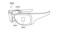
- 210000005252 bulbus oculi Anatomy 0.000 description 10
- 238000002674 endoscopic surgery Methods 0.000 description 10
- 238000003384 imaging method Methods 0.000 description 10
- 239000012212 insulator Substances 0.000 description 10
- 239000012535 impurity Substances 0.000 description 9
- 238000004364 calculation method Methods 0.000 description 8
- 229910052751 metal Inorganic materials 0.000 description 8
- 239000002184 metal Substances 0.000 description 8
- 210000001519 tissue Anatomy 0.000 description 7
- 238000007781 pre-processing Methods 0.000 description 6
- 230000007704 transition Effects 0.000 description 6
- 230000005856 abnormality Effects 0.000 description 5
- 230000008859 change Effects 0.000 description 5
- 238000004891 communication Methods 0.000 description 5
- 238000005516 engineering process Methods 0.000 description 5
- 210000003128 head Anatomy 0.000 description 5
- 230000015556 catabolic process Effects 0.000 description 4
- 230000005284 excitation Effects 0.000 description 4
- 239000000463 material Substances 0.000 description 4
- 239000004984 smart glass Substances 0.000 description 4
- WFKWXMTUELFFGS-UHFFFAOYSA-N tungsten Chemical compound [W] WFKWXMTUELFFGS-UHFFFAOYSA-N 0.000 description 4
- 229910052721 tungsten Inorganic materials 0.000 description 4
- 239000010937 tungsten Substances 0.000 description 4
- 230000000007 visual effect Effects 0.000 description 4
- 230000007274 generation of a signal involved in cell-cell signaling Effects 0.000 description 3
- 239000011521 glass Substances 0.000 description 3
- 230000004888 barrier function Effects 0.000 description 2
- 210000004204 blood vessel Anatomy 0.000 description 2
- 239000000969 carrier Substances 0.000 description 2
- 239000003153 chemical reaction reagent Substances 0.000 description 2
- 238000010276 construction Methods 0.000 description 2
- 238000012937 correction Methods 0.000 description 2
- 230000008878 coupling Effects 0.000 description 2
- 238000010168 coupling process Methods 0.000 description 2
- 238000005859 coupling reaction Methods 0.000 description 2
- 230000007547 defect Effects 0.000 description 2
- 238000011161 development Methods 0.000 description 2
- 230000009977 dual effect Effects 0.000 description 2
- MOFVSTNWEDAEEK-UHFFFAOYSA-M indocyanine green Chemical compound [Na+].[O-]S(=O)(=O)CCCCN1C2=CC=C3C=CC=CC3=C2C(C)(C)C1=CC=CC=CC=CC1=[N+](CCCCS([O-])(=O)=O)C2=CC=C(C=CC=C3)C3=C2C1(C)C MOFVSTNWEDAEEK-UHFFFAOYSA-M 0.000 description 2
- 229960004657 indocyanine green Drugs 0.000 description 2
- 239000011229 interlayer Substances 0.000 description 2
- 230000001678 irradiating effect Effects 0.000 description 2
- 238000002955 isolation Methods 0.000 description 2
- 238000010801 machine learning Methods 0.000 description 2
- 230000001179 pupillary effect Effects 0.000 description 2
- 230000009467 reduction Effects 0.000 description 2
- 238000001028 reflection method Methods 0.000 description 2
- VZSRBBMJRBPUNF-UHFFFAOYSA-N 2-(2,3-dihydro-1H-inden-2-ylamino)-N-[3-oxo-3-(2,4,6,7-tetrahydrotriazolo[4,5-c]pyridin-5-yl)propyl]pyrimidine-5-carboxamide Chemical compound C1C(CC2=CC=CC=C12)NC1=NC=C(C=N1)C(=O)NCCC(N1CC2=C(CC1)NN=N2)=O VZSRBBMJRBPUNF-UHFFFAOYSA-N 0.000 description 1
- YLZOPXRUQYQQID-UHFFFAOYSA-N 3-(2,4,6,7-tetrahydrotriazolo[4,5-c]pyridin-5-yl)-1-[4-[2-[[3-(trifluoromethoxy)phenyl]methylamino]pyrimidin-5-yl]piperazin-1-yl]propan-1-one Chemical compound N1N=NC=2CN(CCC=21)CCC(=O)N1CCN(CC1)C=1C=NC(=NC=1)NCC1=CC(=CC=C1)OC(F)(F)F YLZOPXRUQYQQID-UHFFFAOYSA-N 0.000 description 1
- NIPNSKYNPDTRPC-UHFFFAOYSA-N N-[2-oxo-2-(2,4,6,7-tetrahydrotriazolo[4,5-c]pyridin-5-yl)ethyl]-2-[[3-(trifluoromethoxy)phenyl]methylamino]pyrimidine-5-carboxamide Chemical compound O=C(CNC(=O)C=1C=NC(=NC=1)NCC1=CC(=CC=C1)OC(F)(F)F)N1CC2=C(CC1)NN=N2 NIPNSKYNPDTRPC-UHFFFAOYSA-N 0.000 description 1
- AFCARXCZXQIEQB-UHFFFAOYSA-N N-[3-oxo-3-(2,4,6,7-tetrahydrotriazolo[4,5-c]pyridin-5-yl)propyl]-2-[[3-(trifluoromethoxy)phenyl]methylamino]pyrimidine-5-carboxamide Chemical compound O=C(CCNC(=O)C=1C=NC(=NC=1)NCC1=CC(=CC=C1)OC(F)(F)F)N1CC2=C(CC1)NN=N2 AFCARXCZXQIEQB-UHFFFAOYSA-N 0.000 description 1
- MCMNRKCIXSYSNV-UHFFFAOYSA-N ZrO2 Inorganic materials O=[Zr]=O MCMNRKCIXSYSNV-UHFFFAOYSA-N 0.000 description 1
- 230000004913 activation Effects 0.000 description 1
- 238000013528 artificial neural network Methods 0.000 description 1
- 230000008901 benefit Effects 0.000 description 1
- 238000007906 compression Methods 0.000 description 1
- 230000006835 compression Effects 0.000 description 1
- 210000004087 cornea Anatomy 0.000 description 1
- 230000007423 decrease Effects 0.000 description 1
- 230000003111 delayed effect Effects 0.000 description 1
- 230000006866 deterioration Effects 0.000 description 1
- 230000000694 effects Effects 0.000 description 1
- 238000010336 energy treatment Methods 0.000 description 1
- CJNBYAVZURUTKZ-UHFFFAOYSA-N hafnium(iv) oxide Chemical compound O=[Hf]=O CJNBYAVZURUTKZ-UHFFFAOYSA-N 0.000 description 1
- 238000010030 laminating Methods 0.000 description 1
- 230000031700 light absorption Effects 0.000 description 1
- 210000004400 mucous membrane Anatomy 0.000 description 1
- BPUBBGLMJRNUCC-UHFFFAOYSA-N oxygen(2-);tantalum(5+) Chemical compound [O-2].[O-2].[O-2].[O-2].[O-2].[Ta+5].[Ta+5] BPUBBGLMJRNUCC-UHFFFAOYSA-N 0.000 description 1
- RVTZCBVAJQQJTK-UHFFFAOYSA-N oxygen(2-);zirconium(4+) Chemical compound [O-2].[O-2].[Zr+4] RVTZCBVAJQQJTK-UHFFFAOYSA-N 0.000 description 1
- 230000002093 peripheral effect Effects 0.000 description 1
- 210000001747 pupil Anatomy 0.000 description 1
- 238000007789 sealing Methods 0.000 description 1
- 238000001356 surgical procedure Methods 0.000 description 1
- 230000002194 synthesizing effect Effects 0.000 description 1
- 238000012549 training Methods 0.000 description 1
Images


Classifications
-
- H—ELECTRICITY
- H01—ELECTRIC ELEMENTS
- H01L—SEMICONDUCTOR DEVICES NOT COVERED BY CLASS H10
- H01L21/00—Processes or apparatus adapted for the manufacture or treatment of semiconductor or solid state devices or of parts thereof
- H01L21/02—Manufacture or treatment of semiconductor devices or of parts thereof
- H01L21/04—Manufacture or treatment of semiconductor devices or of parts thereof the devices having at least one potential-jump barrier or surface barrier, e.g. PN junction, depletion layer or carrier concentration layer
- H01L21/18—Manufacture or treatment of semiconductor devices or of parts thereof the devices having at least one potential-jump barrier or surface barrier, e.g. PN junction, depletion layer or carrier concentration layer the devices having semiconductor bodies comprising elements of Group IV of the Periodic System or AIIIBV compounds with or without impurities, e.g. doping materials
- H01L21/30—Treatment of semiconductor bodies using processes or apparatus not provided for in groups H01L21/20 - H01L21/26
- H01L21/31—Treatment of semiconductor bodies using processes or apparatus not provided for in groups H01L21/20 - H01L21/26 to form insulating layers thereon, e.g. for masking or by using photolithographic techniques; After treatment of these layers; Selection of materials for these layers
- H01L21/3205—Deposition of non-insulating-, e.g. conductive- or resistive-, layers on insulating layers; After-treatment of these layers
-
- H—ELECTRICITY
- H01—ELECTRIC ELEMENTS
- H01L—SEMICONDUCTOR DEVICES NOT COVERED BY CLASS H10
- H01L21/00—Processes or apparatus adapted for the manufacture or treatment of semiconductor or solid state devices or of parts thereof
- H01L21/70—Manufacture or treatment of devices consisting of a plurality of solid state components formed in or on a common substrate or of parts thereof; Manufacture of integrated circuit devices or of parts thereof
- H01L21/71—Manufacture of specific parts of devices defined in group H01L21/70
- H01L21/768—Applying interconnections to be used for carrying current between separate components within a device comprising conductors and dielectrics
-
- H—ELECTRICITY
- H01—ELECTRIC ELEMENTS
- H01L—SEMICONDUCTOR DEVICES NOT COVERED BY CLASS H10
- H01L23/00—Details of semiconductor or other solid state devices
- H01L23/52—Arrangements for conducting electric current within the device in operation from one component to another, i.e. interconnections, e.g. wires, lead frames
- H01L23/522—Arrangements for conducting electric current within the device in operation from one component to another, i.e. interconnections, e.g. wires, lead frames including external interconnections consisting of a multilayer structure of conductive and insulating layers inseparably formed on the semiconductor body
-
- H—ELECTRICITY
- H01—ELECTRIC ELEMENTS
- H01L—SEMICONDUCTOR DEVICES NOT COVERED BY CLASS H10
- H01L27/00—Devices consisting of a plurality of semiconductor or other solid-state components formed in or on a common substrate
- H01L27/14—Devices consisting of a plurality of semiconductor or other solid-state components formed in or on a common substrate including semiconductor components sensitive to infrared radiation, light, electromagnetic radiation of shorter wavelength or corpuscular radiation and specially adapted either for the conversion of the energy of such radiation into electrical energy or for the control of electrical energy by such radiation
- H01L27/144—Devices controlled by radiation
- H01L27/146—Imager structures
Definitions
- a photoelectric conversion device includes a pixel array configured such that pixels including a plurality of avalanche photodiodes (hereinafter referred to as APDs) are arranged in a planar two-dimensional array.
- APDs avalanche photodiodes
- the Geiger mode operates with a potential difference between the anode and cathode greater than the breakdown voltage
- the linear mode operates with a voltage difference near or below the breakdown voltage between the anode and cathode. mode.
- an APD operated in Geiger mode is called a SPAD (Single Photon Avalanche Diode).
- Patent Document 1 discloses a SPAD sensor in which a first substrate and a second substrate are laminated, the first substrate having an APD, and the second substrate having a signal processing circuit for processing signals from the APD. is disclosed. Further, in Patent Document 1, a counter circuit for counting the number of incident photons is provided.
- a photoelectric conversion device includes: a first semiconductor layer including a plurality of photoelectric conversion units; a first substrate having a first wiring structure including at least one wiring layer; and a second substrate having a second wiring structure with a plurality of wiring layers, the plurality of photoelectric conversion units has an avalanche photodiode, and the first substrate such that the first wiring structure and the second wiring structure are provided between the first semiconductor layer and the second semiconductor layer.
- the first wiring structure or the second wiring structure has a pad electrode for supplying a voltage to the avalanche photodiode, and the plurality of wiring layers of the second wiring structure is arranged with a first wiring for supplying a power supply voltage to the plurality of pixel circuits, and a wiring layer having the largest area occupied by the first wiring among the plurality of wiring layers; and the first wiring.
- the first wiring has both ends in a first direction of a region in which each of the plurality of pixel circuits is provided and both ends in a second direction crossing the first direction, depending on the combination of the wiring layer groups. It is characterized by being configured to be connected.
- FIG. 4 is a diagram schematically showing the relationship between the operation of the APD and the output signal;
- Cross-sectional view of a photoelectric conversion device FIG. 2 is a diagram showing a wiring layout of power supply voltages according to the first embodiment;
- FIG. 2 is a diagram showing a wiring layout of power supply voltages according to the first embodiment;
- FIG. 2 is a diagram showing a wiring layout of power supply voltages according to the first embodiment;
- FIG. 10 is a diagram showing a wiring layout of the power supply voltage of the second embodiment;
- FIG. 10 is a diagram showing a wiring layout of the power supply voltage of the second embodiment;
- FIG. 10 is a diagram showing a wiring layout of the power supply voltage of the second embodiment;
- FIG. 10 is a diagram showing a wiring layout of the power supply voltage of the second embodiment;
- FIG. 10 is a diagram showing a wiring layout of the power supply voltage of the second embodiment;
- FIG. 10 is a diagram showing a wiring layout of the power supply voltage of the second embodiment;
- FIG. 10 is a diagram showing a wiring layout of the power supply voltage of the second embodiment;
- FIG. 10 is a diagram showing the layout of the pixel circuit of Embodiment 3;
- FIG. 10 is a diagram showing the layout of the pixel circuit of Embodiment 3;
- FIG. 10 is a diagram showing the layout of the pixel circuit of Embodiment 4;
- FIG. 10 is a diagram showing the layout of the pixel circuit of Embodiment 4;
- FIG. 10 is a diagram showing the layout of the pixel circuit of Embodiment 4;
- FIG. 10 is a diagram showing the layout of the pixel circuit of Embodiment 4;
- FIG. 10 is a diagram showing the layout of the pixel circuit of Embodiment 4;
- FIG. 10 is a diagram showing the layout of the pixel
- FIG. 10 is a diagram showing the layout of the pixel circuit of Embodiment 4;
- FIG. 10 is a diagram showing the layout of the pixel circuit of Embodiment 4;
- FIG. 11 shows the configuration and wiring layout of the photoelectric conversion device of Embodiment 5;
- FIG. 11 shows the configuration and wiring layout of the photoelectric conversion device of Embodiment 5;
- FIG. 11 shows the configuration and wiring layout of the photoelectric conversion device of Embodiment 5;
- FIG. 11 shows the configuration and wiring layout of a photoelectric conversion device according to Embodiment 6;
- FIG. 11 shows the configuration and wiring layout of a photoelectric conversion device according to Embodiment 6;
- FIG. 11 shows the configuration and wiring layout of a photoelectric conversion device according to Embodiment 6;
- FIG. 11 shows the configuration and wiring layout of a photoelectric conversion device according to Embodiment 6;
- FIG. 11 shows the configuration and wiring layout of a photoelectric conversion device according to Embodiment 6;
- FIG. 11 shows
- FIG. 11 shows the configuration and wiring layout of a photoelectric conversion device according to Embodiment 6; Modified Example 1 of Cross-Sectional View of Photoelectric Conversion Device Modified Example 2 of Cross-Sectional View of Photoelectric Conversion Device Modified Example 2 of Cross-Sectional View of Photoelectric Conversion Device Modified Example 2 of Cross-Sectional View of Photoelectric Conversion Device Functional block diagram of the photoelectric conversion system of Embodiment 7 Functional block diagram of the distance sensor of Embodiment 8 Functional block diagram of endoscopic surgery of Embodiment 9
- FIG. 11 is a diagram of a photoelectric conversion system and a moving object according to Embodiment 10;
- FIG. 11 is a diagram of a photoelectric conversion system and a moving object according to Embodiment 10;
- Functional block diagram of endoscopic surgery according to Embodiment 11 Functional block diagram of endoscopic surgery according to Embodiment 11
- a photoelectric conversion device including a SPAD (Single Photon Avalanche Diode) that counts the number of photons incident on an avalanche diode.
- a photoelectric conversion device may include at least an avalanche diode, and may be operated in a linear mode as well as a Geiger mode.
- the anode of the avalanche diode is set to a fixed potential and the signal is extracted from the cathode side. Therefore, the semiconductor region of the first conductivity type in which majority carriers are the same conductivity type as the signal charges is the N-type semiconductor region, and the semiconductor region of the second conductivity type is the P-type semiconductor region.
- the present invention can also be applied when the cathode of the avalanche diode is set at a fixed potential and the signal is extracted from the anode side.
- the semiconductor region of the first conductivity type having majority carriers of the same conductivity type as the signal charge is a P-type semiconductor region
- the semiconductor region of the second conductivity type is an N-type semiconductor region.
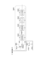
- FIG. 1 is a diagram showing an overall image of a photoelectric conversion device 100.
- the first substrate 11 is also called a sensor chip, and is provided with a pixel region 12 in which pixels having photoelectric conversion units are arranged two-dimensionally.
- a peripheral region 13 is provided between the pixel region 12 and the chip edge of the photoelectric conversion device 100 .
- the second substrate 21 is also called a pixel circuit chip, and is provided with a signal processing circuit area 22 for processing signals from the photoelectric conversion section.
- the photoelectric conversion device 100 is configured by stacking the first substrate 11 and the second substrate 21 . Although not shown, it is also possible to further laminate a third substrate on the laminate of the first substrate and the second substrate.
- the pixels 101 are typically pixels for forming an image, but when used for TOF (Time of Flight), they do not necessarily form an image. That is, the pixel 101 may be an element for measuring the time and amount of light that light reaches.
- TOF Time of Flight
- FIG. 3A is a configuration diagram of the second substrate 21.
- the second substrate 21 is provided with a plurality of signal processing units 103 that process signals photoelectrically converted by the photoelectric conversion units 102 .
- the plurality of signal processing units 103 are provided in the signal processing circuit area 22 arranged two-dimensionally.
- the signal processing unit 103 is also a pixel circuit arranged corresponding to each pixel.
- the signal processing unit 103 is provided with a counter, a memory, and the like, and a digital value is held in the memory.
- a signal output from the signal processing unit 103 is transmitted to a signal line 113 using a vertical scanning circuit 110 and a horizontal scanning circuit 111 .
- FIG. 4 is a diagram illustrating in more detail the block diagrams described in FIGS. 2 and 3A and 3B.
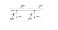
- a voltage VPDL (first voltage) is supplied to the anode of the APD 3100 .
- the cathode of the APD 3100 is supplied with a voltage VDD (second voltage) higher than the voltage VPDL supplied to the anode.
- a reverse bias voltage is supplied to the anode and cathode so that the APD 3100 performs an avalanche multiplication operation.
- charges generated by the incident light undergo avalanche multiplication, generating an avalanche current.
- the Geiger mode is a mode in which the potential difference between the anode and cathode is greater than the breakdown voltage.
- a linear mode is a mode in which the potential difference between the anode and cathode is close to or less than the breakdown voltage.
- an APD operated in the Geiger mode is called a SPAD.
- the voltage VPDL (first voltage) is -30V
- the voltage VDD (second voltage) is 1V.
- the potential difference between 0 V which is the voltage VSS (third voltage)
- the voltage VPDL (first voltage) is greater than the potential difference between the voltage VSS (third voltage) and the voltage VH (second voltage). Therefore, the voltage VPDL (first voltage) is sometimes expressed as a high voltage.
- the quenching element 3010 is connected to the power supply supplying the voltage VDD and the APD 3100 .
- the quench element 3010 has the function of converting the change in avalanche current generated by the APD 3100 into a voltage signal.
- the quench element 3010 functions as a load circuit (quench element) during signal multiplication by avalanche multiplication, suppresses the voltage supplied to the APD 3100, and has a function of suppressing avalanche multiplication (quench operation).
- a waveform shaping circuit 3020 shapes the potential change of the cathode of the APD 3100 obtained during photon detection, and outputs a pulse signal.
- the waveform shaping circuit 3020 for example, an inverter circuit is used.
- the waveform shaping circuit 212 may use one inverter, a circuit in which a plurality of inverters are connected in series, or other circuits having waveform shaping effects.
- the processing circuit 3030 is a circuit that performs arbitrary signal processing.
- the processing circuit 3030 is a circuit that selects whether or not to input the signal output from the waveform shaping circuit 3020 to the counter circuit 3040 . More specifically, during the exposure period, the processing circuit 3030 is configured to input the pulse signal output from the waveform shaping circuit 3020 to the counter circuit 3040 . On the other hand, during the non-exposure period, the processing circuit 3030 is configured not to input the pulse signal to the counter circuit 3040 even if the pulse signal is output from the waveform shaping circuit 3020 . By the way, in order to set the exposure period and the non-exposure period, it is possible to switch between these periods by controlling the quench element 3010 as described later. If the processing circuit 3030 described above is provided, it is possible to control the exposure period and the non-exposure period without depending on the control of the quench element 3010 .
- the counter circuit 3040 counts the pulse signals output from the waveform shaping circuit 3020 and holds the count value. When a control pulse pRES is supplied via a drive line (not shown), the signal held in the counter circuit 3040 is reset.
- the counter circuit 3040 provided for each pixel has a large circuit scale. Therefore, a configuration having a third substrate may be employed, and in addition to providing the counter circuit 3040 on the second substrate 21, part of the counter circuit 3040 may also be provided on the third substrate.
- the quench element 3010 is composed of a MOS transistor, and a clock period pulse may be applied to the gate of this MOS transistor.
- a pulse having a predetermined clock period is input to the gate of the quench element 3010 from a PLL (Phase Locked Loop) circuit (not shown).
- PLL Phase Locked Loop
- the quenching element 3010 is PMOS, so the quenching element 3010 is turned off.
- APD 3100 is not recharged and is in non-detection mode.
- a voltage VDD (second voltage) and a voltage VSS (third voltage) are supplied to the waveform shaping circuit 3020, the processing circuit 3030, the counter circuit 3040, and the output circuit 3050 as drive voltages.
- the counter circuit 3040 is provided has been described above. However, it is also possible to provide a time-to-digital converter (hereinafter referred to as a TDC circuit) as a time measurement circuit without providing the counter circuit. Thus, the photoelectric conversion device 100 that acquires the pulse detection timing is configured.
- a TDC circuit time-to-digital converter
- the generation timing of the pulse signal output from the waveform shaping circuit 3020 is converted into a digital signal by the TDC circuit.
- a control pulse pREF reference signal
- the TDC circuit acquires a signal as a digital signal when the input timing of the signal output from each pixel through the waveform shaping circuit 3020 is relative to the control pulse pREF.
- a TDC circuit has, for example, an RS flip-flop, a coarse counter, and a fine counter.
- the drive pREF drives the light-emitting portion and sets the RS flip-flop, which is reset by a signal pulse input from each pixel. Thereby, a signal having a pulse width corresponding to the flight time of light is generated. The generated signal is counted by a coarse counter and a fine counter each having a predetermined time resolution. As a result, a digital code is output.
- a PLL circuit that generates a pulse of drive pREF for the TDC circuit is provided on the first substrate 11 or the second substrate 21, or on both the first substrate 11 and the second substrate 21.
- the driving pREF pulse input to the TDC circuit is delayed, it will affect the accuracy of the information output from the TDC circuit. Therefore, it is better to provide the PLL circuit on the same substrate as the substrate on which the TDC circuit is provided.
- the second substrate 21 is provided with a TDC circuit and a PLL circuit.
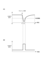
- FIG. 5 is a diagram schematically showing the relationship between the operation of the APD and the output signal.
- nodeA be the Vcath on the input side of the waveform shaping circuit 3020
- nodeB be the output side.
- FIG. 5A shows waveform changes of nodeA in FIG. 4
- FIG. 5B shows waveform changes of nodeB in FIG.
- a potential difference capable of avalanche multiplication is applied between times t0 and t1.
- an avalanche multiplication current flows through quench element 3010, and the voltage of nodeA drops.
- the avalanche multiplication of APD 3100 stops, and the voltage level of nodeA does not drop beyond a certain value.
- a current that compensates for the voltage drop from the voltage VPDL flows through the nodeA, and the nodeA is stabilized at the original potential level at the time t3.
- the portion of the output waveform at nodeA that exceeds a certain threshold is shaped by the waveform shaping circuit 3020 and output as a signal from nodeB.
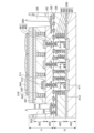
- the first substrate 11 is composed of a first substrate semiconductor layer 302 (first semiconductor layer) and a first substrate wiring structure 303 (first wiring structure).
- the second substrate 21 is composed of a second substrate semiconductor layer 402 (second semiconductor layer) and a second substrate wiring structure 403 (second wiring structure).
- the first substrate 11 and the second substrate 21 are bonded so that the first wiring structure 303 and the second wiring structure 403 face each other and are in contact with each other.
- a first conductivity type first semiconductor region 311 and a second conductivity type second semiconductor region 316 are arranged in the first semiconductor layer 302 to form a PN junction to form the APD 3100 shown in FIG. ing.
- Each pixel is separated by a second conductivity type fourth semiconductor region 314 .
- a fifth semiconductor region 315 of the second conductivity type is provided on the light incident surface side of the fourth semiconductor region 314 .
- the fifth semiconductor region 315 is provided in common for each pixel.
- a pinning layer 341 is provided on the light incident surface side of the fifth semiconductor region 315 .
- the pinning layer 341 is a layer arranged for suppressing dark current.
- the pinning layer 341 is formed using hafnium oxide (HfO 2 ), for example.
- the pinning layer 341 may be formed using zirconium dioxide (ZrO 2 ), tantalum oxide (Ta 2 O 5 ), or the like.
- a microlens 344 is provided on the pinning layer 341 via an insulating layer 342 and a color filter 343 .
- the insulating layer 342 and the color filter 343 have arbitrary configurations.
- a grid-shaped light shielding film or the like may be provided between the microlens 344 and the pinning layer 341, for optically separating each pixel.
- any material can be used as long as it can shield light. For example, tungsten (W), aluminum (Al), copper (Cu), or the like can be used.
- the second semiconductor layer is provided with an active region 411 made of a semiconductor region and an isolation region 412 .
- Isolation region 412 is a field region made of an insulator.
- a first junction 385 is provided on the uppermost layer of the first wiring structure 303 so as to be exposed from the first wiring structure 303 .
- Pad openings 353 (first pad opening) and 355 (second pad opening) are formed in the first wiring structure 303 .
- Pad electrodes 354 and 352 are provided at the bottoms of the pad openings 353 and 355, respectively.
- the pad electrode 352 is an electrode for supplying voltage to the circuit of the first substrate. For example, a voltage VPDL (first voltage) is supplied from the pad electrode 352 to the fourth semiconductor region 314 via via wiring (not shown) or contact wiring (not shown).
- the bonding between the first bonding portion 385 exposed on the bonding surface of the first substrate and the second bonding portion 395 exposed on the bonding surface of the second substrate is a metal bonding (MB) structure, or metal bonding. It is also called a department. Since this bonding is often performed between copper (Cu), it is also called Cu--Cu bonding (Cu--Cu bonding).
- the pad electrode 354 provided on the first wiring structure 303 is electrically connected to any one of the plurality of wirings provided on the plurality of wiring layers 390 via the first joint portion 385 and the second joint portion 395. It is connected.
- the voltage VSS third voltage
- a voltage VDD second voltage
- a voltage is supplied to the wiring of the plurality of wiring layers 390 through the first joint portion 385 and the second joint portion 395 , and the voltage is supplied through the second joint portion 395 and the first joint portion 385 .
- FIG. 7 is a diagram showing the wiring arrangement of the voltage VDD (second voltage) shown in FIG.
- the APD sensor including the SPAD has a large number of circuits forming the pixel circuit 3000 provided for each pixel. For this reason, there are many power supply wirings to each circuit and many input/output wirings to each circuit, and the wiring density between circuits increases. As the wiring density increases, the wiring for voltage VDD (second voltage) and voltage VSS (third voltage), which are power supplies to each circuit, is likely to be cut off, which is a reason for hindering stable current supply.
- "dividing" means that power supply wiring is not arranged in a two-dimensional direction in a certain wiring layer.
- disposing the wiring of the power supply in two-dimensional directions means that the wiring is disposed so as to reach both ends in the first direction and both ends in the second direction in the region where the pixel circuit for one pixel is provided. is that This is because if the wiring is not arranged in this way, the wiring between the pixel circuits of adjacent pixels will not be electrically connected when the pixel circuits for a plurality of pixels are laid out.
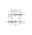
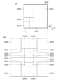
- FIG. 7A shows an arrangement example of the wiring 1010 of the voltage VDD (second voltage) provided in the first wiring layer (M1) in plan view.
- FIG. 7B shows the arrangement of wiring 1020 for voltage VDD (second voltage) provided in the second wiring layer (M2) in plan view.
- the wiring 1010 is arranged extending in the second direction 40 . Specifically, in a region where a pixel circuit for one pixel is provided, the wiring 1010 is arranged extending in the second direction 40 from ends 41 to ends 42 which are both ends of the region. there is On the other hand, the wiring 1010 is not arranged to extend in the first direction 30 that intersects (here, the direction orthogonal to) the second direction 40 .
- the first wiring layer (M1) wirings for connecting circuits constituting pixel circuits, gate wirings, and the like are arranged at high density. Therefore, in the first wiring layer (M1), another wiring becomes an obstacle, and the wiring 1010 cannot be extended in the first direction 30.
- FIG. 1 wirings for connecting circuits constituting pixel circuits, gate wirings, and the like are arranged at high density. Therefore, in the first wiring layer (M1), another wiring becomes an obstacle, and the wiring 1010 cannot be extended in the first direction 30.
- both ends in the first direction 30 are connected to the wirings 1020 of the second wiring layer, and both ends in the second direction 40 are connected to the wirings 1010 of the first wiring layer. is connected. That is, by combining the wirings of the two wiring layers, both ends in the first direction and both ends in the second direction are connected in a plan view with respect to the region in which the pixel circuit for one pixel is provided.
- the wiring density is increased, and even if the wiring for the power supply voltage cannot be arranged two-dimensionally by using only one wiring layer, the power supply wiring can be arranged two-dimensionally. becomes. Therefore, when a first pixel that consumes a large amount of current and a second pixel that consumes a small amount of current are adjacent to each other, even if a large amount of current is consumed from the power wiring of the pixel circuit of the first pixel, the power supply of the pixel circuit of the second pixel is A current can be supplied from the wiring to the pixel circuit of the first pixel. This allows stable current supply to the pixel circuit.
- FIG. 7(C) shows an example in which two wiring layers are used for one pixel, and wiring is arranged so as to extend in both the first direction 30 and the second direction 40 .
- FIG. 7D shows four pixels.
- the wiring layout of each pixel is symmetrical with respect to the boundary line of each pixel. Such an arrangement is also called a mirror symmetrical arrangement.
- other pixels adjacent to the four pixels shown are also arranged in such line symmetry.
- the area where the pixel circuit for one pixel is provided is also the area where the predetermined wiring pattern is repeated.
- FIG. 7D shows an example of a mirror-symmetrical arrangement, but even in such a mirror-symmetrical arrangement, regions where pixel circuits for one pixel are provided are repeated.
- FIG. 7D shows an example of a mirror symmetrical arrangement, a translational symmetrical arrangement may be used. Also in this case, the regions where the pixel circuits for one pixel are provided are repeated.
- the horizontal direction is the first direction and the vertical direction is the second direction with respect to the paper surface, but the vertical direction may be the first direction and the horizontal direction may be the second direction.
- Figs. 8(A) and (B) are the same as Figs. 7(A) and (B), so the description is omitted.
- FIG. 8(C) is a diagram showing wiring 1040 for supplying voltage VDD (second voltage) provided in the third wiring layer (M3).
- VDD second voltage
- the wiring 1040 provided in the third wiring layer (M3) and the wiring 1020 provided in the second wiring layer (M2) are electrically connected by a via wiring 1050. ing.
- the wiring 1040 of the third wiring layer (M3) is only the third wiring layer (M3), and both ends in the first direction and both ends in the second direction are flat. visually connected.
- FIG. 8(E) shows four pixels arranged mirror-symmetrically.
- the wiring width of the wiring placed in the wiring layer farthest from the semiconductor layer is placed in the wiring layer closer to the semiconductor layer (lower wiring layer). It is possible to make it wider than the wiring width of the wiring to be used. That is, the third wiring layer (M3) is the wiring layer in which the wiring of the voltage VDD (second voltage) occupies the largest area among the plurality of wiring layers. As a result, as shown in FIG. 8C, the wiring width of the wiring for supplying the voltage VDD (second voltage) provided in the third wiring layer (M3) is increased to reduce the resistance. .
- the wiring for supplying the voltage VDD (second voltage) provided in the third wiring layer (M3) extends so that both ends in the first direction 30 and both ends in the second direction 40 are connected. and distributed.
- the distance between the third wiring layer (M3) and the second semiconductor layer 402 in which the pixel circuit is provided varies depending on the distance between the second wiring layer (M2) and the second semiconductor layer 402 and the distance between the first wiring layer (M2) and the second semiconductor layer 402. longer than the distance between the layer (M1) and the second semiconductor layer 402; Therefore, with only the third wiring layer (M3), the current supply from the pixel circuit of the pixel with low current consumption to the pixel circuit of the pixel with high current consumption may be insufficient. Therefore, even in such a case, the power wiring is two-dimensionally arranged by combining the first wiring layer (M1) and the second wiring layer (M2). This allows stable current supply to the pixel circuit.
- the first wiring layer (M1) and the second wiring layer (M2) are a plurality of wiring layers provided between the wiring layer occupying the largest wiring area and the second semiconductor layer 402. Therefore, it is sometimes called a lower wiring layer group. Alternatively, it may simply be called a wiring layer group.
- FIG. 9 is a diagram showing wirings provided in the first wiring layer (M1) to the third wiring layer (M3). Since FIG. 9C is the same as FIG. 8C, description thereof is omitted.
- FIG. 9A is a diagram showing wiring 1010 for supplying voltage VDD (second voltage) provided in the first wiring layer (M1).
- VDD second voltage
- the wiring 1010 extends in the second direction 40 so as to reach both ends in the second direction 40 of the region where the pixel circuit for one pixel is provided.
- FIG. 9A is different in that the region does not reach both ends in the first direction 30 and neither ends in the second direction 40 .
- FIG. 9B is a diagram showing wiring 1020 for supplying voltage VDD (second voltage) provided in the second wiring layer (M2). As in FIG. 8B, also in FIG. 9B, the wiring 1020 extends in the first direction so as to reach both ends in the first direction 30 of the region where the pixel circuit for one pixel is provided. exist. In addition, in FIG. 9B, a wiring 1025 extending also in the second direction 40 is provided in the region.
- VDD second voltage
- M2 second wiring layer
- the region in the two-dimensional direction is No wiring is provided to connect to both ends.
- the wiring is configured such that both ends of the region in the first direction and both ends in the second direction are connected.
- the first wiring layer (M1) is provided with wiring so as to be connected to both ends of the region in which the pixel circuit for one pixel is provided.
- wiring in the second wiring layer (M2) wiring was provided so as to be connected to both ends of the region in which the pixel circuit for one pixel was provided.
- the wiring provided in the first wiring layer (M1) is connected to one end of the region in which the pixel circuit for one pixel is provided, and is connected to the other end.
- a non-connected configuration is also possible.
- FIGS. May be arranged as shown.
- the voltage VDD second voltage
- the third wiring layer (M3) and the fourth wiring layer (M2) are closer to the first substrate 11 than the second wiring layer (M2).
- M4 may be used to two-dimensionally arrange the power wiring.
- all of the first wiring layer (M1) to the third wiring layer (M3) may be used to arrange the power wiring two-dimensionally.
- the wiring combined by the wiring layer group was a two-dimensional wiring consisting of two straight lines.
- the wiring is arranged so as to reach both ends in the first direction and both ends in the second direction of the region in which the pixel circuit for one pixel is provided, as long as this condition is satisfied, after combining , may have more complex shapes.
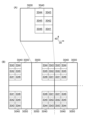
- FIG. 10A to 10C are diagrams showing the wiring layout of the voltage VDD (second voltage) shown in FIG.
- the APD sensor including the SPAD has a large number of circuits forming the pixel circuit 3000 provided for each pixel. For this reason, there are many power supply wirings to each circuit and many input/output wirings to each circuit, and the wiring density between circuits increases. As the wiring density increases, the wiring for voltage VDD (second voltage) and voltage VSS (third voltage), which are power supplies to each circuit, is likely to be disconnected, which is a reason for hindering stable current supply.
- FIGS. 10A to 10C show a region in which a pixel circuit for one pixel is provided in the pixel circuit 3000 of the second substrate 21.
- FIG. 10D shows a region where FIGS. 10A to 10C are superimposed.
- FIG. 10A shows an arrangement example of wiring 1110 for voltage VDD (second voltage) and wiring 1115 for voltage VSS (third voltage) provided in the first wiring layer (M1) in plan view.
- the wirings 1110 and 1115 are arranged extending in the second direction 40 to both ends of the region in the second direction 40 . This is because the wirings and gate wirings that connect the circuits forming the pixel circuit are arranged at a high density, so that the wirings cannot be arranged in a two-dimensional direction.
- FIG. 10B shows the arrangement of wiring 1120 for voltage VDD (second voltage) and wiring 1025 for voltage VSS (third voltage) provided in the second wiring layer (M2) in plan view.
- the wirings 1120 and 1125 are arranged extending from one end of the region in the first direction 30, but do not reach the other end of the region. This is because the wirings and gate wirings that connect the circuits that make up the pixel circuit are arranged at high density. This is because wiring cannot be arranged all the way.
- FIG. 10C shows the arrangement of wiring 1140 for voltage VDD (second voltage) and wiring 1145 for voltage VSS (third voltage) provided in the third wiring layer (M3) in plan view.
- the wires 1140 and 1145 are arranged extending in the first direction 30 from the other end of the region, but do not reach one end of the region. This is because the wirings and gate wirings that connect the circuits that make up the pixel circuit are arranged at high density. This is because wiring cannot be arranged all the way.
- the via wiring 1150 electrically connects the wiring 1120 of the voltage VDD (second voltage) of the second wiring layer (M2) and the wiring 1140 of the third wiring layer (M3).
- the wiring 1125 of the voltage VSS (third voltage) of the second wiring layer (M2) and the wiring 1145 of the third wiring layer (M3) are electrically connected by the via wiring 1155 .
- the via wiring 1130 electrically connects the wiring 1110 of the voltage VDD (second voltage) of the first wiring layer (M1) and the wiring 1120 of the voltage VDD of the second wiring layer (M2).
- the wiring 1115 of the voltage VSS (third voltage) of the first wiring layer (M1) and the wiring 1125 of the voltage VSS of the second wiring layer (M2) are electrically connected by the via wiring 1135 .
- the power supply of the pixel circuit of the second pixel is A current can be supplied from the wiring to the pixel circuit of the first pixel. This allows stable current supply to the pixel circuit.
- FIG. 11 is a diagram showing wirings provided in a fourth wiring layer (M4) and a fifth wiring layer (M5), which are wiring layers above the third wiring layer (M3).
- FIGS. 11A to 11C are the same as FIGS. 10A to 10C, description thereof is omitted.
- FIG. 11D illustrates a wiring 1160 for supplying the voltage VSS (third voltage) and a wiring 1165 for supplying the voltage VDD (second voltage) which are provided in the fourth wiring layer (M4).
- Fig. 3 shows an arrangement; A wiring 1160 provided in the fourth wiring layer (M4) and a wiring 1145 provided in the third wiring layer (M3) are electrically connected by a via wiring 1170.
- FIG. 11(F) is the same view as FIG. 11(D).
- FIG. 11G shows four pixels arranged mirror-symmetrically.
- the wiring 1160 provided in the fourth wiring layer (M4) is only the fourth wiring layer (M4), and both ends in the first direction and both ends in the second direction are connected in plan view.
- the fourth wiring layer (M4) is a wiring layer in which wiring of voltage VSS (third voltage) occupies the largest area among the plurality of wiring layers. Thereby, the wiring width of the wiring for supplying the voltage VSS (third voltage) provided in the fourth wiring layer (M4) is increased to reduce the resistance.
- the distance between the fourth wiring layer (M4) and the second semiconductor layer 402 on which the pixel circuit is provided is the same as any wiring layer from the first wiring layer (M1) to the third wiring layer (M3). , and the second semiconductor layer 402 . Therefore, with only the fourth wiring layer (M4), there is a possibility that the current supply from the pixel circuit of the pixel with low current consumption to the pixel circuit of the pixel with high current consumption will be insufficient. Therefore, in the present embodiment, the power wiring is two-dimensionally arranged by combining the first wiring layer (M1) to the third wiring layer (M3). This allows stable current supply to the pixel circuit.
- FIG. 11(E) is a diagram showing the arrangement of wiring 1180 for supplying the voltage VDD (second voltage) provided in the fifth wiring layer (M5).
- the wiring 1180 provided in the fifth wiring layer (M5) and the wiring 1165 provided in the fourth wiring layer (M4) are electrically connected by the via wiring 1190.
- FIG. Also, the wiring 1165 provided in the fourth wiring layer (M4) and the wiring 1140 provided in the third wiring layer (M3) are electrically connected by the via wiring 1175.
- FIG. 11(H) is the same view as FIG. 11(E).
- FIG. 11(I) shows four pixels arranged mirror-symmetrically.
- the wiring 1180 provided in the fifth wiring layer (M5) is only the fifth wiring layer (M5), and both ends in the first direction and both ends in the second direction are connected in plan view.
- the fifth wiring layer (M5) is a wiring layer in which wiring of voltage VDD (second voltage) occupies the largest area among the plurality of wiring layers. As a result, the wiring width of the wiring for supplying the voltage VDD (second voltage) provided in the fifth wiring layer (M5) is increased to reduce the resistance.
- the distance between the fifth wiring layer (M5) and the second semiconductor layer 402 on which the pixel circuit is provided is the same as any wiring layer from the first wiring layer (M1) to the fourth wiring layer (M4). , and the second semiconductor layer 402 . Therefore, with only the fifth wiring layer (M5), the current supply from the pixel circuit of the pixel with low current consumption to the pixel circuit of the pixel with high current consumption may be insufficient. Therefore, in the present embodiment, the power wiring is two-dimensionally arranged by combining the first wiring layer (M1) to the third wiring layer (M3). This allows stable current supply to the pixel circuit.
- the fourth wiring layer (M4) and the fifth wiring layer (M5) are assigned as the wiring layers occupying the largest wiring area for each of the two types of power supply voltages.
- the first wiring layer (M1) to the third wiring layer (M3) are combined to arrange the power wiring two-dimensionally.
- the third wiring layer (M3) and the fifth wiring layer (M5) may be assigned as the wiring layers occupying the largest wiring area.
- the first wiring layer (M1), the second wiring layer (M2), and the fourth wiring layer (M4) may be combined to arrange the power wiring two-dimensionally.
- FIG. 12(A) is an arrangement example of the quench element 3010 and the waveform shaping circuit 3020 included in the pixel circuit 3000 corresponding to one pixel.
- FIG. 12A also shows an arrangement example of the processing circuit 3030, the counter circuit 3040, and the output circuit 3050.
- FIG. A quench element 3010 (for example, it is also called a quench circuit because it is a MOS transistor), a counter circuit 3040, and an output circuit 3050 are provided so as to be in contact with the edge of the pixel. That is, these pixel circuits are arranged so as to be in contact with the boundary between the first pixel and the second pixel adjacent to the first pixel.
- being in contact strictly does not mean being in contact with the edge of a pixel or being in contact with a boundary between pixels, but a circuit having other functions is not arranged between adjacent pixels.
- the circuit closest to the pixel circuit of the second pixel among the pixel circuits of the first pixel is any one of the quench element 301, the counter circuit 3040, and the output circuit 3050 of the first pixel.
- the current can be supplied from the wiring that supplies the voltage to the pixel circuit of the second pixel. easier. Therefore, it is possible to stably supply current to the pixel circuit.
- the quench element 3010 and the waveform shaping circuit 3020 are arranged side by side. As shown in FIG. 4, one node of the MOS transistor that is the quench element 3010 and the input node of the waveform shaping circuit 3020 are electrically connected. Therefore, the quenching element 3010 and the waveform shaping circuit 3020 are arranged close to each other in terms of layout in order to enjoy the merits such as reduction of wiring capacitance.
- FIG. 12B shows an arrangement example of pixel circuits 3000 corresponding to four pixels.
- the pixel circuit of each pixel is arranged in a mirror layout.
- circuits having the same functions as the pixel circuits of the respective pixels are arranged side by side.
- the counter circuits 3040 of the first pixel and the second pixel are adjacent to each other.
- the quench element 3010 and the waveform shaping circuit 3020 of the first pixel and the second pixel are adjacent to each other for the first pixel (upper left pixel) and the second pixel (upper right pixel). This makes it possible to save space when laying out the circuit.
- the quenching element 3010 is arranged at the corner of the region where the pixel circuit is provided.
- the corner portion is arranged at the corner formed by the first side in the first direction 30 and the second side in the second direction 40 of the region where the pixel circuit is provided.
- the corner portion is defined by a side in the first direction 30 and a side in the second direction 40, and a region in which a pixel circuit corresponding to one pixel is provided. It means that it is distributed within
- the quenching element 3010 is positioned within 1/3 of the length of the side from the lower left vertex in the horizontal direction and within 1/3 of the length of the side from the lower left vertex in the vertical direction. is provided.
- the quench element 3010 may be a PMOS transistor, and the transistors forming other circuits may be NMOS transistors.
- the PMOS transistor and the NMOS transistor must have well structures of different conductivity types.
- FIG. 12B it is possible to collectively arrange the quench elements 3010 for four pixels. Therefore, the N-well structure for the quench element 3010 can be shared by four pixels.
- a plurality of pixels it is also possible to arrange a plurality of pixels to share diffusion regions and power wirings (for example, contact wirings).
- FIG. 13A shows a pixel circuit 3000 corresponding to one pixel. Attention is paid to the counter circuit 3040, and circuits other than the counter circuit 3040 are not displayed.
- 3041 is the first bit circuit of the counter.
- 3042, 3043, 3044, 3045, and 3046 are circuits of the 2nd, 3rd, 4th, 5th, and 6th bits of the counter, respectively. Since a 6-bit counter is illustrated here, the 1st bit is the LSB (Least Significant Bit) and the 6th bit is the MSB (Most Significant Bit).
- the area occupied by the counter circuit 3040 in the pixel circuit 3000 is larger than the area occupied by the other circuits.
- the circuits forming the counter circuit 3040 are arranged so as to be folded in the middle to save the space of the pixel circuit 3000 .
- the circuits of the first bit circuit 3041, the second bit circuit 3042, and the third bit circuit 3043 are arranged in the second direction 40 in this order.
- circuit 3044 of the 4th bit is arranged adjacent to the circuit 3043 of the 3rd bit in the first direction 30 .
- the circuit 3044 of the fourth bit, the circuit 3045 of the fifth bit, and the circuit 3046 of the sixth bit are arranged in this order in the direction opposite to the second direction 40 .
- the layout of these circuits is arranged linearly without being folded as described above, the area occupied by the pixel circuit 3000 becomes vertically long or horizontally long.
- the wiring layout of the plurality of photoelectric conversion units 102 arranged on the first substrate 11 and the pixel circuits 3000 arranged corresponding to these photoelectric conversion units 102 may become complicated.
- the space of the pixel circuit 3000 can be saved, and electrical connection between the plurality of photoelectric conversion units 102 and the corresponding pixel circuits 3000 can be achieved. It is also possible to suppress the complication of the wiring layout for the connection relationship.
- FIG. 13(B) shows an example in which pixel circuits 3000 of a total of 6 pixels arranged in 2 rows and 3 columns are arranged.
- FIG. 13B shows the arrangement of the pixel circuits 3000 when a third column is added to the pixel circuits 3000 of four pixels in two rows and two columns shown in FIG. be.
- the counter circuit 3040 of the first pixel is provided so as to be in contact with the edge of the first pixel
- the counter circuit 3040 of the second pixel is provided so as to be in contact with the edge of the second pixel. That is, the counter circuits 3040 of the first and second pixels are arranged so as to be in contact with the boundary between the first and second pixels.
- being in contact strictly does not mean being in contact with the edge of a pixel or being in contact with a boundary between pixels, but a circuit having other functions is not arranged between adjacent pixels.
- a circuit having other functions is not arranged between adjacent pixels.
- no circuit other than the counter circuit is arranged between the counter circuit 3040 of the first pixel and the counter circuit 3040 of the second pixel.
- the shortest distance between the first pixel circuit 3041 (LSB) and the second pixel circuit 3041 (LSB) is the distance between the first pixel circuit 3046 (MSB) and the second pixel circuit 3046 (MSB). shorter than the shortest distance to circuit 3041 (LSB).
- the time during which the LSB circuit is driven is longer than the time during which the MSB circuit is driven, so the LSB circuit consumes more current than the MSB circuit. Therefore, even if the LSB circuit of the first pixel consumes a large amount of current, it is possible to supply the current from the power wiring of the pixel circuit of the second pixel to the pixel circuit of the first pixel.
- the current consumption in the MSB circuit of the first pixel is relatively less than the current consumption in the LSB circuit, such countermeasures are not necessarily required.
- the layout shown in FIG. 13(B) can be described as follows. That is, the counter circuit 3040 of the first pixel and the counter circuit 3040 of the second pixel adjacent to the first pixel are arranged in mirror symmetry (line symmetry). In addition, the LSB circuit 3041 of the first pixel and the LSB circuit 3041 of the second pixel are also arranged in mirror symmetry. The shortest distance between the LSB circuit 3041 of the first pixel and the LSB circuit 3041 of the second pixel is shorter than the shortest distance between the MSB circuit 3046 of the first pixel and the MSB circuit 3046 of the second pixel. By satisfying such a relationship, more stable current can be supplied to the pixel circuit.
- FIG. 14A shows a layout diagram of a pixel circuit 3000 for two pixels in plan view. The focus is on the quenching element 3010, and the circuitry other than the quenching element 3010 is not shown.
- the circuit in the first row and the first column is assumed to be the pixel circuit 3000 of the first pixel, and the circuit in the second row and the first column is assumed to be the pixel circuit 3000 of the second pixel.
- the pixel circuit 3000 of the first pixel and the pixel circuit 3000 of the second pixel are arranged in mirror symmetry (line symmetry).
- FIG. 14B shows a circuit diagram of the quenching element 3010 of the first pixel and the quenching element 3010 of the second pixel.
- VDD second voltage
- one active region is shared by the MOS transistor of the quench element 3010 of the first pixel and the MOS transistor of the quench element 3010 of the second pixel.
- the diffusion region on the source side of the PMOS transistor of the quench element 3010 is shared, and two contact wirings 3015 are provided in the diffusion region. Since the contact wiring 3015 is supplied with the voltage VDD (second voltage), the source of the PMOS transistor of the quench element 3010 is also supplied with the voltage VDD (second voltage).
- the diffusion region which is the source or drain (drain in the case of an NMOS transistor) of the MOS transistor that becomes the quench element 3010, can be shared by the pixel circuits of the two pixels. Thereby, space saving of the pixel circuit can be achieved.
- two contact wirings are provided to connect the shared diffusion region, but one contact wiring may be provided, or three or more contact wirings may be provided.
- the layout can be simplified by sharing one contact wiring between two pixels.
- FIG. 15A shows a layout diagram of a pixel circuit 3000 for two pixels in plan view. Attention is paid to the waveform shaping circuit 3020, and circuits other than the waveform shaping circuit 3020 are not displayed.
- the circuit in the first row and the first column is assumed to be the pixel circuit 3000 of the first pixel, and the circuit in the first row and the second column is assumed to be the pixel circuit 3000 of the second pixel.
- the pixel circuit 3000 of the first pixel and the pixel circuit 3000 of the second pixel are arranged in mirror symmetry (line symmetry).
- FIG. 15B shows a circuit diagram of the waveform shaping circuit 3020 for the first pixel and the waveform shaping circuit 3020 for the second pixel.
- VDD second voltage
- VSS third voltage
- FIG. 15C shows a circuit diagram describing FIG. 15B in more detail.
- the waveform shaping circuit 3020 is composed of an inverter circuit having a PMOS transistor and an NMOS transistor. The input is Vcath and the output is designated Vp.
- the waveform shaping circuit 3020 included in the pixel circuit 3000 of the second pixel has two transistors, one transistor and the other transistor having a common gate.
- a contact wiring 3065 is connected to the gate.
- the contact wiring 3065 is supplied with the voltage Vcath which is the input of the waveform shaping circuit.
- a contact wiring 3035 and a contact wiring 3055 are connected to the source and drain of one transistor (for example, an NMOS transistor) shown in FIG. 15A.
- contact wiring 3025 and contact wiring 3055 are respectively connected to the source and drain of the contact wiring 3035.
- a voltage VSS (third voltage) is supplied to the contact wiring 3035.
- the contact wiring 3015 is supplied with a voltage VDD ( A second voltage) is supplied, and a voltage Vp is output from the contact wiring 3055 .
- the diffusion region connected with the contact wiring 3035 of the waveform shaping circuit 3020 of the first pixel and the diffusion region connected with the contact wiring 3035 of the waveform shaping circuit 3020 of the second pixel are shared. It is
- the diffusion region connected with the contact wiring 3025 of the waveform shaping circuit 3020 of the first pixel and the diffusion region connected with the contact wiring 3025 of the waveform shaping circuit 3020 of the second pixel are shared.
- the diffusion region which is the source or drain of the transistor that constitutes the waveform shaping circuit, can be shared by the pixel circuits of the two pixels. Thereby, space saving of the pixel circuit can be achieved.
- two contact wirings for example, two contact wirings 3025 and two contact wirings 3035
- these two contact wirings may be made common and arranged in a shared diffusion region.
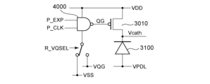
- FIG. 16A shows the APD 3100 and the pixel circuit 3000 for clock driving.
- the quench element 3010, the waveform shaping circuit 3020, the counter circuit 3040, and the signal generation circuit 4000 are shown, and other circuits are omitted.
- the determination threshold of the waveform shaping circuit 3020 is set to a potential higher than the potential difference that causes avalanche multiplication in the APD. Due to the recharge operation, the potential of the nodeA is lower than the determination threshold.
- the signal generation circuit 4000 is composed of a logic circuit.
- the signal generation circuit 4000 is configured by a NAND circuit, and receives a control signal P_EXP for controlling the exposure period and a control signal P_CLK.
- a “0” is output from the logic circuit when the two input signals are “1”. This output is the control signal QG.
- a "1” is output from the logic circuit.
- the control signal QG is "0"
- the quenching element 3010 of the PMOS transistor is turned on, and when the control signal QG is "1", the quenching element 3010 of the PMOS transistor is turned off.
- the control signal P_EXP when the control signal P_EXP is at a high level and the control signal P_CLK is at a high level, the control signal QG is at a low level, and the PMOS transistor, which is the quenching element 3010, goes to a low level. is turned on.
- the quench element 3010 when the quench element 3010 is turned on, the resistance value of the PMOS transistor is lowered and the recharge operation is performed.
- the control signal QG is at high level and the PMOS transistor, which is the quench element 3010, is turned off.
- the quench element 301 is turned off, the resistance of the PMOS transistor increases, making it difficult to perform the recharge operation. Therefore, the APD 3100 stops the avalanche multiplication operation.
- the control signal QG transitions from high level to low level, the quench element 3010 is turned on, and the APD recharge operation is started.
- the potential Vcath (nodeA) of the cathode of the APD transitions to high level.
- the potential difference between the potentials applied to the anode and cathode of the APD becomes a state capable of avalanche multiplication.
- Vcath transitions from low level to high level
- Vcath becomes equal to or greater than the determination threshold at time t2.
- the pulse signal output from Vp node nodeB
- the APD is in a state in which a potential difference that enables avalanche multiplication is applied.
- the control signal QG transitions from low level to high level, and the switch is turned off.
- a photon is incident on the APD between time t3 and time t4, but the control signal QG is at a high level, the quench element 3010 is in an off state, and the voltage applied to the APD is a potential difference capable of avalanche multiplication. do not have. Therefore, the voltage level of Vcath does not exceed the decision threshold.
- the control signal QG changes from high level to low level, and the quench element 3010 is turned on.
- a current that compensates for the voltage drop flows through Vcath, and the voltage of Vcath transitions to the original voltage level.
- the voltage of Vcath becomes equal to or higher than the determination threshold at time t5, so the pulse signal of Vp is inverted and changes from high level to low level.
- Vcath stabilizes at the original voltage level, and the control signal QG changes from low level to high level. Therefore, the quenching element 3010 is turned off. After that, as described from time t1 to time t6, the potential of each node, signal line, etc. changes according to the control signal QG and the incidence of photons.
- the recharge operation is performed at a predetermined cycle by the control signal QG, and photons are not counted during the non-recharge period. Therefore, even when photons enter continuously in a short period, one photon is determined as a signal, and other photons are not counted. For example, in the example of FIG. 16B, a photon incident at time t3 is counted, and a photon incident between time t3 and time t4 is not counted. As shown in FIG. 16B, when the control signal QG is clock-driven, the number of photons that can be counted when the signal P_EXP, which is the predetermined exposure period, is turned off when the signal P_EXP is on is the upper limit. Become. Therefore, according to the above configuration, it is possible to reduce the phenomenon that the actual number of incident photons and the output signal tend to deviate from each other despite the high illuminance.
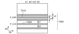
- FIG. 16C is a diagram showing the layout of the signal wiring group 7000 including wirings for transmitting the control signal P_EXP and wirings for transmitting the control signal P_CLK.
- FIG. 16C is a plan view showing a predetermined wiring layer extracted from wiring layers for a pixel circuit of one pixel.
- a wiring 7010 for the control signal P_EXP and a wiring 7020 for the control signal P_CLK are arranged extending in the first direction 30 .
- Other wirings are also arranged extending in the first direction 30, although they are not denoted by reference numerals.
- the frequency of the control signal P_EXP is higher than that of the control signal P_CLK because the control signal P_CLK transits multiple times while the control signal P_EXP is at high level. If capacitive coupling between wirings is taken into consideration, the distance between a wiring with a high frequency and the wiring adjacent to the wiring should be larger than the distance between the wiring with a low frequency and the wiring adjacent to the wiring. good. In other words, the distance between the wiring for the control signal P_CLK and the wiring adjacent to this wiring is preferably larger than the distance between the wiring for the control signal P_EXP and the wiring adjacent to this wiring.
- FIG. 16C is a layout diagram of wiring for control signals and other signal wiring.
- the distances between the wiring 7020 for the control signal P_CLK and the wiring adjacent to the wiring 7020 are s1 and s2.
- the distance between the wiring 7010 for the control signal P_EXP and the wiring adjacent to the wiring 7010 is s3 and s4. Then, s1>s3, s4 are satisfied, and s2>s3, s4 are satisfied.
- FIG. 17A shows a circuit example for clock driving. A description of the same circuits as in the fifth embodiment is omitted. A waveform shaping circuit and a counter circuit are not shown because they are the same as in FIGS. 16A to 16C.
- the power supply voltage input to the signal generating circuit 4000 can be selected between the voltage VSS (third voltage) and the voltage VQG (fourth voltage). Switching between the voltage VSS (third voltage) and the voltage VQG (fourth voltage) is performed by a control signal R_VQSEL. This switch R_VQSEL makes it possible to make the low-level voltage of the control signal QG variable.
- the pulse diagram of FIG. 17B is, for example, a part of the pulse diagram of FIG. 16B, in which the control signal P_EXP is at high level.
- the signal generating circuit 4000 is connected to the voltage VSS (third voltage). Since the control signal P_EXP is at high level, when the control signal P_CLK is at low level, the control signal QG is at high level and the PMOS transistor, which is the quench element 3010, is turned off.
- the voltage when the control signal QG is at high level is VDD (second voltage).
- control signal P_CLK when the control signal P_CLK is at a high level, the control signal P_EXP is at a high level, so the control signal QG is at a low level and the PMOS transistor as the quench element 3010 is turned on.
- the voltage when the control signal QG is at low level is VSS (third voltage).
- control signal R_VQSEL transitions from low level to high level.
- the voltage when the control signal QG is high level is VDD (second voltage) as before, but the voltage when the control signal QG is low level is VQG (fourth voltage).
- the resistance value of the quench element 3010 changes. Specifically, the resistance value of the quench element 3010 when VSS (third voltage) is applied to the gate is lower than the resistance value of the quench element 3010 when VQG (fourth voltage) is applied to the gate. Therefore, the recharge time when set to VSS (third voltage) is shorter than the recharge time when set to VQG (fourth voltage). For example, returning to FIG. 16B, recharging of Vcath is completed at the timing when QG returns from low level to high level.
- VSS third voltage
- the resistance of the quenching element 3010 will be low and the recharge time will be short. Therefore, recharging is completed before QG returns from low level to high level. Then, when a photon is incident at this timing, avalanche multiplication occurs. Furthermore, recharging is completed again until QG returns from low level to high level, and a second avalanche multiplication can occur due to a second incidence of photons. That is, in such a case, two avalanche multiplications occur before QG returns from low level to high level. That is, two or more avalanche multiplications occur for one pulse of the control signal P_CLK, resulting in unnecessary power consumption. Such a phenomenon can occur especially at high illuminance. By making the recharge time variable in this way, power consumption can be averaged in a predetermined exposure period, and as a result, there is the advantage that power consumption can be suppressed.
- the voltage VSS (third voltage) and the voltage VQG (fourth voltage) are switched during one exposure period.
- the voltage VSS (third voltage) may be used during the first exposure period
- the voltage VQG (fourth voltage) may be used during the second exposure period different from the first exposure period.
- light detection may be performed only with the voltage VSS (third voltage), or light detection may be performed only with the voltage VQG (fourth voltage).
- FIG. 17C is a wiring layout diagram for supplying the voltage VQG in the region where the pixel circuit for one pixel is provided.
- the voltage VQG is the voltage that determines the recharge time. Therefore, in order to reduce the influence from other signal wirings, it is preferable to adopt a wiring layout with low resistance. Specifically, in plan view, it is conceivable to arrange wiring in a two-dimensional direction or to increase the wiring width.
- the APD sensor including the SPAD has a large number of circuits forming a pixel circuit provided for each pixel. For this reason, there are many power supply wirings to each circuit and many input/output wirings to each circuit, and the wiring density between circuits increases. As the wiring density increases, the wiring that is desired to have a low resistance is separated in only one wiring layer, making it difficult to arrange the wiring in a two-dimensional manner. Further, as the wiring density increases, it becomes difficult to secure the space necessary for increasing the wiring width.
- the wiring 8010 of the voltage VQG (fourth voltage) is extended in the second direction 40 in the first wiring layer (M1).
- the wiring 8010 is arranged so as to reach both ends of a region where a pixel circuit for one pixel is provided.
- the wiring 8020 of the voltage VQG (fourth voltage) is extended in the first direction 30 in the second wiring layer (M2).
- Wiring 8020 is also arranged to reach both ends of the region.
- the wiring 8010 and the wiring 8020 are electrically connected by a via wiring 8030 .
- the power supply wiring can be arranged two-dimensionally, and by reducing the influence from other wirings, a stable recharge operation can be performed.
- the ratio of the area occupied by the wiring that supplies the voltage VQG (fourth voltage) is, for example, 1 ⁇ 5 or more.
- the wiring for supplying the voltage VQG (fourth voltage) is provided in the first wiring layer (M1) and the second wiring layer (M2), but the wiring may be provided in another wiring layer.
- a combination of the first wiring layer (M1) to the third wiring layer (M3) achieves a two-dimensional arrangement of wiring for the voltages VSS and VDD.
- the combination of the fourth wiring layer (M4) and the fifth wiring layer (M5) may achieve two-dimensional arrangement of the wiring of the voltage VQG.
- FIG. 18 is a modification of the cross-sectional view of the photoelectric conversion device according to the multiple embodiments described above. Since the same reference numerals are given to the parts that are common to the parts explained using FIG. 6, the explanation will be omitted. The same applies to the following modified examples.
- the wiring layer of the wiring structure 303 includes a first pad electrode 352 and a second pad electrode 354.
- the wiring layer of wiring structure 403, eg, the fifth wiring layer includes first pad electrode 352 and second pad electrode 354.
- FIG. The depth of the first pad opening 353 and the second pad opening 355 is deeper than the depth of the first pad opening 353 and the second pad opening 355 shown in FIG.
- the depth means, for example, the distance from the back surface of the semiconductor layer 302 .
- the first pad electrode 352 and the second pad electrode 354 may be positioned between the fifth surface P5 and the fourth surface P4, for example, between the fifth surface P5 and the third surface P3. do.
- the back surface of the semiconductor layer 302 is, for example, the interface with the pinning layer 341 .
- a first pad opening 353 and a second pad opening 355 extend through the bonding surface and from the semiconductor layer 302 .
- the light conversion device 100 according to the embodiment of the present invention can also have such a configuration.
- the wiring layer includes the first pad electrode 352 and the second pad electrode 354 has been described here, the pad electrodes may be formed separately from the wiring layer.
- the wiring layer of the wiring structure 303 includes the second pad electrode 354.
- a wiring layer of wiring structure 403 eg, the fifth wiring layer, includes second pad electrode 354 . That is, the second pad electrode 354 may be positioned between the fifth surface P5 and the fourth surface P4, for example, between the fifth surface P5 and the third surface P3.
- the second pad electrode 352 may be positioned between the second surface P2 and the fifth surface P5, for example, between the first surface P1 and the fifth surface P1.
- the wiring layer of the wiring structure 403 may include the first pad electrode 352 and the wiring layer of the wiring structure 303 may include the second pad electrode 354 .
- the photoelectric conversion device 100 according to this embodiment can also have such a configuration.
- the wiring layer includes the first pad electrode 352 and the second pad electrode 354 has been described here, the pad electrodes may be formed separately from the wiring layer.
- FIG. 20 shows a modification of the photoelectric conversion device 100. As shown in FIG. FIG. 20 corresponds to the cross-sectional view shown in FIG. In this modification, the structures of the first pad electrode 352 and the second pad electrode 354 are changed from the structure described with reference to FIG.
- the wiring structure 303 includes first to third wiring layers M1 to M3 and a junction 385.
- the wiring structure 403 includes first to fifth wiring layers M 1 to M 5 and junctions 395 .
- Each wiring layer is a so-called copper wiring.
- the first wiring layer includes a conductor pattern whose main component is copper.
- the conductor pattern of the first wiring layer has a single damascene structure.
- a contact is provided for electrical connection between the first wiring layer and the semiconductor layer 302 .
- a contact is a conductor pattern whose main component is tungsten.
- the second and third wiring layers include conductor patterns containing copper as a main component.
- the conductor patterns of the second and third wiring layers have a dual damascene structure and include portions functioning as wiring and portions functioning as vias.
- the fourth and subsequent wiring layers are the same as the second and third wiring layers.
- the first pad electrode 352 and the second pad electrode 354 are conductor patterns whose main component is aluminum.
- the first pad electrode 352 and the second pad electrode 354 are provided over the second and third wiring layers of the wiring structure 303 .
- it includes a portion functioning as a via connecting the first wiring layer and the second wiring layer to a portion functioning as the wiring of the third wiring layer.
- the first pad electrode 352 and the second pad electrode 354 are located, for example, between the second surface P1 and the fifth surface P5.
- the first pad electrode 352 and the second pad electrode 354 can be provided between the second surface P2 and the fourth surface P4, and can also be provided between the second surface P2 and the fifth surface P5.
- the first pad electrode 352 and the second pad electrode 354 have a first surface and a second surface opposite to the first surface. The first surface is partially exposed through an opening in the semiconductor layer.
- the exposed portions of the first pad electrode 352 and the second pad electrode 354 can function as connecting portions with external terminals, ie, so-called pad portions.
- the first pad electrode 352 and the second pad electrode 354 are connected to a plurality of copper-based conductors on their second surfaces.
- the first pad electrode 352 and the second pad electrode 354 may have electrical connection portions in the unexposed portions on the first surface side.
- the first pad electrode 352 and the second pad electrode 354 may have vias made of a conductor containing aluminum as a main component. may be electrically connected to a conductor that Also, the first pad electrode 352 and the second pad electrode 354 may be connected to the first wiring layer of the wiring structure 303 on the first surface by a conductor mainly composed of tungsten.
- the first pad electrode 352 and the second pad electrode 354 can be formed, for example, by the following procedure. After forming up to the insulator covering the third wiring layer, a part of the insulator is removed, and a film containing aluminum as a main component to be the first pad electrode 352 and the second pad electrode 354 is formed and patterned. can be formed by By forming the first pad electrode 352 and the second pad electrode 354 after forming the copper wiring, the first pad electrode 352 having a large film thickness while maintaining the flatness of the fine copper wiring. A second pad electrode 354 may be formed.
- first pad electrode 352 and the second pad electrode 354 are included in the wiring structure 303 in this modification, they may be included in the wiring structure 403 .
- the position where the pad electrode is provided may be any of the wiring structures 303 and 403, and is not limited.
- the material and structure of each wiring layer of the wiring structures 303 and 403 are not limited to those illustrated, and for example, an additional conductor layer may be provided between the wiring layer 1 and the semiconductor layer.
- the contact may have a stack contact structure in which two layers are laminated.
- FIG. 21 shows a modification of the photoelectric conversion device 100.
- FIG. FIG. 21 is a cross-sectional view enlarging the vicinity of the pad electrode 354 in the cross-sectional view shown in FIG.
- the structure of the second pad electrode 354 is mainly changed from the structure of the first embodiment.
- the wiring structure 303 includes first and second wiring layers M1 and M2 and a junction 385 .
- the wiring structure 403 includes first to fourth wiring layers M 1 to M 4 and junctions 395 .
- Each wiring layer is a so-called copper wiring.
- the first wiring layer includes a conductor pattern whose main component is copper.
- the conductor pattern of the wiring layer 1 has a single damascene structure.
- a contact is provided for electrical connection between the first wiring layer and the semiconductor layer 302 .
- a contact is a conductor pattern whose main component is tungsten.
- Other wiring layers also include conductor patterns mainly composed of copper, have a dual damascene structure, and include portions that function as wiring and portions that function as vias.
- the second pad electrode 354 is a conductor pattern whose main component is aluminum.
- the second pad electrode 354 is arranged in the opening of the semiconductor layer 302 instead of the wiring structure.
- the second pad electrode 354 has exposed surfaces on the second surface P2 and the first surface P1, but the exposed surface of the pad electrode is positioned on the second surface P2. good too.
- An opening 353 is formed in the semiconductor layer 302 such that a portion of the first wiring layer of the wiring structure 303 is exposed.
- An insulator 29 - 101 is formed to cover the second surface P 2 of the semiconductor layer 302 and the first pad opening 353 .
- An opening that becomes a via for the second pad electrode 354 is formed in the insulator 29-101.
- an opening 29-105 is formed through which the second pad electrode 354 is exposed. This configuration can be formed in such a manner.
- the through electrodes 29-104 may be provided from the second surface P2 side.
- the through electrode 29-104 is made of a conductor whose main component is copper, and may have a barrier metal between the semiconductor layer 302 and the conductor.
- a conductor 29-103 is arranged on the through electrode 29-104.
- the conductor 29-103 may be provided in common with other through electrodes, and may have a function of reducing diffusion of the conductor of the through electrodes 29-104.
- the first pad electrode 352 (not shown) can have the same configuration as the second pad electrode 354.
- the material and structure of each wiring layer of the wiring structures 303 and 403 are not limited to those illustrated, and for example, an additional conductor layer may be provided between the wiring layer 1 and the semiconductor layer.
- the contact may have a stack contact structure in which two layers are laminated.
- first pad electrode 352 and the second pad electrode 354 are positioned between the second surface P2 and the fourth surface P4, they may be positioned above the second surface P2.
- first pad opening 353 and the second pad opening 355 may be provided in the second substrate 12 .
- through electrodes may be formed in the openings.
- An electrical connection portion between the through electrode and an external device can be provided on the fourth surface P4.
- the pad electrodes which are electrical connections with an external device, may be provided on both the fourth surface P4 side of the second substrate 12 and the second surface P2 side of the first substrate 301 .
- FIG. 22 is a block diagram showing the configuration of a photoelectric conversion system 11200 according to this embodiment.
- a photoelectric conversion system 11200 of this embodiment includes a photoelectric conversion device 11204 .
- any of the photoelectric conversion devices described in the above embodiments can be applied to the photoelectric conversion device 11204 .
- the photoelectric conversion system 11200 can be used, for example, as an imaging system. Specific examples of imaging systems include digital still cameras, digital camcorders, surveillance cameras, and the like.
- FIG. 22 shows an example of a digital still camera as the photoelectric conversion system 11200 .
- a photoelectric conversion system 11200 shown in FIG. 22 has a photoelectric conversion device 11204 and a lens 11202 that forms an optical image of a subject on the photoelectric conversion device 11204 . It also has an aperture 11203 for varying the amount of light passing through the lens 11202 and a barrier 11201 for protecting the lens 11202 .
- a lens 11202 and a diaphragm 11203 are an optical system for condensing light onto the photoelectric conversion device 11204 .
- the photoelectric conversion system 11200 has a signal processing unit 11205 that processes the output signal output from the photoelectric conversion device 11204 .
- the signal processing unit 11205 performs a signal processing operation of performing various corrections and compressions on an input signal and outputting the signal as necessary.
- the photoelectric conversion system 11200 further has a buffer memory section 11206 for temporarily storing image data, and an external interface section (external I/F section) 11209 for communicating with an external computer or the like.
- the photoelectric conversion system 11200 includes a recording medium 11211 such as a semiconductor memory for recording or reading image data, and a recording medium control interface section (recording medium control I/F section) for recording or reading the recording medium 11211. 11210.
- the recording medium 11211 may be built in the photoelectric conversion system 11200 or may be detachable. Communication from the recording medium control I/F unit 11210 to the recording medium 11211 and communication from the external I/F unit 11209 may be performed wirelessly.
- the photoelectric conversion system 11200 has an overall control/calculation unit 11208 that performs various calculations and controls the entire digital still camera, and a timing generation unit 11207 that outputs various timing signals to the photoelectric conversion device 11204 and the signal processing unit 11205 .
- a timing signal or the like may be input from the outside, and the photoelectric conversion system 11200 may include at least a photoelectric conversion device 11204 and a signal processing unit 11205 that processes an output signal output from the photoelectric conversion device 11204. good.
- the overall control/arithmetic unit 11208 and the timing generation unit 11207 may be configured to implement some or all of the control functions of the photoelectric conversion device 11204 .
- the photoelectric conversion device 11204 outputs the image signal to the signal processing unit 11205 .
- a signal processing unit 11205 performs predetermined signal processing on the image signal output from the photoelectric conversion device 11204 and outputs image data. Also, the signal processing unit 11205 generates an image using the image signal. Also, the signal processing unit 11205 may perform ranging calculation on the signal output from the photoelectric conversion device 11204 .
- the signal processing unit 11205 and the timing generation unit 11207 may be mounted on the photoelectric conversion device. That is, the signal processing unit 11205 and the timing generation unit 11207 may be provided on the substrate on which the pixels are arranged, or may be provided on another substrate.
- FIG. 23 is a block diagram showing a configuration example of a distance image sensor, which is an electronic device using the photoelectric conversion device described in the above embodiments.
- the distance image sensor 12401 is configured with an optical system 12407, a photoelectric conversion device 12408, an image processing circuit 12404, a monitor 12405, and a memory 12406.
- the distance image sensor 12401 receives the light (modulated light or pulsed light) projected from the light source device 12409 toward the subject and reflected by the surface of the subject, thereby producing a distance image corresponding to the distance to the subject. can be obtained.
- the optical system 12407 includes one or more lenses, guides image light (incident light) from a subject to the photoelectric conversion device 12408, and forms an image on the light receiving surface (sensor portion) of the photoelectric conversion device 12408.
- the photoelectric conversion device of each embodiment described above is applied as the photoelectric conversion device 12408 , and a distance signal indicating the distance obtained from the received light signal output from the photoelectric conversion device 12408 is supplied to the image processing circuit 12404 .
- the image processing circuit 12404 performs image processing to construct a distance image based on the distance signal supplied from the photoelectric conversion device 12408 .
- a distance image (image data) obtained by the image processing is supplied to the monitor 12405 to be displayed, or supplied to the memory 406 to be stored (recorded).
- the range image sensor 12401 configured in this way, by applying the above-described photoelectric conversion device, it is possible to obtain, for example, a more accurate range image as the characteristics of the pixels are improved.
- the technology (the present technology) according to the present disclosure can be applied to various products.
- the technology according to the present disclosure may be applied to an endoscopic surgery system.
- FIG. 24 is a diagram showing an example of a schematic configuration of an endoscopic surgery system to which the technology according to the present disclosure (this technology) can be applied.
- FIG. 24 shows how an operator (physician) 13131 is performing surgery on a patient 13132 on a patient bed 13133 using an endoscopic surgery system 13003 .
- the endoscopic surgery system 13003 is composed of an endoscope 13100, a surgical tool 13110, and a cart 13134 on which various devices for endoscopic surgery are mounted.
- An endoscope 13100 is composed of a lens barrel 13101 having a predetermined length from its distal end inserted into the body cavity of a patient 13132 and a camera head 13102 connected to the proximal end of the lens barrel 13101 .
- an endoscope 13100 configured as a so-called rigid scope having a rigid lens barrel 13101 is illustrated, but the endoscope 13100 may be configured as a so-called flexible scope having a flexible lens barrel. good.
- the tip of the lens barrel 13101 is provided with an opening into which the objective lens is fitted.
- a light source device 13203 is connected to the endoscope 13100 , and light generated by the light source device 13203 is guided to the tip of the lens barrel 13101 by a light guide extending inside the lens barrel 13101 . In addition, this light is irradiated toward an observation target inside the body cavity of the patient 13132 through the objective lens.
- the endoscope 13100 may be a straight scope, a perspective scope, or a side scope.
- An optical system and a photoelectric conversion device are provided inside the camera head 13102, and the reflected light (observation light) from the observation target is focused on the photoelectric conversion device by the optical system.
- the photoelectric conversion device photoelectrically converts the observation light to generate an electrical signal corresponding to the observation light, that is, an image signal corresponding to the observation image.
- the photoelectric conversion device the photoelectric conversion device described in each of the above embodiments can be used.
- the image signal is transmitted to a camera control unit (CCU: Camera Control Unit) 13135 as RAW data.
- CCU Camera Control Unit
- the CCU 13135 is composed of a CPU (Central Processing Unit), a GPU (Graphics Processing Unit), etc., and controls the operations of the endoscope 13100 and the display device 13136 in an integrated manner. Further, the CCU 13135 receives an image signal from the camera head 13102 and performs various image processing such as development processing (demosaicing) for displaying an image based on the image signal.
- image processing such as development processing (demosaicing) for displaying an image based on the image signal.
- the display device 13136 displays an image based on the image signal subjected to image processing by the CCU 13135 under the control of the CCU 13135 .
- the light source device 13203 is composed of, for example, a light source such as an LED (Light Emitting Diode), and supplies the endoscope 13100 with irradiation light for photographing a surgical site or the like.
- a light source such as an LED (Light Emitting Diode)
- LED Light Emitting Diode
- the input device 13137 is an input interface for the endoscopic surgery system 13003.
- the user can input various information and instructions to the endoscopic surgery system 13003 via the input device 13137 .
- the treatment instrument control device 13138 controls driving of the energy treatment instrument 13112 for tissue cauterization, incision, or blood vessel sealing.
- the light source device 13203 that supplies irradiation light to the endoscope 13100 for photographing the surgical site can be composed of, for example, a white light source composed of an LED, a laser light source, or a combination thereof.
- a white light source is configured by combining RGB laser light sources, the output intensity and output timing of each color (each wavelength) can be controlled with high accuracy. It can be carried out.
- the object to be observed is irradiated with laser light from each of the RGB laser light sources in a time division manner, and by controlling the drive of the imaging element of the camera head 13102 in synchronization with the irradiation timing, each of RGB can be handled. It is also possible to pick up images by time division. According to this method, a color image can be obtained without providing a color filter in the imaging element.
- the driving of the light source device 13203 may be controlled so as to change the intensity of the output light every predetermined time.
- the drive of the imaging device of the camera head 13102 in synchronism with the timing of the change in the intensity of the light to obtain images in a time-division manner and synthesizing the images, a high dynamic A range of images can be generated.
- the light source device 13203 may be configured to be capable of supplying light in a predetermined wavelength band corresponding to special light observation.
- Special light observation for example, utilizes the wavelength dependence of light absorption in body tissues. Specifically, a predetermined tissue such as a blood vessel on the surface of the mucous membrane is imaged with high contrast by irradiating light with a narrower band than the irradiation light (that is, white light) used during normal observation.
- irradiation light that is, white light
- fluorescence observation may be performed in which an image is obtained from fluorescence generated by irradiation with excitation light.
- body tissue is irradiated with excitation light and fluorescence from the body tissue is observed, or a reagent such as indocyanine green (ICG) is locally injected into the body tissue and the fluorescence wavelength of the reagent is observed in the body tissue. It is possible to obtain a fluorescent image by irradiating excitation light corresponding to .
- the light source device 13203 can be configured to supply narrowband light and/or excitation light corresponding to such special light observation.
- FIGS. 25A, 25B, 26A, and 26B are schematic diagrams showing configuration examples of a photoelectric conversion system and a moving object according to this embodiment.
- an example of an in-vehicle camera is shown as a photoelectric conversion system.
- FIGs. 25A and 25B show an example of a vehicle system and a photoelectric conversion system mounted therein for imaging.
- a photoelectric conversion system 14301 includes a photoelectric conversion device 14302 , an image preprocessing unit 14315 , an integrated circuit 14303 and an optical system 14314 .
- the optical system 14314 forms an optical image of a subject on the photoelectric conversion device 14302 .
- the photoelectric conversion device 14302 converts the optical image of the object formed by the optical system 14314 into an electrical signal.
- the photoelectric conversion device 14302 is the photoelectric conversion device according to any one of the embodiments described above.
- An image preprocessing unit 14315 performs predetermined signal processing on the signal output from the photoelectric conversion device 14302 .
- the functions of the image preprocessing unit 14315 may be incorporated within the photoelectric conversion device 14302 .
- the photoelectric conversion system 14301 is provided with at least two sets of an optical system 14314, a photoelectric conversion device 14302, and an image preprocessing unit 14315, and the output from each set of image preprocessing units 14315 is input to an integrated circuit 14303. It's like
- the integrated circuit 14303 is an integrated circuit for use in imaging systems, and includes an image processing unit 14304 including a memory 14305, an optical distance measurement unit 14306, a distance calculation unit 14307, an object recognition unit 14308, and an abnormality detection unit 14309.
- An image processing unit 14304 performs image processing such as development processing and defect correction on the output signal of the image preprocessing unit 14315 .
- the memory 14305 temporarily stores captured images and stores defect positions of captured pixels.
- An optical distance measuring unit 14306 performs focusing of a subject and distance measurement.
- a ranging calculation unit 14307 calculates ranging information from a plurality of image data acquired by a plurality of photoelectric conversion devices 14302 .
- the object recognition unit 14308 recognizes subjects such as cars, roads, signs, and people.
- the abnormality detection unit 14309 detects an abnormality in the photoelectric conversion device 14302, the abnormality detection unit 14309 notifies the main control unit 14313 of the abnormality.
- the integrated circuit 14303 may be realized by specially designed hardware, software modules, or a combination thereof. Also, it may be realized by FPGA (Field Programmable Gate Array), ASIC (Application Specific Integrated Circuit), etc., or by a combination thereof.
- FPGA Field Programmable Gate Array
- ASIC Application Specific Integrated Circuit
- the main control unit 14313 integrates and controls the operations of the photoelectric conversion system 14301, the vehicle sensor 14310, the control unit 14320, and the like. There is also a method in which the photoelectric conversion system 14301, the vehicle sensor 14310, and the control unit 14320 have individual communication interfaces without the main control unit 14313, and each of them transmits and receives control signals via a communication network (for example, CAN standard).
- a communication network for example, CAN standard
- the integrated circuit 14303 has a function of receiving a control signal from the main control unit 14313 or transmitting a control signal and setting values to the photoelectric conversion device 14302 by its own control unit.
- the photoelectric conversion system 14301 is connected to a vehicle sensor 14310, and can detect the running state of the own vehicle such as vehicle speed, yaw rate, and steering angle, the environment outside the own vehicle, and the state of other vehicles and obstacles.
- the vehicle sensor 14310 also serves as distance information acquisition means for acquiring distance information to an object.
- the photoelectric conversion system 14301 is also connected to a driving support control unit 1311 that performs various driving support functions such as automatic steering, automatic cruise, and anti-collision functions.
- the collision determination function based on the detection results of the photoelectric conversion system 14301 and the vehicle sensor 14310, it is possible to estimate a collision with another vehicle/obstacle and determine whether or not there is a collision. As a result, avoidance control when a collision is presumed and safety device activation at the time of collision are performed.
- the photoelectric conversion system 14301 is also connected to an alarm device 14312 that issues an alarm to the driver based on the judgment result of the collision judgment section. For example, when the collision possibility is high as a result of the judgment by the collision judging section, the main control section 14313 controls the vehicle to avoid collision and reduce damage by applying the brake, releasing the accelerator, or suppressing the engine output. conduct.
- the alarm device 14312 warns the user by sounding an alarm such as sound, displaying alarm information on a display unit screen of a car navigation system or a meter panel, or vibrating a seat belt or steering wheel.
- the photoelectric conversion system 14301 photographs the surroundings of the vehicle, for example, the front or rear.
- FIG. 25B shows an arrangement example of the photoelectric conversion system 14301 when the photoelectric conversion system 14301 captures an image in front of the vehicle.
- the two photoelectric conversion devices 14302 are arranged in front of the vehicle 14300 .
- the axis of symmetry is the center line of the vehicle 14300 with respect to the forward/retreat direction or the outer shape (for example, the width of the vehicle). If the two photoelectric conversion devices 1302 are arranged symmetrically with respect to this axis of symmetry, it is preferable to obtain information on the distance between the vehicle 14300 and the object to be photographed and to determine the possibility of collision.
- the photoelectric conversion device 14302 is preferably arranged so as not to block the driver's field of view when the driver visually recognizes the situation outside the vehicle 14300 from the driver's seat. It is preferable that the warning device 14312 be arranged so as to be easily visible to the driver.
- the control that does not collide with another vehicle has been described, but it is also applicable to control that automatically drives following another vehicle, control that automatically drives so as not to stray from the lane, and the like.
- the photoelectric conversion system 14301 can be applied not only to a vehicle such as a vehicle, but also to a moving object (moving device) such as a ship, an aircraft, or an industrial robot.
- the present invention can be applied not only to mobile objects but also to devices that widely use object recognition, such as intelligent transportation systems (ITS).
- ITS intelligent transportation systems
- the photoelectric conversion device of the present invention may further have a configuration capable of acquiring various information such as distance information.
- FIG. 11 illustrate eyeglasses 16600 (smart glasses) according to one application.
- Glasses 16600 have a photoelectric conversion device 16602 .
- the photoelectric conversion device 16602 is the photoelectric conversion device described in each of the above embodiments.
- a display device including a light emitting device such as an OLED or an LED may be provided on the rear surface side of the lens 16601 .
- One or more photoelectric conversion devices 16602 may be provided. Further, a plurality of types of photoelectric conversion devices may be used in combination.
- the arrangement position of the photoelectric conversion device 16602 is not limited to that shown in FIG. 26A.
- the spectacles 16600 further include a control device 16603.
- the control device 16603 functions as a power source that supplies power to the photoelectric conversion device 16602 and the display device.
- the control device 16603 controls operations of the photoelectric conversion device 16602 and the display device.
- the lens 16601 is formed with an optical system for condensing light onto the photoelectric conversion device 16602 .
- FIG. 26B illustrates glasses 16610 (smart glasses) according to one application.
- the glasses 16610 have a control device 16612, and the control device 16612 is equipped with a photoelectric conversion device corresponding to the photoelectric conversion device 16602 and a display device.
- a photoelectric conversion device in the control device 16612 and an optical system for projecting light emitted from the display device are formed on the lens 16611 , and an image is projected onto the lens 16611 .
- the control device 16612 functions as a power source that supplies power to the photoelectric conversion device and the display device, and controls the operation of the photoelectric conversion device and the display device.
- the control device may have a line-of-sight detection unit that detects the line of sight of the wearer.
- Infrared rays may be used for line-of-sight detection.
- the infrared light emitting unit emits infrared light to the eyeballs of the user who is gazing at the display image.
- a captured image of the eyeball is obtained by detecting reflected light of the emitted infrared light from the eyeball by an imaging unit having a light receiving element.
- the user's line of sight to the display image is detected from the captured image of the eyeball obtained by capturing infrared light.
- Any known method can be applied to line-of-sight detection using captured images of eyeballs.
- line-of-sight detection processing is performed based on the pupillary corneal reflection method.
- the user's line of sight is detected by calculating a line-of-sight vector representing the orientation (rotational angle) of the eyeball based on the pupil image and the Purkinje image included in the captured image of the eyeball using the pupillary corneal reflection method. be.
- the display device of the present embodiment may have a photoelectric conversion device having a light receiving element, and may control the display image of the display device based on the user's line-of-sight information from the photoelectric conversion device.
- the display device determines a first visual field area that the user gazes at and a second visual field area other than the first visual field area, based on the line-of-sight information.
- the first viewing area and the second viewing area may be determined by the control device of the display device, or may be determined by an external control device.
- the display resolution of the first viewing area may be controlled to be higher than the display resolution of the second viewing area. That is, the resolution of the second viewing area may be lower than that of the first viewing area.
- the display area has a first display area and a second display area different from the first display area. may be determined.
- the first viewing area and the second viewing area may be determined by the control device of the display device, or may be determined by an external control device.
- the resolution of areas with high priority may be controlled to be higher than the resolution of areas other than areas with high priority. In other words, the resolution of areas with relatively low priority may be lowered.
- AI may be used to determine the first field of view area and areas with high priority.
- the AI is a model configured to estimate the angle of the line of sight from the eyeball image and the distance to the object ahead of the line of sight, using the image of the eyeball and the direction in which the eyeball of the image was actually viewed as training data. It can be.
- the AI program may be owned by the display device, the photoelectric conversion device, or the external device. If the external device has it, it is communicated to the display device via communication.
- display control based on visual recognition detection it can be preferably applied to smart glasses that further have a photoelectric conversion device that captures an image of the outside.
- the smart glasses can display captured external information in real time.
Abstract
The present invention addresses the technical problem of arranging wiring in a photoelectric conversion device that includes an avalanche photodiode. Provided is a photoelectric conversion device, wherein: a first substrate and a second substrate are stacked between a first semiconductor layer and a second semiconductor layer so that a first wiring structure and a second wiring structure can be provided; a plurality of wiring layers of the second wiring structure includes a wiring layer in which a first wiring that supplies power supply voltage to a plurality of pixel circuits is provided and in which an occupied area of the first wiring is the greatest among the plurality of wiring layers, and includes wiring layer groups that are provided between the second semiconductor layer and the wiring layer in which the first wiring is provided and the occupied area of the first wiring is the greatest among the plurality of wiring layers; and when viewed from above, the first wiring is configured such that both ends in a first direction of a region in which each of the plurality of pixel circuits is provided and both ends in a second direction that crosses the first direction are connected by a combination of the wiring layer groups.
Description
本発明は、光電変換装置、光電変換システム、および移動体に関する。
The present invention relates to a photoelectric conversion device, a photoelectric conversion system, and a moving body.
複数のアバランシェフォトダイオード(以下、APD:Avalanche Photo Diode)を含む画素が平面的に2次元アレイ状に配置されるように構成された画素アレイを含む光電変換装置が知られている。各画素においては、PN接合ダイオードに対して、逆バイアスの電圧を印加することで、単一光子に起因した光電荷がアバランシェ増倍を起こす。APDの動作には少なくとも2つのモードがある。逆バイアスの電圧が供給される場合において、アノードおよびカソードの電位差が降伏電圧より大きいな電位差で動作させるガイガーモードと、アノードおよびカソードの電位差が降伏電圧近傍、またはそれ以下の電圧差で動作させるリニアモードである。このうち、ガイガーモードで動作させるAPDをSPAD(Single Photon Avalanche Diode)と呼ぶ。
A photoelectric conversion device is known that includes a pixel array configured such that pixels including a plurality of avalanche photodiodes (hereinafter referred to as APDs) are arranged in a planar two-dimensional array. In each pixel, by applying a reverse bias voltage to the PN junction diode, photocharge caused by a single photon causes avalanche multiplication. There are at least two modes of APD operation. When a reverse bias voltage is supplied, the Geiger mode operates with a potential difference between the anode and cathode greater than the breakdown voltage, and the linear mode operates with a voltage difference near or below the breakdown voltage between the anode and cathode. mode. Among these, an APD operated in Geiger mode is called a SPAD (Single Photon Avalanche Diode).
特許文献1には、第1基板と第2基板を積層したSPADセンサであって、第1基板にAPDを有し、第2基板にAPDからの信号を処理する信号処理回路が設けられた構成が開示されている。また、特許文献1には、光子の入射個数をカウントするカウンタ回路が設けられている。
Patent Document 1 discloses a SPAD sensor in which a first substrate and a second substrate are laminated, the first substrate having an APD, and the second substrate having a signal processing circuit for processing signals from the APD. is disclosed. Further, in Patent Document 1, a counter circuit for counting the number of incident photons is provided.
APDセンサは、CMOSセンサと比較して、画素の回路数が多く、回路への電源配線や、回路への入出力配線が多く、配線密度が高くなる。しかしながら、特許文献1では、APDセンサで配線密度が高くなった場合に生じる課題を解決する配線の構成が提案されていない。
Compared to CMOS sensors, APD sensors have more pixel circuits, more power supply wiring to the circuits, more input/output wiring to the circuits, and higher wiring density. However, Patent Literature 1 does not propose a wiring configuration that solves the problem that occurs when the wiring density increases in the APD sensor.
そこで、本発明は、APDセンサで配線密度が高くなった場合に生じる課題を解決する配線の構成を提案することを目的とする。
Therefore, an object of the present invention is to propose a wiring configuration that solves the problems that arise when wiring density increases in APD sensors.
本発明に係る光電変換装置は、複数の光電変換部を備えた第1半導体層と、少なくとも1つの配線層を備えた第1配線構造を有する第1基板と、前記複数の光電変換部のそれぞれに対応して、それぞれ設けられた複数の画素回路を備えた第2半導体層と、複数の配線層を備えた第2配線構造を有する第2基板と、を有し、前記複数の光電変換部のそれぞれは、アバランシェフォトダイオードを有しており、前記第1半導体層と前記第2半導体層との間に、前記第1配線構造と前記第2配線構造が設けられるように、前記第1基板と前記第2基板が積層されており、前記第1配線構造または前記第2配線構造は、前記アバランシェフォトダイオードに電圧を供給するパッド電極を有し、前記第2配線構造の前記複数の配線層は、前記複数の画素回路に電源電圧を供給する第1配線が配され、かつ、前記複数の配線層の中で前記第1配線の占有面積が最も大きい配線層と、前記第1配線が配され、かつ、前記複数の配線層の中で前記第1配線の占有面積が最も大きい配線層と前記第2半導体層との間に設けられた、配線層群と、を有し、平面視において、前記第1配線は、前記配線層群の組み合わせにより、前記複数の画素回路のそれぞれが設けられている領域の第1方向の両端と、前記第1方向と交差する第2方向の両端とが接続されるように構成されていることを特徴とする。
A photoelectric conversion device according to the present invention includes: a first semiconductor layer including a plurality of photoelectric conversion units; a first substrate having a first wiring structure including at least one wiring layer; and a second substrate having a second wiring structure with a plurality of wiring layers, the plurality of photoelectric conversion units has an avalanche photodiode, and the first substrate such that the first wiring structure and the second wiring structure are provided between the first semiconductor layer and the second semiconductor layer. and the second substrate are laminated, the first wiring structure or the second wiring structure has a pad electrode for supplying a voltage to the avalanche photodiode, and the plurality of wiring layers of the second wiring structure is arranged with a first wiring for supplying a power supply voltage to the plurality of pixel circuits, and a wiring layer having the largest area occupied by the first wiring among the plurality of wiring layers; and the first wiring. and a wiring layer group provided between the wiring layer in which the first wiring occupies the largest area among the plurality of wiring layers and the second semiconductor layer, in plan view , the first wiring has both ends in a first direction of a region in which each of the plurality of pixel circuits is provided and both ends in a second direction crossing the first direction, depending on the combination of the wiring layer groups. It is characterized by being configured to be connected.
本発明によれば、APDセンサで配線密度が高くなった場合に生じる課題を解決する配線の構成を提案することができる。
According to the present invention, it is possible to propose a wiring configuration that solves the problem that occurs when the wiring density increases in the APD sensor.
以下に示す形態は、本発明の技術思想を具体化するためのものであって、本発明を限定するものではない。各図面が示す部材の大きさや位置関係は、説明を明確にするために誇張していることがある。以下の説明において、同一の構成については同一の番号を付して説明を省略することがある。
The form shown below is for embodying the technical idea of the present invention, and does not limit the present invention. The sizes and positional relationships of members shown in each drawing may be exaggerated for clarity of explanation. In the following description, the same configuration may be assigned the same number and the description thereof may be omitted.
以下に示す形態は、特にアバランシェダイオードに入射するフォトンの数を数えるSPAD(Single Photon Avalanche Diode)を備える光電変換装置に関する。光電変換装置は、少なくともアバランシェダイオードを備えていればよく、ガイガーモードだけでなく、リニアモードで動作させてもよい。
The embodiments shown below particularly relate to a photoelectric conversion device including a SPAD (Single Photon Avalanche Diode) that counts the number of photons incident on an avalanche diode. A photoelectric conversion device may include at least an avalanche diode, and may be operated in a linear mode as well as a Geiger mode.
以下の説明において、アバランシェダイオードのアノードを固定電位とし、カソード側から信号を取り出している。したがって、信号電荷と同じ導電型の電荷を多数キャリアとする第1導電型の半導体領域とはN型半導体領域であり、第2導電型の半導体領域とはP型半導体領域である。なお、アバランシェダイオードのカソードを固定電位とし、アノード側から信号を取り出す場合でも本発明は成立する。この場合は、信号電荷と同じ導電型の電荷を多数キャリアとする第1導電型の半導体領域はP型半導体領域であり、第2導電型の半導体領域とはN型半導体領域である。以下では、アバランシェダイオードの一方のノードを固定電位とする場合について説明するが、両方のノードの電位が変動してもよい。
In the following explanation, the anode of the avalanche diode is set to a fixed potential and the signal is extracted from the cathode side. Therefore, the semiconductor region of the first conductivity type in which majority carriers are the same conductivity type as the signal charges is the N-type semiconductor region, and the semiconductor region of the second conductivity type is the P-type semiconductor region. The present invention can also be applied when the cathode of the avalanche diode is set at a fixed potential and the signal is extracted from the anode side. In this case, the semiconductor region of the first conductivity type having majority carriers of the same conductivity type as the signal charge is a P-type semiconductor region, and the semiconductor region of the second conductivity type is an N-type semiconductor region. Although the case where one node of the avalanche diode is set to a fixed potential will be described below, the potentials of both nodes may fluctuate.
本明細書において、平面視とは、半導体層の光入射面に対して垂直な方向から視ることである。また、断面視とは、半導体層の光入射面と垂直な方向における面をいう。なお、微視的に見て半導体層の光入射面が粗面である場合は、巨視的に見たときの半導体層の光入射面を基準として平面視を定義する。
In this specification, "planar view" means viewing from a direction perpendicular to the light incident surface of the semiconductor layer. A cross-sectional view refers to a plane in a direction perpendicular to the light incident surface of the semiconductor layer. When the light incident surface of the semiconductor layer is microscopically rough, the plane view is defined based on the light incident surface of the semiconductor layer macroscopically.
また、本明細書において、便宜上、半導体層に最も近い配線層を第1配線層とし、半導体層から遠ざかる方向の順序で第2配線層、第3配線層等と説明することがある。しかし、特許請求の範囲においては、特許請求の範囲に記載の文言で特定されていない限り、「第1配線層」は半導体層に最も近い配線層ではないし、序数は配線層の順番を意味しない。
Also, in this specification, for the sake of convenience, the wiring layer closest to the semiconductor layer may be referred to as the first wiring layer, and the second wiring layer, the third wiring layer, etc. may be described in order in the direction away from the semiconductor layer. However, in the claims, unless specified in the claim language, the "first wiring layer" is not the wiring layer closest to the semiconductor layer, and the ordinal numbers do not imply the order of the wiring layers. .
(実施形態1)
(光電変換装置の全体ブロック図)
図1は、光電変換装置100の全体像を示す図である。第1基板11は、センサチップともいい、光電変換部を有する画素が二次元状に配列されている画素領域12が設けられている。また、画素領域12と光電変換装置100のチップ端部の間には、周辺領域13が設けられている。第2基板21は、画素回路チップともいい、光電変換部からの信号を処理する信号処理回路領域22が設けられている。第1基板11と、第2基板21が積層されることにより、光電変換装置100が構成されている。なお、不図示であるが、第3基板を第1基板と第2基板の積層体にさらに積層することも可能である。この場合、第3基板には、第2基板21から出力された信号を処理する信号処理回路を設けることが可能である。例えば、信号処理回路として、メモリに格納されているプログラムを実行することで、機械学習によって作成された学習済みモデルを用いて各種処理を実行する処理回路を設けてもよい。学習済みモデルは、ディープニューラルネットワーク(DNN)を利用した機械学習によって作成される。この信号処理回路は、画素領域から出力した信号を用いて、学習済みモデルに基づいた演算処理を実行する。演算結果には、学習済みモデルを用いた演算処理を実行することで得られた画像データや、その画像データから得られる各種情報(メタデータ)が含まれる。 (Embodiment 1)
(Overall block diagram of photoelectric conversion device)
FIG. 1 is a diagram showing an overall image of aphotoelectric conversion device 100. FIG. The first substrate 11 is also called a sensor chip, and is provided with a pixel region 12 in which pixels having photoelectric conversion units are arranged two-dimensionally. A peripheral region 13 is provided between the pixel region 12 and the chip edge of the photoelectric conversion device 100 . The second substrate 21 is also called a pixel circuit chip, and is provided with a signal processing circuit area 22 for processing signals from the photoelectric conversion section. The photoelectric conversion device 100 is configured by stacking the first substrate 11 and the second substrate 21 . Although not shown, it is also possible to further laminate a third substrate on the laminate of the first substrate and the second substrate. In this case, a signal processing circuit for processing the signal output from the second substrate 21 can be provided on the third substrate. For example, as the signal processing circuit, a processing circuit that executes various processes using a learned model created by machine learning by executing a program stored in a memory may be provided. A trained model is created by machine learning using a deep neural network (DNN). This signal processing circuit uses the signal output from the pixel area to perform arithmetic processing based on the learned model. The calculation result includes image data obtained by executing calculation processing using the trained model and various information (metadata) obtained from the image data.
(光電変換装置の全体ブロック図)
図1は、光電変換装置100の全体像を示す図である。第1基板11は、センサチップともいい、光電変換部を有する画素が二次元状に配列されている画素領域12が設けられている。また、画素領域12と光電変換装置100のチップ端部の間には、周辺領域13が設けられている。第2基板21は、画素回路チップともいい、光電変換部からの信号を処理する信号処理回路領域22が設けられている。第1基板11と、第2基板21が積層されることにより、光電変換装置100が構成されている。なお、不図示であるが、第3基板を第1基板と第2基板の積層体にさらに積層することも可能である。この場合、第3基板には、第2基板21から出力された信号を処理する信号処理回路を設けることが可能である。例えば、信号処理回路として、メモリに格納されているプログラムを実行することで、機械学習によって作成された学習済みモデルを用いて各種処理を実行する処理回路を設けてもよい。学習済みモデルは、ディープニューラルネットワーク(DNN)を利用した機械学習によって作成される。この信号処理回路は、画素領域から出力した信号を用いて、学習済みモデルに基づいた演算処理を実行する。演算結果には、学習済みモデルを用いた演算処理を実行することで得られた画像データや、その画像データから得られる各種情報(メタデータ)が含まれる。 (Embodiment 1)
(Overall block diagram of photoelectric conversion device)
FIG. 1 is a diagram showing an overall image of a
(第1基板の構成図)
図2は、第1基板11の構成図である。第1基板には、アバランシェフォトダイオード(以下、APD)を含む光電変換部102を有する画素101が二次元状に配された画素領域12が設けられている。画素領域12における画素101の配列は1次元状に配されていてもよい。光電変換部102の詳細については、後述する。 (Construction diagram of the first substrate)
FIG. 2 is a configuration diagram of thefirst substrate 11. As shown in FIG. A first substrate is provided with a pixel region 12 in which pixels 101 each having a photoelectric conversion unit 102 including an avalanche photodiode (hereinafter referred to as APD) are arranged two-dimensionally. The pixels 101 in the pixel region 12 may be arranged one-dimensionally. Details of the photoelectric conversion unit 102 will be described later.
図2は、第1基板11の構成図である。第1基板には、アバランシェフォトダイオード(以下、APD)を含む光電変換部102を有する画素101が二次元状に配された画素領域12が設けられている。画素領域12における画素101の配列は1次元状に配されていてもよい。光電変換部102の詳細については、後述する。 (Construction diagram of the first substrate)
FIG. 2 is a configuration diagram of the
画素101は、典型的には、画像を形成するための画素であるが、TOF(Time of Flight)に用いる場合には、必ずしも画像を形成しなくてもよい。すなわち、画素101は、光が到達した時刻と光量を測定するための素子であってもよい。
The pixels 101 are typically pixels for forming an image, but when used for TOF (Time of Flight), they do not necessarily form an image. That is, the pixel 101 may be an element for measuring the time and amount of light that light reaches.
(第2基板の構成図)
図3Aは、第2基板21の構成図である。第2基板21は、光電変換部102で光電変換された信号を処理する信号処理部103が複数設けられている。複数の信号処理部103は、2次元状に配された信号処理回路領域22に設けられている。信号処理部103は各画素に対応して配される画素回路でもある。信号処理部103は、カウンタやメモリなどが設けられており、メモリにはデジタル値が保持される。信号処理部103から出力される信号は、垂直走査回路110と、水平走査回路111を用いて、信号線113に伝達される。 (Construction diagram of the second substrate)
3A is a configuration diagram of thesecond substrate 21. FIG. The second substrate 21 is provided with a plurality of signal processing units 103 that process signals photoelectrically converted by the photoelectric conversion units 102 . The plurality of signal processing units 103 are provided in the signal processing circuit area 22 arranged two-dimensionally. The signal processing unit 103 is also a pixel circuit arranged corresponding to each pixel. The signal processing unit 103 is provided with a counter, a memory, and the like, and a digital value is held in the memory. A signal output from the signal processing unit 103 is transmitted to a signal line 113 using a vertical scanning circuit 110 and a horizontal scanning circuit 111 .
図3Aは、第2基板21の構成図である。第2基板21は、光電変換部102で光電変換された信号を処理する信号処理部103が複数設けられている。複数の信号処理部103は、2次元状に配された信号処理回路領域22に設けられている。信号処理部103は各画素に対応して配される画素回路でもある。信号処理部103は、カウンタやメモリなどが設けられており、メモリにはデジタル値が保持される。信号処理部103から出力される信号は、垂直走査回路110と、水平走査回路111を用いて、信号線113に伝達される。 (Construction diagram of the second substrate)
3A is a configuration diagram of the
垂直走査回路110は、制御パルス生成部115から供給された制御パルスを受け、各画素に制御パルスを供給する。垂直走査回路110にはシフトレジスタやアドレスデコーダといった論理回路が用いられる。
The vertical scanning circuit 110 receives the control pulse supplied from the control pulse generator 115 and supplies the control pulse to each pixel. A logic circuit such as a shift register or an address decoder is used for the vertical scanning circuit 110 .
水平走査回路111は、デジタル信号が保持された各画素のメモリから信号を読み出すために、各列を順次選択する制御パルスを信号処理部103に入力する。
The horizontal scanning circuit 111 inputs a control pulse for sequentially selecting each column to the signal processing unit 103 in order to read the signal from the memory of each pixel holding the digital signal.
信号線113には、選択されている列について、垂直走査回路110により選択された画素の信号処理部103から信号が出力される。
A signal is output to the signal line 113 from the signal processing unit 103 of the pixel selected by the vertical scanning circuit 110 for the selected column.
信号線113に伝達された信号は、読み出し回路112および出力回路114から外部に出力される。信号線113は上下方向に延在するように配されている。垂直走査回路110、水平走査回路111、読み出し回路112は、制御パルス生成部115からのパルスによって制御される。
The signal transmitted to the signal line 113 is output from the readout circuit 112 and the output circuit 114 to the outside. The signal line 113 is arranged to extend vertically. The vertical scanning circuit 110 , horizontal scanning circuit 111 , and readout circuit 112 are controlled by pulses from the control pulse generator 115 .
図3Bは、第2基板21の別形態である。図3Aでは、信号線が上下方向(列方向)に延在するように配されていたが、図3Bでは、信号線が左右方向(水平方向)に延在するように配されている点が異なる。このため、図3Aでは、信号処理回路領域22の下部に読み出し回路112が設けられているのに対して、図3Bでは、信号処理回路領域22の右に読み出し回路112が設けられている。
3B is another form of the second substrate 21. FIG. In FIG. 3A, the signal lines are arranged to extend in the vertical direction (column direction), but in FIG. 3B, the signal lines are arranged to extend in the horizontal direction (horizontal direction). different. For this reason, the readout circuit 112 is provided below the signal processing circuit region 22 in FIG. 3A, whereas the readout circuit 112 is provided to the right of the signal processing circuit region 22 in FIG. 3B.
図2および図3A、図3Bでは、1つの画素101に対応して1つの信号処理部103が設けられていた。しかし、信号処理部103は、例えば、複数の画素101によって1つの信号処理部103が共有され、順次信号処理が行われてもよい。これにより、信号処理回路領域22の省スペース化を図ることができる。
In FIGS. 2, 3A, and 3B, one signal processing unit 103 is provided for one pixel 101. FIG. However, for example, one signal processing unit 103 may be shared by a plurality of pixels 101 and signal processing may be performed sequentially. Thereby, space saving of the signal processing circuit area 22 can be achieved.
(光電変換装置の機能ブロック図)
図4は、図2および図3A、図3Bで説明したブロック図をより詳細に説明する図である。 (Functional block diagram of photoelectric conversion device)
FIG. 4 is a diagram illustrating in more detail the block diagrams described in FIGS. 2 and 3A and 3B.
図4は、図2および図3A、図3Bで説明したブロック図をより詳細に説明する図である。 (Functional block diagram of photoelectric conversion device)
FIG. 4 is a diagram illustrating in more detail the block diagrams described in FIGS. 2 and 3A and 3B.
図4において、APD3100は、第1基板11に設けられており、その他の部材は、第2基板21に設けられていることを示している。
4 shows that the APD 3100 is provided on the first substrate 11 and the other members are provided on the second substrate 21. FIG.
APD3100は、光が入射すると、光電変換により電荷対が生成される。APD3100のアノードには、電圧VPDL(第1電圧)が供給される。また、APD3100のカソードには、アノードに供給される電圧VPDLよりも高い電圧VDD(第2電圧)が供給される。
When light is incident on the APD 3100, charge pairs are generated by photoelectric conversion. A voltage VPDL (first voltage) is supplied to the anode of the APD 3100 . Also, the cathode of the APD 3100 is supplied with a voltage VDD (second voltage) higher than the voltage VPDL supplied to the anode.
アノードとカソードには、APD3100がアバランシェ増倍動作をするような逆バイアス電圧が供給される。このような電圧を供給した状態とすることで、入射光によって生じた電荷がアバランシェ増倍を起こし、アバランシェ電流が発生する。
A reverse bias voltage is supplied to the anode and cathode so that the APD 3100 performs an avalanche multiplication operation. By supplying such a voltage, charges generated by the incident light undergo avalanche multiplication, generating an avalanche current.
逆バイアスの電圧が供給される場合において、アノードおよびカソードの電位差が降伏電圧より大きい電位差で動作させるモードをガイガーモードという。また、アノードおよびカソードの電位差が降伏電圧近傍、もしくはそれ以下の電圧差で動作させるモードをリニアモードという。このうち、ガイガーモードで動作させるAPDをSPADと呼ぶ。例えば、電圧VPDL(第1電圧)は、-30V、電圧VDD(第2電圧)は、1Vである。この場合、例えば、電圧VSS(第3電圧)である0Vと電圧VPDL(第1電圧)の電位差は、電圧VSS(第3電圧)と電圧VH(第2電圧)の電位差よりも大きい。そのため、電圧VPDL(第1電圧)を高電圧と表現することもある。
When a reverse bias voltage is supplied, the Geiger mode is a mode in which the potential difference between the anode and cathode is greater than the breakdown voltage. A linear mode is a mode in which the potential difference between the anode and cathode is close to or less than the breakdown voltage. Among them, an APD operated in the Geiger mode is called a SPAD. For example, the voltage VPDL (first voltage) is -30V, and the voltage VDD (second voltage) is 1V. In this case, for example, the potential difference between 0 V, which is the voltage VSS (third voltage), and the voltage VPDL (first voltage) is greater than the potential difference between the voltage VSS (third voltage) and the voltage VH (second voltage). Therefore, the voltage VPDL (first voltage) is sometimes expressed as a high voltage.
クエンチ素子3010は、電圧VDDを供給する電源とAPD3100に接続される。クエンチ素子3010は、APD3100で生じたアバランシェ電流の変化を電圧信号に置き換える機能を有する。クエンチ素子3010は、アバランシェ増倍による信号増倍時に負荷回路(クエンチ素子)として機能し、APD3100に供給する電圧を抑制して、アバランシェ増倍を抑制する働きを持つ(クエンチ動作)。
The quenching element 3010 is connected to the power supply supplying the voltage VDD and the APD 3100 . The quench element 3010 has the function of converting the change in avalanche current generated by the APD 3100 into a voltage signal. The quench element 3010 functions as a load circuit (quench element) during signal multiplication by avalanche multiplication, suppresses the voltage supplied to the APD 3100, and has a function of suppressing avalanche multiplication (quench operation).
画素回路3000は、クエンチ素子3010の他に、波形整形回路3020、処理回路3030、カウンタ回路3040、出力回路3050を有する。
The pixel circuit 3000 has a waveform shaping circuit 3020 , a processing circuit 3030 , a counter circuit 3040 and an output circuit 3050 in addition to the quenching element 3010 .
波形整形回路3020は、光子検出時に得られるAPD3100のカソードの電位変化を整形して、パルス信号を出力する。波形整形回路3020としては、例えば、インバータ回路が用いられる。波形整形回路212は、1つのインバータを用いてもよいし、複数のインバータを直列接続した回路を用いてもよいし、波形整形効果があるその他の回路を用いてもよい。
A waveform shaping circuit 3020 shapes the potential change of the cathode of the APD 3100 obtained during photon detection, and outputs a pulse signal. As the waveform shaping circuit 3020, for example, an inverter circuit is used. The waveform shaping circuit 212 may use one inverter, a circuit in which a plurality of inverters are connected in series, or other circuits having waveform shaping effects.
処理回路3030は、任意の信号処理を行う回路である。例えば、処理回路3030は、波形整形回路3020から出力する信号をカウンタ回路3040に入力するか否かを選択する回路である。より具体的には、露光期間では、処理回路3030は、波形整形回路3020から出力されたパルス信号をカウンタ回路3040に入力するように構成される。他方、非露光期間では、処理回路3030は、波形整形回路3020からパルス信号が出力したとしても、カウンタ回路3040には入力しないように構成される。ところで、露光期間と非露光期間を設定するためには、後述するように、クエンチ素子3010の制御により、これらの期間の切り替えが可能である。上記した処理回路3030を設ければ、クエンチ素子3010の制御によらず、露光期間と非露光期間の制御が可能である。
The processing circuit 3030 is a circuit that performs arbitrary signal processing. For example, the processing circuit 3030 is a circuit that selects whether or not to input the signal output from the waveform shaping circuit 3020 to the counter circuit 3040 . More specifically, during the exposure period, the processing circuit 3030 is configured to input the pulse signal output from the waveform shaping circuit 3020 to the counter circuit 3040 . On the other hand, during the non-exposure period, the processing circuit 3030 is configured not to input the pulse signal to the counter circuit 3040 even if the pulse signal is output from the waveform shaping circuit 3020 . By the way, in order to set the exposure period and the non-exposure period, it is possible to switch between these periods by controlling the quench element 3010 as described later. If the processing circuit 3030 described above is provided, it is possible to control the exposure period and the non-exposure period without depending on the control of the quench element 3010 .
カウンタ回路3040は、波形整形回路3020から出力されたパルス信号をカウントおよびカウント値を保持する。駆動線(不図示)を介して制御パルスpRESが供給されたとき、カウンタ回路3040に保持された信号がリセットされる。画素毎に設けるカウンタ回路3040は、回路規模が大きくなる。そのため、第3基板を有する構成とし、カウンタ回路3040を第2基板21に設けるだけでなく、カウンタ回路3040の一部を第3基板にも設けてもよい。
The counter circuit 3040 counts the pulse signals output from the waveform shaping circuit 3020 and holds the count value. When a control pulse pRES is supplied via a drive line (not shown), the signal held in the counter circuit 3040 is reset. The counter circuit 3040 provided for each pixel has a large circuit scale. Therefore, a configuration having a third substrate may be employed, and in addition to providing the counter circuit 3040 on the second substrate 21, part of the counter circuit 3040 may also be provided on the third substrate.
図4では、クエンチ素子3010がMOSトランジスタで構成されており、このMOSトランジスタのゲートにクロック周期のパルスを与えるようにしてもよい。この場合、不図示のPLL(Phase Locked Loop)回路から、所定のクロック周期を有するパルスがクエンチ素子3010のゲートに入力される。例えば、PLL回路からのパルスがハイレベルの場合に、クエンチ素子3010はPMOSであるため、クエンチ素子3010はオフ状態となる。この場合、APD3100はリチャージされず、非検出モードとなる。他方、PLL回路からのパルスがローレベルの場合に、クエンチ素子3010はオン状態となり、APD3100がリチャージされ、検出モード(待機モード)となる。このPLL回路からのクロックパルスが所定の周期を有することから、クロック周期ごとに出力信号が強制的にリセットされる。このため、1パルスに対して、光子のカウントは1つとなり、高輝度下でも、入射光子数に応じた数の信号生成が可能となる。PLL回路は、第1基板11あるいは第2基板21のいずれかに設けられる。
In FIG. 4, the quench element 3010 is composed of a MOS transistor, and a clock period pulse may be applied to the gate of this MOS transistor. In this case, a pulse having a predetermined clock period is input to the gate of the quench element 3010 from a PLL (Phase Locked Loop) circuit (not shown). For example, when the pulse from the PLL circuit is at a high level, the quenching element 3010 is PMOS, so the quenching element 3010 is turned off. In this case, APD 3100 is not recharged and is in non-detection mode. On the other hand, when the pulse from the PLL circuit is low level, the quench element 3010 is turned on, the APD 3100 is recharged, and the detection mode (standby mode) is entered. Since the clock pulse from this PLL circuit has a predetermined period, the output signal is forcibly reset every clock period. Therefore, one photon is counted for one pulse, and the number of signals corresponding to the number of incident photons can be generated even under high luminance. A PLL circuit is provided on either the first substrate 11 or the second substrate 21 .
出力回路3050は、カウンタ回路3040から出力されるデジタル信号を外部に出力する。例えば、出力回路3050としては、オープンドレインバッファを用いる。上記のとおり、光電変換装置100でさらに演算を行う場合には、出力回路3050は、外部への出力ではなく、光電変換装置100内に設けられた信号処理回路への出力である。
The output circuit 3050 outputs the digital signal output from the counter circuit 3040 to the outside. For example, an open drain buffer is used as the output circuit 3050 . As described above, when the photoelectric conversion device 100 performs further calculations, the output circuit 3050 is not for output to the outside, but for output to the signal processing circuit provided within the photoelectric conversion device 100 .
波形整形回路3020、処理回路3030、カウンタ回路3040、出力回路3050には、駆動電圧として、電圧VDD(第2電圧)と電圧VSS(第3電圧)が供給されている。
A voltage VDD (second voltage) and a voltage VSS (third voltage) are supplied to the waveform shaping circuit 3020, the processing circuit 3030, the counter circuit 3040, and the output circuit 3050 as drive voltages.
なお、上記では、カウンタ回路3040を設ける例を説明した。しかし、カウンタ回路を設けずに、時間計測回路としての時間・デジタル変換回路(Time to Digital Converter:以下、TDC回路)を設けるように構成してもよい。これにより、パルス検出タイミングを取得する光電変換装置100が構成される。
Note that an example in which the counter circuit 3040 is provided has been described above. However, it is also possible to provide a time-to-digital converter (hereinafter referred to as a TDC circuit) as a time measurement circuit without providing the counter circuit. Thus, the photoelectric conversion device 100 that acquires the pulse detection timing is configured.
このとき、波形整形回路3020から出力されたパルス信号の発生タイミングは、TDC回路によってデジタル信号に変換される。TDC回路には、パルス信号のタイミングの測定に、図3A、図3Bの垂直走査回路110から駆動線を介して、制御パルスpREF(参照信号)が供給される。TDC回路は、制御パルスpREFを基準として、波形整形回路3020を介して各画素から出力された信号の入力タイミングを相対的な時間としたときの信号をデジタル信号として取得する。
At this time, the generation timing of the pulse signal output from the waveform shaping circuit 3020 is converted into a digital signal by the TDC circuit. A control pulse pREF (reference signal) is supplied to the TDC circuit from the vertical scanning circuit 110 of FIGS. 3A and 3B through a drive line for measuring the timing of the pulse signal. The TDC circuit acquires a signal as a digital signal when the input timing of the signal output from each pixel through the waveform shaping circuit 3020 is relative to the control pulse pREF.
TDC回路は、例えば、RSフリップフロップと、コースカウンタと、ファインカウンタとを有する。駆動pREFは、発光部を駆動するとともに、RSフリップフロップをセットし、各画素から入力された信号パルスにより、RSフリップフロップはリセットされる。これにより、光の飛行時間に応じたパルス幅を持った信号が生成される。生成された信号は、所定の時間分解能をそれぞれ有するコースカウンタとファインカウンタによりカウントされる。これにより、デジタルコードが出力されることになる。
A TDC circuit has, for example, an RS flip-flop, a coarse counter, and a fine counter. The drive pREF drives the light-emitting portion and sets the RS flip-flop, which is reset by a signal pulse input from each pixel. Thereby, a signal having a pulse width corresponding to the flight time of light is generated. The generated signal is counted by a coarse counter and a fine counter each having a predetermined time resolution. As a result, a digital code is output.
TDC回路の駆動pREFのパルスを生成するPLL回路は、第1基板11もしくは第2基板21、または、第1基板11および第2基板21の両方に設けられている。ただし、TDC回路に入力される駆動pREFパルスが遅延すると、TDC回路から出力される情報の精度に影響を与えることになる。そのため、PLL回路は、TDC回路が設けられている基板と同一基板に設ける方がよい。例えば、本実施形態では、第2基板21に、TDC回路とPLL回路とが設けられる。
A PLL circuit that generates a pulse of drive pREF for the TDC circuit is provided on the first substrate 11 or the second substrate 21, or on both the first substrate 11 and the second substrate 21. However, if the driving pREF pulse input to the TDC circuit is delayed, it will affect the accuracy of the information output from the TDC circuit. Therefore, it is better to provide the PLL circuit on the same substrate as the substrate on which the TDC circuit is provided. For example, in this embodiment, the second substrate 21 is provided with a TDC circuit and a PLL circuit.
また、カウンタ回路3040に代えてTDC回路を設けるだけでなく、カウンタ回路3040およびTDC回路の両方を備える構成も可能である。
In addition to providing the TDC circuit instead of the counter circuit 3040, a configuration including both the counter circuit 3040 and the TDC circuit is also possible.
(APDの動作と出力信号の関係)
図5は、APDの動作と出力信号との関係を模式的に示した図である。図4に戻り、波形整形回路3020の入力側であるVcathをnodeA,出力側をnodeBとする。図5(A)は、図4のnodeAの波形変化を示し、図5(B)は、図4のnodeBの波形変化をそれぞれ示す。 (Relationship between APD operation and output signal)
FIG. 5 is a diagram schematically showing the relationship between the operation of the APD and the output signal. Returning to FIG. 4, let nodeA be the Vcath on the input side of thewaveform shaping circuit 3020, and nodeB be the output side. FIG. 5A shows waveform changes of nodeA in FIG. 4, and FIG. 5B shows waveform changes of nodeB in FIG.
図5は、APDの動作と出力信号との関係を模式的に示した図である。図4に戻り、波形整形回路3020の入力側であるVcathをnodeA,出力側をnodeBとする。図5(A)は、図4のnodeAの波形変化を示し、図5(B)は、図4のnodeBの波形変化をそれぞれ示す。 (Relationship between APD operation and output signal)
FIG. 5 is a diagram schematically showing the relationship between the operation of the APD and the output signal. Returning to FIG. 4, let nodeA be the Vcath on the input side of the
時刻t0からt1の間において、アバランシェ増倍可能な電位差が印加されている。時刻t1においてフォトンが入射すると、クエンチ素子3010にアバランシェ増倍電流が流れ、nodeAの電圧は降下する。電圧降下量がさらに大きくなり、APD3100に印加される電位差が小さくなると、APD3100のアバランシェ増倍が停止し、nodeAの電圧レベルはある一定値以上降下しなくなる。その後、nodeAには電圧VPDLから電圧降下分を補う電流が流れ、時刻t3においてnodeAは元の電位レベルに静定する。このとき、nodeAにおいて出力波形がある閾値を越えた部分は、波形整形回路3020で波形整形され、nodeBで信号として出力される。
A potential difference capable of avalanche multiplication is applied between times t0 and t1. When a photon is incident at time t1, an avalanche multiplication current flows through quench element 3010, and the voltage of nodeA drops. When the amount of voltage drop increases further and the potential difference applied to APD 3100 decreases, the avalanche multiplication of APD 3100 stops, and the voltage level of nodeA does not drop beyond a certain value. After that, a current that compensates for the voltage drop from the voltage VPDL flows through the nodeA, and the nodeA is stabilized at the original potential level at the time t3. At this time, the portion of the output waveform at nodeA that exceeds a certain threshold is shaped by the waveform shaping circuit 3020 and output as a signal from nodeB.
(光電変換装置の断面図)
図6は、光電変換装置100の断面図であり、図6の上側から光が入射する。光入射面側から、第1基板11と第2基板21が積層されている。 (Cross-sectional view of photoelectric conversion device)
FIG. 6 is a cross-sectional view of thephotoelectric conversion device 100, and light enters from the upper side of FIG. A first substrate 11 and a second substrate 21 are stacked from the light incident surface side.
図6は、光電変換装置100の断面図であり、図6の上側から光が入射する。光入射面側から、第1基板11と第2基板21が積層されている。 (Cross-sectional view of photoelectric conversion device)
FIG. 6 is a cross-sectional view of the
第1基板11は、第1基板の半導体層302(第1半導体層)と、第1基板の配線構造303(第1配線構造)とから構成されている。また、第2基板21は、第2基板の半導体層402(第2半導体層)と、第2基板の配線構造403(第2配線構造)とから構成されている。
The first substrate 11 is composed of a first substrate semiconductor layer 302 (first semiconductor layer) and a first substrate wiring structure 303 (first wiring structure). The second substrate 21 is composed of a second substrate semiconductor layer 402 (second semiconductor layer) and a second substrate wiring structure 403 (second wiring structure).
第1基板11と第2基板21は、第1配線構造303と第2配線構造403とが対向して接するように接合される。
The first substrate 11 and the second substrate 21 are bonded so that the first wiring structure 303 and the second wiring structure 403 face each other and are in contact with each other.
第1半導体層302中に、第1導電型の第1半導体領域311と、第2導電型の第2半導体領域316が配されており、PN接合を形成し、図4に示すAPD3100が構成されている。
A first conductivity type first semiconductor region 311 and a second conductivity type second semiconductor region 316 are arranged in the first semiconductor layer 302 to form a PN junction to form the APD 3100 shown in FIG. ing.
第2半導体領域316よりも光入射面側には、第2導電型の第3半導体領域312が構成されている。第3半導体領域312の不純物濃度は、第2半導体領域316の不純物濃度よりも低い。ここで「不純物濃度」とは、逆導電型の不純物によって補償された正味の不純物濃度を意味している。つまり、「不純物濃度」とは、NET濃度を指す。例えば、P型の添加不純物濃度がN型の添加不純物濃度より高い領域は、P型半導体領域である。反対に、N型の添加不純物濃度が、P型の添加不純物濃度より高い領域はN型半導体領域である。
A third semiconductor region 312 of the second conductivity type is formed on the light incident surface side of the second semiconductor region 316 . The impurity concentration of the third semiconductor region 312 is lower than that of the second semiconductor region 316 . Here, "impurity concentration" means a net impurity concentration compensated for by impurities of the opposite conductivity type. That is, "impurity concentration" refers to NET concentration. For example, a region in which the P-type impurity concentration is higher than the N-type impurity concentration is a P-type semiconductor region. On the contrary, a region where the N-type impurity concentration is higher than the P-type impurity concentration is an N-type semiconductor region.
各画素は、第2導電型の第4半導体領域314により分離されている。また、第4半導体領域314よりも光入射面側には、第2導電型の第5半導体領域315が設けられている。第5半導体領域315は、各画素に共通に設けられている。
Each pixel is separated by a second conductivity type fourth semiconductor region 314 . A fifth semiconductor region 315 of the second conductivity type is provided on the light incident surface side of the fourth semiconductor region 314 . The fifth semiconductor region 315 is provided in common for each pixel.
第4半導体領域314には、図4に示す電圧VPDL(第1電圧)が供給され、第1半導体領域311には、図4に示す電圧VDD(第2電圧)が供給される。第4半導体領域314に供給される電圧と、第1半導体領域311に供給される電圧とにより、第2半導体領域312と第1半導体領域311には逆バイアス電圧が供給される。これにより、APD3100がアバランシェ増倍動作をするような逆バイアス電圧が供給されることになる。
The fourth semiconductor region 314 is supplied with the voltage VPDL (first voltage) shown in FIG. 4, and the first semiconductor region 311 is supplied with the voltage VDD (second voltage) shown in FIG. A reverse bias voltage is supplied to the second semiconductor region 312 and the first semiconductor region 311 by the voltage supplied to the fourth semiconductor region 314 and the voltage supplied to the first semiconductor region 311 . As a result, a reverse bias voltage is supplied that causes the APD 3100 to perform an avalanche multiplication operation.
第5半導体領域315よりも光入射面側には、ピニング層341が設けられている。ピニング層341は暗電流抑制のために配される層である。ピニング層341は、例えば、酸化ハフニウム(HfO2)を用いて形成される。二酸化ジルコニウム(ZrO2)、酸化タンタル(Ta2O5)などを用いて、ピニング層341を形成してもよい。
A pinning layer 341 is provided on the light incident surface side of the fifth semiconductor region 315 . The pinning layer 341 is a layer arranged for suppressing dark current. The pinning layer 341 is formed using hafnium oxide (HfO 2 ), for example. The pinning layer 341 may be formed using zirconium dioxide (ZrO 2 ), tantalum oxide (Ta 2 O 5 ), or the like.
ピニング層341の上には、絶縁層342とカラーフィルタ343を介して、マイクロレンズ344が設けられている。絶縁層342やカラーフィルタ343は任意の構成である。マイクロレンズ344とピニング層341の間には、各画素を光学的に分離するためのグリッド形状の遮光膜などを設けてもよい。遮光膜の材料としては、光を遮光しうる材料であればよく、例えば、タングステン(W)、アルミニウム(Al)又は銅(Cu)などを用いることができる。
A microlens 344 is provided on the pinning layer 341 via an insulating layer 342 and a color filter 343 . The insulating layer 342 and the color filter 343 have arbitrary configurations. Between the microlens 344 and the pinning layer 341, a grid-shaped light shielding film or the like may be provided for optically separating each pixel. As the material of the light shielding film, any material can be used as long as it can shield light. For example, tungsten (W), aluminum (Al), copper (Cu), or the like can be used.
第2半導体層は、半導体領域からなる活性領域411と分離領域412が設けられている。分離領域412は、絶縁体からなるフィールド領域である。
The second semiconductor layer is provided with an active region 411 made of a semiconductor region and an isolation region 412 . Isolation region 412 is a field region made of an insulator.
第1配線構造303には、複数の絶縁体層と複数の金属層を積層することにより構成された複数の配線層380が設けられている。本明細書において、配線層とは、絶縁体層からなる層間膜の上または下に配されている金属層と当該金属層の間の絶縁体部材が設けられている層のことをいう。そのため、本明細書では、第1配線層の配線と第2配線層の配線とを接続するために、層間膜内に設けられている金属層(ビア配線やコンタクト配線)は配線層とは言わない。複数の配線層380は、第1半導体層302側から、第1配線層(M1)、第2配線層(M2)、第3配線層(M3)で構成されている。第1配線構造303の最上層には、第1接合部385が第1配線構造303から露出するように設けられている。また、第1配線構造303には、パッド開口353(第1のパッド開口)と355(第2のパッド開口)が形成されている。パッド開口353と355のそれぞれの底部には、パッド電極354と352がそれぞれ設けられている。パッド電極352は、第1基板の回路に電圧を供給するための電極である。例えば、パッド電極352からは、ビア配線(不図示)やコンタクト配線(不図示)を介して、第4半導体領域314に電圧VPDL(第1電圧)が供給される。電圧VPDL(第1電圧)は高電圧であるため、高電圧の配線を第2配線構造403に設けると、第2半導体層402に配されている半導体素子に影響を与える可能性がある。そのため、パッド電極352と電気的に接続する配線は、第2配線構造403の配線を介せずに、第4半導体領域314に供給するように構成する。すなわち、第1配線構造303と第2配線構造403の接合面を通過せずに、第1配線構造303に設けられたパッド電極352から高電圧の電圧が供給されるように構成されている。
The first wiring structure 303 is provided with a plurality of wiring layers 380 configured by laminating a plurality of insulator layers and a plurality of metal layers. In this specification, the wiring layer refers to a layer provided with a metal layer disposed above or below an interlayer film made of an insulator layer and an insulator member between the metal layers. Therefore, in this specification, the metal layer (via wiring and contact wiring) provided in the interlayer film for connecting the wiring of the first wiring layer and the wiring of the second wiring layer is not called the wiring layer. do not have. The plurality of wiring layers 380 are composed of a first wiring layer (M1), a second wiring layer (M2), and a third wiring layer (M3) from the first semiconductor layer 302 side. A first junction 385 is provided on the uppermost layer of the first wiring structure 303 so as to be exposed from the first wiring structure 303 . Pad openings 353 (first pad opening) and 355 (second pad opening) are formed in the first wiring structure 303 . Pad electrodes 354 and 352 are provided at the bottoms of the pad openings 353 and 355, respectively. The pad electrode 352 is an electrode for supplying voltage to the circuit of the first substrate. For example, a voltage VPDL (first voltage) is supplied from the pad electrode 352 to the fourth semiconductor region 314 via via wiring (not shown) or contact wiring (not shown). Since the voltage VPDL (first voltage) is a high voltage, providing high-voltage wiring in the second wiring structure 403 may affect the semiconductor elements arranged in the second semiconductor layer 402 . Therefore, the wiring electrically connected to the pad electrode 352 is configured to supply the fourth semiconductor region 314 without passing through the wiring of the second wiring structure 403 . That is, a high voltage is supplied from the pad electrode 352 provided on the first wiring structure 303 without passing through the joint surface between the first wiring structure 303 and the second wiring structure 403 .
第2配線構造403には、複数の絶縁体層と複数の金属層を積層することにより構成された複数の配線層390が設けられている。複数の配線層390は、第2半導体層402側から、第1配線層(M1)から第5配線層(M5)で構成されている。第2配線構造403の最上層には、第2接合部395が第2配線構造403から露出するように設けられている。第1基板の接合部385は、第2基板の接合部395と接触しており、電気的に接続している。このように、第1基板の接合面に露出された第1接合部385と、第2基板の接合面に露出させた第2接合部395による接合をメタルボンディング(MB)構造、あるいは、金属接合部ということもある。この接合は、銅(Cu)同士で行われることが多いため、Cu-Cu接合(Cu-Cuボンディング)ということもある。
The second wiring structure 403 is provided with a plurality of wiring layers 390 configured by stacking a plurality of insulator layers and a plurality of metal layers. The plurality of wiring layers 390 are composed of a first wiring layer (M1) to a fifth wiring layer (M5) from the second semiconductor layer 402 side. A second junction 395 is provided on the uppermost layer of the second wiring structure 403 so as to be exposed from the second wiring structure 403 . The joint portion 385 of the first substrate is in contact with and electrically connected to the joint portion 395 of the second substrate. In this way, the bonding between the first bonding portion 385 exposed on the bonding surface of the first substrate and the second bonding portion 395 exposed on the bonding surface of the second substrate is a metal bonding (MB) structure, or metal bonding. It is also called a department. Since this bonding is often performed between copper (Cu), it is also called Cu--Cu bonding (Cu--Cu bonding).
第1配線構造303に設けられているパッド電極354は、第1接合部385、第2接合部395を介して、複数の配線層390に設けられている複数の配線のいずれかに電気的に接続されている。例えば、パッド電極354からは、画素回路3000に設けられている回路に対して、電圧VSS(第3電圧)が供給される。また、パッド電極354からは、画素回路3000に設けられている回路に対して、電圧VDD(第2電圧)が供給される。さらに、パッド電極354からは、第1接合部385と第2接合部395を介して、複数の配線層390の配線に電圧が供給され、第2接合部395と第1接合部385を介して、複数の配線層380の配線に電圧が供給される。例えば、このような経路では、クエンチ素子3010に電気的に接続される電圧VDD(第2電圧)がパッド電極354から供給される。具体的には、パッド電極354からは、第1接合部385、第2接合部395、複数の配線層390の配線に、VDD(第2電圧)が供給される。そして、複数の配線層390の配線から、第2基板に設けられているクエンチ素子3010、複数の配線層390の配線、第2接合部395、第1接合部385を介して、VDD(第2電圧)が第1半導体領域311に供給される。
The pad electrode 354 provided on the first wiring structure 303 is electrically connected to any one of the plurality of wirings provided on the plurality of wiring layers 390 via the first joint portion 385 and the second joint portion 395. It is connected. For example, the voltage VSS (third voltage) is supplied from the pad electrode 354 to the circuits provided in the pixel circuit 3000 . A voltage VDD (second voltage) is supplied from the pad electrode 354 to the circuit provided in the pixel circuit 3000 . Further, from the pad electrode 354 , a voltage is supplied to the wiring of the plurality of wiring layers 390 through the first joint portion 385 and the second joint portion 395 , and the voltage is supplied through the second joint portion 395 and the first joint portion 385 . , a voltage is supplied to the wiring of a plurality of wiring layers 380 . For example, in such a path, the voltage VDD (second voltage) electrically connected to the quench element 3010 is supplied from the pad electrode 354 . Specifically, VDD (second voltage) is supplied from the pad electrode 354 to the wirings of the first joint portion 385 , the second joint portion 395 , and the plurality of wiring layers 390 . VDD (second voltage) is supplied to the first semiconductor region 311 .
図6では、パッド電極354として、1つのパッド電極のみを図示しているが、パッド電極354を複数設けて、異なる値を有する電圧を供給するように構成する。
Although only one pad electrode is shown as the pad electrode 354 in FIG. 6, a plurality of pad electrodes 354 are provided to supply voltages having different values.
(複数配線層による配線構成例1-1)
図7は、図4に示した電圧VDD(第2電圧)の配線配置を示す図である。図4を用いて説明したように、SPADを含むAPDセンサは、画素毎に設けられている画素回路3000を構成する回路数が多い。このため、各回路への電源配線、各回路への入出力用の配線が多く、回路間の配線密度が高くなる。配線密度が高くなると、各回路への電源となる電圧VDD(第2電圧)や、電圧VSS(第3電圧)の配線が、分断されやすくなり、安定的な電流供給を妨げる理由となる。ここで、分断とは、ある配線層において、2次元方向で電源の配線が配されていないことをいう。また、2次元方向に電源の配線を配されるとは、1画素分の画素回路が設けられている領域において、第1方向の両端と第2方向の両端に到達するように配線が配されていることである。このように配線が配されていないと、複数画素分の画素回路をレイアウトした際に、隣り合う画素の画素回路間の配線が電気的に接続されなくなるからである。 (Wiring Configuration Example 1-1 with Multiple Wiring Layers)
FIG. 7 is a diagram showing the wiring arrangement of the voltage VDD (second voltage) shown in FIG. As described with reference to FIG. 4, the APD sensor including the SPAD has a large number of circuits forming thepixel circuit 3000 provided for each pixel. For this reason, there are many power supply wirings to each circuit and many input/output wirings to each circuit, and the wiring density between circuits increases. As the wiring density increases, the wiring for voltage VDD (second voltage) and voltage VSS (third voltage), which are power supplies to each circuit, is likely to be cut off, which is a reason for hindering stable current supply. Here, "dividing" means that power supply wiring is not arranged in a two-dimensional direction in a certain wiring layer. In addition, disposing the wiring of the power supply in two-dimensional directions means that the wiring is disposed so as to reach both ends in the first direction and both ends in the second direction in the region where the pixel circuit for one pixel is provided. is that This is because if the wiring is not arranged in this way, the wiring between the pixel circuits of adjacent pixels will not be electrically connected when the pixel circuits for a plurality of pixels are laid out.
図7は、図4に示した電圧VDD(第2電圧)の配線配置を示す図である。図4を用いて説明したように、SPADを含むAPDセンサは、画素毎に設けられている画素回路3000を構成する回路数が多い。このため、各回路への電源配線、各回路への入出力用の配線が多く、回路間の配線密度が高くなる。配線密度が高くなると、各回路への電源となる電圧VDD(第2電圧)や、電圧VSS(第3電圧)の配線が、分断されやすくなり、安定的な電流供給を妨げる理由となる。ここで、分断とは、ある配線層において、2次元方向で電源の配線が配されていないことをいう。また、2次元方向に電源の配線を配されるとは、1画素分の画素回路が設けられている領域において、第1方向の両端と第2方向の両端に到達するように配線が配されていることである。このように配線が配されていないと、複数画素分の画素回路をレイアウトした際に、隣り合う画素の画素回路間の配線が電気的に接続されなくなるからである。 (Wiring Configuration Example 1-1 with Multiple Wiring Layers)
FIG. 7 is a diagram showing the wiring arrangement of the voltage VDD (second voltage) shown in FIG. As described with reference to FIG. 4, the APD sensor including the SPAD has a large number of circuits forming the
特に、SPADにおいては、高照度時に多くのフォトンをカウントすることになり、画素回路を構成する回路の電源配線に流れる電流量も大きくなる。このため、各画素回路への電源となる配線を分断せずに、各画素回路に対して配する必要がある。また、画素回路毎に、フォトンが入射する数やタイミングが異なることから、各画素回路に電流が流れる大きさやタイミングも異なる。このため、各画素回路への電源となる配線を分断せずに、各画素回路に対して配する必要がある。
In particular, in the SPAD, a large number of photons are counted at high illuminance, and the amount of current flowing through the power wiring of the circuits that make up the pixel circuit also increases. For this reason, it is necessary to arrange the wiring serving as the power supply to each pixel circuit without disconnecting it. In addition, since the number and timing of incident photons differ for each pixel circuit, the magnitude and timing of current flow through each pixel circuit also differ. For this reason, it is necessary to arrange the wiring serving as the power supply to each pixel circuit without disconnecting it.
図7(A)(B)は、第2基板21が有する画素回路3000のうち、1画素分の画素回路が設けられている領域をピックアップしたものである。このような領域を1ユニット分の画素回路が設けられている領域ともいう。
7(A) and (B) show a region in which a pixel circuit for one pixel is provided in the pixel circuit 3000 of the second substrate 21. FIG. Such a region is also referred to as a region where one unit of pixel circuits is provided.
図7(A)は、平面視において、第1配線層(M1)に設けられている電圧VDD(第2電圧)の配線1010の配置例を示している。また、図7(B)は、平面視において、第2配線層(M2)に設けられている電圧VDD(第2電圧)の配線1020の配置を示している。
FIG. 7A shows an arrangement example of the wiring 1010 of the voltage VDD (second voltage) provided in the first wiring layer (M1) in plan view. FIG. 7B shows the arrangement of wiring 1020 for voltage VDD (second voltage) provided in the second wiring layer (M2) in plan view.
図7(A)において、配線1010は、第2方向40に延在して配されている。具体的には、1画素分の画素回路が設けられている領域において、配線1010は、前記領域の両端である端41から端42に至るまで、第2方向40に延在して配されている。他方、配線1010は、第2方向40と交差する方向(ここでは直交する方向)である第1方向30には延在して配されていない。第1配線層(M1)には、画素回路を構成する回路同士を接続する配線やゲート配線などが、高密度で配置されている。そのため、第1配線層(M1)において、他の配線が障害物となり、配線1010を第1方向30に延在させることができない。
In FIG. 7A, the wiring 1010 is arranged extending in the second direction 40 . Specifically, in a region where a pixel circuit for one pixel is provided, the wiring 1010 is arranged extending in the second direction 40 from ends 41 to ends 42 which are both ends of the region. there is On the other hand, the wiring 1010 is not arranged to extend in the first direction 30 that intersects (here, the direction orthogonal to) the second direction 40 . In the first wiring layer (M1), wirings for connecting circuits constituting pixel circuits, gate wirings, and the like are arranged at high density. Therefore, in the first wiring layer (M1), another wiring becomes an obstacle, and the wiring 1010 cannot be extended in the first direction 30. FIG.
そこで、図7(B)に示すように、第2配線層(M2)の配線1020を、上記領域において、第1方向30の両端である端31から端32に至るまで、第1方向30に延在して配し、配線1020と配線1010とをビア配線1030で電気的に接続する。これにより、2つの配線層の組み合わせによって、電圧VDD(第2電圧)の配線が、第1方向30と第2方向40の両方向において延在することになる。
Therefore, as shown in FIG. 7B, the wiring 1020 of the second wiring layer (M2) is arranged in the first direction 30 from the end 31 to the end 32 in the above region. The wiring 1020 and the wiring 1010 are electrically connected by the via wiring 1030 . As a result, the wiring of the voltage VDD (second voltage) extends in both the first direction 30 and the second direction 40 by combining the two wiring layers.
このように、1画素分の画素回路が設けられている領域について、第1方向30の両端を第2配線層の配線1020が接続し、第2方向40の両端を第1配線層の配線1010が接続している。すなわち、2つの配線層の配線の組み合わせにより、1画素分の画素回路が設けられている領域について、第1方向の両端と第2方向の両端とが平面視で接続されるように構成されている。
As described above, in the region where the pixel circuit for one pixel is provided, both ends in the first direction 30 are connected to the wirings 1020 of the second wiring layer, and both ends in the second direction 40 are connected to the wirings 1010 of the first wiring layer. is connected. That is, by combining the wirings of the two wiring layers, both ends in the first direction and both ends in the second direction are connected in a plan view with respect to the region in which the pixel circuit for one pixel is provided. there is
上記した構成によれば、配線密度が高くなり、1つの配線層を用いただけでは、電源電圧用の配線を2次元方向に配置できない場合においても、電源配線を2次元的に配することが可能となる。このため、電流消費が多い第1画素と電流消費が少ない第2画素が隣り合う場合において、第1画素の画素回路の電源配線からの電流消費が多くても、第2画素の画素回路の電源配線から第1画素の画素回路に電流供給することが可能である。これにより、画素回路に対して、安定した電流供給をすることができる。
According to the above-described configuration, the wiring density is increased, and even if the wiring for the power supply voltage cannot be arranged two-dimensionally by using only one wiring layer, the power supply wiring can be arranged two-dimensionally. becomes. Therefore, when a first pixel that consumes a large amount of current and a second pixel that consumes a small amount of current are adjacent to each other, even if a large amount of current is consumed from the power wiring of the pixel circuit of the first pixel, the power supply of the pixel circuit of the second pixel is A current can be supplied from the wiring to the pixel circuit of the first pixel. This allows stable current supply to the pixel circuit.
図7(C)は、1つの画素について、2つの配線層を用いて、第1方向30と第2方向40の両方向において延在させるように配線を配置させた例を示したものである。また、図7(D)は、4つの画素を図示したものである。各画素の配線レイアウトは、各画素の境界線に対して、線対称の配置となっている。このような配置をミラー対称配置ともいう。不図示であるが、図示している4つの画素と隣り合う他の画素も、このような線対称の配置となっている。
FIG. 7(C) shows an example in which two wiring layers are used for one pixel, and wiring is arranged so as to extend in both the first direction 30 and the second direction 40 . FIG. 7D shows four pixels. The wiring layout of each pixel is symmetrical with respect to the boundary line of each pixel. Such an arrangement is also called a mirror symmetrical arrangement. Although not shown, other pixels adjacent to the four pixels shown are also arranged in such line symmetry.
図7(D)に示すように、1画素分の画素回路が設けられている領域は、所定の配線パターンが繰り返されている領域でもある。図7(D)ではミラー対称配置の例を示したが、このようなミラー対称配置であっても、1画素分の画素回路が設けられている領域は繰り返されている。また、図7(D)ではミラー対称配置の例を示したが、並進対称の配置であってもよい。この場合においても、1画素分の画素回路が設けられている領域は繰り返されることになる。
As shown in FIG. 7(D), the area where the pixel circuit for one pixel is provided is also the area where the predetermined wiring pattern is repeated. FIG. 7D shows an example of a mirror-symmetrical arrangement, but even in such a mirror-symmetrical arrangement, regions where pixel circuits for one pixel are provided are repeated. Also, although FIG. 7D shows an example of a mirror symmetrical arrangement, a translational symmetrical arrangement may be used. Also in this case, the regions where the pixel circuits for one pixel are provided are repeated.
なお、上記では、紙面に対して、横方向を第1方向とし、縦方向を第2方向としたが、縦方向を第1方向とし、横方向を第2方向としてもよい。
In the above, the horizontal direction is the first direction and the vertical direction is the second direction with respect to the paper surface, but the vertical direction may be the first direction and the horizontal direction may be the second direction.
(複数配線層による配線構成例1-2)
図8は、第1配線層(M1)と第2配線層(M2)よりも、上層の配線層である第3配線層(M3)に設けられている配線を示す図である。 (Wiring Configuration Example 1-2 with Multiple Wiring Layers)
FIG. 8 is a diagram showing wirings provided in a third wiring layer (M3), which is a wiring layer higher than the first wiring layer (M1) and the second wiring layer (M2).
図8は、第1配線層(M1)と第2配線層(M2)よりも、上層の配線層である第3配線層(M3)に設けられている配線を示す図である。 (Wiring Configuration Example 1-2 with Multiple Wiring Layers)
FIG. 8 is a diagram showing wirings provided in a third wiring layer (M3), which is a wiring layer higher than the first wiring layer (M1) and the second wiring layer (M2).
図8(A)と(B)は、図7(A)(B)と同様であるため、説明を省略する。
Figs. 8(A) and (B) are the same as Figs. 7(A) and (B), so the description is omitted.
図8(C)は、第3配線層(M3)に設けられている電圧VDD(第2電圧)を供給するための配線1040を示す図である。図8(D)に示すように、第3配線層(M3)に設けられている配線1040と第2配線層(M2)に設けられている配線1020は、ビア配線1050で電気的に接続されている。1画素分の画素回路が設けられている領域について、第3配線層(M3)の配線1040は、第3配線層(M3)のみで、第1方向の両端と第2方向の両端とが平面視で接続されている。他方、第1配線層(M1)と第2配線層(M2)は、2つの配線層の配線の組み合わせにより、1画素分の画素回路が設けられている領域について、第1方向の両端と第2方向の両端とが平面視で接続されるように構成されている。
FIG. 8(C) is a diagram showing wiring 1040 for supplying voltage VDD (second voltage) provided in the third wiring layer (M3). As shown in FIG. 8D, the wiring 1040 provided in the third wiring layer (M3) and the wiring 1020 provided in the second wiring layer (M2) are electrically connected by a via wiring 1050. ing. In the region where the pixel circuit for one pixel is provided, the wiring 1040 of the third wiring layer (M3) is only the third wiring layer (M3), and both ends in the first direction and both ends in the second direction are flat. visually connected. On the other hand, the first wiring layer (M1) and the second wiring layer (M2) combine the wirings of the two wiring layers to divide the region in which the pixel circuit for one pixel is provided on both ends in the first direction and on the second wiring layer (M2). Both ends in two directions are configured to be connected in plan view.
図8(E)は、ミラー対称配置されている4つの画素を示したものである。
FIG. 8(E) shows four pixels arranged mirror-symmetrically.
一般的に、半導体プロセスのルール上、半導体層から遠い側の配線層(上層の配線層)に配置される配線の配線幅は、半導体層から近い側の配線層(下層の配線層)に配置される配線の配線幅よりも広くすることが可能である。すなわち、第3配線層(M3)は、複数の配線層の中で、電圧VDD(第2電圧)の配線の占有面積が最も大きい配線層である。これにより、図8(C)に示すように、第3配線層(M3)に設けられている電圧VDD(第2電圧)を供給するための配線の配線幅を大きくして抵抗を下げている。
Generally, according to the rules of the semiconductor process, the wiring width of the wiring placed in the wiring layer farthest from the semiconductor layer (upper wiring layer) is placed in the wiring layer closer to the semiconductor layer (lower wiring layer). It is possible to make it wider than the wiring width of the wiring to be used. That is, the third wiring layer (M3) is the wiring layer in which the wiring of the voltage VDD (second voltage) occupies the largest area among the plurality of wiring layers. As a result, as shown in FIG. 8C, the wiring width of the wiring for supplying the voltage VDD (second voltage) provided in the third wiring layer (M3) is increased to reduce the resistance. .
また、第3配線層(M3)に設けられている電圧VDD(第2電圧)を供給するための配線は、第1方向30の両端と第2方向40の両端とが接続するように延在して配されている。しかし、この第3配線層(M3)と、画素回路が設けられている第2半導体層402との距離は、第2配線層(M2)と第2半導体層402との距離や、第1配線層(M1)と第2半導体層402との距離よりも長い。そのため、第3配線層(M3)だけでは、電流消費が少ない画素の画素回路から、電流消費が多い画素の画素回路への電流供給が不十分となる可能性がある。そこで、このような場合においても、第1配線層(M1)と第2配線層(M2)を組み合わせることにより、電源配線を2次元的に配する。これにより、画素回路に対して、安定した電流供給をすることができる。
Also, the wiring for supplying the voltage VDD (second voltage) provided in the third wiring layer (M3) extends so that both ends in the first direction 30 and both ends in the second direction 40 are connected. and distributed. However, the distance between the third wiring layer (M3) and the second semiconductor layer 402 in which the pixel circuit is provided varies depending on the distance between the second wiring layer (M2) and the second semiconductor layer 402 and the distance between the first wiring layer (M2) and the second semiconductor layer 402. longer than the distance between the layer (M1) and the second semiconductor layer 402; Therefore, with only the third wiring layer (M3), the current supply from the pixel circuit of the pixel with low current consumption to the pixel circuit of the pixel with high current consumption may be insufficient. Therefore, even in such a case, the power wiring is two-dimensionally arranged by combining the first wiring layer (M1) and the second wiring layer (M2). This allows stable current supply to the pixel circuit.
上記例において、第1配線層(M1)と第2配線層(M2)は、配線の占有面積が最も大きい配線層と第2半導体層402との間に設けられている複数の配線層であることから、下層配線層群と言うこともある。あるいは、単に、配線層群と言うこともある。
In the above example, the first wiring layer (M1) and the second wiring layer (M2) are a plurality of wiring layers provided between the wiring layer occupying the largest wiring area and the second semiconductor layer 402. Therefore, it is sometimes called a lower wiring layer group. Alternatively, it may simply be called a wiring layer group.
(複数配線層による配線構成例1-3)
図9は、第1配線層(M1)から第3配線層(M3)に設けられている配線を示す図である。図9(C)は、図8(C)と同様であるため、説明を省略する。 (Wiring Configuration Example 1-3 with Multiple Wiring Layers)
FIG. 9 is a diagram showing wirings provided in the first wiring layer (M1) to the third wiring layer (M3). Since FIG. 9C is the same as FIG. 8C, description thereof is omitted.
図9(A)は、第1配線層(M1)に設けられている電圧VDD(第2電圧)を供給するための配線1010を示す図である。図8(A)では、配線1010が、1画素分の画素回路が設けられている領域の第2方向40の両端に到達するように、第2方向40に延在していた。これに対して、図9(A)では、前記領域において、第1方向30の両端にも、第2方向40の両端にも到達していない点が異なる。
FIG. 9A is a diagram showing wiring 1010 for supplying voltage VDD (second voltage) provided in the first wiring layer (M1). In FIG. 8A, the wiring 1010 extends in the second direction 40 so as to reach both ends in the second direction 40 of the region where the pixel circuit for one pixel is provided. On the other hand, FIG. 9A is different in that the region does not reach both ends in the first direction 30 and neither ends in the second direction 40 .
図9(B)は、第2配線層(M2)に設けられている電圧VDD(第2電圧)を供給するための配線1020を示す図である。図8(B)と同様に、図9(B)でも、配線1020が、1画素分の画素回路が設けられている領域の第1方向30の両端に到達するように、第1方向に延在する。これに加えて、図9(B)では、前記領域において、第2方向40にも延在する配線1025が設けられている。
FIG. 9B is a diagram showing wiring 1020 for supplying voltage VDD (second voltage) provided in the second wiring layer (M2). As in FIG. 8B, also in FIG. 9B, the wiring 1020 extends in the first direction so as to reach both ends in the first direction 30 of the region where the pixel circuit for one pixel is provided. exist. In addition, in FIG. 9B, a wiring 1025 extending also in the second direction 40 is provided in the region.
すなわち、図9に示す例では、第1配線層(M1)および第2配線層(M2)のそれぞれにおいて、1画素分の画素回路が設けられている領域では、2次元方向において、前記領域の両端に接続するように配線が設けられていない。しかし、第1配線層(M1)および第2配線層(M2)の組み合わせにより、配線は、前記領域の第1方向の両端と、第2方向の両端とが接続されるように構成されている。
That is, in the example shown in FIG. 9, in each of the first wiring layer (M1) and the second wiring layer (M2), in a region in which a pixel circuit for one pixel is provided, the region in the two-dimensional direction is No wiring is provided to connect to both ends. However, due to the combination of the first wiring layer (M1) and the second wiring layer (M2), the wiring is configured such that both ends of the region in the first direction and both ends in the second direction are connected. .
図7および8に示した例では、第1配線層(M1)は、1画素分の画素回路が設けられている領域の両端に接続するように配線が設けられていた。また、第2配線層(M2)においても、1画素分の画素回路が設けられている領域の両端に接続するように配線が設けられていた。他方、図9に示すように、第1配線層(M1)に設けられている配線は、1画素分の画素回路が設けられている領域の一方の端に接続されており、他方の端に接続されていない構成であってもよい。
In the examples shown in FIGS. 7 and 8, the first wiring layer (M1) is provided with wiring so as to be connected to both ends of the region in which the pixel circuit for one pixel is provided. Also, in the second wiring layer (M2), wiring was provided so as to be connected to both ends of the region in which the pixel circuit for one pixel was provided. On the other hand, as shown in FIG. 9, the wiring provided in the first wiring layer (M1) is connected to one end of the region in which the pixel circuit for one pixel is provided, and is connected to the other end. A non-connected configuration is also possible.
(その他の形態例)
上記例では、電圧VDD(第2電圧)の配線の例を示したが、電圧VDD(第2電圧)の配線だけでなく、電圧VSS(第3電圧)の配線について、図7から図9に示したように配置してもよい。 (Other form examples)
In the above example, an example of the wiring for the voltage VDD (second voltage) is shown, but the wiring for the voltage VSS (third voltage) as well as the wiring for the voltage VDD (second voltage) are shown in FIGS. May be arranged as shown.
また、上記例では、第2基板21が有する半導体層に最も近い配線層である第1配線層(M1)と、次に近い配線層である第2配線層(M2)に電圧VDD(第2電圧)の配線を配置する例を示した。しかし、複数の配線層を用いて2次元的に電源配線を配すればよいため、第2配線層(M2)よりも第1基板11に近い第3配線層(M3)と第4配線層(M4)を用いて電源配線を2次元的に配してもよい。あるいは、第1配線層(M1)から第3配線層(M3)の全てを用いて、2次元的に電源配線を配してもよい。
In the above example, the voltage VDD (second voltage) is shown. However, since it is sufficient to arrange the power supply wiring two-dimensionally using a plurality of wiring layers, the third wiring layer (M3) and the fourth wiring layer (M2) are closer to the first substrate 11 than the second wiring layer (M2). M4) may be used to two-dimensionally arrange the power wiring. Alternatively, all of the first wiring layer (M1) to the third wiring layer (M3) may be used to arrange the power wiring two-dimensionally.
さらに、上記例では、配線層群により組み合わされた配線は、2つの直線からなる2次元配線であった。しかし、1画素分の画素回路が設けられている領域の第1方向の両端と第2方向の両端に到達するように配線が配されていればよいため、この条件を満たす限り、組み合わせた後の配線は、より複雑な形状を有していてもよい。
Furthermore, in the above example, the wiring combined by the wiring layer group was a two-dimensional wiring consisting of two straight lines. However, as long as the wiring is arranged so as to reach both ends in the first direction and both ends in the second direction of the region in which the pixel circuit for one pixel is provided, as long as this condition is satisfied, after combining , may have more complex shapes.
(実施形態2)
本実施形態では、電圧VDD(第2電圧)の配線、および、電圧VSS(第3電圧)の配線について、複数の配線層を組み合わせることにより、電源配線を2次元的に配する例を説明する。また、本実施形態では、3層の配線層(配線層群)を組み合わせることにより、電源配線を2次元的に配する例を説明する。 (Embodiment 2)
In the present embodiment, an example will be described in which power supply wiring is arranged two-dimensionally by combining a plurality of wiring layers for the wiring of voltage VDD (second voltage) and the wiring of voltage VSS (third voltage). . Also, in the present embodiment, an example will be described in which power supply wirings are two-dimensionally arranged by combining three wiring layers (wiring layer group).
(複数配線層による配線構成例2-1)
図10A~図10Cは、図4に示した電圧VDD(第2電圧)の配線の配置を示す図である。図4を用いて説明したように、SPADを含むAPDセンサは、画素毎に設けられている画素回路3000を構成する回路数が多い。このため、各回路への電源配線、各回路への入出力用の配線が多く、回路間の配線密度が高くなる。配線密度が高くなると、各回路への電源となる電圧VDD(第2電圧)および電圧VSS(第3電圧)の配線が、分断されやすくなり、安定的な電流供給を妨げる理由となる。 (Wiring configuration example 2-1 with multiple wiring layers)
10A to 10C are diagrams showing the wiring layout of the voltage VDD (second voltage) shown in FIG. As described with reference to FIG. 4, the APD sensor including the SPAD has a large number of circuits forming thepixel circuit 3000 provided for each pixel. For this reason, there are many power supply wirings to each circuit and many input/output wirings to each circuit, and the wiring density between circuits increases. As the wiring density increases, the wiring for voltage VDD (second voltage) and voltage VSS (third voltage), which are power supplies to each circuit, is likely to be disconnected, which is a reason for hindering stable current supply.
図10A~図10Cは、図4に示した電圧VDD(第2電圧)の配線の配置を示す図である。図4を用いて説明したように、SPADを含むAPDセンサは、画素毎に設けられている画素回路3000を構成する回路数が多い。このため、各回路への電源配線、各回路への入出力用の配線が多く、回路間の配線密度が高くなる。配線密度が高くなると、各回路への電源となる電圧VDD(第2電圧)および電圧VSS(第3電圧)の配線が、分断されやすくなり、安定的な電流供給を妨げる理由となる。 (Wiring configuration example 2-1 with multiple wiring layers)
10A to 10C are diagrams showing the wiring layout of the voltage VDD (second voltage) shown in FIG. As described with reference to FIG. 4, the APD sensor including the SPAD has a large number of circuits forming the
図10Aから図10Cは、第2基板21が有する画素回路3000のうち、1画素分の画素回路が設けられている領域をピックアップしたものである。また、図10Dは、図10Aから図10Cを重ね合わせた領域を示したものである。
FIGS. 10A to 10C show a region in which a pixel circuit for one pixel is provided in the pixel circuit 3000 of the second substrate 21. FIG. Also, FIG. 10D shows a region where FIGS. 10A to 10C are superimposed.
図10Aは、平面視において、第1配線層(M1)に設けられている電圧VDD(第2電圧)の配線1110と電圧VSS(第3電圧)の配線1115の配置例を示している。1画素分の画素回路が設けられている領域において、配線1110と1115は、第2方向40の前記領域の両端に至るまで、第2方向40に延在して配されている。これは、画素回路を構成する回路同士を接続する配線やゲート配線などが、高密度で配置されているため、2次元方向に配線を延在して配置できないためである。
FIG. 10A shows an arrangement example of wiring 1110 for voltage VDD (second voltage) and wiring 1115 for voltage VSS (third voltage) provided in the first wiring layer (M1) in plan view. In the region where the pixel circuit for one pixel is provided, the wirings 1110 and 1115 are arranged extending in the second direction 40 to both ends of the region in the second direction 40 . This is because the wirings and gate wirings that connect the circuits forming the pixel circuit are arranged at a high density, so that the wirings cannot be arranged in a two-dimensional direction.
図10Bは、平面視において、第2配線層(M2)に設けられている電圧VDD(第2電圧)の配線1120と、電圧VSS(第3電圧)の配線1025の配置を示している。配線1120と1125は、前記領域の一方の端から第1方向30に延在して配されているが、前記領域の他方の端まで至っていない。これは、画素回路を構成する回路同士を接続する配線やゲート配線などが、高密度で配置されているため、1次元方向のみに配線を延在させる場合であっても、前記領域の両端に至るまで配線を配することができないためである。
FIG. 10B shows the arrangement of wiring 1120 for voltage VDD (second voltage) and wiring 1025 for voltage VSS (third voltage) provided in the second wiring layer (M2) in plan view. The wirings 1120 and 1125 are arranged extending from one end of the region in the first direction 30, but do not reach the other end of the region. This is because the wirings and gate wirings that connect the circuits that make up the pixel circuit are arranged at high density. This is because wiring cannot be arranged all the way.
図10Cは、平面視において、第3配線層(M3)に設けられている電圧VDD(第2電圧)の配線1140と、電圧VSS(第3電圧)の配線1145の配置を示している。配線1140と1145は、前記領域の他方の端から第1方向30に延在して配されているが、前記領域の一方の端まで至っていない。これは、画素回路を構成する回路同士を接続する配線やゲート配線などが、高密度で配置されているため、1次元方向のみに配線を延在させる場合であっても、前記領域の両端に至るまで配線を配することができないためである。
FIG. 10C shows the arrangement of wiring 1140 for voltage VDD (second voltage) and wiring 1145 for voltage VSS (third voltage) provided in the third wiring layer (M3) in plan view. The wires 1140 and 1145 are arranged extending in the first direction 30 from the other end of the region, but do not reach one end of the region. This is because the wirings and gate wirings that connect the circuits that make up the pixel circuit are arranged at high density. This is because wiring cannot be arranged all the way.
このように、第1配線層(M1)、第2配線層(M2)、第3配線層(M3)のいずれも、1つの配線層だけでは、2次元状に電源配線を配置することができない。
In this way, it is not possible to two-dimensionally arrange power supply wirings with only one wiring layer in any of the first wiring layer (M1), the second wiring layer (M2), and the third wiring layer (M3). .
そこで、第2配線層(M2)と第3配線層(M3)を用いて、第1方向30に延在し、かつ、前記領域の両端に至る配線を構成する。具体的には、第2配線層(M2)の電圧VDD(第2電圧)の配線1120と、第3配線層(M3)の配線1140をビア配線1150で電気的に接続する。同様に、第2配線層(M2)の電圧VSS(第3電圧)の配線1125と、第3配線層(M3)の配線1145をビア配線1155で電気的に接続する。
Therefore, using the second wiring layer (M2) and the third wiring layer (M3), wiring extending in the first direction 30 and reaching both ends of the region is formed. Specifically, the via wiring 1150 electrically connects the wiring 1120 of the voltage VDD (second voltage) of the second wiring layer (M2) and the wiring 1140 of the third wiring layer (M3). Similarly, the wiring 1125 of the voltage VSS (third voltage) of the second wiring layer (M2) and the wiring 1145 of the third wiring layer (M3) are electrically connected by the via wiring 1155 .
また、第1配線層(M1)から第3配線層(M3)を用いて、第1方向30および第2方向40に延在し、かつ、前記領域の両端に至る配線を構成する。具体的には、第1配線層(M1)の電圧VDD(第2電圧)の配線1110と、第2配線層(M2)の電圧VDDの配線1120とをビア配線1130で電気的に接続する。同様に、第1配線層(M1)の電圧VSS(第3電圧)の配線1115と、第2配線層(M2)の電圧VSSの配線1125とをビア配線1135で電気的に接続する。
Also, using the first wiring layer (M1) to the third wiring layer (M3), wiring extending in the first direction 30 and the second direction 40 and reaching both ends of the region is configured. Specifically, the via wiring 1130 electrically connects the wiring 1110 of the voltage VDD (second voltage) of the first wiring layer (M1) and the wiring 1120 of the voltage VDD of the second wiring layer (M2). Similarly, the wiring 1115 of the voltage VSS (third voltage) of the first wiring layer (M1) and the wiring 1125 of the voltage VSS of the second wiring layer (M2) are electrically connected by the via wiring 1135 .
以上のように構成すれば、第1配線層(M1)から第3配線層(M3)の組み合わせにより、電源配線を2次元的に配することが可能となる。このため、電流消費が多い第1画素と電流消費が少ない第2画素が隣り合う場合において、第1画素の画素回路の電源配線からの電流消費が多くても、第2画素の画素回路の電源配線から第1画素の画素回路に電流供給することが可能である。これにより、画素回路に対して、安定した電流供給をすることができる。
With the configuration described above, it is possible to two-dimensionally arrange the power wiring by combining the first wiring layer (M1) to the third wiring layer (M3). Therefore, when a first pixel that consumes a large amount of current and a second pixel that consumes a small amount of current are adjacent to each other, even if a large amount of current is consumed from the power wiring of the pixel circuit of the first pixel, the power supply of the pixel circuit of the second pixel is A current can be supplied from the wiring to the pixel circuit of the first pixel. This allows stable current supply to the pixel circuit.
(複数配線層による配線構成例2-2)
図11は、第3配線層(M3)よりも、上層の配線層である第4配線層(M4)と第5配線層(M5)に設けられている配線を示す図である。 (Wiring configuration example 2-2 with multiple wiring layers)
FIG. 11 is a diagram showing wirings provided in a fourth wiring layer (M4) and a fifth wiring layer (M5), which are wiring layers above the third wiring layer (M3).
図11は、第3配線層(M3)よりも、上層の配線層である第4配線層(M4)と第5配線層(M5)に設けられている配線を示す図である。 (Wiring configuration example 2-2 with multiple wiring layers)
FIG. 11 is a diagram showing wirings provided in a fourth wiring layer (M4) and a fifth wiring layer (M5), which are wiring layers above the third wiring layer (M3).
図11(A)から(C)は、図10Aから図10Cと同様であるため、説明を省略する。
Since FIGS. 11A to 11C are the same as FIGS. 10A to 10C, description thereof is omitted.
図11(D)は、第4配線層(M4)に設けられている電圧VSS(第3電圧)を供給するための配線1160と、電圧VDD(第2電圧)を供給するための配線1165の配置を示す図である。第4配線層(M4)に設けられている配線1160と、第3配線層(M3)に設けられている配線1145は、ビア配線1170で電気的に接続されている。
FIG. 11D illustrates a wiring 1160 for supplying the voltage VSS (third voltage) and a wiring 1165 for supplying the voltage VDD (second voltage) which are provided in the fourth wiring layer (M4). Fig. 3 shows an arrangement; A wiring 1160 provided in the fourth wiring layer (M4) and a wiring 1145 provided in the third wiring layer (M3) are electrically connected by a via wiring 1170. FIG.
図11(F)は図11(D)と同じ図である。図11(G)は、ミラー対称配置されている4つの画素を示したものである。第4配線層(M4)に設けられている配線1160は、第4配線層(M4)のみで、第1方向の両端と第2方向の両端とが平面視で接続されている。第4配線層(M4)は、複数の配線層の中で、電圧VSS(第3電圧)の配線の占有面積が最も大きい配線層である。これにより、第4配線層(M4)に設けられている電圧VSS(第3電圧)を供給するための配線の配線幅を大きくして抵抗を下げている。この第4配線層(M4)と画素回路が設けられている第2半導体層402の間の距離は、第1配線層(M1)から第3配線層(M3)までのいずれかの配線層と、第2半導体層402との間の距離よりも長い。そのため、第4配線層(M4)だけでは、電流消費が少ない画素の画素回路から、電流消費が多い画素の画素回路への電流供給が不十分となる可能性がある。そこで、本実施形態では、第1配線層(M1)から第3配線層(M3)を組み合わせることにより、電源配線を2次元的に配する。これにより、画素回路に対して、安定した電流供給をすることができる。
FIG. 11(F) is the same view as FIG. 11(D). FIG. 11G shows four pixels arranged mirror-symmetrically. The wiring 1160 provided in the fourth wiring layer (M4) is only the fourth wiring layer (M4), and both ends in the first direction and both ends in the second direction are connected in plan view. The fourth wiring layer (M4) is a wiring layer in which wiring of voltage VSS (third voltage) occupies the largest area among the plurality of wiring layers. Thereby, the wiring width of the wiring for supplying the voltage VSS (third voltage) provided in the fourth wiring layer (M4) is increased to reduce the resistance. The distance between the fourth wiring layer (M4) and the second semiconductor layer 402 on which the pixel circuit is provided is the same as any wiring layer from the first wiring layer (M1) to the third wiring layer (M3). , and the second semiconductor layer 402 . Therefore, with only the fourth wiring layer (M4), there is a possibility that the current supply from the pixel circuit of the pixel with low current consumption to the pixel circuit of the pixel with high current consumption will be insufficient. Therefore, in the present embodiment, the power wiring is two-dimensionally arranged by combining the first wiring layer (M1) to the third wiring layer (M3). This allows stable current supply to the pixel circuit.
図11(E)は、第5配線層(M5)に設けられている電圧VDD(第2電圧)を供給するための配線1180の配置を示す図である。第5配線層(M5)に設けられている配線1180と、第4配線層(M4)に設けられている配線1165とは、ビア配線1190で電気的に接続されている。また、第4配線層(M4)に設けられている配線1165と、第3配線層(M3)に設けられている配線1140は、ビア配線1175で電気的に接続されている。
FIG. 11(E) is a diagram showing the arrangement of wiring 1180 for supplying the voltage VDD (second voltage) provided in the fifth wiring layer (M5). The wiring 1180 provided in the fifth wiring layer (M5) and the wiring 1165 provided in the fourth wiring layer (M4) are electrically connected by the via wiring 1190. FIG. Also, the wiring 1165 provided in the fourth wiring layer (M4) and the wiring 1140 provided in the third wiring layer (M3) are electrically connected by the via wiring 1175. FIG.
図11(H)は図11(E)と同じ図である。図11(I)は、ミラー対称配置されている4つの画素を示したものである。第5配線層(M5)に設けられている配線1180は、第5配線層(M5)のみで、第1方向の両端と第2方向の両端とが平面視で接続されている。第5配線層(M5)は、複数の配線層の中で、電圧VDD(第2電圧)の配線の占有面積が最も大きい配線層である。これにより、第5配線層(M5)に設けられている電圧VDD(第2電圧)を供給するための配線の配線幅を大きくして抵抗を下げている。この第5配線層(M5)と画素回路が設けられている第2半導体層402の間の距離は、第1配線層(M1)から第4配線層(M4)までのいずれかの配線層と、第2半導体層402との間の距離よりも長い。そのため、第5配線層(M5)だけでは、電流消費が少ない画素の画素回路から、電流消費が多い画素の画素回路への電流供給が不十分となる可能性がある。そこで、本実施形態では、第1配線層(M1)から第3配線層(M3)を組み合わせることにより、電源配線を2次元的に配する。これにより、画素回路に対して、安定した電流供給をすることができる。
FIG. 11(H) is the same view as FIG. 11(E). FIG. 11(I) shows four pixels arranged mirror-symmetrically. The wiring 1180 provided in the fifth wiring layer (M5) is only the fifth wiring layer (M5), and both ends in the first direction and both ends in the second direction are connected in plan view. The fifth wiring layer (M5) is a wiring layer in which wiring of voltage VDD (second voltage) occupies the largest area among the plurality of wiring layers. As a result, the wiring width of the wiring for supplying the voltage VDD (second voltage) provided in the fifth wiring layer (M5) is increased to reduce the resistance. The distance between the fifth wiring layer (M5) and the second semiconductor layer 402 on which the pixel circuit is provided is the same as any wiring layer from the first wiring layer (M1) to the fourth wiring layer (M4). , and the second semiconductor layer 402 . Therefore, with only the fifth wiring layer (M5), the current supply from the pixel circuit of the pixel with low current consumption to the pixel circuit of the pixel with high current consumption may be insufficient. Therefore, in the present embodiment, the power wiring is two-dimensionally arranged by combining the first wiring layer (M1) to the third wiring layer (M3). This allows stable current supply to the pixel circuit.
上記の例では、2種類の電源電圧のそれぞれについて、配線の占有面積が最も大きい配線層として、第4配線層(M4)と第5配線層(M5)を割り振った。また、第1配線層(M1)から第3配線層(M3)を組み合わせて、電源配線を2次元的に配置した。他方、2種類の電源電圧のそれぞれについて、配線の占有面積が最も大きい配線層として、第3配線層(M3)と第5配線層(M5)を割り振ってもよい。この場合、第1配線層(M1)、第2配線層(M2)、第4配線層(M4)を組み合わせて、電源配線を2次元的に配置してもよい。
In the above example, the fourth wiring layer (M4) and the fifth wiring layer (M5) are assigned as the wiring layers occupying the largest wiring area for each of the two types of power supply voltages. In addition, the first wiring layer (M1) to the third wiring layer (M3) are combined to arrange the power wiring two-dimensionally. On the other hand, for each of the two types of power supply voltages, the third wiring layer (M3) and the fifth wiring layer (M5) may be assigned as the wiring layers occupying the largest wiring area. In this case, the first wiring layer (M1), the second wiring layer (M2), and the fourth wiring layer (M4) may be combined to arrange the power wiring two-dimensionally.
(実施形態3)
本実施形態では、図4で説明した画素回路3000のレイアウト例を説明する。 (Embodiment 3)
In this embodiment, a layout example of thepixel circuit 3000 described with reference to FIG. 4 will be described.
本実施形態では、図4で説明した画素回路3000のレイアウト例を説明する。 (Embodiment 3)
In this embodiment, a layout example of the
図12(A)は、1つの画素に対応した画素回路3000が有するクエンチ素子3010、波形整形回路3020の配置例である。図12(A)には、処理回路3030、カウンタ回路3040、出力回路3050の配置例も示している。クエンチ素子3010(例えば、MOSトランジスタであるため、クエンチ回路ともいう)、カウンタ回路3040、出力回路3050のそれぞれは、画素の端と接するように設けられている。すなわち、第1画素と、第1画素に隣り合う第2画素との間の境界に、これらの画素回路が接するように配されている。ここで、接するとは、厳密に、画素の端と接していることや、画素間の境界に接していることではなく、他の機能を有する回路が隣り合う画素との間に配されていないことをいう。例えば、第1画素の画素回路のうち、第2画素の画素回路に最も近い回路が、第1画素のクエンチ素子301、カウンタ回路3040、出力回路3050のいずれかであることをいう。
FIG. 12(A) is an arrangement example of the quench element 3010 and the waveform shaping circuit 3020 included in the pixel circuit 3000 corresponding to one pixel. FIG. 12A also shows an arrangement example of the processing circuit 3030, the counter circuit 3040, and the output circuit 3050. FIG. A quench element 3010 (for example, it is also called a quench circuit because it is a MOS transistor), a counter circuit 3040, and an output circuit 3050 are provided so as to be in contact with the edge of the pixel. That is, these pixel circuits are arranged so as to be in contact with the boundary between the first pixel and the second pixel adjacent to the first pixel. Here, being in contact strictly does not mean being in contact with the edge of a pixel or being in contact with a boundary between pixels, but a circuit having other functions is not arranged between adjacent pixels. Say things. For example, it means that the circuit closest to the pixel circuit of the second pixel among the pixel circuits of the first pixel is any one of the quench element 301, the counter circuit 3040, and the output circuit 3050 of the first pixel.
このような画素回路の配置によれば、第1画素の画素回路の素子・回路で多くの電流を消費したとしても、第2画素の画素回路に電圧を供給する配線から電流を供給することが容易となる。このため、画素回路に対して、安定した電流供給をすることができる。
According to such a pixel circuit arrangement, even if a large amount of current is consumed by the elements/circuits of the pixel circuit of the first pixel, the current can be supplied from the wiring that supplies the voltage to the pixel circuit of the second pixel. easier. Therefore, it is possible to stably supply current to the pixel circuit.
また、図12(A)において、クエンチ素子3010と波形整形回路3020は隣り合って配されている。図4に示すように、クエンチ素子3010であるMOSトランジスタの一方のノードと、波形整形回路3020の入力ノードは電気的に接続している。そのため、配線容量の低減などのメリットを享受するために、クエンチ素子3010と波形整形回路3020は、レイアウトとしても近接して配置する。
Also, in FIG. 12(A), the quench element 3010 and the waveform shaping circuit 3020 are arranged side by side. As shown in FIG. 4, one node of the MOS transistor that is the quench element 3010 and the input node of the waveform shaping circuit 3020 are electrically connected. Therefore, the quenching element 3010 and the waveform shaping circuit 3020 are arranged close to each other in terms of layout in order to enjoy the merits such as reduction of wiring capacitance.
図12(B)は、4つの画素に対応した画素回路3000の配置例を示したものである。各画素の画素回路がミラーレイアウトの配置となっている。これにより、各画素の画素回路の同じ機能をもつ回路が隣り合って配されることになる。例えば、第1画素(右上の画素)と第2画素(不図示)が第1方向30で隣り合って配されている場合、第1画素と第2画素のカウンタ回路3040が隣り合うことになる。また、第1画素(左上の画素)と第2画素(右上の画素)は、第1画素と第2画素のクエンチ素子3010および波形整形回路3020が隣り合うことになる。これにより、回路をレイアウトするに際して、省スペース化を図ることが可能である。
FIG. 12B shows an arrangement example of pixel circuits 3000 corresponding to four pixels. The pixel circuit of each pixel is arranged in a mirror layout. As a result, circuits having the same functions as the pixel circuits of the respective pixels are arranged side by side. For example, when a first pixel (upper right pixel) and a second pixel (not shown) are arranged adjacent to each other in the first direction 30, the counter circuits 3040 of the first pixel and the second pixel are adjacent to each other. . Also, the quench element 3010 and the waveform shaping circuit 3020 of the first pixel and the second pixel are adjacent to each other for the first pixel (upper left pixel) and the second pixel (upper right pixel). This makes it possible to save space when laying out the circuit.
具体的には、図12(A)では、クエンチ素子3010が、画素回路が設けられている領域の角部に配されている。ここで、角部とは、画素回路が設けられている領域の第1方向30の第1辺と、第2方向40の第2辺とにより成す角に配置されていることである。また、角部とは、1画素に対応する画素回路が設けられている領域が、第1方向30の辺と第2方向40の辺により画定されており、それぞれの辺の1/3の長さ以内に配されていることをいう。例えば、図12(A)では、クエンチ素子3010は、左右方向で左下の頂点から辺の長さの1/3以内、かつ、上下方向で左下の頂点から辺の長さの1/3以内に設けられている。
Specifically, in FIG. 12(A), the quenching element 3010 is arranged at the corner of the region where the pixel circuit is provided. Here, the corner portion is arranged at the corner formed by the first side in the first direction 30 and the second side in the second direction 40 of the region where the pixel circuit is provided. Further, the corner portion is defined by a side in the first direction 30 and a side in the second direction 40, and a region in which a pixel circuit corresponding to one pixel is provided. It means that it is distributed within For example, in FIG. 12A, the quenching element 3010 is positioned within 1/3 of the length of the side from the lower left vertex in the horizontal direction and within 1/3 of the length of the side from the lower left vertex in the vertical direction. is provided.
例えば、図4に示すようにクエンチ素子3010をPMOSトランジスタとし、その他の回路を構成するトランジスタをNMOSトランジスタにする場合がある。この場合、PMOSトランジスタとNMOSトランジスタで異なる導電型のウエル構造とする必要がある。しかし、図12(B)の配置例によれば、4画素分のクエンチ素子3010をまとめて配置することが可能である。このため、クエンチ素子3010用のNウエル構造を4画素で共有かすることが可能である。また、以下の図14A、図14Bや図15A~図15Cを用いて説明するように、拡散領域や、電源配線(例えば、コンタクト配線)を複数の画素で共有する配置も可能となる。
For example, as shown in FIG. 4, the quench element 3010 may be a PMOS transistor, and the transistors forming other circuits may be NMOS transistors. In this case, the PMOS transistor and the NMOS transistor must have well structures of different conductivity types. However, according to the arrangement example of FIG. 12B, it is possible to collectively arrange the quench elements 3010 for four pixels. Therefore, the N-well structure for the quench element 3010 can be shared by four pixels. In addition, as will be described below with reference to FIGS. 14A, 14B, and 15A to 15C, it is also possible to arrange a plurality of pixels to share diffusion regions and power wirings (for example, contact wirings).
(カウンタ回路のレイアウト例)
図13(A)は、1つの画素に対応した画素回路3000を示している。カウンタ回路3040に注目しており、カウンタ回路3040以外の回路等については、非表示となっている。3041がカウンタの1ビット目の回路である。また、3042、3043、3044、3045、3046の順で、それぞれ、カウンタの2ビット目、3ビット目、4ビット目、5ビット目、6ビット目の回路である。ここでは、6ビットのカウンタを例示しているため、1ビット目がLSB(Least Significant Bit)となり、6ビット目がMSB(Most Significant Bit)となる。 (Layout example of counter circuit)
FIG. 13A shows apixel circuit 3000 corresponding to one pixel. Attention is paid to the counter circuit 3040, and circuits other than the counter circuit 3040 are not displayed. 3041 is the first bit circuit of the counter. Also, 3042, 3043, 3044, 3045, and 3046 are circuits of the 2nd, 3rd, 4th, 5th, and 6th bits of the counter, respectively. Since a 6-bit counter is illustrated here, the 1st bit is the LSB (Least Significant Bit) and the 6th bit is the MSB (Most Significant Bit).
図13(A)は、1つの画素に対応した画素回路3000を示している。カウンタ回路3040に注目しており、カウンタ回路3040以外の回路等については、非表示となっている。3041がカウンタの1ビット目の回路である。また、3042、3043、3044、3045、3046の順で、それぞれ、カウンタの2ビット目、3ビット目、4ビット目、5ビット目、6ビット目の回路である。ここでは、6ビットのカウンタを例示しているため、1ビット目がLSB(Least Significant Bit)となり、6ビット目がMSB(Most Significant Bit)となる。 (Layout example of counter circuit)
FIG. 13A shows a
図12(A)および12(A)に示すように、画素回路3000の中で、カウンタ回路3040が占める面積は、他の回路が占める面積よりも大きい。他方で、カウンタ回路3040では、1ビット目の回路3041から6ビット目の回路3016まで信号処理のために、これらの回路は連続して配置する必要がある。そのため、図12(A)および12(A)に示すように、カウンタ回路3040を構成する回路は、途中で折り返すような配置となっており、画素回路3000の省スペース化を図っている。具体的には、1ビット目の回路3041、2ビット目の回路3042、3ビット目の回路3043の回路は、この順で第2方向40の方向に配されている。また、4ビット目の回路3044は、3ビット目の回路3043に対して、第1方向30に隣り合って配されている。そして、第4ビット目の回路3044、第5ビット目の回路3045、第6ビット目の回路3046は、この順で第2方向40と逆方向に配されている。
As shown in FIGS. 12A and 12A, the area occupied by the counter circuit 3040 in the pixel circuit 3000 is larger than the area occupied by the other circuits. On the other hand, in the counter circuit 3040, from the circuit 3041 of the 1st bit to the circuit 3016 of the 6th bit, these circuits need to be arranged continuously for signal processing. Therefore, as shown in FIGS. 12(A) and 12(A), the circuits forming the counter circuit 3040 are arranged so as to be folded in the middle to save the space of the pixel circuit 3000 . Specifically, the circuits of the first bit circuit 3041, the second bit circuit 3042, and the third bit circuit 3043 are arranged in the second direction 40 in this order. Also, the circuit 3044 of the 4th bit is arranged adjacent to the circuit 3043 of the 3rd bit in the first direction 30 . The circuit 3044 of the fourth bit, the circuit 3045 of the fifth bit, and the circuit 3046 of the sixth bit are arranged in this order in the direction opposite to the second direction 40 .
仮に、上記のように、これらの回路のレイアウトを折り返さずに直線的に配するとすると、画素回路3000が占める領域が縦長形状や横長形状となる。この結果、第1基板11に配されている複数の光電変換部102と、これらの光電変換部102と対応して配されている画素回路3000との配線レイアウトが複雑化する可能性がある。これに対して、図13(A)のようなレイアウトによれば、画素回路3000の省スペース化が図られるとともに、複数の光電変換部102と、これらに対応する画素回路3000との電気的な接続関係を行う配線レイアウトの複雑化を抑制することもできる。
Assuming that the layout of these circuits is arranged linearly without being folded as described above, the area occupied by the pixel circuit 3000 becomes vertically long or horizontally long. As a result, the wiring layout of the plurality of photoelectric conversion units 102 arranged on the first substrate 11 and the pixel circuits 3000 arranged corresponding to these photoelectric conversion units 102 may become complicated. On the other hand, according to the layout as shown in FIG. 13A, the space of the pixel circuit 3000 can be saved, and electrical connection between the plurality of photoelectric conversion units 102 and the corresponding pixel circuits 3000 can be achieved. It is also possible to suppress the complication of the wiring layout for the connection relationship.
図13(B)は、2行3列の合計6つの画素の画素回路3000を配置した例を示している。換言すれば、図13(B)は、図12(B)に示した2行2列の計4つの画素の画素回路3000に対して、3列目を追加したときの画素回路3000の配置である。
FIG. 13(B) shows an example in which pixel circuits 3000 of a total of 6 pixels arranged in 2 rows and 3 columns are arranged. In other words, FIG. 13B shows the arrangement of the pixel circuits 3000 when a third column is added to the pixel circuits 3000 of four pixels in two rows and two columns shown in FIG. be.
ここで、図13(B)において、1行2列目の画素回路3000(第1画素の画素回路)と、1行3列目の画素回路3000(第2画素の画素回路)に着目する。第1画素のカウンタ回路3040は、第1画素の端と接するように設けられており、第2画素のカウンタ回路3040は、第2画素の端と接するように設けられている。すなわち、第1画素と第2画素との間の境界に、第1画素と第2画素のカウンタ回路3040が接するように配されている。ここで、接するとは、厳密に、画素の端と接していることや、画素間の境界に接していることではなく、他の機能を有する回路が隣り合う画素との間に配されていないことをいう。例えば、第1画素のカウンタ回路3040と、第2画素のカウンタ回路3040の間に、カウンタ回路以外の回路が配置されていないことをいう。
Here, in FIG. 13B, attention is focused on the pixel circuit 3000 on the first row and the second column (pixel circuit of the first pixel) and the pixel circuit 3000 on the first row and the third column (the pixel circuit of the second pixel). The counter circuit 3040 of the first pixel is provided so as to be in contact with the edge of the first pixel, and the counter circuit 3040 of the second pixel is provided so as to be in contact with the edge of the second pixel. That is, the counter circuits 3040 of the first and second pixels are arranged so as to be in contact with the boundary between the first and second pixels. Here, being in contact strictly does not mean being in contact with the edge of a pixel or being in contact with a boundary between pixels, but a circuit having other functions is not arranged between adjacent pixels. Say things. For example, it means that no circuit other than the counter circuit is arranged between the counter circuit 3040 of the first pixel and the counter circuit 3040 of the second pixel.
また、図13(B)において、第1画素の回路3041(LSB)と第2画素の回路3041(LSB)との間の最短距離は、第1画素の回路3046(MSB)と第2画素の回路3041(LSB)との間の最短距離よりも短い。カウンタ回路において、LSBの回路が駆動している時間は、MSBの回路が駆動している時間よりも多いため、LSBの回路の方がMSBの回路よりも電流消費が大きい。そのため、第1画素のLSBの回路での電流消費が多くても、第2画素の画素回路の電源配線から第1画素の画素回路に電流供給することが可能である。他方、第1画素のMSBの回路での電流消費量は、LSBの回路での電流消費量よりも相対的に大きくないため、このような対策は必ずしも必要ではない。
In FIG. 13B, the shortest distance between the first pixel circuit 3041 (LSB) and the second pixel circuit 3041 (LSB) is the distance between the first pixel circuit 3046 (MSB) and the second pixel circuit 3046 (MSB). shorter than the shortest distance to circuit 3041 (LSB). In the counter circuit, the time during which the LSB circuit is driven is longer than the time during which the MSB circuit is driven, so the LSB circuit consumes more current than the MSB circuit. Therefore, even if the LSB circuit of the first pixel consumes a large amount of current, it is possible to supply the current from the power wiring of the pixel circuit of the second pixel to the pixel circuit of the first pixel. On the other hand, since the current consumption in the MSB circuit of the first pixel is relatively less than the current consumption in the LSB circuit, such countermeasures are not necessarily required.
図13(B)に示したレイアウトは以下のように記述できる。すなわち、第1画素のカウンタ回路3040と、第1画素と隣り合う第2画素のカウンタ回路3040が、ミラー対称(線対称)で配置されている。また、第1画素のLSBの回路3041と、第2画素のLSBの回路3041もミラー対称で配置されている。また、第1画素のLSBの回路3041と第2画素のLSBの回路3041との最短距離は、第1画素のMSBの回路3046と第2画素のMSBの回路3046との最短距離よりも短い。このような関係を満たすことにより、画素回路に対して、より安定した電流供給をすることができる。
The layout shown in FIG. 13(B) can be described as follows. That is, the counter circuit 3040 of the first pixel and the counter circuit 3040 of the second pixel adjacent to the first pixel are arranged in mirror symmetry (line symmetry). In addition, the LSB circuit 3041 of the first pixel and the LSB circuit 3041 of the second pixel are also arranged in mirror symmetry. The shortest distance between the LSB circuit 3041 of the first pixel and the LSB circuit 3041 of the second pixel is shorter than the shortest distance between the MSB circuit 3046 of the first pixel and the MSB circuit 3046 of the second pixel. By satisfying such a relationship, more stable current can be supplied to the pixel circuit.
(実施形態4)
本実施形態では、図4で説明した画素回路3000のうち、クエンチ素子3010をMOSトランジスタで構成する場合のレイアウトと、波形整形回路3020をインバータで構成する場合のレイアウトを説明する。 (Embodiment 4)
In the present embodiment, a layout in which thequenching element 3010 is composed of MOS transistors and a layout in which the waveform shaping circuit 3020 is composed of inverters in the pixel circuit 3000 illustrated in FIG. 4 will be described.
本実施形態では、図4で説明した画素回路3000のうち、クエンチ素子3010をMOSトランジスタで構成する場合のレイアウトと、波形整形回路3020をインバータで構成する場合のレイアウトを説明する。 (Embodiment 4)
In the present embodiment, a layout in which the
(クエンチ素子のレイアウト例)
図14Aは、平面視した場合の2画素分の画素回路3000のレイアウト図を示したものである。クエンチ素子3010に注目しており、クエンチ素子3010以外の回路については、非表示となっている。1行1列目の回路を第1画素の画素回路3000とし、2行1列目の回路を第2画素の画素回路3000とする。第1画素の画素回路3000と、第2画素の画素回路3000とがミラー対称(線対称)に配されている。 (Layout example of quench element)
FIG. 14A shows a layout diagram of apixel circuit 3000 for two pixels in plan view. The focus is on the quenching element 3010, and the circuitry other than the quenching element 3010 is not shown. The circuit in the first row and the first column is assumed to be the pixel circuit 3000 of the first pixel, and the circuit in the second row and the first column is assumed to be the pixel circuit 3000 of the second pixel. The pixel circuit 3000 of the first pixel and the pixel circuit 3000 of the second pixel are arranged in mirror symmetry (line symmetry).
図14Aは、平面視した場合の2画素分の画素回路3000のレイアウト図を示したものである。クエンチ素子3010に注目しており、クエンチ素子3010以外の回路については、非表示となっている。1行1列目の回路を第1画素の画素回路3000とし、2行1列目の回路を第2画素の画素回路3000とする。第1画素の画素回路3000と、第2画素の画素回路3000とがミラー対称(線対称)に配されている。 (Layout example of quench element)
FIG. 14A shows a layout diagram of a
図14Bは、上記第1画素のクエンチ素子3010と第2画素のクエンチ素子3010の回路図を示すものである。このように、2つの画素のクエンチ素子3010を構成するPMOSトランジスタのソース側には、共通の電圧である電圧VDD(第2電圧)が供給される構成となっている。
FIG. 14B shows a circuit diagram of the quenching element 3010 of the first pixel and the quenching element 3010 of the second pixel. In this manner, the voltage VDD (second voltage), which is a common voltage, is supplied to the source sides of the PMOS transistors that constitute the quench elements 3010 of the two pixels.
図14Aに戻ると、第1画素のクエンチ素子3010のMOSトランジスタと、第2画素のクエンチ素子3010のMOSトランジスタとで、1つの活性領域が共有化されている。具体的には、クエンチ素子3010のPMOSトランジスタのソース側の拡散領域が共有化されており、拡散領域には2つのコンタクト配線3015が設けられている。コンタクト配線3015には、電圧VDD(第2電圧)が供給されるため、クエンチ素子3010のPMOSトランジスタのソースにも電圧VDD(第2電圧)が供給されることになる。
Returning to FIG. 14A, one active region is shared by the MOS transistor of the quench element 3010 of the first pixel and the MOS transistor of the quench element 3010 of the second pixel. Specifically, the diffusion region on the source side of the PMOS transistor of the quench element 3010 is shared, and two contact wirings 3015 are provided in the diffusion region. Since the contact wiring 3015 is supplied with the voltage VDD (second voltage), the source of the PMOS transistor of the quench element 3010 is also supplied with the voltage VDD (second voltage).
上記の構成により、クエンチ素子3010となるMOSトランジスタのソースまたはドレイン(NMOSトランジスタの場合はドレイン)である拡散領域を2つの画素の画素回路で共有化することができる。これにより、画素回路の省スペース化を図ることができる。
With the above configuration, the diffusion region, which is the source or drain (drain in the case of an NMOS transistor) of the MOS transistor that becomes the quench element 3010, can be shared by the pixel circuits of the two pixels. Thereby, space saving of the pixel circuit can be achieved.
上記では、共有化した拡散領域に、2つのコンタクト配線を接続するように設けていたが、コンタクト配線は1つでも構わないし、あるいは3つ以上のコンタクト配線を設けてもよい。1つのコンタクト配線を2つの画素で共通化することにより、レイアウトの簡素化が図られる。
In the above description, two contact wirings are provided to connect the shared diffusion region, but one contact wiring may be provided, or three or more contact wirings may be provided. The layout can be simplified by sharing one contact wiring between two pixels.
(波形整形回路のレイアウト例)
図15Aは、平面視した場合の2画素分の画素回路3000のレイアウト図を示したものである。波形整形回路3020に注目しており、波形整形回路3020以外の回路については、非表示となっている。1行1列目の回路を第1画素の画素回路3000とし、1行2列目の回路を第2画素の画素回路3000とする。第1画素の画素回路3000と、第2画素の画素回路3000とがミラー対称(線対称)に配されている。 (Layout example of waveform shaping circuit)
FIG. 15A shows a layout diagram of apixel circuit 3000 for two pixels in plan view. Attention is paid to the waveform shaping circuit 3020, and circuits other than the waveform shaping circuit 3020 are not displayed. The circuit in the first row and the first column is assumed to be the pixel circuit 3000 of the first pixel, and the circuit in the first row and the second column is assumed to be the pixel circuit 3000 of the second pixel. The pixel circuit 3000 of the first pixel and the pixel circuit 3000 of the second pixel are arranged in mirror symmetry (line symmetry).
図15Aは、平面視した場合の2画素分の画素回路3000のレイアウト図を示したものである。波形整形回路3020に注目しており、波形整形回路3020以外の回路については、非表示となっている。1行1列目の回路を第1画素の画素回路3000とし、1行2列目の回路を第2画素の画素回路3000とする。第1画素の画素回路3000と、第2画素の画素回路3000とがミラー対称(線対称)に配されている。 (Layout example of waveform shaping circuit)
FIG. 15A shows a layout diagram of a
図15Bには、上記第1画素の波形整形回路3020と第2画素の波形整形回路3020の回路図が示されている。このように、2つの画素の波形整形回路3020の一方には、共通の電圧である電圧VDD(第2電圧)が供給され、2つの画素の波形整形回路3020の他方には、共通の電圧である電圧VSS(第3電圧)が供給される。
FIG. 15B shows a circuit diagram of the waveform shaping circuit 3020 for the first pixel and the waveform shaping circuit 3020 for the second pixel. In this way, one of the waveform shaping circuits 3020 of the two pixels is supplied with the voltage VDD (second voltage) which is a common voltage, and the other of the waveform shaping circuits 3020 of the two pixels is supplied with the common voltage. A certain voltage VSS (third voltage) is supplied.
図15Cには、図15Bをより詳細に記載した回路図が示されている。波形整形回路3020は、PMOSトランジスタとNMOSトランジスタを有するインバータ回路で構成されている。入力はVcathであり、出力はVpで示している。
FIG. 15C shows a circuit diagram describing FIG. 15B in more detail. The waveform shaping circuit 3020 is composed of an inverter circuit having a PMOS transistor and an NMOS transistor. The input is Vcath and the output is designated Vp.
図15Aに戻り、1行2列目に配されている第2画素の画素回路に着目する。第2画素の画素回路3000が有する波形整形回路3020は2つのトランジスタを有しており、一方のトランジスタと他方のトランジスタは共通のゲートを有する。ゲートには、コンタクト配線3065が接続されている。コンタクト配線3065には、波形整形回路の入力である電圧Vcathが供給される。図15Aに示されている一方のトランジスタ(例えば、NMOSトランジスタのソースおよびドレインには、コンタクト配線3035とコンタクト配線3055がそれぞれ接続されている。また、同様に、他方のトランジスタ(例えば、PMOSトランジスタ)のソースおよびドレインには、コンタクト配線3025とコンタクト配線3055がそれぞれ接続されている。コンタクト配線3035には、電圧VSS(第3電圧)が供給される。他方、コンタクト配線3015には、電圧VDD(第2電圧)が供給される。また、コンタクト配線3055からは、電圧Vpが出力される。
Returning to FIG. 15A, focus on the pixel circuit of the second pixel arranged in the first row and second column. The waveform shaping circuit 3020 included in the pixel circuit 3000 of the second pixel has two transistors, one transistor and the other transistor having a common gate. A contact wiring 3065 is connected to the gate. The contact wiring 3065 is supplied with the voltage Vcath which is the input of the waveform shaping circuit. A contact wiring 3035 and a contact wiring 3055 are connected to the source and drain of one transistor (for example, an NMOS transistor) shown in FIG. 15A. contact wiring 3025 and contact wiring 3055 are respectively connected to the source and drain of the contact wiring 3035. A voltage VSS (third voltage) is supplied to the contact wiring 3035. On the other hand, the contact wiring 3015 is supplied with a voltage VDD ( A second voltage) is supplied, and a voltage Vp is output from the contact wiring 3055 .
図15Aに示されているように、第1画素の波形整形回路3020のコンタクト配線3035が接続する拡散領域と、第2画素の波形整形回路3020のコンタクト配線3035が接続する拡散領域は、共有化されている。
As shown in FIG. 15A, the diffusion region connected with the contact wiring 3035 of the waveform shaping circuit 3020 of the first pixel and the diffusion region connected with the contact wiring 3035 of the waveform shaping circuit 3020 of the second pixel are shared. It is
また同様に、第1画素の波形整形回路3020のコンタクト配線3025が接続する拡散領域と、第2画素の波形整形回路3020のコンタクト配線3025が接続する拡散領域は、共有化されている。
Similarly, the diffusion region connected with the contact wiring 3025 of the waveform shaping circuit 3020 of the first pixel and the diffusion region connected with the contact wiring 3025 of the waveform shaping circuit 3020 of the second pixel are shared.
上記の構成により、波形整形回路を構成するトランジスタのソースまたはドレインである拡散領域を2つの画素の画素回路で共有化することができる。これにより、画素回路の省スペース化を図ることができる。
With the above configuration, the diffusion region, which is the source or drain of the transistor that constitutes the waveform shaping circuit, can be shared by the pixel circuits of the two pixels. Thereby, space saving of the pixel circuit can be achieved.
また、上記の構成では、共有化された拡散領域に2つのコンタクト配線(例えば、2つのコンタクト配線3025、2つのコンタクト配線3035)が設けられた例を説明した。しかし、これらの2つのコンタクト配線を1つに共通化して、共有化された拡散領域に配してもよい。
Also, in the above configuration, an example in which two contact wirings (for example, two contact wirings 3025 and two contact wirings 3035) are provided in the shared diffusion region has been described. However, these two contact wirings may be made common and arranged in a shared diffusion region.
(実施形態5)
本実施形態では、パイルアップ対策のためのクロック駆動を行う光電変換装置の構成と配線レイアウトについて説明を行う。 (Embodiment 5)
In this embodiment, the configuration and wiring layout of a photoelectric conversion device that performs clock driving for countermeasures against pile-up will be described.
本実施形態では、パイルアップ対策のためのクロック駆動を行う光電変換装置の構成と配線レイアウトについて説明を行う。 (Embodiment 5)
In this embodiment, the configuration and wiring layout of a photoelectric conversion device that performs clock driving for countermeasures against pile-up will be described.
図16Aにクロック駆動を行う場合のAPD3100と画素回路3000を示す。画素回路3000では、クエンチ素子3010、波形整形回路3020と、カウンタ回路3040と、信号生成回路4000を図示しており、他の回路は省略している。
FIG. 16A shows the APD 3100 and the pixel circuit 3000 for clock driving. In the pixel circuit 3000, the quench element 3010, the waveform shaping circuit 3020, the counter circuit 3040, and the signal generation circuit 4000 are shown, and other circuits are omitted.
APD3100でのアバランシェ増倍に応じてクエンチ素子3010を用いたクエンチ動作とリチャージ動作とを行うことが可能であるが、光子の検出タイミングによっては出力信号として判定されない場合がある。例えば、APD3100でアバランシェ増倍が生じてノードnodeAへの入力電位がローレベルとなり、リチャージ動作が行われているときを想定する。一般的に、波形整形回路3020の判定閾値はAPDでアバランシェ増倍が生じる電位差よりも高い電位に設定される。リチャージ動作によりノードnodeAの電位が判定閾値よりも低い状態であり、APDでのアバランシェ増倍可能な電位のときに光子が入射すると、APDでアバランシェ増倍が生じてnodeAの電圧が下がる。つまり、判定閾値よりも低い電圧でnodeAの電位が下がるため、光子を検出しているにも関わらず、ノードnodeBからの出力電位が変化しない。したがって、アバランシェ増倍が生じているにも関わらず、信号として判定されなくなる。特に、高照度下においては、光子が短い期間で連続して入るため、信号として判定されにくくなる。これにより、高照度であるにも関わらず、実際の光子の入射数と出力された信号とが乖離しやすい。この事象をパイルアップ現象ということもある。
Although it is possible to perform a quenching operation and a recharging operation using the quenching element 3010 according to the avalanche multiplication in the APD 3100, it may not be determined as an output signal depending on the photon detection timing. For example, assume that avalanche multiplication occurs in the APD 3100, the input potential to the node nodeA becomes low level, and the recharge operation is performed. In general, the determination threshold of the waveform shaping circuit 3020 is set to a potential higher than the potential difference that causes avalanche multiplication in the APD. Due to the recharge operation, the potential of the nodeA is lower than the determination threshold. When a photon is incident when the potential is such that the APD can perform avalanche multiplication, avalanche multiplication occurs in the APD and the voltage of the nodeA drops. That is, since the potential of nodeA drops at a voltage lower than the determination threshold, the output potential from nodeB does not change even though photons are detected. Therefore, even though avalanche multiplication has occurred, it is no longer judged as a signal. In particular, under high illuminance, photons enter continuously in a short period of time, making it difficult to be determined as a signal. As a result, although the illuminance is high, the actual number of incident photons and the output signal are likely to deviate. This phenomenon is sometimes called a pile-up phenomenon.
そこで、図16Aに示すように、PMOSトランジスタで構成されているクエンチ素子3010のオンとオフを信号QGで制御することにより、短時間に光子が連続してAPDへと入る場合にも信号として判定することが可能となる。
Therefore, as shown in FIG. 16A, by controlling the on and off of the quench element 3010 composed of a PMOS transistor with a signal QG, even when photons continuously enter the APD in a short period of time, it is determined as a signal. It becomes possible to
信号生成回路4000は、論理回路で構成される。ここでは、信号生成回路4000は、NAND回路で構成されており、露光期間を制御する制御信号P_EXPと、制御信号P_CLKが入力される。2つの入力信号が「1」の場合に「0」が論理回路から出力される。この出力が制御信号QGである。他方、2つの入力信号のいずれかが「0」である場合には、「1」が論理回路から出力される。制御信号QGが「0」の場合に、PMOSトランジスタのクエンチ素子3010がオン状態となり、制御信号QGが「1」の場合にPMOSトランジスタのクエンチ素子3010がオフ状態になる。
The signal generation circuit 4000 is composed of a logic circuit. Here, the signal generation circuit 4000 is configured by a NAND circuit, and receives a control signal P_EXP for controlling the exposure period and a control signal P_CLK. A "0" is output from the logic circuit when the two input signals are "1". This output is the control signal QG. On the other hand, if either of the two input signals is "0", a "1" is output from the logic circuit. When the control signal QG is "0", the quenching element 3010 of the PMOS transistor is turned on, and when the control signal QG is "1", the quenching element 3010 of the PMOS transistor is turned off.
図16Bのパルス図を参照すると、制御信号P_EXPがハイレベルの状態であって、制御信号P_CLKがハイレベルの状態になった場合に、制御信号QGはローレベルとなり、クエンチ素子3010であるPMOSトランジスタは、オンになる。クエンチ素子3010がオンになると、PMOSトランジスタの抵抗値が低くなり、リチャージ動作が行われる。他方、制御信号P_EXPおよび制御信号P_CLKのいずれかがローレベルの場合に、制御信号QGはハイレベルとなり、クエンチ素子3010であるPMOSトランジスタはオフになる。クエンチ素子301がオフになると、PMOSトランジスタの抵抗値が高くなり、リチャージ動作が行われにくくなる。このため、APD3100でアバランシェ増倍動作が停止する。
Referring to the pulse diagram of FIG. 16B, when the control signal P_EXP is at a high level and the control signal P_CLK is at a high level, the control signal QG is at a low level, and the PMOS transistor, which is the quenching element 3010, goes to a low level. is turned on. When the quench element 3010 is turned on, the resistance value of the PMOS transistor is lowered and the recharge operation is performed. On the other hand, when either the control signal P_EXP or the control signal P_CLK is at low level, the control signal QG is at high level and the PMOS transistor, which is the quench element 3010, is turned off. When the quench element 301 is turned off, the resistance of the PMOS transistor increases, making it difficult to perform the recharge operation. Therefore, the APD 3100 stops the avalanche multiplication operation.
時刻t1において、制御信号QGはハイレベルからローレベルへと遷移して、クエンチ素子3010がオンとなり、APDのリチャージ動作が開始される。これにより、APDのカソードの電位Vcath(nodeA)がハイレベルへと遷移する。そして、APDのアノードとカソードへと印加される電位の電位差がアバランシェ増倍可能な状態となる。Vcathがローレベルからハイレベルへと遷移するときに、時刻t2でVcathは判定閾値以上となる。このとき、Vp(ノードnodeB)から出力されるパルス信号は反転して、ハイレベルからローレベルとなる。その後、APDには、アバランシェ増倍が可能となる電位差が印加される状態となる。また、制御信号QGがローレベルからハイレベルに遷移し、スイッチはオフとなる。
At time t1, the control signal QG transitions from high level to low level, the quench element 3010 is turned on, and the APD recharge operation is started. As a result, the potential Vcath (nodeA) of the cathode of the APD transitions to high level. Then, the potential difference between the potentials applied to the anode and cathode of the APD becomes a state capable of avalanche multiplication. When Vcath transitions from low level to high level, Vcath becomes equal to or greater than the determination threshold at time t2. At this time, the pulse signal output from Vp (node nodeB) is inverted and changed from high level to low level. After that, the APD is in a state in which a potential difference that enables avalanche multiplication is applied. Also, the control signal QG transitions from low level to high level, and the switch is turned off.
次に、時刻t3において、光子がAPDに入射すると、APDでアバランシェ増倍が生じ、クエンチ素子3010にアバランシェ増倍電流が流れ、Vcathは降下する。電圧降下量がさらに大きくなり、APDに印加される電圧差が小さくなると、時刻t2のようにAPDのアバランシェ増倍が停止し、Vcathの電圧レベルはある一定値以上降下しなくなる。Vcathの電圧が降下する途中でVcathが判定閾値よりも低くなると、Vpの電圧はローレベルからハイレベルとなる。つまり、Vcathにおいて出力波形が判定閾値を越えた部分は、波形整形回路3020で波形整形され、nodeBで信号として出力される。そして、カウンタ回路でカウントされ、カウンタ回路から出力されるカウンタ信号のカウント値が1LSB分増加する。
Next, at time t3, when a photon enters the APD, avalanche multiplication occurs in the APD, an avalanche multiplication current flows through the quench element 3010, and Vcath drops. When the amount of voltage drop increases further and the voltage difference applied to the APD becomes smaller, the avalanche multiplication of the APD stops as at time t2, and the voltage level of Vcath does not drop beyond a certain value. When Vcath becomes lower than the determination threshold while the voltage of Vcath is falling, the voltage of Vp changes from low level to high level. That is, the portion of the output waveform at Vcath that exceeds the determination threshold is shaped by the waveform shaping circuit 3020 and output as a signal from nodeB. Then, the count value of the counter signal that is counted by the counter circuit and output from the counter circuit is increased by 1 LSB.
時刻t3と時刻t4の間にAPDに光子が入射しているが、制御信号QGがハイレベルでクエンチ素子3010がオフの状態であり、APDへの印加電圧がアバランシェ増倍可能な電位差となっていない。そのため、Vcathの電圧レベルは判定閾値を超えない。
A photon is incident on the APD between time t3 and time t4, but the control signal QG is at a high level, the quench element 3010 is in an off state, and the voltage applied to the APD is a potential difference capable of avalanche multiplication. do not have. Therefore, the voltage level of Vcath does not exceed the decision threshold.
時刻t4において、制御信号QGがハイレベルからローレベルに変わり、クエンチ素子3010がオンとなる。これに伴い、Vcathは、電圧降下分を補う電流が流れ、Vcathの電圧は元の電圧レベルへと遷移する。このとき、時刻t5でVcathの電圧が判定閾値以上となるため、Vpのパルス信号は反転し、ハイレベルからローレベルになる。
At time t4, the control signal QG changes from high level to low level, and the quench element 3010 is turned on. Accompanying this, a current that compensates for the voltage drop flows through Vcath, and the voltage of Vcath transitions to the original voltage level. At this time, the voltage of Vcath becomes equal to or higher than the determination threshold at time t5, so the pulse signal of Vp is inverted and changes from high level to low level.
時刻t6において、Vcathは元の電圧レベルに静定し、制御信号QGはローレベルからハイレベルになる。したがって、クエンチ素子3010はオフとなる。以降においても、時刻t1から時刻t6で説明したように制御信号QGや光子の入射に応じて各ノードや信号線などの電位が変化する。
At time t6, Vcath stabilizes at the original voltage level, and the control signal QG changes from low level to high level. Therefore, the quenching element 3010 is turned off. After that, as described from time t1 to time t6, the potential of each node, signal line, etc. changes according to the control signal QG and the incidence of photons.
以上説明したように、制御信号QGによって、リチャージ動作が所定の周期でおこなわれ、リチャージされていない期間では、光子はカウントされない。このため、光子が短い期間で連続して入る場合においても、1つの光子が信号として判定され、それ以外の光子はカウントされないこととなる。例えば、図16Bの例では、時刻t3に入射した光子はカウントされ、時刻t3と時刻t4の間に入射された光子はカウントされないように構成されている。図16Bに示すように、制御信号QGをクロック駆動する場合には、所定の露光期間である信号P_EXPがオン状態のときに制御信号QGがオフになる回数がカウントできる光子の数が上限数となる。このため、上記の構成によれば、高照度であるにも関わらず、実際の光子の入射数と出力された信号とが乖離しやすいという現象を低減することが可能となる。
As described above, the recharge operation is performed at a predetermined cycle by the control signal QG, and photons are not counted during the non-recharge period. Therefore, even when photons enter continuously in a short period, one photon is determined as a signal, and other photons are not counted. For example, in the example of FIG. 16B, a photon incident at time t3 is counted, and a photon incident between time t3 and time t4 is not counted. As shown in FIG. 16B, when the control signal QG is clock-driven, the number of photons that can be counted when the signal P_EXP, which is the predetermined exposure period, is turned off when the signal P_EXP is on is the upper limit. Become. Therefore, according to the above configuration, it is possible to reduce the phenomenon that the actual number of incident photons and the output signal tend to deviate from each other despite the high illuminance.
図16Cは、制御信号P_EXPを伝達する配線と制御信号P_CLKを伝達する配線を含む信号配線群7000のレイアウトを示す図である。図16Cは、1画素の画素回路用の配線層のうち、所定の配線層を抜き出して平面視で表示したものである。制御信号P_EXP用の配線7010と制御信号P_CLK用の配線7020は、第1方向30に延在して配されている。また、符号を付していないが、その他の配線も、第1方向30に延在して配されている。
FIG. 16C is a diagram showing the layout of the signal wiring group 7000 including wirings for transmitting the control signal P_EXP and wirings for transmitting the control signal P_CLK. FIG. 16C is a plan view showing a predetermined wiring layer extracted from wiring layers for a pixel circuit of one pixel. A wiring 7010 for the control signal P_EXP and a wiring 7020 for the control signal P_CLK are arranged extending in the first direction 30 . Other wirings are also arranged extending in the first direction 30, although they are not denoted by reference numerals.
図16Bに示すように、制御信号P_EXPがハイレベルになっている状態で、制御信号P_CLKが複数回遷移するため、制御信号P_EXPの周波数は、制御信号P_CLKの周波数よりも大きい。配線同士の容量カップリングを考慮するのであれば、周波数が大きい配線と当該配線と隣り合う配線との間隔は、周波数が小さい配線と当該配線と隣り合う配線との間隔よりも、大きくした方がよい。すなわち、制御信号P_CLK用の配線と当該配線と隣り合う配線との間隔は、制御信号P_EXP用の配線と当該配線と隣り合う配線との間隔よりも大きくする方がよい。
As shown in FIG. 16B, the frequency of the control signal P_EXP is higher than that of the control signal P_CLK because the control signal P_CLK transits multiple times while the control signal P_EXP is at high level. If capacitive coupling between wirings is taken into consideration, the distance between a wiring with a high frequency and the wiring adjacent to the wiring should be larger than the distance between the wiring with a low frequency and the wiring adjacent to the wiring. good. In other words, the distance between the wiring for the control signal P_CLK and the wiring adjacent to this wiring is preferably larger than the distance between the wiring for the control signal P_EXP and the wiring adjacent to this wiring.
図16Cは、制御信号用の配線や他の信号配線のレイアウト図である。制御信号P_CLK用の配線7020と、配線7020と隣り合う配線との間隔はs1とs2である。また、制御信号P_EXP用の配線7010と、配線7010と隣り合う配線との間隔はs3とs4である。そして、s1>s3、s4を満たし、かつ、s2>s3、s4を満たしている。このように制御信号用配線を配線層に配置することで、配線同士の容量カップリングを抑制し、制御信号P_CLKのオンオフによる他の配線への影響を低減することができる。
FIG. 16C is a layout diagram of wiring for control signals and other signal wiring. The distances between the wiring 7020 for the control signal P_CLK and the wiring adjacent to the wiring 7020 are s1 and s2. Also, the distance between the wiring 7010 for the control signal P_EXP and the wiring adjacent to the wiring 7010 is s3 and s4. Then, s1>s3, s4 are satisfied, and s2>s3, s4 are satisfied. By arranging the control signal wiring in the wiring layer in this manner, capacitive coupling between the wirings can be suppressed, and the influence of turning on/off of the control signal P_CLK on other wirings can be reduced.
(実施形態6)
本実施形態では、実施形態5と同様に、クロック駆動を行う光電変換装置の構成と配線レイアウトについて説明を行う。 (Embodiment 6)
In this embodiment, as in the fifth embodiment, the configuration and wiring layout of a photoelectric conversion device that performs clock driving will be described.
本実施形態では、実施形態5と同様に、クロック駆動を行う光電変換装置の構成と配線レイアウトについて説明を行う。 (Embodiment 6)
In this embodiment, as in the fifth embodiment, the configuration and wiring layout of a photoelectric conversion device that performs clock driving will be described.
図17Aは、クロック駆動を行う場合の回路例を示している。実施形態5と同じ回路については、説明を省略する。また、波形整形回路やカウンタ回路は、図16A~図16Cと同様であるため、図示していない。
FIG. 17A shows a circuit example for clock driving. A description of the same circuits as in the fifth embodiment is omitted. A waveform shaping circuit and a counter circuit are not shown because they are the same as in FIGS. 16A to 16C.
図17Aと図16Aを比較すると、図17Aでは、信号生成回路4000に入力される電源電圧が電圧VSS(第3電圧)と電圧VQG(第4電圧)とが選択可能になっている。電圧VSS(第3電圧)と電圧VQG(第4電圧)の切り替えは、制御信号R_VQSELにより行われる。このスイッチR_VQSELにより、制御信号QGのローレベルの電圧を可変とすることが可能となる。
Comparing FIG. 17A and FIG. 16A, in FIG. 17A, the power supply voltage input to the signal generating circuit 4000 can be selected between the voltage VSS (third voltage) and the voltage VQG (fourth voltage). Switching between the voltage VSS (third voltage) and the voltage VQG (fourth voltage) is performed by a control signal R_VQSEL. This switch R_VQSEL makes it possible to make the low-level voltage of the control signal QG variable.
図17Bのパルス図は、例えば、図16Bのパルス図で制御信号P_EXPがハイレベルになっている状態の一部を切りだしたものである。図17Bにおいて、制御信号R_VQSELがローレベルの場合、信号生成回路4000は電圧VSS(第3電圧)と接続する。制御信号P_EXPがハイレベルなので、制御信号P_CLKがローレベルの場合には、制御信号QGがハイレベルとなり、クエンチ素子3010であるPMOSトランジスタはオフになる。制御信号QGがハイレベルの場合の電圧はVDD(第2電圧)である。他方、制御信号P_CLKがハイレベルの場合には、制御信号P_EXPがハイレベルなので、制御信号QGがローレベルとなり、クエンチ素子3010であるPMOSトランジスタはオンになる。制御信号QGがローレベルの場合の電圧はVSS(第3電圧)である。
The pulse diagram of FIG. 17B is, for example, a part of the pulse diagram of FIG. 16B, in which the control signal P_EXP is at high level. In FIG. 17B, when the control signal R_VQSEL is at low level, the signal generating circuit 4000 is connected to the voltage VSS (third voltage). Since the control signal P_EXP is at high level, when the control signal P_CLK is at low level, the control signal QG is at high level and the PMOS transistor, which is the quench element 3010, is turned off. The voltage when the control signal QG is at high level is VDD (second voltage). On the other hand, when the control signal P_CLK is at a high level, the control signal P_EXP is at a high level, so the control signal QG is at a low level and the PMOS transistor as the quench element 3010 is turned on. The voltage when the control signal QG is at low level is VSS (third voltage).
この後、制御信号R_VQSELがローレベルからハイレベルに遷移する。この場合、制御信号QGがハイレベルのときの電圧は、先ほどと同様にVDD(第2電圧)であるが、制御信号QGがローレベルのときの電圧は、VQG(第4電圧)となる。
After that, the control signal R_VQSEL transitions from low level to high level. In this case, the voltage when the control signal QG is high level is VDD (second voltage) as before, but the voltage when the control signal QG is low level is VQG (fourth voltage).
PMOSトラジスタであるクエンチ素子3010のゲートに入力される電圧が可変となるため、クエンチ素子3010の抵抗値が変わることになる。具体的には、VSS(第3電圧)をゲートに印加した場合のクエンチ素子3010の抵抗値は、VQG(第4電圧)をゲートに印加した場合のクエンチ素子3010の抵抗値よりも低くなる。このため、VSS(第3電圧)に設定した場合のリチャージ時間は、VQG(第4電圧)に設定した場合のリチャージ時間よりも短くなる。例えば、図16Bに戻ると、QGがローレベルからハイレベルに戻るタイミングで、Vcathのリチャージが完了するようになっている。仮に、VSS(第3電圧)の値がクエンチ素子のゲート電圧として低すぎる場合、クエンチ素子3010の抵抗値が低く、リチャージされるまでの時間が短くなる。このため、QGがローレベルからハイレベルに戻るまでの間で、リチャージが完了してしまう。そして、このタイミングで光子が入射すると、アバランシェ増倍が生じる。さらに、QGがローレベルからハイレベルに戻るまでの間に、再度リチャージが完了し、再度の光子入射により、2回目のアバランシェ増倍が生じうる。すなわち、このような場合、QGがローレベルからハイレベルに戻るまでの間に2回のアバランシェ増倍が生じることとなる。つまり、制御信号P_CLKの1個のパルスに対して、2回以上のアバランシェ増倍が生じることとなり、不必要な消費電力が発生することとなる。このような現象は、特に高照度時に生じうる。このように、リチャージ時間を可変とすることで、所定の露光期間において、消費電力を平均化することができ、結果的に消費電力を抑制することができるというメリットがある。
Since the voltage input to the gate of the quench element 3010, which is a PMOS transistor, becomes variable, the resistance value of the quench element 3010 changes. Specifically, the resistance value of the quench element 3010 when VSS (third voltage) is applied to the gate is lower than the resistance value of the quench element 3010 when VQG (fourth voltage) is applied to the gate. Therefore, the recharge time when set to VSS (third voltage) is shorter than the recharge time when set to VQG (fourth voltage). For example, returning to FIG. 16B, recharging of Vcath is completed at the timing when QG returns from low level to high level. If the value of VSS (third voltage) is too low as the gate voltage of the quenching element, the resistance of the quenching element 3010 will be low and the recharge time will be short. Therefore, recharging is completed before QG returns from low level to high level. Then, when a photon is incident at this timing, avalanche multiplication occurs. Furthermore, recharging is completed again until QG returns from low level to high level, and a second avalanche multiplication can occur due to a second incidence of photons. That is, in such a case, two avalanche multiplications occur before QG returns from low level to high level. That is, two or more avalanche multiplications occur for one pulse of the control signal P_CLK, resulting in unnecessary power consumption. Such a phenomenon can occur especially at high illuminance. By making the recharge time variable in this way, power consumption can be averaged in a predetermined exposure period, and as a result, there is the advantage that power consumption can be suppressed.
なお、図17Bでは、1つの露光期間中に、電圧VSS(第3電圧)と電圧VQG(第4電圧)を切り替えている。しかし、第1露光期間中は電圧VSS(第3電圧)とし、第1露光期間とは異なる第2露光期間中は電圧VQG(第4電圧)としてもよい。また、モード設定によって、電圧VSS(第3電圧)のみで光検出を行うようにしてもよいし、電圧VQG(第4電圧)のみで光検出を行うようにしてもよい。
Note that in FIG. 17B, the voltage VSS (third voltage) and the voltage VQG (fourth voltage) are switched during one exposure period. However, the voltage VSS (third voltage) may be used during the first exposure period, and the voltage VQG (fourth voltage) may be used during the second exposure period different from the first exposure period. Further, depending on the mode setting, light detection may be performed only with the voltage VSS (third voltage), or light detection may be performed only with the voltage VQG (fourth voltage).
図17Cは、1画素分の画素回路が設けられている領域における電圧VQGを供給するための配線のレイアウト図である。上記のように、電圧VQGはリチャージ時間を決定する電圧となる。そのため、他の信号配線からの影響を低減するために、低抵抗となる配線レイアウトとすることが好ましい。具体的には、平面視において、2次元方向に配線を配置することや、配線幅を太くすることが考えられる。しかし、上記のように、SPADを含むAPDセンサは、画素毎に設けられている画素回路を構成する回路数が多い。このため、各回路への電源配線、各回路への入出力用の配線が多く、回路間の配線密度が高くなる。配線密度が高くなると、低抵抗としたい配線が1つの配線層だけでは分断されて、2次元状に配置することが難しくなる。また、配線密度が高くなると、配線幅を太くするために必要なスペースを確保することが難しくなる。
FIG. 17C is a wiring layout diagram for supplying the voltage VQG in the region where the pixel circuit for one pixel is provided. As described above, the voltage VQG is the voltage that determines the recharge time. Therefore, in order to reduce the influence from other signal wirings, it is preferable to adopt a wiring layout with low resistance. Specifically, in plan view, it is conceivable to arrange wiring in a two-dimensional direction or to increase the wiring width. However, as described above, the APD sensor including the SPAD has a large number of circuits forming a pixel circuit provided for each pixel. For this reason, there are many power supply wirings to each circuit and many input/output wirings to each circuit, and the wiring density between circuits increases. As the wiring density increases, the wiring that is desired to have a low resistance is separated in only one wiring layer, making it difficult to arrange the wiring in a two-dimensional manner. Further, as the wiring density increases, it becomes difficult to secure the space necessary for increasing the wiring width.
そこで、図17Cに示すように、第1配線層(M1)に、電圧VQG(第4電圧)の配線8010を第2方向40に延在させる。配線8010は、1画素分の画素回路が設けられている領域の両端に到達するように配されている。また、第2配線層(M2)に、電圧VQG(第4電圧)の配線8020を第1方向30に延在させる。配線8020も、前記領域の両端に到達するように配されている。そして、配線8010と配線8020は、ビア配線8030で電気的に接続させる。これにより、2次元的に電源配線を配置することができ、他の配線からの影響を低減することで、安定したリチャージ動作が可能となる。
Therefore, as shown in FIG. 17C, the wiring 8010 of the voltage VQG (fourth voltage) is extended in the second direction 40 in the first wiring layer (M1). The wiring 8010 is arranged so as to reach both ends of a region where a pixel circuit for one pixel is provided. Also, the wiring 8020 of the voltage VQG (fourth voltage) is extended in the first direction 30 in the second wiring layer (M2). Wiring 8020 is also arranged to reach both ends of the region. The wiring 8010 and the wiring 8020 are electrically connected by a via wiring 8030 . As a result, the power supply wiring can be arranged two-dimensionally, and by reducing the influence from other wirings, a stable recharge operation can be performed.
また、1画素分の画素回路が設けられている領域の配線層において、電圧VQG(第4電圧)を供給する配線の面積が占める割合は、例えば、1/5以上である。このように配線幅を太くすることにより、低抵抗化を図ることができ、他の配線からの影響を低減することで、安定したリチャージ動作が可能となる。
Also, in the wiring layer in the region where the pixel circuit for one pixel is provided, the ratio of the area occupied by the wiring that supplies the voltage VQG (fourth voltage) is, for example, ⅕ or more. By increasing the width of the wiring in this way, it is possible to reduce the resistance and reduce the influence from other wirings, thereby enabling a stable recharging operation.
また、上記では、第1配線層(M1)と第2配線層(M2)に電圧VQG(第4電圧)を供給する配線を設けたが、他の配線層に当該配線を設けてもよい。例えば、図11に示すように、第1配線層(M1)から第3配線層(M3)の組み合わせで、電圧VSSと電圧VDDの配線の2次元配置化を達成する。そして、第4配線層(M4)と第5配線層(M5)の組み合わせで、電圧VQGの配線の二次元配置化を達成してもよい。
Also, in the above, the wiring for supplying the voltage VQG (fourth voltage) is provided in the first wiring layer (M1) and the second wiring layer (M2), but the wiring may be provided in another wiring layer. For example, as shown in FIG. 11, a combination of the first wiring layer (M1) to the third wiring layer (M3) achieves a two-dimensional arrangement of wiring for the voltages VSS and VDD. Then, the combination of the fourth wiring layer (M4) and the fifth wiring layer (M5) may achieve two-dimensional arrangement of the wiring of the voltage VQG.
(変形例1)
図18は、上記した複数の実施形態に係る光電変換装置の断面図の変形例である。図6を用いて説明した部分と共通する部分は同一符号を付しているため、説明は省略する。以下の変形例においても同様である。 (Modification 1)
FIG. 18 is a modification of the cross-sectional view of the photoelectric conversion device according to the multiple embodiments described above. Since the same reference numerals are given to the parts that are common to the parts explained using FIG. 6, the explanation will be omitted. The same applies to the following modified examples.
本変形例では、図6と比較して、第1のパッド電極352、第2のパッド電極354の位置を変更している。
In this modified example, the positions of the first pad electrode 352 and the second pad electrode 354 are changed as compared with FIG.
図6では、配線構造303の配線層、例えば第3配線層が第1のパッド電極352、第2のパッド電極354を含む。しかし、図18では、配線構造403の配線層、例えば第5配線層が第1のパッド電極352、第2のパッド電極354を含む。第1のパッド開口353、第2のパッド開口355の深さは、図6に示す第1のパッド開口353、第2のパッド開口355の深さに比べて深い。ここで、深さとは、例えば、半導体層302の裏面からの距離を意味する。第1のパッド電極352、第2のパッド電極354は、第5面P5と第4面P4との間に位置することができ、例えば、第5面P5と第3面P3との間に位置する。半導体層302の裏面は、例えば、ピニング層341との界面である。第1のパッド開口353、第2のパッド開口355は接合面を貫通し、半導体層302から延在する。本発明の実施形態に係る光変換装置100はこのような構成を取ることもできる。ここでは、配線層が第1のパッド電極352、第2のパッド電極354を含む構成を説明したが、パッド電極は配線層とは別に形成されていてもよい。
In FIG. 6, the wiring layer of the wiring structure 303, eg, the third wiring layer, includes a first pad electrode 352 and a second pad electrode 354. In FIG. However, in FIG. 18, the wiring layer of wiring structure 403, eg, the fifth wiring layer, includes first pad electrode 352 and second pad electrode 354. FIG. The depth of the first pad opening 353 and the second pad opening 355 is deeper than the depth of the first pad opening 353 and the second pad opening 355 shown in FIG. Here, the depth means, for example, the distance from the back surface of the semiconductor layer 302 . The first pad electrode 352 and the second pad electrode 354 may be positioned between the fifth surface P5 and the fourth surface P4, for example, between the fifth surface P5 and the third surface P3. do. The back surface of the semiconductor layer 302 is, for example, the interface with the pinning layer 341 . A first pad opening 353 and a second pad opening 355 extend through the bonding surface and from the semiconductor layer 302 . The light conversion device 100 according to the embodiment of the present invention can also have such a configuration. Although the wiring layer includes the first pad electrode 352 and the second pad electrode 354 has been described here, the pad electrodes may be formed separately from the wiring layer.
(変形例2)
図19は、光電変換装置100の変形例を示す。図19は、図6に示した断面図と対応している。本変形例では、図6を用いて説明した構成に対して、第2のパッド電極354の位置を変更している。 (Modification 2)
FIG. 19 shows a modification of thephotoelectric conversion device 100. As shown in FIG. FIG. 19 corresponds to the cross-sectional view shown in FIG. In this modified example, the position of the second pad electrode 354 is changed from the configuration described with reference to FIG.
図19は、光電変換装置100の変形例を示す。図19は、図6に示した断面図と対応している。本変形例では、図6を用いて説明した構成に対して、第2のパッド電極354の位置を変更している。 (Modification 2)
FIG. 19 shows a modification of the
図6において、配線構造303の配線層、例えば第3配線層が第2のパッド電極354を含む。しかし、図19では、配線構造403の配線層、例えば第5配線層が第2のパッド電極354を含む。つまり、第2のパッド電極354は、第5面P5と第4面P4との間に位置することができ、例えば、第5面P5と第3面P3との間に位置する。第2のパッド電極352は、第2面P2と第5面P5との間に位置することができ、例えば、第1面P1と第5面P1との間に位置する。また、配線構造403の配線層が第1のパッド電極352を含み、配線構造303の配線層が第2のパッド電極354を含んでもよい。本実施形態に係る光電変換装置100はこのような構成を取ることもできる。
In FIG. 6, the wiring layer of the wiring structure 303, eg, the third wiring layer, includes the second pad electrode 354. In FIG. However, in FIG. 19, a wiring layer of wiring structure 403 , eg, the fifth wiring layer, includes second pad electrode 354 . That is, the second pad electrode 354 may be positioned between the fifth surface P5 and the fourth surface P4, for example, between the fifth surface P5 and the third surface P3. The second pad electrode 352 may be positioned between the second surface P2 and the fifth surface P5, for example, between the first surface P1 and the fifth surface P1. Also, the wiring layer of the wiring structure 403 may include the first pad electrode 352 and the wiring layer of the wiring structure 303 may include the second pad electrode 354 . The photoelectric conversion device 100 according to this embodiment can also have such a configuration.
また、ここでは、配線層が第1のパッド電極352、第2のパッド電極354を含む構成を説明したが、パッド電極は配線層とは別に形成されていてもよい。
Also, although the wiring layer includes the first pad electrode 352 and the second pad electrode 354 has been described here, the pad electrodes may be formed separately from the wiring layer.
(変形例3)
図20は、光電変換装置100の変形例を示す。図20は、図6に示した断面図と対応している。本変形例では、図6を用いて説明した構成に対して、第1のパッド電極352、第2のパッド電極354の構造を変更している。 (Modification 3)
FIG. 20 shows a modification of thephotoelectric conversion device 100. As shown in FIG. FIG. 20 corresponds to the cross-sectional view shown in FIG. In this modification, the structures of the first pad electrode 352 and the second pad electrode 354 are changed from the structure described with reference to FIG.
図20は、光電変換装置100の変形例を示す。図20は、図6に示した断面図と対応している。本変形例では、図6を用いて説明した構成に対して、第1のパッド電極352、第2のパッド電極354の構造を変更している。 (Modification 3)
FIG. 20 shows a modification of the
配線構造303は、第1~3配線層M1~M3と接合部385を含む。配線構造403は、第1~5配線層M1~M5と接合部395を含む。各配線層はいわゆる銅配線である。
The wiring structure 303 includes first to third wiring layers M1 to M3 and a junction 385. The wiring structure 403 includes first to fifth wiring layers M 1 to M 5 and junctions 395 . Each wiring layer is a so-called copper wiring.
配線構造303と配線構造403において、第1配線層は、銅を主成分とする導体パターンを含む。第1配線層の導体パターンはシングルダマシン構造である。第1配線層と半導体層302との電気的接続のためコンタクトが配されている。コンタクトはタングステンを主成分とする導体パターンである。第2、第3配線層は、銅を主成分とする導体パターンを含む。第2、第3配線層の導体パターンはデュアルダマシン構造であり、配線として機能する部分とビアとして機能する部分を含む。第4配線層以降も第2、第3配線層と同様である。
In the wiring structure 303 and the wiring structure 403, the first wiring layer includes a conductor pattern whose main component is copper. The conductor pattern of the first wiring layer has a single damascene structure. A contact is provided for electrical connection between the first wiring layer and the semiconductor layer 302 . A contact is a conductor pattern whose main component is tungsten. The second and third wiring layers include conductor patterns containing copper as a main component. The conductor patterns of the second and third wiring layers have a dual damascene structure and include portions functioning as wiring and portions functioning as vias. The fourth and subsequent wiring layers are the same as the second and third wiring layers.
第1のパッド電極352、第2のパッド電極354は、アルミニウムを主成分とする導体パターンである。第1のパッド電極352、第2のパッド電極354は、配線構造303の第2、第3配線層に渡って設けられている。例えば、第1配線層と第2配線層を接続するビアとして機能する部分から第3配線層の配線として機能する部分を含む。第1のパッド電極352、第2のパッド電極354は、例えば、第2面P1と第5面P5との間に位置する。第1のパッド電極352、第2のパッド電極354は、第2面P2から第4面P4の間に設けることができ、第2面P2から第5面P5の間に設けることもできる。
The first pad electrode 352 and the second pad electrode 354 are conductor patterns whose main component is aluminum. The first pad electrode 352 and the second pad electrode 354 are provided over the second and third wiring layers of the wiring structure 303 . For example, it includes a portion functioning as a via connecting the first wiring layer and the second wiring layer to a portion functioning as the wiring of the third wiring layer. The first pad electrode 352 and the second pad electrode 354 are located, for example, between the second surface P1 and the fifth surface P5. The first pad electrode 352 and the second pad electrode 354 can be provided between the second surface P2 and the fourth surface P4, and can also be provided between the second surface P2 and the fifth surface P5.
第1のパッド電極352、第2のパッド電極354は第1面と、第1面と反対側の面である第2面を有する。第1面は、半導体層の開口によって一部が露出されている。
The first pad electrode 352 and the second pad electrode 354 have a first surface and a second surface opposite to the first surface. The first surface is partially exposed through an opening in the semiconductor layer.
第1のパッド電極352、第2のパッド電極354の露出部は、外部端子との接続部、いわゆるパッド部として機能しうる。第1のパッド電極352、第2のパッド電極354は、その第2面にて、複数の銅を主成分とする導体と接続している。
The exposed portions of the first pad electrode 352 and the second pad electrode 354 can function as connecting portions with external terminals, ie, so-called pad portions. The first pad electrode 352 and the second pad electrode 354 are connected to a plurality of copper-based conductors on their second surfaces.
本変形例とは別の形態として、第1のパッド電極352、第2のパッド電極354の第1面側の露出していない部分で電気的接続部を有することもできる。例えば、第1のパッド電極352、第2のパッド電極354は、アルミニウムを主成分とする導体からなるビアを有していてもよく、該ビアを通じて第1面側に位置する銅を主成分とする導体と電気的に接続してもよい。また、第1のパッド電極352、第2のパッド電極354は第1面にてタングステンを主成分とする導体によって、配線構造303の第1配線層と接続してもよい。
As a form different from this modified example, the first pad electrode 352 and the second pad electrode 354 may have electrical connection portions in the unexposed portions on the first surface side. For example, the first pad electrode 352 and the second pad electrode 354 may have vias made of a conductor containing aluminum as a main component. may be electrically connected to a conductor that Also, the first pad electrode 352 and the second pad electrode 354 may be connected to the first wiring layer of the wiring structure 303 on the first surface by a conductor mainly composed of tungsten.
第1のパッド電極352、第2のパッド電極354は例えば以下の手順で形成できる。第3配線層を覆う絶縁体まで形成した後に、該絶縁体の一部を除去し、第1のパッド電極352、第2のパッド電極354となるアルミニウムを主成分とする膜を形成し、パターニングすることによって形成できる。銅配線を形成した後に、第1のパッド電極352、第2のパッド電極354を形成することにより、微細な銅配線の平坦性を維持しつつ、厚い膜厚を有する第1のパッド電極352、第2のパッド電極354を形成することができる。
The first pad electrode 352 and the second pad electrode 354 can be formed, for example, by the following procedure. After forming up to the insulator covering the third wiring layer, a part of the insulator is removed, and a film containing aluminum as a main component to be the first pad electrode 352 and the second pad electrode 354 is formed and patterned. can be formed by By forming the first pad electrode 352 and the second pad electrode 354 after forming the copper wiring, the first pad electrode 352 having a large film thickness while maintaining the flatness of the fine copper wiring. A second pad electrode 354 may be formed.
本変形例では、第1のパッド電極352、第2のパッド電極354は配線構造303に含まれる場合を示したが、配線構造403に含まれていてもよい。また、パッド電極を設ける位置は、配線構造303、403のいずれであってもよく、限定されない。配線構造303、403の各配線層の材料や構造は例示したものに限定されず、例えば、配線層1と半導体層との間に更に導体層を有してもよい。また、コンタクトが2層積層されたスタックコンタクト構造を有していてもよい。
Although the first pad electrode 352 and the second pad electrode 354 are included in the wiring structure 303 in this modification, they may be included in the wiring structure 403 . Also, the position where the pad electrode is provided may be any of the wiring structures 303 and 403, and is not limited. The material and structure of each wiring layer of the wiring structures 303 and 403 are not limited to those illustrated, and for example, an additional conductor layer may be provided between the wiring layer 1 and the semiconductor layer. Also, the contact may have a stack contact structure in which two layers are laminated.
(変形例4)
図21は、光電変換装置100の変形例を示す。図21は、図6に示した断面図のパッド電極354の近傍を拡大した断面図である。本実施形態では、実施形態1の構成に対して、主に第2のパッド電極354の構造を変更している。 (Modification 4)
FIG. 21 shows a modification of thephotoelectric conversion device 100. FIG. FIG. 21 is a cross-sectional view enlarging the vicinity of the pad electrode 354 in the cross-sectional view shown in FIG. In this embodiment, the structure of the second pad electrode 354 is mainly changed from the structure of the first embodiment.
図21は、光電変換装置100の変形例を示す。図21は、図6に示した断面図のパッド電極354の近傍を拡大した断面図である。本実施形態では、実施形態1の構成に対して、主に第2のパッド電極354の構造を変更している。 (Modification 4)
FIG. 21 shows a modification of the
配線構造303は、第1、第2配線層M1、M2と接合部385を含む。配線構造403は、第1~第4配線層M1~M4と接合部395を含む。各配線層はいわゆる銅配線である。
The wiring structure 303 includes first and second wiring layers M1 and M2 and a junction 385 . The wiring structure 403 includes first to fourth wiring layers M 1 to M 4 and junctions 395 . Each wiring layer is a so-called copper wiring.
配線構造303と配線構造403において、第1配線層は、銅を主成分とする導体パターンを含む。配線層1の導体パターンはシングルダマシン構造である。第1配線層と半導体層302との電気的接続のためコンタクトが配されている。コンタクトはタングステンを主成分とする導体パターンである。その他の配線層も、銅を主成分とする導体パターンを含み、デュアルダマシン構造であり、配線として機能する部分とビアとして機能する部分を含む。
In the wiring structure 303 and the wiring structure 403, the first wiring layer includes a conductor pattern whose main component is copper. The conductor pattern of the wiring layer 1 has a single damascene structure. A contact is provided for electrical connection between the first wiring layer and the semiconductor layer 302 . A contact is a conductor pattern whose main component is tungsten. Other wiring layers also include conductor patterns mainly composed of copper, have a dual damascene structure, and include portions that function as wiring and portions that function as vias.
第2のパッド電極354は、アルミニウムを主成分とする導体パターンである。第2のパッド電極354は、配線構造ではなく、半導体層302の開口に配されている。ここで、第2のパッド電極354は、第2面P2と第1面P1とのに露出面を有する構成を示したが、パッド電極の露出面が第2面P2の上に位置していてもよい。
The second pad electrode 354 is a conductor pattern whose main component is aluminum. The second pad electrode 354 is arranged in the opening of the semiconductor layer 302 instead of the wiring structure. Here, the second pad electrode 354 has exposed surfaces on the second surface P2 and the first surface P1, but the exposed surface of the pad electrode is positioned on the second surface P2. good too.
本構造の形成方法について、簡単に説明する。配線構造303の第1配線層の一部が露出するように、半導体層302に開口353を形成する。そして、半導体層302の第2面P2と第1のパッド開口353を覆うように絶縁体29―101を形成する。絶縁体29-101に第2のパッド電極354のビアとなる開口を形成する。第2のパッド電極354となる導電膜を形成した後、所望のパターンになるように導電膜の不要な部分を除去する。更に、絶縁体29-102を形成した後に、第2のパッド電極354が露出する開口29―105を形成する。このような方法で、本構成は形成可能である。
I will briefly explain the method of forming this structure. An opening 353 is formed in the semiconductor layer 302 such that a portion of the first wiring layer of the wiring structure 303 is exposed. An insulator 29 - 101 is formed to cover the second surface P 2 of the semiconductor layer 302 and the first pad opening 353 . An opening that becomes a via for the second pad electrode 354 is formed in the insulator 29-101. After forming the conductive film to be the second pad electrode 354, unnecessary portions of the conductive film are removed so as to form a desired pattern. Furthermore, after forming the insulator 29-102, an opening 29-105 is formed through which the second pad electrode 354 is exposed. This configuration can be formed in such a manner.
また、第2面P2側から貫通電極29-104を設けてもよい。貫通電極29-104は、銅を主成分とする導体からなり、半導体層302と導体との間にバリアメタルを有していてもよい。
Also, the through electrodes 29-104 may be provided from the second surface P2 side. The through electrode 29-104 is made of a conductor whose main component is copper, and may have a barrier metal between the semiconductor layer 302 and the conductor.
貫通電極29-104の上には、導体29-103が配されている。導体29-103は他の貫通電極に共通して設けられていてもよく、貫通電極29-104の導体の拡散を低減する機能を有していてもよい。
A conductor 29-103 is arranged on the through electrode 29-104. The conductor 29-103 may be provided in common with other through electrodes, and may have a function of reducing diffusion of the conductor of the through electrodes 29-104.
第1のパッド電極352(不図示)は、第2のパッド電極354と同様の構成を有することができる。配線構造303、403の各配線層の材料や構造は例示したものに限定されず、例えば、配線層1と半導体層との間に更に導体層を有してもよい。また、コンタクトが2層積層されたスタックコンタクト構造を有していてもよい。
The first pad electrode 352 (not shown) can have the same configuration as the second pad electrode 354. The material and structure of each wiring layer of the wiring structures 303 and 403 are not limited to those illustrated, and for example, an additional conductor layer may be provided between the wiring layer 1 and the semiconductor layer. Also, the contact may have a stack contact structure in which two layers are laminated.
なお、第1のパッド電極352、第2のパッド電極354は、第2面P2から第4面P4の間としたが、第2面P2の上に位置してもよい。
Although the first pad electrode 352 and the second pad electrode 354 are positioned between the second surface P2 and the fourth surface P4, they may be positioned above the second surface P2.
また、第1のパッド開口353、第2のパッド開口355は第2基板12に設けられていてもよい。第2基板12に開口が位置する場合には、開口内に貫通電極が形成されていてもよい。貫通電極と外部装置との電気的な接続部は、第4面P4に設けることができる。
Also, the first pad opening 353 and the second pad opening 355 may be provided in the second substrate 12 . When openings are located in the second substrate 12, through electrodes may be formed in the openings. An electrical connection portion between the through electrode and an external device can be provided on the fourth surface P4.
また、外部装置との電気的な接続部であるパッド電極は、第2基板12の第4面P4側および第1基板301の第2面P2側の両方に設けられていてもよい。
Also, the pad electrodes, which are electrical connections with an external device, may be provided on both the fourth surface P4 side of the second substrate 12 and the second surface P2 side of the first substrate 301 .
(実施形態7)
図22は、本実施形態に係る光電変換システム11200の構成を示すブロック図である。本実施形態の光電変換システム11200は、光電変換装置11204を含む。ここで、光電変換装置11204は、上述の実施形態で述べた光電変換装置のいずれかを適用することができる。光電変換システム11200は例えば、撮像システムとして用いることができる。撮像システムの具体例としては、デジタルスチルカメラ、デジタルカムコーダー、監視カメラ等が挙げられる。図22では、光電変換システム11200としてデジタルスチルカメラの例を示している。 (Embodiment 7)
FIG. 22 is a block diagram showing the configuration of aphotoelectric conversion system 11200 according to this embodiment. A photoelectric conversion system 11200 of this embodiment includes a photoelectric conversion device 11204 . Here, any of the photoelectric conversion devices described in the above embodiments can be applied to the photoelectric conversion device 11204 . The photoelectric conversion system 11200 can be used, for example, as an imaging system. Specific examples of imaging systems include digital still cameras, digital camcorders, surveillance cameras, and the like. FIG. 22 shows an example of a digital still camera as the photoelectric conversion system 11200 .
図22は、本実施形態に係る光電変換システム11200の構成を示すブロック図である。本実施形態の光電変換システム11200は、光電変換装置11204を含む。ここで、光電変換装置11204は、上述の実施形態で述べた光電変換装置のいずれかを適用することができる。光電変換システム11200は例えば、撮像システムとして用いることができる。撮像システムの具体例としては、デジタルスチルカメラ、デジタルカムコーダー、監視カメラ等が挙げられる。図22では、光電変換システム11200としてデジタルスチルカメラの例を示している。 (Embodiment 7)
FIG. 22 is a block diagram showing the configuration of a
図22に示す光電変換システム11200は、光電変換装置11204、被写体の光学像を光電変換装置11204に結像させるレンズ11202を有する。また、レンズ11202を通過する光量を可変にするための絞り11203、レンズ11202の保護のためのバリア11201を有する。レンズ11202および絞り11203は、光電変換装置11204に光を集光する光学系である。
A photoelectric conversion system 11200 shown in FIG. 22 has a photoelectric conversion device 11204 and a lens 11202 that forms an optical image of a subject on the photoelectric conversion device 11204 . It also has an aperture 11203 for varying the amount of light passing through the lens 11202 and a barrier 11201 for protecting the lens 11202 . A lens 11202 and a diaphragm 11203 are an optical system for condensing light onto the photoelectric conversion device 11204 .
光電変換システム11200は、光電変換装置11204から出力される出力信号の処理を行う信号処理部11205を有する。信号処理部11205は、必要に応じて入力信号に対して各種の補正、圧縮を行って出力する信号処理の動作を行う。光電変換システム11200は、更に、画像データを一時的に記憶するためのバッファメモリ部11206、外部コンピュータ等と通信するための外部インターフェース部(外部I/F部)11209を有する。更に光電変換システム11200は、撮像データの記録または読み出しを行うための半導体メモリ等の記録媒体11211、記録媒体11211に記録または読み出しを行うための記録媒体制御インターフェース部(記録媒体制御I/F部)11210を有する。記録媒体11211は、光電変換システム11200に内蔵されていてもよく、着脱可能であってもよい。また、記録媒体制御I/F部11210から記録媒体11211との通信や外部I/F部11209からの通信は無線によってなされてもよい。
The photoelectric conversion system 11200 has a signal processing unit 11205 that processes the output signal output from the photoelectric conversion device 11204 . The signal processing unit 11205 performs a signal processing operation of performing various corrections and compressions on an input signal and outputting the signal as necessary. The photoelectric conversion system 11200 further has a buffer memory section 11206 for temporarily storing image data, and an external interface section (external I/F section) 11209 for communicating with an external computer or the like. Further, the photoelectric conversion system 11200 includes a recording medium 11211 such as a semiconductor memory for recording or reading image data, and a recording medium control interface section (recording medium control I/F section) for recording or reading the recording medium 11211. 11210. The recording medium 11211 may be built in the photoelectric conversion system 11200 or may be detachable. Communication from the recording medium control I/F unit 11210 to the recording medium 11211 and communication from the external I/F unit 11209 may be performed wirelessly.
更に光電変換システム11200は、各種演算を行うとともにデジタルスチルカメラ全体を制御する全体制御・演算部11208、光電変換装置11204と信号処理部11205に各種タイミング信号を出力するタイミング発生部11207を有する。ここで、タイミング信号などは外部から入力されてもよく、光電変換システム11200は、少なくとも光電変換装置11204と、光電変換装置11204から出力された出力信号を処理する信号処理部11205とを有すればよい。全体制御・演算部11208およびタイミング発生部11207は、光電変換装置11204の制御機能の一部または全部を実施するように構成してもよい。
Further, the photoelectric conversion system 11200 has an overall control/calculation unit 11208 that performs various calculations and controls the entire digital still camera, and a timing generation unit 11207 that outputs various timing signals to the photoelectric conversion device 11204 and the signal processing unit 11205 . Here, a timing signal or the like may be input from the outside, and the photoelectric conversion system 11200 may include at least a photoelectric conversion device 11204 and a signal processing unit 11205 that processes an output signal output from the photoelectric conversion device 11204. good. The overall control/arithmetic unit 11208 and the timing generation unit 11207 may be configured to implement some or all of the control functions of the photoelectric conversion device 11204 .
光電変換装置11204は、画像用信号を信号処理部11205に出力する。信号処理部11205は、光電変換装置11204から出力される画像用信号に対して所定の信号処理を実施し、画像データを出力する。また、信号処理部11205は、画像用信号を用いて、画像を生成する。また、信号処理部11205は、光電変換装置11204から出力される信号に対して測距演算を行ってもよい。なお、信号処理部11205やタイミング発生部11207は、光電変換装置に搭載されていてもよい。つまり、信号処理部11205やタイミング発生部11207は、画素が配された基板に設けられていてもよいし、別の基板に設けられている構成であってもよい。上述した各実施形態の光電変換装置を用いて撮像システムを構成することにより、より良質の画像が取得可能な撮像システムを実現することができる。
The photoelectric conversion device 11204 outputs the image signal to the signal processing unit 11205 . A signal processing unit 11205 performs predetermined signal processing on the image signal output from the photoelectric conversion device 11204 and outputs image data. Also, the signal processing unit 11205 generates an image using the image signal. Also, the signal processing unit 11205 may perform ranging calculation on the signal output from the photoelectric conversion device 11204 . Note that the signal processing unit 11205 and the timing generation unit 11207 may be mounted on the photoelectric conversion device. That is, the signal processing unit 11205 and the timing generation unit 11207 may be provided on the substrate on which the pixels are arranged, or may be provided on another substrate. By configuring an imaging system using the photoelectric conversion device of each of the above-described embodiments, it is possible to realize an imaging system capable of acquiring higher-quality images.
(実施形態8)
図23は、前述の実施形態に記載の光電変換装置を利用した電子機器である距離画像センサの構成例を示すブロック図である。 (Embodiment 8)
FIG. 23 is a block diagram showing a configuration example of a distance image sensor, which is an electronic device using the photoelectric conversion device described in the above embodiments.
図23は、前述の実施形態に記載の光電変換装置を利用した電子機器である距離画像センサの構成例を示すブロック図である。 (Embodiment 8)
FIG. 23 is a block diagram showing a configuration example of a distance image sensor, which is an electronic device using the photoelectric conversion device described in the above embodiments.
図23に示すように、距離画像センサ12401は、光学系12407、光電変換装置12408、画像処理回路12404、モニタ12405、およびメモリ12406を備えて構成される。そして、距離画像センサ12401は、光源装置12409から被写体に向かって投光され、被写体の表面で反射された光(変調光やパルス光)を受光することにより、被写体までの距離に応じた距離画像を取得することができる。
As shown in FIG. 23, the distance image sensor 12401 is configured with an optical system 12407, a photoelectric conversion device 12408, an image processing circuit 12404, a monitor 12405, and a memory 12406. The distance image sensor 12401 receives the light (modulated light or pulsed light) projected from the light source device 12409 toward the subject and reflected by the surface of the subject, thereby producing a distance image corresponding to the distance to the subject. can be obtained.
光学系12407は、1枚または複数枚のレンズを有して構成され、被写体からの像光(入射光)を光電変換装置12408に導き、光電変換装置12408の受光面(センサ部)に結像させる。
The optical system 12407 includes one or more lenses, guides image light (incident light) from a subject to the photoelectric conversion device 12408, and forms an image on the light receiving surface (sensor portion) of the photoelectric conversion device 12408. Let
光電変換装置12408としては、上述した各実施形態の光電変換装置が適用され、光電変換装置12408から出力される受光信号から求められる距離を示す距離信号が画像処理回路12404に供給される。
The photoelectric conversion device of each embodiment described above is applied as the photoelectric conversion device 12408 , and a distance signal indicating the distance obtained from the received light signal output from the photoelectric conversion device 12408 is supplied to the image processing circuit 12404 .
画像処理回路12404は、光電変換装置12408から供給された距離信号に基づいて距離画像を構築する画像処理を行う。そして、その画像処理により得られた距離画像(画像データ)は、モニタ12405に供給されて表示されたり、メモリ406に供給されて記憶(記録)されたりする。
The image processing circuit 12404 performs image processing to construct a distance image based on the distance signal supplied from the photoelectric conversion device 12408 . A distance image (image data) obtained by the image processing is supplied to the monitor 12405 to be displayed, or supplied to the memory 406 to be stored (recorded).
このように構成されている距離画像センサ12401では、上述した光電変換装置を適用することで、画素の特性向上に伴って、例えば、より正確な距離画像を取得することができる。
In the range image sensor 12401 configured in this way, by applying the above-described photoelectric conversion device, it is possible to obtain, for example, a more accurate range image as the characteristics of the pixels are improved.
(実施形態9)
本開示に係る技術(本技術)は、様々な製品へ応用することができる。例えば、本開示に係る技術は、内視鏡手術システムに適用されてもよい。 (Embodiment 9)
The technology (the present technology) according to the present disclosure can be applied to various products. For example, the technology according to the present disclosure may be applied to an endoscopic surgery system.
図24は、本開示に係る技術(本技術)が適用され得る内視鏡手術システムの概略的な構成の一例を示す図である。
FIG. 24 is a diagram showing an example of a schematic configuration of an endoscopic surgery system to which the technology according to the present disclosure (this technology) can be applied.
図24では、術者(医師)13131が、内視鏡手術システム13003を用いて、患者ベッド13133上の患者13132に手術を行っている様子が図示されている。図示するように、内視鏡手術システム13003は、内視鏡13100と、術具13110と、内視鏡下手術のための各種の装置が搭載されたカート13134と、から構成される。
FIG. 24 shows how an operator (physician) 13131 is performing surgery on a patient 13132 on a patient bed 13133 using an endoscopic surgery system 13003 . As illustrated, the endoscopic surgery system 13003 is composed of an endoscope 13100, a surgical tool 13110, and a cart 13134 on which various devices for endoscopic surgery are mounted.
内視鏡13100は、先端から所定の長さの領域が患者13132の体腔内に挿入される鏡筒13101と、鏡筒13101の基端に接続されるカメラヘッド13102と、から構成される。図示する例では、硬性の鏡筒13101を有するいわゆる硬性鏡として構成される内視鏡13100を図示しているが、内視鏡13100は、軟性の鏡筒を有するいわゆる軟性鏡として構成されてもよい。
An endoscope 13100 is composed of a lens barrel 13101 having a predetermined length from its distal end inserted into the body cavity of a patient 13132 and a camera head 13102 connected to the proximal end of the lens barrel 13101 . In the illustrated example, an endoscope 13100 configured as a so-called rigid scope having a rigid lens barrel 13101 is illustrated, but the endoscope 13100 may be configured as a so-called flexible scope having a flexible lens barrel. good.
鏡筒13101の先端には、対物レンズが嵌め込まれた開口部が設けられている。内視鏡13100には光源装置13203が接続されており、光源装置13203によって生成された光が、鏡筒13101の内部に延設されるライトガイドによって当該鏡筒の先端まで導光される。また、対物レンズを介して患者13132の体腔内の観察対象に向かってこの光が照射される。なお、内視鏡13100は、直視鏡であってもよいし、斜視鏡又は側視鏡であってもよい。
The tip of the lens barrel 13101 is provided with an opening into which the objective lens is fitted. A light source device 13203 is connected to the endoscope 13100 , and light generated by the light source device 13203 is guided to the tip of the lens barrel 13101 by a light guide extending inside the lens barrel 13101 . In addition, this light is irradiated toward an observation target inside the body cavity of the patient 13132 through the objective lens. Note that the endoscope 13100 may be a straight scope, a perspective scope, or a side scope.
カメラヘッド13102の内部には光学系及び光電変換装置が設けられており、観察対象からの反射光(観察光)は当該光学系によって当該光電変換装置に集光される。当該光電変換装置によって観察光が光電変換され、観察光に対応する電気信号、すなわち観察像に対応する画像信号が生成される。当該光電変換装置としては、前述の各実施形態に記載の光電変換装置を用いることができる。当該画像信号は、RAWデータとしてカメラコントロールユニット(CCU:Camera Control Unit)13135に送信される。
An optical system and a photoelectric conversion device are provided inside the camera head 13102, and the reflected light (observation light) from the observation target is focused on the photoelectric conversion device by the optical system. The photoelectric conversion device photoelectrically converts the observation light to generate an electrical signal corresponding to the observation light, that is, an image signal corresponding to the observation image. As the photoelectric conversion device, the photoelectric conversion device described in each of the above embodiments can be used. The image signal is transmitted to a camera control unit (CCU: Camera Control Unit) 13135 as RAW data.
CCU13135は、CPU(Central Processing Unit)やGPU(Graphics Processing Unit)等によって構成され、内視鏡13100及び表示装置13136の動作を統括的に制御する。さらに、CCU13135は、カメラヘッド13102から画像信号を受け取り、その画像信号に対して、例えば現像処理(デモザイク処理)等の、当該画像信号に基づく画像を表示するための各種の画像処理を施す。
The CCU 13135 is composed of a CPU (Central Processing Unit), a GPU (Graphics Processing Unit), etc., and controls the operations of the endoscope 13100 and the display device 13136 in an integrated manner. Further, the CCU 13135 receives an image signal from the camera head 13102 and performs various image processing such as development processing (demosaicing) for displaying an image based on the image signal.
表示装置13136は、CCU13135からの制御により、当該CCU13135によって画像処理が施された画像信号に基づく画像を表示する。
The display device 13136 displays an image based on the image signal subjected to image processing by the CCU 13135 under the control of the CCU 13135 .
光源装置13203は、例えばLED(Light Emitting Diode)等の光源から構成され、術部等を撮影する際の照射光を内視鏡13100に供給する。
The light source device 13203 is composed of, for example, a light source such as an LED (Light Emitting Diode), and supplies the endoscope 13100 with irradiation light for photographing a surgical site or the like.
入力装置13137は、内視鏡手術システム13003に対する入力インターフェースである。ユーザは、入力装置13137を介して、内視鏡手術システム13003に対して各種の情報の入力や指示入力を行うことができる。
The input device 13137 is an input interface for the endoscopic surgery system 13003. The user can input various information and instructions to the endoscopic surgery system 13003 via the input device 13137 .
処置具制御装置13138は、組織の焼灼、切開又は血管の封止等のためのエネルギー処置具13112の駆動を制御する。
The treatment instrument control device 13138 controls driving of the energy treatment instrument 13112 for tissue cauterization, incision, or blood vessel sealing.
内視鏡13100に術部を撮影する際の照射光を供給する光源装置13203は、例えばLED、レーザ光源又はこれらの組み合わせによって構成される白色光源から構成することができる。RGBレーザ光源の組み合わせにより白色光源が構成される場合には、各色(各波長)の出力強度及び出力タイミングを高精度に制御することができるため、光源装置13203において撮像画像のホワイトバランスの調整を行うことができる。また、この場合には、RGBレーザ光源それぞれからのレーザ光を時分割で観察対象に照射し、その照射タイミングに同期してカメラヘッド13102の撮像素子の駆動を制御することにより、RGBそれぞれに対応した画像を時分割で撮像することも可能である。当該方法によれば、当該撮像素子にカラーフィルタを設けなくても、カラー画像を得ることができる。
The light source device 13203 that supplies irradiation light to the endoscope 13100 for photographing the surgical site can be composed of, for example, a white light source composed of an LED, a laser light source, or a combination thereof. When a white light source is configured by combining RGB laser light sources, the output intensity and output timing of each color (each wavelength) can be controlled with high accuracy. It can be carried out. Further, in this case, the object to be observed is irradiated with laser light from each of the RGB laser light sources in a time division manner, and by controlling the drive of the imaging element of the camera head 13102 in synchronization with the irradiation timing, each of RGB can be handled. It is also possible to pick up images by time division. According to this method, a color image can be obtained without providing a color filter in the imaging element.
また、光源装置13203は、出力する光の強度を所定の時間ごとに変更するようにその駆動が制御されてもよい。その光の強度の変更のタイミングに同期してカメラヘッド13102の撮像素子の駆動を制御して時分割で画像を取得し、その画像を合成することにより、いわゆる黒つぶれ及び白とびのない高ダイナミックレンジの画像を生成することができる。
Further, the driving of the light source device 13203 may be controlled so as to change the intensity of the output light every predetermined time. By controlling the drive of the imaging device of the camera head 13102 in synchronism with the timing of the change in the intensity of the light to obtain images in a time-division manner and synthesizing the images, a high dynamic A range of images can be generated.
また、光源装置13203は、特殊光観察に対応した所定の波長帯域の光を供給可能に構成されてもよい。特殊光観察では、例えば、体組織における光の吸収の波長依存性を利用する。具体的には、通常の観察時における照射光(すなわち、白色光)に比べて狭帯域の光を照射することにより、粘膜表層の血管等の所定の組織を高コントラストで撮影する。あるいは、特殊光観察では、励起光を照射することにより発生する蛍光により画像を得る蛍光観察が行われてもよい。蛍光観察では、体組織に励起光を照射し当該体組織からの蛍光を観察すること、又はインドシアニングリーン(ICG)等の試薬を体組織に局注するとともに当該体組織にその試薬の蛍光波長に対応した励起光を照射し蛍光像を得ること等を行うことができる。光源装置13203は、このような特殊光観察に対応した狭帯域光及び/又は励起光を供給可能に構成され得る。
Also, the light source device 13203 may be configured to be capable of supplying light in a predetermined wavelength band corresponding to special light observation. Special light observation, for example, utilizes the wavelength dependence of light absorption in body tissues. Specifically, a predetermined tissue such as a blood vessel on the surface of the mucous membrane is imaged with high contrast by irradiating light with a narrower band than the irradiation light (that is, white light) used during normal observation. Alternatively, in special light observation, fluorescence observation may be performed in which an image is obtained from fluorescence generated by irradiation with excitation light. In fluorescence observation, body tissue is irradiated with excitation light and fluorescence from the body tissue is observed, or a reagent such as indocyanine green (ICG) is locally injected into the body tissue and the fluorescence wavelength of the reagent is observed in the body tissue. It is possible to obtain a fluorescent image by irradiating excitation light corresponding to . The light source device 13203 can be configured to supply narrowband light and/or excitation light corresponding to such special light observation.
(実施形態10)
本実施形態の光電変換システムおよび移動体について、図25A、図25B及び図26A、図26Bを用いて説明する。図25A、図25Bは、本実施形態による光電変換システムおよび移動体の構成例を示す概略図である。本実施形態では、光電変換システムとして、車載カメラの一例を示す。 (Embodiment 10)
A photoelectric conversion system and a moving object according to this embodiment will be described with reference to FIGS. 25A, 25B, 26A, and 26B. 25A and 25B are schematic diagrams showing configuration examples of a photoelectric conversion system and a moving object according to this embodiment. In this embodiment, an example of an in-vehicle camera is shown as a photoelectric conversion system.
図25A、図25Bは、車両システムとこれに搭載される撮像を行う光電変換システムの一例を示したものである。光電変換システム14301は、光電変換装置14302、画像前処理部14315、集積回路14303、光学系14314を含む。光学系14314は、光電変換装置14302に被写体の光学像を結像する。光電変換装置14302は、光学系14314により結像された被写体の光学像を電気信号に変換する。光電変換装置14302は、上述の各実施形態のいずれかの光電変換装置である。画像前処理部14315は、光電変換装置14302から出力された信号に対して所定の信号処理を行う。画像前処理部14315の機能は、光電変換装置14302内に組み込まれていてもよい。光電変換システム14301には、光学系14314、光電変換装置14302および画像前処理部14315が、少なくとも2組設けられており、各組の画像前処理部14315からの出力が集積回路14303に入力されるようになっている。
Figs. 25A and 25B show an example of a vehicle system and a photoelectric conversion system mounted therein for imaging. A photoelectric conversion system 14301 includes a photoelectric conversion device 14302 , an image preprocessing unit 14315 , an integrated circuit 14303 and an optical system 14314 . The optical system 14314 forms an optical image of a subject on the photoelectric conversion device 14302 . The photoelectric conversion device 14302 converts the optical image of the object formed by the optical system 14314 into an electrical signal. The photoelectric conversion device 14302 is the photoelectric conversion device according to any one of the embodiments described above. An image preprocessing unit 14315 performs predetermined signal processing on the signal output from the photoelectric conversion device 14302 . The functions of the image preprocessing unit 14315 may be incorporated within the photoelectric conversion device 14302 . The photoelectric conversion system 14301 is provided with at least two sets of an optical system 14314, a photoelectric conversion device 14302, and an image preprocessing unit 14315, and the output from each set of image preprocessing units 14315 is input to an integrated circuit 14303. It's like
集積回路14303は、撮像システム用途向けの集積回路であり、メモリ14305を含む画像処理部14304、光学測距部14306、測距演算部14307、物体認知部14308、異常検出部14309を含む。画像処理部14304は、画像前処理部14315の出力信号に対して、現像処理や欠陥補正等の画像処理を行う。メモリ14305は、撮像画像の一次記憶、撮像画素の欠陥位置を格納する。光学測距部14306は、被写体の合焦や、測距を行う。測距演算部14307は、複数の光電変換装置14302により取得された複数の画像データから測距情報の算出を行う。物体認知部14308は、車、道、標識、人等の被写体の認知を行う。異常検出部14309は、光電変換装置14302の異常を検出すると、主制御部14313に異常を発報する。
The integrated circuit 14303 is an integrated circuit for use in imaging systems, and includes an image processing unit 14304 including a memory 14305, an optical distance measurement unit 14306, a distance calculation unit 14307, an object recognition unit 14308, and an abnormality detection unit 14309. An image processing unit 14304 performs image processing such as development processing and defect correction on the output signal of the image preprocessing unit 14315 . The memory 14305 temporarily stores captured images and stores defect positions of captured pixels. An optical distance measuring unit 14306 performs focusing of a subject and distance measurement. A ranging calculation unit 14307 calculates ranging information from a plurality of image data acquired by a plurality of photoelectric conversion devices 14302 . The object recognition unit 14308 recognizes subjects such as cars, roads, signs, and people. When the abnormality detection unit 14309 detects an abnormality in the photoelectric conversion device 14302, the abnormality detection unit 14309 notifies the main control unit 14313 of the abnormality.
集積回路14303は、専用に設計されたハードウェアによって実現されてもよいし、ソフトウェアモジュールによって実現されてもよいし、これらの組合せによって実現されてもよい。また、FPGA(Field Programmable Gate Array)やASIC(Application Specific Integrated Circuit)等によって実現されてもよいし、これらの組合せによって実現されてもよい。
The integrated circuit 14303 may be realized by specially designed hardware, software modules, or a combination thereof. Also, it may be realized by FPGA (Field Programmable Gate Array), ASIC (Application Specific Integrated Circuit), etc., or by a combination thereof.
主制御部14313は、光電変換システム14301、車両センサ14310、制御ユニット14320等の動作を統括・制御する。主制御部14313を持たず、光電変換システム14301、車両センサ14310、制御ユニット14320が個別に通信インターフェースを有して、それぞれが通信ネットワークを介して制御信号の送受を行う(例えばCAN規格)方法も取り得る。
The main control unit 14313 integrates and controls the operations of the photoelectric conversion system 14301, the vehicle sensor 14310, the control unit 14320, and the like. There is also a method in which the photoelectric conversion system 14301, the vehicle sensor 14310, and the control unit 14320 have individual communication interfaces without the main control unit 14313, and each of them transmits and receives control signals via a communication network (for example, CAN standard). can take
集積回路14303は、主制御部14313からの制御信号を受け或いは自身の制御部によって、光電変換装置14302へ制御信号や設定値を送信する機能を有する。
The integrated circuit 14303 has a function of receiving a control signal from the main control unit 14313 or transmitting a control signal and setting values to the photoelectric conversion device 14302 by its own control unit.
光電変換システム14301は、車両センサ14310に接続されており、車速、ヨーレート、舵角などの自車両走行状態および自車外環境や他車・障害物の状態を検出することができる。車両センサ14310は、対象物までの距離情報を取得する距離情報取得手段でもある。また、光電変換システム14301は、自動操舵、自動巡行、衝突防止機能等の種々の運転支援を行う運転支援制御部1311に接続されている。特に、衝突判定機能に関しては、光電変換システム14301や車両センサ14310の検出結果を基に他車・障害物との衝突推定・衝突有無を判定する。これにより、衝突が推定される場合の回避制御、衝突時の安全装置起動を行う。
The photoelectric conversion system 14301 is connected to a vehicle sensor 14310, and can detect the running state of the own vehicle such as vehicle speed, yaw rate, and steering angle, the environment outside the own vehicle, and the state of other vehicles and obstacles. The vehicle sensor 14310 also serves as distance information acquisition means for acquiring distance information to an object. The photoelectric conversion system 14301 is also connected to a driving support control unit 1311 that performs various driving support functions such as automatic steering, automatic cruise, and anti-collision functions. In particular, regarding the collision determination function, based on the detection results of the photoelectric conversion system 14301 and the vehicle sensor 14310, it is possible to estimate a collision with another vehicle/obstacle and determine whether or not there is a collision. As a result, avoidance control when a collision is presumed and safety device activation at the time of collision are performed.
また、光電変換システム14301は、衝突判定部での判定結果に基づいて、ドライバーに警報を発する警報装置14312にも接続されている。例えば、衝突判定部の判定結果として衝突可能性が高い場合、主制御部14313は、ブレーキをかける、アクセルを戻す、エンジン出力を抑制するなどして、衝突を回避、被害を軽減する車両制御を行う。警報装置14312は、音等の警報を鳴らす、カーナビゲーションシステムやメーターパネルなどの表示部画面に警報情報を表示する、シートベルトやステアリングに振動を与えるなどしてユーザに警告を行う。
The photoelectric conversion system 14301 is also connected to an alarm device 14312 that issues an alarm to the driver based on the judgment result of the collision judgment section. For example, when the collision possibility is high as a result of the judgment by the collision judging section, the main control section 14313 controls the vehicle to avoid collision and reduce damage by applying the brake, releasing the accelerator, or suppressing the engine output. conduct. The alarm device 14312 warns the user by sounding an alarm such as sound, displaying alarm information on a display unit screen of a car navigation system or a meter panel, or vibrating a seat belt or steering wheel.
本実施形態では、車両の周囲、例えば前方または後方を光電変換システム14301で撮影する。図25Bに、車両前方を光電変換システム14301で撮像する場合の光電変換システム14301の配置例を示す。
In this embodiment, the photoelectric conversion system 14301 photographs the surroundings of the vehicle, for example, the front or rear. FIG. 25B shows an arrangement example of the photoelectric conversion system 14301 when the photoelectric conversion system 14301 captures an image in front of the vehicle.
2つの光電変換装置14302は、車両14300の前方に配される。具体的には、車両14300の進退方位または外形(例えば車幅)に対する中心線を対称軸にとする。この対称軸に対して2つの光電変換装置1302が線対称に配されると、車両14300と被写対象物との間の距離情報の取得や衝突可能性の判定を行う上で好ましい。また、光電変換装置14302は、運転者が運転席から車両14300の外の状況を視認する際に運転者の視野を妨げない配置が好ましい。警報装置14312は、運転者の視野に入りやすい配置が好ましい。
The two photoelectric conversion devices 14302 are arranged in front of the vehicle 14300 . Specifically, the axis of symmetry is the center line of the vehicle 14300 with respect to the forward/retreat direction or the outer shape (for example, the width of the vehicle). If the two photoelectric conversion devices 1302 are arranged symmetrically with respect to this axis of symmetry, it is preferable to obtain information on the distance between the vehicle 14300 and the object to be photographed and to determine the possibility of collision. Moreover, the photoelectric conversion device 14302 is preferably arranged so as not to block the driver's field of view when the driver visually recognizes the situation outside the vehicle 14300 from the driver's seat. It is preferable that the warning device 14312 be arranged so as to be easily visible to the driver.
また、本実施形態では、他の車両と衝突しない制御を説明したが、他の車両に追従して自動運転する制御や、車線からはみ出さないように自動運転する制御などにも適用可能である。さらに、光電変換システム14301は、自車両等の車両に限らず、例えば、船舶、航空機或いは産業用ロボットなどの移動体(移動装置)に適用することができる。加えて、移動体に限らず、高度道路交通システム(ITS)等、広く物体認識を利用する機器に適用することができる。
In addition, in the present embodiment, the control that does not collide with another vehicle has been described, but it is also applicable to control that automatically drives following another vehicle, control that automatically drives so as not to stray from the lane, and the like. . Furthermore, the photoelectric conversion system 14301 can be applied not only to a vehicle such as a vehicle, but also to a moving object (moving device) such as a ship, an aircraft, or an industrial robot. In addition, the present invention can be applied not only to mobile objects but also to devices that widely use object recognition, such as intelligent transportation systems (ITS).
本発明の光電変換装置は、更に、距離情報など各種情報を取得可能な構成であってもよい。
The photoelectric conversion device of the present invention may further have a configuration capable of acquiring various information such as distance information.
(実施形態11)
図26A、図26Bは、1つの適用例に係る眼鏡16600(スマートグラス)を説明する。眼鏡16600には、光電変換装置16602を有する。光電変換装置16602は、上記の各実施形態に記載の光電変換装置である。また、レンズ16601の裏面側には、OLEDやLED等の発光装置を含む表示装置が設けられていてもよい。光電変換装置16602は1つでもよいし、複数でもよい。また、複数種類の光電変換装置を組み合わせて用いてもよい。光電変換装置16602の配置位置は図26Aに限定されない。 (Embodiment 11)
26A and 26B illustrate eyeglasses 16600 (smart glasses) according to one application.Glasses 16600 have a photoelectric conversion device 16602 . The photoelectric conversion device 16602 is the photoelectric conversion device described in each of the above embodiments. A display device including a light emitting device such as an OLED or an LED may be provided on the rear surface side of the lens 16601 . One or more photoelectric conversion devices 16602 may be provided. Further, a plurality of types of photoelectric conversion devices may be used in combination. The arrangement position of the photoelectric conversion device 16602 is not limited to that shown in FIG. 26A.
図26A、図26Bは、1つの適用例に係る眼鏡16600(スマートグラス)を説明する。眼鏡16600には、光電変換装置16602を有する。光電変換装置16602は、上記の各実施形態に記載の光電変換装置である。また、レンズ16601の裏面側には、OLEDやLED等の発光装置を含む表示装置が設けられていてもよい。光電変換装置16602は1つでもよいし、複数でもよい。また、複数種類の光電変換装置を組み合わせて用いてもよい。光電変換装置16602の配置位置は図26Aに限定されない。 (Embodiment 11)
26A and 26B illustrate eyeglasses 16600 (smart glasses) according to one application.
眼鏡16600は、制御装置16603をさらに備える。制御装置16603は、光電変換装置16602と上記の表示装置に電力を供給する電源として機能する。また、制御装置16603は、光電変換装置16602と表示装置の動作を制御する。レンズ16601には、光電変換装置16602に光を集光するための光学系が形成されている。
The spectacles 16600 further include a control device 16603. The control device 16603 functions as a power source that supplies power to the photoelectric conversion device 16602 and the display device. In addition, the control device 16603 controls operations of the photoelectric conversion device 16602 and the display device. The lens 16601 is formed with an optical system for condensing light onto the photoelectric conversion device 16602 .
図26Bは、1つの適用例に係る眼鏡16610(スマートグラス)を説明する。眼鏡16610は、制御装置16612を有しており、制御装置16612に、光電変換装置16602に相当する光電変換装置と、表示装置が搭載される。レンズ16611には、制御装置16612内の光電変換装置と、表示装置からの発光を投影するための光学系が形成されており、レンズ16611には画像が投影される。制御装置16612は、光電変換装置および表示装置に電力を供給する電源として機能するとともに、光電変換装置および表示装置の動作を制御する。制御装置は、装着者の視線を検知する視線検知部を有してもよい。視線の検知は赤外線を用いてよい。赤外発光部は、表示画像を注視しているユーザの眼球に対して、赤外光を発する。発せられた赤外光の眼球からの反射光を、受光素子を有する撮像部が検出することで眼球の撮像画像が得られる。平面視における赤外発光部から表示部への光を低減する低減手段を有することで、画像品位の低下を低減する。
FIG. 26B illustrates glasses 16610 (smart glasses) according to one application. The glasses 16610 have a control device 16612, and the control device 16612 is equipped with a photoelectric conversion device corresponding to the photoelectric conversion device 16602 and a display device. A photoelectric conversion device in the control device 16612 and an optical system for projecting light emitted from the display device are formed on the lens 16611 , and an image is projected onto the lens 16611 . The control device 16612 functions as a power source that supplies power to the photoelectric conversion device and the display device, and controls the operation of the photoelectric conversion device and the display device. The control device may have a line-of-sight detection unit that detects the line of sight of the wearer. Infrared rays may be used for line-of-sight detection. The infrared light emitting unit emits infrared light to the eyeballs of the user who is gazing at the display image. A captured image of the eyeball is obtained by detecting reflected light of the emitted infrared light from the eyeball by an imaging unit having a light receiving element. By having a reduction means for reducing light from the infrared light emitting section to the display section in plan view, deterioration in image quality is reduced.
赤外光の撮像により得られた眼球の撮像画像から表示画像に対するユーザの視線を検出する。眼球の撮像画像を用いた視線検出には任意の公知の手法が適用できる。一例として、角膜での照射光の反射によるプルキニエ像に基づく視線検出方法を用いることができる。
The user's line of sight to the display image is detected from the captured image of the eyeball obtained by capturing infrared light. Any known method can be applied to line-of-sight detection using captured images of eyeballs. As an example, it is possible to use a line-of-sight detection method based on a Purkinje image obtained by reflection of irradiation light on the cornea.
より具体的には、瞳孔角膜反射法に基づく視線検出処理が行われる。瞳孔角膜反射法を用いて、眼球の撮像画像に含まれる瞳孔の像とプルキニエ像とに基づいて、眼球の向き(回転角度)を表す視線ベクトルが算出されることにより、ユーザの視線が検出される。
More specifically, line-of-sight detection processing is performed based on the pupillary corneal reflection method. The user's line of sight is detected by calculating a line-of-sight vector representing the orientation (rotational angle) of the eyeball based on the pupil image and the Purkinje image included in the captured image of the eyeball using the pupillary corneal reflection method. be.
本実施形態の表示装置は、受光素子を有する光電変換装置を有し、光電変換装置からのユーザの視線情報に基づいて表示装置の表示画像を制御してよい。
The display device of the present embodiment may have a photoelectric conversion device having a light receiving element, and may control the display image of the display device based on the user's line-of-sight information from the photoelectric conversion device.
具体的には、表示装置は、視線情報に基づいて、ユーザが注視する第一の視界領域と、第一の視界領域以外の第二の視界領域とを決定される。第一の視界領域、第二の視界領域は、表示装置の制御装置が決定してもよいし、外部の制御装置が決定したものを受信してもよい。表示装置の表示領域において、第一の視界領域の表示解像度を第二の視界領域の表示解像度よりも高く制御してよい。つまり、第二の視界領域の解像度を第一の視界領域よりも低くしてよい。
Specifically, the display device determines a first visual field area that the user gazes at and a second visual field area other than the first visual field area, based on the line-of-sight information. The first viewing area and the second viewing area may be determined by the control device of the display device, or may be determined by an external control device. In the display area of the display device, the display resolution of the first viewing area may be controlled to be higher than the display resolution of the second viewing area. That is, the resolution of the second viewing area may be lower than that of the first viewing area.
また、表示領域は、第一の表示領域、第一の表示領域とは異なる第二の表示領域とを有し、視線情報に基づいて、第一の表示領域および第二の表示領域から優先度が高い領域を決定されてよい。第一の視界領域、第二の視界領域は、表示装置の制御装置が決定してもよいし、外部の制御装置が決定したものを受信してもよい。優先度の高い領域の解像度を、優先度が高い領域以外の領域の解像度よりも高く制御してよい。つまり優先度が相対的に低い領域の解像度を低くしてよい。
Further, the display area has a first display area and a second display area different from the first display area. may be determined. The first viewing area and the second viewing area may be determined by the control device of the display device, or may be determined by an external control device. The resolution of areas with high priority may be controlled to be higher than the resolution of areas other than areas with high priority. In other words, the resolution of areas with relatively low priority may be lowered.
なお、第一の視界領域や優先度が高い領域の決定には、AIを用いてもよい。AIは、眼球の画像と当該画像の眼球が実際に視ていた方向とを教師データとして、眼球の画像から視線の角度、視線の先の目的物までの距離を推定するよう構成されたモデルであってよい。AIプログラムは、表示装置が有しても、光電変換装置が有しても、外部装置が有してもよい。外部装置が有する場合は、通信を介して、表示装置に伝えられる。
AI may be used to determine the first field of view area and areas with high priority. The AI is a model configured to estimate the angle of the line of sight from the eyeball image and the distance to the object ahead of the line of sight, using the image of the eyeball and the direction in which the eyeball of the image was actually viewed as training data. It can be. The AI program may be owned by the display device, the photoelectric conversion device, or the external device. If the external device has it, it is communicated to the display device via communication.
視認検知に基づいて表示制御する場合、外部を撮像する光電変換装置を更に有するスマートグラスに好ましく適用できる。スマートグラスは、撮像した外部情報をリアルタイムで表示することができる。
In the case of display control based on visual recognition detection, it can be preferably applied to smart glasses that further have a photoelectric conversion device that captures an image of the outside. The smart glasses can display captured external information in real time.
<その他の実施形態>
以上、各実施形態について説明したが、本発明はこれらの実施形態に制限されるものではなく、様々な変更および変形が可能である。また、各実施形態は相互に適用可能である。すなわち、一方の実施形態の一部を他方の実施形態の一部と置換することもできるし、一方の実施形態の一部を他方の実施形態の一部と付加することも可能である。また、ある実施形態の一部を削除することも可能である。 <Other embodiments>
Although each embodiment has been described above, the present invention is not limited to these embodiments, and various changes and modifications are possible. Moreover, each embodiment is mutually applicable. That is, parts of one embodiment can be replaced with parts of the other embodiment, and parts of one embodiment can be added with parts of the other embodiment. It is also possible to omit part of an embodiment.
本発明は上記実施の形態に制限されるものではなく、本発明の精神及び範囲から離脱することなく、様々な変更及び変形が可能である。従って、本発明の範囲を公にするために以下の請求項を添付する。
The present invention is not limited to the above embodiments, and various changes and modifications are possible without departing from the spirit and scope of the present invention. Accordingly, the following claims are included to publicize the scope of the invention.
1010 第1配線層に設けられている配線
1020 第2配線層に設けられている配線
1030 第3配線層に設けられている配線
3000 画素回路
3010 クエンチ素子
3020 波形整形回路
3030 処理回路
3040 カウンタ回路
3050 出力回路 1010 wiring provided in thefirst wiring layer 1020 wiring provided in the second wiring layer 1030 wiring provided in the third wiring layer 3000 pixel circuit 3010 quench element 3020 waveform shaping circuit 3030 processing circuit 3040 counter circuit 3050 output circuit
1020 第2配線層に設けられている配線
1030 第3配線層に設けられている配線
3000 画素回路
3010 クエンチ素子
3020 波形整形回路
3030 処理回路
3040 カウンタ回路
3050 出力回路 1010 wiring provided in the
Claims (25)
- 複数の光電変換部を備えた第1半導体層と、少なくとも1つの配線層を備えた第1配線構造を有する第1基板と、
前記複数の光電変換部のそれぞれに対応して、それぞれ設けられた複数の画素回路を備えた第2半導体層と、複数の配線層を備えた第2配線構造を有する第2基板と、を有し、
前記複数の光電変換部のそれぞれは、アバランシェフォトダイオードを有しており、
前記第1半導体層と前記第2半導体層との間に、前記第1配線構造と前記第2配線構造が設けられるように、前記第1基板と前記第2基板が積層されており、
前記第1配線構造または前記第2配線構造は、前記アバランシェフォトダイオードに電圧を供給するパッド電極を有し、
前記第2配線構造の前記複数の配線層は、
前記複数の画素回路に電源電圧を供給する第1配線が配され、かつ、前記複数の配線層の中で前記第1配線の占有面積が最も大きい配線層と、
前記第1配線が配され、かつ、前記複数の配線層の中で前記第1配線の占有面積が最も大きい配線層と前記第2半導体層との間に設けられた、配線層群と、を有し、
平面視において、前記第1配線は、前記配線層群の組み合わせにより、前記複数の画素回路のそれぞれが設けられている領域の第1方向の両端と、前記第1方向と交差する第2方向の両端とが接続されるように構成されていることを特徴とする光電変換装置。 a first semiconductor layer having a plurality of photoelectric conversion units; a first substrate having a first wiring structure having at least one wiring layer;
a second semiconductor layer including a plurality of pixel circuits provided corresponding to each of the plurality of photoelectric conversion units; and a second substrate having a second wiring structure including a plurality of wiring layers. death,
each of the plurality of photoelectric conversion units has an avalanche photodiode;
the first substrate and the second substrate are stacked such that the first wiring structure and the second wiring structure are provided between the first semiconductor layer and the second semiconductor layer;
the first wiring structure or the second wiring structure has a pad electrode that supplies a voltage to the avalanche photodiode;
The plurality of wiring layers of the second wiring structure,
a wiring layer in which a first wiring for supplying a power supply voltage to the plurality of pixel circuits is arranged and in which the first wiring occupies the largest area among the plurality of wiring layers;
a wiring layer group provided between the second semiconductor layer and the wiring layer in which the first wiring is disposed and in which the first wiring occupies the largest area among the plurality of wiring layers; have
In plan view, due to the combination of the wiring layer groups, the first wiring is arranged in both ends in the first direction of the region in which each of the plurality of pixel circuits is provided and in the second direction crossing the first direction. A photoelectric conversion device, wherein both ends are connected to each other. - 前記配線層群は、第1配線層と、第2配線層とを有し、
平面視において、前記第1配線層の前記第1配線は、前記領域の前記第1方向の両端に接続されておらず、
平面視において、前記第2配線層の前記第1配線は、前記領域の前記第2方向の両端に接続されていないことを特徴とする請求項1に記載の光電変換装置。 The wiring layer group has a first wiring layer and a second wiring layer,
In plan view, the first wiring of the first wiring layer is not connected to both ends of the region in the first direction,
2. The photoelectric conversion device according to claim 1, wherein the first wiring of the second wiring layer is not connected to both ends of the region in the second direction in plan view. - 平面視において、前記第1配線層の前記第1配線は、前記領域の前記第2方向の両端に接続されていないことを特徴とする請求項2に記載の光電変換装置。 3. The photoelectric conversion device according to claim 2, wherein the first wiring of the first wiring layer is not connected to both ends of the region in the second direction in plan view.
- 平面視において、前記第1配線層の前記第1配線は、前記領域の前記第2方向の両端に接続されており
平面視において、前記第2配線層の前記第1配線は、前記領域の前記第1方向の両端に接続されていることを特徴とする請求項2に記載の光電変換装置。 In plan view, the first wiring of the first wiring layer is connected to both ends of the region in the second direction. 3. The photoelectric conversion device according to claim 2, wherein the photoelectric conversion device is connected to both ends in the first direction. - 前記配線層群は、第1配線層と、第2配線層と、第3配線層とを有し、
平面視において、前記第1配線層の前記第1配線は、前記複数の画素回路のそれぞれが設けられている領域の前記第1方向の両端に接続されており、
平面視において、前記第2配線層と前記第3配線層の組み合わせにより、前記第1配線は、前記複数の画素回路のそれぞれが設けられている領域の前記第2方向の両端に接続されていることを特徴とする請求項1に記載の光電変換装置。 The wiring layer group has a first wiring layer, a second wiring layer, and a third wiring layer,
In plan view, the first wiring of the first wiring layer is connected to both ends in the first direction of a region in which each of the plurality of pixel circuits is provided,
In plan view, the combination of the second wiring layer and the third wiring layer allows the first wiring to be connected to both ends in the second direction of the region in which each of the plurality of pixel circuits is provided. 2. The photoelectric conversion device according to claim 1, wherein: - 平面視において、前記第1配線層の前記第1配線は、前記複数の画素回路のそれぞれが設けられている領域の前記第2方向の両端に接続されておらず、
平面視において、前記第2配線層の前記第1配線は、前記複数の画素回路のそれぞれが設けられている領域の前記第1方向および前記第2方向の両端に接続されておらず、
平面視において、前記第3配線層の前記第1配線は、前記複数の画素回路のそれぞれが設けられている領域の前記第1方向および前記第2方向の両端に接続されていないことを特徴とする請求項5に記載の光電変換装置。 In plan view, the first wiring of the first wiring layer is not connected to both ends in the second direction of a region in which each of the plurality of pixel circuits is provided,
In plan view, the first wiring of the second wiring layer is not connected to both ends in the first direction and the second direction of the region in which each of the plurality of pixel circuits is provided,
In plan view, the first wiring of the third wiring layer is not connected to both ends in the first direction and the second direction of the region in which each of the plurality of pixel circuits is provided. The photoelectric conversion device according to claim 5. - 複数の光電変換部を備えた第1半導体層と、少なくとも1つの配線層を備えた第1配線構造を有する第1基板と、
前記複数の光電変換部のそれぞれに対応して、それぞれ設けられた複数の画素回路を備えた第2半導体層と、複数の配線層を備えた第2配線構造を有する第2基板と、を有し、
前記複数の光電変換部のそれぞれは、アバランシェフォトダイオードを有しており、
前記第1半導体層と前記第2半導体層との間に、前記第1配線構造と前記第2配線構造が設けられるように、前記第1基板と前記第2基板が積層されており、
前記第1配線構造または前記第2配線構造は、前記アバランシェフォトダイオードに電圧を供給するパッド電極を有し、
前記第2配線構造の前記複数の配線層は、
前記複数の画素回路に電源電圧を供給する第1配線が配された配線層群を有し、
前記配線層群は、第1配線層と第2配線層を有し、
平面視において、前記第1配線層の前記第1配線は、少なくとも前記複数の画素回路のそれぞれが設けられている領域の第1方向の両端には接続されておらず、
平面視において、前記第2配線層の前記第1配線は、少なくとも前記領域の第2方向の両端には接続されておらず、
前記第1配線層および前記第2配線層の組み合わせにより、平面視において、前記第1配線が、前記領域の前記第1方向の両端に接続され、かつ、前記領域の前記第2方向の両端に接続されるように構成されていることを特徴とする光電変換装置。 a first semiconductor layer having a plurality of photoelectric conversion units; a first substrate having a first wiring structure having at least one wiring layer;
a second semiconductor layer including a plurality of pixel circuits provided corresponding to each of the plurality of photoelectric conversion units; and a second substrate having a second wiring structure including a plurality of wiring layers. death,
each of the plurality of photoelectric conversion units has an avalanche photodiode;
the first substrate and the second substrate are stacked such that the first wiring structure and the second wiring structure are provided between the first semiconductor layer and the second semiconductor layer;
the first wiring structure or the second wiring structure has a pad electrode that supplies a voltage to the avalanche photodiode;
The plurality of wiring layers of the second wiring structure,
a wiring layer group in which a first wiring for supplying a power supply voltage to the plurality of pixel circuits is arranged;
The wiring layer group has a first wiring layer and a second wiring layer,
In plan view, the first wiring of the first wiring layer is not connected to both ends in the first direction of at least a region in which each of the plurality of pixel circuits is provided,
In plan view, the first wiring of the second wiring layer is not connected to at least both ends of the region in the second direction,
By combining the first wiring layer and the second wiring layer, the first wiring is connected to both ends of the region in the first direction and is connected to both ends of the region in the second direction in plan view. A photoelectric conversion device characterized by being configured to be connected. - 前記第1配線が供給する電圧は、前記アバランシェフォトダイオードに印加されることを特徴とする請求項1から7のいずれか1項に記載の光電変換装置。 The photoelectric conversion device according to any one of claims 1 to 7, wherein the voltage supplied by said first wiring is applied to said avalanche photodiode.
- 前記第1配線が供給する電源電圧とは異なる値の電源電圧を供給する第2配線が配され、かつ、前記複数の配線層の中で前記第2配線の占有面積が最も大きい配線層と、
前記第2配線が配され、かつ、前記複数の配線層の中で前記第2配線の占有面積が最も大きい配線層と前記第2半導体層との間に設けられた、前記配線層群と、を有し、
平面視において、前記第2配線は、前記配線層群の組み合わせにより、前記複数の画素回路のそれぞれが設けられている領域の第1方向の両端と、前記第1方向と交差する第2方向の両端とが接続されるように構成されていることを特徴とする請求項1から8のいずれか1項に記載の光電変換装置。 a wiring layer in which a second wiring that supplies a power supply voltage different from the power supply voltage supplied by the first wiring is disposed, and in which the second wiring occupies the largest area among the plurality of wiring layers;
the wiring layer group provided between the second semiconductor layer and the wiring layer in which the second wiring is arranged and in which the second wiring occupies the largest area among the plurality of wiring layers; has
In a plan view, the second wiring is arranged in a region in which each of the plurality of pixel circuits is provided, in a first direction, and in a second direction that intersects with the first direction, depending on the combination of the wiring layer groups. 9. The photoelectric conversion device according to any one of claims 1 to 8, wherein both ends are connected to each other. - 前記第2配線が供給する電圧は、前記複数の画素回路に印加されることを特徴とする請求項9に記載の光電変換装置。 The photoelectric conversion device according to claim 9, wherein the voltage supplied by the second wiring is applied to the plurality of pixel circuits.
- 前記複数の画素回路のそれぞれが、ミラー対称配置となっていることを特徴とする請求項1から10のいずれか1項に記載の光電変換装置。 The photoelectric conversion device according to any one of claims 1 to 10, wherein each of the plurality of pixel circuits is arranged in mirror symmetry.
- 前記複数の画素回路は、第1画素の画素回路と第2画素の画素回路を有し、
前記第1画素の画素回路は、第1カウンタ回路を有し、
前記第2画素の画素回路は、第2カウンタ回路を有し、
前記第1画素と前記第2画素は隣り合って配されており、
前記第1カウンタ回路と前記第2カウンタ回路は、隣り合うように配されていることを特徴とする請求項1から11のいずれか1項に記載の光電変換装置。 the plurality of pixel circuits have a pixel circuit of a first pixel and a pixel circuit of a second pixel;
the pixel circuit of the first pixel has a first counter circuit;
the pixel circuit of the second pixel has a second counter circuit;
the first pixel and the second pixel are arranged adjacent to each other;
12. The photoelectric conversion device according to claim 1, wherein the first counter circuit and the second counter circuit are arranged adjacent to each other. - 前記複数の画素回路は、第1画素の画素回路と第2画素の画素回路を有し、
前記第1画素の画素回路は、第1クエンチ素子を有し、
前記第1画素と前記第2画素は隣り合って配されており、
前記第1クエンチ素子は、前記第1画素の画素回路が設けられている領域の角部に配されていることを特徴とする請求項1から11のいずれか1項に記載の光電変換装置。 the plurality of pixel circuits have a pixel circuit of a first pixel and a pixel circuit of a second pixel;
the pixel circuit of the first pixel has a first quenching element;
the first pixel and the second pixel are arranged adjacent to each other;
The photoelectric conversion device according to any one of claims 1 to 11, wherein the first quench element is arranged at a corner of a region in which the pixel circuit of the first pixel is provided. - 前記複数の画素回路は、第1画素の画素回路と第2画素の画素回路を有し、
前記第1画素の画素回路は、第1クエンチ素子を有し、
前記第2画素の画素回路は、第2クエンチ素子を有し、
前記第1画素と前記第2画素は隣り合って配されており、
前記第1クエンチ素子と前記第2クエンチ素子は、隣り合うように配されていることを特徴とする請求項1から11のいずれか1項に記載の光電変換装置。 the plurality of pixel circuits have a pixel circuit of a first pixel and a pixel circuit of a second pixel;
the pixel circuit of the first pixel has a first quenching element;
the pixel circuit of the second pixel has a second quenching element;
the first pixel and the second pixel are arranged adjacent to each other;
The photoelectric conversion device according to any one of claims 1 to 11, wherein the first quench element and the second quench element are arranged adjacent to each other. - 前記複数の画素回路は、第1画素の画素回路と第2画素の画素回路を有し、
前記第1画素の画素回路は、第1波形整形回路を有し、
前記第2画素の画素回路は、第2波形整形回路を有し、
前記第1画素と前記第2画素は隣り合って配されており、
前記第1波形整形回路と前記第2波形整形回路は、隣り合うように配されていることを特徴とする請求項1から11のいずれか1項に記載の光電変換装置。 the plurality of pixel circuits have a pixel circuit of a first pixel and a pixel circuit of a second pixel;
The pixel circuit of the first pixel has a first waveform shaping circuit,
The pixel circuit of the second pixel has a second waveform shaping circuit,
the first pixel and the second pixel are arranged adjacent to each other;
12. The photoelectric conversion device according to claim 1, wherein said first waveform shaping circuit and said second waveform shaping circuit are arranged adjacent to each other. - 前記第1画素の画素回路は、第1クエンチ素子を有し、
前記第1波形整形回路と前記第1クエンチ素子は、隣り合うように配されていることを特徴とする請求項15に記載の光電変換装置。 the pixel circuit of the first pixel has a first quenching element;
16. The photoelectric conversion device according to claim 15, wherein said first waveform shaping circuit and said first quench element are arranged adjacent to each other. - 前記第1画素の画素回路と前記第2画素の画素回路が、ミラー対称配置となっていることを特徴とする請求項12から16のいずれか1項に記載の光電変換装置。 The photoelectric conversion device according to any one of claims 12 to 16, wherein the pixel circuit of the first pixel and the pixel circuit of the second pixel are arranged in mirror symmetry.
- 前記パッド電極は、前記第1配線構造に設けられ、
前記パッド電極と共に前記アバランシェフォトダイオードに電圧を供給する他のパッド電極が、前記第1配線構造に設けられることを特徴とする請求項1から17のいずれか1項に記載の光電変換装置。 The pad electrode is provided on the first wiring structure,
18. The photoelectric conversion device according to any one of claims 1 to 17, wherein the pad electrode and another pad electrode that supplies a voltage to the avalanche photodiode are provided on the first wiring structure. - 前記アバランシェフォトダイオードは、アノードとカソードを有し、
前記パッド電極は、前記アノードに電位を供給するように構成されており、
前記他のパッド電極は、前記カソードに電位を供給するように構成されていることを特徴とする請求項18に記載の光電変換装置。 The avalanche photodiode has an anode and a cathode,
the pad electrode is configured to supply a potential to the anode;
19. The photoelectric conversion device according to claim 18, wherein said another pad electrode is configured to supply a potential to said cathode. - 前記第1配線構造に、前記パッド電極を有し、
前記パッド電極と共に前記アバランシェフォトダイオードに電圧を供給する他のパッド電極が、前記第2配線構造に設けられることを特徴とする請求項1から17のいずれか1項に記載の光電変換装置。 The first wiring structure has the pad electrode,
18. The photoelectric conversion device according to any one of claims 1 to 17, wherein another pad electrode for supplying a voltage to said avalanche photodiode together with said pad electrode is provided in said second wiring structure. - 前記アバランシェフォトダイオードは、アノードとカソードを有し、
前記パッド電極は、前記アノードに電位を供給するように構成されており、
前記他のパッド電極は、前記カソードに電位を供給するように構成されていることを特徴とする請求項20に記載の光電変換装置。 The avalanche photodiode has an anode and a cathode,
the pad electrode is configured to supply a potential to the anode;
21. The photoelectric conversion device according to claim 20, wherein said another pad electrode is configured to supply a potential to said cathode. - 前記パッド電極は、前記第2配線構造に設けられることを特徴とする請求項1から請求項17のいずれか1項に記載の光電変換装置。 The photoelectric conversion device according to any one of claims 1 to 17, wherein the pad electrode is provided on the second wiring structure.
- 前記第1配線構造に含まれる前記配線層は銅を主成分とした配線を含み、
前記パッド電極の主成分はアルミニウムであることを特徴とする請求項1から22のいずれか1項に記載の光電変換装置。 the wiring layer included in the first wiring structure includes a wiring containing copper as a main component;
23. The photoelectric conversion device according to claim 1, wherein the main component of said pad electrode is aluminum. - 請求項1から23のいずれか1項に記載の光電変換装置と、
前記光電変換装置が出力する信号を処理する信号処理部と、を有することを特徴とする光電変換システム。 a photoelectric conversion device according to any one of claims 1 to 23;
and a signal processing unit that processes a signal output from the photoelectric conversion device. - 請求項1から23のいずれか1項に記載の光電変換装置と、
前記光電変換装置からの信号に基づく測距情報から、対象物までの距離情報を取得する距離情報取得手段と、を有する移動体であって、
前記距離情報に基づいて前記移動体を制御する制御手段をさらに有することを特徴とする移動体。 a photoelectric conversion device according to any one of claims 1 to 23;
distance information acquisition means for acquiring distance information to an object from distance measurement information based on a signal from the photoelectric conversion device,
A moving object, further comprising control means for controlling the moving object based on the distance information.
Priority Applications (1)
| Application Number | Priority Date | Filing Date | Title |
|---|---|---|---|
| PCT/JP2022/000058 WO2023131997A1 (en) | 2022-01-05 | 2022-01-05 | Photoelectric conversion device, photoelectric conversion system, and mobile body |
Applications Claiming Priority (1)
| Application Number | Priority Date | Filing Date | Title |
|---|---|---|---|
| PCT/JP2022/000058 WO2023131997A1 (en) | 2022-01-05 | 2022-01-05 | Photoelectric conversion device, photoelectric conversion system, and mobile body |
Publications (1)
| Publication Number | Publication Date |
|---|---|
| WO2023131997A1 true WO2023131997A1 (en) | 2023-07-13 |
Family
ID=87073431
Family Applications (1)
| Application Number | Title | Priority Date | Filing Date |
|---|---|---|---|
| PCT/JP2022/000058 WO2023131997A1 (en) | 2022-01-05 | 2022-01-05 | Photoelectric conversion device, photoelectric conversion system, and mobile body |
Country Status (1)
| Country | Link |
|---|---|
| WO (1) | WO2023131997A1 (en) |
Citations (7)
| Publication number | Priority date | Publication date | Assignee | Title |
|---|---|---|---|---|
| JP2010273095A (en) * | 2009-05-21 | 2010-12-02 | Renesas Electronics Corp | Imaging apparatus |
| JP2012033878A (en) * | 2010-06-30 | 2012-02-16 | Canon Inc | Solid-state image pickup device and method of manufacturing the same |
| JP2013219082A (en) * | 2012-04-04 | 2013-10-24 | Sony Corp | Solid state image pickup device and electronic apparatus |
| JP2014175493A (en) * | 2013-03-08 | 2014-09-22 | Toshiba Corp | Semiconductor integrated circuit |
| JP2019140524A (en) * | 2018-02-09 | 2019-08-22 | キヤノン株式会社 | Photoelectric conversion device and imaging system |
| JP2020141397A (en) * | 2019-02-25 | 2020-09-03 | キヤノン株式会社 | Semiconductor apparatus and equipment |
| JP2020141012A (en) * | 2019-02-27 | 2020-09-03 | キヤノン株式会社 | Photoelectric conversion device, photoelectric conversion systems, and mobiles |
-
2022
- 2022-01-05 WO PCT/JP2022/000058 patent/WO2023131997A1/en active Application Filing
Patent Citations (7)
| Publication number | Priority date | Publication date | Assignee | Title |
|---|---|---|---|---|
| JP2010273095A (en) * | 2009-05-21 | 2010-12-02 | Renesas Electronics Corp | Imaging apparatus |
| JP2012033878A (en) * | 2010-06-30 | 2012-02-16 | Canon Inc | Solid-state image pickup device and method of manufacturing the same |
| JP2013219082A (en) * | 2012-04-04 | 2013-10-24 | Sony Corp | Solid state image pickup device and electronic apparatus |
| JP2014175493A (en) * | 2013-03-08 | 2014-09-22 | Toshiba Corp | Semiconductor integrated circuit |
| JP2019140524A (en) * | 2018-02-09 | 2019-08-22 | キヤノン株式会社 | Photoelectric conversion device and imaging system |
| JP2020141397A (en) * | 2019-02-25 | 2020-09-03 | キヤノン株式会社 | Semiconductor apparatus and equipment |
| JP2020141012A (en) * | 2019-02-27 | 2020-09-03 | キヤノン株式会社 | Photoelectric conversion device, photoelectric conversion systems, and mobiles |
Similar Documents
| Publication | Publication Date | Title |
|---|---|---|
| US20220352234A1 (en) | Photoelectric conversion device and photodetection system | |
| JP2024026582A (en) | Photoelectric conversion device and photodetection system | |
| WO2023131997A1 (en) | Photoelectric conversion device, photoelectric conversion system, and mobile body | |
| JP2022112592A (en) | Photoelectric conversion device, photoelectric conversion system, and mobile body | |
| WO2023131994A1 (en) | Photoelectric conversion device, photoelectric conversion system, and mobile body | |
| JP7377334B2 (en) | Photoelectric conversion device and photoelectric conversion system | |
| WO2022158379A1 (en) | Photoelectric conversion device, photoelectric conversion system, and mobile body | |
| US20230215899A1 (en) | Photoelectric conversion apparatus and photoelectric conversion system | |
| WO2023131995A1 (en) | Photoelectric conversion device and optical detection system | |
| WO2024004516A1 (en) | Photoelectric conversion device and photoelectric conversion system | |
| JP7286730B2 (en) | Photoelectric conversion device | |
| WO2023153218A1 (en) | Photoelectric conversion device | |
| US20230215898A1 (en) | Photoelectric conversion apparatus and photoelectric conversion system | |
| WO2023131996A1 (en) | Photoelectric conversion device and light detection system | |
| JP2022113123A (en) | Photoelectric conversion device, photoelectric conversion system, and mobile body | |
| JP2023061644A (en) | Photoelectric conversion device | |
| JP7358410B2 (en) | Photoelectric conversion device and photodetection system | |
| JP2023178686A (en) | Photoelectric conversion device, and photoelectric conversion system | |
| JP2023099395A (en) | Photoelectric conversion device, photoelectric conversion system, and apparatus | |
| CN116802810A (en) | Photoelectric conversion device, photoelectric conversion system, and moving object | |
| JP2023061883A (en) | Photoelectric conversion device | |
| JP2023099383A (en) | Photoelectric conversion device and photoelectric conversion system | |
| JP2023099382A (en) | Photoelectric conversion device and photoelectric conversion system | |
| JP2023135177A (en) | Photoelectric conversion device and photoelectric conversion system | |
| JP2023178687A (en) | Photoelectric conversion device, and photoelectric conversion system |
Legal Events
| Date | Code | Title | Description |
|---|---|---|---|
| 121 | Ep: the epo has been informed by wipo that ep was designated in this application |
Ref document number: 22918589 Country of ref document: EP Kind code of ref document: A1 |
|
| WWE | Wipo information: entry into national phase |
Ref document number: 2023572267 Country of ref document: JP |