WO2023127897A1 - 発光装置及びその製造方法 - Google Patents
発光装置及びその製造方法 Download PDFInfo
- Publication number
- WO2023127897A1 WO2023127897A1 PCT/JP2022/048277 JP2022048277W WO2023127897A1 WO 2023127897 A1 WO2023127897 A1 WO 2023127897A1 JP 2022048277 W JP2022048277 W JP 2022048277W WO 2023127897 A1 WO2023127897 A1 WO 2023127897A1
- Authority
- WO
- WIPO (PCT)
- Prior art keywords
- light
- light emitting
- layer
- emitting element
- transmitting layer
- Prior art date
- Legal status (The legal status is an assumption and is not a legal conclusion. Google has not performed a legal analysis and makes no representation as to the accuracy of the status listed.)
- Ceased
Links
Images


Classifications
-
- H—ELECTRICITY
- H10—SEMICONDUCTOR DEVICES; ELECTRIC SOLID-STATE DEVICES NOT OTHERWISE PROVIDED FOR
- H10W—GENERIC PACKAGES, INTERCONNECTIONS, CONNECTORS OR OTHER CONSTRUCTIONAL DETAILS OF DEVICES COVERED BY CLASS H10
- H10W90/00—Package configurations
-
- H—ELECTRICITY
- H10—SEMICONDUCTOR DEVICES; ELECTRIC SOLID-STATE DEVICES NOT OTHERWISE PROVIDED FOR
- H10H—INORGANIC LIGHT-EMITTING SEMICONDUCTOR DEVICES HAVING POTENTIAL BARRIERS
- H10H20/00—Individual inorganic light-emitting semiconductor devices having potential barriers, e.g. light-emitting diodes [LED]
- H10H20/01—Manufacture or treatment
- H10H20/036—Manufacture or treatment of packages
- H10H20/0363—Manufacture or treatment of packages of optical field-shaping means
-
- H—ELECTRICITY
- H10—SEMICONDUCTOR DEVICES; ELECTRIC SOLID-STATE DEVICES NOT OTHERWISE PROVIDED FOR
- H10H—INORGANIC LIGHT-EMITTING SEMICONDUCTOR DEVICES HAVING POTENTIAL BARRIERS
- H10H20/00—Individual inorganic light-emitting semiconductor devices having potential barriers, e.g. light-emitting diodes [LED]
- H10H20/80—Constructional details
- H10H20/85—Packages
- H10H20/851—Wavelength conversion means
- H10H20/8511—Wavelength conversion means characterised by their material, e.g. binder
- H10H20/8512—Wavelength conversion materials
-
- H—ELECTRICITY
- H10—SEMICONDUCTOR DEVICES; ELECTRIC SOLID-STATE DEVICES NOT OTHERWISE PROVIDED FOR
- H10H—INORGANIC LIGHT-EMITTING SEMICONDUCTOR DEVICES HAVING POTENTIAL BARRIERS
- H10H20/00—Individual inorganic light-emitting semiconductor devices having potential barriers, e.g. light-emitting diodes [LED]
- H10H20/80—Constructional details
- H10H20/85—Packages
- H10H20/855—Optical field-shaping means, e.g. lenses
- H10H20/856—Reflecting means
-
- H—ELECTRICITY
- H10—SEMICONDUCTOR DEVICES; ELECTRIC SOLID-STATE DEVICES NOT OTHERWISE PROVIDED FOR
- H10H—INORGANIC LIGHT-EMITTING SEMICONDUCTOR DEVICES HAVING POTENTIAL BARRIERS
- H10H20/00—Individual inorganic light-emitting semiconductor devices having potential barriers, e.g. light-emitting diodes [LED]
- H10H20/80—Constructional details
- H10H20/882—Scattering means
Definitions
- the present disclosure relates to a light emitting device and a manufacturing method thereof.
- a light-emitting device that has a plurality of modularized light-emitting elements arranged on the surface of a substrate and is attached to a lighting fixture to function as a light source for the lighting fixture is known.
- a light-emitting element included in a light-emitting device is, for example, an LED die coated with a phosphor and an LED module packaged with the LED die coated with a phosphor, and emits light mainly from the surface.
- a light-emitting device in which a large number of light-emitting elements are arranged a light-emitting device in which a white LED package is arranged for each section of a color filter having a large number of sections for each color is known.
- Various small light-emitting elements can be employed as the light-emitting element, but in the present disclosure, an LED die will be described as an example of the light-emitting element.
- Japanese Patent Application Laid-Open No. 2006-86191 discloses that a light-emitting surface is divided into a plurality of sections by a frame-shaped light shielding member, and a light-emitting element provided with an LED die and a phosphor layer covering the LED die in the divided sections.
- An arranged light emitting device is described.
- Japanese Patent No. 6095479 describes a light-emitting device in which chip-size packages (CSPs) that emit warm-colored light and CSPs that emit cold-colored light are alternately arranged, and white reflective resin is filled between the CSPs.
- CSPs chip-size packages
- a CSP is an example of a light-emitting element, and includes a fluorescent resin covering the surface and side surfaces of an LED die, electrodes formed on the bottom surface, and has a plane size approximately equal to that of the LED die.
- the light-emitting elements may be visually recognized as grains by an observer at a distance of about 1 m when in a lighting state.
- the luminance distribution of the light emitted from the light emitting device can be made uniform, and the light emitting elements can be prevented from being visually recognized as grains. It is known that the brightness of light emitted from a light emitting device is made uniform by lengthening the distance between the light emitting device and the diffusion plate and by increasing the degree of diffusion of the diffusion plate.
- An object of the present disclosure is to provide a light-emitting device capable of emitting light having a more uniform luminance distribution and a method for manufacturing the same.
- a light emitting device includes a plurality of first light emitting elements that are mounted on a substrate and have a first LED die, emit light having a first wavelength, and are arranged to cover the plurality of first light emitting elements.
- a first light-transmitting layer that transmits light emitted from the plurality of first light-emitting elements; It has two light-transmitting layers and a curved surface that swells upward on the upper part of the inner wall where the first light-transmitting layer and the second light-transmitting layer are in contact, and is arranged on the substrate so as to surround the plurality of first light-emitting elements.
- T1 LG1/(2tan ⁇ c) , where LG1 is the separation distance between the first LED dies, ⁇ c is the critical angle for light to exit the air from the first transparent layer, and the second transparent layer
- LG1 is the separation distance between the first LED dies
- ⁇ c is the critical angle for light to exit the air from the first transparent layer
- the horizontal separation distance between the second contact portion where the upper end of the light layer contacts the curved surface of the reflector and the lower end of the inner wall of the reflector is equal to the first contact portion where the upper end of the first transparent layer contacts the reflector and the lower edge of the inner wall of the reflector.
- the height of the second contact portion where the upper end of the second light-transmitting layer contacts the curved surface of the reflector is equal to the height of the first contact portion where the upper end of the first light-transmitting layer contacts the reflector. is preferably higher than the height of
- the reflector preferably has a plurality of layers arranged in an overlapping manner.
- the width of each of the multiple layers is narrower than the width of each of the multiple layers arranged between each of the multiple layers and the substrate.
- the thickness of the first light-transmitting layer in the center of the mounting region where the plurality of first light-emitting elements are mounted is thinner than the thickness of the first light-transmitting layer in the first contact portion. is preferred.
- the thickness of the first light-transmitting layer decreases as the distance from the first contact portion increases.
- the thickness of the second light-transmitting layer in the center of the mounting region where the plurality of first light-emitting elements are mounted is thicker than the thickness of the second light-transmitting layer in the second contact portion. is preferred.
- the thickness of the second light-transmitting layer increases with increasing distance from the second contact portion.
- At least one of the layers arranged below the top layer of the reflector has a curved surface formed to bulge upward as a surface, and the top layer of the reflector
- the top of the is preferably positioned such that the inner wall of the top layer is positioned outside the top of the layer having the curved surface located below the top layer.
- the thickness of the first light-transmitting layer at the center of the mounting region where the plurality of first light-emitting elements are mounted is equal to the thickness of the first light-transmitting layer at the first contact portion. is preferred.
- the first contact portion contacts the curved surface of the layer arranged below the top layer, and the second contact portion contacts the curved surface of the top layer.
- the thickness of the second light-transmitting layer at the center of the mounting region where the plurality of first light-emitting elements are mounted is equal to the thickness of the second light-transmitting layer at the first contact portion. is preferred.
- the first light-transmitting layer is a light-guiding layer that guides light emitted from the plurality of first light-emitting elements to the second light-transmitting layer
- the second light-transmitting layer is preferably a diffusion layer that diffuses the light guided through the light guide layer.
- the second light-transmitting layer preferably contains the first diffusing material and a second diffusing material having a composition different from that of the first diffusing material.
- the plurality of first light-emitting elements are blue light-emitting elements that emit blue light
- the first light-transmitting layer emits light emitted from the plurality of first light-emitting elements into a second light-emitting element.
- a light guide layer that guides light to the light guide layer, and the second light guide layer is a fluorescent layer that contains a phosphor that emits light in response to absorption of the blue light guided through the light guide layer. is preferred.
- the light emitting device further includes a white resin arranged to surround each of the plurality of first light emitting elements.
- the method for manufacturing a light emitting device includes a substrate preparation step of preparing a substrate, a light emitting element mounting step of mounting a first light emitting element having a first LED die on the substrate, A step of arranging a reflector so as to surround the light emitting element; a step of arranging the first light transmissive layer so that the first light transmissive layer covers the first light emitting element; a second light-transmitting layer arranging step in which the second light-transmitting layer is arranged, and the first light-transmitting layer and the second light-transmitting layer are in contact with the curved surface formed so as to bulge upward in the reflector.
- the thickness T between T1 LG1/(2tan ⁇ c) , where LG1 is the separation distance between the first LED dies, ⁇ c is the critical angle for light to exit the air from the first transparent layer, and the second transparent layer
- the horizontal separation distance between the second contact portion where the upper end of the light layer contacts the curved surface of the reflector and the lower end of the inner wall of the reflector is equal to the first contact portion where the upper end of the first transparent layer contacts the reflector and the lower edge of the inner wall of the reflector.
- the second light-transmitting layer disposing step includes applying the raw material of the second light-transmitting layer containing the diffusion material before solidification, and It is preferable to include a step of solidifying the pre-solidified raw material to form a second light-transmitting layer having a uniform thickness.
- the chromaticity of light emitted from the first light-transmitting layer in response to supplying a current to the first light-emitting element before the second light-transmitting layer disposing step is and determining the amount of the raw material before solidification of the second light-transmitting layer to be applied so that the chromaticity of the light emitted from the second light-transmitting layer has a predetermined chromaticity. preferable.
- a light-emitting device can emit light with a more uniform luminance distribution.
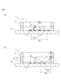
- FIG. 1A is a diagram (part 1) for explaining an overview of a light emitting device according to the present disclosure
- FIG. 2B is a diagram (Part 2) for explaining an overview of a light emitting device according to the present disclosure
- FIG. 1 is a perspective view of a light emitting device according to a first embodiment
- FIG. 3 is a cross-sectional view of the light emitting device taken along line AA' shown in FIG. 2
- FIG. 3 is a characteristic diagram of the light emitting device shown in FIG. 2
- FIG. 3 is an explanatory diagram (part 1) of the thickness of the transparent layer shown in FIG. 2
- FIG. 3 is an explanatory diagram (part 2) of the thickness of the transparent layer shown in FIG.
- FIG. 8 is an explanatory diagram (part 1) of the thickness of the transparent layer shown in FIG. 7;
- FIG. 8 is an explanatory diagram (part 2) of the thickness of the transparent layer shown in FIG. 7;
- It is a top view of the light-emitting device which concerns on 3rd Embodiment.
- It is a top view of the light-emitting device which concerns on 4th Embodiment.
- 11A is a cross-sectional view (part 1) of the light emitting device taken along line CC' shown in FIG. 11, and
- FIG. 12B is a cross section of the light emitting device taken along line CC' shown in FIG. 11; It is a figure (part 2).
- FIG. 13B is a cross-sectional view of the light-emitting device taken along line DD' shown in FIG. 13B; For explaining the relationship between the contact portion where the surface of each of the light guide layer and the diffusion layer contacts the reflector shown in FIG. It is a figure, (a) shows the relationship between the contact portion where the surface of the resin before solidification contacts the reflector and the stretching direction of the resin before solidification, and (b) solidifies at the contact portion C1 shown in (a).
- FIG. 14 is a cross-sectional view of a prototype of a light-emitting device according to a fifth embodiment, (b) is an enlarged cross-sectional view of the vicinity of the upper portion of a reflective frame, and (c) is a first light-emitting element and a second light-emitting device. It is an enlarged cross-sectional view of the vicinity of the element.
- 14 is a graph showing luminance characteristics of light emitted from a light emitting device according to a comparative example and the light emitting device shown in FIG. 13;
- FIG. (a) is a cross-sectional view of a light emitting device according to a sixth embodiment, and (b) is a diagram for explaining the structure of a reflector shown in (a).
- (a) is a cross-sectional view of a light-emitting device according to a first modification
- (b) is a cross-sectional view of a light-emitting device according to a second modification
- (c) is a cross-section of a light-emitting device according to a third modification. It is a figure, (d) is sectional drawing of the light-emitting device concerning a 4th modification, (e) is sectional drawing of the light-emitting device concerning a 5th modification.
- FIG. 11D is a cross-sectional view of a light emitting device according to a ninth modification
- (e) is an enlarged view of a portion indicated by an arrow D in (a)
- (f) is an arrow It is an enlarged view of the part indicated by E
- (g) is an enlarged view of the part indicated by arrow F in (c).
- FIG. 20 is a cross-sectional view of a light-emitting device according to a tenth modification
- FIG. 5 is a diagram showing the relationship between the amount of raw material before solidification of the applied diffusion layer and the amount of chromaticity shift.
- FIG. 21 is a perspective view of a light emitting device according to an eleventh modification
- FIG. 21 is a perspective view of a light emitting device according to a twelfth modification
- FIG. 21 is a perspective view of a light-emitting device according to a thirteenth modification
- It is a figure which shows the manufacturing method of the light-emitting device shown in FIG. 26, (a) is a light emitting element mounting process, (b) is a frame material arrangement process.
- FIG. 1A is a diagram (Part 1) for explaining the outline of the light emitting device according to the present disclosure
- FIG. 1B is a diagram (Part 2) for explaining the outline of the light emitting device according to the present disclosure.
- 1(a) and 1(b) are cross-sectional views of a light emitting device according to the present disclosure.
- the light emitting device 1 has a substrate 10 , a first light emitting element 11 , a second light emitting element 12 , a reflector 13 and a light guide layer 14 .
- the substrate 10 is made of a material having high thermal conductivity, such as ceramics and aluminum, and mounts the first light emitting element 11 and the second light emitting element 12 thereon.
- the first light emitting element 11 and the second light emitting element 12 are a silicone resin containing a phosphor that converts the wavelength of light emitted from the LED die and the LED die and emits light having a first wavelength and a second wavelength. It is a CSP type light emitting device having a sealing material such as.
- the reflector 13 is made of silicone resin containing white particles such as titanium oxide (TiO 2 ), and is arranged to surround the first light emitting element 11 and the second light emitting element 12 .
- the light guide layer 14 is a silicone resin that transmits the light emitted from the first light emitting element 11 and the second light emitting element 12, and fills the area surrounded by the reflector 13. As shown in FIG. In the light emitting device 1, the thickness T between the surface of the LED die of the first light emitting element 11 and the second light emitting element 12 and the surface of the light guide layer 14 is T1 or more and T2 or less. emits light with high brightness.
- the maximum value T2 of the thickness T between the surface of the LED die of the first light emitting element 11 and the surface of the light guide layer 14 is the thickness of the two first light emitting elements arranged with one first light emitting element 11 interposed therebetween.
- T2 LG2/(2tan ⁇ c) (2) is indicated by
- the thickness T between the surface of the LED die of the first light emitting element 11 and the surface of the light guide layer 14 is preferably 1 mm or more and 1.5 mm or less.
- the thickness T between the surface of the LED die of the first light emitting element 11 and the surface of the light guide layer 14 is T1 or more, so that the light emitted from the first light emitting element 11 can be guided. It is emitted over the entire surface of layer 14 . Further, in the light emitting device 1, the thickness T between the surface of the LED die of the first light emitting element 11 and the surface of the light guide layer 14 is T2 or less. It is possible to prevent a decrease in efficiency and an increase in manufacturing costs.
- the height of the LED die of the second light emitting element 12 is the same as the height of the LED die of the first light emitting element 11, and the arrangement pitch of the LED die of the second light emitting element 12 is equal to the arrangement pitch of the LED die of the first light emitting element 11. Same as pitch.
- the light-emitting device 1 employs a CSP type light-emitting element, but may be a chip-on-board (COB) type light-emitting device in which an LED die is mounted on a substrate, and a surface-mounted (SMD) type light-emitting device is mounted. It may be a light emitting device that emits light.
- COB chip-on-board
- SMD surface-mounted
- the light emitting device 2 differs from the light emitting device 1 in that it has a first light emitting element 15 and a light guide layer 16 instead of the first light emitting element 11, the second light emitting element 12 and the light guide layer .
- the first light emitting element 15 is an LED die that emits light having a first wavelength.
- the light guide layer 16 has a phosphor layer 17 and a transparent layer 18 .
- the phosphor layer 17 is a silicone resin containing a phosphor that converts the wavelength of light emitted from the first light emitting element 15 and emits light having a second wavelength.
- the transparent layer 18 is a silicone resin that transmits light emitted from the first light emitting element 15 and the phosphor contained in the phosphor layer 17 .
- the thickness T between the surface of the first light-emitting element 15 and the surface of the light guide layer 16 is T3 or more and T4 or less, thereby suppressing the occurrence of yellow rings.
- the minimum value T3 of the thickness T between the surface of the first light emitting element 15 and the surface of the light guide layer 16 is the thickness between the first light emitting element 15 and the reflector 13 which are arranged adjacent to the reflector 13.
- T3 LB1/tan ⁇ c (3) is indicated by That is, the separation distance LB1 between the first light emitting element 15 arranged adjacent to the reflector 13 and the reflector 13 is shorter than Ttan ⁇ c.
- the thickness T between the surface of the first light-emitting element 15 and the surface of the light guide layer 16 is T3 or more.
- the emitted light is emitted to the outer edge of the surface of the light guide layer 16 inscribed in the reflector 13 .
- the light emitted from the first light emitting element 15 is emitted to the outer edge of the surface of the light guide layer 14 in contact with the reflector 13 , so that the light is emitted from the phosphor contained in the phosphor layer 17 .
- the thickness T between the surface of the first light emitting element 15 and the surface of the light guide layer 16 is T4 or less. It is possible to prevent the manufacturing cost from increasing while preventing the manufacturing cost from being increased.
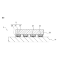
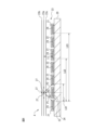
- FIG. 2 is a perspective view of the light emitting device according to the first embodiment
- FIG. 3 is a cross-sectional view taken along line AA' of FIG.
- the light emitting device 3 includes a substrate 20, eight first and second light emitting elements 21 and 22 mounted on the surface of the substrate 20, and arranged above the first and second light emitting elements 21 and 22.
- a sheet-shaped light guide layer 23 is provided. It is more preferable that the upper surface of the sheet-shaped light guide layer 23 is flat. Since the manufacturing method of the light emitting device 3 is well known, detailed description thereof is omitted.
- the substrate 20 is an insulating substrate with high reflectance and thermal conductivity, such as a ceramic or aluminum base substrate, and has power supply electrodes 20a formed at a pair of corners and notches 20b for screwing at the other pair of corners. is formed.
- the first light emitting elements 21 and the second light emitting elements 22 are arranged in a 4 ⁇ 4 matrix on the surface of the substrate 20 . Also, the first light emitting elements 21 and the second light emitting elements 22 are arranged in a checkered pattern.
- the light guide layer 23 is made of silicone resin and arranged to cover the first light emitting element 21 and the second light emitting element 22 .
- the light guide layer 23 does not contain a diffusing material, also called a filler.
- the wiring connecting between the power supply electrode 20a and the first light emitting element 21 and the second light emitting element 22 and between the first light emitting element 21 and the second light emitting element 22 is omitted.
- the first light emitting element 21 and the second light emitting element 22 have a rectangular planar shape of 1.7 mm ⁇ 1.7 mm, and include an LED die 24, a fluorescent resin 25, and a reflective frame 26.
- the LED die 24 and the fluorescent resin 25 included in the first light emitting element 21 are also referred to as the first LED die and the first fluorescent resin
- the LED die 24 and the fluorescent resin 25 included in the second light emitting element 22 are referred to as the second LED die and the second LED die.
- the LED die 24 has a rectangular planar shape of 1.0 mm x 1.0 mm, is a blue diode, and has a sapphire substrate disposed above, a light emitting layer formed below the sapphire substrate, and a bottom surface.
- the fluorescent resin 25 is a silicone resin containing a phosphor such as YAG, covers the surface and side surfaces of the LED die 24 , and converts the wavelength of part of the light emitted from the LED die 24 .
- the reflective frame 26 is made of silicone resin containing reflective fine particles such as titanium oxide, surrounds the fluorescent resin 25, and directs the light emitted from the LED die 24 upward.
- the first light emitting element 21 and the second light emitting element 22 have different content rates of the phosphor contained in the fluorescent resin 25, and emit light having a first wavelength and light having a second wavelength different from the first wavelength. .
- the light having the first wavelength emitted from the first light emitting element 21 is cold light having a color temperature of, for example, 5000K
- the light having the second wavelength emitted from the second light emitting element 22 has a color temperature of, for example, 2700K. It is a warm color light.
- the first light emitting element 21 and the second light emitting element 22 are flip-chip mounted on the surface of the substrate 20 .
- the light guide layer 23 is adhered to the surfaces of the first light emitting element 21 and the second light emitting element 22 with an adhesive.
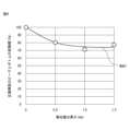
- FIG. 4 is a characteristic diagram showing the relationship between the front luminance of the light emitting device 3 and the thickness of the light guide layer 23.
- the front luminance of the light emitting device 3 is measured along the line AA′ shown in FIG. 2, and the luminance of the light emitted from the first light emitting element 21 and the second light emitting element 22 is adjusted to be the same. .
- the vertical axis of FIG. 4 indicates the fluctuation range between the peak and bottom of the front luminance
- the horizontal axis indicates the thickness (mm) of the light guide layer 23 .
- the front luminance of the light emitted from the light emitting device 3 is maximized directly above the first light emitting element 21 and the second light emitting element 22, and is minimized on the midpoint between the first light emitting element 21 and the second light emitting element 22. become.
- a curve W401 indicates a fluctuation width that is the difference between the peak value (maximum value) and the bottom value (minimum value) of the front luminance.
- the variation width of the front luminance indicated by the curve W401 is normalized with the value when the thickness of the light guide layer 23 is zero, that is, when the light guide layer 23 is not arranged, as 100%.
- the fluctuation width of the front luminance of the light emitted from the first light emitting element 21 and the second light emitting element 22 decreases as the thickness of the light guide layer 23 increases, and changes are small when the thickness of the light guide layer 23 exceeds 1 mm. Become.
- FIG. 5 is an explanatory diagram of an example of the lower limit of the thickness between the surface of the LED die 24 and the surface of the light guide layer 23 of the first light emitting element 21 and the second light emitting element 22, and is shown in FIG. 3 is a cross-sectional view of the light emitting device 3 taken along line -A'; FIG. FIG. 5 is exaggerated such that the distance between the first light emitting element 21 and the second light emitting element 22 is increased.
- the positions of the surface of the light guide layer 23 are shown as a first position 23a, a second position 23b and a third position 23c.
- the first position 23a is the position of the surface of the light guide layer 23 when the lower limit is reached
- the second position 23b is the position of the surface of the light guide layer 23 when the length is longer than the lower limit
- the third position 23c is the position of the surface of the light guide layer 23 when the length is longer than the lower limit. This is the position of the surface of the light guide layer 23 when it is shorter than the lower limit.
- the distance between the LED die 24 of the first light emitting element 21 and the LED die 24 of the adjacent second light emitting element 22 is LG1
- the distance between the LED die 24 of the adjacent first light emitting element 21 is LG2
- the distance between the LED die 24 of the first light emitting element 21 and the LED die 24 of the second light emitting element 22 spaced apart by the first light emitting element 21 and the second light emitting element 22 is LG3.
- a light ray P1 is emitted from the side of the first light emitting element 21 facing the second light emitting element 22 and enters the surface of the light guide layer 23 at the critical angle ⁇ c.
- the light ray P2 is emitted from the side of the second light emitting element 22 facing the first light emitting element 21 and enters the surface of the light guide layer 23 at the critical angle ⁇ c.
- T1 The thickness between the surface of the LED die 24 of the first light emitting element 21 and the second light emitting element 22 and the surface of the light guide layer 23, which is the first position 23a, is denoted by T1.
- the LED die of the first light emitting element 21 and the second light emitting element 22 At an intersection 27 where the median line between 24 and the surface of the light guide layer 23 intersect, the ray P1 and the ray P2 intersect.
- the position of the surface of the light guide layer 23 is the second position 23b, and the thickness between the surface of the LED die 24 of the first light emitting element 21 and the second light emitting element 22 and the surface of the light guide layer 23 is greater than T1. When thick, no dark lines occur. When the thickness between the surface of the LED die 24 of the first light emitting element 21 and the second light emitting element 22 and the surface of the light guide layer 23 is thicker than T1, the light from the surface of the light guide layer 23 to the outside at the intersection 27 .
- the position of the surface of the light guide layer 23 is the third position 23c, and the thickness between the surface of the LED die 24 of the first light emitting element 21 and the second light emitting element 22 and the surface of the light guide layer 23 is T1 When the thickness is thinner than , a belt-like dark portion is generated. When the thickness between the surface of the LED die 24 of the first light emitting element 21 and the second light emitting element 22 and the surface of the light guide layer 23 is less than T1, the surface of the light guide layer 23 is No light is emitted from the
- the thickness between the surface of the LED die 24 of the first light emitting element 21 and the second light emitting element 22 and the surface of the light guide layer 23 is T1 or more, light is emitted from the entire surface of the light guide layer 23. , the uniformity of the brightness of the light emitted from the light emitting device 3 is improved.
- the thickness between the surface of the LED die 24 of the first light emitting element 21 and the second light emitting element 22 and the surface of the light guide layer 23 is T1 or more, light with high luminance uniformity is emitted.
- the brightness of light emitted from the lighting fixture in which the light emitting device 3 is mounted becomes more uniform.
- FIG. 6 is an explanatory diagram of the optimum value and upper limit of the thickness T between the surface of the LED die 24 and the surface of the light guide layer 23 of the first light emitting element 21 and the second light emitting element 22, and
- FIG. 3 is a cross-sectional view of the light emitting device 3 taken along line AA' shown.
- a light ray P1 is emitted from the side of the LED die 24 of the first light emitting element 21 facing the second light emitting element 22, and is incident on the surface of the light guide layer 23 at the critical angle ⁇ c.
- the light ray P3 is emitted from the side facing the second light emitting element 22 of the LED die 24 of the first light emitting element 21 adjacent to the LED die 24 of the first light emitting element 21 that emits the light ray P1 through the second light emitting element 22. , and is incident on the surface of the light guide layer 23 at the critical angle ⁇ c.
- the position of the surface of the light guide layer 23 is the fourth position 23d, and the thickness between the surface of the LED die 24 of the first light emitting element 21 and the second light emitting element 22 and the surface of the light guide layer 23 is T2. At this time, the ray P1 and the ray P3 intersect at the intersection 28 on the surface of the light guide layer 23 .
- the light-emitting device 3 light emitted directly upward from the second light-emitting element 22 is emitted to the outside from the surface of the light guide layer 23 in the vicinity of the intersection 28 on the surface of the light guide layer 23 .
- the light emitting device 3 evenly emits light from the surface of the light guide layer 23 to the outside over the entire surface.
- the refractive index of the light guide layer 23 made of silicone resin is 1.4, and the critical angle ⁇ c is about 45°.
- the distance LG1 between the LED die 24 of the first light emitting element 21 and the LED die 24 of the second light emitting element 22 is 1.0 mm, and the LED die 24 of the first light emitting element 21 and the LED die 24 of the first light emitting element 21 are 1.0 mm. is 3.0 mm.
- T1 calculated by Equation (1) is 0.5 mm.
- T2 calculated by Equation (2) is 1.5 mm.
- the curve W401 becomes saturated when the thickness T of the light guide layer 23 exceeds 1 mm, the amount of change, that is, the amount of attenuation, becomes small.
- the fluctuation width of the front luminance corresponding to the curve W401 is such that the thickness T between the surface of the LED die 24 of the first light emitting element 21 and the second light emitting element 22 and the surface of the light guide layer 23 is two thirds of T2. saturates at the value of
- the value of curve W401 is about 80%. be.
- the value of curve W401 is about 75%. be.
- the thickness T between the surface of the LED die 24 of the first light emitting element 21 and the second light emitting element 22 and the surface of the light guide layer 23 is T1 or more, Brightness uniformity is improved.
- the thickness T between the surface of the LED die 24 and the surface of the light guide layer 23 of the first light emitting element 21 and the second light emitting element 22 is near T1, the uniformity of the brightness of the emitted light It is preferable to provide a diffusion layer above the light guide layer 23 in order to further improve the .
- the thickness T of the light guide layer 23 increases, the luminous efficiency and handleability of the light guide layer 23 decrease.
- the thickness T between the surface of the LED die 24 of the first light emitting element 21 and the second light emitting element 22 and the surface of the light guide layer 23 is 1.0 mm or more, the variation width of the front luminance is saturated.
- the thickness between the surface of the LED die 24 of the first light emitting element 21 and the second light emitting element 22 and the surface of the light guide layer 23 is preferably T1 or more and T2' or less. . Specifically, the thickness T between the surface of the LED die 24 of the first light emitting element 21 and the second light emitting element 22 and the surface of the light guide layer 23 is 0.5 mm or more and 2.5 mm or less. Preferably.
- the light guide layer 23 between the surface of the LED die 24 of the first light emitting element 21 and the second light emitting element 22 and the surface of the light guide layer 23 is preferably thin.
- the optimum thickness T is T2.
- the thickness between the surface of the LED die 24 of the first light emitting element 21 and the second light emitting element 22 and the surface of the light guide layer 23 is 0.5 mm, that is, from the vicinity of (2/3) ⁇ T2, the front luminance is smaller, the thickness T is more preferably (2/3) ⁇ T2 or more and T2′ or less.
- the light-emitting device 3 adjusts the relative intensity of the light emitted from the first light-emitting element 21 and the second light-emitting element 22 so that the light emitted from the first light-emitting element 21 and the light emitted from the second light-emitting element 22 has an intermediate intensity.
- FIG. 7 is a plan view of the light emitting device according to the second embodiment.
- the light emitting device 4 differs from the light emitting device 3 in the number of the first light emitting elements 21 and the second light emitting elements 22 mounted.
- the configuration and functions of the light emitting device 4 other than the numbers of the first light emitting elements 21 and the second light emitting elements 22 to be mounted are the same as the configuration and functions of the light emitting device 3, so detailed description thereof will be omitted here.
- the first light emitting elements 21 and the second light emitting elements 22 are arranged in a 7 ⁇ 7 matrix on the surface of the substrate 20 . Also, the first light emitting elements 21 and the second light emitting elements 22 are arranged in a checkered pattern on the surface of the substrate 20 .
- FIG. 8 is an explanatory diagram of the lower limit of the thickness T between the surface of the LED die 24 and the surface of the light guide layer 23 of the first light emitting element 21 and the second light emitting element 22, and is shown in BB of FIG. 4 is a cross-sectional view of the light emitting device 4 taken along line '.
- the distance between the LED dies 24 of the first light emitting elements 21 adjacent to each other via one second light emitting element 22 is LG1, and the one first light emitting element 21 and the two second light emitting elements 22 are arranged on both sides.
- the distance between the LED dies 24 of the two first light emitting elements 21 is LG2.
- the distance between the LED dies 24 of the first light emitting elements 21 sandwiching the two first light emitting elements 21 and the three second light emitting elements 22 is LG3.
- a light ray P1 is emitted from the side of the LED die 24 of the first light emitting element 21 facing the second light emitting element 22 and enters the surface of the light guide layer 23 at the critical angle ⁇ c.
- the light ray P2 is emitted from the LED die 24 of the first light emitting element 21 that is adjacent to the first light emitting element 21 that emits the light ray P1 via one second light emitting element 22. 2
- the light is emitted from the side facing the light emitting element 22 and enters the surface of the light guide layer 23 at the critical angle ⁇ c.
- the thickness between the surface of the LED die 24 of the first light emitting element 21 and the second light emitting element 22 and the surface of the light guide layer 23, which is the first position 23a, is denoted by T1.
- the thickness T1 between the surface of the LED die 24 of the first light emitting element 21 and the second light emitting element 22 and the surface of the light guide layer 23 is the critical angle ⁇ c when light is emitted from the light guide layer 23 into the air. and the distance LG1 between the LED dies 24 of the first light emitting elements 21 adjacent to each other via one second light emitting element 22 and the relationship represented by the formula (1).
- the position of the surface of the light guide layer 23 is the second position 23b, and the thickness between the surface of the LED die 24 of the first light emitting element 21 and the second light emitting element 22 and the surface of the light guide layer 23 is T1 or more. At some point, the lights emitted from the first light emitting element 21 and the second light emitting element 22 are mixed over the entire surface of the light guide layer 23 .
- the position of the surface of the light guide layer 23 is the third position 23c, and the thickness between the surface of the LED die 24 of the first light emitting element 21 and the second light emitting element 22 and the surface of the light guide layer 23 is greater than T1. When thin, the lights emitted from the first light emitting element 21 and the second light emitting element 22 do not mix in the vicinity of the intersection 27 .
- FIG. 9 is an explanatory diagram of the optimum value and upper limit of the thickness T between the surface of the LED die 24 and the surface of the light guide layer 23 of the first light emitting element 21 and the second light emitting element 22, and
- FIG. 4 is a cross-sectional view of the light emitting device 4 taken along line BB′ shown.
- a light ray P1 is emitted from the side of the LED die 24 of the first light emitting element 21 facing the second light emitting element 22, and is incident on the surface of the light guide layer 23 at the critical angle ⁇ c.
- the light ray P3 emits the light ray P1 of the LED die 24 of the adjacent first light emitting element 21 through one first light emitting element 21 and two second light emitting elements 22 to the first light emitting element 21 emitting the light ray P1.
- the light is emitted from the side facing the second light emitting element 22 on the side of the first light emitting element 21 and enters the surface of the light guide layer 23 at the critical angle ⁇ c.
- the position of the surface of the light guide layer 23 is the fourth position 23d, and the thickness between the surface of the LED die 24 of the first light emitting element 21 and the second light emitting element 22 and the surface of the light guide layer 23 is T2. At this time, the ray P1 and the ray P3 intersect at the intersection 28 on the surface of the light guide layer 23 .
- the thickness T2 between the surface of the LED die 24 of the first light emitting element 21 and the second light emitting element 22 and the surface of the light guide layer 23 is the critical angle ⁇ c and , and the separation distance LG2 between the LED dies 24 of the first light emitting elements 21 adjacent to each other via one first light emitting element 21 and two second light emitting elements 22, and the relationship represented by Equation (2). Since it is preferable that the light guide layer 23 is thin in order to suppress a decrease in luminous efficiency, the light guide layer 23 between the surface of the LED die 24 of the first light emitting element 21 and the second light emitting element 22 and the surface of the light guide layer 23 is preferably thin.
- the optimum thickness T is T2.
- the thickness between the surface of the LED die 24 of the first light emitting element 21 and the second light emitting element 22 and the surface of the light guide layer 23 is T1 or more and T2 or less.
- the color mixing property of the light emitted from the light emitting element 21 and the second light emitting element 22 can be improved.
- FIG. 10 is a plan view of the light emitting device according to the third embodiment.
- the light-emitting device 5 is arranged in a delta manner, and the first light-emitting element 31, the second light-emitting element 32 and the third light-emitting element 33, which respectively emit light having wavelengths corresponding to RGB colors, are arranged as the first light-emitting element 21 and the second light-emitting element. It differs from the light-emitting device 3 in having it instead of the element 22 .
- the configurations and functions of the constituent elements of the light emitting device 5 other than the first light emitting element 31, the second light emitting element 32 and the third light emitting element 33 are the same as those of the constituent elements of the light emitting device 3 denoted by the same reference numerals. , detailed description is omitted here.
- the first light emitting element 31 is formed of silicone resin that contains the blue LED die 24 and a phosphor that emits red light, such as CASN, and covers the blue LED die, and emits red light.
- the dominant wavelength of the red light emitted from the first light emitting element 31 is within the range between 600 nm and 680 nm, and is 660 nm in one example.
- the second light emitting element 32 is made of a silicone resin that contains a blue LED die 24 and a phosphor that emits green light, such as YAG, and covers the blue LED die 24, and emits green light.
- the dominant wavelength of the green light emitted from the second light emitting element 32 is within the range between 500 nm and 570 nm, and is 550 nm in one example.
- the third light emitting element 33 is formed by the blue LED die 24 and emits blue light.
- the dominant wavelength of the blue light emitted from the third light emitting element 33 is within the range between 445 nm and 495 nm, and is 450 nm in one example.
- the LED die 24 included in the first light emitting element 31 is also called a first LED die
- the LED die 24 included in the second light emitting element 32 is also called a second LED die
- the LED die included in the third light emitting element 33 is also called a second LED die. 24 is also referred to as the third LED die.
- the distance between the LED dies 24 of the first light emitting elements 31 arranged adjacently is LG1, and the distance between the LED dies 24 of the first light emitting elements 31 arranged with one first light emitting element 31 interposed therebetween. is LG2.
- the thickness T between the surface of the LED die 24 and the surface of the light guide layer 23 of the first light emitting element 31, the second light emitting element 32 and the third light emitting element 33 is equal to the thickness T of the first light emitting element 31 arranged adjacently. is greater than or equal to T1 calculated from the distance LG1 between the LED dies 24 by the equation (1).
- the first light emitting element 31, the second light emitting element 32 and the third light emitting element 33 are arranged between the surface of the LED die 24 and the surface of the light guide layer 23 with the one first light emitting element 31 interposed therebetween. It is equal to or less than T2 calculated by Equation (2) from the distance LG2 between the two first light emitting elements 31 .
- the thickness T is the distance between the LED dies 24 of the first light emitting elements 31 arranged adjacently in the direction in which the distance between the LED dies 24 of the first light emitting elements 31 arranged adjacently is the shortest. It may be a value equal to or greater than T1 calculated from the distance by Equation (1).
- the thickness T is the distance between the LED dies 24 of the first light emitting elements 31 arranged adjacently in the direction in which the distance between the LED dies 24 of the first light emitting elements 31 arranged adjacently is the longest. It may be a value equal to or less than T2 calculated from the distance by Equation (2).
- the thickness T is such that the first light emitting element 31, the second light emitting element 32, and the third light emitting element 33 are arranged adjacent to each other in the direction in which the distance between the LED die 24 and the LED die 24 is the longest. It may be a value equal to or greater than T1 calculated from the distance between each of the LED dies 24 of the first light emitting element 31, the second light emitting element 32 and the third light emitting element 33 according to Equation (1). In addition, the thickness T is such that the first light emitting element 31, the second light emitting element 32, and the third light emitting element 33 are arranged adjacent to each other in the direction in which the distance between the LED die 24 and the LED die 24 is the shortest.
- the light-emitting device 5 may further include a diffusion layer that is arranged to cover the light guide layer 23 and diffuses the light guided through the light guide layer 23 .
- FIG. 11 is a plan view of the light emitting device according to the fourth embodiment
- FIG. 12(a) is a cross-sectional view (part 1) of the light emitting device along line CC′ shown in FIG. 11, and
- FIG. ) is a cross-sectional view (part 2) of the light-emitting device taken along line CC' shown in FIG. 11.
- FIG. The light emitting device 6 has a substrate 40 , a first light emitting element 41 , a reflector 42 , a light guide layer 43 and a diffusion layer 44 .
- the substrate 40 has a configuration and functions similar to those of the substrate 20 .
- the first light emitting element 41 is formed by a blue LED die and emits blue light.
- the dominant wavelength of the blue light emitted from the first light emitting element 41 is within the range between 445 nm and 495 nm, and is 450 nm in one example.
- the reflector 42 is made of silicone resin containing white particles such as titanium oxide, and is arranged to surround the first light emitting element 41 .
- the light guide layer 43 has a phosphor layer 45 and a transparent layer 46 .
- the phosphor layer 45 is a silicone resin containing a phosphor such as YAG that absorbs light emitted from the first light emitting element 41 and emits yellow light. Silicone resin.
- the transparent layer 46 is a silicone resin that transmits light emitted from the first light emitting element 15 and the phosphor contained in the phosphor layer 17 .
- the diffusion layer 44 is a diffusing agent containing a filler in silicone resin, a sheet containing diffusing particles, coated microparticle powder, a prism, or the like, and preferably has a large amount of forward scattering and little backward scattering.
- the diffusion layer 44 may be a light-transmitting plate whose front surface or back surface is textured.
- the diffuser layer 44 improves the uniformity of brightness and color mixture on the surface of the transparent layer 46 .
- the diffusion layer 44 since light is emitted from the entire surface of the diffusion layer 44, when the light-emitting device 6 is attached to a lighting fixture, the degree of diffusion of the diffusion member provided in the lighting fixture can be reduced, thereby suppressing a decrease in luminous efficiency. Note that the diffusion layer 44 may be omitted.
- the thickness T between the surface of the first light emitting element 41 and the surface of the light guide layer 43 is equal to or greater than T1 calculated from the distance between the first light emitting elements 41 arranged adjacently by Equation (1). be. Moreover, it is less than or equal to T2 calculated by the formula (2) from the distance between the two first light emitting elements 41 arranged with one first light emitting element 41 interposed therebetween.
- the thickness Tk of the diffusion layer 44 is preferably thicker than 0 mm and thinner than the thickness T between the surface of the first light emitting element 41 and the surface of the light guide layer 43 .
- the thickness Tk of the diffusion layer 44 is thicker than 0.3 times the thickness T between the surface of the first light emitting element 41 and the surface of the light guide layer 43 and the surface of the LED die of the first light emitting element 41. More preferably, it is thinner than 0.5 times the thickness T between the surface of the light guide layer 43 .
- the thickness T between the surface of the first light emitting element 41 and the surface of the light guide layer 43 is 1.0 mm or more and 1.5 mm or less, and the thickness of the diffusion layer 44 is 0.5 mm,
- the variation width of the front luminance of the light from the first light emitting element 41 is a good value of 40%.
- the total luminous flux of the light from the first light emitting element 41 is 7.5 mm compared to the case where the diffusion layer 44 is not arranged. %descend.
- the thickness of the light guide layer 43 is 1.25 mm and the thickness of the diffusion layer 44 is 0.5 mm, the total luminous flux of the light from the first light emitting element 41 is , and the decrease in total luminous flux is suppressed more than when the light guide layer 43 is not arranged.
- the thickness T between the surface of the first light emitting element 41 and the surface of the light guide layer 43 is 1.0 mm or more and 1.5 mm or less, and the thickness of the diffusion layer 44 is 0.5 mm
- the thickness Tk of the diffusion layer 44 is included in a range that is thicker than 0.3 times the thickness T and thinner than 0.5 times.
- the thickness Tk of the diffusion layer 44 By making the thickness Tk of the diffusion layer 44 thicker than 0.3 times the thickness T and thinner than 0.5 times the thickness T, the fluctuation range of the front luminance of the light from the first light emitting element 41 can be reduced to can be reduced and the drop in total luminous flux can be suppressed.
- the yellow ring is formed near the inner wall of the reflector 42 without mixing the blue light emitted from the first light emitting element 41 and the yellow light emitted from the phosphor contained in the phosphor layer 45 . This is a phenomenon in which a yellow ring occurs.
- the separation distance between the first light emitting element 41 and the reflecting material 42, which are arranged adjacent to the reflecting material 42, is LB1
- the light ray P4 is emitted from the reflecting material 42 of the first light emitting element 41. and enters the surface of the light guide layer 23 at the critical angle ⁇ c.
- the separation distance LB1 is the minimum distance between the first light emitting element 41 and the reflector 42 that is not surrounded by other first light emitting elements 41 on at least two sides.
- the separation distance between the first light emitting element 41 and the reflecting material 42, which are arranged adjacent to the reflecting material 42 via another first light emitting element 41, is LB2.
- the light ray P5 is emitted from the side facing the reflector 42 of the first light emitting element 41 arranged adjacent to the reflector 42 via another first light emitting element 41, and is emitted from the surface of the light guide layer 23. at the critical angle ⁇ c.
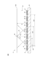
- FIG. 13(a) is a perspective view of the light emitting device according to the fifth embodiment
- FIG. 13(b) is a plan view of the light emitting device shown in FIG. 13(a)
- FIG. It is a cross-sectional view of the light-emitting device taken along line DD' shown.
- the light emitting device 7a has a first light emitting element 21, a second light emitting element 22, a substrate 40a, a reflector 42a, a light guide layer 43a, and a diffusion layer 44a. Since the configurations and functions of the first light emitting element 21 and the second light emitting element 22 have been described with reference to FIGS. 2 and 3, detailed description thereof will be omitted here.
- the substrate 40 a has the same configuration and functions as the substrate 20 .
- the reflective material 42 a is made of silicone resin containing white particles such as titanium oxide, and is arranged to surround the first light emitting element 41 .
- the reflector 42a has a plurality of layers that are superimposed. Specifically, the reflector 42a has a first layer 45a, a second layer 46a, and a third layer 47a.
- the first layer 45a is the bottom layer
- the second layer 46a is the intermediate layer
- the third layer 47a is the top layer.
- the third layer 47a which is the uppermost layer, has a substantially semicircular cross-sectional shape. Since the third layer 47a has a substantially semicircular cross-sectional shape, the reflector 42a has a curved surface formed so as to bulge upward on the upper portion of the inner wall.
- Each of the first layer 45a, the second layer 46a, and the third layer 47a is arranged such that the inner wall and the outer wall stand upright in the vertical direction.
- the reflector according to the embodiment may be formed of a plurality of layers of 2 layers or 4 layers or more.
- the width of each of the multiple layers may be narrower than the width of the multiple layers arranged between each of the multiple layers and the substrate 40a.
- the light guide layer 43a is also referred to as a first light-transmitting layer, is formed of a silicone resin like the light guide layer 23, is arranged to cover the first light emitting element 21 and the second light emitting element 22, and contains a filler. It does not contain a diffusing agent, also called The surface of the light guide layer 43a has an end portion, also referred to as a first contact portion, which contacts the third layer 47a of the reflector 42a, and has a height toward the center of the mounting area where the plurality of first light emitting elements are mounted. has a concave cross-sectional shape with a low
- the diffusion layer 44 a is also called a second light-transmitting layer, and is silicone resin containing a diffusion material that diffuses the light emitted from the first light emitting element 41 .
- the rear surface of the diffusion layer 44a is arranged so as to be in contact with the surface of the light guide layer 43a. It has a concave cross-sectional shape that decreases in height.
- the surface of the light guide layer 43a has an end portion, also referred to as a second contact portion, that contacts the third layer 47a of the reflector 42a, and has a height toward the center of the mounting area where the plurality of first light emitting elements are mounted. has a convex cross-sectional shape in which the
- the diffusion material contained in the diffusion layer 44a is at least one of silica (SiO 2 ) and titanium oxide (TiO 2 ), for example.
- silica silica
- TiO 2 titanium oxide
- the diffusing material contained in the diffusing layer 44a is silica
- the refractive index difference between silica and silicone resin is small.
- the viscosity of the raw material before solidification rises and the coatability deteriorates.
- the diffusing material contained in the diffusing layer 44a is titanium oxide
- the desired degree of scattering can be achieved with a small content of titanium oxide because the difference in refractive index between titanium oxide and silicone resin is large. . This is because when the diffusion material contained in the diffusion layer 44a is titanium oxide, the content of titanium oxide is reduced.
- the luminance and chromaticity of light emitted through the diffusion layer 44a may become non-uniform.
- the content of titanium oxide increases, the amount of return light reflected by the titanium oxide increases, and the luminous efficiency may decrease.
- the diffusion material contained in the diffusion layer 44a is preferably both silica and titanium oxide.
- silica and titanium oxide By containing both silica and titanium oxide as diffusion materials in the diffusion layer 44a, it is possible to form the diffusion layer 44a having a desired degree of scattering while suppressing an increase in the viscosity of the raw material before the diffusion layer 44a is solidified. can.
- the diffusing material contained in the diffusing layer 44a is not limited to silica and titanium oxide.
- a second diffusing material having a composition different from that of the first diffusing material may be used.
- the diffusion layer 44a may contain three or more types of diffusion materials having different compositions.
- FIG. 15 shows the relationship between the contact portion where the surface of each of the light guide layer 43a and the diffusion layer 44a contacts the reflector 42a and the shape of the surface of the resin forming each of the light guide layer 43a and the diffusion layer 44a before solidification. It is a figure for explaining.
- FIG. 15(a) shows the relationship between the contact portion where the surface of the resin before hardening contacts the reflector 42a and the stretching direction of the resin before hardening.
- FIG. 15(b) shows the result of actual measurement showing the cross-sectional shape of the resin before solidification when the surfaces of the resin before solidification come into contact with each other at the contact portion C1 shown in FIG. 15(a).
- FIG. 15 shows the relationship between the contact portion where the surface of each of the light guide layer 43a and the diffusion layer 44a contacts the reflector 42a and the shape of the surface of the resin forming each of the light guide layer 43a and the diffusion layer 44a before solidification. It is a figure for explaining.
- FIG. 15(a) shows the relationship
- FIG. 15(c) is an actual measurement result showing the cross-sectional shape of the resin before solidification when the surface of the resin before solidification comes into contact with the contact portion C2 shown in FIG. 15(a).
- FIG. 15(d) is a result of actual measurement showing the cross-sectional shape of the resin before solidification when the respective surfaces of the resin before solidification come into contact with each other at the contact portion C3 shown in FIG. 15(a).
- FIG. 15(e) is an actual measurement result showing the cross-sectional shape of the resin before solidification when the respective surfaces of the resin before solidification come into contact with each other at the contact portion C4 shown in FIG. 15(a).
- the contact angle of the resin forming the light guide layer 43a and the diffusion layer 44a before solidification with respect to the reflector 42a was 30°.
- a diagram showing the cross-sectional shape of the resin before hardening when the respective surfaces of the resin before hardening come into contact with each other at the contact portion C5 shown in FIG. 15A is omitted.
- the pre-hardened resin When the surface of the pre-hardened resin comes into contact with the contact portion C1 where the inner wall of the reflector 42a extends in the vertical direction, the pre-hardened resin contacts in a direction L1 inclined from the vertical direction by an angle corresponding to the contact angle. It extends from part C1.
- the tangential direction at the contact portion C2 is inclined. It extends from the contact portion C1 in a direction L2 inclined by an angle corresponding to the tangential direction.
- the stretching direction of the resin before solidification becomes closer to the horizontal direction than when the surfaces of the resin before solidification come into contact with each other at the contact portion C1.
- the tangential direction at the contact portion C3 is further inclined, so the resin before solidified extends from the contact portion C2. It extends in a direction L3 closer to the horizontal direction than when it is drawn.
- the stretching direction of the resin before solidification extends in the direction L4 above the horizontal direction.
- the stretch direction of the resin before solidification changes from the vertical downward direction to the horizontal direction according to the increase in the height of the contact portion. direction, over the horizontal direction, and vertically upward direction.
- the height of the resin contact portion of the diffusion layer 44a higher than the height of the resin contact portion of the light guide layer 43a, it is possible to make the stretching directions of the respective surfaces of the light guide layer 43a and the diffusion layer 44a different. be possible.
- the thickness of the light guide layer 43a increases as the distance from the second contact portion increases.
- the thickness of the light guide layer 43a at the center of the mounting area where the first light emitting element 21 and the second light emitting element 22 are mounted becomes thicker as the distance from the second contact portion increases, and the surface of the contact portion contacts the reflector 42a. can be thicker than the thickness of the light guide layer 43a in . Also, the thickness of the central portion of the resin before solidification when the respective surfaces of the resin before solidification come into contact at the contact portion C5 shown in FIG. It is even thicker than the central thickness of FIG. 15(e), which shows the cross-sectional shape of the resin before solidification when the respective surfaces of the previous resin come into contact.
- Each of the contact portions C1 to C4 is an example of a first contact portion in which the upper end of the light guide layer 43a is in contact with the reflector 42a.
- each of the contact portions C2 to C5 is an example of a second contact portion in which the upper end of the diffusion layer 44a is in contact with the curved surface of the reflector 42a.
- a lower end P0 of the inner wall of the reflector 42a is a portion where the inner wall of the reflector 42a contacts the substrate 40a.
- the contact portion C2 is the second contact portion where the upper end of the diffusion layer 44a contacts the curved surface of the reflector 42a
- the contact portion C2 is the second contact where the upper end of the diffusion layer 44a contacts the curved surface of the reflector 42a.
- a horizontal separation distance between the portion C2 and the lower end P0 of the inner wall of the reflector 42a is W1.
- the horizontal separation distance W1 between the contact portion C2, which is the second contact portion, and the lower end P0 of the inner wall of the reflector 42a is the distance between the contact portion C1, which is the first contact portion, and the lower end P0 of the inner wall of the reflector 42a. greater than "zero" horizontal separation between
- the horizontal direction between the contact portions C1 and C2 and the lower end P0 of the inner wall of the reflector 42a is "zero" and W1.
- the contact portion C3 is the second contact portion where the upper end of the diffusion layer 44a is in contact with the curved surface of the reflector 42a
- the horizontal separation distance between the contact portion C3 and the lower end P0 of the inner wall of the reflector 42a is W2.
- a horizontal separation distance W2 between the contact portion C3, which is the second contact portion, and the lower end P0 of the inner wall of the reflector 42a is the contact portions C1 and C2, which are the first contact portions, and the lower end P0 of the inner wall of the reflector 42a. and the horizontal separation distance "zero" between and greater than W1.
- any one of the contact portions C1 to C3 is the first contact portion in which the upper end of the light guide layer 43a is in contact with the reflector 42a
- the horizontal direction between the contact portions C1 to C3 and the lower end P0 of the inner wall of the reflector 42a are "zero", W1 and W2.
- the contact portion C4 is the second contact portion where the upper end of the diffusion layer 44a is in contact with the curved surface of the reflector 42a
- the horizontal separation distance between the contact portion C4 and the lower end P0 of the inner wall of the reflector 42a is W3 is.
- a horizontal separation distance W3 between the contact portion C4, which is the second contact portion, and the lower end P0 of the inner wall of the reflector 42a is the distance between the contact portions C1 to C3, which are the first contact portions, and the lower end P0 of the inner wall of the reflector 42a. is greater than W1 and W2.
- any one of the contact portions C1 to C4 is the first contact portion in which the upper end of the light guide layer 43a is in contact with the reflector 42a
- the horizontal direction between the contact portions C1 and C2 and the lower end P0 of the inner wall of the reflector 42a are "zero", W1, W2 and W3.
- the contact portion C5 is the second contact portion where the upper end of the diffusion layer 44a is in contact with the curved surface of the reflector 42a
- the horizontal separation distance between the contact portion C5 and the lower end P0 of the inner wall of the reflector 42a is W4 is.
- a horizontal separation distance W4 between the contact portion C5, which is the second contact portion, and the lower end P0 of the inner wall of the reflector 42a is the distance between the contact portions C1 to C4, which are the first contact portions, and the lower end P0 of the inner wall of the reflector 42a. is greater than W1, W2 and W3.
- FIG. 16 is a flow chart showing a method for manufacturing the light emitting device 7a.
- the substrate 40a is prepared (S101).
- the first light emitting element 21 and the second light emitting element 22 are mounted on the substrate 40a (S102).
- a wire bonding step each of the first light emitting element 21 and the second light emitting element 22 is electrically connected to each of two pairs of anode electrodes and cathode electrodes arranged on the substrate 40a through bonding wires (not shown). connected (S103).
- the reflector 42a is arranged so as to surround the first light emitting element 21 and the second light emitting element 22 (S104).
- the raw material before solidification of the first layer 45a is placed, then the raw material before solidification of the second layer 46a is placed, and then the raw material before solidification of the third layer 47a is placed.
- the substrate 40a is heated, the raw materials of the first layer 45a, the second layer 46a and the third layer 47a are solidified to form the reflector 42a.
- the first contact portion which is the edge of the surface of the light guide layer 43a, contacts the reflector 42a at the third layer 47a. can be filled with the resin before solidification of the light guide layer 43a.
- the light guide layer 43a is placed (S105). First, the raw material of the light guide layer 43a before solidification is arranged. Next, the light guide layer 43a is formed by solidifying the raw material of the light guide layer 43a as the substrate 40a is heated.
- the diffusion layer 44a is placed (S106), thereby completing the manufacturing process of the light emitting device 7a.
- the raw material of the diffusion layer 44a before solidification is applied on the light guide layer 43a by spraying.
- the diffusion layer can be formed regardless of whether the surface of the light guide layer 43a has a flat shape, an upwardly curved convex shape, or a downwardly curved concave shape. 44a is formed.
- FIG. 17(a) is a sectional view of a prototype of the light emitting device 7a according to the fifth embodiment.
- 17B is an enlarged cross-sectional view of the vicinity of the upper portion of the reflector 42a
- FIG. 17C is an enlarged cross-sectional view of the vicinity of the first light emitting element 21 and the second light emitting element 22.
- FIG. 17B is an enlarged cross-sectional view of the vicinity of the upper portion of the reflector 42a
- FIG. 17C is an enlarged cross-sectional view of the vicinity of the first light emitting element 21 and the second light emitting element 22.
- the thickness T between the surface of the first light emitting element 21 and the bottom of the surface of the light guide layer 43a is is greater than or equal to T1 calculated by the formula (1) from the distance between
- the thickness T between the surface of the second light emitting element 22 and the bottom of the surface of the light guide layer 43a is calculated from the distance between the second light emitting elements 22 arranged adjacent to each other by Equation (1). is equal to or greater than T1.
- the height H3 from the surface of the substrate 40a to the bottom of the surface of the light guide layer 43a is lower than the height H2 of the reflector 42a.
- the height (H3+H4) from the surface of the substrate 40a to the top of the surface of the diffusion layer 44a is higher than the height H2 of the reflector 42a.
- the surface of the first light-emitting element 21 and the light guide layer between the first light-emitting element 21 and the second light-emitting element 22 arranged adjacent to the reflector 42a and the reflector 42a The thickness T between the bottom of the surface of 43a is thicker than T3 calculated by equation (3).
- the separation distance LB1 in Expression (3) is the separation distance between the first light emitting element 21 and the second light emitting element 22 arranged adjacent to the reflector 42a and the reflector 42a.
- the thickness of the light guide layer 43a becomes thinner as the distance from the first contact portion increases.
- the thickness of the light guide layer 43a becomes thinner as the distance from the first contact portion increases.
- the thickness is thinner than the thickness of the light guide layer 43a in the first contact portion.
- the height of the second contact portion where the upper end of the diffusion layer 44a contacts the curved surface of the reflector 42a is higher than the height of the first contact portion where the upper end of the light guide layer 43a contacts the reflector 42a. Therefore, the thickness of the diffusion layer 44a increases as the distance from the reflector 42a increases.
- the thickness of the diffusion layer 44a increases with increasing distance from the reflector 42a, the thickness of the diffusion layer 44a is the thickest in the central portion of the mounting area where the density of the first light emitting elements 21 and the second light emitting elements 22 is high. In addition, the thickness of the diffusion layer 44a is the thinnest in the outer edge portion of the mounting area where the density of the first light emitting elements 21 and the second light emitting elements 22 is low.
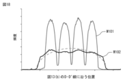
- FIG. 18 is a diagram showing luminance characteristics of light emitted from a light emitting device and a light emitting device 7a according to a comparative example.
- the horizontal axis indicates the position between the reflectors 42a in the cross section along line DD' of FIG. 13(b), and the vertical axis indicates the luminance.
- W101 indicates the luminance characteristic of a light emitting device having a light guide layer with a flat surface and no diffusion layer
- W102 indicates the luminance characteristic of the light emitting device 7a.
- the brightness of the region where the light-emitting element is arranged is high, while the brightness of the region where the light-emitting element is not arranged is low. large difference in brightness.
- the maximum luminance value is about 1/3 of the luminance of the light-emitting device having no diffusion layer, the luminance uniformity is improved.
- the first contact portion which is the edge of the surface of the light guide layer 43a, contacts the reflector 42a at the third layer 47a.
- the pre-hardened resin of the light guide layer 43a can be filled.
- the edge of the surface of the light guide layer 43a is in contact with the reflector 42a at the second layer 46a, the third layer 47a is arranged after the light guide layer 43a is formed. Can be simplified.
- FIG. 19(a) is a cross-sectional view of the light emitting device according to the sixth embodiment
- FIG. 19(b) is a diagram for explaining the structure of the reflector shown in FIG. 19(a).
- FIG. 19(a) is a cross-sectional view corresponding to the cross-sectional view along line DD' shown in FIG. 13(b).
- the light emitting device 7b differs from the light emitting device 7a in that it has a reflector 42b, a light guide layer 43b and a diffusion layer 44b instead of the reflector 42a, the light guide layer 43a and the diffusion layer 44a.
- the configurations and functions of the components of the light-emitting device 7b other than the reflector 42b, the light guide layer 43b, and the diffusion layer 44b are the same as those of the components of the light-emitting device 7a denoted by the same reference numerals. Description is omitted.
- the reflector 42b is made of silicone resin containing white particles such as titanium oxide, and has a first layer 45b, a second layer 46b, and a third layer 47b.
- Each of the first layer 45b, the second layer 46b, and the third layer 47b has a spherically curved surface, and the first layer 45b, the second layer 46b, and the third layer 47b are stacked in this order. be.
- the third layer 47b is arranged such that the position of the apex in top view is located outside the position of the apex of the second layer 46b.
- the first contact portion which is the end portion of the light guide layer 43b, contacts the curved surface of the second layer 46b arranged below the third layer 47b, which is the uppermost layer, and the second contact portion, which is the end portion of the diffusion layer 44b. contact the curved surface of the third layer 47b.
- the light guide layer 43b is also called a first light-transmitting layer like the light guide layer 43a, and differs from the light guide layer 43a in that its surface extends in the horizontal direction.
- the thickness of the light guide layer 43b at the center of the mounting area where the first light emitting element 21 and the second light emitting element 22 are mounted is equal to the thickness of the light guide layer 43b at the first contact portion.
- the configuration and function of the light guide layer 43b are the same as the configuration and function of the light guide layer 43a except for the extension direction of the surface, so detailed description thereof will be omitted here.
- the diffusion layer 44b is also referred to as a second light-transmitting layer like the diffusion layer 44a, and differs from the diffusion layer 44a in that its surface extends in the horizontal direction.
- the configuration and function of the diffusion layer 44b are the same as the configuration and function of the diffusion layer 44a except for the extending direction of the surface, so detailed description thereof will be omitted here.
- the height of the first contact portion which is the outer edge of the light guide layer 43b
- the height of the second contact portion which is the outer edge of the diffusion layer 44b
- the thickness of the diffusion layer 44b at the center of the mounting area where the first light emitting element 21 and the second light emitting element 22 are mounted is the first It is equal to the thickness of the diffusion layer 44b at the contact portion.
- FIG. 20(a) is a cross-sectional view of a light emitting device according to a first modification
- FIG. 20(b) is a cross-sectional view of a light emitting device according to a second modification
- FIG. 20(c) is a third modification
- 2 is a cross-sectional view of a light emitting device according to FIG.
- FIG. 20(d) is a cross-sectional view of a light emitting device according to a fourth modification
- FIG. 20(e) is a cross-sectional view of a light emitting device according to a fifth modification.
- 20(a) to 20(e) are cross-sectional views corresponding to cross-sectional views taken along line AA' shown in FIG.
- the light-emitting device 8a according to the first modification differs from the light-emitting device 3 in that it has a reflector 50 and a light guide layer 51 instead of the light guide layer 23 .
- the configurations and functions of the components of the light-emitting device 8a other than the reflector 50 and the light guide layer 51 are the same as those of the components of the light-emitting device 3 denoted by the same reference numerals, and detailed descriptions thereof are omitted here. .
- the reflector 50 is made of silicone resin containing white particles such as titanium oxide, like the reflector 42 , and is arranged to surround the first light emitting element 21 and the second light emitting element 22 .
- the light guide layer 51 is silicone resin filled in the area surrounded by the reflector 50 and transmits light emitted from the first light emitting element 21 and the second light emitting element 22 .
- the light guide layer 51 is formed by heating the substrate 20 after the reflecting material 50 is filled with the unhardened resin material, thereby solidifying the unhardened resin material.
- the light emitting device 8 a can emit light with high directivity from the surface of the light guide layer 51 by having the reflector 50 .
- the light-emitting devices 3 to 5 do not have a reflector, but are arranged on the substrate so as to surround the plurality of first light-emitting elements, and further include a reflector for reflecting the light emitted from the first light-emitting elements. good too.
- a light-emitting device 8b according to the second modification differs from the light-emitting device 8a in that it has a diffusion layer 52 .
- the configurations and functions of the constituent elements of the light emitting device 7b other than the diffusion layer 52 are the same as those of the constituent elements of the light emitting device 8a to which the same reference numerals are assigned, so detailed descriptions thereof are omitted here.
- the diffusion layer 52 is a sheet containing diffusion particles, coated microparticle powder, prisms, or the like. 51. Since the light emitting device 8b has the diffusion layer 52, it is possible to emit light with high luminance uniformity and high color mixing. Although the light emitting devices 3 to 5 do not have a diffusion layer, they may further include a diffusion layer arranged to cover the light guide layer and diffusing the light guided through the light guide layer.
- the light-emitting device 8c according to the third modification differs from the light-emitting device 8b in that it has a diffusion layer 53 instead of the diffusion layer 52.
- the configurations and functions of the constituent elements of the light emitting device 8c other than the diffusion layer 53 are the same as those of the constituent elements of the light emitting device 8b to which the same reference numerals are attached, so detailed descriptions thereof are omitted here.
- the diffusion layer 53 differs from the diffusion layer 52 in that diffusion portions 53 a are formed above the first light emitting element 21 and the second light emitting element 22 .
- the diffuser 53a is formed above the first light emitting element 21 and the second light emitting element 22 emitting light with high brightness, so that the light with high brightness is efficiently mixed to emit light. It is possible to emit light with high luminance uniformity and color mixing while suppressing a decrease in efficiency.
- a light-emitting device 8d according to the fourth modification differs from the light-emitting device 8b in that it has a light guide layer 54 and a diffusion layer 55 instead of the light guide layer 51 and the diffusion layer 52 .
- the configurations and functions of the constituent elements of the light emitting device 8d other than the light guide layer 54 and the diffusion layer 55 are the same as those of the constituent elements of the light emitting device 8b denoted by the same reference numerals, and detailed descriptions thereof are omitted here. .
- the light guide layer 54 differs from the light guide layer 51 in that the shape of the surface thereof is convexly curved.
- the diffusion layer 55 is different from the diffusion layer 53 in that it has a curved shape in which the central portion protrudes upward according to the shape of the surface of the light guide layer 54 .
- the light guide layer 54 and the diffusion layer 55 have a curved lens shape such that the central portion protrudes upward, so that light with high directivity can be emitted.
- a light-emitting device 8e according to the fifth modification differs from the light-emitting device 8a in that it has a frame member 56 and an adhesive layer 57 instead of the reflector 50 and the light guide layer 51 .
- the configurations and functions of the constituent elements of the light emitting device 8e other than the frame member 56 and the adhesive layer 57 are the same as those of the constituent elements of the light emitting device 8a denoted by the same reference numerals, and detailed descriptions thereof are omitted here.
- the frame member 56 has a diffusion frame 58 and a light guide portion 59.
- the diffusion frame 58 has a side part arranged to surround the first light emitting element 21 and the second light emitting element 22, and an upper part covering the first light emitting element 21 and the second light emitting element 22. Light emitted from the light emitting element 21 and the second light emitting element 22 is diffused and emitted to the outside.
- the side surface of the diffusion frame that covers the side surface of the light guide section 59 is thicker than the diffusion section that covers the surface of the light guide section, and functions as a reflection frame.
- the light guide part 59 is formed of a member such as silicone resin that transmits light emitted from the first light emitting element 21 and the second light emitting element 22 , and is integrated with the diffusion frame 58 .
- the adhesive layer 57 is formed of a material such as silicone resin that transmits light emitted from the first light emitting element 21 and the second light emitting element 22 , and is an adhesive member that bonds the frame member 56 to the substrate 20 .
- the frame member 56 has the diffusion frame 58 and the light guide portion 59, so that no reflective material, which is also called a dam material, is arranged, so that the manufacturing process can be simplified.
- the diffusion frame 58 and the light guide section 59 are integrated by the frame member 56, so it is easy to manufacture the light guide section 59 with a uniform thickness.
- by adjusting the degree of diffusion of the diffusion frame 58 it is possible to easily form a diffusion layer having a desired degree of diffusion.
- the frame material 56 functions as a reflective frame by increasing the thickness of the side surface of the light guide section 59 . may be placed.
- FIG. 21(a) is a cross-sectional view of a light emitting device according to a sixth modification
- FIG. 21(b) is a cross-sectional view of a light emitting device according to a seventh modification
- FIG. 21(c) is an eighth modification
- 21D is a cross-sectional view of a light-emitting device according to a ninth modification.
- FIG. 21(e) is an enlarged view of the portion indicated by arrow D in FIG. 21(a)
- FIG. 21(f) is an enlarged view of the portion indicated by arrow E in FIG. 21(b)
- FIG. ) is an enlarged view of a portion indicated by an arrow F in FIG. 21(c).
- 21(a) to 21(d) are cross-sectional views corresponding to cross-sectional views taken along line AA' shown in FIG.
- the light emitting device 8f differs from the light emitting device 8b in that it has a white resin 60.
- the configuration and function of the constituent elements of the light emitting device 8f other than the white resin 60 are the same as the configuration and function of the constituent elements of the light emitting device 8b denoted by the same reference numerals, so detailed description thereof will be omitted here.
- the white resin 60 is made of silicone resin containing white particles such as titanium oxide, like the reflector 42 , and is arranged between the first light emitting element 21 and the second light emitting element 22 .
- the white resin 60 is arranged between the first light emitting element 21 and the second light emitting element 22, thereby suppressing the amount of light absorbed by the substrate 40 and improving the light emitting efficiency.
- the reflector 50 and the diffusion layer 53 may be omitted.
- the light-emitting device 8g differs from the light-emitting device 8f in that it has a first light-emitting element 61 and a second light-emitting element 62 instead of the first light-emitting element 21 and the second light-emitting element 22 .
- the configurations and functions of the constituent elements of the light emitting device 8g other than the first light emitting element 61 and the second light emitting element 62 are the same as those of the constituent elements of the light emitting device 8f to which the same reference numerals are attached, so detailed description thereof will be omitted here. are omitted.
- the first light emitting element 61 and the second light emitting element 62 are arranged so that the sides of the fluorescent resin of the first light emitting element 61 and the second light emitting element 62 do not stand upright and open upward and outward. It is different from the first light emitting element 21 and the second light emitting element 22 .
- the white resin 60 is arranged between the first light-emitting element 61 and the second light-emitting element 62, so that the white resin 60 functions as a reflector and can further improve the luminous efficiency. Note that the reflector 50 and the diffusion layer 53 may be omitted.
- the light emitting device 8h differs from the light emitting device 8f in that it has a white resin 60a instead of the white resin 60. Further, the light emitting device 8h differs from the light emitting device 8f in having a transparent resin 60b.
- the configurations and functions of the constituent elements of the light emitting device 8h other than the white resin 60a and the transparent resin 60b are the same as those of the constituent elements of the light emitting device 8f denoted by the same reference numerals, so detailed description thereof will be omitted here.
- the white resin 60a differs from the white resin 60 in that a concave portion is formed between the first light emitting element 21 and the second light emitting element 22 in which the transparent resin 60b is arranged.
- the structure and function of the white resin 60a are the same as those of the white resin 60, except for the formation of the concave portion, so detailed description thereof will be omitted here.
- the transparent resin 60 b is arranged between the first light emitting element 21 and the second light emitting element 22 and the white frame 63 .
- the transparent resin 60b is arranged along the side surface of the fluorescent resin 25 of the first light emitting element 21 and the second light emitting element 22 so that the side surface opens upward and outward.
- the light emitting device 8i differs from the light emitting device 8f in that it has a white frame 63 and a frame material 64 instead of the reflector 50, the light guide layer 51, the diffusion layer 52 and the white resin 60.
- the configurations and functions of the constituent elements of the light emitting device 8i other than the white frame 63 and the frame member 64 are the same as those of the constituent elements of the light emitting device 8f denoted by the same reference numerals, so detailed description thereof will be omitted here.
- the white frame 63 is made of a white resin material having higher rigidity than the white resin 60, and has a plurality of insertion holes into which the first light emitting element 21 and the second light emitting element 22 are respectively inserted.
- the frame member 64 has a light guide layer 65 and a diffusion layer 66 adhered to the light guide layer 65 .
- the light guide layer 65 is a transparent sheet that transmits the light emitted from the first light emitting element 21 and the second light emitting element 22, and the diffusion layer 66 is the light emitted from the first light emitting element 21 and the second light emitting element 22. It is a diffusion sheet that diffuses light.
- FIG. 22 is a cross-sectional view of a light-emitting device according to a tenth modification.
- the light emitting device 6 a differs from the light emitting device 6 in that it has a light guide layer 47 instead of the light guide layer 43 .
- the configurations and functions of the constituent elements of the light-emitting device 6a other than the light guide layer 47 are the same as the configurations and functions of the constituent elements of the light-emitting device 6 denoted by the same reference numerals, and therefore detailed description thereof is omitted here.
- the light guide layer 47 differs from the light guide layer 43 in that it has a phosphor layer 48 instead of the phosphor layer 45 .
- the phosphor layer 48 is unevenly distributed near the periphery of the first light emitting element 41 .
- the phosphor layer 48 is formed by phosphor sedimentation, coating, electrophoresis, or the like.
- the thickness T between the surface of the first light emitting element 41 and the surface of the light guide layer 47 is equal to or greater than T1 calculated from the distance between the first light emitting elements 41 arranged adjacently by Equation (1). be. Also, from the distance between the two first light emitting elements 41 arranged with one first light emitting element 41 sandwiched between the surface of the first light emitting element 41 and the surface of the light guide layer 23, from the formula (2) It is equal to or less than the calculated T2.
- the light emitting device 6 a transmits light emitted from the first light emitting element 41 and light emitted from the phosphor contained in the phosphor layer 48 unevenly distributed around the first light emitting element 41 through the transparent layer 46 . By emitting light, it is possible to emit light with high color mixing.
- the light emitting device 6a may be manufactured by a manufacturing method similar to the manufacturing method of the light emitting device 7a.
- the substrate 40 is prepared in the substrate preparation step.
- the first light emitting element 41 is mounted on the substrate 40 .
- each of the first light emitting elements 41 is electrically connected to each of a pair of anode and cathode electrodes arranged on the substrate 40 via bonding wires (not shown).
- the reflector arrangement step the reflector 42 is arranged so as to surround the first light emitting element 41 .
- the light guide layer placement step the light guide layer 47 is placed.
- the diffusion layer arrangement step the diffusion layer 44 is arranged, thereby completing the manufacturing process of the light emitting device 6a.
- the chromaticity of the light emitted from the light emitting device 6a may be adjusted. After the light guide layer arranging step of arranging the light guide layer 47 is completed and before the diffusion layer arranging step, the light emitted from the transparent layer 46 in response to the current being supplied to the first light emitting element 41 is measured.
- the thickness of the light guide layer 47 to be placed is then determined according to the difference between the measured chromaticity and the desired chromaticity.
- the diffusion layer 44 is formed by solidifying the raw material of the diffusion layer 44 applied by spraying or the like before solidification, the amount of the diffusion layer 44 to be applied before solidification is determined.
- the thickness of the optic layer 47 is determined.
- the amount of raw material applied to the diffusion layer 44 before solidification is determined by referring to a table showing the relationship between the amount of the raw material applied to the diffusion layer 44 before solidification and the amount of chromaticity shift.
- FIG. 23 is a diagram showing the relationship between the amount of raw material applied to the diffusion layer 44 before solidification and the amount of chromaticity shift.
- the thickness of the diffusion layer 44 to be formed is increased.
- the amount of return light reflected by the diffusion layer 44 and transmitted through the phosphor layer 48 increases.
- the amount of return light that passes through the phosphor layer 48 increases, the amount of light that is wavelength-converted from blue to yellow by the phosphor contained in the phosphor layer 48 increases.
- the chromaticity of the light emitted from the light emitting device 6a shifts.
- the diffusion layer 44 is arranged so as to reduce the thickness of the light emitted from the light emitting device 6a to the desired chromaticity.
- the diffusion layer 44 is arranged so as to be thick.
- the degree of freedom in adjusting the chromaticity of the emitted light according to the thickness of the diffusion layer 44 formed is improved.
- FIG. 24 is a perspective view of a light-emitting device according to the eleventh modification.
- the light emitting device 9 has a substrate 70 , a first light emitting element 71 , a light guide layer 72 and a connector 73 .
- the substrate 70 is, for example, a glass epoxy substrate, and wiring patterns for connecting the first light emitting element 71 and the connector 73 are formed.
- the first light-emitting elements 71 are SMD-type light-emitting elements and are arranged in a 4 ⁇ 4 matrix in the central portion of the surface of the substrate 70 .
- the light guide layer 72 is made of silicone resin and arranged to cover the first light emitting element 71 .
- the thickness of the light guide layer 72 that is, the thickness between the surface of the LED die of the first light emitting element 71 and the surface of the light guide layer 72 varies from the distance between the adjacently arranged first light emitting elements 71 to It is equal to or greater than T1 calculated by Equation (1). Also, the distance between the two first light emitting elements 71 sandwiching one first light emitting element 71 between the surface of the LED die of the first light emitting element 71 and the surface of the light guide layer 72 is calculated by the formula ( 2) is equal to or less than T2 calculated by 2).
- the light-emitting device 9 uses SMD-type light-emitting elements and can achieve optical characteristics similar to those of a COB-type light-emitting device.
- the light emitting device 9 has a plurality of electronic components mounted on the substrate 70, and further includes a control circuit for controlling light emission of the plurality of first light emitting elements, etc., thereby enabling various controls such as dimming.
- Light emitting devices can be implemented on a single substrate.
- FIG. 25 is a perspective view of a light emitting device according to a twelfth modification.
- the light-emitting device 9 a has a substrate 80 , a first light-emitting element 81 , a second light-emitting element 82 , a frame member 83 , and an electronic component 84 .
- the substrate 80 is an aluminum base substrate or a CEM3 substrate, on which a pair of electrodes 80a are arranged, and wiring that connects the first light emitting element 81, the second light emitting element 82, the electronic component 84, and the pair of electrodes 80a.
- a pattern is formed.
- the first light emitting element 81 and the second light emitting element 82 are CSP type light emitting elements, and emit cold and warm colors.
- the frame member 83 has a reflective portion 85 and a light guide portion 86 that is a light guide layer integrally formed with the reflective portion 85 .
- the reflective part 85 is a frame member made of a synthetic resin that reflects the light emitted from the first light emitting element 81 and the second light emitting element 82 , and surrounds the first light emitting element 81 and the second light emitting element 82 . placed.
- the light guide part 86 is a frame member made of a synthetic resin that transmits light emitted from the first light emitting element 81 and the second light emitting element 82 , and covers the first light emitting element 81 and the second light emitting element 82 . placed in
- the electronic components 84 include resistors, capacitors, MOSFETs, semiconductor devices, etc., and implement various controls such as flicker suppression and dimming.
- FIG. 26 is a perspective view of a light emitting device according to the thirteenth modification.
- the light-emitting device 9 b has a substrate 90 , a first light-emitting element 91 , a frame member 92 , a white resin 93 , and a transparent layer 94 .
- the substrate 90 is a glass epoxy substrate, an aluminum base substrate, or a CEM3 substrate, like the substrate 80, and has a pair of electrodes 90a arranged thereon, and a wiring connecting between the first light emitting element 91 and the pair of electrodes 90a. A pattern is formed.
- the first light emitting element 91 is a blue diode and emits blue light.
- the frame member 92 is a white frame-shaped member and is arranged to surround the first light emitting element 91 .
- the white resin 93 is a white resin and is arranged so as to surround each of the first light emitting elements 91 .
- the white resin 93 is higher than the height of the first light emitting element 91 .
- the translucent layer 94 is silicone resin containing phosphor.
- the phosphor contained in the translucent layer 94 may be a single phosphor or two types of phosphors. When the translucent layer 94 contains two types of phosphors, the two types of phosphors may be arranged separately so as to correspond to the first light emitting elements 91 respectively.
- FIG. 27A and 27B show a method of manufacturing the light emitting device 9b, wherein FIG. 27(a) shows a light emitting element mounting process and FIG. 27(b) shows a frame member arranging process.
- the first light emitting element 91 is mounted on the substrate 90 in the light emitting element mounting process.
- the frame material placement step the integrally molded frame material 92 and the white resin 93 are placed on the substrate 90 .
- the light-transmitting layer forming step the light-transmitting layer 94 is formed.
- the light-transmitting layer 94 is formed by filling the inside of the frame member 92 with resin before the light-transmitting layer 94 is solidified and then heating the substrate 90 .
- the first light-emitting element 21 and the second light-emitting element 22 are CSP-type light-emitting elements and the diffusion layer 44a is arranged.
- a blue light emitting element and a phosphor layer may be arranged instead of the layer 44a.
- the light-emitting device can be a remote phosphor structure-type light-emitting device.
- the phosphor contained in the resin may be allowed to settle before solidification, and the phosphor may be arranged at the interface with the light-transmitting layer.
- the phosphor layer is arranged on the surface of the blue LED die 24 in each of the first light emitting element 21 and the second light emitting element 22, the phosphor layer is arranged on the surface of the blue LED die 24 by electrostatic coating. You may When the phosphor layer is arranged on the surface of the blue LED die 24 by electrostatic coating, the electrode of the blue LED die 24 that is flip-chip connected is grounded to prevent electrostatic breakdown of the blue LED die 24. can be prevented. When disposing the phosphor layer on the surface of the blue LED die 24 by electrostatic coating, the electrostatic coating process may be performed on the mounting substrate, and after the electrostatic coating on the coating substrate, the blue phosphor layer is deposited on the mounting substrate. An LED die 24 may be mounted.
- the light emitting device can emit light with high color mixing while suppressing the amount of decrease in luminous flux by arranging the light guide layer having a predetermined thickness between the light emitting element and the diffusion layer. can.
- the light emitting device can suppress the fluctuation range of the luminance of the emitted light by about 20% to 30% compared to the case without the light guide layer.
- the light-emitting device includes the diffusion layer in addition to the light guide layer, so that the light emission can be suppressed by about 40% to 60% compared to the case without the light guide layer.
- the light emitting device has a light guide layer, so that the fluctuation range of the chromaticity of the emitted light is suppressed by about 3% to 30% compared to the case without the light guide layer. be able to.
- the light-emitting device includes the diffusion layer in addition to the light guide layer, so that the light emission can be suppressed by about 45% to 75% compared to the case without the light guide layer.
- the light guide layer is made of silicone resin, but in the light emitting device according to the present disclosure, the light guide layer is made of synthetic resin such as epoxy resin, polymethyl methacrylate resin, polycarbonate resin and polystyrene resin. You may form with resin. Further, in the light emitting device described, the light guide layer is formed of a single resin, silicone resin, but may be formed by laminating a plurality of synthetic resins having different refractive indices. When the light guide layer is formed by laminating a plurality of synthetic resins having different refractive indices, the thickness of the light guide layer is determined by calculating the formulas (1) to (4) for each resin layer. be.
- the reflective layer may be formed by a plurality of reflective layers arranged to overlap the substrate.
- the central portion of the reflective layer arranged at the top may be arranged outside the central portions of the other reflective layers.
- the central part of the reflective layer, which is arranged at the top, is arranged outside the central parts of the other reflective layers.
- the resin of the optical layer before hardening does not creep up to the uppermost reflective layer, and a flat light guide layer can be formed.
- the light-emitting element used in the explanation so far is the LED die 24 or the like that emits blue light and is coated with a fluorescent resin or the like.
- a light-emitting device having a color filter when one white LED is arranged in a region partitioned with one color of the color filter and another white LED is arranged in a region partitioned with another color, one partition and the other white LED are arranged there.
- a set of white LEDs are formed into light-emitting elements.
- the entire set of color filters and white LEDs corresponds to a light emitting element.
- a light-emitting device that uses color filters as light-emitting elements satisfies the relationships described with reference to formulas (1) to (4). Similarly, the relationship described with reference to formulas (1) to (4) holds for micro LEDs and organic ELs in which fine light-emitting portions are arranged.
- the light emitting device according to the present disclosure may be used as a display.
- the light-emitting device according to the present disclosure can improve luminance uniformity and color mixing of emitted light without reducing resolution.
Landscapes
- Led Device Packages (AREA)
- Fastening Of Light Sources Or Lamp Holders (AREA)
- Planar Illumination Modules (AREA)
Priority Applications (4)
| Application Number | Priority Date | Filing Date | Title |
|---|---|---|---|
| DE112022005250.3T DE112022005250T5 (de) | 2021-12-27 | 2022-12-27 | Licht emittierende Vorrichtung und Verfahren zu deren Herstellung |
| CN202280086176.6A CN118696423A (zh) | 2021-12-27 | 2022-12-27 | 发光装置及其制造方法 |
| US18/723,335 US12268039B2 (en) | 2021-12-27 | 2022-12-27 | Light-emitting device and manufacturing method therefor |
| JP2023571066A JP7433566B2 (ja) | 2021-12-27 | 2022-12-27 | 発光装置及びその製造方法 |
Applications Claiming Priority (2)
| Application Number | Priority Date | Filing Date | Title |
|---|---|---|---|
| JP2021213359 | 2021-12-27 | ||
| JP2021-213359 | 2021-12-27 |
Publications (1)
| Publication Number | Publication Date |
|---|---|
| WO2023127897A1 true WO2023127897A1 (ja) | 2023-07-06 |
Family
ID=86999180
Family Applications (1)
| Application Number | Title | Priority Date | Filing Date |
|---|---|---|---|
| PCT/JP2022/048277 Ceased WO2023127897A1 (ja) | 2021-12-27 | 2022-12-27 | 発光装置及びその製造方法 |
Country Status (5)
| Country | Link |
|---|---|
| US (1) | US12268039B2 (https=) |
| JP (1) | JP7433566B2 (https=) |
| CN (1) | CN118696423A (https=) |
| DE (1) | DE112022005250T5 (https=) |
| WO (1) | WO2023127897A1 (https=) |
Cited By (1)
| Publication number | Priority date | Publication date | Assignee | Title |
|---|---|---|---|---|
| US12197081B1 (en) | 2023-10-04 | 2025-01-14 | Himax Display, Inc. | Light-emitting module and front-lit liquid-crystal-on-silicon module |
Families Citing this family (1)
| Publication number | Priority date | Publication date | Assignee | Title |
|---|---|---|---|---|
| US20240145439A1 (en) * | 2022-10-31 | 2024-05-02 | Creeled, Inc. | Light-emitting diode devices with support elements for improved near-field and far-field emissions |
Citations (4)
| Publication number | Priority date | Publication date | Assignee | Title |
|---|---|---|---|---|
| JP2007180339A (ja) * | 2005-12-28 | 2007-07-12 | Nichia Chem Ind Ltd | 発光装置及びその製造方法 |
| JP2008041290A (ja) * | 2006-08-02 | 2008-02-21 | Akita Denshi Systems:Kk | 照明装置及びその製造方法 |
| JP2014138185A (ja) * | 2013-01-18 | 2014-07-28 | Nichia Chem Ind Ltd | 発光装置及びその製造方法 |
| JP2019061954A (ja) * | 2017-09-25 | 2019-04-18 | エルジー イノテック カンパニー リミテッド | 照明モジュールおよびこれを備えた照明装置 |
Family Cites Families (7)
| Publication number | Priority date | Publication date | Assignee | Title |
|---|---|---|---|---|
| JPS6095479U (ja) | 1983-11-30 | 1985-06-29 | ナショナル住宅産業株式会社 | 排湯タンク |
| JPH07297996A (ja) * | 1994-04-27 | 1995-11-10 | Nippon Sheet Glass Co Ltd | ライン照明装置およびそれを用いた画像読み取り装置 |
| JP4667803B2 (ja) | 2004-09-14 | 2011-04-13 | 日亜化学工業株式会社 | 発光装置 |
| JP2009135485A (ja) | 2007-11-07 | 2009-06-18 | Mitsubishi Chemicals Corp | 半導体発光装置及びその製造方法 |
| TWI447893B (en) * | 2009-06-24 | 2014-08-01 | Led package structure for increasing light-emitting efficiency and controlling light-projecting angle and method for manufacturing the same | |
| JP6095479B2 (ja) | 2013-05-17 | 2017-03-15 | シチズン時計株式会社 | Ledモジュール |
| US10957825B2 (en) | 2017-09-25 | 2021-03-23 | Lg Innotek Co., Ltd. | Lighting module and lighting apparatus having thereof |
-
2022
- 2022-12-27 CN CN202280086176.6A patent/CN118696423A/zh active Pending
- 2022-12-27 JP JP2023571066A patent/JP7433566B2/ja active Active
- 2022-12-27 US US18/723,335 patent/US12268039B2/en active Active
- 2022-12-27 DE DE112022005250.3T patent/DE112022005250T5/de active Pending
- 2022-12-27 WO PCT/JP2022/048277 patent/WO2023127897A1/ja not_active Ceased
Patent Citations (4)
| Publication number | Priority date | Publication date | Assignee | Title |
|---|---|---|---|---|
| JP2007180339A (ja) * | 2005-12-28 | 2007-07-12 | Nichia Chem Ind Ltd | 発光装置及びその製造方法 |
| JP2008041290A (ja) * | 2006-08-02 | 2008-02-21 | Akita Denshi Systems:Kk | 照明装置及びその製造方法 |
| JP2014138185A (ja) * | 2013-01-18 | 2014-07-28 | Nichia Chem Ind Ltd | 発光装置及びその製造方法 |
| JP2019061954A (ja) * | 2017-09-25 | 2019-04-18 | エルジー イノテック カンパニー リミテッド | 照明モジュールおよびこれを備えた照明装置 |
Cited By (3)
| Publication number | Priority date | Publication date | Assignee | Title |
|---|---|---|---|---|
| US12197081B1 (en) | 2023-10-04 | 2025-01-14 | Himax Display, Inc. | Light-emitting module and front-lit liquid-crystal-on-silicon module |
| JP7615276B1 (ja) | 2023-10-04 | 2025-01-16 | 立景光電股▲ふん▼有限公司 | 発光モジュール及び前面照射型液晶オンシリコンモジュール |
| JP2025063797A (ja) * | 2023-10-04 | 2025-04-16 | 立景光電股▲ふん▼有限公司 | 発光モジュール及び前面照射型液晶オンシリコンモジュール |
Also Published As
| Publication number | Publication date |
|---|---|
| US12268039B2 (en) | 2025-04-01 |
| US20240421274A1 (en) | 2024-12-19 |
| JPWO2023127897A1 (https=) | 2023-07-06 |
| JP7433566B2 (ja) | 2024-02-19 |
| CN118696423A (zh) | 2024-09-24 |
| DE112022005250T5 (de) | 2024-08-14 |
Similar Documents
| Publication | Publication Date | Title |
|---|---|---|
| JP2019050209A (ja) | 発光装置 | |
| JP7231832B2 (ja) | 発光装置、液晶表示装置 | |
| JP6959548B2 (ja) | 発光装置およびその製造方法 | |
| JP6447524B2 (ja) | 発光装置および発光装置を備えたバックライト | |
| WO2012001938A1 (ja) | 発光装置、バックライトユニット、液晶表示装置及び照明装置 | |
| KR20070092677A (ko) | 조명 장치 및 이를 구비한 표시 장치 | |
| JP2012004519A (ja) | 発光装置および照明装置 | |
| JP2020141149A (ja) | 発光装置 | |
| US20210313487A1 (en) | Light emitting device | |
| JP6601427B2 (ja) | 発光装置及び発光装置を備えたバックライト | |
| JP7433566B2 (ja) | 発光装置及びその製造方法 | |
| JP2012195350A (ja) | 発光装置及びその製造方法 | |
| JP7125570B2 (ja) | 発光装置 | |
| JP2015043469A (ja) | 発光装置 | |
| JP2010182878A (ja) | 発光素子搭載用パッケージ | |
| JP2023001231A (ja) | 発光装置 | |
| JP7029077B2 (ja) | 発光装置 | |
| CN111009603A (zh) | 发光装置 | |
| JP6923832B2 (ja) | 発光装置 | |
| JP7492119B2 (ja) | 発光装置 | |
| CN114914346A (zh) | 一种微型led封装面板、制备方法及背光模组 | |
| JP6773156B2 (ja) | 発光装置 | |
| JP2021176152A (ja) | 発光装置 | |
| JP2024171498A (ja) | 発光装置、面状光源、液晶表示装置 | |
| JP2025014623A (ja) | 発光装置 |
Legal Events
| Date | Code | Title | Description |
|---|---|---|---|
| 121 | Ep: the epo has been informed by wipo that ep was designated in this application |
Ref document number: 22916119 Country of ref document: EP Kind code of ref document: A1 |
|
| DPE1 | Request for preliminary examination filed after expiration of 19th month from priority date (pct application filed from 20040101) | ||
| WWE | Wipo information: entry into national phase |
Ref document number: 2023571066 Country of ref document: JP |
|
| WWE | Wipo information: entry into national phase |
Ref document number: 18723335 Country of ref document: US |
|
| WWE | Wipo information: entry into national phase |
Ref document number: 202280086176.6 Country of ref document: CN |
|
| WWE | Wipo information: entry into national phase |
Ref document number: 112022005250 Country of ref document: DE |
|
| 122 | Ep: pct application non-entry in european phase |
Ref document number: 22916119 Country of ref document: EP Kind code of ref document: A1 |
|
| WWG | Wipo information: grant in national office |
Ref document number: 18723335 Country of ref document: US |