WO2023119877A1 - 基板保持具、基板収容ケース、基板保持方法及び基板の収容方法 - Google Patents
基板保持具、基板収容ケース、基板保持方法及び基板の収容方法 Download PDFInfo
- Publication number
- WO2023119877A1 WO2023119877A1 PCT/JP2022/040514 JP2022040514W WO2023119877A1 WO 2023119877 A1 WO2023119877 A1 WO 2023119877A1 JP 2022040514 W JP2022040514 W JP 2022040514W WO 2023119877 A1 WO2023119877 A1 WO 2023119877A1
- Authority
- WO
- WIPO (PCT)
- Prior art keywords
- substrate
- holding
- holding surface
- substrate holder
- chamfered
- Prior art date
- Legal status (The legal status is an assumption and is not a legal conclusion. Google has not performed a legal analysis and makes no representation as to the accuracy of the status listed.)
- Ceased
Links
Images





Classifications
-
- G—PHYSICS
- G03—PHOTOGRAPHY; CINEMATOGRAPHY; ANALOGOUS TECHNIQUES USING WAVES OTHER THAN OPTICAL WAVES; ELECTROGRAPHY; HOLOGRAPHY
- G03F—PHOTOMECHANICAL PRODUCTION OF TEXTURED OR PATTERNED SURFACES, e.g. FOR PRINTING, FOR PROCESSING OF SEMICONDUCTOR DEVICES; MATERIALS THEREFOR; ORIGINALS THEREFOR; APPARATUS SPECIALLY ADAPTED THEREFOR
- G03F1/00—Originals for photomechanical production of textured or patterned surfaces, e.g., masks, photo-masks, reticles; Mask blanks or pellicles therefor; Containers specially adapted therefor; Preparation thereof
- G03F1/66—Containers specially adapted for masks, mask blanks or pellicles; Preparation thereof
-
- H—ELECTRICITY
- H10—SEMICONDUCTOR DEVICES; ELECTRIC SOLID-STATE DEVICES NOT OTHERWISE PROVIDED FOR
- H10P—GENERIC PROCESSES OR APPARATUS FOR THE MANUFACTURE OR TREATMENT OF DEVICES COVERED BY CLASS H10
- H10P72/00—Handling or holding of wafers, substrates or devices during manufacture or treatment thereof
- H10P72/10—Handling or holding of wafers, substrates or devices during manufacture or treatment thereof using carriers specially adapted therefor, e.g. front opening unified pods [FOUP]
- H10P72/19—Handling or holding of wafers, substrates or devices during manufacture or treatment thereof using carriers specially adapted therefor, e.g. front opening unified pods [FOUP] closed carriers
- H10P72/1902—Handling or holding of wafers, substrates or devices during manufacture or treatment thereof using carriers specially adapted therefor, e.g. front opening unified pods [FOUP] closed carriers specially adapted for a single substrate
-
- H—ELECTRICITY
- H10—SEMICONDUCTOR DEVICES; ELECTRIC SOLID-STATE DEVICES NOT OTHERWISE PROVIDED FOR
- H10P—GENERIC PROCESSES OR APPARATUS FOR THE MANUFACTURE OR TREATMENT OF DEVICES COVERED BY CLASS H10
- H10P72/00—Handling or holding of wafers, substrates or devices during manufacture or treatment thereof
- H10P72/10—Handling or holding of wafers, substrates or devices during manufacture or treatment thereof using carriers specially adapted therefor, e.g. front opening unified pods [FOUP]
- H10P72/19—Handling or holding of wafers, substrates or devices during manufacture or treatment thereof using carriers specially adapted therefor, e.g. front opening unified pods [FOUP] closed carriers
- H10P72/1906—Handling or holding of wafers, substrates or devices during manufacture or treatment thereof using carriers specially adapted therefor, e.g. front opening unified pods [FOUP] closed carriers specially adapted for containing masks, reticles or pellicles
-
- H—ELECTRICITY
- H10—SEMICONDUCTOR DEVICES; ELECTRIC SOLID-STATE DEVICES NOT OTHERWISE PROVIDED FOR
- H10P—GENERIC PROCESSES OR APPARATUS FOR THE MANUFACTURE OR TREATMENT OF DEVICES COVERED BY CLASS H10
- H10P72/00—Handling or holding of wafers, substrates or devices during manufacture or treatment thereof
- H10P72/10—Handling or holding of wafers, substrates or devices during manufacture or treatment thereof using carriers specially adapted therefor, e.g. front opening unified pods [FOUP]
- H10P72/19—Handling or holding of wafers, substrates or devices during manufacture or treatment thereof using carriers specially adapted therefor, e.g. front opening unified pods [FOUP] closed carriers
- H10P72/1911—Handling or holding of wafers, substrates or devices during manufacture or treatment thereof using carriers specially adapted therefor, e.g. front opening unified pods [FOUP] closed carriers characterised by materials, roughness, coatings or the like
-
- H—ELECTRICITY
- H10—SEMICONDUCTOR DEVICES; ELECTRIC SOLID-STATE DEVICES NOT OTHERWISE PROVIDED FOR
- H10P—GENERIC PROCESSES OR APPARATUS FOR THE MANUFACTURE OR TREATMENT OF DEVICES COVERED BY CLASS H10
- H10P72/00—Handling or holding of wafers, substrates or devices during manufacture or treatment thereof
- H10P72/10—Handling or holding of wafers, substrates or devices during manufacture or treatment thereof using carriers specially adapted therefor, e.g. front opening unified pods [FOUP]
- H10P72/19—Handling or holding of wafers, substrates or devices during manufacture or treatment thereof using carriers specially adapted therefor, e.g. front opening unified pods [FOUP] closed carriers
- H10P72/1921—Handling or holding of wafers, substrates or devices during manufacture or treatment thereof using carriers specially adapted therefor, e.g. front opening unified pods [FOUP] closed carriers characterised by substrate supports
Definitions
- It relates to a substrate holder, a substrate housing case, a substrate holding method, and a substrate housing method.
- a photomask which is an original plate on which a thin film transistor (TFT) circuit pattern is drawn, in an FPD (Flat Panel Display) exposure device.
- TFT thin film transistor
- FPD Full Panel Display
- a photomask is obtained by patterning a mask blank in which a thin film such as a light-shielding film or a resist film is formed on the entire surface of one side of a glass substrate.
- photomasks and mask blanks are stored in a dedicated storage case, transported and stored (for example, Patent Document 1).
- the photomask or mask blank is supported and fixed by a substrate holder so that it will not fall off or be damaged by vibration during transportation.
- a photomask and a mask blank are referred to as a mask/blank substrate unless otherwise specified.
- the substrate holder may have hardness to the extent that the mask/blank substrate made of a glass base material is not scratched, and structural strength to the extent that the mask/blank substrate does not drop off due to vibration during transportation. Desired. It is also desired to suppress wear debris (dust) generated from the surface of the substrate holder due to friction between the mask/blank substrate and the substrate holder during transportation of the mask/blank substrate.
- a substrate holder in a substrate housing case that houses a substrate having two chamfered surfaces on one side surface, and holds the substrate in contact with the substrate.
- the substrate holder has a first holding surface that holds the substrate by contacting a part of the first chamfered surface of the two chamfered surfaces, and a second chamfered surface of the two chamfered surfaces. and a second holding surface that holds the substrate in contact with a part of the first chamfered surface, wherein the first holding surface is brought into contact with one of the two ridgeline portions of the first chamfered surface. and holding the substrate by bringing the second holding surface into contact with one of the two ridgeline portions of the second chamfered surface.
- a substrate holder is provided in a substrate housing case that houses a substrate, and is a substrate holder that holds the substrate in contact with the substrate, the substrate holder comprising: Materials for the holding surface that contacts with a portion of the substrate to hold the substrate and the holding surface that contacts with the substrate are polytrifluoroethylene chloride (PCTFE), polyimide (PI), and polyetheretherketone. (PEEK).
- PCTFE polytrifluoroethylene chloride
- PI polyimide
- PEEK polyetheretherketone
- a substrate holder is provided in a substrate housing case that houses a substrate, and is a substrate holder that holds the substrate in contact with the substrate, the substrate holder comprising: It has a holding surface that holds the substrate in contact with a part of the substrate, and the material of the holding surface is 50 mm long x 50 mm wide x 5 mm thick. It is a material whose wear depth of a test piece made of the above material is 6000 nm or less after performing a tribology test with two glass balls at a load of 800 g, a rotation speed of 50 rpm, and a measurement time of 1 hour, and does not contain polyacetal (POM).
- POM polyacetal
- the board storage case includes the board holder.
- the substrate holding method includes a substrate holder that is provided in a substrate storage case that stores a substrate having two chamfered surfaces on one side surface, and holds the substrate in contact with the substrate.
- a substrate holding method using the a first holding surface holding step for holding the substrate, and one of the two ridge line portions of the second chamfered surface of the two chamfered surfaces is brought into contact with the second holding surfaces of all the substrate holders. and a second holding surface holding step for holding the substrate.
- a substrate accommodation method includes the substrate holding method described above.
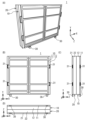
- FIG. 1A is a perspective view of the substrate housing case according to the first embodiment
- FIG. 1B is a diagram of the substrate housing case as seen from the +Z direction in FIG. 1(C) is a view of the board housing case viewed from the -X direction in FIG. 1(A)
- FIG. 1(D) is a view of the board housing case viewed from the -Y direction in FIG. 1(A).
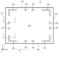
- FIG. 2 is a plan view of the lower box portion viewed from the +Z direction
- 3A is a cross-sectional view of the corner holder (a cross-sectional view taken along the line AA in FIG. 2), and FIG.
- FIG. 3B is a cross-sectional view of the side holder (a cross-sectional view taken along the line BB in cross-sectional view).
- FIG. 4 is a graph showing the measurement results of the dynamic friction coefficient of each test piece in the ball-on-disk test.
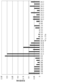
- FIG. 5 is a graph showing the measurement results of the wear scar depth of each test piece in the ball-on-disk test.
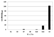
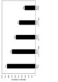
- FIG. 6 is a graph showing the total detected amount of Category 2 organic compound components for each sample.
- FIG. 7 is a graph showing the results of transportation tests.
- FIG. 8A is a cross-sectional view of the corner holder according to the second embodiment
- FIG. 8B is a cross-sectional view of the side holder according to the second embodiment.
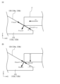
- FIG. 9A and 9B are cross-sectional views showing models used in the simulation.
- FIG. 11 is a graph showing the results of transportation tests.
- FIG. 12 is a cross-sectional view showing a side holder according to a modification.
- the mask/blank substrate While the mask/blank substrate is being stored in the substrate housing case and being transported, the mask/blank substrate undergoes minute reciprocating motion due to the vibrations that occur during transportation, resulting in a gap between the mask/blank substrate and the substrate holder. A phenomenon occurs that the substrate holder wears due to the friction generated in the . If a large amount of abrasion powder is generated due to abrasion of the surface of the substrate holder, fine dust may adhere to the surface of the mask/blank substrate.
- FIG. 1(A) is a perspective view of the substrate housing case 1 according to the first embodiment
- FIG. 1(B) is a diagram of the substrate housing case 1 viewed from the +Z direction in FIG. (C) is a view of the board housing case 1 viewed from the -X direction in FIG. 1 (A)
- FIG. 1 (D) is a view of the board housing case 1 viewed from the -Y direction in FIG. be.
- the shape, length, thickness, and other scales of each part shown in the embodiments do not necessarily match the actual thing, and in each drawing, some elements are omitted in order to facilitate understanding. may be
- the substrate housing case 1 is a case for housing a mask/blank substrate inside the case, protecting and transporting the housed mask/blank substrate.
- the size of the mask/blank substrate is, for example, 1220 ⁇ 1400 ⁇ 13 mm (diagonal dimension is about 1.8 m), and the mass is, for example, about 93 kg.
- the substrate housing case 1 includes an upper case unit 10 and a lower case unit 20.
- the substrate housing case 1 When housing the mask/blank substrate in the substrate housing case 1, the substrate housing case 1 is placed on the floor so that the bottom plate of the lower case unit 20 is parallel to the floor.
- direction or gravity direction Sometimes referred to as direction or gravity direction.
- the substrate storage case 1 shown in FIG. 1A is of a type in which the substrate storage case 1 is erected during transportation (so that the bottom plate of the lower case unit 20 is perpendicular to the floor surface) and the mask/blank substrate is transported.
- the substrate storage case 1 is of a type in which the mask/blank substrate is transported while the substrate storage case 1 is laid down (while the bottom plate of the lower case unit 20 is parallel to the floor surface) during transportation. There may be.
- the upper case unit 10 includes a metal upper frame 11 and a resin upper box portion 12 attached to the upper frame 11 .
- the lower case unit 20 also includes a metal lower frame 21 and a resin lower box portion 22 attached to the lower frame 21 .
- the upper box part 12 has a cover plate that covers the main surface of the mask/blank substrate and side walls that are connected to the side ends of the cover plate and extend downward, and is configured in a box shape that opens downward.
- Casters 30 for movement are attached to the upper frame 11 and the lower frame 21, respectively.
- a handle 31 used when moving the substrate housing case 1 is attached to the upper frame 11 and the lower frame 21 .
- FIG. 2 is a plan view of the lower box portion 22 viewed from the +Z direction.
- the lower box portion 22 has a bottom plate 22a that covers the main surface of the mask/blank substrate, and side walls 22b to 22e that are connected to side ends of the bottom plate 22a and extend upward. It has an open box shape.
- the mating surfaces of the lower end portion of the upper box portion 12 and the upper end portion of the lower box portion 22 are formed with a fitting structure that engages with each other to cover the upper case unit 10 from above.
- both are connected by bolts or the like, the mask/blank substrate housed inside the substrate housing case 1 is held in a sealed state.
- a substrate holder 23 for holding the edge of the mask/blank substrate in the thickness direction is provided inside the lower box portion 22 .
- the substrate holders 23 include L-shaped corner holders 23a provided at four locations to support corners of the mask/blank substrate, and center portions of each side of the mask/blank substrate. and a side retainer 23b provided.
- FIG. 3A is a cross-sectional view of the corner holder 23a (a cross-sectional view taken along line AA in FIG. 2)
- FIG. 3B is a cross-sectional view of the side holder 23b (B-B in FIG. B line sectional view). Note that the mask/blank substrate 2 is also shown in FIGS. 3A and 3B.
- the corner holder 23a includes a first member 23a1 and a second member 23a2.
- the first member 23 a 1 has a holding surface 24 a 1 that is in contact with the mask/blank substrate 2 and holds the mask/blank substrate 2 .
- the holding surface 24a1 holds the mask/blank substrate 2 from below.
- the holding surface 24a1 is subjected to one of dry cutting, wet cutting, and buffing.
- the mask/blank substrate 2 has a first main surface 2a, a second main surface 2b, a side surface 2c, a first connecting surface (first chamfered surface) 2d connecting the first main surface 2a and the side surface 2c, and a second connecting surface (second chamfered surface) 2e that connects the second main surface 2b and the side surface 2c.
- first major surface 2a is, for example, a patterned surface
- second main surface 2b may be a patterned surface or a patterned surface.
- the first main surface 2a and the second main surface 2b may be simply referred to as main surfaces 2a and 2b.
- the holding surface 24a1 includes a ridge portion (ridge line portion) r1 where the first connecting surface 2d of the mask/blank substrate 2 intersects with the first main surface 2a, and a ridge portion (ridge line portion) r1 where the side surface 2c and the first connecting surface 2d intersect. Of the ridge portion r2, it is in contact with the ridge portion r1.
- the holding surface (first holding surface) 24a1 is inclined with respect to a plane PL1 substantially parallel to the main surface (first main surface 2a) of the mask/blank substrate 2 held by the holding surface 24a1.
- the smaller angle ⁇ 1 is, for example, 3°.
- the angle ⁇ 1 may be referred to as the contact angle ⁇ 1 between the corner holder 23a and the mask/blank substrate 2.
- the contact angle ⁇ 1 is not limited to 3°, and may be less than 3° or greater than 3°.
- the plane PL1 is a plane that is substantially perpendicular or perpendicular to the direction of gravity.
- the second member 23a2 has the same shape as the first member 23a1, and is arranged line-symmetrically with respect to the center line CL1 in the thickness direction of the mask/blank substrate 2.
- the second member 23 a 2 has a holding surface 24 a 2 that is in contact with the mask/blank substrate 2 and holds the mask/blank substrate 2 .
- the holding surface 24a2 includes a ridge (ridge line) r3 where the second connecting surface 2e of the mask/blank substrate 2 intersects with the second main surface 2b, and a ridge (ridge) r3 where the side surface 2c and the second connecting surface 2e intersect. Of the ridge portion r4, it is in contact with the ridge portion r3.
- the holding surface (second holding surface) 24a2 is inclined with respect to a plane PL2 substantially parallel to the main surface (second main surface 2b) of the mask/blank substrate 2 held by the holding surface 24a2.
- the contact angle ⁇ 2 which is the smaller angle between the holding surface 24a2 and the plane PL2, may be the same as or different from the contact angle ⁇ 1.
- the holding surface 24a2 holds the mask/blank substrate 2 from above. Since other configurations of the second member 23a2 are the same as those of the first member 23a1, detailed description thereof will be omitted.
- the first member 23a1 and the second member 23a2 may be integrally formed or may be separate members. When the first member 23 a 1 and the second member 23 a 2 are separate members, the first member 23 a 1 is provided on the lower box portion 22 and the second member 23 a 2 is provided on the upper box portion 12 . Also, the first member 23a1 and the second member 23a2 may be in contact with each other in the Z direction, or may be separated from each other.
- the side holder 23b includes a first member 23b1 and a second member 23b2.
- the first member 23 b 1 has a holding surface (first holding surface) 24 b 1 that is in contact with the mask/blank substrate 2 and holds the mask/blank substrate 2 .
- first holding surface first holding surface
- the holding surface 24b1 holds the mask/blank substrate 2 from below.
- the holding surface 24b1 is subjected to one of dry cutting, wet cutting, and buffing.
- the holding surface 24b1 is in contact with the ridge r1 of the mask/blank substrate 2.
- the holding surface 24b1 is inclined with respect to a plane PL3 substantially parallel to the main surface (first main surface 2a) of the mask/blank substrate 2 held by the holding surface 24b1.
- the smaller angle ⁇ 3 is, for example, 3°.
- the angle ⁇ 3 may be referred to as a contact angle ⁇ 3 between the first member 23b1 of the side holder 23b and the mask/blank substrate 2.
- the contact angle ⁇ 3 is not limited to 3°, and may be less than 3° or greater than 3°.
- the second member 23b2 has a holding surface (second holding surface) 24b2 that holds the mask/blank substrate 2.
- the holding surface 24b2 holds the mask/blank substrate 2 from above.
- the holding surface 24b2 is subjected to one of dry cutting, wet cutting, and buffing.
- the holding surface 24b2 consists of a ridge r3 where the second connecting surface 2e of the mask/blank substrate 2 intersects with the second main surface 2b and a ridge r4 where the side surface 2c and the second connecting surface 2e intersect. , is in contact with the edge r3.
- the holding surface 24b2 is inclined with respect to a plane PL4 substantially parallel to the main surface (second main surface 2b) of the mask/blank substrate 2 held by the holding surface 24b2.
- the smaller angle ⁇ 4 is, for example, 3°.
- the angle ⁇ 4 may be referred to as a contact angle ⁇ 4 between the second member 23b2 of the side holder 23b and the mask/blank substrate 2.
- the contact angle ⁇ 4 is not limited to 3°, and may be less than 3° or greater than 3°. Further, the contact angle ⁇ 4 may be the same angle as the contact angle ⁇ 3, or may be a different angle. Note that when the substrate housing case 1 is placed on the floor such that the bottom plate 22a of the lower case unit 20 is parallel to the floor, the planes PL3 and PL4 are planes perpendicular to the direction of gravity.
- the second member 23b2 is a side of the mask/blank substrate 2 facing each other on a plane substantially parallel to the main surface (the first main surface 2a or the second main surface 2b) of the mask/blank substrate 2, as indicated by the arrow AR1. It is movable in a direction (X direction or Y direction) perpendicular to the . Thereby, the mask/blank substrate 2 can be reliably held by the substrate holder 23 .
- the first member 23b1 and the second member 23b2 are separate members in the first embodiment, they may be integrally formed.
- the entire side holder 23b is substantially the main surface (first main surface 2a or second main surface 2b) of the mask/blank substrate 2. In a parallel plane, it moves in a direction perpendicular to the side of the mask/blank substrate 2 facing it.
- the first member 23b1 and the second member 23b2 are separate members, the first member 23b1 is provided on the lower box portion 22 and the second member 23b2 is provided on the upper box portion 12 .
- the first member 23b1 and the second member 23b2 may be in contact with each other in the Z direction, or may be separated from each other.
- a tribological test was performed on a test piece made of the material with a size of 50 mm long, 50 mm wide, and 5 mm thick with a SiO2 glass ball having a diameter of 5 mm under a load of 800 g, a rotation speed of 50 rpm, and a measurement time of 1 hour. It is a material whose abrasion depth of the test piece after the abrasion is 6000 nm or less. Since the performance required for the mask/blank substrate holder is to generate as little wear powder as possible, a material with a small amount of wear, that is, a material with excellent wear resistance is suitable as a material for the substrate holder 23. be.
- the material of the substrate holder 23 is detected by a chromatography mass spectrometer among the outgases emitted while holding a test piece made of the material of 50 mm long ⁇ 50 mm wide ⁇ 5 mm thick at 100° C. for 300 minutes.
- the total amount of outgassed alkane compounds is 20 ⁇ g or less, preferably 5 ⁇ g or less. This is because it is desirable to avoid as much as possible alkane components with relatively high molecular weights from adhering to the surface of the mask blank.
- the alkane compound includes, for example, at least one of decane, undecane, dodecane, pentadecane, hexadecane, heptadecane, octadecane, nonadecane, eicosane, heneicosane, and docosane.
- ⁇ Tribology test> A tribology test was performed on a test piece (sometimes referred to as a sample) made of the material shown in Table 1 below and processed into a plate material of 50 mm long ⁇ 50 mm wide ⁇ 5 mm thick.
- sample E1 is PCTFE (polytrifluoroethylene chloride), and the surface is wet-milled.
- the material of sample E2 was PCTFE (polytrifluoroethylene chloride), and the surface was dry-milled.
- the material of sample E3 was a homopolymer POM (homopolymer polyacetal) Delrin® DRL-NA with a dry-milled surface.
- the material of sample E4 was Delrin (registered trademark) DRL-NA of homopolymer POM, and the surface was polished.
- the material of sample E5 was a copolymer POM (copolymer polyacetal) Duracon® M90-44, the surface of which was dry-milled.
- sample E6 was Duracon® NW-02, a copolymer POM, and the surface was dry-milled.
- the material of sample E7 was Duracon® NW-02LV of copolymer POM and the surface was dry-milled.
- the material of sample E8 is the Sepra standard of PI (polyimide), and the surface is dry-milled.
- the material of sample E9 is Sepra G1 of PI, and the surface is finished by buffing.
- the material of sample E10 is Sepra G2 of PI, and the surface is finished by buffing.
- the material of sample E11 is PI Vespel (registered trademark) SP-1, and the surface is buffed.
- the material of sample E12 is Vespel (registered trademark) SP-21 of PI, and the surface is finished by buffing.
- the material of sample E13 was PEEK (polyetheretherketone) PVX Black, and the surface was dry-milled.
- sample E14 is PVX Black of PEEK, and the surface is finished by polishing.
- the material of sample E15 is PEEK Ketron CA30, and the surface is dry-milled.
- the material of sample E16 is Ketron CA30 of PEEK, and the surface is finished by buffing.
- sample C1 is Polystone (registered trademark) M-sapphire of PE (polyethylene), and the surface is buffed.
- the material of sample C2 was PE Polystone® M-Sapphire and the surface was dry-milled.
- the material of sample C3 was a PE AS plate, and the surface was finished by polishing.
- the material of sample C4 was a PE AS plate, the surface of which was dry-milled.
- the material of sample C5 was PTFE (polytetrafluoroethylene), and the surface was wet-milled.
- the material of sample C6 was PTFE, and the surface was dry-milled.
- sample C7 is PTFE mixed with 15% glass and 5% molybdenum, and the surface is dry-milled.
- the material of sample C8 was PTFE containing 60% bronze, and the surface was dry-milled.
- the material of sample C9 is PTFE mixed with 10% carbon fiber, and the surface is dry-milled.
- the material of sample C10 is PTFE containing 15% carbon fiber, and the surface is dry-milled.
- the material of sample C11 is PTFE mixed with 15% carbon fiber, and the surface is wet-milled.
- the material of sample C12 was PTFE mixed with 15% graphite fiber, and the surface was dry-milled.
- the material of sample C13 is PTFE mixed with 30% graphite fiber, and the surface is wet-milled.
- sample C14 is PTFE containing 15% glass fiber, and the surface is dry-milled.
- the material of sample C15 is PTFE mixed with 15% glass fiber, and the surface is wet-milled.
- the material of sample C16 is PTFE containing 20% glass fiber, and the surface is dry-milled.
- the material of sample C17 is PTFE mixed with 20% glass fiber, and the surface is wet-milled.
- the material of sample C18 was PTFE containing 25% glass fiber, and the surface was dry-milled.
- PE and PTFE which are the materials of samples C1 to C6, are materials generally used for conventional substrate holders.
- Quartz (SiO 2 ) glass was selected as the material of the ball that was brought into contact with each test piece and made to rotate and slide. This is because, in actual operation, it is the mask/blank substrate made of quartz glass that comes into contact with the substrate holder.
- Fig. 4 shows the measurement results of the dynamic friction coefficient of each test piece.
- the vertical axis indicates the measured dynamic friction coefficient. It can be said that the smaller the dynamic friction coefficient, the lower the friction and the better the slidability of the material. Conversely, the larger the coefficient of dynamic friction, the more likely it is that dust will be generated by friction. There is a risk of damage.
- General sliding members are required to be designed so that the coefficient of dynamic friction is 0.1 or less. Therefore, it is preferable to use a material having a coefficient of dynamic friction of less than 0.1 as a candidate material for the substrate holder 23 .
- wear characteristics In the evaluation of wear characteristics, test pieces of each material were subjected to a ball-on-disk test under measurement conditions 2 below to form concentric wear marks on each test piece. After that, using a surface profiler (Tencor P-16+) manufactured by KLA (KLA Corporation), the depth, width and surface roughness of the wear scar were measured.
- Measurement condition 2 Ball: SiO2 glass ball with a diameter of 5 mm Rotation speed: 50 rpm Load: 800g Measurement time: 3600 seconds Temperature: 24°C Humidity: 40%
- Fig. 5 shows the measurement results of the depth of the wear scars of each test piece.
- the vertical axis represents the depth (nm) of the wear scar.
- a deeper wear scar indicates a greater amount of wear in the ball-on-disk test.
- the volume of material removed by abrasion falls off from the material as fine powder. That is, a large amount of wear means that a large amount of abrasion powder is generated. From FIG. 5, it can be seen that the amount of wear varies greatly depending on the material of the test piece.
- the performance required for the mask/blank substrate holder is to generate as little abrasion powder as possible, so a material with a small amount of abrasion, that is, a material with excellent abrasion resistance should be selected. Focusing on samples C5 to C18 made of PTFE-based materials, it can be seen that regardless of the presence or absence of additives, the wear scars are remarkably deep, the wear resistance is poor, and the amount of wear debris generated is large.
- the purpose of adding glass fiber, carbon fiber, and/or metal particles to PTFE as an additive is to improve mechanical strength, enhance slidability, impart electrical conductivity, and the like. However, the addition of glass fibers, carbon fibers, and/or metal particles did not improve the poor wear resistance properties.
- PCTFE, POM, PI, and PEEK are materials with excellent wear resistance. Further, a material with a small depth of wear marks is preferable for the substrate holder 23. Specifically, a material with a depth of wear marks of 4000 nm or less is more preferable, and a material with a depth of wear marks of 2000 nm or less is even more preferable. That is, it is determined that the samples E1 to E16 are appropriate materials for the substrate holder 23 from the measurement results of the wear characteristics shown in FIG.
- samples E1 to E8, E11, E12, and E14 to E16 are more suitable as materials for the substrate holder 23.
- VOC Volatile Organic Compounds
- PCTFE PCTFE
- sample E3 homopolymer POM Delrin (registered trademark) DRL-NA
- sample E7 copolymer POM Duracon (registered trademark) NW-02LV
- sample E8 Sepra standard on PI
- sample E10 Sepra G2 on PI
- sample E16 ketron CA30 on PEEK
- sample C3 AS plate on PE
- the sample surface was wiped with a wipe soaked with methanol and air-dried in a clean room for 4 hours. After that, the sample was heated with GL Sciences MD2580M-B, and the generated gas from the sample was collected in a TENAX tube (room temperature). The sample was heated from room temperature to 100° C. over 25 minutes and held at 100° C. for 300 minutes. The gas flow rate was 100 ml/min.
- Measurement was carried out by thermal desorption-gas chromatography/mass spectrometry (TD-GC/MS) method.
- TD-GC/MS thermal desorption-gas chromatography/mass spectrometry
- Collection tube desorption temperature 270°C GC introduction method: After cold trapping at -130°C, heating at 270°C
- Carrier gas He Ionization method: EI method GC temperature elevation conditions: 40°C (held for 5 minutes) ⁇ 10°C/min temperature rise ⁇ 280°C (held for 21 minutes)
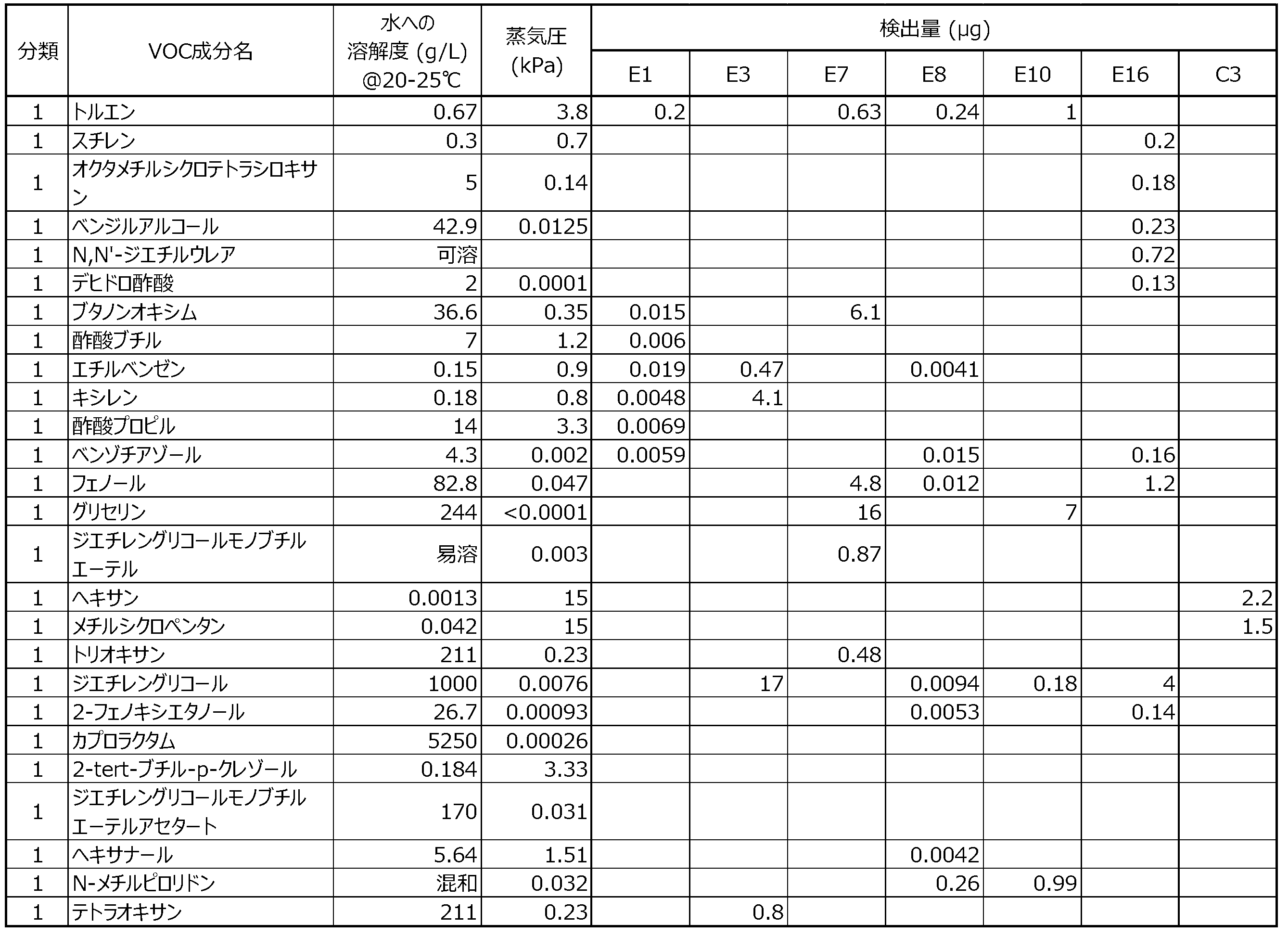
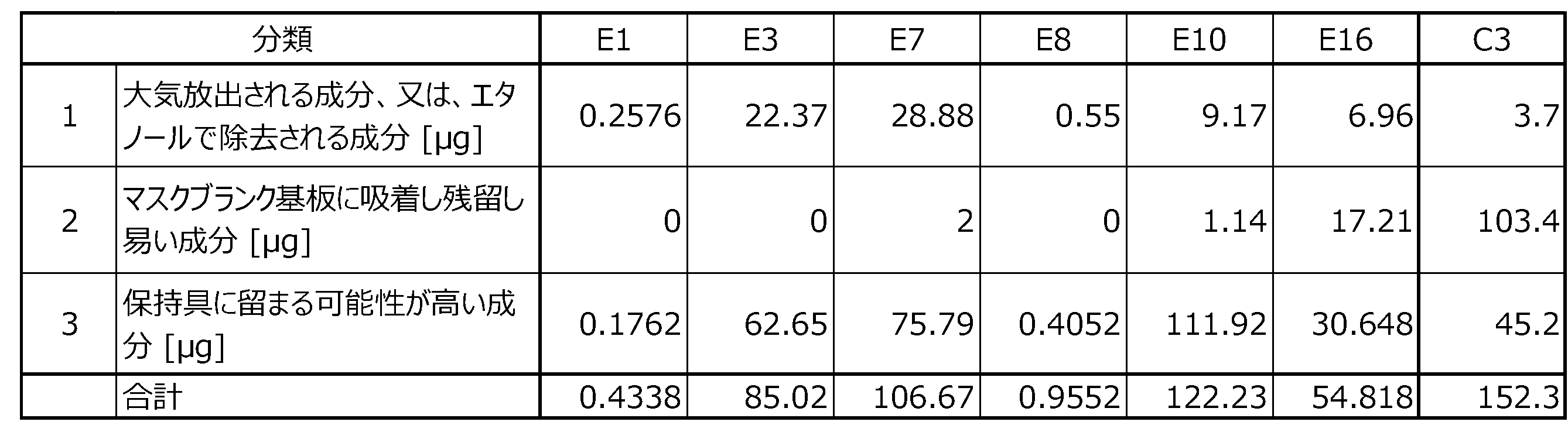
- Organic compound components of category 1 are organic compound components that are released into the atmosphere due to their high volatility, or are removed with ethanol due to their high solubility in water and ethanol. Examples include toluene, styrene, octamethylcyclotetrasiloxane, benzyl alcohol, N,N'-diethylurea, dehydroacetic acid, butanone oxime, butyl acetate, ethylbenzene, xylene, propyl acetate, benzothiazole, phenol, glycerin, diethylene glycol monobutyl ether.
- hexane methylcyclopentane, trioxane
- diethylene glycol 2-phenoxyethanol
- caprolactam 2-tert-butyl-p-cresol
- diethylene glycol monobutyl ether acetate hexanal
- N-methylpyrrolidone and tetraoxane.
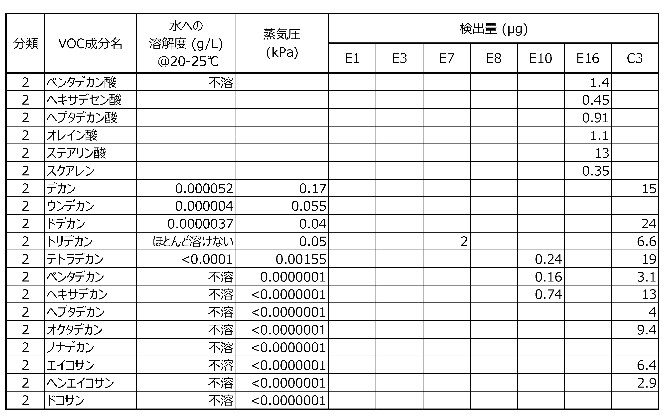
- the organic compound components of Class 2 are organic compound components that are likely to be adsorbed to and remain on the mask/blank substrate. , undecane, dodecane, tridecane, tetradecane, pentadecane, hexadecane, heptadecane, octadecane, nonadecane, eicosane, heneicosane, and docosane.
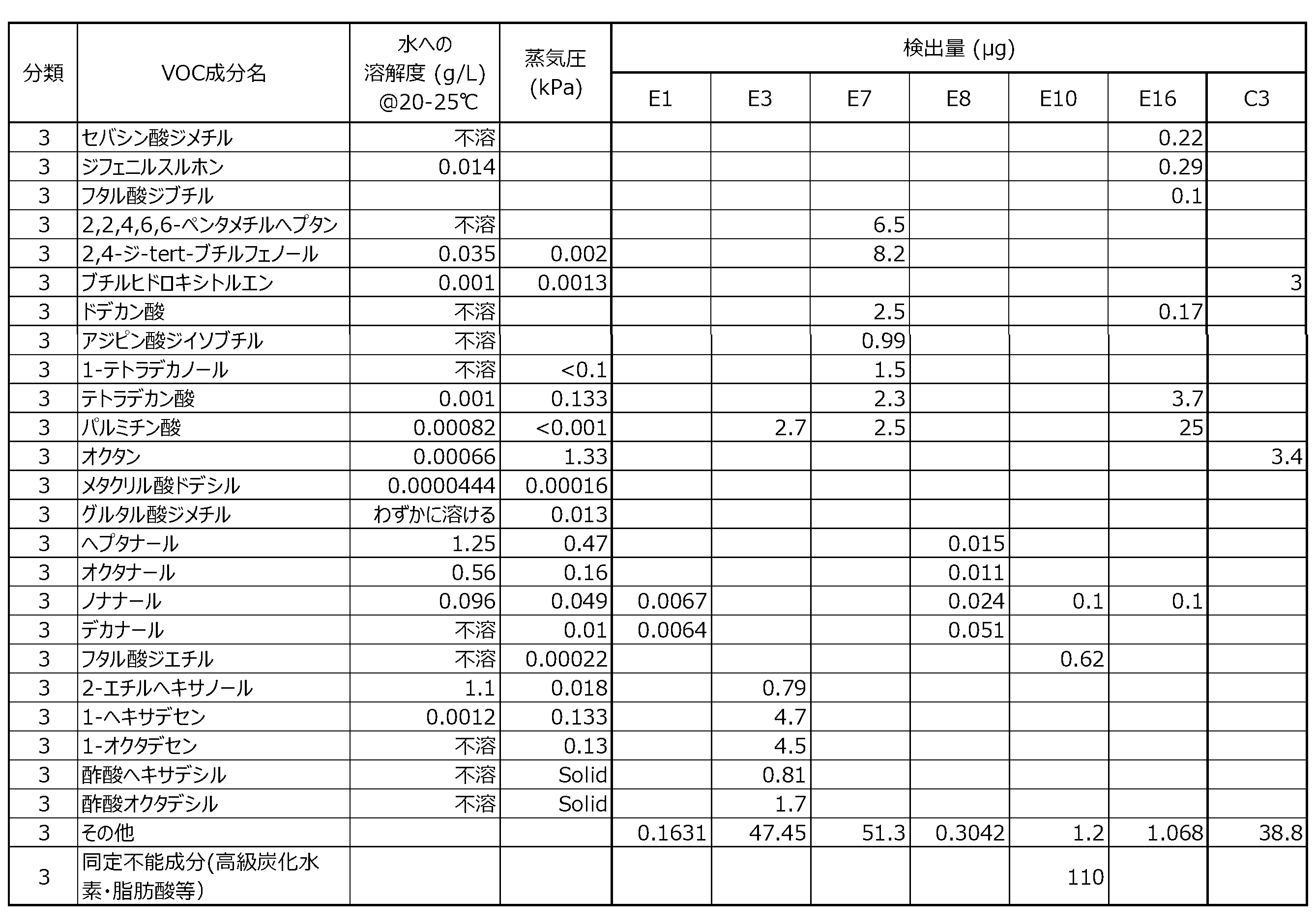
- Category 3 organic compound components have a low vapor pressure and are sparingly soluble in water and ethanol, so they are highly likely to remain in the substrate holder.
- Tables 2 to 4 show the detected amount of each organic compound component of categories 1 to 3, respectively, and Table 5 shows the total detected amount of the organic compound component of categories 1 to 3.
- FIG. 6 is a graph showing the total detected amount of organic compound components of Category 2 for each sample.
- PCTFE Sample E1
- PI Sepra standard Sample E8
- the total amount of VOCs detected is correspondingly large.
- Category 1 is an organic compound component that is released into the atmosphere due to its high volatility, or is easily dissolved in water and ethanol and is removed with ethanol. / It is considered that the possibility of adversely affecting the quality of the blank substrate is low. Further, the total amount of detected alkane components is preferably 20 ⁇ g or less. Furthermore, it is preferable that the total amount of alkane components to be detected is as small as possible.
- the PE AS plate (Sample C3) has a total of 103.4 ⁇ g of alkane components with relatively large molecular weights, which is an overwhelmingly high value compared to test pieces made of other materials.
- the alkane components actually detected were decane 15 ⁇ g, dodecane 24 ⁇ g, tridecane 6.6 ⁇ g, tetradecane 19 ⁇ g, pentadecane 3.1 ⁇ g, hexadecane 13 ⁇ g, heptadecane 4 ⁇ g, octadecane 9.4 ⁇ g, eicosane 6.4 ⁇ g, and heneicosane 2.9 ⁇ g. there were.
- alkane component having a relatively large molecular weight is volatilized and released into the substrate housing case 1 from the substrate holder 23 attached in the lower box portion 22 of the substrate housing case 1, and is adsorbed on the surface of the mask blank, causing a serious problem. may occur.
- these alkane components with relatively large molecular weights adhere to the mask blank, they remain in a state of being adhered for a long period of time because they are difficult to revolatilize from the mask blank due to their low vapor pressure. Since the alkane component is a non-polar lipophilic component, wettability of the resist is significantly different between a region on the mask blank where the alkane component adheres and a region where the alkane component does not adhere. Therefore, when the resist is applied, unevenness occurs, and after exposure, development, and wet etching processes, a photomask having a pattern structure as designed cannot be finished.
- PCTFE and PI are particularly excellent candidates for replacing PTFE, which is generally used in conventional substrate holders, and PI (Sepra G2), Homopolymer POM (Delrin (registered trademark) DRL-NA), copolymer POM (Duracon (registered trademark) NW-02), and PEEK (ketron CA30) are also considered satisfactory.
- Ethanol resistance was evaluated as the chemical resistance of each sample.
- the reason why ethanol is used is that ethanol is normally used when cleaning the dedicated storage case and parts such as substrate holders provided in the case.
- a wiping cloth impregnated with 99.5% industrial ethyl alcohol was used to rub the surface of the test piece 10 times at a speed of 1 second per reciprocation, and then the appearance of each test piece was visually observed. .
- the materials of the substrate holder 23 are polytrifluoroethylene chloride (PCTFE), polyimide (PI), and polyacetal (POM). , and polyetheretherketone (PEEK).
- the substrate holder 23 is provided in the substrate housing case 1 that houses the mask/blank substrate 2 , and serves as a substrate holder for holding the mask/blank substrate 2 .
- the material of the substrate holder 23 is a tribology test with a load of 800 g, a rotation speed of 50 rpm, and a measurement time of 1 hour with a SiO 2 glass ball of 5 mm in diameter against a test piece of 50 mm in length ⁇ 50 mm in width ⁇ 5 mm in thickness. It is a material whose wear depth of the test piece after performing is 6000 nm or less. As a result, it is possible to suppress the generation of abrasion powder.
- the material of the substrate holder 23 is selected from the outgassed out gas emitted while a test piece of 50 mm long ⁇ 50 mm wide ⁇ 5 mm thick is held at 100° C. for 300 minutes.
- the total amount of outgassing of alkane compounds detected in total is 20 ⁇ g or less. This makes it possible to prevent the alkane component having a relatively large molecular weight from adhering to the surface of the mask blank as much as possible.
- the substrate holder 23 is provided in the substrate housing case 1 for housing the mask/blank substrate 2, and is a substrate holder for holding the mask/blank substrate 2.
- the material of the fitting 23 is either polytrifluoroethylene (PCTFE), polyimide (PI), polyacetal (POM), or polyetheretherketone (PEEK). As a result, it is possible to suppress the generation of abrasion powder.
- Example 2 A mask/blank substrate was actually transported using the substrate housing case equipped with the substrate holder according to the first embodiment, and the amount of dust detected from the mask/blank substrate was confirmed.
- an inner case (model number BXAL-12141SSN8-N, equivalent to substrate storage case 1) made of polyacrylonitrile (PAN, Barex) material made by Net Plastic Co., Ltd. and the inner case was used.
- PAN polyacrylonitrile
- a transportation test was performed as follows.
- the G8 size quartz glass substrate was stored in the inner case.
- the glass substrate is in a state of being supported by the substrate holder.
- the inner case containing the glass substrate was stored in the outer case and loaded on the bed of the truck. In a state in which the outer case was prevented from overturning, it was transported on a public road in the process of Nikon Corporation Sagamihara Manufacturing Co., Ltd. ⁇ Nikon Corporation Shonan Branch Office ⁇ Nikon Corporation Sagamihara Manufacturing Co., Ltd.
- Example 1 the material of the substrate holder 23 is homopolymer POM (Delrin (registered trademark) DRL-NA), in Example 2, the material of the substrate holder 23 is PI (Sepra standard), and in Example 3, the substrate The material of the holder 23 is a copolymer POM (Duracon (registered trademark) NW-02), and in Example 4, the material of the substrate holder 23 is PCTFE.
- the contact angles .theta.1 and .theta.2 at the corner holder 23a and the contact angles .theta.3 and .theta.4 at the side holder 23b were set to 3.degree.
- Comparative Example 1 was a PTFE holder.
- the contact angles ⁇ 1, ⁇ 2, ⁇ 3 and ⁇ 4 were 3°.
- Figure 7 shows the results of the transport test.
- the vertical axis represents the amount of increase in dust having a size of ⁇ 0.3 ⁇ m or more.
- PCTFE polytrifluoroethylene
- PI polyimide
- POM polyacetal
- PEEK polyetheretherketone
- FIG. 8A is a sectional view of a corner holder 123a according to the second embodiment
- FIG. 8B is a sectional view of a side holder 123b according to the second embodiment.
- the corner holder 123a corresponds to the corner holder 23a in the first embodiment
- the side holder 123b corresponds to the side holder 23b in the first embodiment.
- the holding surface (first holding surface) 124a1 is a plane substantially parallel to the main surface (first main surface 2a) of the mask/blank substrate 2 held by the holding surface 124a1. It is inclined with respect to PL11, and the contact angle ⁇ 11, which is the smaller angle between the holding surface 124a1 and the plane PL11, is set to an angle of 4° or more and 45° or less.
- the holding surface (second holding surface) 124a2 is the main part of the mask/blank substrate 2 held by the holding surface 124a2.
- the contact angle ⁇ 12 which is the smaller angle between the holding surface 124a2 and the plane PL12, is also 4° or more and 45° or less. It's becoming
- a holding surface (first holding surface) 124b1 is inclined with respect to a plane PL13 substantially parallel to the main surface (first main surface 2a) of the mask/blank substrate 2, and is held with the plane PL13.
- a contact angle ⁇ 13 which is the smaller one of the angles formed with the surface 124b1, is set to an angle of 4° or more and 45° or less.
- the holding surface (second holding surface) 124b2 is inclined with respect to the plane PL14 substantially parallel to the main surface (second main surface 2b) of the mask/blank substrate 2, and the plane PL14 and the holding surface 124b2 form.
- a contact angle ⁇ 14 which is the smaller one of the angles, is set to an angle of 4° or more and 45° or less.
- FIGS. 9A and 9B are cross-sectional views showing models used in the simulation. In FIGS. 9A and 9B, hatching indicating a cross section is omitted.
- the holding surfaces 124a1 and 124a2 are collectively referred to as a holding surface 124a
- the holding surfaces 124b1 and 124b2 are collectively referred to as a holding surface 124b.
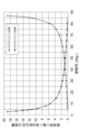
- an index that relatively indicates the stress generated in the substrate holder 123 can be expressed as (1/tan ⁇ ) ⁇ aE/t.
- ⁇ represents the coefficient of dynamic friction
- E represents the modulus of longitudinal elasticity of the material of the substrate holder 123
- a represents the long side of the contact surface between the mask/blank substrate 2 and the substrate holder 123
- t represents the thickness of the substrate holder 123 .
- FIG. 9B consider a case where the mask/blank substrate 2 is slightly moved in the Z direction due to vibrations during transportation and pressed against the substrate holder 123 .
- an index that relatively indicates the stress generated in the substrate holder 123 can be expressed as (tan ⁇ ) ⁇ aE/t.
- the horizontal axis indicates the contact angle ⁇
- the stress associated with displacement in the X direction is the largest, but the stress associated with displacement in the Z direction is the smallest.
- the contact angle ⁇ is set to 60° or less. Further, when the mask/blank substrate 2 is supported by the substrate holder 123, it is necessary to consider the play dimension, so the contact angle ⁇ is preferably 45° or less. Therefore, in the second embodiment, in order to support the mask/blank substrate 2 with good working efficiency while reducing the amount of abrasion powder generated from the substrate holder, the contact angle ⁇ is set within the range of 4° to 45°. angle. From the viewpoint of reducing the amount of abrasion powder generated, the lower limit of the contact angle ⁇ is more preferably 10°, still more preferably 20°.
- the corner holders 123a and the side holders 123b are provided in the substrate housing case 1 that houses the mask/blank substrate 2, and the mask/blank substrate 2, corner holders 123a and side holders 123b have holding surfaces 124a1 and 124b1, respectively, which hold the mask/blank substrate 2 in contact therewith. Furthermore, the smaller angles ⁇ 11 and ⁇ 12 of the angles formed by the holding surfaces 124a1 and 124b1 and the planes PL11 and PL12 substantially parallel to the main surface 2a or 2b of the mask/blank substrate 2 held by the holding surfaces 124a1 and 124b1, respectively. is 4° or more and 45° or less. As a result, the stress generated in the corner holder 123a and the side holder 123b can be kept within a range in which the amount of abrasion powder generated can be suppressed. can reduce the amount of abrasion powder generated.
- the first member 123b1 and the second member 123b2 of the side holder 123b may be separate or integrally formed.
- the entire side holder 123b is substantially the main surface (first main surface 2a or second main surface 2b) of the mask/blank substrate 2. In a parallel plane, it moves in a direction (X direction or Y direction) perpendicular to the sides of the mask/blank substrate 2 facing each other.
- the first member 123b1 and the second member 123b2 may be in contact with each other in the Z direction, or may be separated from each other.
- Example 2 Substrate holders 123 with different contact angles ⁇ were manufactured, and a mask/blank substrate was actually transported using a substrate housing case equipped with the manufactured substrate holders 123, and the amount of dust detected on the mask/blank substrate. It was confirmed.
- the inner case and outer case used in the transportation test are the same as those of Examples 1 to 4 and Comparative Example 1.
- the transportation test implementation method and evaluation method are the same as in Examples 1 to 4 and Comparative Example 1.
- Example 5 In Example 5, the material of the substrate holder 123 is PTFE, the contact angle ⁇ 11 of the corner holder 123a is 5°, the contact angle ⁇ 12 is 17.5°, and the contact angle ⁇ 13 of the side holder 123b is 5°. , the contact angle ⁇ 14 was 17.5°.
- Example 6 the material of the substrate holder 123 is PTFE, the contact angle ⁇ 11 of the corner holder 123a is 12.5°, the contact angle ⁇ 12 is 17.5°, and the contact angle ⁇ 13 of the side holder 123b is 12.5°, and the contact angle ⁇ 14 was 17.5°.
- Example 7 the material of the substrate holder 123 is PCTFE, and the contact angles ⁇ 11 and ⁇ 12 of the corner holder 123a and the contact angles ⁇ 13 and ⁇ 14 of the side holder 123b are 3°.
- Example 8 the material of the substrate holder 123 is PCTFE, the contact angle ⁇ 11 of the corner holder 123a is 5°, the contact angle ⁇ 12 is 17.5°, and the contact angle ⁇ 13 of the side holder 123b is 5°. , the contact angle ⁇ 14 was 17.5°.
- Example 9 the material of the substrate holder 123 is PCTFE, the contact angle ⁇ 11 of the corner holder 123a is 12.5°, the contact angle ⁇ 12 is 17.5°, and the contact angle ⁇ 13 of the side holder 123b is 12°. .5 and ⁇ 14 were set to 17.5°.
- Example 10 the material of the substrate holder 123 is PCTFE, and the contact angles ⁇ 11 and ⁇ 12 of the corner holder 123a and the contact angles ⁇ 13 and ⁇ 14 of the side holder 123b are 45°.
- Comparative example 2 As Comparative Example 2, a substrate holder made of PTFE and having a contact angle of 3° between the holding surface of the substrate holder and the mask/blank substrate was prepared.
- Fig. 11 shows the results of the transportation test.
- the vertical axis represents the amount of increase in dust having a size of ⁇ 0.3 ⁇ m or more.
- the contact angle between the substrate holder and the mask/blank substrate is set to 4° or more.
- the reason why the contact angle is preferably 4° or more is as follows.
- the stress index which is the vertical axis in FIG. 10, is directly related to the amount of dust generated by transportation. From the results of FIG. 10, when the contact angle is between 3° and 10°, the stress index in the Z direction does not change substantially, but the stress index in the X direction changes greatly. It can be seen that the stress index is dominant and has a large effect on dust generation. That is, when the contact angle is between 3° and 10°, the stress index in the X direction is proportional to the amount of dust.
- Table 6 shows the results of summarizing changes in the stress index for each 1° from 3° to 10°. Table 6 also shows that the stress index changes sharply from 3° to 4°. From the results of FIG. 10 and Table 6, the amount of dust increased at a contact angle of 3° (8535) and the amount of dust increased at a contact angle of 5° (3587), and the amount of dust increased at a contact angle of 4° was about 5450. Since the amount of increased dust is less than 6000, it is considered that the increased amount of dust can be suppressed even when the contact angle is 4°. Therefore, the contact angle is preferably 4° or more.
- the substrate holder made of PCTFE which is considered to be suitable as a material for the substrate holder, has a contact angle of 5° or 12.5°. It can be seen that the amount of dust increase after the transportation test is also reduced.
- the larger the contact angle the smaller the stress, so it is expected that the larger the contact angle, the smaller the dust increase amount. That is, when the contact angle is 45°, the amount of dust increase is expected to be the smallest.
- the substrate holder with a contact angle of 45° has a large dust increase as shown in FIG. This is considered to be due to the following reasons.
- the contact angle ⁇ 11 between the holding surface 124a1 and the mask/blank substrate 2 in the corner holder 123a is preferably 4° or more and 20° or less.
- the contact angle ⁇ 12 between the holding surface 124a2 and the mask/blank substrate 2 is preferably 4° or more and 20° or less.
- the lower limit of the contact angles ⁇ 11 and ⁇ 12 is more preferably 4.5°, still more preferably 5°, in order to suppress the increase in dust.
- the upper limit of the contact angles ⁇ 11 and ⁇ 12 is more preferably 15°, still more preferably 13°.
- the contact angle ⁇ 13 between the holding surface 124b1 and the mask/blank substrate 2 in the side holder 123b is preferably 4° or more and 20° or less.
- the contact angle ⁇ 14 between the holding surface 124b2 and the mask/blank substrate 2 is preferably 4° or more and 20° or less.
- the lower limit of the contact angles ⁇ 13 and ⁇ 14 is 4.5°, more preferably 5°, in order to suppress the increase in dust.
- the upper limit of the contact angles ⁇ 13 and ⁇ 14 is more preferably 15°, still more preferably 13°.
- the lower limit of the contact angles ⁇ 11 and ⁇ 12 of the corner holder 123a is preferably 10° or more, more preferably 20° or more.
- the lower limit of the contact angles ⁇ 13 and ⁇ 14 of the side holder 123b is preferably 10° or more, more preferably 20° or more.
- the contact angles ⁇ 11 to ⁇ 14 of the substrate holder 123 should be 45° to suppress the increase in dust, according to the simulation results of FIG. ° or more and 80° or less.
- the upper limit of the contact angles ⁇ 11 to ⁇ 14 may be 80° or less, more preferably 70° or less, and even more preferably 60° or less.
- FIG. 12 is a cross-sectional view showing a side holder 223b according to a modification. In FIG. 12, hatching indicating a cross section is omitted.
- the ridge r3 of the second connecting surface 2e and the holding surface of the second member come into contact with each other.
- the holding surface of the second member 223b2 of the side holder 223b (Second holding surface) 224b2 contacts the lower ridge r4 of the two ridges r3 and r4 of the second connection surface 2e.
- the smaller angle ⁇ 22 is 50° or more and 70° or less. is the angle of
- the holding surface 224b2 can be brought into contact with the ridge r4, and even if dust is generated from the side holder 223b, adhesion of abrasion powder to the main surface 2b of the mask/blank substrate 2 can be suppressed. can. Also, the mask/blank substrate 2 can be reliably held.
- the contact angle ⁇ 22 is preferably 60° or more and 70° or less.
- the first member 223b1 and the second member 223b2 of the side holder 223b may be separate or integrally formed.
- the entire side holder 223b is substantially the main surface (first main surface 2a or second main surface 2b) of the mask/blank substrate 2. In a parallel plane, it moves in a direction (X direction or Y direction) perpendicular to the sides of the mask/blank substrate 2 facing each other.
- the first member 223b1 and the second member 223b2 may be in contact with each other in the Z direction, or may be separated from each other.
Landscapes
- Physics & Mathematics (AREA)
- General Physics & Mathematics (AREA)
- Container, Conveyance, Adherence, Positioning, Of Wafer (AREA)
- Details Of Rigid Or Semi-Rigid Containers (AREA)
- Packaging Of Annular Or Rod-Shaped Articles, Wearing Apparel, Cassettes, Or The Like (AREA)
Abstract
Description
以下、第1実施形態に係る基板収容ケースについて図面を参照して説明する。図1(A)は、第1実施形態に係る基板収容ケース1の斜視図であり、図1(B)は、基板収容ケース1を図1(A)において+Z方向から見た図、図1(C)は、基板収容ケース1を図1(A)において-X方向から見た図、図1(D)は、基板収容ケース1を図1(A)において-Y方向から見た図である。なお、実施形態に示す各部の形状や、長さ、厚みなどの縮尺は必ずしも実物と一致するものではなく、また、各図において、理解を容易にするため、一部の要素の図示を省略している場合がある。
基板収容ケース1は、マスク/ブランク基板をケース内部に収容し、収容されたマスク/ブランク基板を保護し運搬するためのケースである。
基板保持具23の材料は、縦50mm×横50mm×厚み5mmの当該材料からなる試験片に対して直径5mmのSiO2ガラス球で荷重800g、回転数50rpm、計測時間1時間のトライボロジー試験を行った後の試験片の摩耗深さが6000nm以下である材料である。マスク/ブランク基板向け保持具に求められる性能は摩耗粉の発生量が極力少ないことであるから、摩耗量の少ない材質すなわち耐摩耗性に優れた材質が、基板保持具23の材料として適切だからである。
縦50mm×横50mm×厚み5mmの板材に加工した、下記の表1に示す材質からなる試験片(サンプルと記載する場合がある)についてトライボロジー試験を行った。

上記サンプルの摩擦特性及び摩耗特性を評価するため、ボールオンディスク試験を行った。ボールオンディスク試験は、株式会社レスカ(RHESCA Co., LTD.)製の摩擦摩耗試験機(フリクションプレーヤ:FPR-2100)を用いて実施した。
摩擦特性の評価では、以下の測定条件1にて、各材質の試験片に対してボールオンディスク試験を実施し、各試験片の動摩擦係数を評価した。
測定条件1:
ボール:直径10mmのSiO2ガラス球
回転数:50rpm
荷重:50g
計測時間:3600秒
温度:24℃
湿度:40%
摩耗特性の評価では、以下の測定条件2にて、各材質の試験片に対してボールオンディスク試験を実施し、各試験片に同心円状の摩耗痕を形成した。その後、KLA(KLA Corporation)製の表面プロファイラ(stylus profiler:Tencor P-16+)を用いて、摩耗痕の深さ、幅、表面粗さを計測した。
測定条件2:
ボール:直径5mmのSiO2ガラス球
回転数:50rpm
荷重:800g
計測時間:3600秒
温度:24℃
湿度:40%
表1のサンプルの中から、サンプルE1(PCTFE),サンプルE3(ホモポリマーPOMのデルリン(登録商標)DRL-NA)、サンプルE7(コポリマーPOMのジュラコン(登録商標)NW-02LV)、サンプルE8(PIのセプラ標準)、サンプルE10(PIのセプラG2)、サンプルE16(PEEKのketron CA30)、およびサンプルC3(PEのASプレート)について、VOC放出特性を評価した。
ベーキング済みのステンレス製密閉容器内に縦50mm×横50mm×厚み5mmの試験片を格納して、ガス捕集管(TENAX-GR)を用いて該ステンレス容器内の雰囲気ガスを吸着捕集した。次に、ガス捕集管を加熱して吸着ガス成分を脱着させて、脱着ガス成分をGC/MS(Gas Chromatography Mass Spectrometry)分析装置内へ導入し、有機成分の定性分析および定量分析を行った。実際の測定方法を下記に示す。
試料表面をメタノールのついたワイプで拭き、クリーンルーム内で4時間風乾した。その後、試料をジーエルサイエンス MD2580M-Bにて加熱し、サンプルからの発生ガスをTENAX管(室温)に回収した。試料は、室温から100℃まで25分かけて昇温させ、100℃を300分保持した。ガス流量は、100ml/minとした。
加熱脱着-ガスクロマトグラフ/質量分析(TD-GC/MS)法により測定を行った。加熱脱離装置としてジーエルサイエンス TD2530を使用し、ガスクロマトグラフとしてAgilent Technologies 7890B GC Systemを使用し、質量分析検出器としてAgilent Technologies 5977A MSDを使用した。
捕集管脱着温度:270℃
GC導入法:-130℃でコールドトラップ後、270℃で加熱
カラム:InertCap 1MS(Length:60m, Diam:0.25mm, Film:0.25μm)
キャリアガス:He
イオン化法:EI法
GC昇温条件:40℃(5分間保持)→10℃/min昇温→280℃(21分間保持)
各サンプルの耐薬品性として、エタノール耐性を評価した。エタノールを用いる理由は、専用収納ケースおよびケース内に具備された基板保持具等の部品を清掃する際には、通常、エタノールを用いているからである。試験方法としては、工業用エチルアルコール99.5%を染み込ませた拭き布を用いて、1往復当り1秒間の速度で試験片の表面を10往復擦った後、各試験片の外観を目視した。
第1実施形態に係る基板保持具を装着した基板収容ケースを用いて、実際にマスク/ブランク基板を運搬し、マスク/ブランク基板上から検出される粉塵量を確認した。
実施例1では、基板保持具23の材質をホモポリマーPOM(デルリン(登録商標)DRL-NA)とし、実施例2では基板保持具23の材質をPI(セプラ標準)とし、実施例3では基板保持具23の材質をコポリマーPOM(ジュラコン(登録商標)NW-02)とし、実施例4では基板保持具23の材質をPCTFEとした。角部保持具23aにおける接触角θ1及びθ2および辺部保持具23bにおける接触角θ3及びθ4は、実施例1~実施例4のいずれにおいても3°とした。
比較例1は、PTFE製保持具とした。接触角θ1、θ2、θ3及びθ4は、3°であった。
レーザーテック(株)製の大型マスクブランクス欠陥検査装置LBIS(型番L1052)を用いて、運搬試験の直前および直後の石英ガラス基板上にて検出される全粉塵数を計数して、その差分を算出した。LBISの分解能は0.3μmであることから、Φ0.3μm以上のサイズからなる粉塵の全数を計数した。
図8(A)は、第2実施形態に係る角部保持具123aの断面図であり、図8(B)は、第2実施形態に係る辺部保持具123bの断面図である。角部保持具123aは、第1実施形態における角部保持具23aに対応し、辺部保持具123bは、第1実施形態における辺部保持具23bに対応する。
接触角θが異なる基板保持具123を作製し、作製した基板保持具123を装着した基板収容ケースを用いて、実際にマスク/ブランク基板を運搬し、マスク/ブランク基板上から検出される粉塵量を確認した。運搬試験に用いるインナーケース及びアウターケースは、実施例1~4および比較例1と同様である。また、運搬試験の実施方法及び評価方法は、実施例1~4および比較例1と同様である。
実施例5では、基板保持具123の材質をPTFEとし、角部保持具123aの接触角θ11を5°、接触角θ12を17.5°、並びに辺部保持具123bの接触角θ13を5°、接触角θ14を17.5°とした。実施例6では、基板保持具123の材質をPTFEとし、角部保持具123aの接触角θ11を12.5°、接触角θ12を17.5°、並びに辺部保持具123bの接触角θ13を12.5°、接触角θ14を17.5°とした。
比較例2として、材質がPTFEであり、基板保持具の保持面とマスク/ブランク基板とがなす接触角が3°である基板保持具を準備した。

第1実施形態及び第2実施形態において、辺部保持具23b及び123bの形状をさらに変更してもよい。図12は、変形例に係る辺部保持具223bを示す断面図である。図12では、断面を示すハッチングを省略している。
2 マスク/ブランク基板
23,123 基板保持具
23a,123a 角部保持具
23a1,123a1 第1部材
23a2,123a2 第2部材
23b,123b,223b 辺部保持具
23b1,123b1,223b1 第1部材
23b2,123b2,223b2 第2部材
24a1,124a1 保持面(第1保持面)
24a2,124a2 保持面(第2保持面)
24b1,124b1,224b1 保持面(第1保持面)
24b2,124b2,224b2 保持面(第2保持面)
Claims (25)
- 1つの側面に2つの面取り面を有する基板を収容する基板収容ケースに備えられ、前記基板と接触して前記基板を保持する基板保持具であって、
前記基板保持具は、前記2つの面取り面のうち第1面取り面の一部と接触して前記基板を保持する第1保持面と、前記2つの面取り面のうち第2面取り面の一部と接触して前記基板を保持する第2保持面と、を有し、前記第1保持面を、前記第1面取り面が有する2つの稜線部のうち、1つの稜線部と接触させ、前記第2保持面を、前記第2面取り面が有する2つの稜線部のうち、1つの稜線部と接触させて、前記基板を保持する基板保持具。 - 前記基板保持具は、前記基板を載置したとき、前記第1面取り面が有する2つの稜線部のうち下方の稜線部を前記第1保持面によって保持させ、前記第2面取り面が有する2つの稜線部のうち、上方の稜線部を前記第2保持面によって保持させる、
請求項1に記載の基板保持具。 - 前記第1保持面と、重力方向に直交する水平面とのなす角度のうち小さい方の角度である第1角度は、4°以上45°以下である、
請求項1または2に記載の基板保持具。 - 前記第2保持面と前記水平面とのなす角度のうち小さい方の角度である第2角度は、4°以上45°以下である、
請求項3に記載の基板保持具。 - 前記第1角度及び前記第2角度は、4°以上20°以下である、
請求項4に記載の基板保持具。 - 前記基板保持具は、前記基板を載置したとき、前記第1面取り面が有する2つの稜線部のうち下方の稜線部を前記第1保持面によって保持させ、前記第2面取り面が有する2つの稜線部のうち、下方の稜線部を前記第2保持面によって保持させる、
請求項2に記載の基板保持具。 - 前記第1保持面と重力方向に直交する水平面とのなす角度のうち小さい方の角度である第1角度は、4°以上45°以下である、
請求項6に記載の基板保持具。 - 前記第2保持面と前記水平面とのなす角度のうち小さい方の角度である第2角度は、前記第1角度よりも大きい、
請求項7に記載の基板保持具。 - 前記第2保持面と重力方向に直交する水平面とのなす角度のうち小さい方の角度である第2角度は、50°以上70°以下である、
請求項6から請求項8のいずれか一項に記載の基板保持具。 - 前記第2角度は、60°以上70°以下である、
請求項9に記載の基板保持具。 - 前記第1保持面及び前記第2保持面は、ドライ切削加工、ウェット切削加工、およびバフ研磨加工のいずれかの加工がされている、
請求項1から請求項10のいずれか1項に記載の基板保持具。 - 基板を収容する基板収容ケースに備えられ、前記基板と接触して前記基板を保持する基板保持具であって、
前記基板保持具は、前記基板の一部と接触して前記基板を保持する保持面と、 前記基板と接触する前記保持面の材料は、ポリ三フッ化塩化エチレン(PCTFE)、ポリイミド(PI)、およびポリエーテルエーテルケトン(PEEK)のいずれかである、基板保持具。 - 前記基板保持具は、前記基板の角部を保持し、または、前記基板の周辺部の一部を保持する、請求項1から請求項12のいずれか一項に記載の基板保持具。
- 基板を収容する基板収容ケースに備えられ、前記基板と接触して前記基板を保持する基板保持具であって、
前記基板保持具は、前記基板の一部と接触して前記基板を保持する保持面を有し、
前記保持面の材料は、縦50mm×横50mm×厚さ5mmの前記材料からなる試験片に対して直径5mmのSiO2ガラス球で荷重800g、回転数50rpm、計測時間1時間のトライボロジー試験を行った後の前記材料からなる試験片の摩耗深さが6000nm以下である材料であり、ポリアセタール(POM)を含まない、
基板保持具。 - 前記保持面の材料は、縦50mm×横50mm×厚さ5mmの前記材料からなる試験片を100℃で300分間保持する間に放出されたアウトガスのうち、クロマトグラフィー質量分析計で検出されるアルカン化合物のアウトガスの総量が20μg以下である材料である、
請求項14に記載の基板保持具。 - 前記アルカン化合物は、デカン、ウンデカン、ドデカン、ペンタデカン、ヘキサデカン、ヘプタデカン、オクタデカン、ノナデカン、エイコサン、ヘンエイコサン、およびドコサンの少なくとも一つを含む、
請求項15に記載の基板保持具。 - 前記保持面の材料は、前記材料からなる試験片を100℃で300分間保持する間に放出された前記アウトガスのうち、前記クロマトグラフィー質量分析計で検出される前記アルカン化合物の総量が5μg以下である材料である、
請求項15または16に記載の基板保持具。 - 前記保持面は、ドライ切削加工、ウェット切削加工、およびバフ研磨加工のいずれかの加工がされている、
請求項14から請求項17のいずれか一項に記載の基板保持具。 - 前記基板は、フォトマスクあるいはフォトマスクブランクス、あるいは前記フォトマスクまたはフォトマスクブランクスの基板である、
請求項1から請求項18のいずれか一項に記載の基板保持具。 - 請求項1から請求項19のいずれか一項に記載の基板保持具を備える、
基板収容ケース。 - 前記基板を1枚のみ収容する、
請求項20に記載の基板収容ケース。 - 1つの側面に2つの面取り面を有する基板を収容する基板収容ケースに備えられ、前記基板と接触して前記基板を保持する基板保持具を用いた基板保持方法であって、
前記2つの面取り面のうち第1面取り面が有する2つの稜線部のうち、1つの稜線部と前記基板保持具が有する第1保持面と接触させて前記基板を保持する第1保持面保持工程と、
前記2つの面取り面のうち第2面取り面が有する2つの稜線部のうち1つの稜線部と全基板保持具が有する第2保持面と接触させて前記基板を保持する第2保持面保持工程と、
を含む基板保持方法。 - 前記第1保持面保持工程では、前記基板を載置したとき、前記第1面取り面が有する2つの稜線部のうち下方の稜線部を前記第1保持面によって保持させ、
前記第2保持面保持工程では、前記基板を載置したとき、前記第2面取り面が有する2つの稜線部のうち、上方の稜線部を前記第2保持面によって保持させる、
請求項22に記載の基板保持方法。 - 前記第1保持面保持工程では、前記基板を載置したとき、前記第1面取り面が有する2つの稜線部のうち下方の稜線部を前記第1保持面によって保持させ、
前記第2保持面保持工程では、前記基板を載置したとき、前記第2面取り面が有する2つの稜線部のうち、下方の稜線部を前記第2保持面によって保持させる、
請求項22に記載の基板保持方法。 - 請求項22~24のいずれか一項に記載の基板保持方法を含む、前記基板の収容方法。
Priority Applications (3)
| Application Number | Priority Date | Filing Date | Title |
|---|---|---|---|
| JP2023569126A JP7852651B2 (ja) | 2021-12-24 | 2022-10-28 | 基板保持具、基板収容ケース、基板保持方法及び基板の収容方法 |
| CN202280083216.1A CN118401891A (zh) | 2021-12-24 | 2022-10-28 | 基板保持工具、基板收容箱、基板保持方法和基板的收容方法 |
| KR1020247018655A KR20240091352A (ko) | 2021-12-24 | 2022-10-28 | 기판 유지구, 기판 수용 케이스, 기판 유지 방법 및 기판의 수용 방법 |
Applications Claiming Priority (2)
| Application Number | Priority Date | Filing Date | Title |
|---|---|---|---|
| JP2021-210379 | 2021-12-24 | ||
| JP2021210379 | 2021-12-24 |
Publications (1)
| Publication Number | Publication Date |
|---|---|
| WO2023119877A1 true WO2023119877A1 (ja) | 2023-06-29 |
Family
ID=86902035
Family Applications (1)
| Application Number | Title | Priority Date | Filing Date |
|---|---|---|---|
| PCT/JP2022/040514 Ceased WO2023119877A1 (ja) | 2021-12-24 | 2022-10-28 | 基板保持具、基板収容ケース、基板保持方法及び基板の収容方法 |
Country Status (5)
| Country | Link |
|---|---|
| JP (1) | JP7852651B2 (ja) |
| KR (1) | KR20240091352A (ja) |
| CN (1) | CN118401891A (ja) |
| TW (1) | TW202326289A (ja) |
| WO (1) | WO2023119877A1 (ja) |
Citations (7)
| Publication number | Priority date | Publication date | Assignee | Title |
|---|---|---|---|---|
| JPH06168445A (ja) * | 1992-11-27 | 1994-06-14 | Speedfam Co Ltd | ハードディスク用基板の搬送用保持具 |
| JPH1010705A (ja) * | 1996-06-25 | 1998-01-16 | Nikon Corp | レチクルケース |
| JP2006005271A (ja) * | 2004-06-21 | 2006-01-05 | Shin Etsu Handotai Co Ltd | 熱処理用治具及び半導体ウエーハの熱処理方法 |
| JP2007145398A (ja) * | 2005-11-30 | 2007-06-14 | Hoya Corp | 基板収納容器、マスクブランク収納体、および転写マスク収納体 |
| KR100858634B1 (ko) * | 2007-09-20 | 2008-09-17 | 비아이 이엠티 주식회사 | 마스크 보관 케이스 |
| JP2019129267A (ja) * | 2018-01-25 | 2019-08-01 | 株式会社ブイ・テクノロジー | 基板保持装置及び基板検査装置 |
| JP2020106721A (ja) * | 2018-12-28 | 2020-07-09 | Hoya株式会社 | マスクブランク用基板、多層反射膜付き基板、反射型マスクブランク、反射型マスク、透過型マスクブランク、透過型マスク、及び半導体装置の製造方法 |
Family Cites Families (6)
| Publication number | Priority date | Publication date | Assignee | Title |
|---|---|---|---|---|
| JP4311119B2 (ja) * | 2003-08-01 | 2009-08-12 | 凸版印刷株式会社 | マスクケース |
| JP2007034144A (ja) * | 2005-07-29 | 2007-02-08 | Toppan Printing Co Ltd | フォトマスク及びその保管方法及び保管前処理装置 |
| KR100764624B1 (ko) * | 2006-04-01 | 2007-10-08 | 주식회사 에스앤에스텍 | 마스크 패킹 박스 및 패킹 박스 재료 선별 방법 |
| JP2008032915A (ja) * | 2006-07-27 | 2008-02-14 | Hoya Corp | マスクケース |
| JP2014190998A (ja) | 2013-03-26 | 2014-10-06 | Dainippon Printing Co Ltd | 基板収納ケース |
| TWI634383B (zh) * | 2017-01-26 | 2018-09-01 | Gudeng Precision Industrial Co., Ltd | 光罩盒 |
-
2022
- 2022-10-28 JP JP2023569126A patent/JP7852651B2/ja active Active
- 2022-10-28 WO PCT/JP2022/040514 patent/WO2023119877A1/ja not_active Ceased
- 2022-10-28 KR KR1020247018655A patent/KR20240091352A/ko active Pending
- 2022-10-28 CN CN202280083216.1A patent/CN118401891A/zh active Pending
- 2022-12-20 TW TW111148834A patent/TW202326289A/zh unknown
Patent Citations (7)
| Publication number | Priority date | Publication date | Assignee | Title |
|---|---|---|---|---|
| JPH06168445A (ja) * | 1992-11-27 | 1994-06-14 | Speedfam Co Ltd | ハードディスク用基板の搬送用保持具 |
| JPH1010705A (ja) * | 1996-06-25 | 1998-01-16 | Nikon Corp | レチクルケース |
| JP2006005271A (ja) * | 2004-06-21 | 2006-01-05 | Shin Etsu Handotai Co Ltd | 熱処理用治具及び半導体ウエーハの熱処理方法 |
| JP2007145398A (ja) * | 2005-11-30 | 2007-06-14 | Hoya Corp | 基板収納容器、マスクブランク収納体、および転写マスク収納体 |
| KR100858634B1 (ko) * | 2007-09-20 | 2008-09-17 | 비아이 이엠티 주식회사 | 마스크 보관 케이스 |
| JP2019129267A (ja) * | 2018-01-25 | 2019-08-01 | 株式会社ブイ・テクノロジー | 基板保持装置及び基板検査装置 |
| JP2020106721A (ja) * | 2018-12-28 | 2020-07-09 | Hoya株式会社 | マスクブランク用基板、多層反射膜付き基板、反射型マスクブランク、反射型マスク、透過型マスクブランク、透過型マスク、及び半導体装置の製造方法 |
Also Published As
| Publication number | Publication date |
|---|---|
| TW202326289A (zh) | 2023-07-01 |
| JPWO2023119877A1 (ja) | 2023-06-29 |
| JP7852651B2 (ja) | 2026-04-28 |
| KR20240091352A (ko) | 2024-06-21 |
| CN118401891A (zh) | 2024-07-26 |
Similar Documents
| Publication | Publication Date | Title |
|---|---|---|
| CN112201281B (zh) | 含氟醚化合物、磁记录介质用润滑剂及磁记录介质 | |
| CN1311430C (zh) | 磁记录盘及其制造方法 | |
| JPWO2018159232A1 (ja) | 磁気記録媒体、含フッ素エーテル化合物および磁気記録媒体用潤滑剤 | |
| Tao et al. | Bonding, degradation, and environmental effects on novel perfluoropolyether lubricants | |
| JP5600202B1 (ja) | 磁気記録媒体用潤滑剤、磁気記録媒体、磁気記録媒体の製造方法、および磁気記録再生装置 | |
| CN114599631B (zh) | 含氟醚化合物、磁记录介质用润滑剂及磁记录介质 | |
| EP2149540A1 (en) | Transparent member, timepiece, and method of manufacturing a transparent member | |
| Luo et al. | Synergy between dodecylbenzenesulfonic acid and isomeric alcohol polyoxyethylene ether for nano-scale scratch reduction in copper chemical mechanical polishing | |
| JP5600222B1 (ja) | 磁気記録媒体用潤滑剤、磁気記録媒体、磁気記録媒体の製造方法、および磁気記録再生装置 | |
| US20220135839A1 (en) | Surface treatment agent | |
| US20210139819A1 (en) | Binary azeotrope and azeotrope-like compositions comprising perfluoroheptene | |
| JP7852651B2 (ja) | 基板保持具、基板収容ケース、基板保持方法及び基板の収容方法 | |
| US7601974B2 (en) | Charged particle beam apparatus | |
| JP5960439B2 (ja) | 除塵洗浄液およびそれを用いた洗浄方法 | |
| CN101775257A (zh) | 一种用于GaAs晶片的粗抛光溶液和粗抛光方法 | |
| JP2005321532A (ja) | 基板収納ケース | |
| JPWO2018159378A1 (ja) | 磁気記録媒体用潤滑剤および磁気記録媒体の製造方法 | |
| JP6145423B2 (ja) | 磁気記録媒体用潤滑剤、磁気記録媒体、磁気記録媒体の製造方法および磁気記録再生装置 | |
| JP6145424B2 (ja) | 磁気記録媒体用潤滑剤、磁気記録媒体、磁気記録媒体の製造方法および磁気記録再生装置 | |
| Klein et al. | Thermal and mechanical aging of self-assembled monolayers as studied by near edge X-ray absorption fine structure | |
| Steinhagen et al. | Particle quantification on EUV inner pods using adhesive and light-scattering tool | |
| WO2023126735A1 (en) | Fluorinated cleaning fluid mixtures | |
| JP5422610B2 (ja) | 荷電粒子線装置 | |
| Fillmore et al. | Evaluation of an Auger electron spectrometer for 200 mm semiconductor defect review | |
| JPS633077A (ja) | 表面被覆膜 |
Legal Events
| Date | Code | Title | Description |
|---|---|---|---|
| 121 | Ep: the epo has been informed by wipo that ep was designated in this application |
Ref document number: 22910598 Country of ref document: EP Kind code of ref document: A1 |
|
| ENP | Entry into the national phase |
Ref document number: 2023569126 Country of ref document: JP Kind code of ref document: A |
|
| ENP | Entry into the national phase |
Ref document number: 20247018655 Country of ref document: KR Kind code of ref document: A |
|
| WWE | Wipo information: entry into national phase |
Ref document number: 1020247018655 Country of ref document: KR |
|
| WWE | Wipo information: entry into national phase |
Ref document number: 202280083216.1 Country of ref document: CN |
|
| NENP | Non-entry into the national phase |
Ref country code: DE |
|
| 122 | Ep: pct application non-entry in european phase |
Ref document number: 22910598 Country of ref document: EP Kind code of ref document: A1 |