WO2023112673A1 - 基板処理方法 - Google Patents
基板処理方法 Download PDFInfo
- Publication number
- WO2023112673A1 WO2023112673A1 PCT/JP2022/044116 JP2022044116W WO2023112673A1 WO 2023112673 A1 WO2023112673 A1 WO 2023112673A1 JP 2022044116 W JP2022044116 W JP 2022044116W WO 2023112673 A1 WO2023112673 A1 WO 2023112673A1
- Authority
- WO
- WIPO (PCT)
- Prior art keywords
- substrate
- etchant
- layer
- etching
- heating
- Prior art date
- Legal status (The legal status is an assumption and is not a legal conclusion. Google has not performed a legal analysis and makes no representation as to the accuracy of the status listed.)
- Ceased
Links
Images








Classifications
-
- H—ELECTRICITY
- H10—SEMICONDUCTOR DEVICES; ELECTRIC SOLID-STATE DEVICES NOT OTHERWISE PROVIDED FOR
- H10P—GENERIC PROCESSES OR APPARATUS FOR THE MANUFACTURE OR TREATMENT OF DEVICES COVERED BY CLASS H10
- H10P70/00—Cleaning of wafers, substrates or parts of devices
- H10P70/20—Cleaning during device manufacture
- H10P70/23—Cleaning during device manufacture during, before or after processing of insulating materials
-
- H—ELECTRICITY
- H10—SEMICONDUCTOR DEVICES; ELECTRIC SOLID-STATE DEVICES NOT OTHERWISE PROVIDED FOR
- H10P—GENERIC PROCESSES OR APPARATUS FOR THE MANUFACTURE OR TREATMENT OF DEVICES COVERED BY CLASS H10
- H10P50/00—Etching of wafers, substrates or parts of devices
-
- H—ELECTRICITY
- H10—SEMICONDUCTOR DEVICES; ELECTRIC SOLID-STATE DEVICES NOT OTHERWISE PROVIDED FOR
- H10P—GENERIC PROCESSES OR APPARATUS FOR THE MANUFACTURE OR TREATMENT OF DEVICES COVERED BY CLASS H10
- H10P50/00—Etching of wafers, substrates or parts of devices
- H10P50/20—Dry etching; Plasma etching; Reactive-ion etching
- H10P50/28—Dry etching; Plasma etching; Reactive-ion etching of insulating materials
- H10P50/282—Dry etching; Plasma etching; Reactive-ion etching of insulating materials of inorganic materials
- H10P50/283—Dry etching; Plasma etching; Reactive-ion etching of insulating materials of inorganic materials by chemical means
-
- H—ELECTRICITY
- H10—SEMICONDUCTOR DEVICES; ELECTRIC SOLID-STATE DEVICES NOT OTHERWISE PROVIDED FOR
- H10P—GENERIC PROCESSES OR APPARATUS FOR THE MANUFACTURE OR TREATMENT OF DEVICES COVERED BY CLASS H10
- H10P50/00—Etching of wafers, substrates or parts of devices
- H10P50/60—Wet etching
- H10P50/64—Wet etching of semiconductor materials
- H10P50/642—Chemical etching
-
- H—ELECTRICITY
- H10—SEMICONDUCTOR DEVICES; ELECTRIC SOLID-STATE DEVICES NOT OTHERWISE PROVIDED FOR
- H10P—GENERIC PROCESSES OR APPARATUS FOR THE MANUFACTURE OR TREATMENT OF DEVICES COVERED BY CLASS H10
- H10P50/00—Etching of wafers, substrates or parts of devices
- H10P50/69—Etching of wafers, substrates or parts of devices using masks for semiconductor materials
- H10P50/691—Etching of wafers, substrates or parts of devices using masks for semiconductor materials for Group V materials or Group III-V materials
-
- H—ELECTRICITY
- H10—SEMICONDUCTOR DEVICES; ELECTRIC SOLID-STATE DEVICES NOT OTHERWISE PROVIDED FOR
- H10P—GENERIC PROCESSES OR APPARATUS FOR THE MANUFACTURE OR TREATMENT OF DEVICES COVERED BY CLASS H10
- H10P52/00—Grinding, lapping or polishing of wafers, substrates or parts of devices
Definitions
- the present invention relates to a substrate processing method for processing a substrate.
- Substrates to be processed include, for example, semiconductor wafers, FPD (Flat Panel Display) substrates such as liquid crystal display devices and organic EL (Electroluminescence) display devices, optical disk substrates, magnetic disk substrates, and magneto-optical disk substrates. , photomask substrates, ceramic substrates, solar cell substrates, and the like.
- Patent Document 1 discloses a fluorocarbon gas containing a first group fluorocarbon containing hydrogen (eg, CHF 3 ) and a second group fluorocarbon containing no hydrogen (eg, C 4 F 8 ), a carbon- Substrate processing is disclosed for etching a substrate comprising a dielectric layer with a process gas comprising an oxygen-containing gas as well as a nitrogen-containing gas such as N2 .
- Patent Document 1 discloses that high-selectivity etching can be achieved by the substrate treatment described above. However, in the substrate processing disclosed in Patent Document 1, it is difficult to stop the reaction between the process gas and the substrate at a desired etching depth.
- One embodiment of the present invention provides a substrate processing method capable of accurately controlling the etching depth.
- An embodiment of the present invention provides a substrate processing method for processing a substrate having a principal surface in which at least one of a silicon oxide layer and a silicon nitride layer is exposed as a layer to be processed.
- the substrate processing method includes an etchant supply step of supplying an etchant containing ammonium fluoride as an etchant for etching the processing target layer to the main surface of the substrate, and after the etchant supply step, the substrate and a rinse solution supplying step of supplying a rinse solution to the main surface of the substrate after the heating step.
- the layer to be processed is at least one of a silicon oxide layer and a silicon nitride layer, and the etchant contains ammonium fluoride as an etchant. Therefore, the layer to be processed and the etchant present on the main surface of the substrate can be rapidly reacted by heating, and the time dependency of the etching of the layer to be processed can be reduced. That is, saturated atomic layer etching can be achieved.
- Saturated atomic layer etching is an etching that stops after a certain process time and can control the etching depth.
- a desired etching depth can be easily achieved by repeating a plurality of cycles of saturated atomic layer etching. Specifically, one cycle stops within several tens of seconds, and an etching depth of several nanometers to several tens of nanometers can be achieved.
- the substrate in the substrate processing method, after stopping the supply of the etchant to the main surface of the substrate in the etchant supply step and before the heating step, the substrate is: A rotating step of rotating the substrate around a central axis passing through the center of the main surface is further included.
- the substrate is rotated after the supply of the etchant to the main surface of the substrate is stopped. Therefore, the amount of etchant on the main surface of the substrate can be appropriately reduced, and the total amount of etchant present on the main surface of the substrate can be controlled. If the total amount of the etchant can be controlled, the etching amount of the layer to be processed can be easily controlled. In particular, by rotating the substrate at a rotation speed of 2000 rpm or more and 4000 rpm or less, the total amount of etchant present on the main surface of the substrate can be controlled with high accuracy.
- the etchant in the etchant supplied to the main surface of the substrate has a mass percent concentration of 0.2 wt % or more and less than 10 wt %. If the mass percent concentration of the etchant in the etchant is 0.2 wt % or more and less than 10 wt %, saturated atomic layer etching can be easily achieved.
- the substrate is heated to 50° C. or higher and 200° C. or lower in the heating step. If the heating temperature of the etchant is 50° C. or higher and 200° C. or lower, the layer to be processed and the etchant present on the main surface of the substrate can be reacted particularly quickly.
- the etching depth of the layer to be processed is proportional to the total amount of the etchant in the etchant present on the main surface of the substrate at the start of the heating step. Therefore, the etching depth can be accurately controlled by controlling the amount of the etchant present on the main surface of the substrate at the start of the heating process.
- the heating step forms a solid layer on the layer to be processed by reaction between the etchant in the etchant on the main surface of the substrate and the layer to be processed. It includes a reaction promoting step of promoting a reaction between the etchant and the layer to be processed by removing it by heating.
- the substrate includes an insulating layer, a channel formed by digging the surface of the insulating layer and in which the layer to be processed is embedded, and a space between the layer to be processed and the sidewall of the channel. and a covering layer interposed in the channel and covering sidewalls of the channel.
- the substrate further includes a semiconductor layer and a plurality of structures formed on the semiconductor layer, wherein the layer to be processed is positioned between the structures.
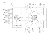
- FIG. 1 is an illustrative plan view showing the layout of the substrate processing apparatus according to the first embodiment of the invention.
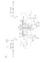
- FIG. 2 is a schematic diagram for explaining the configuration of a wet processing unit provided in the substrate processing apparatus.
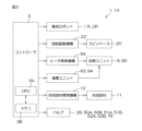
- FIG. 3 is a block diagram for explaining the electrical configuration of the substrate processing apparatus.
- FIG. 4 is a flowchart for explaining substrate processing performed by the substrate processing apparatus.
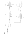
- FIG. 5 is a schematic diagram for explaining the state of the upper surface of the substrate during the substrate processing.
- FIG. 6 is a schematic diagram for explaining an example of a mechanism when etching a layer to be processed exposed from the upper surface of the substrate.
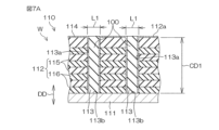
- FIG. 7A is a schematic diagram for explaining an example of the structure of the surface layer portion of the upper surface of the substrate processed by the substrate processing apparatus.
- FIG. 1 is an illustrative plan view showing the layout of the substrate processing apparatus according to the first embodiment of the invention.
- FIG. 2 is a schematic diagram for explaining the configuration of a wet processing unit provided in
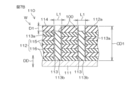
- FIG. 7B is a schematic diagram for explaining a change in structure due to etching of the surface layer portion of the upper surface of the substrate shown in FIG. 7A.
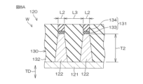
- FIG. 8A is a schematic diagram for explaining another example of the structure of the surface layer portion of the upper surface of the substrate processed by the substrate processing apparatus.
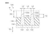
- FIG. 8B is a schematic diagram for explaining a change in structure due to etching of a surface layer portion of the upper surface of the substrate shown in FIG. 8A.
- FIG. 9 is a schematic diagram for explaining a modification of the wet processing unit.
- FIG. 10 is an illustrative plan view showing the layout of the substrate processing apparatus according to the second embodiment of the invention.
- FIG. 10 is an illustrative plan view showing the layout of the substrate processing apparatus according to the second embodiment of the invention.
- FIG. 11 is a schematic diagram for explaining the configuration of a wet processing unit provided in the substrate processing apparatus according to the second embodiment.
- FIG. 12 is a schematic diagram for explaining the configuration of a dry processing unit provided in the substrate processing apparatus according to the second embodiment.
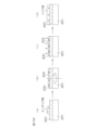
- FIG. 13A is a schematic diagram for explaining the procedure of a time change experiment for observing the time dependence of etching.
- FIG. 13B is a graph showing the results of the time change experiment.
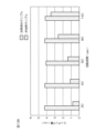
- FIG. 14 is a graph showing the results of a concentration change experiment for observing concentration dependence of etching.
- FIG. 15 is a table showing the results of crystal observation experiments for observing the generation of crystals in the etching solution.
- FIG. 16 is a graph showing the results of a rotational speed change experiment for observing the dependence of etching on the substrate rotational speed.
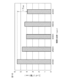
- FIG. 17 is a graph showing the results of a temperature change experiment for observing the heating temperature dependence of etching.
- FIG. 1 is an illustrative plan view showing the layout of a substrate processing apparatus 1 according to the first embodiment of the invention.
- the substrate processing apparatus 1 is a single-wafer type apparatus that processes substrates W one by one.
- the substrate W has a circular shape.
- the substrate W has a pair of main surfaces. At least one of a silicon oxide layer (SiO 2 layer) and a silicon nitride layer (SiN layer) is exposed from at least one of the pair of main surfaces of the substrate W as a layer to be processed.
- the substrate processing apparatus 1 includes a plurality of processing units 2 for processing substrates W, a load port LP on which a carrier C containing a plurality of substrates W to be processed by the processing units 2 is mounted, the load port LP and processing. It includes transport robots IR and CR that transport substrates W between units 2 and controller 3 that controls substrate processing apparatus 1 .
- the transport robot IR transports the substrate W between the carrier C and the transport robot CR.
- the transport robot CR transports the substrate W between the transport robot IR and the processing unit 2 .
- the transport robots IR and CR are arranged on a transport route TR extending from the load ports LP toward the processing units 2 .
- a plurality of processing units 2 have, for example, the same configuration.
- the plurality of treatment units 2 form four treatment towers TW each arranged at four horizontally spaced positions.
- Each processing tower TW includes a plurality of (for example, three) processing units 2 stacked vertically.
- the four processing towers TW are arranged two by two on each side of the transport route TR.
- the processing unit 2 is a wet processing unit 2W that processes the substrate W with a processing liquid.
- examples of the processing liquid supplied toward the substrate W within the wet processing unit 2W include an etching liquid and a rinse liquid.
- Each wet processing unit 2W includes a processing cup 7 and a chamber 4 that accommodates the processing cup 7.
- the chamber 4 is formed with an entrance (not shown) through which the substrate W is loaded and unloaded by the transport robot CR.
- the chamber 4 is provided with a shutter unit (not shown) that opens and closes this entrance.
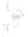
- FIG. 2 is a schematic diagram for explaining the configuration of the wet processing unit 2W.
- the wet processing unit 2W has a spin chuck 5 for rotating the substrate W around the rotation axis A1 while holding the substrate W at a predetermined holding position, and a heating surface 6a facing the lower surface of the substrate W.
- the holding position is a position where the rotation axis A1 coincides with the central axis passing through the center of the upper surface of the substrate W, and the upper surface of the substrate W is horizontal.
- a spin chuck 5 and a plurality of processing liquid nozzles are arranged in a chamber 4 (see FIG. 1) together with a processing cup 7 .
- the spin chuck 5 is surrounded by the processing cup 7.
- the spin chuck 5 includes a spin base 20 that adheres to the lower surface of the substrate W and holds the substrate W at a predetermined holding position, a rotation shaft 21 that extends along the rotation axis A1 and is coupled to the spin base 20, and a rotation shaft. and a rotary drive mechanism 22 for rotating 21 about the rotation axis A1.
- the spin base 20 has an attraction surface 20a that attracts the lower surface of the substrate W.
- the attraction surface 20a is, for example, the upper surface of the spin base 20.
- the attraction surface 20a is, for example, a circular surface through which the rotation axis A1 passes through the center.
- the diameter of the attraction surface 20a is smaller than the diameter of the substrate W. As shown in FIG.
- a suction path 23 is inserted in the spin base 20 and the rotating shaft 21 .
- the suction path 23 has a suction port 23 a exposed from the center of the suction surface 20 a of the spin base 20 .
- the suction path 23 is connected to the suction pipe 24 .
- the suction pipe 24 is connected to a suction device 25 such as a vacuum pump.
- the suction device 25 may constitute a part of the substrate processing apparatus 1 or may be a separate device from the substrate processing apparatus 1 provided in the facility where the substrate processing apparatus 1 is installed.
- the suction pipe 24 is provided with a suction valve 26 for opening and closing the suction pipe 24 .
- a suction valve 26 By opening the suction valve 26 , the substrate W placed on the suction surface 20 a of the spin base 20 is sucked into the suction port 23 a of the suction path 23 .
- the substrate W is sucked by the suction surface 20a from below and held at the holding position.
- the posture of the substrate W held at the holding position is, for example, a posture in which the upper surface of the substrate W is along the horizontal direction.
- the substrate W may be centered by a centering unit (not shown) so that the center axis of the substrate W coincides with the rotation axis A1.
- the rotation drive mechanism 22 includes, for example, an actuator such as an electric motor.
- the rotation drive mechanism 22 rotates the rotation shaft 21 to rotate the spin base 20 .
- the substrate W is rotated around the rotation axis A1 together with the spin base 20 .
- the spin base 20 is an example of a substrate holding member that holds the substrate W at a predetermined holding position.
- the spin chuck 5 is an example of a rotation holding unit that rotates the substrate W around the rotation axis A1 while holding the substrate W at a predetermined holding position.
- the spin chuck 5 is also referred to as a suction rotation unit that rotates the substrate W while the substrate W is attracted to the suction surface 20a.
- the plurality of processing liquid nozzles includes an etchant nozzle 8 that discharges a continuous flow of etchant toward the upper surface of the substrate W held by the spin chuck 5 , and an etching liquid nozzle 8 that discharges a continuous flow of the etchant toward the upper surface of the substrate W held by the spin chuck 5 . and a rinse liquid nozzle 9 for ejecting a continuous stream of rinse liquid toward.
- the etchant discharged from the etchant nozzle 8 contains an etchant as a solute and a solvent that dissolves the etchant.
- the etchant is a substance that has the property of etching the layer exposed from the main surface of the substrate W to be processed.
- the etchant contains ammonium fluoride ( NH4F ).
- the solvent should be able to dissolve the etchant, for example, pure water such as DIW (Deionized Water). Therefore, an aqueous ammonium fluoride solution can be used as the etchant.
- the solvent is not limited to DIW, and can be selected from liquids used as rinse liquids, which will be described later.
- the etchant reacts with the layer to be processed to form a solid layer containing thermally decomposable solids.
- Ammonium fluoride used as an etchant reacts with silicon oxide as a layer to be processed according to chemical reaction formulas 1 and 2 below.
- ammonium fluoride and silicon dioxide react to form a solid layer mainly containing ammonium silicofluoride ((NH 4 ) 2 SiF 6 ) in a solid state. be done.
- ammonium silicofluoride is decomposed by heating. Decomposition of ammonium silicofluoride produces ammonia (NH 3 ), hydrogen fluoride (HF), and silicon tetrafluoride (SiF 4 ). All of these substances are gases at the reaction temperature.
- the layer to be processed contains silicon nitride, a solid layer containing solid-state ammonium silicofluoride is formed.
- the mass percent concentration of the etchant in the etchant is preferably 0.2 wt% or more and less than 10 wt%.
- the mass percent concentration of the etchant in the etching solution is more preferably 0.2 wt% or more and 7.0 wt% or less, even more preferably 2.0 wt% or more and 7.0 wt% or less, and 2.0 wt%. It is even more preferable that the content is 6.0 wt % or more.
- the rinse liquid discharged from the rinse liquid nozzle 9 is, for example, pure water such as DIW.
- the rinse liquid is not limited to DIW.
- the rinsing solution is, for example, carbonated water, electrolytic ion water, hydrochloric acid water with a dilution concentration (for example, 1 ppm or more and 100 ppm or less), ammonia water with a dilution concentration (for example, 1 ppm or more and 100 ppm or less), or , reduced water (hydrogen water).
- each processing liquid nozzle is a fixed nozzle whose position in the vertical and horizontal directions is fixed.
- An etchant pipe 40 for guiding the etchant to the etchant nozzle 8 is connected to the etchant nozzle 8 .
- the etchant pipe 40 is provided with an etchant valve 50A that opens and closes the flow path in the etchant pipe 40 and an etchant flow control valve 50B that adjusts the flow rate of the etchant in the etchant pipe 40 .
- the fact that the valve is provided in the pipe may mean that the valve is interposed in the pipe.
- a rinse liquid pipe 41 that guides the rinse liquid to the rinse liquid nozzle 9 is connected to the rinse liquid nozzle 9 .
- the rinse liquid pipe 41 is provided with a rinse liquid valve 51A that opens and closes the flow path in the rinse liquid pipe 41 and a rinse liquid flow rate adjustment valve 51B that adjusts the flow rate of the rinse liquid in the rinse liquid pipe 41 .
- the rinse liquid valve 51A By opening the rinse liquid valve 51A, the rinse liquid is discharged from the rinse liquid nozzle 9 at a flow rate corresponding to the opening degree of the rinse liquid flow rate control valve 51B.
- the heating unit 6 is a hot plate that heats the substrate W, for example.
- the heating unit 6 includes a plate body 60 facing the substrate W from below and a heater 61 built in the plate body 60 .
- the heating unit 6 is formed, for example, in an annular shape surrounding the spin base 20 .
- the heating surface 6a is configured by the upper surface of the plate body 60, for example.
- the heating surface 6 a may be an annular surface surrounding the spin base 20 .
- the heater 61 may be a resistor built in the plate body 60 . Electric power is supplied to the heater 61 from an energizing unit 63 such as a power supply via a power supply line 62 .
- the set temperature of the heater 61 of the heating unit 6 is, for example, 50° C. or higher and 200° C. or lower.
- the heating unit 6 is vertically moved up and down by the heater lifting mechanism 64 .
- the heater elevating mechanism 64 has a contact heating position (the position indicated by the solid line in FIG. 2) where the substrate W is heated while being in contact with the substrate W, and a non-heating position (the position shown by the solid line in FIG. ), the heating unit 6 is moved up and down.
- the heating unit 6 can heat the substrate W and the liquid on the substrate W to 50° C. or more and 200° C. or less when positioned at the contact heating position.
- the heating unit 6 can also be arranged at a non-contact heating position to heat the substrate W in a non-contact state with the lower surface of the substrate W.
- the non-contact heating position is a position closer to the lower surface of the substrate W than the non-heating position.
- the heater elevating mechanism 64 includes, for example, a ball screw mechanism (not shown) coupled to the plate body 60 and a motor (not shown) that provides driving force to the ball screw mechanism.
- the heater lifting mechanism 64 is also called a heater lifter.
- the processing cup 7 is a member that receives the processing liquid discharged from the substrate W.
- the processing cup 7 includes a vertically extending cylindrical portion 70, an inclined portion 71 extending obliquely upward from the upper end of the cylindrical portion 70, and a substantially annular bottom portion in which the processing liquid received by the inclined portion 71 and the cylindrical portion 70 is guided. 72.
- a sealing member 73 such as a labyrinth seal is provided between the inner peripheral end of the bottom portion 72 and the rotating shaft 21 . The sealing member 73 prevents the processing liquid from leaking from the bottom portion 72 of the processing cup 7 .
- a drainage groove 74 is provided in the bottom portion 72 , and the drainage groove 74 is connected to a drainage pipe 75 .
- a drainage valve 76 is provided in the drainage pipe 75 . By opening the drainage valve 76, the processing liquid is discharged from the drainage pipe 75 as a drainage liquid.
- FIG. 3 is a block diagram for explaining the electrical configuration of the substrate processing apparatus 1.
- the controller 3 has a microcomputer, and controls objects provided in the substrate processing apparatus 1 according to a predetermined control program.
- the controller 3 includes a processor 3A (CPU) and a memory 3B in which control programs are stored.
- the controller 3 is configured to perform various controls for substrate processing by the processor 3A executing a control program.
- the controller 3 controls the transfer robots IR and CR, the rotation drive mechanism 22, the heater elevating mechanism 64, the energization unit 63, the suction valve 26, the etchant valve 50A, the etchant flow rate adjustment valve 50B, the rinse liquid valve 51A, the rinse liquid flow rate It is programmed to control the adjustment valve 51B, the drain valve 76, and the like.
- FIG. 3 Although representative members are shown in FIG. 3, it does not mean that members not shown are not controlled by the controller 3.
- the controller 3 controls each member provided in the substrate processing apparatus 1. can be properly controlled.
- FIG. 3 also shows members described in a modified example and a second embodiment which will be described later, and these members are also controlled by the controller 3 .
- each step shown in FIG. 4 to be described later is executed by the controller 3 controlling each member provided in the substrate processing apparatus 1 .
- the controller 3 is programmed to perform each step shown in FIG. 4, which will be described later.
- FIG. 4 is a flow chart for explaining substrate processing performed by the substrate processing apparatus 1 .
- FIG. 5 is a schematic diagram for explaining the state of the upper surface of the substrate W during substrate processing.
- an etchant supply process (step S1), a liquid film formation process (step S2), a heating process (step S3), a rinse liquid supply process (step S4 ), and the drying step (step S5) are performed.
- step S1 etchant supply process
- step S2 liquid film formation process
- step S3 a heating process
- step S4 rinse liquid supply process
- step S5 drying step
- an unprocessed substrate W is loaded from the carrier C into the processing unit 2 by the transport robots IR and CR (see FIG. 1) and transferred to the spin chuck 5 (loading step).
- the substrate W is held at the holding position by the spin chuck 5 (substrate holding step).
- the substrate W is held by the spin chuck 5 so that the main surface where the layer to be processed is exposed faces upward.
- the spin chuck 5 starts rotating the substrate W while holding the substrate W (rotating step).
- the energization unit 63 is kept energized, and the heater 61 of the heating unit 6 is heated to a set temperature (for example, 50° C. or higher and 200° C. or lower).
- the etchant supply step (step S1) of supplying the etchant to the upper surface of the substrate W is performed. Specifically, the etchant valve 50A is opened. As a result, the etchant is discharged from the etchant nozzle 8 and the etchant lands on the upper surface of the substrate W, as shown in FIG. 5(a). The etchant that has landed on the upper surface of the substrate W spreads over the entire upper surface of the substrate W due to the action of centrifugal force.
- the discharge flow rate of the etchant from the etchant nozzle 8 is, for example, 2000 mL/min. While the etchant is supplied to the upper surface of the substrate W, the substrate W is rotated at, for example, 300 rpm or more and 700 rpm or less.
- a liquid film forming step (step S2) is performed to form a thin liquid film 150 of the etchant on the upper surface of the substrate W.
- the etchant valve 50A is closed after the etchant is discharged from the etchant nozzle 8 for a predetermined period (for example, a period of 5 seconds or more and 15 seconds or less).
- a predetermined period for example, a period of 5 seconds or more and 15 seconds or less.
- the etchant is removed from the upper surface of the substrate W, and a thin liquid film 150 (thin film) of the etchant is formed on the upper surface of the substrate W as shown in FIG. thin film formation process).
- the rotation speed of the substrate W after the ejection of the etchant is stopped, that is, the rotation speed of the substrate W in the liquid film forming process is 2000 rpm or more and 4000 rpm or less.
- the heating process (step S3) for heating the substrate W is started. Specifically, the rotation of the substrate W is stopped, and then the heater elevating mechanism 64 places the heating unit 6 at the contact heating position. As a result, the liquid film 150 on the upper surface of the substrate W is heated through the substrate W, as shown in FIG. 5(c).
- the heating temperature of the liquid film 150 is, for example, the set temperature of the heating unit 6, which is 50° C. or more and 200° C. or less.
- the heating of the liquid film 150 accelerates the etching action of the etchant in the etchant.
- a solid layer 151 is formed on the upper surface of the substrate W by the reaction between the etchant and the layer to be processed.
- the rinse liquid supply step (step S4) of supplying the rinse liquid to the upper surface of the substrate W is performed.
- the heater elevating mechanism 64 arranges the heating unit 6 at the non-heating position. Thereby, the heating of the substrate W is stopped. After that, the rotation of the substrate W is restarted and the rinse liquid valve 51A is opened.
- the rinse liquid is discharged from the rinse liquid nozzle 9, and the rinse liquid lands on the upper surface of the substrate W in the rotating state.
- the rinse liquid that has landed on the upper surface of the substrate W spreads over the entire upper surface of the substrate W due to the action of centrifugal force.
- the solid layer 151 on the upper surface of the substrate W is discharged to the outside of the substrate W while being dissolved in the rinsing liquid.
- the discharge flow rate of the rinse liquid from the rinse liquid nozzle 9 is, for example, 2000 mL/min. While the rinse liquid is being supplied to the upper surface of the substrate W, the substrate W is rotated at, for example, 1000 rpm or more and 2000 rpm or less.
- a drying step (step S5) is performed to dry the upper surface of the substrate W by rotating the substrate W at high speed. Specifically, the supply of the rinse liquid to the upper surface of the substrate W is stopped by closing the rinse liquid valve 51A.
- the rotation drive mechanism 22 accelerates the rotation of the substrate W, and the substrate W is rotated at high speed (eg, 1500 rpm). As a result, a large centrifugal force acts on the rinse liquid adhering to the substrate W, and the rinse liquid is shaken off around the substrate W.
- high speed eg, 1500 rpm
- the rotation drive mechanism 22 stops the rotation of the substrate W.
- the transport robot CR enters the processing unit 2, receives the processed substrate W from the spin chuck 5, and carries it out of the processing unit 2 (carrying-out step).
- the substrate W is transferred from the transport robot CR to the transport robot IR and stored in the carrier C by the transport robot IR.
- the layer to be processed includes at least one of a silicon oxide layer and a silicon nitride layer, and the etchant contains ammonium fluoride as an etchant. Therefore, by heating, the layer to be processed and the etchant present on the main surface of the substrate W can be rapidly reacted, and the time dependence of the etching of the layer to be processed can be reduced. That is, saturated atomic layer etching can be achieved.
- the substrate W is rotated after the etchant supply process and before the heating process. Therefore, the amount of the etchant on the upper surface of the substrate W can be appropriately reduced, and the total amount of the etchant present on the upper surface of the substrate W can be controlled. If the total amount of the etchant can be controlled, the etching amount of the layer to be processed can be easily controlled. In particular, by rotating the substrate W at a rotation speed of 2000 rpm or more and 4000 rpm or less, the total amount of the etchant present on the upper surface of the substrate W can be controlled with high accuracy.
- the mass percent concentration of the etchant in the etchant is 0.2 wt % or more and less than 10 wt %, saturated atomic layer etching can be easily achieved.
- the heating temperature in the heating step is 50° C. or higher and 200° C. or lower, the layer to be processed and the etchant present on the main surface of the substrate can be reacted particularly quickly.
- FIG. 6 is a schematic diagram for explaining an example of a mechanism when etching the processing target layer 100 exposed from the upper surface of the substrate W.
- a liquid film 150 is formed on the upper surface of the substrate W as shown in FIG. 6(a).
- a solid layer 151 is formed by the reaction between the etchant in the etchant on the upper surface of the substrate W and the layer 100 to be processed.
- the formation of the solid layer 151 is promoted as shown in FIG. 6(b).
- the etching progresses as the etchant permeates the solid layer 151 and reaches the processing target layer 100 .
- the thickness T of the solid layer 151 increases.
- the reaction between the etchant and the processing target layer 100 is promoted (reaction promotion step).
- the decomposition product of the solid layer 151 is gas
- the gas diffuses into the atmosphere.
- the product of the reaction between the etchant and the layer 100 to be processed is removed from the reaction system.
- the decomposition of solid layer 151 is accelerated to increase the amount of products of the pyrolysis reaction.
- the etching is stopped when the etching of the processing target layer 100 progresses until most of the etchant on the upper surface of the substrate W is consumed. Since at least a part of the solid layer 151 formed by the reaction between the etchant and the layer 100 to be processed is thus removed by heating, the reaction between the etchant and the layer 100 to be processed is promoted.
- Decomposition converts ammonium silicofluoride ((NH 4 ) 2 SiF 6 ) into various decomposition products (ammonia, hydrogen fluoride, silicon tetrafluoride). Since various decomposition products are gaseous at the reaction temperature, the decomposition products diffuse into the atmosphere. As a result, the product of the reaction between the etchant and the layer 100 to be processed (reaction represented by Chemical Reaction Formula 1) is removed from the reaction system.
- the etching depth D (see FIG. 6D) of the layer 100 to be processed is proportional to the total amount of etchant in the etchant present on the upper surface of the substrate W at the start of the heating process. Therefore, by controlling the amount of the etchant present on the upper surface of the substrate W at the start of the heating process, the etching depth D can be accurately controlled.
- FIG. 7A is a schematic diagram for explaining an example of the structure of the surface layer portion 110 on the upper surface of the substrate W processed by the substrate processing apparatus 1.
- FIG. 7B is a schematic diagram for explaining a change in structure due to etching of the surface layer portion 110 on the upper surface of the substrate W shown in FIG. 7A.
- the surface layer portion 110 on the upper surface of the substrate W includes a semiconductor layer 111, a laminate 112 formed on the semiconductor layer 111, and a plurality of channels 113 formed by digging the surface of the laminate 112. , a plurality of layers to be processed 100 respectively embedded in the plurality of channels 113, and a coating layer 114 interposed between the sidewalls 113a of the channels 113 and the layers to be processed 100 and covering the sidewalls 113a of the channels 113.
- the depth CD1 of the channel 113 is, for example, 32 atomic layers or more and 96 atomic layers or less.
- the channel 113 has, for example, a circular shape when viewed from the depth direction DD of the channel 113 .
- Width L1 of channel 113 is, for example, 50 nm or more and 90 nm or less.
- the semiconductor layer 111 is made of Si single crystal, for example.
- Laminate 112 has a plurality of first insulating layers 115 and a plurality of second insulating layers 116 .
- the first insulating layers 115 and the second insulating layers 116 are alternately arranged in the depth direction DD of the channel 113 .
- the first insulating layer 115 is, for example, a silicon oxide layer
- the second insulating layer 116 is, for example, a silicon nitride layer.
- a fine concavo-convex pattern is formed on the surface layer portion 110 by the side walls 113 a of the channels 113 , the bottom walls 113 b of the channels 113 , and the tip surfaces 112 a of the laminate 112 .
- the covering layer 114 covers the side wall 113a of the channel 113 and the top end surface 112a of the laminate 112 . Therefore, exposure of the laminate 112 to the etchant can be suppressed.
- the substrate W having the surface layer portion 110 having such a configuration there is a substrate used in the manufacturing process of a three-dimensional NAND flash memory.
- part of the layer 100 to be processed within the channel 113 is etched to achieve the desired etching depth D1, as shown in FIG. 7B.
- the layer 100 to be processed can be etched by wet etching, damage to the fine uneven pattern and excessive etching of the layer 100 to be processed, which are problems when using dry etching such as reactive ion etching, can be suppressed. can be done.
- the damage to the fine concavo-convex pattern means, for example, that the corners of the front end surface 112a of the laminate 112 are shaved to have a rounded shape (curved shape).
- FIG. 8A is a schematic diagram for explaining another example of the structure of the surface layer portion 120 on the upper surface of the substrate W processed by the substrate processing apparatus 1.
- FIG. 8B is a schematic diagram for explaining a change in structure due to etching of the surface layer portion 120 on the upper surface of the substrate W shown in FIG. 8A.
- the surface layer portion 120 on the upper surface of the substrate W includes a semiconductor layer 121, a plurality of structures 122 formed on the semiconductor layer 121, and a processing target layer 130 covering the plurality of structures 122.
- the processing target layer 130 has a first processing target layer 131 formed on each structure 122 and a second processing target layer 132 positioned between the structures 122 .
- the semiconductor layer 121 and the plurality of structures 122 are made of Si single crystal, for example.
- the first processing target layer 131 has, for example, a first layer 133 made of a silicon oxide layer and a second layer 134 made of a silicon nitride layer formed on the first layer 133 .
- the second processing target layer 132 is, for example, a silicon oxide layer.
- the second processing target layer 132 is positioned between the adjacent structures 122 so as to be in contact with the first processing target layer 131 and the structures 122 .
- the structure 122 has a line shape (strip shape) when viewed from the height direction TD of the structure 122, and the plurality of structures 122 are arranged at intervals.
- Width L2 of structure 122 is the width in the lateral direction (arrangement direction of structure 122) of structure 122 when viewed from height direction TD of structure 122, and is, for example, 5 nm or more and 22 nm or less.
- a width L3 of the gap between the structures 122 is, for example, 24 nm or more and 60 nm or less.
- a fine concavo-convex pattern is formed on the surface layer portion 120 by a plurality of structures 122 .
- the substrate W having the surface layer portion 120 having such a configuration there is a substrate used in a CMOS manufacturing process.
- part of the processing target layer 130 is etched to achieve the desired etching depth D2.
- the entire first processing target layer 131 is removed by etching.
- a portion of the second processing target layer 132 is removed by etching such that the surface of the second processing target layer 132 is positioned closer to the semiconductor layer 121 than the tip portions 122 a of the plurality of structures 122 .
- the layer to be processed 130 after being etched functions as an interlayer insulating film. Since the layer 130 to be processed can be etched by wet etching, damage to the fine uneven pattern and excessive etching of the layer 130 to be processed can be suppressed.
- the structure 122 has a protrusion 122b protruding from the second layer 132 to be processed.
- a height T2 of the projecting portion 122b (the distance in the height direction TD from the surface of the second processing target layer 132 after etching to the tip portion 122a) is, for example, 34 nm or more and 60 nm or less.
- FIG. 9 is a schematic diagram for explaining a modification of the wet processing unit 2W.
- the wet processing unit 2W directs the heating gas toward the upper surface of the substrate W to heat the substrate W and the liquid film 150 on the substrate W instead of the heating unit 6 (see FIG. 2). It may also include a heated gas nozzle 10 for supplying.
- the wet processing unit 2W shown in FIG. 9 includes a facing member 11 having a facing surface 11a that faces the upper surface of the substrate W, and a facing member elevating mechanism 12 that moves the facing member 11 up and down.
- the heated gas nozzle 10 has a discharge port 10a exposed from the facing surface 11a.
- the heated gas discharged from the heated gas nozzle 10 is, for example, an inert gas such as nitrogen gas, air, or a mixed gas thereof.
- the inert gas is not limited to nitrogen gas, and may contain rare gas such as argon gas.
- the temperature of the heated gas is, for example, 50°C or higher and 200°C or lower.
- a heated gas pipe 42 that guides the heated gas to the heated gas nozzle 10 is connected to the heated gas nozzle 10 .
- the heated gas pipe 42 is provided with a heated gas valve 52A that opens and closes the flow path in the heated gas pipe 42 and a heated gas flow rate adjustment valve 52B that adjusts the flow rate of the heated gas in the heated gas pipe 42 .
- the heating gas valve 52A By opening the heating gas valve 52A, the heating gas is discharged from the heating gas nozzle 10 at a flow rate corresponding to the degree of opening of the heating gas flow control valve 52B.
- the facing member 11 includes a circular facing portion 80 facing the upper surface of the substrate W and an annular portion 81 extending downward from the peripheral edge of the facing portion 80 .
- the facing surface 11 a is, for example, the lower surface of the facing portion 80 .
- the opposing member 11 is moved by the opposing member elevating mechanism 12 to a close position near the upper surface of the substrate W (the position indicated by the two-dot chain line in FIG. 9) and a separated position above the close position (the position indicated by the solid line in FIG. 9). ).
- the annular portion 81 faces the substrate W in the horizontal direction.
- the opposing member elevating mechanism 12 includes, for example, a ball screw mechanism (not shown) coupled to the opposing member 11 and a motor (not shown) that provides driving force to the ball screw mechanism.
- the opposing member elevating mechanism 12 is also called an opposing member lifter.
- the facing portion 80, the annular portion 81 and the substrate W form a processing space SP.
- the gas in the processing space SP can be quickly replaced with the heated gas.
- the substrate W and the liquid film 150 can be rapidly heated.
- FIG. 10 is an illustrative plan view showing the layout of the substrate processing apparatus 1A according to the second embodiment.
- the plurality of processing units 2 provided in the substrate processing apparatus 1A includes a plurality of dry processing units 2D in addition to a plurality of wet processing units 2W.
- the two processing towers TW on the transfer robot IR side are composed of a plurality of wet processing units 2W
- the two processing towers TW on the opposite side of the transfer robot IR are composed of a plurality of dry processing units 2W. It is composed of the unit 2D.
- the dry processing unit 2D includes a thermal processing chamber 90 located within the chamber 4 and heating the substrate W therein.
- FIG. 11 is a schematic diagram for explaining the configuration of the wet processing unit 2W according to the second embodiment. As shown in FIG. 11, unlike the first embodiment, the wet processing unit 2W according to the second embodiment is not provided with a structure for heating the substrate W. As shown in FIG. 11, unlike the first embodiment, the wet processing unit 2W according to the second embodiment is not provided with a structure for heating the substrate W. As shown in FIG. 11, unlike the first embodiment, the wet processing unit 2W according to the second embodiment is not provided with a structure for heating the substrate W. As shown in FIG.
- FIG. 12 is a schematic diagram for explaining the configuration of the dry processing unit 2D.
- the dry processing unit 2D further includes a heating unit 91 that is accommodated in the heat treatment chamber 90 and has a heating surface 91a on which the substrate W is placed.
- the heating unit 91 has the shape of a disk-shaped hot plate.
- Heating unit 91 includes plate body 92 and heater 93 .
- the upper surface of the plate body 92 constitutes a heating surface 91a.
- the heater 93 may be a resistor built into the plate body 92 .
- the heater 93 can heat the substrate W to a temperature substantially equal to the temperature of the heater 93 .
- the heater 93 is heated to a set temperature (for example, 50° C. or higher and 200° C. or lower).
- the heater 93 is connected to an energization unit 94 such as a power source, and the temperature of the heater 93 changes within a predetermined temperature range by adjusting the current supplied from the energization unit 94. do.
- the heat treatment chamber 90 includes a chamber body 90A that opens upward, and a lid 90B that moves up and down above the chamber body 90A and closes the opening of the chamber body 90A.
- the transfer robot CR can access the inside of the heat treatment chamber 90 while the opening of the chamber main body 90A is open (the state indicated by the two-dot chain line in FIG. 12).
- the dry processing unit 2D further includes a plurality of lift pins 96 that pass through the plate body 92 and move up and down.
- the plurality of lift pins 96 has an upper position (position indicated by a two-dot chain line in FIG. 12) supporting the substrate W above the heating surface 91a, and a lower position where the tip (upper end) is immersed below the heating surface 91a. It is possible to move up and down between positions (positions indicated by solid lines in FIG. 12).
- step S4 substrate processing (see FIGS. 4 and 5) similar to that of the first embodiment can be performed.
- step S4 the substrate W is transferred between the wet processing unit 2W and the dry processing unit 2D.
- step S4 the plurality of lift pins 96 are placed at the lower position, and the opening of the chamber main body 90A is closed by the lid 90B (the state indicated by solid lines in FIG. 12).
- the liquid film 150 is heated via W.
- FIG. 13A is a schematic diagram for explaining the procedure of a time change experiment for observing the time dependence of etching. In the time change experiment, the following procedures (a) to (d) were performed.
- a 2.5 cm square small piece substrate (hereinafter referred to as “small piece substrate 200”) on which a silicon oxide film having a thickness of 100 nm is formed is placed on the heater 201, and the main piece of the small piece substrate 200 is heated.
- 1 mL of an ammonium fluoride aqueous solution (etching solution) was supplied to the surface.
- the mass percent concentration of ammonium fluoride (etching agent) in the aqueous ammonium fluoride solution is 2 wt%.
- the small substrate 200 was rotated by rotating the heater 201 for a predetermined rotation time.
- the aqueous ammonium fluoride solution on the small substrate piece 200 spreads over the entire main surface of the small substrate piece 200 , forming a thin film 202 of the ammonium fluoride aqueous solution on the main surface of the small substrate piece 200 .
- the rotation of the small substrate piece 200 was started at 500 rpm, and the rotation of the small substrate piece 200 was accelerated stepwise so that the rotational speed of the small substrate piece 200 reached 3000 rpm 20 seconds after the start of rotation.
- Five types of small substrates 200 were prepared with rotation times of 30 seconds, 40 seconds, 60 seconds, 80 seconds, and 140 seconds, respectively.
- each small substrate 200 was rinsed with a rinse liquid.
- FIG. 13B is a graph showing the results of the time change experiment, showing the relationship between the rotation time of the small substrate 200 and the amount of etching.
- the etching amount was the same at any rotation time, and was about 4.0 nm to 4.2 nm.
- the etching amount increased with the lapse of time and gradually approached 4.0 nm. Therefore, it can be inferred that etching is promoted by heating.
- the etchant is heated through the small substrate 200, the etching is completed at least when the rotation time is 30 seconds, indicating that the dependence of the etching amount on the rotation time is extremely low.
- the small substrate piece 200 was placed on the heater 201, and 1 m of an ammonium fluoride aqueous solution was supplied to the main surface of the small piece substrate 200.
- Five kinds of small substrates 200 were prepared by setting the concentration of ammonium fluoride in the ammonium fluoride aqueous solution supplied to the small substrates 200 to 2 wt %, 4 wt %, 6 wt %, and 10 wt %, respectively.
- the small substrate 200 was rotated by rotating the heater 201 for a predetermined rotation time.
- the aqueous solution of ammonium fluoride on the small substrate piece 200 spreads over the entire main surface of the small substrate piece 200 , forming an ammonium fluoride thin film 202 on the main surface of the small substrate piece 200 .
- the rotation of the small substrate pieces 200 was started at 500 rpm, and the rotation of the small substrate pieces 200 was accelerated stepwise so that the rotational speed of the small substrate pieces 200 reached 3000 rpm 20 seconds after the start of rotation.
- the small substrate 200 was rotated until 80 seconds had passed.
- each small substrate 200 was heated by the heater 201 . Heating was performed at 200° C. for 180 seconds.
- each small substrate 200 was rinsed with a rinse liquid.
- FIG. 14 is a graph showing the results of concentration change experiments. As shown in FIG. 14, when the ammonium fluoride concentration is 2 wt %, the etching amount is about 4.1 nm, and when the ammonium fluoride concentration is 4 wt %, the etching amount is about 6.1 nm. Met. When the ammonium fluoride concentration was 6 wt %, the etching amount was about 7.5 nm, and when the ammonium fluoride concentration was 10 wt %, the etching amount was about 12.5 nm. Thus, the etching amount increased as the concentration of ammonium fluoride increased. It was shown that the amount of etching varied depending on the concentration of the etchant. The etching amount difference in the concentration range of 2 wt % to 10 wt % was 8.4 nm.
- the small substrate piece 200 was placed on the heater 201, and 1 mL of an ammonium aqueous solution was supplied to the main surface of the small piece substrate 200.
- Five kinds of small substrates 200 were prepared by setting the concentration of ammonium fluoride in the ammonium fluoride aqueous solution supplied to the small substrates 200 to 2 wt %, 4 wt %, 6 wt %, 10 wt %, and 15 wt %.
- the small substrate 200 was rotated by rotating the heater 201 for a predetermined rotation time. At that time, the rotation of the small substrate piece 200 was started at 500 rpm, and the rotation of the small substrate piece 200 was accelerated stepwise so that the rotational speed of the small substrate piece 200 reached 3000 rpm 20 seconds after the start of rotation.
- Five kinds of small piece substrates 200 were prepared with rotation times of 30 seconds, 40 seconds, 50 seconds, 60 seconds, and 80 seconds, respectively, for the small piece substrates 200 supplied with aqueous ammonium fluoride solutions of various concentrations. .
- each small substrate 200 was heated by the heater 201 . Heating was performed at 200° C. for 180 seconds.
- each small substrate 200 was rinsed with a rinse liquid.
- FIG. 15 is a table showing the results of crystal observation experiments. As shown in FIG. 15, when the mass percent concentrations of ammonium fluoride in the aqueous solution of ammonium fluoride were 2 wt %, 4 wt %, and 6 wt %, the generation of crystals was observed regardless of the rotation time of the small piece substrate 200 . it wasn't. On the other hand, when the mass percent concentration of ammonium fluoride in the ammonium fluoride aqueous solution was 10 wt %, crystal formation was observed when the rotation time was longer than 30 seconds.
- the mass percent concentration of ammonium fluoride in the etchant is less than 10 wt %, the silicon oxide film can be sufficiently etched while maintaining good in-plane etching uniformity.
- the mass percent concentration of ammonium fluoride in the etching solution is 2 wt % or more and less than 10 wt %, such effects are likely to be produced.
- the mass percent concentration of ammonium fluoride in the etchant is 2 wt % or more and 6 wt % or less, such effects are more likely to be exhibited.
- the small substrate 200 was rotated by rotating the heater 201 for a predetermined rotation time.
- the aqueous solution of ammonium fluoride on the small substrate piece 200 spreads over the entire main surface of the small substrate piece 200 , forming an ammonium fluoride thin film 202 on the main surface of the small substrate piece 200 .
- the small substrate pieces 200 were started to rotate at 500 rpm, and the rotation of the small substrate pieces 200 was accelerated so that the rotational speed of the small substrate pieces 200 reached a predetermined thinning speed about 5 seconds after the start of rotation.
- the rotation of the small piece substrate 200 at the thinning speed was continued until about 80 seconds had elapsed after the start of rotation.
- Five types of small piece substrates 200 were prepared with thinning speeds of 2000 rpm, 2500 rpm, 3000 rpm, 3500 rpm and 4000 rpm, respectively.
- each small substrate 200 was rinsed with a rinse liquid.
- the removal amount (etching amount) of the silicon oxide film of these five types of small substrates 200 was measured using an SEM or the like.
- FIG. 16 is a graph showing the results of the rotation speed change experiment.
- the etching amount tended to decrease as the thinning speed increased in the range of 2000 rpm or more and 3000 rpm or less. Specifically, when the thinning speed is 2000 rpm, the etching amount is about 5.6 nm, and when the thinning speed is 2500 rpm, the etching amount is about 4.8 nm, and the thinning speed is 3000 rpm. , the etching amount was about 4.1 nm. Thus, it was shown that the etching amount changes depending on the thinning speed.
- the etching amount was generally constant regardless of the thinning speed.
- the reason for this is that when the thinning speed is 3000 rpm, the ammonium fluoride aqueous solution on the small piece substrate 200 is thinned to the limit, and even if the rotation speed is increased, the amount of the ammonium fluoride aqueous solution on the small piece substrate 200 does not reach the limit. Since no change occurred, it is conceivable that the amount of etching did not change in the above rotation speed range.
- the change in the etching amount due to the change in the thinning rate was about 1.7 nm.
- the amount was up to about 8.4 nm. Therefore, it is presumed that the etching amount can be finely controlled by adjusting the thinning speed, that is, by controlling the rotational speed of the substrate.
- the small substrate 200 was rotated by rotating the heater 201 for a predetermined rotation time.
- the ammonium fluoride aqueous solution on the small substrate piece 200 spreads over the entire main surface of the small substrate piece 200 , forming a thin film of ammonium fluoride on the main surface of the small substrate piece 200 .
- the rotation of the small substrate pieces 200 was started at 500 rpm, and the rotation of the small substrate pieces 200 was accelerated stepwise so that the rotational speed of the small substrate pieces 200 reached 3000 rpm 20 seconds after the start of rotation.
- the small substrate 200 was rotated until 80 seconds had passed.
- the small substrate 200 was heated by the heater 201 .
- Four types of small substrates 200 were prepared at heating temperatures of 50° C., 80° C., 150° C., and 180° C., respectively.
- each small substrate 200 was rinsed with a rinse liquid.
- FIG. 17 is a graph showing the results of the temperature change experiment. As shown in FIG. 17, the etching amount was about 4.5 nm at any heating temperature. Therefore, it was shown that sufficient etching can be achieved regardless of the heating temperature within the range of at least 50° C. or higher and 180° C. or lower.
- the upper surface of the substrate W is subjected to substrate processing.
- substrate processing may be performed on the lower surface of the substrate W as well.
- the spin chuck 5 is a vacuum chuck type spin chuck that causes the spin base 20 to absorb the substrate W.
- the spin chuck 5 may be a gripping type spin chuck that grips the peripheral edge of the substrate W with a plurality of chuck pins.
- the spin chuck 5 does not necessarily hold the substrate W horizontally. 3, the spin chuck 5 may hold the substrate W vertically, or may hold the substrate W such that the upper surface of the substrate W is inclined with respect to the horizontal plane.
- the solid formed by the reaction between the etchant in the etchant and the layer to be processed is decomposed by heating, thereby promoting the reaction between the etchant and the layer to be processed.
- the substance formed by the reaction between the etchant and the layer to be processed does not decompose and becomes a gas (mainly by sublimation) due to a change in state. may be promoted.
- the rotation of the substrate W may be stopped during the etchant supply step.
- a plurality of fluids are respectively discharged from a plurality of nozzles.
- the mode of discharging each fluid is not limited to the above-described embodiments.
- each processing liquid nozzle may be a moving nozzle that can move in the horizontal direction.
- all the processing liquid nozzles may be configured to be moved together by a single nozzle moving mechanism.
- all the fluids may be discharged toward the upper surface of the substrate W from a single nozzle.
- each pipe may be provided with a flow control valve (not shown) for adjusting the flow rate of the processing liquid discharged from the corresponding processing liquid nozzle.
- the controller 3 controls the substrate processing apparatus 1 as a whole.
- the controllers that control each member of the substrate processing apparatus 1 may be distributed in a plurality of locations.
- the controller 3 does not need to directly control each member, and signals output from the controller 3 may be received by a slave controller that controls each member of the substrate processing apparatus 1 .
- the substrate processing apparatus 1 includes the transfer robots IR and CR, a plurality of processing units 2, and the controller 3.
- the substrate processing apparatus 1 may be composed of a single processing unit 2 and controller 3 and may not include a transfer robot.
- the substrate processing apparatus 1 may be configured with only a single processing unit 2 .
- the processing unit 2 may be an example of a substrate processing apparatus.
Landscapes
- Weting (AREA)
- Chemical & Material Sciences (AREA)
- Chemical Kinetics & Catalysis (AREA)
- General Chemical & Material Sciences (AREA)
Abstract
基板処理方法は、酸化シリコン層および窒化シリコン層の少なくとも一方が処理対象層として露出する主面を有する基板を処理する。前記基板処理方法は、前記処理対象層をエッチングするエッチング剤としてフッ化アンモニウムを含有するエッチング液を前記基板の前記主面に供給するエッチング液供給工程と、前記エッチング液供給工程の後、前記基板の前記主面上の前記エッチング液を加熱する加熱工程と、前記加熱工程の後、前記基板の前記主面にリンス液を供給するリンス液供給工程とを含む。
Description
この出願は、2021年12月17日提出の日本国特許出願2021-205312号に基づく優先権を主張しており、この出願の全内容はここに引用により組み込まれるものとする。
この発明は、基板を処理する基板処理方法に関する。処理の対象となる基板には、たとえば、半導体ウェハ、液晶表示装置および有機EL(Electroluminescence)表示装置等のFPD(Flat Panel Display)用基板、光ディスク用基板、磁気ディスク用基板、光磁気ディスク用基板、フォトマスク用基板、セラミック基板、太陽電池用基板等が含まれる。
下記特許文献1には、水素を含有する第1グループのフルオロカーボン(たとえば、CHF3)および水素を含有しない第2グループのフルオロカーボン(たとえば、C4F8)を含むフルオロカーボンガス、CO等の炭素-酸素含有ガス、ならびに、N2等の窒素含有ガスを備えるプロセスガスによって、誘電層を備える基板をエッチングする基板処理が開示されている。
特許文献1には、上述の基板処理によって、高選択率のエッチングを達成できることが開示されている。しかしながら、特許文献1に開示されている基板処理では、所望のエッチング深さでプロセスガスと基板との反応を停止させることは難しい。この発明の一実施形態は、エッチング深さを精度良く制御できる基板処理方法を提供する。
この発明の一実施形態は、酸化シリコン層および窒化シリコン層の少なくとも一方が処理対象層として露出する主面を有する基板を処理する基板処理方法を提供する。前記基板処理方法は、前記処理対象層をエッチングするエッチング剤としてフッ化アンモニウムを含有するエッチング液を前記基板の前記主面に供給するエッチング液供給工程と、前記エッチング液供給工程の後、前記基板の前記主面上の前記エッチング液を加熱する加熱工程と、前記加熱工程の後、前記基板の前記主面にリンス液を供給するリンス液供給工程とを含む。
この方法によれば、処理対象層が、酸化シリコン層および窒化シリコン層の少なくとも一方であり、エッチング液が、エッチング剤としてフッ化アンモニウムを含有する。そのため、加熱によって、処理対象層と、基板の主面上に存在するエッチング剤とを速やかに反応させることができ、処理対象層のエッチングの時間依存性を低減できる。すなわち、飽和原子層エッチングを達成できる。
飽和原子層エッチングは、一定のプロセス時間でエッチングが停止して、エッチングの深さを制御できるエッチングである。飽和原子層エッチングを複数サイクル繰り返すことで、所望のエッチング深さを簡単に実現できる。具体的には、1サイクルが数十秒以内に停止し、数nmから数十nmのエッチング深さを実現できる。
この発明の一実施形態では、前記基板処理方法が、前記エッチング液供給工程における前記基板の前記主面へのエッチング液の供給を停止した後で、かつ、前記加熱工程の前に、前記基板の前記主面の中心部を通る中心軸線のまわりに前記基板を回転させる回転工程をさらに含む。
この方法によれば、基板の主面へのエッチング液の供給が停止された後、基板が回転される。そのため、基板の主面上のエッチング液の量を適度に低減し、基板の主面上に存在するエッチング剤の総量を制御することができる。エッチング剤の総量を制御できれば、処理対象層のエッチング量を制御し易い。特に、2000rpm以上でかつ4000rpm以下の回転速度で基板を回転させることで、基板の主面上に存在するエッチング剤の総量を精度良く制御できる。
この発明の一実施形態では、前記基板の主面に供給される前記エッチング液における前記エッチング剤の質量パーセント濃度が、0.2wt%以上10wt%未満である。エッチング液におけるエッチング剤の質量パーセント濃度が、0.2wt%以上10wt%未満であれば、飽和原子層エッチングを達成し易い。
この発明の一実施形態では、前記加熱工程において、前記基板が、50℃以上200℃以下に加熱される。エッチング液の加熱温度が50℃以上200℃以下であれば、処理対象層と、基板の主面上に存在するエッチング剤とを特に速やかに反応させることができる。
この発明の一実施形態では、前記処理対象層のエッチング深さが、前記加熱工程の開始時に前記基板の主面上に存在する前記エッチング液中の前記エッチング剤の総量に比例する。そのため、加熱工程の開始時に基板の主面上に存在するエッチング液の量を制御すれば、エッチング深さを精度良く制御できる。
この発明の一実施形態では、前記加熱工程が、前記基板の前記主面上の前記エッチング液中の前記エッチング剤と前記処理対象層との反応によって前記処理対象層上に形成される固体層を加熱によって除去することで、前記エッチング剤と前記処理対象層との反応を促進する反応促進工程を含む。
この方法によれば、エッチング剤と処理対象層との反応によって形成される固体層が加熱によって除去されるので、エッチング剤と処理対象層との反応が促進される。そのため、処理対象層と、基板の主面上に存在するエッチング剤とを一層速やかに反応させることができる。
この発明の一実施形態において、前記基板は、絶縁層と、前記絶縁層の表面を掘り下げることにより形成され前記処理対象層が埋設されるチャネルと、前記処理対象層と前記チャネルの側壁との間に介在し前記チャネルの側壁を被覆する被覆層とをさらに有していてもよい。また、前記基板は、半導体層と、前記半導体層上に形成された複数の構造体であって、当該構造体同士の間に前記処理対象層が位置する複数の構造体とをさらに有していてもよい。
本発明における前述の、またはさらに他の目的、特徴および効果は、添付図面を参照して次に述べる実施形態の説明により明らかにされる。
<第1実施形態に係る基板処理装置の構成>
図1は、本発明の第1実施形態に係る基板処理装置1のレイアウトを示す図解的な平面図である。
図1は、本発明の第1実施形態に係る基板処理装置1のレイアウトを示す図解的な平面図である。
基板処理装置1は、基板Wを1枚ずつ処理する枚葉式の装置である。この実施形態では、基板Wは、円形状を有する。基板Wは一対の主面を有する。基板Wの一対の主面のうちの少なくとも一方の主面から、酸化シリコン層(SiO2層)および窒化シリコン層(SiN層)の少なくとも一が処理対象層として露出する。基板処理装置1は、基板Wを処理する複数の処理ユニット2と、処理ユニット2で処理される複数枚の基板Wを収容するキャリアCが載置されるロードポートLPと、ロードポートLPと処理ユニット2との間で基板Wを搬送する搬送ロボットIRおよびCRと、基板処理装置1を制御するコントローラ3とを備える。
搬送ロボットIRは、キャリアCと搬送ロボットCRとの間で基板Wを搬送する。搬送ロボットCRは、搬送ロボットIRと処理ユニット2との間で基板Wを搬送する。搬送ロボットIRおよびCRは、複数のロードポートLPから複数の処理ユニット2に向かって延びる搬送経路TR上に配置されている。
複数の処理ユニット2は、たとえば、同様の構成を有している。複数の処理ユニット2は、水平に離れた4つの位置にそれぞれ配置された4つの処理タワーTWを形成している。各処理タワーTWは、上下方向に積層された複数(たとえば、3つ)の処理ユニット2を含む。4つの処理タワーTWは、搬送経路TRの両側に2つずつ配置されている。
処理ユニット2は、処理液で基板Wを処理するウェット処理ユニット2Wである。詳しくは後述するが、ウェット処理ユニット2W内で基板Wに向けて供給される処理液としては、エッチング液、リンス液等が挙げられる。
各ウェット処理ユニット2Wは、処理カップ7と、処理カップ7を収容するチャンバ4とを備える。チャンバ4には、搬送ロボットCRによって、基板Wを搬入したり基板Wを搬出したりするための出入口(図示せず)が形成されている。チャンバ4には、この出入口を開閉するシャッタユニット(図示せず)が備えられている。
図2は、ウェット処理ユニット2Wの構成を説明するための模式図である。
ウェット処理ユニット2Wは、基板Wを所定の保持位置に保持しながら、回転軸線A1まわりに基板Wを回転させるスピンチャック5と、基板Wの下面に対向する加熱面6aを有し、基板Wを加熱する加熱ユニット6と、スピンチャック5に保持されている基板Wの上面(上側の主面)に向けて処理液を吐出する複数の処理液ノズル(エッチング液ノズル8およびリンス液ノズル9)とをさらに備える。保持位置は、回転軸線A1が基板Wの上面の中心部を通る中心軸線と一致する位置であり、基板Wの上面が水平な位置である。
スピンチャック5、および、複数の処理液ノズルは、処理カップ7とともにチャンバ4(図1を参照)内に配置されている。
スピンチャック5は、処理カップ7に取り囲まれている。スピンチャック5は、基板Wの下面に吸着し基板Wを所定の保持位置に保持するスピンベース20と、回転軸線A1に沿って延び、スピンベース20に結合されている回転軸21と、回転軸21を回転軸線A1のまわりに回転させる回転駆動機構22とを含む。
スピンベース20は、基板Wの下面に吸着する吸着面20aを有する。吸着面20aは、たとえば、スピンベース20の上面である。吸着面20aは、たとえば、その中心部を回転軸線A1が通る円形状面である。吸着面20aの直径は基板Wの直径よりも小さい。
スピンベース20および回転軸21には、吸引経路23が挿入されている。吸引経路23は、スピンベース20の吸着面20aの中心から露出する吸引口23aを有する。吸引経路23は、吸引配管24に連結されている。吸引配管24は、真空ポンプ等の吸引装置25に連結されている。吸引装置25は、基板処理装置1の一部を構成していてもよいし、基板処理装置1を設置する施設に備えられた基板処理装置1とは別の装置であってもよい。
吸引配管24には、吸引配管24を開閉する吸引バルブ26が設けられている。吸引バルブ26を開くことによって、スピンベース20の吸着面20aに配置された基板Wが吸引経路23の吸引口23aに吸引される。それによって、基板Wは、吸着面20aに下方から吸着されて、保持位置に保持される。保持位置に保持されている基板Wの姿勢は、たとえば、基板Wの上面が水平方向に沿う姿勢である。また、基板Wは、図示しないセンタリングユニットによって、基板Wの中心軸線が回転軸線A1と一致するようにセンタリングされてもよい。
回転駆動機構22は、たとえば、電動モータ等のアクチュエータを含む。回転駆動機構22によって回転軸21が回転されることにより、スピンベース20が回転される。これにより、スピンベース20と共に、基板Wが回転軸線A1のまわりに回転される。
スピンベース20は、基板Wを所定の保持位置に保持する基板保持部材の一例である。スピンチャック5は、基板Wを所定の保持位置に保持しながら、回転軸線A1のまわりに基板Wを回転させる回転保持ユニットの一例である。スピンチャック5は、基板Wを吸着面20aに吸着させながら基板Wを回転させる吸着回転ユニットともいう。
複数の処理液ノズルは、スピンチャック5に保持されている基板Wの上面に向けて、エッチング液の連続流を吐出するエッチング液ノズル8と、スピンチャック5に保持されている基板Wの上面に向けてリンス液の連続流を吐出するリンス液ノズル9とを含む。
エッチング液ノズル8から吐出されるエッチング液は、溶質としてのエッチング剤と、エッチング剤を溶解させる溶媒とを含有する。エッチング剤は、基板Wの主面から露出する処理対象層をエッチングする性質を有する物質である。エッチング剤は、フッ化アンモニウム(NH4F)を含有する。
溶媒は、エッチング剤を溶解させることができればよく、たとえば、DIW(Deionized Water)等の純水である。そのため、エッチング液として、フッ化アンモニウム水溶液を用いることができる。溶媒は、DIWに限られず、後述するリンス液として用いられる液体から選択することも可能である。
エッチング剤は、処理対象層と反応して、熱分解可能な固体を含有する固体層を形成する。エッチング剤として用いられるフッ化アンモニウムは、処理対象層としての酸化シリコンと以下のような化学反応式1および化学反応式2で反応する。
具体的には、化学反応式1に示すように、フッ化アンモニウムと二酸化ケイ素とが反応して、主として、固体状態のケイフッ化アンモニウム((NH4)2SiF6)を含有する固体層が形成される。化学反応式2に示すように、ケイフッ化アンモニウムは、加熱によって分解する。ケイフッ化アンモニウムの分解によって、アンモニア(NH3)、フッ化水素(HF)、および、四フッ化ケイ素(SiF4)が生成される。これらの物質は、いずれも、反応温度において気体である。


処理対象層が窒化シリコンを含有する場合であっても、固体状態のケイフッ化アンモニウムを含有する固体層が形成される。
エッチング液におけるエッチング剤の質量パーセント濃度は、0.2wt%以上10wt%未満であることが好ましい。エッチング液におけるエッチング剤の質量パーセント濃度は、0.2wt%以上7.0wt%以下であることが一層好ましく、2.0wt%以上7.0wt%以下であることがより一層好ましく、2.0wt%以上6.0wt%以下であることがさらにより一層好ましい。
リンス液ノズル9から吐出されるリンス液は、たとえば、DIW等の純水である。ただし、リンス液は、DIWに限られない。リンス液は、たとえば、炭酸水、電解イオン水、希釈濃度(たとえば、1ppm以上で、かつ、100ppm以下)の塩酸水、希釈濃度(たとえば、1ppm以上で、かつ、100ppm以下)のアンモニア水、または、還元水(水素水)であってもよい。
この実施形態では、各処理液ノズルは、鉛直方向および水平方向における位置が固定された固定ノズルである。
エッチング液ノズル8には、エッチング液ノズル8にエッチング液を案内するエッチング液配管40が接続されている。エッチング液配管40には、エッチング液配管40内の流路を開閉するエッチング液バルブ50Aと、エッチング液配管40内のエッチング液の流量を調整するエッチング液流量調整バルブ50Bとが設けられている。バルブが配管に設けられているとは、バルブが配管に介装されていることを意味してもよい。エッチング液バルブ50Aが開かれることで、エッチング液流量調整バルブ50Bの開度に応じた流量でエッチング液がエッチング液ノズル8から吐出される。
リンス液ノズル9には、リンス液ノズル9にリンス液を案内するリンス液配管41が接続されている。リンス液配管41には、リンス液配管41内の流路を開閉するリンス液バルブ51Aと、リンス液配管41内のリンス液の流量を調整するリンス液流量調整バルブ51Bとが設けられている。リンス液バルブ51Aが開かれることで、リンス液流量調整バルブ51Bの開度に応じた流量でリンス液がリンス液ノズル9から吐出される。
加熱ユニット6は、たとえば、基板Wを加熱するホットプレートである。加熱ユニット6は、基板Wに下方から対向するプレート本体60と、プレート本体60に内蔵されているヒータ61とを含む。加熱ユニット6は、たとえば、スピンベース20を取り囲む環状に形成されている。加熱面6aは、たとえば、プレート本体60の上面によって構成されている。加熱面6aは、スピンベース20を取り囲む環状面であってもよい。ヒータ61は、プレート本体60に内蔵されている抵抗体であってもよい。ヒータ61には、給電線62を介して、電源等の通電ユニット63から電力が供給される。加熱ユニット6のヒータ61の設定温度は、たとえば、50℃以200℃以下である。
加熱ユニット6は、ヒータ昇降機構64によって鉛直方向に昇降される。ヒータ昇降機構64は、基板Wに接触した状態で基板Wを加熱する接触加熱位置(図2に実線で示す位置)と、基板Wから離間して基板Wが加熱されない非加熱位置(図2で二点鎖線で示す位置)との間で加熱ユニット6を昇降させる。加熱ユニット6は、接触加熱位置に位置するとき、基板W、および、基板W上の液体を50℃以上200℃以下に加熱することができる。
加熱ユニット6は、基板Wの下面に非接触な状態で基板Wを加熱する非接触加熱位置に配置することも可能である。非接触加熱位置は、非加熱位置よりも基板Wの下面に近接する位置である。
ヒータ昇降機構64は、たとえば、プレート本体60に結合されたボールねじ機構(図示せず)と、ボールねじ機構に駆動力を与えるモータ(図示せず)とを含む。ヒータ昇降機構64は、ヒータリフタともいう。
処理カップ7は、基板Wから排出された処理液を受ける部材である。処理カップ7は、鉛直方向に延びる円筒部70と、円筒部70の上端から斜め上に延びる傾斜部71と、傾斜部71および円筒部70によって受けられた処理液が案内される略環状の底部72とを含む。底部72の内周端と回転軸21との間には、ラビリンスシール等の封止部材73が設けられている。封止部材73によって、処理カップ7の底部72からの処理液の漏れが防止されている。
底部72には、排液溝74が設けられており、排液溝74は、排液配管75に接続されている。排液配管75には、排液バルブ76が設けられている。排液バルブ76が開かれることによって、排液配管75から排液として処理液が排出される。
図3は、基板処理装置1の電気的構成を説明するためのブロック図である。コントローラ3は、マイクロコンピュータを備え、所定の制御プログラムに従って基板処理装置1に備えられた制御対象を制御する。
具体的には、コントローラ3は、プロセッサ3A(CPU)と、制御プログラムが格納されたメモリ3Bとを含む。コントローラ3は、プロセッサ3Aが制御プログラムを実行することによって、基板処理のための様々な制御を実行するように構成されている。とくに、コントローラ3は、搬送ロボットIR,CR、回転駆動機構22、ヒータ昇降機構64、通電ユニット63、吸引バルブ26、エッチング液バルブ50A、エッチング液流量調整バルブ50B、リンス液バルブ51A、リンス液流量調整バルブ51B、排液バルブ76等を制御するようにプログラムされている。
また、図3には、代表的な部材が図示されているが、図示されていない部材についてコントローラ3によって制御されないことを意味するものではなく、コントローラ3は、基板処理装置1に備えられる各部材を適切に制御することができる。図3には、後述する変形例および第2実施形態で説明する部材についても併記しており、これらの部材もコントローラ3によって制御される。
後述する図4に示す各工程は、コントローラ3が基板処理装置1に備えられる各部材を制御することにより実行される。言い換えると、コントローラ3は、後述する図4に示す各工程を実行するようにプログラムされている。
<基板処理の一例>
図4は、基板処理装置1によって実行される基板処理を説明するためのフローチャートである。図5は、基板処理中の基板Wの上面の様子について説明するための模式図である。
図4は、基板処理装置1によって実行される基板処理を説明するためのフローチャートである。図5は、基板処理中の基板Wの上面の様子について説明するための模式図である。
基板処理装置1による基板処理では、たとえば、図4に示すように、エッチング液供給工程(ステップS1)、液膜形成工程(ステップS2)、加熱工程(ステップS3)、リンス液供給工程(ステップS4)、および、乾燥工程(ステップS5)が実行される。以下では、図2および図4を主に参照して、基板処理の詳細について説明する。図5については適宜参照する。
まず、未処理の基板Wは、搬送ロボットIR,CR(図1を参照)によってキャリアCから処理ユニット2に搬入され、スピンチャック5に渡される(搬入工程)。これにより、基板Wは、スピンチャック5によって保持位置に保持される(基板保持工程)。なお、基板Wは、処理対象層が露出する主面が上面となるようにスピンチャック5に保持される。スピンチャック5は、基板Wを保持しながら基板Wの回転を開始する(回転工程)。基板処理の実行中、通電ユニット63は、通電状態を維持しており、加熱ユニット6のヒータ61は、設定温度(たとえば、50℃以上200℃以下)に加熱されている。
基板Wがスピンチャック5に保持された後、基板Wの上面にエッチング液を供給するエッチング液供給工程(ステップS1)が実行される。具体的には、エッチング液バルブ50Aが開かれる。これにより、図5(a)に示すように、エッチング液ノズル8からエッチング液が吐出され、基板Wの上面にエッチング液が着液する。基板Wの上面に着液したエッチング液は、遠心力の作用によって基板Wの上面の全体に広がる。
エッチング液ノズル8からのエッチング液の吐出流量は、たとえば、2000mL/minである。基板Wの上面にエッチング液が供給されている間、基板Wは、たとえば、300rpm以上700rpm以下で回転される。
次に、基板Wの上面にエッチング液の薄い液膜150を形成する液膜形成工程(ステップS2)が実行される。具体的には、エッチング液供給工程において、所定の期間(たとえば、5秒以上でかつ15秒以下の期間)、エッチング液ノズル8からエッチング液が吐出された後、エッチング液バルブ50Aが閉じられる。これにより、エッチング液ノズル8からのエッチング液の吐出が停止され、基板Wの上面へのエッチング液の供給が停止される。基板Wの上面へのエッチング液の供給が停止された後も、基板Wの回転が継続される(回転継続工程、回転工程)。そのため、基板Wの上面からエッチング液が除去されて、図5(b)に示すように、基板Wの上面上にエッチング液の薄い液膜150(薄膜)が形成される(液膜形成工程、薄膜形成工程)。エッチング液の吐出が停止された後における基板Wの回転速度、すなわち、液膜形成工程における基板Wの回転速度は、2000rpm以上で、かつ、4000rpm以下である。
エッチング液の供給が停止された後、所定の液膜形成時間(たとえば、30秒以上でかつ140秒以下)が経過した時点で、基板Wを加熱する加熱工程(ステップS3)が開始される。具体的には、基板Wの回転が停止され、その後、ヒータ昇降機構64が加熱ユニット6を接触加熱位置に配置する。これにより、図5(c)に示すように、基板Wを介して基板Wの上面上の液膜150が加熱される。液膜150の加熱温度は、たとえば、加熱ユニット6の設定温度であり、50℃以上200℃以下である。液膜150が加熱されることによって、エッチング液中のエッチング剤によるエッチング作用が促進される。図5(d)に示すように、エッチング剤と処理対象層との反応によって基板Wの上面に固体層151が形成される。
基板Wを所定の加熱時間(たとえば、60秒以上でかつ180秒以下)の間加熱した後、基板Wの上面にリンス液を供給するリンス液供給工程(ステップS4)が実行される。具体的には、ヒータ昇降機構64が、加熱ユニット6を非加熱位置に配置する。これにより、基板Wに対する加熱が停止される。その後、基板Wの回転が再開され、かつ、リンス液バルブ51Aが開かれる。これにより、図5(e)に示すように、リンス液ノズル9からリンス液が吐出され、回転状態の基板Wの上面にリンス液が着液する。基板Wの上面に着液したリンス液は、遠心力の作用によって基板Wの上面の全体に広がる。これにより、基板Wの上面上の固体層151がリンス液に溶解されながら基板W外へ排出される。
リンス液ノズル9からのリンス液の吐出流量は、たとえば、2000mL/minである。基板Wの上面にリンス液が供給されている間、基板Wは、たとえば、1000rpm以上2000rpm以下で回転される。
次に、基板Wを高速回転させて基板Wの上面を乾燥させる乾燥工程(ステップS5)が実行される。具体的には、リンス液バルブ51Aを閉じることで、基板Wの上面へのリンス液の供給が停止される。
そして、回転駆動機構22が基板Wの回転を加速し、基板Wが高速回転(たとえば、1500rpm)される。それによって、大きな遠心力が基板Wに付着しているリンス液に作用し、リンス液が基板Wの周囲に振り切られる。
乾燥工程(ステップS5)の後、回転駆動機構22が基板Wの回転を停止させる。その後、搬送ロボットCRが、処理ユニット2に進入して、スピンチャック5から処理済みの基板Wを受け取って、処理ユニット2外へと搬出する(搬出工程)。その基板Wは、搬送ロボットCRから搬送ロボットIRへと渡され、搬送ロボットIRによって、キャリアCに収納される。
第1実施形態によれば、処理対象層が、酸化シリコン層および窒化シリコン層の少なくとも一方を含み、エッチング液が、フッ化アンモニウムをエッチング剤として含有する。そのため、加熱によって、処理対象層と、基板Wの主面上に存在するエッチング剤とを速やかに反応させることができ、処理対象層のエッチングの時間依存性を低減できる。すなわち、飽和原子層エッチングを達成できる。
エッチング液供給工程の後で、かつ、加熱工程の前に、基板Wが回転される。そのため、基板Wの上面上のエッチング液の量を適度に低減し、基板Wの上面上に存在するエッチング剤の総量を制御することができる。エッチング剤の総量を制御できれば、処理対象層のエッチング量を制御し易い。特に、2000rpm以上でかつ4000rpm以下の回転速度で基板Wを回転させることで、基板Wの上面上に存在するエッチング剤の総量を精度良く制御できる。
エッチング液におけるエッチング剤の質量パーセント濃度が、0.2wt%以上10wt%未満であれば、飽和原子層エッチングを達成し易い。
加熱工程における加熱温度が、50℃以上200℃以下であれば、処理対象層と、基板の主面上に存在するエッチング剤とを特に速やかに反応させることができる。
<飽和原子層エッチングのメカニズムの一例>
次に、飽和原子層エッチングのメカニズムについて説明する。図6は、基板Wの上面から露出する処理対象層100をエッチングする際のメカニズムの一例について説明するための模式図である。液膜形成工程(ステップS2)において、図6(a)に示すように、基板Wの上面に液膜150が形成される。
次に、飽和原子層エッチングのメカニズムについて説明する。図6は、基板Wの上面から露出する処理対象層100をエッチングする際のメカニズムの一例について説明するための模式図である。液膜形成工程(ステップS2)において、図6(a)に示すように、基板Wの上面に液膜150が形成される。
基板Wの上面上のエッチング液中のエッチング剤と処理対象層100との反応によって固体層151が形成される。加熱工程(ステップS3)において基板Wを介して液膜150が加熱されることによって、図6(b)に示すように、固体層151の形成が促進される。
詳しくは、エッチング液が固体層151に浸透して処理対象層100に到達することによって、エッチングが進行する。エッチングの進行によって固体層151の厚さTが増大する。その一方で、加熱によって固体層151の分解が進行するため、エッチング剤と処理対象層100との反応が促進される(反応促進工程)。
より詳しくは、固体層151の分解の生成物が気体であるため、気体が雰囲気中に拡散する。これにより、エッチング液と処理対象層100との反応の生成物が反応系から除去される。生成物が除去されるので、熱分解反応の生成物量を増大させるために固体層151の分解が促進される。
最終的に、図6(c)に示すように、基板Wの上面の大半のエッチング剤が消費されるまで処理対象層100のエッチングが進行した時点でエッチングが停止される。このように、エッチング剤と処理対象層100との反応によって形成される固体層151の少なくとも一部が加熱によって除去されるので、エッチング剤と処理対象層100との反応が促進される。
エッチング剤と処理対象層100との反応の促進を上記の化学反応式1および化学反応式2を用いて具体的に説明する。分解によってケイフッ化アンモニウム((NH4)2SiF6)が各種分解生成物(アンモニア、フッ化水素、四フッ化ケイ素)に変化する。各種分解生成物は、反応温度において気体状態であるため、分解生成物が雰囲気中に拡散する。これにより、エッチング液と処理対象層100との反応(化学反応式1に示す反応)における生成物が反応系から除去される。そのため、熱分解反応の生成物量を増大させるためにケイフッ化アンモニウムの分解が促進されて、化学反応式2の反応が右側に進行する。化学反応式2の反応が右側に進行することに起因して化学反応式1の反応の生成物が減少するので、化学反応式1も右側に進行する。すなわち、フッ化アンモニウム(NH4F)および酸化シリコン(SiO2)の反応が促進される。そのため、大半のフッ化アンモニウムが消費される。
したがって、処理対象層100のエッチング深さD(図6(d)参照)が、加熱工程の開始時に基板Wの上面上に存在するエッチング液中のエッチング剤の総量に比例する。そのため、加熱工程の開始時に基板Wの上面上に存在するエッチング液の量を制御すれば、エッチング深さDを精度良く制御できる。
<基板処理による基板の上面の表層部の変化の一例>
図7Aは、基板処理装置1で処理される基板Wの上面の表層部110の構造の一例を説明するための模式図である。図7Bは、図7Aに示す基板Wの上面の表層部110のエッチングによる構造の変化について説明するための模式図である。
図7Aは、基板処理装置1で処理される基板Wの上面の表層部110の構造の一例を説明するための模式図である。図7Bは、図7Aに示す基板Wの上面の表層部110のエッチングによる構造の変化について説明するための模式図である。
図7Aに示すように基板Wの上面の表層部110は、半導体層111と、半導体層111上に形成された積層体112と、積層体112の表面を掘り下げることにより形成される複数のチャネル113と、複数のチャネル113内にそれぞれ埋設された複数の処理対象層100と、チャネル113の側壁113aと処理対象層100との間に介在しチャネル113の側壁113aを被覆する被覆層114とを有する。
チャネル113の深さCD1は、たとえば、32原子層以上96原子層(layer)以下である。チャネル113は、たとえば、チャネル113の深さ方向DDから見て円形状を有する。チャネル113の幅L1(チャネル113の直径)は、たとえば、50nm以上90nm以下である。
半導体層111は、たとえば、Si単結晶からなる。積層体112は、複数の第1絶縁層115および複数の第2絶縁層116を有する。積層体112において第1絶縁層115および第2絶縁層116は、チャネル113の深さ方向DDに交互に配置されている。第1絶縁層115は、たとえば、酸化シリコン層であり、第2絶縁層116は、たとえば、窒化シリコン層である。
チャネル113の側壁113a、チャネル113の底壁113b、および、積層体112の先端面112aによって、表層部110に微細凹凸パターンが形成されている。被覆層114は、チャネル113の側壁113a、および、積層体112の先端面112aを被覆している。そのため、積層体112がエッチング液に曝されることを抑制できる。このような構成の表層部110を有する基板Wとしては、三次元NAND型フラッシュメモリの製造プロセスに用いられる基板が挙げられる。
図7Aに示す基板Wを上記の基板処理に適用した場合、図7Bに示すように、チャネル113内の処理対象層100の一部がエッチングされ、所望のエッチング深さD1が達成される。また、ウェットエッチングによって処理対象層100をエッチングできるので、反応性イオンエッチング等のドライエッチングを用いる場合に問題となる、微細凹凸パターンの損傷、および、処理対象層100の過剰なエッチングを抑制することができる。微細凹凸パターンの損傷とは、たとえば、積層体112の先端面112aの角部が削られてラウンド形状(湾曲形状)になることを意味する。
<基板処理による基板の上面の表層部の変化の別の例>
図8Aは、基板処理装置1で処理される基板Wの上面の表層部120の構造の別の例を説明するための模式図である。図8Bは、図8Aに示す基板Wの上面の表層部120のエッチングによる構造の変化について説明するための模式図である。
図8Aは、基板処理装置1で処理される基板Wの上面の表層部120の構造の別の例を説明するための模式図である。図8Bは、図8Aに示す基板Wの上面の表層部120のエッチングによる構造の変化について説明するための模式図である。
図8Aに示すように基板Wの上面の表層部120は、半導体層121と、半導体層121上に形成された複数の構造体122と、複数の構造体122を被覆する処理対象層130とを有する。処理対象層130は、各構造体122上に形成された第1処理対象層131と、複数の構造体122の間に位置する第2処理対象層132とを有する。
半導体層121および複数の構造体122は、たとえば、Si単結晶からなる。第1処理対象層131は、たとえば、酸化シリコン層からなる第1層133と、第1層133上に形成された窒化シリコン層からなる第2層134とを有する。第2処理対象層132は、たとえば、酸化シリコン層である。第2処理対象層132は、第1処理対象層131および構造体122に接触するように、隣接する構造体122同士の間に位置する。
構造体122は、構造体122の高さ方向TDから見て、ライン状(帯状)であり、複数の構造体122は、間隔を空けて配置されている。構造体122の幅L2は、構造体122の高さ方向TDから見て構造体122の短手方向(構造体122の配列方向)の幅であり、たとえば、5nm以上22nm以下である。構造体122同士の間の隙間の幅L3は、たとえば、24nm以上60nm以下である。
複数の構造体122によって、表層部120に微細凹凸パターンが形成されている。このような構成の表層部120を有する基板Wとしては、CMOSの製造プロセスに用いられる基板が挙げられる。
このような基板Wに上記の基板処理を適用した場合、図8Bに示すように、処理対象層130の一部がエッチングされ、所望のエッチング深さD2が達成される。詳しくは、第1処理対象層131の全体がエッチングにより除去される。そして、複数の構造体122の先端部122aよりも半導体層121に近い位置に第2処理対象層132の表面が位置するように、第2処理対象層132の一部がエッチングによって除去される。エッチングされた後の処理対象層130は、層間絶縁膜として機能する。ウェットエッチングによって処理対象層130をエッチングできるので、微細凹凸パターンの損傷、および、処理対象層130の過剰なエッチングを抑制することができる。所望のエッチング深さD2が達成された状態で、構造体122は、第2処理対象層132から突出する突出部122bを有する。突出部122bの高さT2(エッチング後の第2処理対象層132の表面から先端部122aまでの高さ方向TDの距離)は、たとえば、34nm以上60nm以下である。
<ウェット処理ユニットの変形例>
図9は、ウェット処理ユニット2Wの変形例を説明するための模式図である。図9に示すように、ウェット処理ユニット2Wは、加熱ユニット6(図2を参照)の代わりに、基板Wの上面に向けて、基板Wおよび基板W上の液膜150を加熱する加熱気体を供給する加熱気体ノズル10を含んでいてもよい。図9に示すウェット処理ユニット2Wは、基板Wの上面に対向する対向面11aを有する対向部材11と、対向部材11を昇降させる対向部材昇降機構12とを含む。
図9は、ウェット処理ユニット2Wの変形例を説明するための模式図である。図9に示すように、ウェット処理ユニット2Wは、加熱ユニット6(図2を参照)の代わりに、基板Wの上面に向けて、基板Wおよび基板W上の液膜150を加熱する加熱気体を供給する加熱気体ノズル10を含んでいてもよい。図9に示すウェット処理ユニット2Wは、基板Wの上面に対向する対向面11aを有する対向部材11と、対向部材11を昇降させる対向部材昇降機構12とを含む。
加熱気体ノズル10は、対向面11aから露出する吐出口10aを有する。加熱気体ノズル10から吐出される加熱気体は、たとえば、窒素ガス等の不活性ガス、空気、またはこれらの混合ガスである。不活性ガスは、窒素ガスに限られず、アルゴンガス等の希ガスを含有していてもよい。加熱気体の温度は、たとえば、50℃以上かつ200℃以下である。
加熱気体ノズル10には、加熱気体ノズル10に加熱気体を案内する加熱気体配管42が接続されている。加熱気体配管42には、加熱気体配管42内の流路を開閉する加熱気体バルブ52Aと、加熱気体配管42内の加熱気体の流量を調整する加熱気体流量調整バルブ52Bとが設けられている。加熱気体バルブ52Aが開かれることで、加熱気体流量調整バルブ52Bの開度に応じた流量で加熱気体が加熱気体ノズル10から吐出される。
対向部材11は、基板Wの上面に対向する円形状の対向部80と、対向部80の周縁部から下方に延びる環状部81とを含む。対向面11aは、たとえば、対向部80の下面である。対向部材11は、対向部材昇降機構12によって、基板Wの上面に近接する近接位置(図9に二点鎖線で示す位置)と、近接位置よりも上方の離間位置(図9に実線で示す位置)との間で移動可能である。対向部材11が近接位置に位置するとき、環状部81は、基板Wに水平方向から対向する。
対向部材昇降機構12は、たとえば、対向部材11に結合されたボールねじ機構(図示せず)と、ボールねじ機構に駆動力を与えるモータ(図示せず)とを含む。対向部材昇降機構12は、対向部材リフタともいう。
対向部材11が近接位置に位置するとき、対向部80、環状部81および基板Wによって処理空間SPが形成される。処理空間SPが形成されている状態で加熱気体バルブ52Aを開くことで、処理空間SP内の気体を加熱気体で速やかに置換できる。そうすることにより、基板Wおよび液膜150を速やかに加熱できる。
<第2実施形態に係る基板処理装置の構成>
図10は、第2実施形態に係る基板処理装置1Aのレイアウトを示す図解的な平面図である。基板処理装置1Aに備えられる複数の処理ユニット2は、複数のウェット処理ユニット2Wに加えて、複数のドライ処理ユニット2Dを含む。
図10は、第2実施形態に係る基板処理装置1Aのレイアウトを示す図解的な平面図である。基板処理装置1Aに備えられる複数の処理ユニット2は、複数のウェット処理ユニット2Wに加えて、複数のドライ処理ユニット2Dを含む。
図10に示す例では、搬送ロボットIR側の2つの処理タワーTWが、複数のウェット処理ユニット2Wによって構成されており、搬送ロボットIRとは反対側の2つの処理タワーTWが、複数のドライ処理ユニット2Dによって構成されている。ドライ処理ユニット2Dは、チャンバ4内に配置され、その内部で基板Wを加熱する熱処理チャンバ90を含む。
図11は、第2実施形態に係るウェット処理ユニット2Wの構成を説明するための模式図である。図11に示すように、第2実施形態に係るウェット処理ユニット2Wには、第1実施形態とは異なり、基板Wを加熱する構成が設けられていない。
図12は、ドライ処理ユニット2Dの構成を説明するための模式図である。
ドライ処理ユニット2Dは、熱処理チャンバ90に収容され、基板Wが載置される加熱面91aを有する加熱ユニット91をさらに含む。加熱ユニット91は、円板状のホットプレートの形態を有している。加熱ユニット91は、プレート本体92およびヒータ93を含む。プレート本体92の上面が加熱面91aを構成している。ヒータ93は、プレート本体92に内蔵されている抵抗体であってもよい。ヒータ93は、ヒータ93の温度とほぼ等しい温度に基板Wを加熱できる。ヒータ93は、の設定温度(たとえば、50℃以上200℃以下)に加熱されている。具体的には、ヒータ93には、電源等の通電ユニット94が接続されており、通電ユニット94から供給される電流が調整されることによって、ヒータ93の温度が所定温度範囲内の温度に変化する。
熱処理チャンバ90は、上方に開口するチャンバ本体90Aと、チャンバ本体90Aの上方で上下動しチャンバ本体90Aの開口を塞ぐ蓋90Bとを備えている。チャンバ本体90Aの開口が開かれている状態(図12に二点鎖線で示す状態)で、搬送ロボットCRが熱処理チャンバ90内にアクセスできる。
ドライ処理ユニット2Dは、プレート本体92を貫通して上下動する複数のリフトピン96をさらに備えている。複数のリフトピン96は、加熱面91aよりも上方で基板Wを支持する上位置(図12に二点鎖線で示す位置)と、先端部(上端部)が加熱面91aよりも下方に没入する下位置(図12に実線で示す位置)との間で上下動可能である。
第2実施形態に係る基板処理装置1Aを用いれば、第1実施形態と同様の基板処理(図4および図5を参照)を実行することができる。ただし、加熱工程(ステップS4)の前後において、ウェット処理ユニット2Wとドライ処理ユニット2Dとの間で基板Wの搬送が行われる。加熱工程(ステップS4)では、複数のリフトピン96が下位置に配置され、蓋90Bによってチャンバ本体90Aの開口が閉じられている状態(図12に実線で示す状態)で、加熱ユニット91によって、基板Wを介して液膜150が加熱される。
<飽和原子層エッチングを実証するための実験>
次に、飽和原子層エッチングを実証するために行った各実験の結果について説明する。
次に、飽和原子層エッチングを実証するために行った各実験の結果について説明する。
[時間変化実験]
まず、エッチングの時間依存性について観測するために行った時間変化実験について説明する。図13Aは、エッチングの時間依存性について観測するための時間変化実験の手順を説明するための模式図である。時間変化実験では、以下の手順(a)~(d)を行った。
まず、エッチングの時間依存性について観測するために行った時間変化実験について説明する。図13Aは、エッチングの時間依存性について観測するための時間変化実験の手順を説明するための模式図である。時間変化実験では、以下の手順(a)~(d)を行った。
(a)厚さ100nmの酸化シリコン膜が形成された2.5cm角の小片状の基板(以下では、「小片基板200」という。)をヒータ201上に載置し、小片基板200の主面にフッ化アンモニウム水溶液(エッチング液)を1mL供給した。フッ化アンモニウム水溶液中のフッ化アンモニウム(エッチング剤)の質量パーセント濃度は2wt%である。
(b)その後、所定の回転時間の間、ヒータ201を回転させることで小片基板200を回転させた。小片基板200を回転させることで、小片基板200上のフッ化アンモニウム水溶液が小片基板200の主面の全体に広がり、小片基板200の主面にフッ化アンモニウム水溶液の薄膜202が形成される。その際、500rpmで小片基板200の回転を開始させ、回転開始後20秒の時点で小片基板200の回転速度が3000rpmとなるように小片基板200の回転を段階的に加速させた。回転時間を、それぞれ、30秒、40秒、60秒、80秒、および140秒とした5種類の小片基板200を準備した。
(c)その後、各回転時間で回転させた5種類の小片基板200に対してヒータ201による加熱を行った。加熱は、200℃で180秒間行った。
(d)その後、各小片基板200をリンス液でリンスした。
このような手順で、5種類の加熱済み小片基板200を「加熱済みサンプル」として準備した。一方、手順(c)を行わずに、手順(a)、(b)および(d)を行った小片基板200を「非加熱サンプル」として準備した。その後、これらのサンプルの酸化シリコン膜の除去量(エッチング量)を、SEM等を用いて測定した。
図13Bは、時間変化実験の結果を示すグラフであり、小片基板200の回転時間とエッチング量との関係性を示すグラフである。図13Bに示すように、加熱済みサンプルを用いた場合には、いずれの回転時間においてもエッチング量は、同等であり、4.0nm~4.2nm程度であった。一方、非加熱サンプルでは、時間経過とともに、エッチング量が増大し、徐々に、4.0nmに近づく傾向が観察された。したがって、加熱によってエッチングが促進されていることが推察できる。小片基板200を介してエッチング液を加熱する場合、少なくとも回転時間が30秒を経過する時点では、エッチングが終了しており、回転時間に対するエッチング量の依存性が極めて低いことが示された。
[濃度変化実験]
次に、エッチングの濃度依存性について観測するために行った濃度変化実験について説明する。濃度変化実験では、以下の手順(a)~(d)を行った。濃度変化実験の手順は、上述した時間変化実験の手順と概ね同じであるため、図13Aを参照して説明する。
次に、エッチングの濃度依存性について観測するために行った濃度変化実験について説明する。濃度変化実験では、以下の手順(a)~(d)を行った。濃度変化実験の手順は、上述した時間変化実験の手順と概ね同じであるため、図13Aを参照して説明する。
(a)小片基板200をヒータ201上に載置し、小片基板200の主面にフッ化アンモニウム水溶液を1m供給した。小片基板200に供給したフッ化アンモニウム水溶液におけるフッ化アンモニウムの濃度を、それぞれ、2wt%、4wt%、6wt%、および、10wt%とした5種類の小片基板200を準備した。
(b)その後、所定の回転時間の間、ヒータ201を回転させることで小片基板200を回転させた。小片基板200を回転させることで、小片基板200上のフッ化アンモニウム水溶液が小片基板200の主面の全体に広がり、小片基板200の主面にフッ化アンモニウムの薄膜202が形成される。その際、500rpmで小片基板200の回転を開始させ、回転開始後20秒の時点で小片基板200の回転速度が3000rpmとなるように小片基板200の回転を段階的に加速させて、回転開始から80秒経過するまで小片基板200を回転させた。
(c)その後、各小片基板200に対してヒータ201による加熱を行った。加熱は、200℃で180秒間行った。
(d)その後、各小片基板200をリンス液でリンスした。
このような手順で、エッチング剤の供給量が異なる5種類の小片基板200を準備した。これらの5種類の小片基板200の酸化シリコン膜の除去量(エッチング量)を、SEM等を用いて測定した。
図14は、濃度変化実験の結果を示すグラフである。図14に示すように、フッ化アンモニウムの濃度が2wt%であるとき、エッチング量は、約4.1nmであり、フッ化アンモニウムの濃度が4wt%であるとき、エッチング量は、約6.1nmであった。フッ化アンモニウムの濃度が6wt%であるとき、エッチング量は、約7.5nmであり、フッ化アンモニウムの濃度が10wt%であるとき、エッチング量は、約12.5nmであった。このように、フッ化アンモニウムの濃度が高いほど、エッチング量が増大した。エッチング量がエッチング剤の濃度に依存して変化することが示された。2wt%~10wt%の濃度範囲におけるエッチング量の差は8.4nmであった。
[結晶観測実験]
次に、エッチング液中において結晶の発生を観測するための結晶観測実験について説明する。結晶観測実験では、複数の濃度以下の手順(a)~(d)を行った。結晶観測実験の手順は、上述した時間変化実験の手順と概ね同じであるため、図13Aを参照して説明する。
次に、エッチング液中において結晶の発生を観測するための結晶観測実験について説明する。結晶観測実験では、複数の濃度以下の手順(a)~(d)を行った。結晶観測実験の手順は、上述した時間変化実験の手順と概ね同じであるため、図13Aを参照して説明する。
(a)小片基板200をヒータ201上に載置し、小片基板200の主面に、アンモニウム水溶液を1mL供給した。小片基板200に供給したフッ化アンモニウム水溶液におけるフッ化アンモニウムの濃度を、それぞれ、2wt%、4wt%、6wt%、10wt%、および、15wt%とした5種類の小片基板200を準備した。
(b)その後、所定の回転時間の間、ヒータ201を回転させることで小片基板200を回転させた。その際、500rpmで小片基板200の回転を開始させ、回転開始後20秒の時点で小片基板200の回転速度が3000rpmとなるように小片基板200の回転を段階的に加速させた。各濃度のフッ化アンモニウム水溶液が供給され小片基板200に対して、回転時間を、それぞれ、30秒、40秒、50秒、60秒、および、80秒とした5種類の小片基板200を準備した。
(c)その後、各小片基板200に対してヒータ201による加熱を行った。加熱は、200℃で180秒間行った。
(d)その後、各小片基板200をリンス液でリンスした。
このような手順で、回転時間およびエッチング剤の供給量が異なる複数種(合計25種類)の小片基板200を準備した。これらの複数種類の小片基板200の主面の状態を、SEM等を用いて測定した。
図15は、結晶観察実験の結果を示すテーブルである。図15に示すように、フッ化アンモニウム水溶液中のフッ化アンモニウムの質量パーセント濃度が2wt%、4wt%、6wt%である場合には、小片基板200の回転時間にかかわらず、結晶の発生が観測されなかった。一方、フッ化アンモニウム水溶液中のフッ化アンモニウムの質量パーセント濃度が10wt%である場合には、回転時間が30秒よりも長い場合に結晶の発生が観測された。さらに、フッ化アンモニウム水溶液中のフッ化アンモニウムの質量パーセント濃度が15wt%である場合には、回転時間に関わらず、結晶の発生が観測された。結晶の発生によって、小片基板200の主面におけるエッチング均一性が低下するおそれがある。
図14に示す濃度変化実験および図15に示す結晶観察実験の結果に基づいて以下のことが推察される。エッチング液中のフッ化アンモニウムの質量パーセント濃度が10wt%未満であれば、エッチングの面内均一性を良好に保ちつつ、酸化シリコン膜を充分にエッチングできる。特に、エッチング液中のフッ化アンモニウムの質量パーセント濃度が2wt%以上で、かつ、10wt%未満であれば、そのような効果を奏し易い。エッチング液中のフッ化アンモニウムの質量パーセント濃度が2wt%以上で、かつ、6wt%以下であれば、そのような効果をより一層奏し易い。
[回転速度変化実験]
次に、エッチングの回転速度依存性について観測するための回転速度変化実験について説明する。回転速度変化実験は、以下の手順(a)~(d)を行った。回転速度変化実験の手順は、上述した時間変化実験の手順と概ね同じであるため、図13Aを参照して説明する。
次に、エッチングの回転速度依存性について観測するための回転速度変化実験について説明する。回転速度変化実験は、以下の手順(a)~(d)を行った。回転速度変化実験の手順は、上述した時間変化実験の手順と概ね同じであるため、図13Aを参照して説明する。
(a)小片基板200をヒータ201上に載置し、小片基板200の主面に、フッ化アンモニウムの質量パーセント濃度が2wt%であるフッ化アンモニウム水溶液を1mL供給した。
(b)その後、所定の回転時間の間、ヒータ201を回転させることで小片基板200を回転させた。小片基板200を回転させることで、小片基板200上のフッ化アンモニウム水溶液が小片基板200の主面の全体に広がり、小片基板200の主面にフッ化アンモニウムの薄膜202が形成される。その際、500rpmで小片基板200の回転を開始させ、回転開始後約5秒の時点で小片基板200の回転速度が所定の薄膜化速度となるように小片基板200の回転を加速させた。回転開始後約80秒が経過する時点まで、薄膜化速度での小片基板200の回転を継続した。薄膜化速度を、それぞれ、2000rpm、2500rpm、3000rpm、3500rpm、および、4000rpmとした5種類の小片基板200を準備した。
(c)その後、各回転時間で回転させた5種類の小片基板200に対してヒータ201による加熱を行った。加熱は、180℃で180秒間行った。
(d)その後、各小片基板200をリンス液でリンスした。
このような手順で、薄膜化速度が異なる5種類の小片基板を準備した。これらの5種類の小片基板200の酸化シリコン膜の除去量(エッチング量)を、SEM等を用いて測定した。
図16は、回転速度変化実験の結果を示すグラフである。図16に示すように、薄膜化速度が2000rpm以上で3000rpm以下の範囲で、薄膜化速度の増大とともにエッチング量が低減する傾向が示された。具体的には、薄膜化速度が2000rpmである場合、エッチング量は、約5.6nmであり、薄膜化速度が2500rpmである場合、エッチング量は、約4.8nmであり、薄膜化速度が3000rpmである場合、エッチング量は、約4.1nmであった。このように、エッチング量が薄膜化速度に依存して変化することが示された。
薄膜化速度が3000rpm以上で4000rpm以下の範囲では、薄膜化速度によらず、エッチング量は概ね一定であった。その理由としては、薄膜化速度が3000rpmの時点で小片基板200上のフッ化アンモニウム水溶液が限界まで薄膜化されており、回転速度を増大させても小片基板200上のフッ化アンモニウム水溶液の量に変化が起こらなかったため、上記の回転速度の範囲ではエッチング量に変化が起こらなったことが考え得る。
なお、薄膜化速度の変化によるエッチング量の変化量は、約1.7nmであったのに対して、濃度変化実験(図14を参照)では、フッ化アンモニウムの濃度の変化によるエッチング量の変化量は、最大で約8.4nmであった。したがって、薄膜化速度の調整、すなわち基板の回転速度の制御でエッチング量を細かく制御することができることが推察される。
[温度変化実験]
次に、エッチングの加熱温度度依存性について観測するための温度変化実験について説明する。温度変化実験は、以下の手順(a)~(d)を行った。温度変化実験の手順は、上述した時間変化実験の手順と概ね同じであるため、図13Aを参照して説明する。
次に、エッチングの加熱温度度依存性について観測するための温度変化実験について説明する。温度変化実験は、以下の手順(a)~(d)を行った。温度変化実験の手順は、上述した時間変化実験の手順と概ね同じであるため、図13Aを参照して説明する。
(a)小片基板200をヒータ201上に載置し、小片基板200の主面に、フッ化アンモニウムの質量パーセント濃度が2wt%であるフッ化アンモニウム水溶液を1mL供給した。
(b)その後、所定の回転時間の間、ヒータ201を回転させることで小片基板200を回転させた。小片基板200を回転させることで、小片基板200上のフッ化アンモニウム水溶液が小片基板200の主面の全体に広がり、小片基板200の主面にフッ化アンモニウムの薄膜が形成される。その際、500rpmで小片基板200の回転を開始させ、回転開始後20秒の時点で小片基板200の回転速度が3000rpmとなるように小片基板200の回転を段階的に加速させて、回転開始から80秒経過するまで小片基板200を回転させた。
(c)その後、小片基板200に対してヒータ201による加熱を行った。加熱温度を、それぞれ、50℃、80℃、150℃、および、180℃とした4種類の小片基板200を準備した。
(d)その後、各小片基板200をリンス液でリンスした。
このような手順で、加熱温度が異なる4種類の小片基板200を準備した。これらの4種類の小片基板200の酸化シリコン膜の除去量(エッチング量)を、SEM等を用いて測定した。
図17は、温度変化実験の結果を示すグラフである。図17に示すように、いずれの加熱温度であっても、エッチング量は、4.5nm程度であった。したがって、少なくとも50℃以上で180℃以下の範囲であれば、加熱温度によらず、充分にエッチングできることが示された。
<その他の実施形態>
この発明は、以上に説明した実施形態に限定されるものではなく、さらに他の形態で実施することができる。
この発明は、以上に説明した実施形態に限定されるものではなく、さらに他の形態で実施することができる。
(1)たとえば、上述の各実施形態では、基板Wの上面に対して基板処理が実行される。しかしながら、基板Wの下面に対して基板処理が実行されてもよい。
(2)上述の各実施形態では、スピンチャック5は、スピンベース20に基板Wを吸着させる真空吸着式のスピンチャックである。しかしながら、スピンチャック5は、基板Wの周縁を複数のチャックピンで把持する把持式のスピンチャックであってもよい。
(3)スピンチャック5は、必ずしも基板Wを水平に保持する必要はない。すなわち、スピンチャック5は、図3とは異なり、基板Wを鉛直に保持してもよいし、基板Wの上面が水平面に対して傾斜するように基板Wを保持してもよい。
(4)上述の各実施形態では、エッチング液中のエッチング剤と処理対象層との反応によって形成された固体が、加熱によって分解されるため、エッチング剤と処理対象層との反応が促進されると説明している。しかしながら、エッチング剤と処理対象層との反応によって形成される物質が、分解されずに、状態変化によって気体となること(主に昇華)に起因して、エッチング剤と処理対象層との反応が促進されてもよい。
(5)上述の実施形態とは異なり、エッチング液供給工程における基板Wの回転は停止されていてもよい。
(6)上述の各実施形態では、複数のノズルから複数の流体がそれぞれ吐出されるように構成されている。しかしながら、各流体の吐出の態様は、上述の各実施形態に限定されない。
たとえば、各処理液ノズルは、水平方向に移動可能な移動ノズルであってもよい。また、全ての処理液ノズルが単一のノズル移動機構によって一体に移動されるように構成されていてもよい。また、全流体が単一のノズルから基板Wの上面へ向けて吐出されるように構成されていてもよい。
(7)上述の各実施形態において、配管、ポンプ、バルブ、アクチュエータ等についての図示を一部省略しているが、これらの部材が存在しないことを意味するものではなく、実際にはこれらの部材は適切な位置に設けられている。たとえば、対応する処理液ノズルから吐出される処理液の流量を調整する流量調整バルブ(図示せず)が各配管に設けられていてもよい。
(8)上述の各実施形態では、コントローラ3が基板処理装置1の全体を制御する。しかしながら、基板処理装置1の各部材を制御するコントローラは、複数箇所に分散されていてもよい。また、コントローラ3は、各部材を直接制御する必要はなく、コントローラ3から出力される信号は、基板処理装置1の各部材を制御するスレーブコントローラ(slave controller)に受信されてもよい。
(9)また、上述の実施形態では、基板処理装置1が、搬送ロボットIR,CRと、複数の処理ユニット2と、コントローラ3とを備えている。しかしながら、基板処理装置1は、単一の処理ユニット2とコントローラ3とによって構成されており、搬送ロボットを含んでいなくてもよい。あるいは、基板処理装置1は、単一の処理ユニット2のみによって構成されていてもよい。言い換えると、処理ユニット2が基板処理装置の一例であってもよい。
本発明の実施形態について詳細に説明してきたが、これらは本発明の技術的内容を明らかにするために用いられた具体例に過ぎず、本発明はこれらの具体例に限定して解釈されるべきではなく、本発明の範囲は添付の請求の範囲によってのみ限定される。
100 :処理対象層
112 :積層体(絶縁層)
113 :チャネル
114 :被覆層
121 :半導体層
122 :構造体
130 :処理対象層
151 :固体層
A1 :回転軸線(中心軸線)
D :エッチング深さ(エッチング量)
D1 :エッチング深さ(エッチング量)
D2 :エッチング深さ(エッチング量)
W :基板
112 :積層体(絶縁層)
113 :チャネル
114 :被覆層
121 :半導体層
122 :構造体
130 :処理対象層
151 :固体層
A1 :回転軸線(中心軸線)
D :エッチング深さ(エッチング量)
D1 :エッチング深さ(エッチング量)
D2 :エッチング深さ(エッチング量)
W :基板
Claims (9)
- 酸化シリコン層および窒化シリコン層の少なくとも一方が処理対象層として露出する主面を有する基板を処理する基板処理方法であって、
前記処理対象層をエッチングするエッチング剤としてフッ化アンモニウムを含有するエッチング液を前記基板の前記主面に供給するエッチング液供給工程と、
前記エッチング液供給工程の後、前記基板の前記主面上の前記エッチング液を加熱する加熱工程と、
前記加熱工程の後、前記基板の前記主面にリンス液を供給するリンス液供給工程とを含む、基板処理方法。 - 前記エッチング液供給工程における前記基板の前記主面へのエッチング液の供給を停止した後で、かつ、前記加熱工程の前に、前記基板の前記主面の中心部を通る中心軸線のまわりに前記基板を回転させる回転工程をさらに含む、請求項1に記載の基板処理方法。
- 前記回転工程が、2000rpm以上で、かつ、4000rpm以下の回転速度で前記基板を回転させる工程を含む、請求項2に記載の基板処理方法。
- 前記基板の前記主面に供給される前記エッチング液における前記エッチング剤の質量パーセント濃度が、0.2wt%以上10wt%未満である、請求項1~3のいずれか一項に記載の基板処理方法。
- 前記加熱工程において、前記基板が、50℃以上200℃以下に加熱される、請求項1~4のいずれか一項に記載の基板処理方法。
- 前記処理対象層のエッチング深さが、前記加熱工程の開始時に前記基板の前記主面上に存在する前記エッチング液中の前記エッチング剤の総量に比例する、請求項1~5のいずれか一項に記載の基板処理方法。
- 前記加熱工程が、前記基板の前記主面上の前記エッチング液中の前記エッチング剤と前記処理対象層との反応によって前記処理対象層上に形成される固体層を加熱によって除去することで、前記エッチング剤と前記処理対象層との反応を促進する反応促進工程を含む、請求項1~6のいずれか一項に記載の基板処理方法。
- 前記基板が、絶縁層と、前記絶縁層の表面を掘り下げることにより形成され前記処理対象層が埋設されるチャネルと、前記処理対象層と前記チャネルの側壁との間に介在し前記チャネルの側壁を被覆する被覆層とをさらに有する、請求項1~7のいずれか一項に記載の基板処理方法。
- 前記基板が、半導体層と、前記半導体層上に形成された複数の構造体であって、前記処理対象層によって被覆される複数の構造体とをさらに有する、請求項1~7のいずれか一項に記載の基板処理方法。
Priority Applications (1)
| Application Number | Priority Date | Filing Date | Title |
|---|---|---|---|
| US18/718,570 US20250046616A1 (en) | 2021-12-17 | 2022-11-30 | Substrate processing method |
Applications Claiming Priority (2)
| Application Number | Priority Date | Filing Date | Title |
|---|---|---|---|
| JP2021205312A JP7779723B2 (ja) | 2021-12-17 | 2021-12-17 | 基板処理方法 |
| JP2021-205312 | 2021-12-17 |
Publications (1)
| Publication Number | Publication Date |
|---|---|
| WO2023112673A1 true WO2023112673A1 (ja) | 2023-06-22 |
Family
ID=86774180
Family Applications (1)
| Application Number | Title | Priority Date | Filing Date |
|---|---|---|---|
| PCT/JP2022/044116 Ceased WO2023112673A1 (ja) | 2021-12-17 | 2022-11-30 | 基板処理方法 |
Country Status (4)
| Country | Link |
|---|---|
| US (1) | US20250046616A1 (ja) |
| JP (1) | JP7779723B2 (ja) |
| TW (1) | TWI845047B (ja) |
| WO (1) | WO2023112673A1 (ja) |
Citations (7)
| Publication number | Priority date | Publication date | Assignee | Title |
|---|---|---|---|---|
| JP2007049145A (ja) * | 2005-08-08 | 2007-02-22 | Samsung Electronics Co Ltd | 絶縁材料除去用組成物、ならびにこれを用いた絶縁膜の除去方法および基板の再生方法 |
| JP2012186221A (ja) * | 2011-03-03 | 2012-09-27 | Tokyo Electron Ltd | エッチング方法、エッチング装置および記憶媒体 |
| JP2013545319A (ja) * | 2010-12-10 | 2013-12-19 | ティーイーエル エフエスアイ,インコーポレイティド | 基板から窒化物を選択的に除去する方法 |
| JP2014157935A (ja) * | 2013-02-15 | 2014-08-28 | Dainippon Screen Mfg Co Ltd | 基板処理装置 |
| JP2021108367A (ja) * | 2019-12-27 | 2021-07-29 | 株式会社Screenホールディングス | 基板処理装置、基板処理方法、基板処理システム、及び学習用データの生成方法 |
| JP2021145009A (ja) * | 2020-03-11 | 2021-09-24 | 株式会社Screenホールディングス | 基板処理液、基板処理方法および基板処理装置 |
| JP2021170664A (ja) * | 2018-01-12 | 2021-10-28 | 富士フイルム株式会社 | 薬液、基板の処理方法 |
Family Cites Families (2)
| Publication number | Priority date | Publication date | Assignee | Title |
|---|---|---|---|---|
| JP5898549B2 (ja) * | 2012-03-29 | 2016-04-06 | 株式会社Screenホールディングス | 基板処理方法および基板処理装置 |
| US20140231012A1 (en) * | 2013-02-15 | 2014-08-21 | Dainippon Screen Mfg, Co., Ltd. | Substrate processing apparatus |
-
2021
- 2021-12-17 JP JP2021205312A patent/JP7779723B2/ja active Active
-
2022
- 2022-11-30 WO PCT/JP2022/044116 patent/WO2023112673A1/ja not_active Ceased
- 2022-11-30 US US18/718,570 patent/US20250046616A1/en active Pending
- 2022-12-05 TW TW111146485A patent/TWI845047B/zh active
Patent Citations (7)
| Publication number | Priority date | Publication date | Assignee | Title |
|---|---|---|---|---|
| JP2007049145A (ja) * | 2005-08-08 | 2007-02-22 | Samsung Electronics Co Ltd | 絶縁材料除去用組成物、ならびにこれを用いた絶縁膜の除去方法および基板の再生方法 |
| JP2013545319A (ja) * | 2010-12-10 | 2013-12-19 | ティーイーエル エフエスアイ,インコーポレイティド | 基板から窒化物を選択的に除去する方法 |
| JP2012186221A (ja) * | 2011-03-03 | 2012-09-27 | Tokyo Electron Ltd | エッチング方法、エッチング装置および記憶媒体 |
| JP2014157935A (ja) * | 2013-02-15 | 2014-08-28 | Dainippon Screen Mfg Co Ltd | 基板処理装置 |
| JP2021170664A (ja) * | 2018-01-12 | 2021-10-28 | 富士フイルム株式会社 | 薬液、基板の処理方法 |
| JP2021108367A (ja) * | 2019-12-27 | 2021-07-29 | 株式会社Screenホールディングス | 基板処理装置、基板処理方法、基板処理システム、及び学習用データの生成方法 |
| JP2021145009A (ja) * | 2020-03-11 | 2021-09-24 | 株式会社Screenホールディングス | 基板処理液、基板処理方法および基板処理装置 |
Also Published As
| Publication number | Publication date |
|---|---|
| TWI845047B (zh) | 2024-06-11 |
| US20250046616A1 (en) | 2025-02-06 |
| JP7779723B2 (ja) | 2025-12-03 |
| JP2023090381A (ja) | 2023-06-29 |
| TW202345227A (zh) | 2023-11-16 |
Similar Documents
| Publication | Publication Date | Title |
|---|---|---|
| US10854481B2 (en) | Substrate processing method and substrate processing apparatus | |
| TWI695055B (zh) | 基板處理方法及基板處理裝置 | |
| TWI666697B (zh) | 基板處理方法、基板處理裝置及記憶媒體 | |
| TW202013480A (zh) | 基板處理方法及基板處理裝置 | |
| CN116825672A (zh) | 基板处理方法及基板处理装置 | |
| KR20190099518A (ko) | 기판 처리 방법 및 기판 처리 장치 | |
| US20040216841A1 (en) | Substrate processing apparatus | |
| JP2001176855A (ja) | 基板処理方法および基板処理装置 | |
| TWI809652B (zh) | 基板處理方法及基板處理裝置 | |
| WO2023047723A1 (ja) | 基板処理方法、および、基板処理装置 | |
| TWI827902B (zh) | 基板處理液、基板處理方法及基板處理裝置 | |
| TWI888083B (zh) | 基板處理方法 | |
| JP7779723B2 (ja) | 基板処理方法 | |
| JP5177948B2 (ja) | レジスト膜の除去方法およびコンピュータ読取可能な記憶媒体 | |
| TWI795990B (zh) | 基板處理方法以及基板處理裝置 | |
| US20070272657A1 (en) | Apparatus and method for single substrate processing | |
| TWI826904B (zh) | 基板處理方法及基板處理裝置 | |
| TWI808006B (zh) | 基板乾燥裝置、基板處理裝置及基板乾燥方法 | |
| JP2004247573A (ja) | 基板処理方法 | |
| TW202614203A (zh) | 基板處理方法及基板處理裝置 | |
| JP2008159656A (ja) | 凍結処理装置、基板処理装置および凍結処理方法 |
Legal Events
| Date | Code | Title | Description |
|---|---|---|---|
| 121 | Ep: the epo has been informed by wipo that ep was designated in this application |
Ref document number: 22907202 Country of ref document: EP Kind code of ref document: A1 |
|
| WWE | Wipo information: entry into national phase |
Ref document number: 18718570 Country of ref document: US |
|
| NENP | Non-entry into the national phase |
Ref country code: DE |
|
| 122 | Ep: pct application non-entry in european phase |
Ref document number: 22907202 Country of ref document: EP Kind code of ref document: A1 |