WO2023112547A1 - 半導体装置 - Google Patents
半導体装置 Download PDFInfo
- Publication number
- WO2023112547A1 WO2023112547A1 PCT/JP2022/041462 JP2022041462W WO2023112547A1 WO 2023112547 A1 WO2023112547 A1 WO 2023112547A1 JP 2022041462 W JP2022041462 W JP 2022041462W WO 2023112547 A1 WO2023112547 A1 WO 2023112547A1
- Authority
- WO
- WIPO (PCT)
- Prior art keywords
- region
- type
- semiconductor
- trench
- semiconductor substrate
- Prior art date
Links
- 239000004065 semiconductor Substances 0.000 title claims abstract description 227
- 239000000758 substrate Substances 0.000 claims abstract description 100
- 239000012535 impurity Substances 0.000 claims description 99
- 238000009826 distribution Methods 0.000 claims description 11
- HBMJWWWQQXIZIP-UHFFFAOYSA-N silicon carbide Chemical compound [Si+]#[C-] HBMJWWWQQXIZIP-UHFFFAOYSA-N 0.000 claims description 8
- 229910010271 silicon carbide Inorganic materials 0.000 claims description 6
- 230000007423 decrease Effects 0.000 claims description 4
- 230000000149 penetrating effect Effects 0.000 claims 1
- 239000010410 layer Substances 0.000 description 63
- 238000009792 diffusion process Methods 0.000 description 30
- 238000005468 ion implantation Methods 0.000 description 28
- 230000015556 catabolic process Effects 0.000 description 8
- 238000000206 photolithography Methods 0.000 description 8
- 239000011229 interlayer Substances 0.000 description 6
- 239000000463 material Substances 0.000 description 6
- 230000009467 reduction Effects 0.000 description 6
- 230000007480 spreading Effects 0.000 description 5
- 238000003892 spreading Methods 0.000 description 5
- 230000005684 electric field Effects 0.000 description 4
- 230000015572 biosynthetic process Effects 0.000 description 3
- 230000000694 effects Effects 0.000 description 3
- 238000004519 manufacturing process Methods 0.000 description 3
- 238000000034 method Methods 0.000 description 3
- OAICVXFJPJFONN-UHFFFAOYSA-N Phosphorus Chemical compound [P] OAICVXFJPJFONN-UHFFFAOYSA-N 0.000 description 2
- 230000002411 adverse Effects 0.000 description 2
- 229910052782 aluminium Inorganic materials 0.000 description 2
- XAGFODPZIPBFFR-UHFFFAOYSA-N aluminium Chemical compound [Al] XAGFODPZIPBFFR-UHFFFAOYSA-N 0.000 description 2
- 229910052785 arsenic Inorganic materials 0.000 description 2
- RQNWIZPPADIBDY-UHFFFAOYSA-N arsenic atom Chemical compound [As] RQNWIZPPADIBDY-UHFFFAOYSA-N 0.000 description 2
- 239000000969 carrier Substances 0.000 description 2
- 238000007796 conventional method Methods 0.000 description 2
- 238000010586 diagram Methods 0.000 description 2
- 230000005669 field effect Effects 0.000 description 2
- 238000010438 heat treatment Methods 0.000 description 2
- 150000002500 ions Chemical class 0.000 description 2
- 229910044991 metal oxide Inorganic materials 0.000 description 2
- 150000004706 metal oxides Chemical class 0.000 description 2
- 229910052698 phosphorus Inorganic materials 0.000 description 2
- 239000011574 phosphorus Substances 0.000 description 2
- 230000008569 process Effects 0.000 description 2
- XUIMIQQOPSSXEZ-UHFFFAOYSA-N Silicon Chemical compound [Si] XUIMIQQOPSSXEZ-UHFFFAOYSA-N 0.000 description 1
- 230000001133 acceleration Effects 0.000 description 1
- 230000004913 activation Effects 0.000 description 1
- 230000008859 change Effects 0.000 description 1
- 238000013461 design Methods 0.000 description 1
- 238000005516 engineering process Methods 0.000 description 1
- 238000005530 etching Methods 0.000 description 1
- 238000007429 general method Methods 0.000 description 1
- 238000012986 modification Methods 0.000 description 1
- 230000004048 modification Effects 0.000 description 1
- 230000002040 relaxant effect Effects 0.000 description 1
- 229920006395 saturated elastomer Polymers 0.000 description 1
- 229910052710 silicon Inorganic materials 0.000 description 1
- 239000010703 silicon Substances 0.000 description 1
Images


Classifications
-
- H—ELECTRICITY
- H01—ELECTRIC ELEMENTS
- H01L—SEMICONDUCTOR DEVICES NOT COVERED BY CLASS H10
- H01L29/00—Semiconductor devices adapted for rectifying, amplifying, oscillating or switching, or capacitors or resistors with at least one potential-jump barrier or surface barrier, e.g. PN junction depletion layer or carrier concentration layer; Details of semiconductor bodies or of electrodes thereof ; Multistep manufacturing processes therefor
- H01L29/66—Types of semiconductor device ; Multistep manufacturing processes therefor
- H01L29/68—Types of semiconductor device ; Multistep manufacturing processes therefor controllable by only the electric current supplied, or only the electric potential applied, to an electrode which does not carry the current to be rectified, amplified or switched
- H01L29/76—Unipolar devices, e.g. field effect transistors
- H01L29/772—Field effect transistors
- H01L29/78—Field effect transistors with field effect produced by an insulated gate
- H01L29/7801—DMOS transistors, i.e. MISFETs with a channel accommodating body or base region adjoining a drain drift region
- H01L29/7802—Vertical DMOS transistors, i.e. VDMOS transistors
- H01L29/7813—Vertical DMOS transistors, i.e. VDMOS transistors with trench gate electrode, e.g. UMOS transistors
-
- H—ELECTRICITY
- H01—ELECTRIC ELEMENTS
- H01L—SEMICONDUCTOR DEVICES NOT COVERED BY CLASS H10
- H01L29/00—Semiconductor devices adapted for rectifying, amplifying, oscillating or switching, or capacitors or resistors with at least one potential-jump barrier or surface barrier, e.g. PN junction depletion layer or carrier concentration layer; Details of semiconductor bodies or of electrodes thereof ; Multistep manufacturing processes therefor
- H01L29/02—Semiconductor bodies ; Multistep manufacturing processes therefor
- H01L29/06—Semiconductor bodies ; Multistep manufacturing processes therefor characterised by their shape; characterised by the shapes, relative sizes, or dispositions of the semiconductor regions ; characterised by the concentration or distribution of impurities within semiconductor regions
- H01L29/0603—Semiconductor bodies ; Multistep manufacturing processes therefor characterised by their shape; characterised by the shapes, relative sizes, or dispositions of the semiconductor regions ; characterised by the concentration or distribution of impurities within semiconductor regions characterised by particular constructional design considerations, e.g. for preventing surface leakage, for controlling electric field concentration or for internal isolations regions
- H01L29/0607—Semiconductor bodies ; Multistep manufacturing processes therefor characterised by their shape; characterised by the shapes, relative sizes, or dispositions of the semiconductor regions ; characterised by the concentration or distribution of impurities within semiconductor regions characterised by particular constructional design considerations, e.g. for preventing surface leakage, for controlling electric field concentration or for internal isolations regions for preventing surface leakage or controlling electric field concentration
- H01L29/0611—Semiconductor bodies ; Multistep manufacturing processes therefor characterised by their shape; characterised by the shapes, relative sizes, or dispositions of the semiconductor regions ; characterised by the concentration or distribution of impurities within semiconductor regions characterised by particular constructional design considerations, e.g. for preventing surface leakage, for controlling electric field concentration or for internal isolations regions for preventing surface leakage or controlling electric field concentration for increasing or controlling the breakdown voltage of reverse biased devices
- H01L29/0615—Semiconductor bodies ; Multistep manufacturing processes therefor characterised by their shape; characterised by the shapes, relative sizes, or dispositions of the semiconductor regions ; characterised by the concentration or distribution of impurities within semiconductor regions characterised by particular constructional design considerations, e.g. for preventing surface leakage, for controlling electric field concentration or for internal isolations regions for preventing surface leakage or controlling electric field concentration for increasing or controlling the breakdown voltage of reverse biased devices by the doping profile or the shape or the arrangement of the PN junction, or with supplementary regions, e.g. junction termination extension [JTE]
- H01L29/0619—Semiconductor bodies ; Multistep manufacturing processes therefor characterised by their shape; characterised by the shapes, relative sizes, or dispositions of the semiconductor regions ; characterised by the concentration or distribution of impurities within semiconductor regions characterised by particular constructional design considerations, e.g. for preventing surface leakage, for controlling electric field concentration or for internal isolations regions for preventing surface leakage or controlling electric field concentration for increasing or controlling the breakdown voltage of reverse biased devices by the doping profile or the shape or the arrangement of the PN junction, or with supplementary regions, e.g. junction termination extension [JTE] with a supplementary region doped oppositely to or in rectifying contact with the semiconductor containing or contacting region, e.g. guard rings with PN or Schottky junction
- H01L29/0623—Buried supplementary region, e.g. buried guard ring
-
- H—ELECTRICITY
- H01—ELECTRIC ELEMENTS
- H01L—SEMICONDUCTOR DEVICES NOT COVERED BY CLASS H10
- H01L29/00—Semiconductor devices adapted for rectifying, amplifying, oscillating or switching, or capacitors or resistors with at least one potential-jump barrier or surface barrier, e.g. PN junction depletion layer or carrier concentration layer; Details of semiconductor bodies or of electrodes thereof ; Multistep manufacturing processes therefor
- H01L29/02—Semiconductor bodies ; Multistep manufacturing processes therefor
- H01L29/06—Semiconductor bodies ; Multistep manufacturing processes therefor characterised by their shape; characterised by the shapes, relative sizes, or dispositions of the semiconductor regions ; characterised by the concentration or distribution of impurities within semiconductor regions
- H01L29/0603—Semiconductor bodies ; Multistep manufacturing processes therefor characterised by their shape; characterised by the shapes, relative sizes, or dispositions of the semiconductor regions ; characterised by the concentration or distribution of impurities within semiconductor regions characterised by particular constructional design considerations, e.g. for preventing surface leakage, for controlling electric field concentration or for internal isolations regions
- H01L29/0607—Semiconductor bodies ; Multistep manufacturing processes therefor characterised by their shape; characterised by the shapes, relative sizes, or dispositions of the semiconductor regions ; characterised by the concentration or distribution of impurities within semiconductor regions characterised by particular constructional design considerations, e.g. for preventing surface leakage, for controlling electric field concentration or for internal isolations regions for preventing surface leakage or controlling electric field concentration
- H01L29/0611—Semiconductor bodies ; Multistep manufacturing processes therefor characterised by their shape; characterised by the shapes, relative sizes, or dispositions of the semiconductor regions ; characterised by the concentration or distribution of impurities within semiconductor regions characterised by particular constructional design considerations, e.g. for preventing surface leakage, for controlling electric field concentration or for internal isolations regions for preventing surface leakage or controlling electric field concentration for increasing or controlling the breakdown voltage of reverse biased devices
- H01L29/0615—Semiconductor bodies ; Multistep manufacturing processes therefor characterised by their shape; characterised by the shapes, relative sizes, or dispositions of the semiconductor regions ; characterised by the concentration or distribution of impurities within semiconductor regions characterised by particular constructional design considerations, e.g. for preventing surface leakage, for controlling electric field concentration or for internal isolations regions for preventing surface leakage or controlling electric field concentration for increasing or controlling the breakdown voltage of reverse biased devices by the doping profile or the shape or the arrangement of the PN junction, or with supplementary regions, e.g. junction termination extension [JTE]
- H01L29/063—Reduced surface field [RESURF] pn-junction structures
-
- H—ELECTRICITY
- H01—ELECTRIC ELEMENTS
- H01L—SEMICONDUCTOR DEVICES NOT COVERED BY CLASS H10
- H01L29/00—Semiconductor devices adapted for rectifying, amplifying, oscillating or switching, or capacitors or resistors with at least one potential-jump barrier or surface barrier, e.g. PN junction depletion layer or carrier concentration layer; Details of semiconductor bodies or of electrodes thereof ; Multistep manufacturing processes therefor
- H01L29/02—Semiconductor bodies ; Multistep manufacturing processes therefor
- H01L29/06—Semiconductor bodies ; Multistep manufacturing processes therefor characterised by their shape; characterised by the shapes, relative sizes, or dispositions of the semiconductor regions ; characterised by the concentration or distribution of impurities within semiconductor regions
- H01L29/0684—Semiconductor bodies ; Multistep manufacturing processes therefor characterised by their shape; characterised by the shapes, relative sizes, or dispositions of the semiconductor regions ; characterised by the concentration or distribution of impurities within semiconductor regions characterised by the shape, relative sizes or dispositions of the semiconductor regions or junctions between the regions
- H01L29/0692—Surface layout
- H01L29/0696—Surface layout of cellular field-effect devices, e.g. multicellular DMOS transistors or IGBTs
-
- H—ELECTRICITY
- H01—ELECTRIC ELEMENTS
- H01L—SEMICONDUCTOR DEVICES NOT COVERED BY CLASS H10
- H01L29/00—Semiconductor devices adapted for rectifying, amplifying, oscillating or switching, or capacitors or resistors with at least one potential-jump barrier or surface barrier, e.g. PN junction depletion layer or carrier concentration layer; Details of semiconductor bodies or of electrodes thereof ; Multistep manufacturing processes therefor
- H01L29/02—Semiconductor bodies ; Multistep manufacturing processes therefor
- H01L29/06—Semiconductor bodies ; Multistep manufacturing processes therefor characterised by their shape; characterised by the shapes, relative sizes, or dispositions of the semiconductor regions ; characterised by the concentration or distribution of impurities within semiconductor regions
- H01L29/08—Semiconductor bodies ; Multistep manufacturing processes therefor characterised by their shape; characterised by the shapes, relative sizes, or dispositions of the semiconductor regions ; characterised by the concentration or distribution of impurities within semiconductor regions with semiconductor regions connected to an electrode carrying current to be rectified, amplified or switched and such electrode being part of a semiconductor device which comprises three or more electrodes
- H01L29/0843—Source or drain regions of field-effect devices
- H01L29/0847—Source or drain regions of field-effect devices of field-effect transistors with insulated gate
- H01L29/0852—Source or drain regions of field-effect devices of field-effect transistors with insulated gate of DMOS transistors
- H01L29/0856—Source regions
- H01L29/086—Impurity concentration or distribution
-
- H—ELECTRICITY
- H01—ELECTRIC ELEMENTS
- H01L—SEMICONDUCTOR DEVICES NOT COVERED BY CLASS H10
- H01L29/00—Semiconductor devices adapted for rectifying, amplifying, oscillating or switching, or capacitors or resistors with at least one potential-jump barrier or surface barrier, e.g. PN junction depletion layer or carrier concentration layer; Details of semiconductor bodies or of electrodes thereof ; Multistep manufacturing processes therefor
- H01L29/02—Semiconductor bodies ; Multistep manufacturing processes therefor
- H01L29/06—Semiconductor bodies ; Multistep manufacturing processes therefor characterised by their shape; characterised by the shapes, relative sizes, or dispositions of the semiconductor regions ; characterised by the concentration or distribution of impurities within semiconductor regions
- H01L29/10—Semiconductor bodies ; Multistep manufacturing processes therefor characterised by their shape; characterised by the shapes, relative sizes, or dispositions of the semiconductor regions ; characterised by the concentration or distribution of impurities within semiconductor regions with semiconductor regions connected to an electrode not carrying current to be rectified, amplified or switched and such electrode being part of a semiconductor device which comprises three or more electrodes
- H01L29/1095—Body region, i.e. base region, of DMOS transistors or IGBTs
-
- H—ELECTRICITY
- H01—ELECTRIC ELEMENTS
- H01L—SEMICONDUCTOR DEVICES NOT COVERED BY CLASS H10
- H01L29/00—Semiconductor devices adapted for rectifying, amplifying, oscillating or switching, or capacitors or resistors with at least one potential-jump barrier or surface barrier, e.g. PN junction depletion layer or carrier concentration layer; Details of semiconductor bodies or of electrodes thereof ; Multistep manufacturing processes therefor
- H01L29/02—Semiconductor bodies ; Multistep manufacturing processes therefor
- H01L29/12—Semiconductor bodies ; Multistep manufacturing processes therefor characterised by the materials of which they are formed
- H01L29/16—Semiconductor bodies ; Multistep manufacturing processes therefor characterised by the materials of which they are formed including, apart from doping materials or other impurities, only elements of Group IV of the Periodic System
- H01L29/1608—Silicon carbide
-
- H—ELECTRICITY
- H01—ELECTRIC ELEMENTS
- H01L—SEMICONDUCTOR DEVICES NOT COVERED BY CLASS H10
- H01L29/00—Semiconductor devices adapted for rectifying, amplifying, oscillating or switching, or capacitors or resistors with at least one potential-jump barrier or surface barrier, e.g. PN junction depletion layer or carrier concentration layer; Details of semiconductor bodies or of electrodes thereof ; Multistep manufacturing processes therefor
- H01L29/02—Semiconductor bodies ; Multistep manufacturing processes therefor
- H01L29/06—Semiconductor bodies ; Multistep manufacturing processes therefor characterised by their shape; characterised by the shapes, relative sizes, or dispositions of the semiconductor regions ; characterised by the concentration or distribution of impurities within semiconductor regions
- H01L29/08—Semiconductor bodies ; Multistep manufacturing processes therefor characterised by their shape; characterised by the shapes, relative sizes, or dispositions of the semiconductor regions ; characterised by the concentration or distribution of impurities within semiconductor regions with semiconductor regions connected to an electrode carrying current to be rectified, amplified or switched and such electrode being part of a semiconductor device which comprises three or more electrodes
- H01L29/0843—Source or drain regions of field-effect devices
- H01L29/0847—Source or drain regions of field-effect devices of field-effect transistors with insulated gate
- H01L29/0852—Source or drain regions of field-effect devices of field-effect transistors with insulated gate of DMOS transistors
- H01L29/0873—Drain regions
- H01L29/0878—Impurity concentration or distribution
Definitions
- the present invention relates to semiconductor devices.
- a short-circuit current is a drain-source current that flows when a load is short-circuited or an arm is short-circuited, and is a large current that exceeds the rated current.
- the saturation current value is the saturation value of the drain-source current determined depending on the gate-source voltage.
- a p ⁇ -type low-concentration region having a p - type impurity concentration lower than that of the p-type base region is arranged in the portion where the channel (n-type inversion layer) of the p-type base region is formed to pinch off the channel.
- the saturation current value is determined by utilizing the shape and impurity concentration gradient of an n-type JFET (Junction FET) region formed adjacent to the channel in the current path of the drift current flowing between the drain and the source in the ON state. is set small.
- Utilizing the shape of the JFET region means appropriately setting the arrangement of the p + -type region that determines the width of the JFET region so that the width of the JFET region (the width of a part of the current path of the drift current) is narrowed. be.
- Utilizing the impurity concentration gradient of the JFET region means setting the n-type impurity concentration of the JFET region lower than the p-type impurity concentration of the channel.
- FIG. 6 is a perspective view showing the structure of a conventional semiconductor device.
- FIG. 6 shows an enlarged view of the vicinity of the boundary between the n + -type source region 104 and the p ++ -type contact region 106 in FIG.
- FIG. 7 is a plan view showing a layout of a conventional semiconductor device viewed from the front surface side of the semiconductor substrate.
- FIG. 7 shows the layout of the n + -type source regions 104 and the p ++ -type contact regions 106 .
- a conventional semiconductor device 110 shown in FIGS. 6 and 7 is a vertical MOSFET having a trench gate structure on the front surface side of a semiconductor substrate 130 made of silicon carbide.
- Semiconductor substrate 130 includes epitaxial layers to be n ⁇ -type drift region 102 and p-type base region 103 , and has a main surface on the side of the p-type epitaxial layer to be p-type base region 103 .
- the trench gate structure is composed of a p-type base region 103 , an n + -type source region 104 , a p ++ -type contact region 106 , a trench 107 , a gate insulating film 108 and a gate electrode 109 .
- the trenches 107 are arranged in stripes extending in a first direction X (vertical direction in FIG. 7) parallel to the front surface of the semiconductor substrate 130 .
- the n + -type source region 104 and the p ++ -type contact region 106 are selectively provided between the front surface of the semiconductor substrate 130 and the p-type base region 103 respectively.
- the n + -type source region 104 is in contact with the gate insulating film 108 on the side walls of the trench 107 .
- the p ++ -type contact region 106 is provided in contact with the n + -type source region 104 at a position away from the trench 107 .
- n + -type source regions 104 have a ladder-like planar shape surrounding the p ++ -type contact regions 106. .
- the n + -type source regions 104 and the p ++ -type contact regions 106 are alternately and repeatedly arranged in the first direction X adjacent to each other.
- the n + -type source region 104 extends linearly in the first direction X in contact with the gate insulating film 108 on the side wall of the trench 107 and between the p ++ -type contact regions 106 adjacent to each other in the first direction X. and a portion sandwiched between the
- the n + -type source region 104, the p-type base region 103 and the n-type current diffusion region 123 are in contact with the gate insulating film 108 and extend in the first direction X over the entire side wall of the trench 107. It has a structure.
- the n + -type source region 104 and the p ++ -type contact region 106 are respectively diffusion regions selectively formed in the front surface region of the semiconductor substrate 130 by ion implantation.
- the p + -type regions 121 and 122 are arranged deeper than the bottom of the trench 107 on the n + -type drain region (not shown) side.
- Reference numeral 111 is an interlayer insulating film.
- Patent Document 1 A device in which the source region is composed of an n + -type source region in contact with the source electrode and an n -type source region between the n + -type source region and the p-type base region, as a conventional vertical MOSFET with a trench gate structure has been proposed (see, for example, Patent Document 1 below).
- Patent Document 1 depletion is caused to enter a wide range of an n-type source region, which has a relatively low impurity concentration, in the source region, making it difficult for the drift current to flow. is reduced to improve short-circuit resistance.
- n-type shunt resistor region is arranged between the channel formed in the remaining portion of the region (see, for example, Patent Document 2 below).
- short-circuit withstand capability is improved by increasing the on-resistance by the resistance value of the n-type shunt resistance region compared to when the rated current flows, when the drift current exceeding the rated current flows abnormally.
- an n-type source region is formed by ion implantation of phosphorus (P) only in a portion facing the channel in the depth direction, and arsenic (As) is formed in the remaining portion.
- P phosphorus
- a device formed by ion implantation has been proposed (see, for example, Patent Document 3 below).
- the channel length is shortened by relatively deepening the n-type source region in the depth direction at the portion facing the channel with phosphorus reaching a deeper position with a larger range than arsenic. improving the characteristics.
- the impurity concentration is higher than that of the n - -type drift region, and is further away from the JFET region than the p-type base region.
- a device with a low n ⁇ -type low-concentration region has been proposed (see, for example, Patent Document 4 below).
- Patent Document 4 below the depletion layer that spreads in the n ⁇ -type drift region during a short circuit is deformed by an n ⁇ -type low concentration region, local electric field concentration on the current path of the drift current is prevented, and local heat is generated. By suppressing , the short-circuit withstand capability is improved.
- the n-type source region has a relatively low impurity concentration on the trench side and a relatively high impurity concentration on the part away from the trench.
- Patent Document 5 See, for example, Patent Document 5 below.
- the leak current density of the gate insulating film is suppressed in the relatively low impurity concentration portion of the source region, and good contact (electrical contact) with the source electrode is achieved in the relatively high impurity concentration portion. part).
- a portion functioning as a channel between the n + -type source region and the JFET region in the surface region of the front surface of the semiconductor substrate is formed from the p-type base region.
- a device has also been proposed in which the p-type impurity concentration is lowered and the ratio of the n-type impurity to the p-type impurity is greater than that in the p-type base region (see, for example, Patent Document 6 below).
- the gate threshold voltage is adjusted in a portion functioning as a channel between the n + -type source region and the JFET region to improve electron mobility.
- the trench gate structure causes the following problem.
- the saturation current value is set small by arranging the p ⁇ -type low-concentration region in the portion where the channel of the p-type base region is formed as described above, the portion 103a where the channel of the p-type base region 103 is formed has It is necessary to add an epitaxial growth step and an ion implantation step for forming a p ⁇ -type low-concentration region (not shown). Therefore, the number of steps increases, leading to an increase in cost.
- the on-resistance increases sharply, characteristics are sacrificed.
- the process is complicated, and it is necessary to prepare an expensive ion implanter capable of implanting ions with high acceleration energy, which leads to an increase in cost.
- An object of the present invention is to provide a semiconductor device capable of improving short-circuit resistance without increasing the number of steps, in order to solve the above-described problems of the conventional technology.
- the semiconductor device has the following features.
- a first semiconductor region of a first conductivity type is provided inside the semiconductor substrate.
- a second conductivity type second semiconductor region is provided between the first main surface of the semiconductor substrate and the first semiconductor region.
- the trench passes through the second semiconductor region from the first main surface of the semiconductor substrate in the depth direction and terminates inside the first semiconductor region.
- a gate electrode is provided inside the trench via a gate insulating film.
- a third semiconductor region of a first conductivity type is selectively provided between the first main surface of the semiconductor substrate and the second semiconductor region. The third semiconductor region is in contact with the gate insulating film on sidewalls of the trench.
- a fourth semiconductor region is selectively provided between the first main surface of the semiconductor substrate and the second semiconductor region.
- the fourth semiconductor region is in contact with the gate insulating film on sidewalls of the trench.
- a fifth semiconductor region of the second conductivity type is selectively provided between the first main surface of the semiconductor substrate and the second semiconductor region and away from the trench.
- the fifth semiconductor region has a higher impurity concentration than the second semiconductor region.
- a first electrode is in contact with the third semiconductor region, the fourth semiconductor region and the fifth semiconductor region.
- a second electrode contacts the second main surface of the semiconductor substrate.
- the fourth semiconductor region is a first conductivity type region having a first conductivity type impurity concentration lower than that of the third semiconductor region, or is a first conductivity type region having a first conductivity type impurity concentration lower than that of the second semiconductor region along the side wall of the trench. It is a second conductivity type region with a low impurity concentration of two conductivity types.
- the fourth semiconductor regions are periodically arranged along sidewalls of the trench in a direction parallel to the first main surface of the semiconductor substrate. characterized by
- the semiconductor device according to the present invention is characterized in that, in the invention described above, the fourth semiconductor region is arranged between the fifth semiconductor region and the trench.
- the impurity concentration of the fourth semiconductor region is in the range of 1 ⁇ 10 14 /cm 3 or more and 1 ⁇ 10 18 /cm 3 or less. do.
- the fourth semiconductor region is the first conductivity type region, has the highest impurity concentration in the first main surface of the semiconductor substrate, and has the highest impurity concentration in the semiconductor substrate. It has a first conductivity type impurity concentration distribution in which the impurity concentration decreases toward the second main surface side.
- the fourth semiconductor region is the second conductivity type region, has the lowest impurity concentration in the first main surface of the semiconductor substrate, It is characterized by having a second conductivity type impurity concentration distribution in which the impurity concentration increases toward the second main surface side.
- the fourth semiconductor region has a thickness of 1.0 ⁇ m or more in the gate insulating film on the side wall of the trench in a direction parallel to the first main surface of the semiconductor substrate. 0 ⁇ m or less in contact with each other.
- the trenches are arranged in stripes extending in a first direction parallel to the first main surface of the semiconductor substrate.
- the third semiconductor regions and the fourth semiconductor regions are alternately and repeatedly arranged in the first direction.
- the third semiconductor region and the fifth semiconductor region are alternately and repeatedly arranged in the first direction.
- the width of the fourth semiconductor region in the first direction is equal to or less than the width of the fifth semiconductor region in the first direction.
- a semiconductor device according to the present invention is characterized by using the semiconductor substrate made of silicon carbide in the above invention.
- the pinch-off voltage of the channel can be reduced by the fourth semiconductor region, it is possible to shorten the time until the short-circuit current that flows when the load is short-circuited or the arm is short-circuited is interrupted. You can reduce the value. Further, according to the above-described invention, by appropriately changing the ion implantation mask patterns for forming the third semiconductor region and the fifth semiconductor region, respectively, the conventional method for manufacturing a semiconductor device (see FIGS. 6 and 7) can be achieved. can be used to form the fourth semiconductor region.
- the semiconductor device of the present invention it is possible to improve the short-circuit resistance without increasing the number of steps.
- FIG. 1 is a cross-sectional view showing the structure of a semiconductor device according to an embodiment.
- FIG. 2 is a cross-sectional view showing the structure of the semiconductor device according to the embodiment.
- FIG. 3 is a perspective view showing the structure of the semiconductor device according to the embodiment.
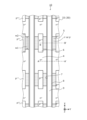
- FIG. 4 is a plan view showing the layout of the semiconductor device according to the embodiment viewed from the front surface side of the semiconductor substrate.
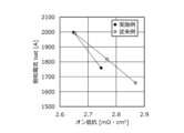
- FIG. 5 is a characteristic diagram showing the result of simulating the relationship between the on-resistance per unit area and the saturation current value in the example.
- FIG. 6 is a perspective view showing the structure of a conventional semiconductor device.
- FIG. 7 is a plan view showing a layout of a conventional semiconductor device viewed from the front surface side of the semiconductor substrate.
- n or p layers and regions prefixed with n or p mean that electrons or holes are majority carriers, respectively. Also, + and - attached to n and p mean that the impurity concentration is higher and lower than that of the layer or region not attached, respectively.
- the same configurations are denoted by the same reference numerals, and overlapping descriptions are omitted.
- FIG. 1 and 2 are cross-sectional views showing the structure of the semiconductor device according to the embodiment.
- FIG. 3 is a perspective view showing the structure of the semiconductor device according to the embodiment.
- FIG. 4 is a plan view showing the layout of the semiconductor device according to the embodiment viewed from the front surface side of the semiconductor substrate. 1 and 2 show cross-sectional structures taken along line AA' and line BB' of FIG. 4, respectively.
- FIG. 3 shows an enlarged view of the vicinity of the boundary between the n + -type source region 4, the low-concentration region 5 and the p ++ -type contact region 6 in FIG.
- FIG. 4 shows the layout of the n + -type source region 4, the low concentration region 5 (hatched portion) and the p ++ -type contact region 6. As shown in FIG.
- the semiconductor device 10 is a vertical MOSFET having a trench gate structure on the front surface side of a semiconductor substrate (semiconductor chip) 30 using silicon carbide (SiC) as a semiconductor material.
- the semiconductor substrate 30 includes an n ⁇ -type drift region (first semiconductor region) 2 and a p-type base region (second semiconductor region) 3 on the front surface of an n + -type starting substrate 31 using SiC as a semiconductor material. It is an epitaxial substrate formed by stacking epitaxial layers 32 and 33 in this order.
- the semiconductor substrate 30 has a front surface (first main surface) on the side of the epitaxial layer 33 that forms the p-type base region 3 , and a back surface (second main surface) on the side of the n + -type starting substrate 31 . and
- the n + -type starting substrate 31 is the n + -type drain region 1 .
- the n ⁇ -type drift region 2 adjoins the n + -type starting substrate 31 .
- P-type base region 3 is provided between the front surface of semiconductor substrate 30 and n ⁇ -type drift region 2 .
- the trench gate structure includes a p-type base region 3, an n + -type source region (third semiconductor region) 4, a low concentration region (fourth semiconductor region) 5, a p ++ -type contact region (fifth semiconductor region) 6, a trench 7 , a gate insulating film 8 and a gate electrode 9 .
- an n - type current diffusion region 23 and p + -type regions 21 and 22 are formed at a position deeper than the bottom of the trench 7 toward the n + -type drain region 1 side. They may be provided selectively.
- the n-type current diffusion region 23 and the p + -type regions 21 and 22 are diffusion regions formed inside the n - -type epitaxial layer 32 by ion implantation.
- a portion of n ⁇ -type epitaxial layer 32 excluding n-type current diffusion region 23 and p + -type regions 21 and 22 is n ⁇ -type drift region 2 .
- the n-type current spreading region 23 is a so-called current spreading layer (CSL) that reduces spreading resistance of carriers.
- N-type current diffusion region 23 is in contact with p-type base region 3 and n ⁇ -type drift region 2 in depth direction Z between trenches 7 adjacent to each other.
- the n-type current diffusion region 23 reaches the trench 7 in the direction parallel to the front surface of the semiconductor substrate 30 and contacts the gate insulating film 8 .
- a portion of the n-type current diffusion region 23 between the p + -type regions 21 and 22 adjacent to each other is a JFET region.
- the n ⁇ -type drift region 2 extends from the n + -type drain region 1 side to the p-type base region 3, and also extends from the semiconductor substrate 30. It reaches the trench 7 in the direction parallel to the front surface and contacts the gate insulating film 8 .
- a portion between the p + -type regions 21 and 22 adjacent to each other in the n ⁇ -type drift region 2 becomes a JFET region.
- the p + -type regions 21 and 22 are fixed to the potential of a source electrode (first electrode) 12, which will be described later, and are depleted (or the n-type current diffusion region 23 is depleted) when the MOSFET (semiconductor device 10) is turned off. or both), it has a function of relaxing the electric field applied to the gate insulating film 8 on the bottom surface of the trench 7 .
- the p + -type regions 21 and 22 each extend linearly along the trench 7 in a first direction X, which will be described later.
- the p + -type region 21 is provided apart from the p-type base region 3 and faces the bottom surface of the trench 7 in the depth direction Z. As shown in FIG.
- the p + -type region 21 may be in contact with the gate insulating film 8 at the bottom surface of the trench 7 or may be separated from the bottom surface of the trench 7 .
- the p + -type region 21 also faces the bottom corners (corners) of the trenches 7 in the depth direction Z.
- the bottom corner portion of the trench 7 is the boundary between the side wall of the trench 7 and the bottom surface.
- the p + -type regions 22 are provided between the trenches 7 adjacent to each other, separated from the trenches 7 and the p + -type regions 21 .
- the p + -type region 22 is in contact with the p-type base region 3 on the surface on the n + -type source region 4 side, and is electrically connected to the source electrode 12 via the p-type base region 3 .
- the p + -type region 22 faces the p ++ -type contact region 6 in the depth direction Z.
- the width of the p + -type region 22 (the width in the second direction Y) is about equal to or greater than the width of the p ++ -type contact region 6 (the width in the second direction Y).
- the trench 7 penetrates the epitaxial layer 33 from the front surface of the semiconductor substrate 30 in the depth direction Z to form an n-type current diffusion region 23 (n - type drift region 2 when the n-type current diffusion region 23 is not provided). and terminates inside the n-type current spreading region 23 or inside the p + -type region 21 .
- the trenches 7 are arranged in stripes extending in a first direction X (vertical direction in FIG. 4) parallel to the front surface of the semiconductor substrate 30 . Between the trenches 7 adjacent to each other, between the front surface of the semiconductor substrate 30 and the p-type base region 3, the n + -type source region 4, the low-concentration region 5 and the p ++- type contact region 6 are selectively formed. is provided in
- Epitaxial layer 33 is either an n ⁇ -type epitaxial layer or a p ⁇ -type epitaxial layer having a p - type impurity concentration lower than that of p-type base region 3 .
- the p-type base region 3, the n + -type source region 4 and the p ++- type contact region 6 are diffusion regions formed inside the epitaxial layer 33 by ion implantation.
- the low-concentration region 5 is a surface region of the epitaxial layer 33 (the surface region of the front surface of the semiconductor substrate 30) that is left without forming the n + -type source region 4 and the p ++ -type contact region 6. This is the part that was
- the epitaxial layer 33 is an n ⁇ -type epitaxial layer having an n - type impurity concentration similar to that of the n ⁇ -type drift region 2, or, for example, 1 ⁇ 10 15 /cm 3 or more and 1 ⁇ 10 It is a p ⁇ -type epitaxial layer with a p-type impurity concentration of about 16 /cm 3 or less.
- a p-type region constituting a breakdown voltage structure can be formed in the surface region of the epitaxial layer 33 by ion implantation in an edge termination region (not shown) surrounding the active region.
- the p ⁇ -type epitaxial layer 33 it is possible to shorten the ion implantation time for forming the p-type base region 3 and reduce the ion implantation dose.
- the p ⁇ -type epitaxial layer 33 in the edge termination region is removed to expose the underlying n ⁇ -type epitaxial layer 32, and the exposed surface of the n ⁇ -type epitaxial layer 32 is exposed.
- a p-type region forming a breakdown voltage structure may be formed by ion implantation.
- the active region is a region in which MOSFET unit cells (components of an element) are arranged and a main current (drift current) flows.
- the active region is arranged substantially in the center of the semiconductor substrate 30, for example. Although only one unit cell of the MOSFET is illustrated in FIGS. 1 and 2, a plurality of unit cells having the same structure are arranged adjacent to each other in the active region of the semiconductor substrate 30.
- the edge termination region is a region between the active region and the chip edge (the edge of the semiconductor substrate 30), surrounds the active region, relaxes the electric field on the front surface side of the semiconductor substrate 30, and withstands the breakdown voltage. hold.
- the breakdown voltage is the limit voltage at which avalanche breakdown occurs in the pn junction and the drain-source voltage does not increase even if the drain-source current is increased.
- a general breakdown voltage structure such as a Junction Termination Extension (JTE) structure or a Field Limiting Ring (FLR) structure is arranged.
- the p-type base region 3 is formed by ion implantation of p-type impurities such as aluminum (Al) from the surface of the epitaxial layer 33 (the front surface of the semiconductor substrate 30). This ion implantation adjusts the resistance of a channel (n-type inversion layer) formed in a portion (hereinafter referred to as a channel portion) 3a along the trench 7 of the p-type base region 3 when the MOSFET is turned on.
- the p-type base region 3 has a peak impurity concentration (maximum concentration) at the center in the depth direction Z, and from the depth position of the peak concentration toward the front surface side and the back surface side of the semiconductor substrate 30, respectively. The impurity concentration distribution is such that the impurity concentration is low.
- a channel portion 3 a of the p-type base region 3 has substantially the same length as the length of the trench 7 in the longitudinal direction (first direction X) and extends linearly in the first direction X along the side wall of the trench 7 .
- a p-type epitaxial layer 33 having an impurity concentration substantially equal to that of the p-type base region 3 may be formed, and ion implantation may be performed only in the channel portion 3a of the p-type base region 3 for adjusting the channel resistance value. good.
- the p-type base region 3 has a peak impurity concentration at the center of the depth direction Z only in the channel portion 3a, and the depth position of the peak concentration reaches the front surface side and the back surface side of the semiconductor substrate 30.
- the impurity concentration distribution is such that the impurity concentration becomes lower as it goes to each direction, and the impurity concentration distribution is uniform in the depth direction Z in the remaining portion of the p-type epitaxial layer 33 without ion implantation.
- Approximately the same impurity concentration and approximately the same length mean the same impurity concentration and the same length within a range including tolerance due to process variations.
- the n + -type source region 4 , the low concentration region 5 and the p ++ -type contact region 6 are exposed on the front surface of the semiconductor substrate 30 . Being exposed on the front surface of the semiconductor substrate 30 means that the front surface of the semiconductor substrate 30 is in contact with the source electrode 12 described later.
- the n + -type source region 4 and the low-concentration region 5 are in contact with the gate insulating film 8 on the sidewalls of the trench 7 and adjacent to the channel portion 3a of the p-type base region 3 in the depth direction Z.
- the n + -type source regions 4 and the low-concentration regions 5 are alternately and repeatedly arranged adjacent to each other in the first direction X. As shown in FIG.
- the p ++ -type contact region 6 is provided in contact with the n + -type source region 4 at a position away from the trench 7 .
- the n + -type source regions 4 and the p ++ -type contact regions 6 are alternately and repeatedly arranged adjacent to each other in the first direction X. As shown in FIG.
- Low concentration region 5 is preferably arranged only between trench 7 and p ++ -type contact region 6 . That is, the low-concentration region 5 and the p ++ -type contact region 6 are preferably adjacent to each other in the second direction Y parallel to the front surface of the semiconductor substrate 30 and perpendicular to the first direction X. As shown in FIG.
- the n + -type source region 4 between the low concentration regions 5 adjacent to each other in the first direction X and the first is because the n + -type source regions 4 between the p ++ -type contact regions 6 that are adjacent to each other in the direction X are separated, resulting in a complicated pattern, which may make it difficult to form the n + -type source regions 4 . .
- the p ++ -type contact region 6 is located between the adjacent trenches 7 in the first direction.
- the low-concentration regions 5 are arranged between the trenches 7 and the p ++ -type contact regions 6 and are scattered in the first direction X. As shown in FIG.
- n + -type source regions 4 between the low concentration regions 5 adjacent to each other in the first direction X and the n + -type source regions 4 between the p ++ -type contact regions 6 adjacent to each other in the first direction X are the second They are connected in the direction Y and form a substantially rectangular planar shape with a relatively large surface area.
- the low concentration region 5 and the p ++ type contact region 6 may be in contact with each other.
- the width w1 of the low-concentration region 5 in the first direction X is less than or equal to the width w2 of the p ++ -type contact region 6 in the first direction X. Therefore, the n + -type source region 4 is a substantially rectangular region contacting the low-concentration region 5 and the p ++ -type contact region 6 in the first direction X and the gate insulating film 8 on the side wall of the trench 7 in the second direction Y. It forms a planar shape of the shape.
- the n + -type source region 4 extends in the first direction X in contact with the gate insulating film 8 on the side wall of the trench 7 , and the end in the first direction X is located between the trench 7 and the p ++ -type contact region 6 . It has a substantially H-shaped planar shape having a linear portion terminating between the two and a portion sandwiched between the p ++ -type contact regions 6 adjacent to each other in the first direction X. As shown in FIG.
- the width w1 of the low-concentration region 5 in the first direction X is preferably within a range of, for example, approximately 1.0 ⁇ m or more and 4.0 ⁇ m or less.
- the width w1 of the low-concentration region 5 in the first direction X corresponds to the length of the low-concentration region 5 in contact with the gate insulating film 8 on the side wall of the trench 7 in the first direction X.
- the width w1 of the low-concentration region 5 in the first direction X is less than the above lower limit, there is a possibility that the effect of providing the low-concentration region 5 may not be obtained, which is not preferable.
- the width w1 in the first direction X of the low-concentration region 5 exceeds the above upper limit, the current path of the drift current becomes high resistance when the MOSFET is turned on, and the on-resistance increases, which is not preferable.
- a p-type impurity is introduced into the low concentration region 5 by ion implantation of the p-type impurity for forming the p-type base region 3 (or for adjusting the channel resistance value).
- the ion implantation is performed such that the impurity concentration is increased from the surface of the epitaxial layer 33 (the front surface of the semiconductor substrate 30) to the center depth position (range) in the depth direction Z of the channel portion 3a of the p-type base region 3. It is carried out under the conditions of maximum (peak concentration). Therefore, in the low-concentration region 5, the impurity concentration becomes maximum (peak concentration) at a predetermined depth position, and the impurity concentration becomes lower along the depth direction Z from the depth position where the peak concentration is obtained.
- the low concentration region 5 is an n ⁇ type region (first conductivity type region) having a lower n type impurity concentration than the n + type source region 4 .
- the n ⁇ -type low-concentration region 5 has the highest impurity concentration near the front surface of the semiconductor substrate 30, and the impurity concentration decreases toward the back surface side (n + -type drain region 1 side) of the semiconductor substrate 30. It has an n-type impurity concentration distribution (first conductivity type impurity concentration distribution).
- the n - type impurity concentration of the n ⁇ -type low concentration region 5 is adjusted to the n-type during the epitaxial growth of the n ⁇ -type epitaxial layer 33 by introducing the p-type impurity into the low concentration region 5 during the formation of the p-type base region 3 . It is slightly lower than the impurity concentration.
- the n - type impurity concentration of the n ⁇ -type low-concentration region 5 is set, for example, within a range of approximately 1 ⁇ 10 14 /cm 3 to 1 ⁇ 10 18 /cm 3 .
- the low concentration region 5 is a p ⁇ type region (second conductivity type region) having a lower p type impurity concentration than the channel portion 3 a of the p type base region 3 .
- the p ⁇ -type low-concentration region 5 has the lowest impurity concentration near the front surface of the semiconductor substrate 30 and has a p-type impurity concentration distribution (second conductive region) in which the impurity concentration increases toward the back surface side of the semiconductor substrate 30 . type impurity concentration distribution).
- the p - type impurity concentration of the p ⁇ -type low concentration region 5 is reduced to the p-type during epitaxial growth of the p ⁇ -type epitaxial layer 33 by introducing the p-type impurity into the low concentration region 5 during the formation of the p-type base region 3 . It is slightly higher than the impurity concentration.
- the p - type impurity concentration of the p ⁇ -type low-concentration region 5 is set, for example, within a range of approximately 1 ⁇ 10 14 /cm 3 to 1 ⁇ 10 18 /cm 3 .
- the surface region of the low concentration region 5 is reduced when the MOSFET is turned on. Low resistance.
- the surface region of the low-concentration region 5 is inverted to the n-type when the MOSFET is turned on, resulting in low resistance.
- a drift current flows from the n + type source region 4 to the low-resistance surface region of the lightly doped region 5 when the MOSFET is turned on. Since the area through which the drift current flows from the front surface of the semiconductor substrate 30 to the source electrode 12 increases, the on-resistance can be reduced.
- a gate insulating film 8 is provided inside the trench 7 along the inner wall of the trench 7 , and a gate electrode 9 is provided on the gate insulating film 8 .
- the gate insulating film 8 includes the n + -type source region 4, the low concentration region 5, the p-type base region 3, and the n-type current diffusion region 23 (n ⁇ -type when the n-type current diffusion region 23 is not provided) on the inner wall of the trench 7. It touches the drift region 2).
- the trench gate structure includes, on the side wall of the trench 7, a portion where the gate insulating film 8 is in contact with the n + -type source region 4, the p-type base region 3 and the n-type current diffusion region 23, the gate insulating film 8 is provided with the low concentration region 5, The portions where the p-type base regions 3 and the n-type current diffusion regions 23 are in contact with each other are alternately repeated in the first direction X and are periodically arranged adjacent to each other.
- the interlayer insulating film 11 is provided over the entire front surface of the semiconductor substrate 30 and covers the gate electrode 9 .
- a contact hole in the interlayer insulating film 11 exposes the n + -type source region 4 , the low-concentration region 5 and the p ++ -type contact region 6 .
- the source electrode 12 is in contact with the n + -type source region 4 , the low-concentration region 5 and the p ++ -type contact region 6 in the contact hole of the interlayer insulating film 11 .
- a drain (second electrode) electrode 13 is provided on the entire back surface of the semiconductor substrate 30 (the back surface of the n + -type starting substrate 31). The drain electrode 13 is in contact with the n + -type drain region 1 (n + -type starting substrate 31 ) and electrically connected to the n + -type drain region 1 .
- the operation of the semiconductor device 10 will be described.
- a gate-source voltage equal to or higher than the gate threshold voltage is applied to the gate electrode 9 while a positive voltage (forward voltage) is applied to the drain electrode 13 with respect to the source electrode 12, the p-type base region 3 A channel (n-type inversion layer) is formed in a portion (channel portion 3a) along the side wall of trench 7 of .
- a drift current flows from the drain electrode 13 toward the source electrode 12 through the n + type drain region 1, the n ⁇ type drift region 2, the n type current diffusion region 23, the channel and the n + type source region 4,
- the MOSFET semiconductor device 10.
- the drift current flows from the channel only to the n + -type source region 4. , and does not flow from the channel into the low concentration region 5 . Therefore, the drift current that has flowed into the channel immediately below the low concentration region 5 flows along the interface between the channel and the low concentration region 5 and into the n + -type source region 4 in the direction parallel to the front surface of the semiconductor substrate 30 . flow towards. Therefore, the current path of the drift current is lengthened by the distance that the drift current flows in the channel from immediately below the low concentration region 5 toward the n + -type source region 4, resulting in high resistance.
- the channel is pinched off at a lower drain-source voltage than in the conventional structure without the low concentration region 5 (see FIGS. 6 and 7). That is, the low concentration region 5 can reduce the pinch-off voltage of the channel. As a result, it is possible to shorten the time until the drain-source current (short-circuit current) that flows when the load or arm is short-circuited is shut off, and the saturation current value can be reduced, thereby improving the short-circuit resistance. be able to.
- the saturation current value is the saturation value of the drain-source current determined depending on the gate-source voltage.
- the ohmic contact area with the source electrode 12 is reduced by the contact area between the source electrode 12 and the low-concentration region 5, compared with the conventional structure in which the low-concentration region 5 is not provided.
- the on-resistance per unit increases, but the effect of reducing the saturation current value increases. This makes it possible to improve the trade-off relationship between the reduction in on-resistance and the reduction in saturation current value (see FIG. 5 described later).
- the impurity concentration of the low concentration region 5 to be low within the range described above, the increase in on-resistance due to the provision of the low concentration region 5 does not adversely affect the electrical characteristics of the MOSFET.
- the n-type impurity concentration in the surface region (the portion on the front surface side of the semiconductor substrate 30) is relatively high, or the p ⁇ -type low concentration region 5
- the low-concentration region 5 has a relatively low resistance in the surface region when the MOSFET is turned on.
- the drift current flows from the n + -type source region 4 to the relatively low-resistance surface region of the low-concentration region 5 , and the area of the current path of the drift current flowing from the semiconductor substrate 30 to the source electrode 12 is equal to that of the semiconductor substrate 30 . Since it becomes larger at the junction surface of the source electrode 12, the on-resistance can be reduced.
- an n + -type starting substrate (n + -type starting wafer) 31 using silicon carbide as a semiconductor material is prepared.
- an n ⁇ -type epitaxial layer 32 to be the n ⁇ -type drift region 2 is epitaxially grown (deposited) on the front surface of the n + -type starting substrate 31 .
- photolithography and ion implantation of p - type impurities p + -type regions 21 and p + -type regions 21 and p A lower portion of the + type region 22 (portion on the n + type drain region 1 side) is selectively formed.
- n - type current diffusion region 23 is formed between p + -type region 21 and p + -type region 22 adjacent to each other in the surface region of n ⁇ -type epitaxial layer 32 .
- the order of formation of the p + -type region 21, the bottom of the p + -type region 22, and the bottom of the n-type current diffusion region 23 can be changed as appropriate.
- epitaxial growth is further performed to thicken the n ⁇ -type epitaxial layer 32 to a predetermined thickness.
- the thickened portion of the n ⁇ -type epitaxial layer 32 is connected to the bottom of the p + -type region 22 in the depth direction Z.
- An upper portion of the p + -type region 22 portion on the n + -type source region 4 side is selectively formed.
- an n-type impurity is formed in the thickened portion of the n ⁇ -type epitaxial layer 32 so as to face and connect to the lower portion of the n-type current diffusion region 23 in the depth direction Z.
- An upper portion of the current spreading region 23 is formed. The order of forming the upper portion of the p + -type region 22 and the upper portion of the n-type current diffusion region 23 can be changed as appropriate.
- an n ⁇ -type or p ⁇ -type epitaxial layer 33 to be the p-type base region 3 is epitaxially grown (deposited).
- a semiconductor substrate (semiconductor wafer) 30 is produced (manufactured) in which epitaxial layers 32 and 33 are sequentially laminated on the front surface of the n + -type starting substrate 31 .
- a p-type impurity such as aluminum is ion-implanted into the epitaxial layer 33 so that the central depth position in the depth direction Z of the portion left as the p-type base region 3 has a peak concentration of the impurity concentration.
- the mold base region 3 is formed and the channel resistance value of the channel portion 3a is adjusted.
- an n + -type source region 4 is selectively formed in the surface region of the epitaxial layer 33 by photolithography and ion-implantation of n-type impurities, and a p ++ -type contact region is formed by photolithography and ion-implantation of p-type impurities. 6 is selectively formed.
- the conductivity type (n ⁇ type or p ⁇ type) of the epitaxial layer 33 is changed without forming the n + type source region 4 and the p ++ type contact region 6 in the portion of the surface region of the epitaxial layer 33 to be the low concentration region 5 . Leave as is.
- a portion of the epitaxial layer 33 closer to the n ⁇ -type epitaxial layer 32 than the n + -type source region 4 , the low-concentration region 5 and the p ++ -type contact region 6 serves as the p-type base region 3 .
- a p-type region forming a breakdown voltage structure is selectively formed in the surface region of 32 .
- the order of forming the n + -type source region 4, the p ++ -type contact region 6, and the p-type region forming the breakdown voltage structure can be changed as appropriate.
- heat treatment is performed to activate all the ion-implanted impurities. This heat treatment for impurity activation may be performed each time ion implantation is performed.
- the semiconductor substrate 30 extends from the front surface (surface of the epitaxial layer 33) of the semiconductor substrate 30 through the n + -type source region 4, the low-concentration region 5 and the p-type base region 3 in the depth direction Z. to form a trench 7 reaching the n-type current diffusion region 23 and terminating inside the n-type current diffusion region 23 .
- a gate insulating film 8, a gate electrode 9, an interlayer insulating film 11, a source electrode 12 and a drain electrode 13 are formed by a general method.
- the semiconductor wafer semiconductor substrate 30
- an n-type source region having an impurity concentration lower than that of the n + -type source region is formed.
- a ⁇ type low concentration region is provided, or a p ⁇ type low concentration region having a lower p type impurity concentration than the channel portion of the p type base region is provided.
- This low concentration region can reduce the pinch-off voltage of the channel. As a result, it is possible to shorten the time until the drain-source current (short-circuit current) that flows when the load or arm is short-circuited is shut off, and the saturation current value can be reduced, thereby improving the short-circuit resistance. be able to.
- the portion of the surface region of the n ⁇ type or p ⁇ type epitaxial layer, which is to be the low concentration region, is formed without forming the n + type source region and the p ++ type contact region.
- the conductivity type (n ⁇ type or p ⁇ type) of 1 As it is, an n ⁇ type or p ⁇ type low concentration region can be formed. Therefore, by appropriately changing the ion implantation mask patterns for forming the n + -type source region and the p ++ -type contact region, the conventional method of manufacturing a semiconductor device (see FIGS. 6 and 7) can be used. can be used to form a low-concentration region. Therefore, the short-circuit resistance can be improved without increasing the number of steps.
- the contact area between the source electrode and the low concentration region is reduced by providing the low concentration region instead of part of the n + -type source region in the surface region of the front surface of the semiconductor substrate.
- the ohmic contact area with the source electrode is reduced accordingly, and the on-resistance per unit area is increased, but the effect of reducing the saturation current value is increased. This makes it possible to improve the trade-off relationship between reduction in on-resistance and reduction in saturation current value.
- the impurity concentration of the low-concentration region to be low within the range described above, the increase in on-resistance caused by providing the low-concentration region does not adversely affect the electrical characteristics of the MOSFET.
- the n-type impurity concentration in the surface region (the portion on the front surface side of the semiconductor substrate) is relatively high, or The p-type impurity concentration of the surface region is made relatively low in the low concentration region.
- the MOSFET when the MOSFET is turned on, the low-concentration region has a relatively low resistance in the surface region, and a drift current flows from the n + -type source region to the relatively low-resistance surface region of the low-concentration region.
- the area of the current path of the drift current flowing from the semiconductor substrate to the source electrode is increased at the junction surface between the semiconductor substrate and the source electrode, so that the on-resistance can be reduced.
- the low-concentration regions can be formed.
- a low-concentration region can be formed by designing the conditions of the dimensions (first direction and second direction).
- the thickness of the channel portion of the p-type base region, the thickness of the epitaxial layer that becomes the p-type base region, and the three-dimensional (first direction, second direction, and depth direction) such as ion implantation conditions for the channel portion can be obtained. There is no need to consider design conditions by combining multiple conditions. Therefore, a semiconductor device with high short-circuit resistance can be manufactured at low cost.
- FIG. 5 is a characteristic diagram showing the result of simulating the relationship between the on-resistance per unit area and the saturation current value in the example.
- the horizontal axis of FIG. 5 is the on-resistance [m ⁇ cm 2 ] per unit area, and the vertical axis is the saturation value of the saturation current Isat (saturation current value) [A].
- FIG. 5 shows the results of simulating the saturation current value with respect to the on-resistance per unit area for each of the embodiment and the conventional example (conventional semiconductor device 110 shown in FIGS. 6 and 7).
- the conventional example differs from the embodiment in that the low-concentration region 5 is not provided.
- the on-resistance per unit area is changed by changing the impurity concentration of the channel portions 3a and 103a of the p-type base regions 3 and 103 to change the channel resistance value.
- the embodiment can improve the trade-off relationship between the reduction of the on-resistance and the reduction of the saturation current value compared to the conventional example.
- the saturation current value decreases at a predetermined ratio as the on-resistance increases.
- the present invention is not limited to the above-described embodiment, and various modifications can be made without departing from the scope of the present invention.
- the present invention can also be applied to a semiconductor device using silicon (Si) as a semiconductor material.
- the present invention has been described assuming that the first conductivity type is n-type and the second conductivity type is p-type. similarly established.
- the semiconductor device according to the present invention is useful as a power semiconductor device used in power converters and power supply devices for various industrial machines, and is particularly useful for MOSFETs using silicon carbide as a semiconductor material. Are suitable.
Abstract
n+型ソース領域(4)、低濃度領域(5)およびp++型コンタクト領域(6)は、半導体基板(30)のおもて面の表面領域にそれぞれ選択的に設けられ、ソース電極に接する。n+型ソース領域(4)および低濃度領域(5)は、トレンチ(7)の側壁でゲート絶縁膜(8)に接し、深さ方向(Z)にp型ベース領域のチャネル部分に隣接する。p++型コンタクト領域(6)は、トレンチ(7)から離れて配置される。p型ベース領域となるエピタキシャル層(33)の表面領域のうち、n+型ソース領域(4)およびp++型コンタクト領域(6)を形成せずに残された部分で、n-型またはp-型の低濃度領域(5)が構成される。低濃度領域(5)は、p++型コンタクト領域(6)とトレンチ(7)との間に、トレンチ(7)の側壁に沿って周期的に配置される。このような構造とすることで、工程数を増やすことなく、短絡耐量を大きくすることができる。
Description
この発明は、半導体装置に関する。
従来、MOSFET(Metal Oxide Semiconductor Field Effect Transistor:金属-酸化膜-半導体の3層構造からなる絶縁ゲートを備えたMOS型電界効果トランジスタ)では、短絡電流を抑制するため、飽和電流値が小さくなるように最適設計がなされる。短絡電流とは、負荷短絡時やアーム短絡時に流れるドレイン・ソース間電流であり、定格電流を超える大電流となる。飽和電流値とは、ゲート・ソース間電圧に依存して決まるドレイン・ソース間電流の飽和値である。
一般的に、p型ベース領域のチャネル(n型の反転層)が形成される部分に、p型ベース領域よりもp型不純物濃度の低いp-型低濃度領域を配置してチャネルをピンチオフしやすくすることで、ドレイン・ソース間電流が遮断されるまでの時間を短くし、飽和電流値を小さく設定している。また、オン状態のときにドレイン・ソース間に流れるドリフト電流の電流経路にチャネルに隣接して形成されるn型のJFET(Junction FET)領域の形状や不純物濃度勾配を利用して、飽和電流値を小さく設定している。
JFET領域の形状を利用するとは、JFET領域の幅(ドリフト電流の電流経路の一部の幅)が狭くなるようにJFET領域の幅を決めるp+型領域の配置を適宜設定したりすることである。JFET領域の不純物濃度勾配を利用するとは、チャネルのp型不純物濃度に対してJFET領域のn型不純物濃度を低く設定することである。JFET領域を最適設計することで、ソース電極に対して正の電圧(順方向電圧)がドレイン電極に印加されたときにJFET領域が空乏化されやすくなるため、飽和電流値が小さくなる。
従来のMOSFETの構造について、炭化珪素(SiC)を半導体材料として用いたトレンチゲート構造の縦型MOSFETを例に説明する。図6は、従来の半導体装置の構造を示す斜視図である。図6には、図7のn+型ソース領域104とp++型コンタクト領域106との境界付近を拡大して示す。図7は、従来の半導体装置を半導体基板のおもて面側から見たレイアウトを示す平面図である。図7には、n+型ソース領域104およびp++型コンタクト領域106のレイアウトを示す。
図6,7に示す従来の半導体装置110は、炭化珪素からなる半導体基板130のおもて面側にトレンチゲート構造を備えた縦型MOSFETである。半導体基板130は、n-型ドリフト領域102およびp型ベース領域103となる各エピタキシャル層を含み、p型ベース領域103となるp型エピタキシャル層側の主面をおもて面とする。トレンチゲート構造は、p型ベース領域103、n+型ソース領域104、p++型コンタクト領域106、トレンチ107、ゲート絶縁膜108およびゲート電極109で構成される。
トレンチ107は、半導体基板130のおもて面に平行な第1方向X(図7の縦方向)に延在するストライプ状に配置されている。n+型ソース領域104およびp++型コンタクト領域106は、半導体基板130のおもて面とp型ベース領域103との間にそれぞれ選択的に設けられている。n+型ソース領域104は、トレンチ107の側壁のゲート絶縁膜108に接する。p++型コンタクト領域106は、トレンチ107から離れた位置に、n+型ソース領域104に接して設けられている。
互いに隣り合うトレンチ107間において、p++型コンタクト領域106は第1方向Xに点在し、n+型ソース領域104はp++型コンタクト領域106の周囲を囲む梯子状の平面形状をなす。n+型ソース領域104とp++型コンタクト領域106とは、第1方向Xに交互に繰り返し隣接して配置されている。n+型ソース領域104は、トレンチ107の側壁のゲート絶縁膜108に接して第1方向Xに直線状に延在する部分と、第1方向Xに互いに隣り合うp++型コンタクト領域106間に挟まれた部分と、を有する。
したがって、トレンチゲート構造は、トレンチ107の側壁の全域にわたって、n+型ソース領域104、p型ベース領域103およびn型電流拡散領域123がゲート絶縁膜108に接して第1方向Xに延在した構造となっている。n+型ソース領域104およびp++型コンタクト領域106は、それぞれ半導体基板130のおもて面の表面領域にイオン注入により選択的に形成された拡散領域である。p+型領域121,122は、トレンチ107の底面よりもn+型ドレイン領域(不図示)側に深い位置に配置されている。符号111は層間絶縁膜である。
従来のトレンチゲート構造の縦型MOSFETとして、ソース領域を、ソース電極に接するn+型ソース領域と、n+型ソース領域とp型ベース領域との間のn型ソース領域と、で構成した装置が提案されている(例えば、下記特許文献1参照。)。下記特許文献1では、ソース領域のうちの相対的に不純物濃度の低いn型ソース領域に広範囲に入り込むように空乏化を生じさせ、ドリフト電流を流れにくくすることで、負荷短絡時の飽和電流値を小さくして、短絡耐量を向上させている。
また、従来のトレンチゲート構造の別の縦型MOSFETとして、n+型ソース領域およびp+型コンタクト領域とトレンチとの間にp型ベース領域の一部を配置し、これらの領域とp型ベース領域の残りの部分に形成されるチャネルとの間にn型シャント抵抗領域を配置した装置が提案されている(例えば、下記特許文献2参照。)。下記特許文献2では、定格電流を超えるドリフト電流が流れる異常時に、定格電流時よりもn型シャント抵抗領域の抵抗値分だけオン抵抗を高くすることで、短絡耐量を向上させている。
また、従来のトレンチゲート構造の別の縦型MOSFETとして、n型ソース領域を、深さ方向にチャネルに対向する部分のみリン(P)のイオン注入で形成し、残りの部分をヒ素(As)のイオン注入で形成した装置が提案されている(例えば、下記特許文献3参照。)。下記特許文献3では、ヒ素よりも飛程が大きく深い位置に達するリンによって、n型ソース領域を深さ方向にチャネルに対向する部分で相対的に深くすることで、チャネル長を短縮化し、素子特性を向上させている。
また、従来のプレーナゲート構造の縦型MOSFETとして、p型ベース領域とn-型ドリフト領域との間に、p型ベース領域よりもJFET領域から離れて、n-型ドリフト領域よりも不純物濃度の低いn-型低濃度領域を備えた装置が提案されている(例えば、下記特許文献4参照。)。下記特許文献4では、短絡時にn-型ドリフト領域に広がる空乏層をn-型低濃度領域によって変形させ、ドリフト電流の電流経路上での局所的な電界集中を防止して、局所的な発熱を抑制することで、短絡耐量を向上させている。
また、従来のトレンチゲート構造の別の縦型MOSFETとして、n型ソース領域を、トレンチ側で相対的に不純物濃度を低くし、トレンチから離れた部分で相対的に不純物濃度を高くした装置が提案されている(例えば、下記特許文献5参照。)。下記特許文献5では、ソース領域の相対的に不純物濃度を低くした部分でゲート絶縁膜のリーク電流密度を低く抑え、相対的に不純物濃度を高くした部分でソース電極との良好なコンタクト(電気接触部)を形成している。
また、従来のプレーナゲート構造の別の縦型MOSFETとして、半導体基板のおもて面の表面領域においてn+型ソース領域とJFET領域との間のチャネルとして機能する部分を、p型ベース領域よりもp型不純物濃度を低くし、かつp型ベース領域よりもp型不純物に対するn型不純物の比率を大きくした装置が提案されている(例えば、下記特許文献6参照。)。下記特許文献6では、n+型ソース領域とJFET領域との間のチャネルとして機能する部分でゲート閾値電圧を調整し、電子の移動度を向上させている。
しかしながら、従来の半導体装置110(図6,7参照)では、飽和電流値を小さく設定する場合、トレンチゲート構造であることで次の問題が生じる。上述したようにp型ベース領域のチャネルが形成される部分にp-型低濃度領域を配置することで飽和電流値を小さく設定する場合、p型ベース領域103のチャネルが形成される部分103aにp-型低濃度領域(不図示)を形成するためのエピタキシャル成長工程やイオン注入工程を追加する必要がある。このため、工程数が多くなり、コスト増大につながる。
上述したようにJFET領域(互いに隣り合うp+型領域121,122間の部分)の形状や不純物濃度勾配を利用して飽和電流値を小さく設定する場合、オン抵抗が急激に増加して、電気的特性が犠牲になる。また、トレンチ107の底面よりもn+型ドレイン領域(不図示)側に深い部分に、所定の飽和電流値が得られるように特殊な形状でp+型領域121,122を形成するため、工程が複雑になったり、高加速エネルギーでイオン注入可能な高価なイオン注入装置を準備したりする必要があり、コスト増大につながる。
この発明は、上述した従来技術による課題を解消するため、工程数を増加させることなく、短絡耐量を向上させることができる半導体装置を提供することを目的とする。
上述した課題を解決し、本発明の目的を達成するため、この発明にかかる半導体装置は、次の特徴を有する。半導体基板の内部に、第1導電型の第1半導体領域が設けられている。前記半導体基板の第1主面と前記第1半導体領域との間に、第2導電型の第2半導体領域が設けられている。トレンチは、深さ方向に前記半導体基板の第1主面から前記第2半導体領域を貫通して、前記第1半導体領域の内部で終端する。前記トレンチの内部に、ゲート絶縁膜を介してゲート電極が設けられている。前記半導体基板の第1主面と前記第2半導体領域との間に、第1導電型の第3半導体領域が選択的に設けられている。前記第3半導体領域は、前記トレンチの側壁の前記ゲート絶縁膜に接する。前記半導体基板の第1主面と前記第2半導体領域との間に、第4半導体領域が選択的に設けられている。
前記第4半導体領域は、前記トレンチの側壁の前記ゲート絶縁膜に接する。前記半導体基板の第1主面と前記第2半導体領域との間に、前記トレンチから離れて、第2導電型の第5半導体領域が選択的に設けられている。前記第5半導体領域は、前記第2半導体領域よりも不純物濃度が高い。第1電極は、前記第3半導体領域、前記第4半導体領域および前記第5半導体領域に接する。第2電極は、前記半導体基板の第2主面に接する。前記第4半導体領域は、前記第3半導体領域よりも第1導電型不純物濃度の低い第1導電型領域であるか、または前記第2半導体領域の、前記トレンチの側壁に沿った部分よりも第2導電型不純物濃度の低い第2導電型領域である。
また、この発明にかかる半導体装置は、上述した発明において、前記第4半導体領域は、前記半導体基板の第1主面に平行な方向に前記トレンチの側壁に沿って周期的に配置されていることを特徴とする。
また、この発明にかかる半導体装置は、上述した発明において、前記第4半導体領域は、前記第5半導体領域と前記トレンチとの間に配置されていることを特徴とする。
また、この発明にかかる半導体装置は、上述した発明において、前記第4半導体領域の不純物濃度は、1×10¹⁴/cm3以上1×1018/cm3以下の範囲内であることを特徴とする。
また、この発明にかかる半導体装置は、上述した発明において、前記第4半導体領域は、前記第1導電型領域であり、前記半導体基板の第1主面で最も不純物濃度が高く、前記半導体基板の第2主面側へ向かうにしたがって不純物濃度が低くなる第1導電型不純物濃度分布を有することを特徴とする。
また、この発明にかかる半導体装置は、上述した発明において、前記第4半導体領域は、前記第2導電型領域であり、前記半導体基板の第1主面で最も不純物濃度が低く、前記半導体基板の第2主面側へ向かうにしたがって不純物濃度が高くなる第2導電型不純物濃度分布を有することを特徴とする。
また、この発明にかかる半導体装置は、上述した発明において、前記第4半導体領域は、前記半導体基板の第1主面に平行な方向に前記トレンチの側壁の前記ゲート絶縁膜に1.0μm以上4.0μm以下の範囲内の長さで接していることを特徴とする。
また、この発明にかかる半導体装置は、上述した発明において、前記トレンチは、前記半導体基板の第1主面に平行な第1方向に延在するストライプ状に配置されている。前記第3半導体領域と前記第4半導体領域とは前記第1方向に交互に繰り返し配置されている。前記第3半導体領域と前記第5半導体領域とは前記第1方向に交互に繰り返し配置されていることを特徴とする。
また、この発明にかかる半導体装置は、上述した発明において、前記第4半導体領域の前記第1方向の幅は、前記第5半導体領域の前記第1方向の幅以下であることを特徴とする。
また、この発明にかかる半導体装置は、上述した発明において、炭化珪素からなる前記半導体基板を用いたことを特徴とする。
上述した発明によれば、第4半導体領域によってチャネルのピンチオフ電圧を低減させることができるため、負荷短絡時やアーム短絡時に流れる短絡電流が遮断されるまでの時間を短くすることができ、飽和電流値を小さくすることができる。また、上述した発明によれば、第3半導体領域および第5半導体領域をそれぞれ形成するためのイオン注入用マスクパターンを適宜変更することで、従来の半導体装置(図6,7参照)の製造方法を利用して第4半導体領域を形成することができる。
本発明にかかる半導体装置によれば、工程数を増加させることなく、短絡耐量を向上させることができるという効果を奏する。
以下に添付図面を参照して、この発明にかかる半導体装置の好適な実施の形態を詳細に説明する。本明細書および添付図面においては、nまたはpを冠記した層や領域では、それぞれ電子または正孔が多数キャリアであることを意味する。また、nやpに付す+および-は、それぞれそれが付されていない層や領域よりも高不純物濃度および低不純物濃度であることを意味する。なお、以下の実施の形態の説明および添付図面において、同様の構成には同一の符号を付し、重複する説明を省略する。
(実施の形態)
実施の形態にかかる半導体装置の構造について説明する。図1,2は、実施の形態にかかる半導体装置の構造を示す断面図である。図3は、実施の形態にかかる半導体装置の構造を示す斜視図である。図4は、実施の形態にかかる半導体装置を半導体基板のおもて面側から見たレイアウトを示す平面図である。図1,2には、それぞれ図4の切断線A-A’および切断線B-B’における断面構造を示す。図3には、図4のn+型ソース領域4と低濃度領域5とp++型コンタクト領域6との境界付近を拡大して示す。図4には、n+型ソース領域4、低濃度領域5(ハッチング部分)およびp++型コンタクト領域6のレイアウトを示す。
実施の形態にかかる半導体装置の構造について説明する。図1,2は、実施の形態にかかる半導体装置の構造を示す断面図である。図3は、実施の形態にかかる半導体装置の構造を示す斜視図である。図4は、実施の形態にかかる半導体装置を半導体基板のおもて面側から見たレイアウトを示す平面図である。図1,2には、それぞれ図4の切断線A-A’および切断線B-B’における断面構造を示す。図3には、図4のn+型ソース領域4と低濃度領域5とp++型コンタクト領域6との境界付近を拡大して示す。図4には、n+型ソース領域4、低濃度領域5(ハッチング部分)およびp++型コンタクト領域6のレイアウトを示す。
図1~4に示す実施の形態にかかる半導体装置10は、炭化珪素(SiC)を半導体材料として用いた半導体基板(半導体チップ)30のおもて面側にトレンチゲート構造を備えた縦型MOSFETである。半導体基板30は、SiCを半導体材料として用いたn+型出発基板31のおもて面上に、n-型ドリフト領域(第1半導体領域)2およびp型ベース領域(第2半導体領域)3となる各エピタキシャル層32,33をこの順に積層してなるエピタキシャル基板である。半導体基板30は、p型ベース領域3となるエピタキシャル層33側の主面をおもて面(第1主面)とし、n+型出発基板31側の主面を裏面(第2主面)とする。
n+型出発基板31は、n+型ドレイン領域1である。n-型ドリフト領域2は、n+型出発基板31に隣接する。p型ベース領域3は、半導体基板30のおもて面とn-型ドリフト領域2との間に設けられている。トレンチゲート構造は、p型ベース領域3、n+型ソース領域(第3半導体領域)4、低濃度領域(第4半導体領域)5、p++型コンタクト領域(第5半導体領域)6、トレンチ7、ゲート絶縁膜8およびゲート電極9で構成される。p型ベース領域3とn-型ドリフト領域2との間において、トレンチ7の底面よりもn+型ドレイン領域1側に深い位置に、n型電流拡散領域23およびp+型領域21,22がそれぞれ選択的に設けられていてもよい。
n型電流拡散領域23およびp+型領域21,22は、イオン注入によりn-型エピタキシャル層32の内部に形成された拡散領域である。n-型エピタキシャル層32の、n型電流拡散領域23およびp+型領域21,22を除く部分がn-型ドリフト領域2である。n型電流拡散領域23は、キャリアの広がり抵抗を低減させる、いわゆる電流拡散層(CSL:Current Spreading Layer)である。n型電流拡散領域23は、互いに隣り合うトレンチ7間において深さ方向Zにp型ベース領域3およびn-型ドリフト領域2に接する。
n型電流拡散領域23は、半導体基板30のおもて面に平行な方向にトレンチ7まで達してゲート絶縁膜8に接する。n型電流拡散領域23の互いに隣り合うp+型領域21,22間の部分がJFET領域である。n型電流拡散領域23を設けない場合、n型電流拡散領域23に代えて、n-型ドリフト領域2がn+型ドレイン領域1側からp型ベース領域3まで達するとともに、半導体基板30のおもて面に平行な方向にトレンチ7まで達してゲート絶縁膜8に接する。n-型ドリフト領域2の互いに隣り合うp+型領域21,22間の部分がJFET領域となる。
p+型領域21,22は、後述するソース電極(第1電極)12の電位に固定されており、MOSFET(半導体装置10)のオフ時に空乏化して(もしくはn型電流拡散領域23を空乏化させて、またはその両方)、トレンチ7の底面のゲート絶縁膜8にかかる電界を緩和させる機能を有する。p+型領域21,22は、それぞれトレンチ7に沿って後述する第1方向Xに直線状に延在する。p+型領域21は、p型ベース領域3から離れて設けられ、深さ方向Zにトレンチ7の底面に対向する。p+型領域21は、トレンチ7の底面でゲート絶縁膜8に接してもよいし、トレンチ7の底面から離れていてもよい。
p+型領域21は、深さ方向Zにトレンチ7の底面コーナー部(角部)にも対向することがよい。トレンチ7の底面コーナー部とは、トレンチ7の側壁と底面との境界である。p+型領域22は、互いに隣り合うトレンチ7間に、トレンチ7およびp+型領域21と離れて設けられている。p+型領域22は、n+型ソース領域4側の面でp型ベース領域3に接し、p型ベース領域3を介してソース電極12に電気的に接続されている。p+型領域22は、深さ方向Zにp++型コンタクト領域6に対向する。p+型領域22の幅(第2方向Yの幅)は、p++型コンタクト領域6の幅(第2方向Yの幅)以上程度である。
トレンチ7は、深さ方向Zに半導体基板30のおもて面からエピタキシャル層33を貫通してn型電流拡散領域23(n型電流拡散領域23を設けない場合はn-型ドリフト領域2)に達し、n型電流拡散領域23の内部か、またはp+型領域21の内部で終端している。トレンチ7は、半導体基板30のおもて面に平行な第1方向X(図4の縦方向)に延在するストライプ状に配置されている。互いに隣り合うトレンチ7間において、半導体基板30のおもて面とp型ベース領域3との間に、n+型ソース領域4、低濃度領域5およびp++型コンタクト領域6がそれぞれ選択的に設けられている。
エピタキシャル層33の、n+型ソース領域4、低濃度領域5およびp++型コンタクト領域6を除く部分がp型ベース領域3である。エピタキシャル層33は、n-型エピタキシャル層であるか、またはp型ベース領域3よりもp型不純物濃度の低いp-型エピタキシャル層である。p型ベース領域3、n+型ソース領域4およびp++型コンタクト領域6は、イオン注入によりエピタキシャル層33の内部に形成された拡散領域である。低濃度領域5は、エピタキシャル層33の表面領域(半導体基板30のおもて面の表面領域)のうち、n+型ソース領域4およびp++型コンタクト領域6のいずれも形成されずに残された部分である。
具体的には、エピタキシャル層33は、n-型ドリフト領域2の不純物濃度と同程度のn型不純物濃度のn-型エピタキシャル層であるか、または例えば1×10¹⁵/cm3以上1×1016/cm3以下程度のp型不純物濃度のp-型エピタキシャル層である。n-型のエピタキシャル層33である場合、活性領域の周囲を囲むエッジ終端領域(不図示)においてエピタキシャル層33の表面領域にイオン注入により耐圧構造を構成するp型領域を形成することができる。p-型のエピタキシャル層33である場合、p型ベース領域3を形成するためのイオン注入時間短縮やイオン注入のドーズ量低減が可能である。
なお、p-型のエピタキシャル層33である場合、エッジ終端領域におけるp-型のエピタキシャル層33を除去して下層のn-型エピタキシャル層32を露出させ、n-型エピタキシャル層32の露出面にイオン注入により耐圧構造を構成するp型領域を形成すればよい。活性領域は、MOSFETの単位セル(素子の構成単位)が配置されて、主電流(ドリフト電流)が流れる領域である。活性領域は、例えば半導体基板30の略中央に配置される。図1,2には、MOSFETの1つの単位セルのみを図示するが、半導体基板30の活性領域には同一構造の複数の単位セルが隣接して配置される。
エッジ終端領域は、活性領域とチップ端部(半導体基板30の端部)との間の領域であり、活性領域の周囲を囲み、半導体基板30のおもて面側の電界を緩和して耐圧を保持する。耐圧とは、pn接合でアバランシェ降伏を起こし、ドレイン・ソース間電流を増加してもそれ以上ドレイン・ソース間電圧が増加しない限界の電圧である。エッジ終端領域には、例えば、接合終端(JTE:Junction Termination Extension)構造やフィールドリミッティングリング(FLR:Field Limiting Ring)構造などの一般的な耐圧構造が配置される。
p型ベース領域3は、エピタキシャル層33の表面(半導体基板30のおもて面)からのアルミニウム(Al)等のp型不純物のイオン注入により形成される。このイオン注入により、MOSFETのオン時にp型ベース領域3のトレンチ7に沿った部分(以下、チャネル部分とする)3aに形成されるチャネル(n型の反転層)の抵抗値が調整される。p型ベース領域3は、深さ方向Zの中心で不純物濃度のピーク濃度(最大濃度)となり、当該ピーク濃度の深さ位置から半導体基板30のおもて面側および裏面側へそれぞれ向かうにしたがって不純物濃度が低くなる不純物濃度分布となっている。p型ベース領域3のチャネル部分3aは、トレンチ7の長手方向(第1方向X)の長さと略同じ長さで、トレンチ7の側壁に沿って第1方向Xに直線状に延在する。
p型ベース領域3の不純物濃度と略同じ不純物濃度のp型のエピタキシャル層33を形成して、p型ベース領域3のチャネル部分3aにのみチャネル抵抗値を調整するためのイオン注入を行ってもよい。この場合、p型ベース領域3は、チャネル部分3aでのみ、深さ方向Zの中心で不純物濃度のピーク濃度となり、当該ピーク濃度の深さ位置から半導体基板30のおもて面側および裏面側へそれぞれ向かうにしたがって不純物濃度が低くなる不純物濃度分布となり、イオン注入されずにp型のエピタキシャル層33のまま残りの部分で深さ方向Zに一様な不純物濃度分布となる。略同じ不純物濃度および略同じ長さとは、それぞれプロセスばらつきによる許容誤差を含む範囲で同じ不純物濃度および同じ長さであることを意味する。
n+型ソース領域4、低濃度領域5およびp++型コンタクト領域6は、半導体基板30のおもて面に露出されている。半導体基板30のおもて面に露出とは、半導体基板30のおもて面で後述するソース電極12に接することである。n+型ソース領域4および低濃度領域5は、トレンチ7の側壁でゲート絶縁膜8に接し、深さ方向Zにp型ベース領域3のチャネル部分3aに隣接する。n+型ソース領域4と低濃度領域5とは第1方向Xに交互に繰り返し隣接して配置されている。p++型コンタクト領域6は、トレンチ7から離れた位置に、n+型ソース領域4に接して設けられている。n+型ソース領域4とp++型コンタクト領域6とは第1方向Xに交互に繰り返し隣接して配置されている。
低濃度領域5は、トレンチ7とp++型コンタクト領域6との間にのみ配置されることがよい。すなわち、低濃度領域5とp++型コンタクト領域6とは、半導体基板30のおもて面に平行でかつ第1方向Xと直交する第2方向Yに互いに隣り合うことがよい。低濃度領域5とp++型コンタクト領域6とが第2方向Yに互いに隣り合っていない場合、第1方向Xに互いに隣り合う低濃度領域5間のn+型ソース領域4と、第1方向Xに互いに隣り合うp++型コンタクト領域6間のn+型ソース領域4と、が分断されて複雑なパターンとなり、n+型ソース領域4の形成が困難となる虞があるからである。
すなわち、低濃度領域5とp++型コンタクト領域6とを第2方向Yに互いに隣り合うように配置することで、互いに隣り合うトレンチ7間において、p++型コンタクト領域6は第1方向Xに点在し、低濃度領域5はトレンチ7とp++型コンタクト領域6との間に配置され第1方向Xに点在する。第1方向Xに互いに隣り合う低濃度領域5間のn+型ソース領域4と、第1方向Xに互いに隣り合うp++型コンタクト領域6間のn+型ソース領域4と、は第2方向Yに連結され、比較的大きな表面積の略矩形状の平面形状をなす。低濃度領域5とp++型コンタクト領域6とは接していてもよい。
低濃度領域5の第1方向Xの幅w1は、p++型コンタクト領域6の第1方向Xの幅w2以下である。このため、n+型ソース領域4は、第1方向Xに低濃度領域5およびp++型コンタクト領域6に接し、かつ第2方向Yにトレンチ7の側壁のゲート絶縁膜8に接する略矩形状の平面形状をなす。または、n+型ソース領域4は、トレンチ7の側壁のゲート絶縁膜8に接して第1方向Xに延在し第1方向Xの端部がトレンチ7とp++型コンタクト領域6との間で終端する直線部分と、第1方向Xに互いに隣り合うp++型コンタクト領域6間に挟まれた部分と、を有する略H字状の平面形状をなす。
具体的には、低濃度領域5の第1方向Xの幅w1は、例えば1.0μm以上4.0μm以下程度の範囲内であることが好ましい。低濃度領域5の第1方向Xの幅w1は、低濃度領域5が第1方向Xにトレンチ7の側壁のゲート絶縁膜8に接している長さに相当する。このため、低濃度領域5の第1方向Xの幅w1が上記下限値未満である場合、低濃度領域5を設けたことによる効果が得られない虞があるため好ましくない。低濃度領域5の第1方向Xの幅w1が上記上限値を超える場合、MOSFETのオン時にドリフト電流の電流経路が高抵抗となり、オン抵抗が高くなるため好ましくない。
低濃度領域5には、p型ベース領域3を形成するため(またはチャネル抵抗値を調整するため)のp型不純物のイオン注入によりp型不純物が導入される。当該イオン注入は、エピタキシャル層33の表面(半導体基板30のおもて面)から、p型ベース領域3のチャネル部分3aの深さ方向Zの中心の深さ位置(飛程)で不純物濃度が最大(ピーク濃度)となる条件で行われる。このため、低濃度領域5は、所定の深さ位置で不純物濃度が最大(ピーク濃度)となり、当該ピーク濃度となる深さ位置から深さ方向Zに離れるにしたがって不純物濃度が低くなる不純物濃度分布を有する。
具体的には、エピタキシャル層33がn-型である場合、低濃度領域5は、n+型ソース領域4よりもn型不純物濃度の低いn-型領域(第1導電型領域)である。n-型の低濃度領域5は、半導体基板30のおもて面付近で最も不純物濃度が高く、半導体基板30の裏面側(n+型ドレイン領域1側)へ向かうにしたがって不純物濃度が低くなるn型不純物濃度分布(第1導電型不純物濃度分布)を有する。n-型の低濃度領域5のn型不純物濃度は、p型ベース領域3の形成時に低濃度領域5にp型不純物が導入されることでn-型のエピタキシャル層33のエピタキシャル成長時のn型不純物濃度よりも若干低くなっている。n-型の低濃度領域5のn型不純物濃度は、例えば1×10¹⁴/cm3以上1×1018/cm3以下程度の範囲内に設定される。
エピタキシャル層33がp-型またはp型である場合、低濃度領域5は、p型ベース領域3のチャネル部分3aよりもp型不純物濃度の低いp-型領域(第2導電型領域)である。p-型の低濃度領域5は、半導体基板30のおもて面付近で最も不純物濃度が低く、半導体基板30の裏面側へ向かうにしたがって不純物濃度が高くなるp型不純物濃度分布(第2導電型不純物濃度分布)を有する。p-型の低濃度領域5のp型不純物濃度は、p型ベース領域3の形成時に低濃度領域5にp型不純物が導入されることでp-型のエピタキシャル層33のエピタキシャル成長時のp型不純物濃度よりも若干高くなっている。p-型の低濃度領域5のp型不純物濃度は、例えば1×10¹⁴/cm3以上1×1018/cm3以下程度の範囲内に設定される。
n-型の低濃度領域5を表面領域(半導体基板30のおもて面側の部分)で相対的にn型不純物濃度を高くすることで、MOSFETのオン時に低濃度領域5の表面領域が低抵抗となる。また、p-型の低濃度領域5を表面領域で相対的にp型不純物濃度を低くすることで、MOSFETのオン時に低濃度領域5の表面領域がn型に反転して低抵抗となる。これにより、n-型およびp-型のいずれの低濃度領域5を設けたとしても、MOSFETのオン時にn+型ソース領域4から低濃度領域5の低抵抗な表面領域へドリフト電流が流れ込み、半導体基板30のおもて面からソース電極12へドリフト電流が流れ込む面積が大きくなるため、オン抵抗を低減することができる。
トレンチ7の内部には、トレンチ7の内壁に沿ってゲート絶縁膜8が設けられ、ゲート絶縁膜8上にゲート電極9が設けられている。ゲート絶縁膜8は、トレンチ7の内壁でn+型ソース領域4、低濃度領域5、p型ベース領域3およびn型電流拡散領域23(n型電流拡散領域23を設けない場合はn-型ドリフト領域2)に接する。トレンチゲート構造は、トレンチ7の側壁において、ゲート絶縁膜8にn+型ソース領域4、p型ベース領域3およびn型電流拡散領域23が接する部分と、ゲート絶縁膜8に低濃度領域5、p型ベース領域3およびn型電流拡散領域23が接する部分と、が第1方向Xに交互に繰り返し周期的に隣接して配置された構造となっている。
層間絶縁膜11は、半導体基板30のおもて面の全面に設けられ、ゲート電極9を覆う。層間絶縁膜11のコンタクトホールには、n+型ソース領域4、低濃度領域5およびp++型コンタクト領域6が露出されている。ソース電極12は、層間絶縁膜11のコンタクトホールにおいてn+型ソース領域4、低濃度領域5およびp++型コンタクト領域6に接し、n+型ソース領域4およびp++型コンタクト領域6にオーミック接触する。半導体基板30の裏面(n+型出発基板31の裏面)の全面にドレイン(第2電極)電極13が設けられている。ドレイン電極13は、n+型ドレイン領域1(n+型出発基板31)に接し、n+型ドレイン領域1に電気的に接続されている。
実施の形態にかかる半導体装置10の動作について説明する。ソース電極12に対して正の電圧(順方向電圧)がドレイン電極13に印加された状態で、ゲート電極9にゲート閾値電圧以上のゲート・ソース間電圧が印加されると、p型ベース領域3のトレンチ7の側壁に沿った部分(チャネル部分3a)にチャネル(n型の反転層)が形成される。それによって、ドレイン電極13からn+型ドレイン領域1、n-型ドリフト領域2、n型電流拡散領域23、チャネルおよびn+型ソース領域4を通ってソース電極12へ向かってドリフト電流が流れ、MOSFET(半導体装置10)がオン状態となる。
MOSFETのオン時、n+型ソース領域4および低濃度領域5の両方の直下(n+型ドレイン領域1側)にチャネルが形成されるが、ドリフト電流は、チャネルからn+型ソース領域4のみに流れ込み、チャネルから低濃度領域5へは流れ込まない。このため、低濃度領域5の直下でチャネルに流れ込んだドリフト電流は、チャネルと低濃度領域5との界面に沿って半導体基板30のおもて面に平行な方向にn+型ソース領域4へ向かって流れる。したがって、ドリフト電流がチャネル内を低濃度領域5の直下からn+型ソース領域4へ向かって流れた距離分だけ、ドリフト電流の電流経路が長くなり高抵抗となる。
低濃度領域5によってドリフト電流の電流経路を高抵抗にすることで、低濃度領域5を設けない従来構造(図6,7参照)と比べて低いドレイン・ソース間電圧でチャネルがピンチオフする。すなわち、低濃度領域5によってチャネルのピンチオフ電圧を低減させることができる。これによって、負荷短絡時やアーム短絡時に流れるドレイン・ソース間電流(短絡電流)が遮断されるまでの時間を短くすることができ、飽和電流値を小さくすることができるため、短絡耐量を向上させることができる。飽和電流値とは、ゲート・ソース間電圧に依存して決まるドレイン・ソース間電流の飽和値である。
低濃度領域5を設けることで、低濃度領域5を設けない従来構造と比べて、ソース電極12と低濃度領域5との接触面積分だけソース電極12とのオーミック接触面積が小さくなり、単位面積あたりのオン抵抗が高くなるが、飽和電流値を小さくする効果が大きくなる。これによって、オン抵抗の低減と飽和電流値の低減とのトレードオフ関係を改善させることができる(後述する図5参照)。また、低濃度領域5の不純物濃度を上述した範囲内に低く設定することで、低濃度領域5を設けることで生じるオン抵抗の増加によるMOSFETの電気的特性への悪影響は生じない。
また、n-型とした低濃度領域5において表面領域(半導体基板30のおもて面側の部分)のn型不純物濃度を相対的に高くするか、またはp-型とした低濃度領域5において表面領域のp型不純物濃度を相対的に低くすることで、MOSFETのオン時に低濃度領域5が表面領域で相対的に低抵抗となる。これにより、n+型ソース領域4から低濃度領域5の相対的に低抵抗な表面領域へドリフト電流が流れ込み、半導体基板30からソース電極12へ流れ込むドリフト電流の電流経路の面積が半導体基板30とソース電極12の接合面で大きくなるため、オン抵抗を低減することができる。
一方、ソース・ドレイン間に順方向電圧が印加された状態で、ゲート電極9にゲート閾値電圧未満のゲート・ソース間電圧が印加されたときに、p+型領域21,22およびp型ベース領域3と、n型電流拡散領域23およびn-型ドリフト領域2と、のpn接合(主接合)が逆バイアスされることで、ドリフト電流が流れなくなり、MOSFETはオフ状態を維持する。また、当該pn接合からp+型領域21,22もしくはn型電流拡散領域23、またはその両方に空乏層が広がることで、トレンチ7の底面のゲート絶縁膜8にかかる電界が緩和される。
次に、実施の形態にかかる半導体装置10の製造方法について説明する。まず、炭化珪素を半導体材料として用いたn+型出発基板(n+型出発ウェハ)31を用意する。次に、n+型出発基板31のおもて面にn-型ドリフト領域2となるn-型エピタキシャル層32をエピタキシャル成長(堆積)させる。次に、フォトリソグラフィおよびp型不純物のイオン注入により、n-型エピタキシャル層32の表面領域に、第2方向Yに互いに離れて交互に繰り返し配置されるように、p+型領域21と、p+型領域22の下部(n+型ドレイン領域1側の部分)と、をそれぞれ選択的に形成する。
フォトリソグラフィおよびn型不純物のイオン注入により、n-型エピタキシャル層32の表面領域において、互いに隣り合うp+型領域21とp+型領域22との間に、n型電流拡散領域23の下部を形成する。p+型領域21、p+型領域22の下部およびn型電流拡散領域23の下部の形成順序は適宜変更可能である。n-型エピタキシャル層32の、p+型領域21,22およびn型電流拡散領域23よりもn+型出発基板31側の部分がn-型ドリフト領域2となる。次に、さらにエピタキシャル成長させてn-型エピタキシャル層32を所定厚さまで厚くする。
次に、フォトリソグラフィおよびp型不純物のイオン注入により、n-型エピタキシャル層32の厚さを増した部分に、深さ方向Zにp+型領域22の下部に対向して連結するように、p+型領域22の上部(n+型ソース領域4側の部分)を選択的に形成する。フォトリソグラフィおよびn型不純物のイオン注入により、n-型エピタキシャル層32の厚さを増した部分に、深さ方向Zにn型電流拡散領域23の下部に対向して連結するように、n型電流拡散領域23の上部を形成する。p+型領域22の上部およびn型電流拡散領域23の上部の形成順序は適宜変更可能である。
次に、n-型エピタキシャル層32上に、p型ベース領域3となるn-型またはp-型のエピタキシャル層33をエピタキシャル成長(堆積)させる。ここまでの工程により、n+型出発基板31のおもて面上にエピタキシャル層32,33を順に積層した半導体基板(半導体ウェハ)30が作製(製造)される。次に、エピタキシャル層33に、p型ベース領域3として残す部分の深さ方向Zの中心の深さ位置が不純物濃度のピーク濃度となるようにアルミニウム等のp型不純物をイオン注入して、p型ベース領域3を形成するとともに、チャネル部分3aのチャネル抵抗値を調整する。
次に、エピタキシャル層33の表面領域に、フォトリソグラフィおよびn型不純物のイオン注入によりn+型ソース領域4を選択的に形成し、フォトリソグラフィおよびp型不純物のイオン注入によりp++型コンタクト領域6を選択的に形成する。エピタキシャル層33の表面領域の低濃度領域5とする部分をn+型ソース領域4およびp++型コンタクト領域6を形成せずにエピタキシャル層33の導電型(n-型またはp-型)のまま残す。エピタキシャル層33の、n+型ソース領域4、低濃度領域5およびp++型コンタクト領域6よりもn-型エピタキシャル層32側の部分がp型ベース領域3となる。
フォトリソグラフィおよびp型不純物のイオン注入により、エッジ終端領域においてn-型のエピタキシャル層33の表面領域、またはエッジ終端領域においてp-型のエピタキシャル層33を除去して露出させたn-型エピタキシャル層32の表面領域に、耐圧構造を構成するp型領域を選択的に形成する。n+型ソース領域4、p++型コンタクト領域6、および耐圧構造を構成するp型領域の形成順序は適宜変更可能である。次に、イオン注入したすべての不純物を活性化させるための熱処理を行う。この不純物活性化のための熱処理は、イオン注入するごとに行ってもよい。
次に、フォトリソグラフィおよびエッチングにより、深さ方向Zに半導体基板30のおもて面(エピタキシャル層33の表面)からn+型ソース領域4、低濃度領域5およびp型ベース領域3を貫通してn型電流拡散領域23に達し、n型電流拡散領域23の内部で終端するトレンチ7を形成する。次に、一般的な方法により、ゲート絶縁膜8、ゲート電極9、層間絶縁膜11、ソース電極12およびドレイン電極13を形成する。その後、半導体ウェハ(半導体基板30)をダイシング(切断)して個々のチップ状に個片化することで、図1~4に示すMOSFET(半導体装置10)が完成する。
以上、説明したように、実施の形態によれば、半導体基板のおもて面の表面領域に、n+型ソース領域の一部に代えて、n+型ソース領域よりも不純物濃度の低いn-型の低濃度領域を設けるか、またはp型ベース領域のチャネル部分よりもp型不純物濃度の低いp-型の低濃度領域を設ける。この低濃度領域によってチャネルのピンチオフ電圧を低減させることができる。これによって、負荷短絡時やアーム短絡時に流れるドレイン・ソース間電流(短絡電流)が遮断されるまでの時間を短くすることができ、飽和電流値を小さくすることができるため、短絡耐量を向上させることができる。
また、実施の形態によれば、n-型またはp-型のエピタキシャル層の表面領域の低濃度領域とする部分をn+型ソース領域およびp++型コンタクト領域を形成せずに当該エピタキシャル層の導電型(n-型またはp-型)のまま残すことで、n-型またはp-型の低濃度領域を形成することができる。このため、n+型ソース領域およびp++型コンタクト領域をそれぞれ形成するためのイオン注入用マスクパターンを適宜変更することで、従来の半導体装置(図6,7参照)の製造方法を利用して低濃度領域を形成することができる。したがって、工程数を増加させることなく、短絡耐量を向上させることができる。
また、実施の形態によれば、半導体基板のおもて面の表面領域に、n+型ソース領域の一部に代えて低濃度領域を設けることで、ソース電極と低濃度領域との接触面積分だけソース電極とのオーミック接触面積が小さくなり、単位面積あたりのオン抵抗が高くなるが、飽和電流値を小さくする効果が大きくなる。これによって、オン抵抗の低減と飽和電流値の低減とのトレードオフ関係を改善させることができる。また、低濃度領域の不純物濃度を上述した範囲内に低く設定することで、低濃度領域を設けることで生じるオン抵抗の増加によるMOSFETの電気的特性への悪影響は生じない。
また、実施の形態によれば、n-型とした低濃度領域において表面領域(半導体基板のおもて面側の部分)のn型不純物濃度を相対的に高くするか、またはp-型とした低濃度領域において表面領域のp型不純物濃度を相対的に低くする。これにより、MOSFETのオン時に、低濃度領域が表面領域で相対的に低抵抗となり、n+型ソース領域から低濃度領域の相対的に低抵抗な表面領域へドリフト電流が流れ込む。これによって、半導体基板からソース電極へ流れ込むドリフト電流の電流経路の面積が半導体基板とソース電極との接合面で大きくなるため、オン抵抗を低減することができる。
また、実施の形態によれば、n+型ソース領域およびp++型コンタクト領域をそれぞれ形成するためのイオン注入用マスクパターンを適宜変更することで低濃度領域を形成することができることで、2次元(第1方向および第2方向)の条件を設計することで低濃度領域を形成することができる。これにより、p型ベース領域のチャネル部分の厚さや、p型ベース領域となるエピタキシャル層の厚さ、チャネル部分のイオン注入条件等の3次元(第1方向、第2方向および深さ方向)の複数の条件を組み合わせて設計条件を検討する必要がない。このため、短絡耐量の高い半導体装置を低コストで製造することができる。
(実施例)
上述した実施の形態にかかる半導体装置10(図1~4参照:以下、実施例とする)のオン抵抗と飽和電流値との関係について検証した。図5は、実施例の単位面積あたりのオン抵抗と飽和電流値との関係をシミュレーションした結果を示す特性図である。図5の横軸は単位面積あたりのオン抵抗[mΩ・cm2]であり、縦軸は飽和電流Isatの飽和値(飽和電流値)[A]である。
上述した実施の形態にかかる半導体装置10(図1~4参照:以下、実施例とする)のオン抵抗と飽和電流値との関係について検証した。図5は、実施例の単位面積あたりのオン抵抗と飽和電流値との関係をシミュレーションした結果を示す特性図である。図5の横軸は単位面積あたりのオン抵抗[mΩ・cm2]であり、縦軸は飽和電流Isatの飽和値(飽和電流値)[A]である。
実施例と、従来例(図6,7に示す従来の半導体装置110)と、のそれぞれについて、単位面積あたりのオン抵抗に対する飽和電流値をシミュレーションした結果を図5に示す。従来例が実施例と異なる点は、低濃度領域5を設けない点である。実施例および従来例ともに、p型ベース領域3,103のチャネル部分3a,103aの不純物濃度を変更してチャネル抵抗値を変更することで、単位面積あたりのオン抵抗を変更した。
図5に示す結果から、実施例においては、単位面積あたりのオン抵抗が同じ従来例と比べて、飽和電流値を小さくすることができることが確認された。すなわち、実施例は、従来例と比べて、オン抵抗の低減と飽和電流値の低減とのトレードオフ関係を改善させることができる。なお、実施例および従来例ともに、図示省略するオン抵抗範囲においても、オン抵抗の増加に伴って飽和電流値が所定の比率で小さくなる比例関係にある。
以上において本発明は、上述した実施の形態に限らず、本発明の趣旨を逸脱しない範囲で種々変更可能である。例えば、シリコン(Si)を半導体材料として用いた半導体装置にも本発明を適用可能である。また、本発明は、第1導電型をn型、第2導電型をp型として説明してきたが、第1導電型をp型、第2導電型をn型と導電型を反転させても同様に成り立つ。
以上のように、本発明にかかる半導体装置は、電力変換装置や種々の産業用機械などの電源装置などに使用されるパワー半導体装置に有用であり、特に炭化珪素を半導体材料として用いたMOSFETに適している。
1 n+型ドレイン領域
2 n-型ドリフト領域
3 p型ベース領域
3a p型ベース領域のチャネル部分
4 n+型ソース領域
5 n-型またはp-型の低濃度領域
6 p++型コンタクト領域
7 トレンチ
8 ゲート絶縁膜
9 ゲート電極
10 半導体装置
11 層間絶縁膜
12 ソース電極
13 ドレイン電極
21,22 p+型領域
23 n型電流拡散領域
30 半導体基板
31 n+型出発基板
32 n-型エピタキシャル層
33 n-型、p-型またはp型のエピタキシャル層
w1 低濃度領域の第1方向の幅
w2 p++型コンタクト領域の第1方向の幅
X 半導体基板のおもて面に平行な第1方向
Y 半導体基板のおもて面に平行でかつ第1方向と直交する第2方向
Z 深さ方向
Claims (10)
- 半導体基板の内部に設けられた第1導電型の第1半導体領域と、
前記半導体基板の第1主面と前記第1半導体領域との間に設けられた第2導電型の第2半導体領域と、
深さ方向に前記半導体基板の第1主面から前記第2半導体領域を貫通して、前記第1半導体領域の内部で終端するトレンチと、
前記トレンチの内部にゲート絶縁膜を介して設けられたゲート電極と、
前記半導体基板の第1主面と前記第2半導体領域との間に選択的に設けられ、前記トレンチの側壁の前記ゲート絶縁膜に接する第1導電型の第3半導体領域と、
前記半導体基板の第1主面と前記第2半導体領域との間に選択的に設けられ、前記トレンチの側壁の前記ゲート絶縁膜に接する第4半導体領域と、
前記半導体基板の第1主面と前記第2半導体領域との間に、前記トレンチから離れて選択的に設けられた、前記第2半導体領域よりも不純物濃度の高い第2導電型の第5半導体領域と、
前記第3半導体領域、前記第4半導体領域および前記第5半導体領域に接する第1電極と、
前記半導体基板の第2主面に接する第2電極と、
を備え、
前記第4半導体領域は、前記第3半導体領域よりも第1導電型不純物濃度の低い第1導電型領域であるか、または前記第2半導体領域の、前記トレンチの側壁に沿った部分よりも第2導電型不純物濃度の低い第2導電型領域であることを特徴とする半導体装置。 - 前記第4半導体領域は、前記半導体基板の第1主面に平行な方向に前記トレンチの側壁に沿って周期的に配置されていることを特徴とする請求項1に記載の半導体装置。
- 前記第4半導体領域は、前記第5半導体領域と前記トレンチとの間に配置されていることを特徴とする請求項1に記載の半導体装置。
- 前記第4半導体領域の不純物濃度は、1×10¹⁴/cm3以上1×1018/cm3以下の範囲内であることを特徴とする請求項1に記載の半導体装置。
- 前記第4半導体領域は、
前記第1導電型領域であり、
前記半導体基板の第1主面で最も不純物濃度が高く、前記半導体基板の第2主面側へ向かうにしたがって不純物濃度が低くなる第1導電型不純物濃度分布を有することを特徴とする請求項1に記載の半導体装置。 - 前記第4半導体領域は、
前記第2導電型領域であり、
前記半導体基板の第1主面で最も不純物濃度が低く、前記半導体基板の第2主面側へ向かうにしたがって不純物濃度が高くなる第2導電型不純物濃度分布を有することを特徴とする請求項1に記載の半導体装置。 - 前記第4半導体領域は、前記半導体基板の第1主面に平行な方向に前記トレンチの側壁の前記ゲート絶縁膜に1.0μm以上4.0μm以下の範囲内の長さで接していることを特徴とする請求項1に記載の半導体装置。
- 前記トレンチは、前記半導体基板の第1主面に平行な第1方向に延在するストライプ状に配置され、
前記第3半導体領域と前記第4半導体領域とは前記第1方向に交互に繰り返し配置され、
前記第3半導体領域と前記第5半導体領域とは前記第1方向に交互に繰り返し配置されていることを特徴とする請求項1に記載の半導体装置。 - 前記第4半導体領域の前記第1方向の幅は、前記第5半導体領域の前記第1方向の幅以下であることを特徴とする請求項8に記載の半導体装置。
- 炭化珪素からなる前記半導体基板を用いたことを特徴とする請求項1に記載の半導体装置。
Priority Applications (4)
| Application Number | Priority Date | Filing Date | Title |
|---|---|---|---|
| JP2023567611A JPWO2023112547A1 (ja) | 2021-12-17 | 2022-11-07 | |
| EP22907078.4A EP4333078A1 (en) | 2021-12-17 | 2022-11-07 | Semiconductor device |
| CN202280036911.2A CN117378049A (zh) | 2021-12-17 | 2022-11-07 | 半导体装置 |
| US18/521,509 US20240097025A1 (en) | 2021-12-17 | 2023-11-28 | Semiconductor device |
Applications Claiming Priority (2)
| Application Number | Priority Date | Filing Date | Title |
|---|---|---|---|
| JP2021204861 | 2021-12-17 | ||
| JP2021-204861 | 2021-12-17 |
Related Child Applications (1)
| Application Number | Title | Priority Date | Filing Date |
|---|---|---|---|
| US18/521,509 Continuation US20240097025A1 (en) | 2021-12-17 | 2023-11-28 | Semiconductor device |
Publications (1)
| Publication Number | Publication Date |
|---|---|
| WO2023112547A1 true WO2023112547A1 (ja) | 2023-06-22 |
Family
ID=86774076
Family Applications (1)
| Application Number | Title | Priority Date | Filing Date |
|---|---|---|---|
| PCT/JP2022/041462 WO2023112547A1 (ja) | 2021-12-17 | 2022-11-07 | 半導体装置 |
Country Status (5)
| Country | Link |
|---|---|
| US (1) | US20240097025A1 (ja) |
| EP (1) | EP4333078A1 (ja) |
| JP (1) | JPWO2023112547A1 (ja) |
| CN (1) | CN117378049A (ja) |
| WO (1) | WO2023112547A1 (ja) |
Citations (10)
| Publication number | Priority date | Publication date | Assignee | Title |
|---|---|---|---|---|
| JP2012191056A (ja) | 2011-03-11 | 2012-10-04 | Mitsubishi Electric Corp | 炭化珪素半導体装置およびその製造方法 |
| JP2015032674A (ja) | 2013-08-01 | 2015-02-16 | 株式会社東芝 | 半導体装置 |
| WO2015186428A1 (ja) * | 2014-06-06 | 2015-12-10 | トヨタ自動車株式会社 | 半導体装置、及び、半導体装置の製造方法 |
| JP2017017222A (ja) * | 2015-07-02 | 2017-01-19 | 株式会社豊田中央研究所 | 半導体装置 |
| WO2019078131A1 (ja) * | 2017-10-18 | 2019-04-25 | 富士電機株式会社 | 半導体装置 |
| JP2020017640A (ja) * | 2018-07-26 | 2020-01-30 | 株式会社東芝 | 半導体装置、インバータ回路、駆動装置、車両、及び、昇降機 |
| JP2020047782A (ja) | 2018-09-19 | 2020-03-26 | 株式会社東芝 | 半導体装置、インバータ回路、駆動装置、車両、および昇降機 |
| JP2020077800A (ja) | 2018-11-08 | 2020-05-21 | 富士電機株式会社 | 半導体装置 |
| JP2020141130A (ja) | 2019-02-27 | 2020-09-03 | 株式会社デンソー | 炭化珪素半導体装置およびその製造方法 |
| JP6880669B2 (ja) | 2016-11-16 | 2021-06-02 | 富士電機株式会社 | 炭化珪素半導体装置および炭化珪素半導体装置の製造方法 |
-
2022
- 2022-11-07 JP JP2023567611A patent/JPWO2023112547A1/ja active Pending
- 2022-11-07 CN CN202280036911.2A patent/CN117378049A/zh active Pending
- 2022-11-07 WO PCT/JP2022/041462 patent/WO2023112547A1/ja active Application Filing
- 2022-11-07 EP EP22907078.4A patent/EP4333078A1/en active Pending
-
2023
- 2023-11-28 US US18/521,509 patent/US20240097025A1/en active Pending
Patent Citations (10)
| Publication number | Priority date | Publication date | Assignee | Title |
|---|---|---|---|---|
| JP2012191056A (ja) | 2011-03-11 | 2012-10-04 | Mitsubishi Electric Corp | 炭化珪素半導体装置およびその製造方法 |
| JP2015032674A (ja) | 2013-08-01 | 2015-02-16 | 株式会社東芝 | 半導体装置 |
| WO2015186428A1 (ja) * | 2014-06-06 | 2015-12-10 | トヨタ自動車株式会社 | 半導体装置、及び、半導体装置の製造方法 |
| JP2017017222A (ja) * | 2015-07-02 | 2017-01-19 | 株式会社豊田中央研究所 | 半導体装置 |
| JP6880669B2 (ja) | 2016-11-16 | 2021-06-02 | 富士電機株式会社 | 炭化珪素半導体装置および炭化珪素半導体装置の製造方法 |
| WO2019078131A1 (ja) * | 2017-10-18 | 2019-04-25 | 富士電機株式会社 | 半導体装置 |
| JP2020017640A (ja) * | 2018-07-26 | 2020-01-30 | 株式会社東芝 | 半導体装置、インバータ回路、駆動装置、車両、及び、昇降機 |
| JP2020047782A (ja) | 2018-09-19 | 2020-03-26 | 株式会社東芝 | 半導体装置、インバータ回路、駆動装置、車両、および昇降機 |
| JP2020077800A (ja) | 2018-11-08 | 2020-05-21 | 富士電機株式会社 | 半導体装置 |
| JP2020141130A (ja) | 2019-02-27 | 2020-09-03 | 株式会社デンソー | 炭化珪素半導体装置およびその製造方法 |
Also Published As
| Publication number | Publication date |
|---|---|
| EP4333078A1 (en) | 2024-03-06 |
| JPWO2023112547A1 (ja) | 2023-06-22 |
| US20240097025A1 (en) | 2024-03-21 |
| CN117378049A (zh) | 2024-01-09 |
Similar Documents
| Publication | Publication Date | Title |
|---|---|---|
| JP7182594B2 (ja) | ゲート・トレンチと、埋め込まれた終端構造とを有するパワー半導体デバイス、及び、関連方法 | |
| KR101745776B1 (ko) | 전력용 반도체 소자 | |
| JP4212288B2 (ja) | 半導体装置およびその製造方法 | |
| JP6367760B2 (ja) | 絶縁ゲート型スイッチング装置とその製造方法 | |
| US7569900B2 (en) | Silicon carbide high breakdown voltage semiconductor device | |
| US9263572B2 (en) | Semiconductor device with bottom gate wirings | |
| JP7326725B2 (ja) | 半導体装置 | |
| JP4972855B2 (ja) | 半導体装置およびその製造方法 | |
| JP2019071313A (ja) | 半導体装置 | |
| EP1453105B1 (en) | Vertical field effect transistor having a high withstand voltage | |
| WO2017064887A1 (ja) | 半導体装置 | |
| US11139376B2 (en) | Silicon carbide semiconductor device and method of manufacturing silicon carbide semiconductor device | |
| WO2012131768A1 (ja) | 炭化珪素半導体装置およびその製造方法 | |
| US9190504B2 (en) | Semiconductor device | |
| JP2020191441A (ja) | 超接合半導体装置および超接合半導体装置の製造方法 | |
| TWI741185B (zh) | 半導體裝置及半導體裝置之製造方法 | |
| JP2024511552A (ja) | 信頼性及び導通が向上したトレンチ型パワー・デバイス | |
| WO2023112547A1 (ja) | 半導体装置 | |
| KR100910798B1 (ko) | 불순물 주입층이 형성된 트랜치를 가지는 고전압용 트랜치절연 게이트 양극성 트랜지스터 및 그 제조방법 | |
| JP7405230B2 (ja) | スイッチング素子 | |
| WO2024038681A1 (ja) | 炭化珪素半導体装置 | |
| WO2023127253A1 (ja) | 半導体装置 | |
| JP7443853B2 (ja) | 炭化珪素半導体装置 | |
| US20220102485A1 (en) | Semiconductor device and manufacturing method of semiconductor device | |
| KR101870824B1 (ko) | 전력 반도체 소자 및 그 제조방법 |
Legal Events
| Date | Code | Title | Description |
|---|---|---|---|
| 121 | Ep: the epo has been informed by wipo that ep was designated in this application |
Ref document number: 22907078 Country of ref document: EP Kind code of ref document: A1 |
|
| WWE | Wipo information: entry into national phase |
Ref document number: 2022907078 Country of ref document: EP Ref document number: 2023567611 Country of ref document: JP |
|
| ENP | Entry into the national phase |
Ref document number: 2022907078 Country of ref document: EP Effective date: 20231130 |