WO2023112374A1 - 窒化物半導体デバイス - Google Patents
窒化物半導体デバイス Download PDFInfo
- Publication number
- WO2023112374A1 WO2023112374A1 PCT/JP2022/029063 JP2022029063W WO2023112374A1 WO 2023112374 A1 WO2023112374 A1 WO 2023112374A1 JP 2022029063 W JP2022029063 W JP 2022029063W WO 2023112374 A1 WO2023112374 A1 WO 2023112374A1
- Authority
- WO
- WIPO (PCT)
- Prior art keywords
- layer
- semiconductor layer
- semiconductor device
- nitride semiconductor
- opening
- Prior art date
- Legal status (The legal status is an assumption and is not a legal conclusion. Google has not performed a legal analysis and makes no representation as to the accuracy of the status listed.)
- Ceased
Links
Images


Classifications
-
- H—ELECTRICITY
- H10—SEMICONDUCTOR DEVICES; ELECTRIC SOLID-STATE DEVICES NOT OTHERWISE PROVIDED FOR
- H10D—INORGANIC ELECTRIC SEMICONDUCTOR DEVICES
- H10D30/00—Field-effect transistors [FET]
- H10D30/01—Manufacture or treatment
- H10D30/051—Manufacture or treatment of FETs having PN junction gates
-
- H—ELECTRICITY
- H10—SEMICONDUCTOR DEVICES; ELECTRIC SOLID-STATE DEVICES NOT OTHERWISE PROVIDED FOR
- H10D—INORGANIC ELECTRIC SEMICONDUCTOR DEVICES
- H10D30/00—Field-effect transistors [FET]
- H10D30/01—Manufacture or treatment
- H10D30/061—Manufacture or treatment of FETs having Schottky gates
-
- H—ELECTRICITY
- H10—SEMICONDUCTOR DEVICES; ELECTRIC SOLID-STATE DEVICES NOT OTHERWISE PROVIDED FOR
- H10D—INORGANIC ELECTRIC SEMICONDUCTOR DEVICES
- H10D30/00—Field-effect transistors [FET]
- H10D30/40—FETs having zero-dimensional [0D], one-dimensional [1D] or two-dimensional [2D] charge carrier gas channels
- H10D30/47—FETs having zero-dimensional [0D], one-dimensional [1D] or two-dimensional [2D] charge carrier gas channels having two-dimensional [2D] charge carrier gas channels, e.g. nanoribbon FETs or high electron mobility transistors [HEMT]
- H10D30/471—High electron mobility transistors [HEMT] or high hole mobility transistors [HHMT]
- H10D30/475—High electron mobility transistors [HEMT] or high hole mobility transistors [HHMT] having wider bandgap layer formed on top of lower bandgap active layer, e.g. undoped barrier HEMTs such as i-AlGaN/GaN HEMTs
-
- H—ELECTRICITY
- H10—SEMICONDUCTOR DEVICES; ELECTRIC SOLID-STATE DEVICES NOT OTHERWISE PROVIDED FOR
- H10D—INORGANIC ELECTRIC SEMICONDUCTOR DEVICES
- H10D30/00—Field-effect transistors [FET]
- H10D30/80—FETs having rectifying junction gate electrodes
- H10D30/83—FETs having PN junction gate electrodes
-
- H—ELECTRICITY
- H10—SEMICONDUCTOR DEVICES; ELECTRIC SOLID-STATE DEVICES NOT OTHERWISE PROVIDED FOR
- H10D—INORGANIC ELECTRIC SEMICONDUCTOR DEVICES
- H10D30/00—Field-effect transistors [FET]
- H10D30/80—FETs having rectifying junction gate electrodes
- H10D30/87—FETs having Schottky gate electrodes, e.g. metal-semiconductor FETs [MESFET]
-
- H—ELECTRICITY
- H10—SEMICONDUCTOR DEVICES; ELECTRIC SOLID-STATE DEVICES NOT OTHERWISE PROVIDED FOR
- H10D—INORGANIC ELECTRIC SEMICONDUCTOR DEVICES
- H10D62/00—Semiconductor bodies, or regions thereof, of devices having potential barriers
- H10D62/10—Shapes, relative sizes or dispositions of the regions of the semiconductor bodies; Shapes of the semiconductor bodies
- H10D62/102—Constructional design considerations for preventing surface leakage or controlling electric field concentration
-
- H—ELECTRICITY
- H10—SEMICONDUCTOR DEVICES; ELECTRIC SOLID-STATE DEVICES NOT OTHERWISE PROVIDED FOR
- H10D—INORGANIC ELECTRIC SEMICONDUCTOR DEVICES
- H10D62/00—Semiconductor bodies, or regions thereof, of devices having potential barriers
- H10D62/10—Shapes, relative sizes or dispositions of the regions of the semiconductor bodies; Shapes of the semiconductor bodies
- H10D62/17—Semiconductor regions connected to electrodes not carrying current to be rectified, amplified or switched, e.g. channel regions
- H10D62/343—Gate regions of field-effect devices having PN junction gates
-
- H—ELECTRICITY
- H10—SEMICONDUCTOR DEVICES; ELECTRIC SOLID-STATE DEVICES NOT OTHERWISE PROVIDED FOR
- H10D—INORGANIC ELECTRIC SEMICONDUCTOR DEVICES
- H10D62/00—Semiconductor bodies, or regions thereof, of devices having potential barriers
- H10D62/80—Semiconductor bodies, or regions thereof, of devices having potential barriers characterised by the materials
- H10D62/83—Semiconductor bodies, or regions thereof, of devices having potential barriers characterised by the materials being Group IV materials, e.g. B-doped Si or undoped Ge
-
- H—ELECTRICITY
- H10—SEMICONDUCTOR DEVICES; ELECTRIC SOLID-STATE DEVICES NOT OTHERWISE PROVIDED FOR
- H10D—INORGANIC ELECTRIC SEMICONDUCTOR DEVICES
- H10D62/00—Semiconductor bodies, or regions thereof, of devices having potential barriers
- H10D62/80—Semiconductor bodies, or regions thereof, of devices having potential barriers characterised by the materials
- H10D62/85—Semiconductor bodies, or regions thereof, of devices having potential barriers characterised by the materials being Group III-V materials, e.g. GaAs
- H10D62/8503—Nitride Group III-V materials, e.g. AlN or GaN
-
- H—ELECTRICITY
- H10—SEMICONDUCTOR DEVICES; ELECTRIC SOLID-STATE DEVICES NOT OTHERWISE PROVIDED FOR
- H10D—INORGANIC ELECTRIC SEMICONDUCTOR DEVICES
- H10D62/00—Semiconductor bodies, or regions thereof, of devices having potential barriers
- H10D62/80—Semiconductor bodies, or regions thereof, of devices having potential barriers characterised by the materials
- H10D62/85—Semiconductor bodies, or regions thereof, of devices having potential barriers characterised by the materials being Group III-V materials, e.g. GaAs
- H10D62/854—Semiconductor bodies, or regions thereof, of devices having potential barriers characterised by the materials being Group III-V materials, e.g. GaAs further characterised by the dopants
-
- H—ELECTRICITY
- H10—SEMICONDUCTOR DEVICES; ELECTRIC SOLID-STATE DEVICES NOT OTHERWISE PROVIDED FOR
- H10D—INORGANIC ELECTRIC SEMICONDUCTOR DEVICES
- H10D64/00—Electrodes of devices having potential barriers
- H10D64/20—Electrodes characterised by their shapes, relative sizes or dispositions
- H10D64/23—Electrodes carrying the current to be rectified, amplified, oscillated or switched, e.g. sources, drains, anodes or cathodes
- H10D64/251—Source or drain electrodes for field-effect devices
- H10D64/256—Source or drain electrodes for field-effect devices for lateral devices wherein the source or drain electrodes are recessed in semiconductor bodies
-
- H—ELECTRICITY
- H10—SEMICONDUCTOR DEVICES; ELECTRIC SOLID-STATE DEVICES NOT OTHERWISE PROVIDED FOR
- H10D—INORGANIC ELECTRIC SEMICONDUCTOR DEVICES
- H10D64/00—Electrodes of devices having potential barriers
- H10D64/20—Electrodes characterised by their shapes, relative sizes or dispositions
- H10D64/23—Electrodes carrying the current to be rectified, amplified, oscillated or switched, e.g. sources, drains, anodes or cathodes
- H10D64/251—Source or drain electrodes for field-effect devices
- H10D64/258—Source or drain electrodes for field-effect devices characterised by the relative positions of the source or drain electrodes with respect to the gate electrode
-
- H—ELECTRICITY
- H10—SEMICONDUCTOR DEVICES; ELECTRIC SOLID-STATE DEVICES NOT OTHERWISE PROVIDED FOR
- H10W—GENERIC PACKAGES, INTERCONNECTIONS, CONNECTORS OR OTHER CONSTRUCTIONAL DETAILS OF DEVICES COVERED BY CLASS H10
- H10W44/00—Electrical arrangements for controlling or matching impedance
- H10W44/401—Resistive arrangements
Definitions
- the present disclosure relates to nitride semiconductor devices.
- Nitride semiconductors such as GaN (gallium nitride) are wide-gap semiconductors with a large bandgap, have a large dielectric breakdown field strength, and have a saturation drift velocity of electrons comparable to GaAs (gallium arsenide) semiconductors or Si (silicon) semiconductors. It has the advantage of being relatively large. For this reason, research and development of power transistors using nitride semiconductors, which are advantageous for increasing output power and increasing withstand voltage, are being conducted.
- GaN gallium nitride
- Patent Literatures 1 and 2 disclose vertical electrodes having a regrowth layer positioned to cover an opening provided in a GaN-based laminate and a gate electrode positioned on the regrowth layer along the regrowth layer.
- type field effect transistor FET
- a channel is formed by a two-dimensional electron gas (2DEG: 2-Dimensional Electron Gas) generated in the regrown layer.
- the present disclosure provides a nitride semiconductor device with improved electrical properties.
- a nitride semiconductor device includes a substrate, a first semiconductor layer of a first conductivity type disposed above the substrate, and a first semiconductor layer disposed above the first semiconductor layer. a second semiconductor layer having a conductivity type of 2; a third semiconductor layer disposed above the second semiconductor layer and having higher resistance than the second semiconductor layer; and the third semiconductor layer. through the fourth semiconductor layer of the second conductivity type disposed above the fourth semiconductor layer, the third semiconductor layer and the second semiconductor layer to the first semiconductor layer and a fifth semiconductor layer having a first opening and a channel region of the first conductivity type, wherein a portion of the fifth semiconductor layer is arranged along an inner surface of the first opening.
- a sixth semiconductor layer of conductivity type 2 a gate electrode arranged above the sixth semiconductor layer, a source electrode arranged apart from the gate electrode, and arranged on the lower surface side of the substrate; and a drain electrode.
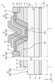
- FIG. 1 is a cross-sectional view of a nitride semiconductor device according to Embodiment 1.
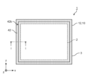
- FIG. FIG. 2 is a plan view of the nitride semiconductor device according to Embodiment 1.
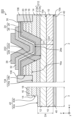
- FIG. 3 is a cross-sectional view of a nitride semiconductor device according to a modification of Embodiment 1.
- FIG. 4 is a cross-sectional view of a nitride semiconductor device according to Embodiment 2.
- FIG. 5 is a cross-sectional view of a nitride semiconductor device according to Modification 1 of Embodiment 2.
- FIG. 6 is a cross-sectional view of a nitride semiconductor device according to Modification 2 of Embodiment 2.
- FIG. 1 is a cross-sectional view of a nitride semiconductor device according to Embodiment 1.
- FIG. 2 is a plan view of the nitride semiconductor device according to Embodiment 1.
- FIG. 3 is a cross-
- a parasitic npn bipolar structure is not formed by an n-type drift layer, a p-type underlayer, and an n-type channel (two-dimensional electron gas).
- a high resistance GaN layer is disposed between the p-type underlayer and the channel. This improves the off characteristics of the transistor.
- channel electrons may be trapped in this high-resistance GaN layer. This is because carbon (C) or iron (Fe) doped in the high-resistance GaN layer generates a trap level. Trapped electrons may degrade the dynamic characteristics of the transistor.
- the present disclosure provides a nitride semiconductor device including a transistor with improved off characteristics while suppressing degradation of dynamic characteristics.
- a nitride semiconductor device includes a substrate, a first semiconductor layer of a first conductivity type disposed above the substrate, and a first semiconductor layer disposed above the first semiconductor layer. a second semiconductor layer having a conductivity type of 2; a third semiconductor layer disposed above the second semiconductor layer and having higher resistance than the second semiconductor layer; and the third semiconductor layer.
- a gate electrode, a source electrode spaced apart from the gate electrode, and a drain electrode located on the lower surface side of the substrate are provided.
- the fourth semiconductor layer is arranged above the high-resistance third semiconductor layer, electrons are less likely to be trapped in the trap level generated in the third semiconductor layer. Therefore, deterioration of the dynamic characteristics of the transistor can be suppressed.
- a high-resistance third semiconductor layer may be arranged at the lowest pn junction (specifically, in contact with the upper surface of the first semiconductor layer).
- the high-resistance third semiconductor layer tends to deteriorate in crystal quality due to doping with carbon or the like. Therefore, if a high-resistance third semiconductor layer is provided in the pn junction portion to which a high electric field is applied when the device is turned off, the off characteristics may deteriorate.
- the second semiconductor layer is arranged below the third semiconductor layer, and the second semiconductor layer and the first semiconductor layer Since a pn junction is formed, off characteristics can be improved.
- the fifth semiconductor layer includes an electron transit layer and an electron supply layer disposed above the electron transit layer, and the distance between the bottom of the electron supply layer and the drain electrode is the It may be shorter than the distance between the bottom of the third semiconductor layer and the drain electrode.
- the electron transit layer and the electron supply layer can be formed continuously by crystal growth. Therefore, the pn junction portion of the interface between the electron transport layer and the electron supply layer (that is, the pn junction portion of the gate portion) has few levels caused by impurities or damage, and has the highest electric field in the nitride semiconductor device. It becomes a part that can withstand strength.
- the pn junction portion of the gate portion close to the drain electrode, the electric field generated between the gate electrode or the source electrode and the drain electrode when turned off can be concentrated to the pn junction portion of the gate portion. This makes it possible to suppress concentration of the electric field on weak portions, thereby improving the OFF characteristics.
- a second opening provided apart from the gate electrode and penetrating the fifth semiconductor layer to reach the fourth semiconductor layer may be provided.
- the source electrode may be provided along the inner surface of the second opening.
- the channel is exposed on the inner surface of the second opening, so that the source electrode can contact the channel at this exposed portion. Therefore, the ohmic contact resistance between the source electrode and the channel can be reduced. Further, since the third semiconductor layer with high resistance is arranged below the fourth semiconductor layer with which the source electrode is in contact at the bottom of the second opening, a parasitic pn diode formed between the source and the drain It is possible to suppress the current from flowing to Thereby, the reliability of the nitride semiconductor device can be improved.
- the nitride semiconductor device is provided apart from the gate electrode, and penetrates through the fifth semiconductor layer, the fourth semiconductor layer, and the third semiconductor layer. and a third opening reaching the second semiconductor layer.
- the source electrode may be provided along the inner surface of the third opening.
- the channel is exposed on the inner surface of the third opening, so that the source electrode can come into contact with the channel at this exposed portion. Therefore, the ohmic contact resistance between the source electrode and the channel can be reduced. Moreover, since the source electrode is in contact with both the fourth semiconductor layer and the second semiconductor layer, the potential of each semiconductor layer can be firmly fixed. This can further improve the off characteristics of the nitride semiconductor device.
- the third semiconductor layer may contain C, Fe, B or Mg.
- the first semiconductor layer may be composed of a plurality of layers having different impurity concentrations, and the impurity concentration of the uppermost layer among the plurality of layers may be the lowest among the plurality of layers.
- the impurity concentration is low in the vicinity of the pn junction portion between the first semiconductor layer and the second semiconductor layer, so that electric field concentration can be alleviated when the semiconductor layer is turned off. Therefore, the off characteristics of the nitride semiconductor device can be improved.
- the bottom of the first opening may be located in the n-th layer from the top (n is a natural number equal to or greater than 2) among the plurality of layers.
- the layer with a low impurity concentration located at the uppermost layer of the first semiconductor layer contributes to the improvement of off characteristics.
- the on-resistance increases.
- the bottom of the first opening penetrates the layer with the low impurity concentration located at the uppermost layer of the first semiconductor layer, thereby removing the layer with the low impurity concentration from the current path during the ON state. can be done. Therefore, on-resistance can be reduced.
- a layer with a low impurity concentration does not contribute to the improvement of off characteristics.
- the pn junction portion of the interface between the electron transit layer and the electron supply layer can receive an electric field, it is possible to suppress the deterioration of the off-characteristics. This is because the pn junction portion of the gate portion is the portion that can withstand the highest electric field strength in the nitride semiconductor device.
- a groove portion reaching the first semiconductor layer may be provided at the end portion of the nitride semiconductor device. Further, for example, the distance between the bottom of the first opening and the drain electrode may be shorter than the distance between the bottom of the trench and the drain electrode.
- the trench at the end of the device is likely to be damaged by etching during formation, and the electric field strength that it can endure may not be sufficient.
- the pn junction portion of the gate portion can receive the electric field at the time of OFF, so that the deterioration of the OFF characteristics can be suppressed.
- each figure is a schematic diagram and is not necessarily strictly illustrated. Therefore, for example, scales and the like do not necessarily match in each drawing. Moreover, in each figure, substantially the same configurations are denoted by the same reference numerals, and overlapping descriptions are omitted or simplified.
- the x-axis, y-axis and z-axis indicate the three axes of a three-dimensional orthogonal coordinate system.
- the x-axis and the y-axis are directions parallel to the first side of the rectangle and the second side orthogonal to the first side, respectively, when the substrate has a rectangular shape in plan view.
- the z-axis is the thickness direction of the substrate.
- the "thickness direction" of the substrate refers to the direction perpendicular to the main surface of the substrate.
- the thickness direction is the same as the stacking direction of the semiconductor layers, and is also referred to as the “longitudinal direction”.
- a direction parallel to the main surface of the substrate may be referred to as a "lateral direction”.
- the side of the substrate on which the gate electrode and the source electrode are provided (the positive side of the z-axis) is regarded as the “upper side” or the “upper side”
- the side of the substrate on which the drain electrode is provided (the negative side of the z-axis) is regarded as the “upper side”. side) as "lower” or "lower”.
- the terms “upper” and “lower” do not refer to the upward direction (vertically upward) and the downward direction (vertically downward) in absolute spatial recognition, but are based on the stacking order in the stacking structure. It is used as a term defined by a relative positional relationship. Also, the terms “above” and “below” are used not only when two components are spaced apart from each other and there is another component between the two components, but also when two components are spaced apart from each other. It also applies when two components are in contact with each other and are placed in close contact with each other.
- planar view means when viewed from a direction perpendicular to the main surface of the substrate of the nitride semiconductor device, that is, when the main surface of the substrate is viewed from the front. .
- ordinal numbers such as “first” and “second” do not mean the number or order of constituent elements unless otherwise specified, so as to avoid confusion between constituent elements of the same kind and to distinguish them from each other. It is used for the purpose of
- AlGaN represents a ternary mixed crystal Al x Ga 1-x N (0 ⁇ x ⁇ 1).
- multi-element mixed crystals are abbreviated by the arrangement of their constituent element symbols, eg, AlInN, GaInN, and the like.
- AlxGa1 -xyInyN ( 0 ⁇ x ⁇ 1, 0 ⁇ y ⁇ 1, and 0 ⁇ x+y ⁇ 1), which is an example of a nitride semiconductor, is abbreviated as AlGaInN.
- FIG. 1 is a cross-sectional view of a nitride semiconductor device 1 according to this embodiment.
- FIG. 2 is a plan view of nitride semiconductor device 1 according to the present embodiment.
- FIG. 1 shows a cross section taken along line II of FIG.
- the transistor portion 2 and the terminal portion 3 are schematically shown separately.
- the nitride semiconductor device 1 includes a transistor portion 2 and a termination portion 3.
- the nitride semiconductor device 1 includes a substrate 10, a drift layer 12, a first underlayer 14, an intermediate high resistance layer 16, a second underlayer 18, and a third underlayer 20. , a gate opening 22 , a semiconductor laminated film 24 , a threshold adjustment layer 32 , a source opening 34 , a source electrode 36 , a gate electrode 38 and a drain electrode 40 .
- the semiconductor laminate film 24 is a laminate of an electron transit layer 26 and an electron supply layer 28, and includes a two-dimensional electron gas (2DEG) 30 as a channel region.
- Nitride semiconductor device 1 also includes groove portion 42 provided in terminal portion 3 .
- the transistor section 2 is a region containing FETs, and is a region containing the center of the nitride semiconductor device 1 as shown in FIG. Specifically, the transistor portion 2 is a region in which the third underlying layer 20, the gate opening portion 22, the semiconductor laminated film 24, the threshold adjustment layer 32, the source electrode 36 or the gate electrode 38 are arranged in plan view. .
- each component arranged in the transistor section 2 is omitted.
- a plurality of source electrodes 36 elongated in one direction in plan view are arranged in stripes, and gate electrodes 38, threshold adjustment layers 32, and gate openings 22 are arranged between adjacent source electrodes 36.
- a plurality of source electrodes 36 having a hexagonal planar shape may be arranged so as to be planarly filled with a gap between them.
- the terminal portion 3 is a region other than the transistor portion 2 and is provided in a ring shape surrounding the transistor portion 2 .
- the third underlying layer 20 , the gate opening 22 , the semiconductor laminated film 24 , the threshold adjustment layer 32 , the source electrode 36 and the gate electrode 38 are not arranged in the terminal portion 3 .
- the nitride semiconductor device 1 is a device having a laminated structure of semiconductor layers mainly composed of nitride semiconductors such as GaN and AlGaN. Specifically, nitride semiconductor device 1 has a heterostructure of an AlGaN film and a GaN film.
- a high-concentration two-dimensional electron gas 30 is generated at the heterointerface by spontaneous polarization or piezoelectric polarization on the (0001) plane. Therefore, even in an undoped state, a sheet carrier concentration of 1 ⁇ 10 13 cm ⁇ 2 or more can be obtained at the interface.
- the nitride semiconductor device 1 is a field effect transistor (FET) that uses a two-dimensional electron gas 30 generated at the AlGaN/GaN heterointerface as a channel.
- FET field effect transistor
- the nitride semiconductor device 1 is a so-called vertical FET.
- the nitride semiconductor device 1 is a normally-off FET.
- the source electrode 36 is grounded (that is, the potential is 0 V), and the drain electrode 40 is given a positive potential.
- the potential applied to the drain electrode 40 is, for example, 100 V or more and 1200 V or less, but is not limited to this.
- gate electrode 38 is applied with 0 V or a negative potential (eg, -5 V).
- gate electrode 38 is applied with a positive potential (for example, +5 V).
- Nitride semiconductor device 1 may be a normally-on FET.
- the substrate 10 is a substrate made of a nitride semiconductor, and has a first principal surface 10a and a second principal surface 10b facing each other, as shown in FIG.
- the first main surface 10a is the main surface (upper surface) on which the drift layer 12 is formed.
- the first main surface 10a substantially coincides with the c-plane.
- the second main surface 10b is the main surface (lower surface) on which the drain electrode 40 is formed.
- the planar view shape of the substrate 10 is, for example, a rectangle, but is not limited to this.
- the substrate 10 is, for example, a substrate made of n + -type GaN having a thickness of 300 ⁇ m and a carrier concentration of 1 ⁇ 10 18 cm ⁇ 3 .
- n-type and p-type indicate conductivity types of semiconductors.
- the n + type represents a state in which an n-type dopant is added to a semiconductor at a high concentration, that is, so-called heavy doping.
- n ⁇ type represents a state in which an n-type dopant is added to a semiconductor at a low concentration, ie, so-called light doping. The same is true for p + -type and p - -type.
- N-type, n + -type and n - -type are examples of the first conductivity type.
- P-type, p + -type and p - -type are examples of the second conductivity type.
- the second conductivity type is a conductivity type opposite in polarity to the first conductivity type.
- the substrate 10 does not have to be a nitride semiconductor substrate.
- the substrate 10 may be a silicon (Si) substrate, a silicon carbide (SiC) substrate, a zinc oxide (ZnO) substrate, or the like.
- the drift layer 12 is an example of a first conductivity type first semiconductor layer disposed above the substrate 10 .
- the drift layer 12 is, for example, a film made of n ⁇ -type GaN with a thickness of 8 ⁇ m.
- the donor concentration of the drift layer 12 is, for example, in the range of 1 ⁇ 10 15 cm ⁇ 3 or more and 1 ⁇ 10 17 cm ⁇ 3 or less, and is 1 ⁇ 10 16 cm ⁇ 3 as an example.
- the carbon concentration (C concentration) of the drift layer 12 is in the range of 1 ⁇ 10 15 cm ⁇ 3 to 2 ⁇ 10 17 cm ⁇ 3 .
- the drift layer 12 is provided in contact with the first main surface 10a of the substrate 10, for example.
- the drift layer 12 is formed on the first main surface 10a of the substrate 10 by, for example, crystal growth such as metal-organic vapor phase epitaxy (MOVPE).
- MOVPE metal-organic vapor phase epitaxy
- the first underlayer 14 is an example of a second conductivity type second semiconductor layer disposed above the drift layer 12 .
- the first underlayer 14 is, for example, a film made of p-type GaN having a thickness of 400 nm and a carrier concentration of 1 ⁇ 10 17 cm ⁇ 3 .
- the first underlayer 14 is provided in contact with the upper surface of the drift layer 12 .
- the first underlayer 14 is formed on the drift layer 12 by, for example, crystal growth such as the MOVPE method.
- the first underlayer 14 may be formed by ion-implanting magnesium (Mg) into a deposited undoped GaN film.
- Mg ion-implanting magnesium
- undoped means that the GaN is not doped with a dopant such as Si or Mg that changes the polarity of GaN to n-type or p-type.
- the intermediate high-resistance layer 16 is an example of a third semiconductor layer arranged above the first underlying layer 14 .
- the intermediate high-resistance layer 16 is a high-resistance layer having a resistance higher than that of the first underlying layer 14 .
- the intermediate high resistance layer 16 is made of an insulating or semi-insulating nitride semiconductor.
- the intermediate high resistance layer 16 is, for example, a GaN film with a thickness of 200 nm.
- the intermediate high resistance layer 16 is provided in contact with the first underlying layer 14 .
- the intermediate high resistance layer 16 contains carbon (C).
- the carbon concentration of the intermediate high resistance layer 16 is higher than the carbon concentration of each of the first underlayer 14 and the second underlayer 18 .
- the carbon concentration of the intermediate high resistance layer 16 is, for example, 3 ⁇ 10 17 cm ⁇ 3 or more, but may be 1 ⁇ 10 18 cm ⁇ 3 or more.
- the intermediate high-resistance layer 16 may contain silicon (Si) or oxygen (O) mixed during film formation.
- the carbon concentration of the intermediate high resistance layer 16 is higher than the silicon concentration (Si concentration) or the oxygen concentration (O concentration).
- the silicon concentration or oxygen concentration of the intermediate high resistance layer 16 is, for example, 5 ⁇ 10 16 cm ⁇ 3 or less, but may be 2 ⁇ 10 16 cm ⁇ 3 or less.
- the intermediate high-resistance layer 16 may contain magnesium (Mg), iron (Fe), boron (B), or the like instead of or in addition to carbon.
- the intermediate high resistance layer 16 may contain other impurities as long as they are impurities capable of increasing the resistance of GaN.
- the intermediate high-resistance layer 16 is formed on the first underlayer 14 by, for example, crystal growth such as the MOVPE method.
- the intermediate high-resistance layer 16 may be formed by ion-implanting an impurity into a deposited undoped GaN film.
- the second underlying layer 18 is an example of a fourth semiconductor layer of the second conductivity type arranged above the intermediate high-resistance layer 16 .
- the second underlayer 18 is, for example, a film made of p-type GaN having a thickness of 200 nm and a carrier concentration of 1 ⁇ 10 17 cm ⁇ 3 .
- the second underlayer 18 is provided in contact with the upper surface of the intermediate high-resistance layer 16 .
- the second underlayer 18 is formed on the intermediate high-resistance layer 16 by, for example, crystal growth such as the MOVPE method.
- the second underlayer 18 may be formed by ion-implanting magnesium (Mg) into the deposited undoped GaN film.
- the third underlayer 20 is an undoped semiconductor layer arranged above the second underlayer 18 .
- the third underlayer 20 is, for example, a film made of undoped AlGaN with a thickness of 150 nm.
- the third underlayer 20 may be a film made of GaN, InAlN or InAlGaN.
- the third underlayer 20 is provided in contact with the upper surface of the second underlayer 18 .
- the third underlayer 20 is formed on the second underlayer 18 by, for example, crystal growth such as the MOVPE method.
- the drift layer 12, the first underlayer 14, the intermediate high-resistance layer 16, the second underlayer 18, and the third underlayer 20 can be continuously formed in the same chamber.
- the gate opening 22 is an example of a first opening penetrating the third underlying layer 20, the second underlying layer 18, the intermediate high resistance layer 16 and the first underlying layer 14 and reaching the drift layer 12. .
- Bottom 22 a of gate opening 22 is part of the upper surface of drift layer 12 .
- the bottom portion 22a is located below the lower surface of the first underlayer 14.
- the lower surface of the first underlayer 14 corresponds to the interface between the first underlayer 14 and the drift layer 12 .
- the bottom portion 22a is parallel to the first major surface 10a of the substrate 10, for example.
- the gate opening 22 is formed such that the opening area increases as the distance from the substrate 10 increases. Specifically, the sidewall 22b of the gate opening 22 is obliquely inclined. As shown in FIG. 1, the cross-sectional shape of the gate opening 22 is an inverted trapezoid, more specifically, an inverted isosceles trapezoid.
- the inclination angle of the side wall 22b with respect to the bottom portion 22a is, for example, in the range of 30° or more and 45° or less.
- the smaller the tilt angle the closer the side wall 22b is to the c-plane, so the film quality of the electron transit layer 26 formed along the side wall 22b by crystal regrowth can be improved.
- the larger the tilt angle the more the gate opening 22 is prevented from becoming too large, and the size reduction of the nitride semiconductor device 1 is realized.
- the gate opening 22 forms the drift layer 12 , the first underlayer 14 , the intermediate high resistance layer 16 , the second underlayer 18 and the third underlayer 20 on the first main surface 10 a of the substrate 10 .
- a third underlayer 20, a second underlayer 18, an intermediate high resistance layer 16 and a first underlayer 14 are formed so as to partially expose the drift layer 12. is formed by removing a portion of each of At this time, by removing the surface layer portion of the drift layer 12 by a predetermined thickness, the bottom portion 22 a of the gate opening portion 22 is formed below the lower surface of the first underlying layer 14 .
- the removal of the third underlayer 20, the second underlayer 18, the intermediate high-resistance layer 16, and the first underlayer 14 is performed by resist coating and patterning, and dry etching. Specifically, after patterning the resist, baking is performed so that the edges of the resist are slanted. By performing dry etching after that, the gate opening 22 is formed so that the side wall 22b is slanted so that the shape of the resist is transferred.
- the semiconductor laminated film 24 is an example of a fifth semiconductor layer partly arranged along the inner surface of the gate opening 22 and partly arranged above the second underlying layer 18 . That is, a part of the semiconductor laminated film 24 is arranged along the inner surface of the gate opening 22 and another part of the semiconductor laminated film 24 is arranged above the second underlying layer 18 .
- the semiconductor laminated film 24 is a laminated film of an electron transit layer 26 and an electron supply layer 28 .
- the electron transit layer 26 is an example of a first regrowth layer provided along the inner surface of the gate opening 22 . Specifically, part of the electron transit layer 26 is provided along the bottom 22 a and sidewalls 22 b of the gate opening 22 , and the other part of the electron transit layer 26 is provided on the upper surface of the third underlying layer 20 . is provided.
- the electron transit layer 26 is, for example, a film made of undoped GaN with a thickness of 150 nm.
- the electron transit layer 26 may be made n-type by Si doping instead of undoping.
- the electron transit layer 26 is in contact with the drift layer 12 at the bottom 22a and sidewalls 22b of the gate opening 22.
- the electron transit layer 26 is in contact with the end face of each of the first underlying layer 14, the intermediate high-resistance layer 16, the second underlying layer 18 and the third underlying layer 20 at the sidewall 22b of the gate opening 22. .
- the electron transit layer 26 is in contact with the upper surface of the third underlying layer 20 .
- the electron transit layer 26 is formed by crystal regrowth after the gate opening 22 is formed.
- the electron transit layer 26 has a first conductivity type channel region. Specifically, a two-dimensional electron gas 30 is generated near the interface between the electron transit layer 26 and the electron supply layer 28 . A two-dimensional electron gas 30 functions as a channel of the electron transit layer 26 . In FIG. 1, the two-dimensional electron gas 30 is schematically illustrated by broken lines. The two-dimensional electron gas 30 bends along the interface between the electron transit layer 26 and the electron supply layer 28 , that is, along the inner surface of the gate opening 22 .
- an AlN film having a thickness of about 1 nm may be provided as a second regrowth layer between the electron transit layer 26 and the electron supply layer 28 .
- the AlN film can suppress alloy scattering and improve channel mobility.
- the electron supply layer 28 is an example of a third regrowth layer provided along the inner surface of the gate opening 22 .
- the electron supply layer 28 is arranged above the electron transit layer 26 .
- the electron supply layer 28 is formed in a shape along the upper surface of the electron transit layer 26 with a substantially uniform thickness.
- the electron supply layer 28 is, for example, a film made of undoped AlGaN with a thickness of 50 nm.
- the electron supply layer 28 is formed by crystal regrowth following the step of forming the electron transit layer 26 .
- the electron supply layer 28 forms an AlGaN/GaN heterointerface with the electron transit layer 26 . As a result, a two-dimensional electron gas 30 is generated within the electron transit layer 26 .
- the electron supply layer 28 supplies electrons to the channel region (that is, the two-dimensional electron gas 30) formed in the electron transit layer 26.
- the threshold adjustment layer 32 is an example of a second conductivity type sixth semiconductor layer disposed above the semiconductor laminated film 24 . Specifically, the threshold adjustment layer 32 is provided between the gate electrode 38 and the electron supply layer 28 . The threshold adjustment layer 32 is formed in a shape along the upper surface of the electron supply layer 28 with a substantially uniform thickness.
- the threshold adjustment layer 32 is, for example, a nitride semiconductor layer made of p-type GaN or AlGaN having a thickness of 100 nm and a carrier concentration of 1 ⁇ 10 17 cm ⁇ 3 .
- the threshold adjustment layer 32 is formed by regrowth by the MOVPE method subsequent to the step of forming the electron supply layer 28 and patterning. Note that the electron transit layer 26, the electron supply layer 28, and the threshold adjustment layer 32 can be continuously formed in this order within the same chamber.
- the threshold adjustment layer 32 raises the potential of the conduction band edge of the channel portion. Therefore, the threshold voltage of nitride semiconductor device 1 can be increased. Therefore, the nitride semiconductor device 1 can be realized as a normally-off FET. That is, when a potential of 0 V is applied to the gate electrode 38, the nitride semiconductor device 1 can be turned off.
- the source opening 34 is an example of a second opening that penetrates the semiconductor laminated film 24 and the third underlying layer 20 and reaches the second underlying layer 18 at a position away from the gate opening 22 .
- the source opening 34 is arranged at a position distant from the gate electrode 38 in plan view.
- a bottom portion 34 a of the source opening 34 is part of the upper surface of the second underlying layer 18 . As shown in FIG. 1, the bottom portion 34a is located below the lower surface of the third underlayer 20. As shown in FIG. The bottom surface of the third underlayer 20 corresponds to the interface between the third underlayer 20 and the second underlayer 18 . The bottom portion 34a is parallel to the first major surface 10a of the substrate 10, for example.
- the source opening 34 is formed so that the opening area is constant regardless of the distance from the substrate 10 .
- sidewalls 34b of source opening 34 are perpendicular to bottom 34a. That is, the cross-sectional shape of the source opening 34 is rectangular.
- the source opening 34 may be formed such that the opening area increases as the distance from the substrate 10 increases, similarly to the gate opening 22 .
- the sidewall 34b of the source opening 34 may be obliquely slanted.
- the cross-sectional shape of the source opening 34 may be an inverted trapezoid, more specifically, an inverted isosceles trapezoid.
- the inclination angle of the side wall 34b with respect to the bottom portion 34a may be, for example, in the range of 30° or more and 60° or less.
- the slope angle of sidewalls 34b of source opening 34 may be greater than the slope angle of sidewalls 22b of gate opening 22 .
- the contact area between the source electrode 36 and the electron transit layer 26 (two-dimensional electron gas 30) is increased, thereby facilitating ohmic connection.
- the two-dimensional electron gas 30 is exposed on the sidewall 34b of the source opening 34 and connected to the source electrode 36 at the exposed portion.
- the source openings 34 are, for example, threshold-adjustable so as to expose the second underlying layer 18 in regions different from the gate openings 22 following the step of forming the threshold-adjusting layer 32 (i.e., the crystal regrowth step). It is formed by etching the adjustment layer 32 , the electron supply layer 28 , the electron transit layer 26 and the third underlying layer 20 . At this time, the surface layer portion of the second underlying layer 18 is also removed, so that the bottom portion 34 a of the source opening 34 is formed below the lower surface of the third underlying layer 20 .
- the source opening 34 is formed into a predetermined shape by, for example, photolithographic patterning and dry etching.
- the source electrode 36 is arranged apart from the gate electrode 38 .
- the source electrode 36 is provided along the inner surface of the source opening 34 .
- the source electrode 36 is connected to each of the electron supply layer 28 , the electron transit layer 26 and the second underlying layer 18 .
- the source electrode 36 is ohmic-connected to each of the electron transit layer 26 and the electron supply layer 28 .
- Source electrode 36 is in direct contact with two-dimensional electron gas 30 at sidewall 34b. Thereby, the contact resistance between the source electrode 36 and the two-dimensional electron gas 30 (channel) can be reduced.
- the source electrode 36 is formed using a conductive material such as metal.
- a material such as Ti/Al that can be ohmic-connected to the n-type GaN layer by heat treatment can be used.
- the source electrode 36 is formed, for example, by patterning a conductive film formed by sputtering or vapor deposition.
- the gate electrode 38 is arranged above the threshold adjustment layer 32 . Specifically, the gate electrode 38 is provided in contact with the upper surface of the threshold adjustment layer 32 so as to cover the gate opening 22 .
- the gate electrode 38 is formed, for example, in a shape along the upper surface of the threshold value adjusting layer 32 with a substantially uniform film thickness. Alternatively, the gate electrode 38 may be formed so as to fill the concave portion of the upper surface of the threshold adjustment layer 32 .
- the gate electrode 38 is formed using a conductive material such as metal.
- the gate electrode 38 is formed using palladium (Pd).
- a material that is Schottky-connected to the p-type GaN layer can be used, such as a nickel (Ni)-based material, tungsten silicide (WSi), gold (Au), or the like.
- the gate electrode 38 is formed by patterning a conductive film formed by, for example, sputtering or vapor deposition after the threshold adjustment layer 32 is formed, the source opening 34 is formed, or the source electrode 36 is formed. be.
- the drain electrode 40 is provided on the lower surface side of the substrate 10 , that is, on the side opposite to the drift layer 12 . Specifically, the drain electrode 40 is provided in contact with the second main surface 10b of the substrate 10 .
- the drain electrode 40 is formed using a conductive material such as metal.
- a material such as Ti/Al that is ohmic-connected to the n-type GaN layer can be used.
- the drain electrode 40 is formed, for example, by patterning a conductive film deposited by sputtering or vapor deposition.
- the third underlying layer 20, the semiconductor laminated film 24 and the threshold adjustment layer 32 are not provided.
- the third underlying layer 20, the semiconductor laminated film 24, and the threshold adjustment layer 32 are removed at the termination portion 3 at the same time as the source opening portion 34 is formed.
- the top surface of the second underlying layer 18 is positioned at the same height as the bottom portion 34 a of the source opening 34 .
- “same height” means that the distances from the first major surface 10a of the substrate 10 are the same.
- a groove portion 42 is provided in the terminal end portion 3 .
- the groove portion 42 is an isolation trench for partitioning and isolating the transistor portion 2 .
- the groove portion 42 penetrates the second underlayer 18 , the intermediate high-resistance layer 16 and the first underlayer 14 and reaches the drift layer 12 .
- the groove portion 42 has a bottom portion 42a and side walls 42b.
- the groove portion 42 is a stepped portion having sidewalls 42b only on the transistor portion 2 side. That is, the bottom portion 42a of the groove portion 42 is connected to the end face of the nitride semiconductor device 1. As shown in FIG.
- the groove portion 42 is provided in a ring shape surrounding the transistor portion 2, as shown in FIG.
- a bottom portion 42 a of the groove portion 42 is part of the upper surface of the drift layer 12 . As shown in FIG. 1, the bottom portion 42a is located below the lower surface of the first underlayer 14. As shown in FIG. The bottom portion 42a is parallel to the first major surface 10a of the substrate 10, for example.
- the groove part 42 is formed so that the opening area is constant regardless of the distance from the substrate 10 .
- sidewalls 42b of groove 42 are perpendicular to bottom 42a. That is, the cross-sectional shape of the groove portion 42 is rectangular.
- the trench 42 is formed, for example, by performing dry etching using a different etching mask following the dry etching process for forming the source opening 34 .
- the trench 42 may be formed by dry etching.
- a p-type first underlayer 14 between the source electrode 36 and the drain electrode 40 , a p-type first underlayer 14 , an intermediate high-resistance layer 16 , and a p-type second and a lamination structure of the underlayer 18 are provided. That is, the intermediate high-resistance layer 16 with high resistance is sandwiched between two p-type semiconductor layers.
- the intermediate high-resistance layer 16 is, as described above, a nitride semiconductor layer such as GaN that is doped with an impurity such as carbon to have a high resistance.
- the doped impurities can generate trap levels in the intermediate high resistance layer 16 .
- the second underlayer 18 is arranged above the intermediate high-resistance layer 16 , electrons in the channel are less likely to be trapped in the trap level of the intermediate high-resistance layer 16 . As a result, deterioration of the dynamic characteristics of the transistor section 2 can be suppressed.
- a first underlayer 14 is arranged below the intermediate high-resistance layer 16 . Leakage current between the source electrode 36 and the drain electrode 40 can be suppressed by providing the first underlying layer 14 .
- the potential of the drain electrode 40 becomes higher than that of the source electrode 36.
- a depletion layer extends in the drift layer 12 . This makes it possible to increase the breakdown voltage of the nitride semiconductor device 1 .
- the potential of the drain electrode 40 is higher than that of the source electrode 36 both in the OFF state and the ON state. Therefore, the nitride semiconductor device 1 can have a high breakdown voltage.
- the intermediate high-resistance layer 16 may be arranged between the first underlayer 14 and the drift layer 12 .
- the intermediate high-resistance layer 16 tends to deteriorate in crystal quality due to being doped with carbon or the like. Therefore, if it is provided at a pn junction where a high electric field is applied during OFF, the OFF characteristics may deteriorate.
- the electron transit layer 26, the p-type first underlayer 14 and the second underlayer 14 would be interposed between the source electrode 36 and the drain electrode 40.
- a parasitic npn structure consisting of the underlying layer 18 and the n-type drift layer 12, that is, a parasitic bipolar transistor exists. Therefore, when the nitride semiconductor device 1 is in the off state, if a current flows through the p-type first base layer 14 or the second base layer 18, the parasitic bipolar transistor is turned on, and the nitride semiconductor device 1 is turned on. There is a possibility that the breakdown voltage of the physical semiconductor device 1 is lowered.
- intermediate high-resistance layer 16 suppresses the formation of a parasitic npn structure, thereby suppressing malfunction of nitride semiconductor device 1 .
- a source opening 34 reaching the second underlying layer 18 is provided. Since the channel (two-dimensional electron gas 30) is exposed on the sidewall 34b of the source opening 34, the source electrode 36 can contact the channel at this exposed portion. Therefore, the ohmic contact resistance between the source electrode 36 and the channel can be reduced.
- the intermediate high-resistance layer 16 is arranged below the second underlying layer 18 with which the source electrode 36 is in contact at the bottom 34a of the source opening 34, a parasitic pn diode formed between the source and the drain is prevented. It is possible to suppress the flow of current. Thereby, the reliability of the nitride semiconductor device 1 can be improved.
- a distance D1 is the distance between the bottom portion 28a of the electron supply layer 28 and the drain electrode 40 .
- a distance D2 is the distance between the bottom portion 16a of the intermediate high-resistance layer 16 and the drain electrode 40.
- the bottom portion 28 a of the electron supply layer 28 is the portion of the lower surface of the electron supply layer 28 closest to the drain electrode 40 . Specifically, it is a portion of the lower surface of the electron supply layer 28 that is positioned within the gate opening 22 and parallel to the bottom 22 a of the gate opening 22 .
- the bottom portion 16 a of the intermediate high-resistance layer 16 is the portion of the lower surface of the intermediate high-resistance layer 16 closest to the drain electrode 40 .
- the lower surface of the intermediate high-resistance layer 16 is parallel to the upper surface of the drain electrode 40 (the second main surface 10b of the substrate 10), so the bottom portion 16a is an arbitrary portion of the lower surface of the intermediate high-resistance layer 16. becomes part of
- the electron transit layer 26 and the electron supply layer 28 can be continuously formed by crystal growth. Therefore, the pn junction portion of the interface between the electron transit layer 26 and the electron supply layer 28, that is, the bottom portion 28a of the electron supply layer 28, has few levels caused by impurities or damage, and the nitride semiconductor device 1 has a It becomes the part that can withstand the highest electric field intensity.
- the electric field generated between the gate electrode 38 or the source electrode 36 and the drain electrode 40 when turned off can be concentrated to the bottom portion 28a of the electron supply layer 28. . This makes it possible to suppress concentration of the electric field on weak portions, thereby improving the OFF characteristics.
- FIG. 3 is a cross-sectional view of nitride semiconductor device 101 according to a modification of the present embodiment.
- nitride semiconductor device 101 has source opening 134 and source electrode 136 instead of source opening 34 and source electrode 36, compared to nitride semiconductor device 1 shown in FIG.
- the difference is that the In the following, the description will focus on the points of difference from the embodiment, and the description of the common points may be omitted or simplified.
- the source opening 134 penetrates the semiconductor laminated film 24 , the third underlying layer 20 , the second underlying layer 18 , and the intermediate high-resistance layer 16 at a position away from the gate opening 22 to form the first underlying layer 14 . It is an example of a third opening reaching to.
- the source opening 134 is arranged at a position distant from the gate electrode 38 in plan view.
- a bottom 134 a of the source opening 134 is part of the upper surface of the first underlying layer 14 . As shown in FIG. 3, the bottom portion 134a is located below the lower surface (bottom portion 16a) of the intermediate high resistance layer 16. As shown in FIG. Note that the lower surface of the intermediate high-resistance layer 16 corresponds to the interface between the intermediate high-resistance layer 16 and the first underlayer 14 .
- the source opening 134 reaches the first underlying layer 14 . Since the source electrode 136 is provided along the inner surface of the source opening 134 , it is in contact with the first underlying layer 14 . Specifically, the source electrode 136 is connected to each of the electron supply layer 28 , the electron transit layer 26 , the second underlying layer 18 and the first underlying layer 14 .
- the channel (two-dimensional electron gas 30) is exposed on the side wall 34b of the source opening 134, so that the source electrode 136 can contact the channel at this exposed portion. Therefore, the ohmic contact resistance between the source electrode 136 and the channel can be reduced.
- the source electrode 136 is in contact with both the second underlying layer 18 and the first underlying layer 14, the potential of each layer can be firmly fixed. Thereby, the off characteristics of the nitride semiconductor device 1 can be further improved.
- the second base layer 18 and the intermediate high-resistance layer 16 may be provided in the terminal portion 3 . That is, in the terminal portion 3 , the second underlying layer 18 and the intermediate high-resistance layer 16 may be removed simultaneously with the formation of the source opening 134 to expose the upper surface of the first underlying layer 14 .
- the nitride semiconductor device according to Embodiment 2 differs from Embodiment 1 in that the drift layer includes a plurality of layers with different impurity concentrations.
- the description will focus on the differences from the first embodiment and its modification, and the description of the common points may be omitted or simplified.
- FIG. 4 is a cross-sectional view of nitride semiconductor device 201 according to the present embodiment.
- nitride semiconductor device 201 differs from nitride semiconductor device 1 according to Embodiment 1 in that drift layer 212 is provided instead of drift layer 12 .
- the drift layer 212 is composed of a plurality of layers with different impurity concentrations.
- the plurality of layers is composed of two layers.
- the drift layer 212 has a high concentration layer 212a and a low concentration layer 212b.
- the high-concentration layer 212a and the low-concentration layer 212b are formed continuously on the substrate 10 by, for example, crystal growth such as the MOVPE method.
- the high-concentration layer 212a is an example of the n-th layer from the top among the plurality of layers. n is a natural number of 2 or more. In this embodiment, n is two. The high-concentration layer 212a is provided in contact with the first major surface 10a of the substrate 10 .
- the high-concentration layer 212a is, for example, a film made of n + -type GaN with a thickness of 7 ⁇ m.
- the impurity concentration (donor concentration) of the high-concentration layer 212a is, for example, in the range of 3 ⁇ 10 15 cm ⁇ 3 or more and 5 ⁇ 10 16 cm ⁇ 3 or less, and is 1.5 ⁇ 10 16 cm ⁇ 3 as an example. .
- the low-concentration layer 212b is an example of a layer located above the n-th layer.
- the low-concentration layer 212b is the uppermost layer in the drift layer 212, and is provided between the high-concentration layer 212a and the first underlayer 14 in contact with each other.
- the impurity concentration of the low-concentration layer 212 b is the lowest among the plurality of layers forming the drift layer 212 . That is, the impurity concentration of the low concentration layer 212b is lower than the impurity concentration of the high concentration layer 212a.
- the low-concentration layer 212b is, for example, a film made of n ⁇ -type GaN with a thickness of 1 ⁇ m.
- the impurity concentration (donor concentration) of the low-concentration layer 212b is, for example, in the range of 1 ⁇ 10 15 cm ⁇ 3 or more and 3 ⁇ 10 16 cm ⁇ 3 or less, and is 9 ⁇ 10 15 cm ⁇ 3 as an example.
- the OFF state is achieved.
- a high voltage is applied to the drain electrode 40 in , extension of the depletion layer into the drift layer 212 is promoted. Thereby, the withstand voltage of the nitride semiconductor device 201 can be increased.
- FIG. 5 is a cross-sectional view of a nitride semiconductor device 202 according to this modification.
- nitride semiconductor device 202 has source opening 134 and source electrode 136 instead of source opening 34 and source electrode 36, compared to nitride semiconductor device 201 shown in FIG. The difference is that the Source opening 134 and source electrode 136 are the same as source opening 134 and source electrode 136 according to the modification of the first embodiment.
- the effects of both the nitride semiconductor devices 101 and 201 can be obtained. Specifically, according to the nitride semiconductor device 202, the OFF characteristics can be further improved, and the breakdown voltage can be increased.
- FIG. 6 is a cross-sectional view of a nitride semiconductor device 203 according to this modification.
- the nitride semiconductor device 203 differs from the nitride semiconductor device 202 shown in FIG. 5 in that it has a gate opening 222 instead of the gate opening 22.
- the gate opening 222 penetrates the third underlying layer 20, the second underlying layer 18, the intermediate high resistance layer 16, the first underlying layer 14, and the low concentration layer 212b to reach the high concentration layer 212a.
- the bottom 222a of the gate opening 222 is part of the upper surface of the high concentration layer 212a. As shown in FIG. 1, the bottom portion 222a is located below the lower surface of the low concentration layer 212b.
- the lower surface of the low-concentration layer 212b corresponds to the interface between the low-concentration layer 212b and the high-concentration layer 212a.
- the drain current in the ON state flows from the drain electrode 40 through the substrate 10, the high-concentration layer 212a and the two-dimensional electron gas 30 to the source electrode 36. Since the low-concentration layer 212b with high resistance does not exist on the path of the drain current, the on-resistance can be reduced.
- the distance D3 shown in FIG. 6 is shorter than the distance D4.
- a distance D3 is the distance between the bottom portion 222a of the gate opening 222 and the drain electrode 40 .
- a distance D4 is the distance between the bottom portion 42a of the groove portion 42 and the drain electrode 40 .
- the transistor section 2 When the transistor section 2 is in the off state, a high voltage is applied between the drain electrode 40 and the source electrode 136 such that the potential on the drain electrode 40 side is higher than that on the source electrode 136 side. Therefore, in the off state, a high electric field is generated in the vertical direction of the nitride semiconductor device 203 .
- the electric field is more likely to concentrate on the gate opening 222 of the transistor section 2 than on the terminal section 3.
- a concentrated electric field can be received by the pn junction between the electron supply layer 28 and the electron transit layer 26 .
- This pn junction has higher quality and higher electric field strength than the pn junction between the first underlying layer 14 and the drift layer 212 in the vicinity of the groove 42 where etching damage occurs. Since the pn junction having a high electric field intensity can receive the electric field concentration, the electric field concentration on the pn junction near the groove 42 can be alleviated.
- the off characteristics of the nitride semiconductor device 203 can be improved. Specifically, the leak current in the vicinity of the groove portion 42 can be reduced, and the decrease in breakdown voltage can be suppressed. As the difference between the distance D3 and the distance D4 increases, the electric field concentration in the vicinity of the groove 42 can be alleviated.
- the distance D1 may be shorter than the distance D4. As a result, electric field concentration in the vicinity of the groove portion 42 can be alleviated.
- the number of layers may be three or more.
- the bottom portion 222a of the gate opening 222 is located in a layer other than the top layer having the lowest impurity concentration. That is, the bottom portion 222a is located in the n-th layer from the top (n is a natural number equal to or greater than 2) among the plurality of layers forming the drift layer 212 .
- source opening 34 or 134 may not be provided.
- the source electrode 36 or 136 is provided on the upper surface of the semiconductor laminated film 24 at a position away from the threshold adjustment layer 32 .
- the drift layer 12 may have a graded structure in which the impurity concentration (donor concentration) is gradually reduced from the substrate 10 side to the first underlayer 14 side.
- the donor concentration may be controlled by Si as a donor, or by carbon as an acceptor that compensates for Si.
- the termination portion 3 may not include the end surface of the nitride semiconductor device.
- the termination portion 3 is a portion for separating the transistor portion 2 from other devices.
- Another element may be arranged in a region adjacent to the terminal portion 3 of the transistor portion 2 .
- another element is a pn diode utilizing a pn junction between the drift layer 12 and the first underlying layer 14 .
- the nitride semiconductor device comprises a transistor portion 2, a termination portion 3 and a pn diode.
- the first conductivity type may be p-type, p+ type, or p ⁇ type
- the second conductivity type may be n type, n+ type, or n ⁇ type.
- the present disclosure can be used as a nitride semiconductor device with improved electrical characteristics, and can be used, for example, in power devices such as power transistors used in power circuits of consumer equipment such as televisions.
Landscapes
- Junction Field-Effect Transistors (AREA)
Priority Applications (2)
| Application Number | Priority Date | Filing Date | Title |
|---|---|---|---|
| JP2023567528A JPWO2023112374A1 (https=) | 2021-12-16 | 2022-07-28 | |
| US18/671,465 US20240313061A1 (en) | 2021-12-16 | 2024-05-22 | Nitride semiconductor device |
Applications Claiming Priority (2)
| Application Number | Priority Date | Filing Date | Title |
|---|---|---|---|
| JP2021-204400 | 2021-12-16 | ||
| JP2021204400 | 2021-12-16 |
Related Child Applications (1)
| Application Number | Title | Priority Date | Filing Date |
|---|---|---|---|
| US18/671,465 Continuation US20240313061A1 (en) | 2021-12-16 | 2024-05-22 | Nitride semiconductor device |
Publications (1)
| Publication Number | Publication Date |
|---|---|
| WO2023112374A1 true WO2023112374A1 (ja) | 2023-06-22 |
Family
ID=86774202
Family Applications (1)
| Application Number | Title | Priority Date | Filing Date |
|---|---|---|---|
| PCT/JP2022/029063 Ceased WO2023112374A1 (ja) | 2021-12-16 | 2022-07-28 | 窒化物半導体デバイス |
Country Status (3)
| Country | Link |
|---|---|
| US (1) | US20240313061A1 (https=) |
| JP (1) | JPWO2023112374A1 (https=) |
| WO (1) | WO2023112374A1 (https=) |
Families Citing this family (1)
| Publication number | Priority date | Publication date | Assignee | Title |
|---|---|---|---|---|
| KR20240114185A (ko) * | 2023-01-16 | 2024-07-23 | 삼성전자주식회사 | 반도체 소자 및 그 제조방법 |
Citations (5)
| Publication number | Priority date | Publication date | Assignee | Title |
|---|---|---|---|---|
| WO2012046480A1 (ja) * | 2010-10-06 | 2012-04-12 | 住友電気工業株式会社 | 半導体装置およびその製造方法 |
| WO2015004853A1 (ja) * | 2013-07-12 | 2015-01-15 | パナソニックIpマネジメント株式会社 | 半導体装置 |
| WO2019187789A1 (ja) * | 2018-03-27 | 2019-10-03 | パナソニック株式会社 | 窒化物半導体装置 |
| WO2020017437A1 (ja) * | 2018-07-17 | 2020-01-23 | パナソニック株式会社 | 窒化物半導体装置 |
| WO2021070469A1 (ja) * | 2019-10-09 | 2021-04-15 | パナソニック株式会社 | 窒化物半導体デバイス |
-
2022
- 2022-07-28 WO PCT/JP2022/029063 patent/WO2023112374A1/ja not_active Ceased
- 2022-07-28 JP JP2023567528A patent/JPWO2023112374A1/ja active Pending
-
2024
- 2024-05-22 US US18/671,465 patent/US20240313061A1/en active Pending
Patent Citations (5)
| Publication number | Priority date | Publication date | Assignee | Title |
|---|---|---|---|---|
| WO2012046480A1 (ja) * | 2010-10-06 | 2012-04-12 | 住友電気工業株式会社 | 半導体装置およびその製造方法 |
| WO2015004853A1 (ja) * | 2013-07-12 | 2015-01-15 | パナソニックIpマネジメント株式会社 | 半導体装置 |
| WO2019187789A1 (ja) * | 2018-03-27 | 2019-10-03 | パナソニック株式会社 | 窒化物半導体装置 |
| WO2020017437A1 (ja) * | 2018-07-17 | 2020-01-23 | パナソニック株式会社 | 窒化物半導体装置 |
| WO2021070469A1 (ja) * | 2019-10-09 | 2021-04-15 | パナソニック株式会社 | 窒化物半導体デバイス |
Also Published As
| Publication number | Publication date |
|---|---|
| US20240313061A1 (en) | 2024-09-19 |
| JPWO2023112374A1 (https=) | 2023-06-22 |
Similar Documents
| Publication | Publication Date | Title |
|---|---|---|
| US10629681B2 (en) | III-nitride devices including a graded depleting layer | |
| JP5469098B2 (ja) | 電界効果トランジスタ及びその製造方法 | |
| CN111902920B (zh) | 氮化物半导体装置 | |
| JP7303807B2 (ja) | 窒化物半導体装置 | |
| US9680001B2 (en) | Nitride semiconductor device | |
| JP7813766B2 (ja) | 窒化物半導体デバイス | |
| WO2017138505A1 (ja) | 半導体装置 | |
| JP7157138B2 (ja) | 窒化物半導体装置 | |
| JP7361723B2 (ja) | 窒化物半導体装置 | |
| US12356650B2 (en) | Semiconductor device and method for manufacturing the same | |
| US12543340B2 (en) | Semiconductor device and method for manufacturing the same | |
| US20250275170A1 (en) | Nitride semiconductor device | |
| JP2025065365A (ja) | 窒化物半導体デバイス | |
| JP2018041933A (ja) | 半導体装置及び半導体基板 | |
| WO2021079686A1 (ja) | 窒化物半導体装置 | |
| WO2023042617A1 (ja) | 半導体装置 | |
| US20240313061A1 (en) | Nitride semiconductor device | |
| JP6639260B2 (ja) | 半導体装置 | |
| US12527023B2 (en) | Nitride semiconductor device | |
| JP2016134563A (ja) | 半導体装置 | |
| US20240332372A1 (en) | Nitride semiconductor device | |
| US20240332413A1 (en) | Hemt device having an improved gate structure and manufacturing process thereof | |
| JP2023133798A (ja) | 窒化物半導体デバイス | |
| JP2025125348A (ja) | 窒化物半導体デバイス | |
| WO2026048168A1 (ja) | 窒化物半導体デバイス |
Legal Events
| Date | Code | Title | Description |
|---|---|---|---|
| 121 | Ep: the epo has been informed by wipo that ep was designated in this application |
Ref document number: 22906911 Country of ref document: EP Kind code of ref document: A1 |
|
| WWE | Wipo information: entry into national phase |
Ref document number: 2023567528 Country of ref document: JP |
|
| NENP | Non-entry into the national phase |
Ref country code: DE |
|
| 122 | Ep: pct application non-entry in european phase |
Ref document number: 22906911 Country of ref document: EP Kind code of ref document: A1 |