WO2023106018A1 - ウェハ製造方法 - Google Patents
ウェハ製造方法 Download PDFInfo
- Publication number
- WO2023106018A1 WO2023106018A1 PCT/JP2022/041571 JP2022041571W WO2023106018A1 WO 2023106018 A1 WO2023106018 A1 WO 2023106018A1 JP 2022041571 W JP2022041571 W JP 2022041571W WO 2023106018 A1 WO2023106018 A1 WO 2023106018A1
- Authority
- WO
- WIPO (PCT)
- Prior art keywords
- ingot
- wafer
- laser beam
- irradiation
- absorption coefficient
- Prior art date
Links
Images


Classifications
-
- B—PERFORMING OPERATIONS; TRANSPORTING
- B23—MACHINE TOOLS; METAL-WORKING NOT OTHERWISE PROVIDED FOR
- B23K—SOLDERING OR UNSOLDERING; WELDING; CLADDING OR PLATING BY SOLDERING OR WELDING; CUTTING BY APPLYING HEAT LOCALLY, e.g. FLAME CUTTING; WORKING BY LASER BEAM
- B23K26/00—Working by laser beam, e.g. welding, cutting or boring
- B23K26/50—Working by transmitting the laser beam through or within the workpiece
- B23K26/53—Working by transmitting the laser beam through or within the workpiece for modifying or reforming the material inside the workpiece, e.g. for producing break initiation cracks
-
- H—ELECTRICITY
- H01—ELECTRIC ELEMENTS
- H01L—SEMICONDUCTOR DEVICES NOT COVERED BY CLASS H10
- H01L21/00—Processes or apparatus adapted for the manufacture or treatment of semiconductor or solid state devices or of parts thereof
- H01L21/02—Manufacture or treatment of semiconductor devices or of parts thereof
- H01L21/04—Manufacture or treatment of semiconductor devices or of parts thereof the devices having at least one potential-jump barrier or surface barrier, e.g. PN junction, depletion layer or carrier concentration layer
- H01L21/18—Manufacture or treatment of semiconductor devices or of parts thereof the devices having at least one potential-jump barrier or surface barrier, e.g. PN junction, depletion layer or carrier concentration layer the devices having semiconductor bodies comprising elements of Group IV of the Periodic System or AIIIBV compounds with or without impurities, e.g. doping materials
- H01L21/30—Treatment of semiconductor bodies using processes or apparatus not provided for in groups H01L21/20 - H01L21/26
- H01L21/302—Treatment of semiconductor bodies using processes or apparatus not provided for in groups H01L21/20 - H01L21/26 to change their surface-physical characteristics or shape, e.g. etching, polishing, cutting
- H01L21/304—Mechanical treatment, e.g. grinding, polishing, cutting
Definitions
- the present disclosure relates to a wafer manufacturing method.
- a laser beam having a wavelength that is transparent to SiC is focused inside a SiC single crystal ingot to form a modified layer and cracks extending from this modified layer. It is known to form and cleave.
- the focal point of the laser beam is positioned at a predetermined depth position of the SiC single crystal ingot, and the laser beam is scanned along the cleaved surface to form a modified layer along the cleaved surface.
- the facet region and the non-facet region have different transmittances. Therefore, when trying to form a modified layer by irradiating a laser beam having a wavelength that is transmissive to SiC from the surface of a SiC single crystal ingot to a predetermined depth, the facet region and the non-facet region are: The depth at which the energy density exceeds the threshold at which the modified layer is formed is different.
- the laser beam absorption is different between the facet region and the non-facet region, specifically, that the non-facet region has a lower laser beam absorption than the facet region.
- the intensity of the laser beam reaching the focal point is higher in non-facet areas than in facet areas.
- Patent Document 1 discloses a technique of increasing the energy of the laser beam and raising the position of the collector when irradiating the facet region with the laser beam in the processing and feeding process.
- the "processing and feeding process” is the following process. A focal point of a laser beam of a wavelength transparent to SiC is positioned at a depth corresponding to the thickness of the wafer to be produced from the top surface of the SiC ingot.
- the SiC ingot and the condensing point While irradiating the SiC ingot with a laser beam from the condenser of the laser processing device, the SiC ingot and the condensing point are relatively processed and fed in the X-axis direction, and the SiC is separated into Si and C and on the c-plane. A strip-shaped release layer along which cracks extend is formed.
- there is a certain response delay in raising the condenser and it is not possible to follow the laser beam when it is scanned at high speed.
- moving the light collector up and down causes vibration, which causes variation in the depth of the modified layer, resulting in an increase in material loss.
- the present disclosure has been made in view of the circumstances and the like exemplified above. That is, the present disclosure provides, for example, a wafer manufacturing method capable of increasing manufacturing efficiency more than conventionally by forming a peeling layer satisfactorily over the entire region including the facet region and the non-facet region. .
- a wafer manufacturing method is a method of obtaining wafers from an ingot, comprising: Delamination layer formation of forming a delamination layer at a depth corresponding to the thickness of the wafer from the surface by irradiating a surface on one end side of the ingot in the height direction with a laser beam having transparency; wafer peeling, wherein the wafer precursor, which is a portion between the surface and the peeling layer, is peeled from the ingot at the peeling layer; wafer flattening for flattening the main surface of the plate-shaped peeled body obtained by the wafer peeling; including In forming the release layer, the surface is irradiated with the laser beam so that the facet region is irradiated with a higher frequency than the non-facet region.
- this wafer manufacturing method first, by irradiating the surface of the ingot on the one end side in the height direction with the laser beam having transparency, a depth corresponding to the thickness of the wafer from the surface is irradiated. Then, the release layer is formed. Next, the wafer precursor, which is the portion between the surface of the ingot and the release layer, is released from the ingot at the release layer. Subsequently, the wafer is obtained by flattening the main surface of the plate-shaped peeled body obtained by peeling the wafer precursor from the ingot.
- the intensity of the laser beam reaching the focal point is higher in the non-facet area than in the facet area. Therefore, when forming the peeling layer, the surface is irradiated with the laser beam so that the facet region is irradiated with a higher frequency than the non-facet region.
- the repetition frequency of the laser beam is made higher than in the non-facet region, and the irradiation interval in the first direction is narrowed.
- the irradiation interval of the laser beam in the second direction is narrower than in the non-facet region.
- the facet region is irradiated with the laser beam separately from the irradiation of the laser beam on the entire region including the facet region and the non-facet region.
- this wafer manufacturing method it is possible to satisfactorily form the release layer on the entire region including the facet region and the non-facet region. Therefore, according to such a wafer manufacturing method, it is possible to improve the manufacturing efficiency more than conventionally.
- each element may be given a reference sign with parentheses.
- the reference numerals indicate only one example of the corresponding relationship between the same element and the specific configuration described in the embodiment described later. Therefore, the present disclosure is not limited in any way by the description of the reference numerals.
- FIG. 1 is a side view showing schematic configurations of a wafer, an ingot, and a separation body in a wafer manufacturing method according to an embodiment of the present disclosure
- FIG. 1A to 1D are process diagrams showing an outline of a wafer manufacturing method according to an embodiment of the present disclosure
- FIG. 3 is a side view showing a schematic configuration of an ingot that has undergone a peeling layer forming step shown in FIG. 2
- 3B is a plan view of the ingot shown in FIG. 3A
- FIG. FIG. 3 is a side view schematically showing a release layer forming step shown in FIG. 2 and a release layer forming apparatus used therein
- FIG. 3 is a front view showing the outline of the peeling layer forming step shown in FIG.
- FIGS. 4A and 4B are diagrams schematically showing a release layer forming step shown in FIGS. 4A and 4B;
- FIG. 4A and 4B are diagrams schematically showing a release layer forming step shown in FIGS. 4A and 4B;
- FIG. 4C is a plan view schematically showing a release layer forming step shown in FIGS. 4A and 4B;
- FIG. 4B is an enlarged view of the laser beams shown in FIGS. 4A and 4B near a focal point;
- FIG. 4B is a side view schematically showing the release layer forming step shown in FIG. 4A; It is a side view which shows the outline of the peeling layer formation process in another example.
- FIG. 4C is a plan view schematically showing a release layer forming step shown in FIGS. 4A and 4B;
- FIG. 4B is an enlarged view of the laser beams shown in FIGS. 4A and 4B near a focal point;
- FIG. 4B is a side view schematically
- FIG. 4B is a side view schematically showing the release layer forming step shown in FIG. 4A;
- FIG. 4B is a side view schematically showing the release layer forming step shown in FIG. 4A;
- FIG. 3 is a side view schematically showing the wafer peeling process shown in FIG. 2 and a peeling apparatus used therein;
- FIG. 5B is a plan view showing a modified example of the arrangement of a plurality of laser beams shown in FIG. 5A;
- FIG. 5B is a plan view showing another modified example of the arrangement of a plurality of laser beams shown in FIG. 5A; It is process drawing which shows the outline of the wafer manufacturing method which concerns on a modification.
- FIG. 5B is a plan view schematically showing the release layer forming step shown in FIG. 4A;
- FIG. 4B is a side view schematically showing the release layer forming step shown in FIG. 4A;
- FIG. 3 is a side view schematically showing the wafer peeling process shown in FIG. 2
- FIG. 15 is a plan view showing an example of a mode of setting measurement positions in the wafer optical measurement shown in FIG. 14;
- FIG. 15 is a side cross-sectional view showing a difference in transmittance at a modified layer generation position in the laser slicing, that is, the peeling layer forming step shown in FIG. 14;
- FIG. 15 is a side cross-sectional view showing a difference in transmittance at a modified layer generation position in the laser slicing, that is, the peeling layer forming step shown in FIG.
- FIG. 15 is a side cross-sectional view showing a difference in transmittance at a modified layer generation position in the laser slicing, that is, the peeling layer forming step shown in FIG. 14;
- FIG. 15 is a side cross-sectional view for explaining an example of a method of setting laser beam irradiation conditions in the laser slicing, that is, the peeling layer forming step shown in FIG. 14;
- FIG. 10 is a plan view for explaining a method of deriving an absorption coefficient change amount shown in Equation (2);
- 21 is a graph showing how the absorption coefficient changes in the depth direction of the ingot at the in-plane center position shown in FIG.
- FIG. 15 is a side view showing a first generated body and a second generated body for setting laser beam irradiation conditions in the laser slicing, that is, the peeling layer forming step shown in FIG. 14;
- FIG. 15 is a graph showing how the absorption coefficient changes when the measurement pitch is reduced in some regions in the wafer optical measurement shown in FIG. 14;
- a wafer 1 manufactured by the wafer manufacturing method according to the present embodiment is obtained by slicing an ingot 2 having a substantially cylindrical shape in side view, and having a substantially circular shape in plan view. It is formed in a thin plate shape. That is, the wafer 1 and the ingot 2 have substantially cylindrical side surfaces or end surfaces surrounding the central axis L. As shown in FIG. A central axis L is an imaginary straight line that is parallel to the substantially cylindrical side or end face of the wafer 1 or ingot 2 and passes through the axial center of the wafer 1 or ingot 2 . From the viewpoint of simplification of illustration and explanation, the illustration and explanation of the so-called orientation flat which is usually provided on the wafer 1 and the ingot 2 are omitted in this specification.
- the ingot 2 is a single-crystal SiC ingot having a c-axis Lc and a (0001) plane Pc perpendicular to each other, and has an off angle ⁇ exceeding 0 degrees.
- the c-axis Lc is the crystallographic axis indicated as [0001] by the orientation index.
- the (0001) plane Pc is a crystal plane that is perpendicular to the c-axis Lc and is called a “C plane” in a strict crystallographic sense.
- the off angle ⁇ is an angle between the central axis L of the wafer 1 or ingot 2 and the c-axis Lc, and is, for example, about 1 to 4 degrees.
- the c-axis Lc of the wafer 1 and the ingot 2 is provided in a state in which the central axis L is inclined in the off-angle direction D ⁇ by an off-angle ⁇ exceeding 0 degrees.
- the off-angle direction D ⁇ is the laser-irradiated surface of the wafer 1 or ingot 2 (that is, the upper surface or It is a direction obtained by mapping the movement direction of a point on the center axis L located on the top surface side to the laser irradiation surface.
- right-handed XYZ coordinates are set as shown in FIG.
- the off-angle direction D ⁇ and the X-axis positive direction are assumed to be the same direction.
- the X-axis and the Y-axis are assumed to be parallel to the main surfaces of the wafer 1 and the ingot 2 .
- a "principal surface” is a surface of a plate-like object perpendicular to the plate thickness direction, and may also be referred to as a "top surface", a "bottom surface", or a "plate surface”.
- the “principal surface” is a surface perpendicular to the height direction of a columnar object such as the ingot 2, and can also be called a “top surface” or a “bottom surface”. Furthermore, it is assumed that the thickness direction of the wafer 1 and the height direction of the ingot 2 are parallel to the Z-axis. An arbitrary direction orthogonal to the Z-axis may be hereinafter referred to as an “in-plane direction”.
- the wafer 1 has a wafer C surface 11 and a wafer Si surface 12 which are a pair of main surfaces.
- the wafer 1 is formed such that the wafer C surface 11, which is the upper surface, is inclined at an off angle ⁇ with respect to the (0001) plane Pc.
- the ingot 2 has an ingot C surface 21 and an ingot Si surface 22, which are a pair of main surfaces.
- the ingot 2 is formed such that the ingot C surface 21, which is the top surface, is inclined at an off angle ⁇ with respect to the (0001) plane Pc.
- one end of the ingot 2 in the off-angle direction D ⁇ that is, the upstream end is referred to as a first end 23
- the other end, that is, the downstream end is referred to as a second end 24 .
- the direction in which the wafer C-side 11 and the ingot C-side 21 face is shown as the Z-axis positive direction.
- the ingot 2 has a facet region RF.
- Facet region RF may also be referred to as a "facet portion”.
- a portion of the ingot 2 other than the facet region RF is hereinafter referred to as a non-facet region RN.
- the non-facet region RN may also be referred to as a "non-facet portion”.
- the wafer manufacturing method according to this embodiment is a method for obtaining wafers 1 from ingots 2, and includes the following steps.
- peeling layer forming step A laser beam having a predetermined degree of transparency to the ingot 2 is irradiated to the ingot C surface 21, which is the main surface on one end side in the height direction of the ingot 2.
- a release layer 25 is formed at a depth corresponding to the thickness of the wafer 1 from the surface 21 .
- the “predetermined level of transparency” is a level of transparency that enables formation of a focal point of the laser beam at a depth corresponding to the thickness of the wafer 1 inside the ingot 2 .
- the "depth corresponding to the thickness of the wafer 1" is the thickness of the finished wafer 1 (that is, the target value of the thickness) plus the thickness corresponding to the predetermined processing allowance in the wafer flattening process, etc., which will be described later. , and may also be referred to as "a depth corresponding to the thickness of the wafer 1".
- Wafer peeling process The wafer precursor 26 between the ingot C surface 21 , which is the laser irradiation surface, and the peeling layer 25 is peeled from the ingot 2 at the peeling layer 25 .
- the plate-like object obtained by peeling the wafer precursor 26 from the ingot 2 may be called a "wafer” in socially accepted terms.
- a plate-like object is hereinafter referred to as a "separate body 30".
- the peeling body 30 has a non-peeling surface 31 and a peeling surface 32, which are a pair of main surfaces.
- the non-peeling surface 31 is a surface on which the peeling layer 25 was not formed before the wafer peeling process, and corresponds to the ingot C surface 21 before the peeling layer forming process and the wafer peeling process.
- the peeling surface 32 constitutes the peeling layer 25 before the wafer peeling process, and is a surface newly generated by the wafer peeling process.
- the peeling surface 32 has rough (that is, grinding or polishing required) irregularities resulting from the peeling of the peeling layer 25 and the wafer peeling process.
- Wafer flattening step At least the peeled surface 32 of the non-peeled surface 31 and the peeled surface 32, which are the main surfaces of the peeled body 30, is flattened to obtain the final wafer 1 after manufacturing.
- ECMG and ECMP can be used in addition to general grindstone polishing and CMP.
- CMP is an abbreviation for Chemical Mechanical Polishing.
- ECMG is an abbreviation for Electro-Chemical Mechanical Grinding.
- ECMP is an abbreviation for Electro-Chemical Mechanical Polishing.
- the wafer flattening process can be performed by using these plural types of flattening processes singly or by appropriately combining them.
- Ingot planarization step After detaching the wafer precursor 26, the newly formed upper surface of the ingot 2 is planarized or mirrored so that it can be subjected to the delamination layer forming step again. Also in the ingot flattening process, ECMG and ECMP can be used in addition to general grindstone polishing and CMP. The ingot flattening process can also be performed by using these plural types of flattening processes singly or by appropriately combining them.
- FIG. 2 is a process chart showing a typical example embodying the wafer manufacturing method according to the present embodiment.
- the separated body 30 separated from the ingot 2 through the separation layer forming process and the wafer separation process is finished as an epi-ready wafer 1 through the following processes. ⁇ Rough grinding of the peeled surface 32 to be the wafer Si surface 12 ⁇ ECMG grinding of the peeled surface 32 after rough grinding ⁇ ECMP polishing and cleaning of the peeled surface 32 after ECMG grinding
- the ingot 2 remaining after the separation body 30 is separated from the ingot 2 through the separation layer forming process and the wafer separation process can be subjected to another separation layer forming process through the following processes. ⁇ Rough grinding of the ingot C-side 21 newly generated by the wafer peeling process/finish grinding/cleaning of the ingot C-side 21 after rough grinding
- (Peeling layer forming step) 3A and 3B show the schematic configuration of the ingot 2 in which the release layer 25 and the wafer precursor 26 are formed by the release layer forming step.
- 4A and 4B show an outline of the peeling layer forming process and a schematic configuration of the peeling layer forming apparatus 40 used in this process. It is assumed that the right-handed XYZ coordinates shown in FIGS. 3A to 4B are displayed so as to match the right-handed XYZ coordinates shown in FIG.
- the separation layer 25 is formed by forming a plurality of scanning lines Ls, which are linear laser beam irradiation traces along the X-axis, in the Y-axis direction.
- the scanning line Ls is a line-shaped irradiation mark RM of the laser beam on the ingot 2 .
- the scanning line Ls is provided along the off-angle direction D ⁇ .
- a plurality of scanning lines Ls are arranged in the line feed direction Df.
- the line feed direction Df is an in-plane direction orthogonal to the off-angle direction D ⁇ . That is, the line feed direction Df is a direction perpendicular to the off-angle direction D ⁇ and the height direction of the ingot 2 .
- the release layer forming device 40 includes a chuck table 41 and a light collecting device 42.
- the chuck table 41 is configured to hold the ingot 2 on the ingot Si surface 22 side, which is the bottom surface thereof.
- the chuck table 41 has a suction mechanism or the like that suctions the ingot Si surface 22 by air pressure or the like.
- the method of fixing the ingot 2 to the chuck table 41 is not limited to this aspect.
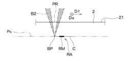
- the light condensing device 42 irradiates the laser beam B oscillated by a pulsed laser oscillator (not shown) to the ingot 2 that is the workpiece fixed to the chuck table 41 , so that the beam axis, which is the irradiation direction of the laser beam B, is radiated. It is arranged facing the chuck table 41 in the direction. That is, the light collecting device 42 is provided so as to irradiate the ingot 2 with the laser beam B from the ingot C surface 21 side, which is the upper surface of the ingot 2 .
- the focusing device 42 is configured to form a focusing point BP of the laser beam B inside the ingot 2 at a depth corresponding to the thickness of the wafer 1 from the ingot C surface 21 .
- the focusing device 42 may also be referred to as a "focusing device” and includes an optical element (for example, a lens) for forming the focal point BP of the laser beam B at a predetermined position.
- the peeling layer forming apparatus 40 is configured so that the focal point BP of the laser beam B can be moved relative to the ingot 2 at least in the in-plane direction, that is, in the XY directions in the figure.
- the “in-plane direction” is a direction parallel to the ingot C surface 21 that is the upper surface of the ingot 2 .
- the peeling layer forming apparatus 40 forms scanning lines Ls along the scanning direction Ds by "laser scanning” in which the laser beam B scans the ingot C surface 21 in the scanning direction Ds (that is, the first direction). That is, “laser scanning” is to irradiate the ingot C surface 21 with the laser beam B while moving the irradiation position PR of the laser beam B on the ingot C surface 21, which is the laser irradiation surface, in the scanning direction Ds. is.
- the scanning direction Ds is a direction along the off-angle direction D ⁇ , specifically, the same direction as or opposite to the off-angle direction D ⁇ .
- the peeling layer forming apparatus 40 performs laser scanning a plurality of times while changing the position in the line feeding direction Df (that is, the second direction), and forms a plurality of scanning lines Ls along the line feeding direction Df. 25 is formed.
- Both the line feed direction Df and the scanning direction Ds are in-plane directions (that is, directions along the ingot C surface 21) and directions orthogonal to each other.
- the release layer forming apparatus 40 moves the chuck table 41 on which the ingot 2 is placed relative to the light collector 42 in the scanning direction Ds, and scans the ingot C surface 21 with the laser beam B.
- a scanning line Ls is formed along the scanning direction Ds.
- the release layer forming device 40 moves the chuck table 41 relative to the light collecting device 42 by a predetermined amount along the line feed direction Df.
- the release layer forming device 40 again scans the laser beam B by moving the chuck table 41 relative to the light collecting device 42 in the scanning direction Ds (that is, the same or opposite direction as the previous laser scanning). By doing so, a scanning line Ls is formed.
- the release layer forming device 40 scans the laser beam B over substantially the entire width in the line feed direction Df, thereby forming a plurality of scanning lines Ls along the line feed direction Df.
- the peeling layer 25 is formed by a plurality of scanning lines Ls provided along the line feed direction Df.
- a wafer precursor 26 to be the wafer 1 in the future is formed on the ingot C surface 21 side of the separation layer 25 .
- the light collecting device 42 is fixed in the in-plane direction, while the chuck table 41 that supports the ingot 2 is moved by a scanning device such as an electric stage device (not shown). It is provided to move at least in the in-plane direction.
- the present disclosure is not limited to such aspects. That is, for example, there may be an embodiment in which the chuck table 41 that supports the ingot 2 is fixed in the in-plane direction, while the condensing device 42 is movably provided in the in-plane direction by a scanning device (not shown).
- the laser beam B and its irradiation position PR apparently move on the main surface of the ingot 2 in the in-plane direction, and the laser beam B and its focal point BP move inside the ingot 2. It seems to move in the in-plane direction.
- the laser beam B and its irradiation position PR will move on the main surface of the ingot 2 in the in-plane direction,
- explanations such as moving inward are given.
- the present disclosure is not limited to such aspects.
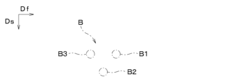
- a plurality of laser beams B with different irradiation positions PR in the scanning direction Ds and the line feed direction Df are applied to the ingot C surface by one laser scanning.
- 21 is irradiated.
- the irradiation positions PR on the ingot C surface 21 are arranged to be inclined with respect to both the scanning direction Ds and the line feed direction Df in plan view.
- a plurality of laser beams B (that is, the first beam B1, etc.) moves along the scanning direction Ds. Thereby, a plurality of scanning lines Ls are formed by one laser scanning. Therefore, the cycle time in the peeling layer forming process can be favorably shortened.
- FIGS. 4A, 4B, and 5A show an example of three laser beams B as the plurality of laser beams B.
- the plurality of laser beams B includes at least the first beam B1, the second beam B2 and the third beam B3.
- the first beam B1 is the most leading, that is, the first beam B1 is positioned closest to the scanning direction Ds.
- the third beam B3 is assumed to be the most trailing.
- the second beam B2 is positioned between the first beam B1 and the third beam B3 in the scanning direction Ds and the line feed direction Df.
- the first beam B1 travels in the scanning direction Ds ahead of the second beam B2.
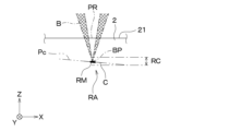
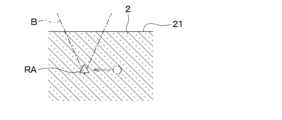
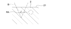
- an irradiation affected area RA is generated at a predetermined depth from the ingot C surface 21, which is the laser irradiation surface.
- the irradiation-affected region RA consists of an irradiation mark RM consisting of a modified region formed by separating SiC into Si and C by irradiation with the laser beam B, and the (0001) plane Pc from the irradiation mark RM around it. and a crack C extending along.
- the irradiation position PR of the second beam B2 may overlap at least the crack C in the irradiation affected area RA formed by the preceding first beam B1 in the in-plane direction. If the irradiation marks RM and cracks C included in the irradiation affected area RA by the preceding first beam B1 exist at the irradiation position PR of the following second beam B2, the absorption rate of the second beam B2 is changed by the irradiation affected area RA. increases. For this reason, the irradiation mark RM by the following second beam B2 is likely to occur at substantially the same depth as the depth of the irradiation affected area RA by the preceding first beam B1.
- FIG. 6 shows the trajectory of relative movement of the central position of the light collecting device 42 in the in-plane direction with respect to the ingot 2 .
- the “central position in the in-plane direction of the condensing device 42” is typically the central position in the arrangement of the multiple laser beams B, for example.
- the ingot 2 is oriented such that the facet region RF is positioned on the "lower off-angle side", and the laser beam B is directed from the C-plane side.
- the release layer forming step is performed by irradiation.
- the “lower off-angle side” refers to the lower inclination side of the C-plane, that is, the (0001) plane Pc when the orientation of the ingot 2 is set so that the C-plane 21 of the ingot, which is one principal plane, faces upward. shall be said.
- the “higher off-angle side” refers to the higher inclination side of the C-plane, that is, the (0001) plane Pc when the ingot 2 is oriented so that the C-plane 21 of the ingot faces upward. shall be
- the “higher off-angle side” of the ingot 2 is considered the hypothetical example of applying a unidirectional load at one end. In this respect, the edge of the ingot 2 adjacent to the facet region RF is less prone to cracking in the first place.
- the success rate of the wafer peeling process may decrease.
- the ingot 2 is oriented such that the facet region RF is positioned on the “lower off-angle side”, and after the laser beam B is irradiated from the C surface side, the ingot 2 is “off-angled”. A unidirectional load is applied at one end of the high corner.
- the separation starting position is a portion far from the facet region RF where cracks are relatively likely to occur. Therefore, according to this embodiment, the success rate of the wafer peeling process is improved.
- the laser beam B is applied to the ingot 2 so that the energy application density due to the laser beam B irradiation is higher in the facet region RF than in the non-facet region RN. Irradiate the main surface.
- the “energy application density” referred to here is the energy application density in the plane along the main surface of the ingot 2 .
- the following means can be used singly or in combination. Specifically, for example, the output of the laser beam B is made higher in the facet region RF than in the non-facet region RN.
- the main surface of the ingot 2 is irradiated with the laser beam B so that the facet region RF is irradiated with the laser beam B more frequently than the non-facet region RN.
- the repetition frequency of the laser beam B is set higher than that in the non-facet region RN, or the scanning speed is lowered while the repetition frequency is constant, and irradiation in the scanning direction Ds is performed. Close the gap.
- the output in the facet region RF is preferably 1.5 times the output in the non-facet region RN.
- the irradiation interval in the facet region RF should be 2/5 of the irradiation interval in the non-facet region RN.
- the facet region RF is irradiated with the laser beam B separately from the irradiation of the laser beam B onto the entire region including the facet region RF and the non-facet region RN.
- the laser beam B may also irradiate a region adjacent to the facet region RF in the non-facet region RN.
- the release layer 25 can be satisfactorily formed in the entire region including the facet region RF and the non-facet region RN.
- the separation layer 25 can be formed on the facet region RF without adjusting the distance in the Z-axis direction between the focusing device 42 on the irradiation side of the laser beam B and the chuck table 41 supporting the ingot 2. , can be done similarly to the non-faceted regions RN. Therefore, according to this embodiment, it is possible to improve the manufacturing efficiency more than the conventional one.
- forward scanning Sc1 in which the irradiation position PR when irradiated with the laser beam B moves on the main surface of the ingot 2 in the same direction as the off-angle direction D ⁇ ;
- a backward scan Sc2 occurs in which the irradiation position PR when the laser beam B is irradiated moves on the main surface of the ingot 2 in the direction opposite to the off-angle direction D ⁇ . That is, in forward scanning Sc1, the scanning direction Ds is the same as the off-angle direction D ⁇ . On the other hand, in the backward scanning Sc2, the scanning direction Ds is opposite to the off-angle direction D ⁇ .
- the forward scanning Sc1 and the backward scanning Sc2 are alternately performed.
- the relative position of the light collecting device 42 with respect to the ingot 2 moves by a predetermined amount in the line feed direction Df between the end of one forward scan Sc1 and the start of the next forward scan Sc1.
- the relative position of the light collecting device 42 in the line feed direction Df may move between the end of one forward scan Sc1 and the start of the backward scan Sc2 immediately thereafter. and do not need to move.
- the amount of relative movement in the line feed direction Df at each stage can be appropriately set according to the irradiation conditions of the laser beam B and the like.
- the laser beam B is irradiated over the entire width of the ingot 2 in the scanning direction Ds. That is, in the forward scan Sc1, the main surface of the ingot 2 is irradiated with the laser beam B while the irradiation position PR is moved on the main surface of the ingot 2 in the scanning direction Ds that is the same direction as the off-angle direction D ⁇ . Thereby, a scanning line Ls is formed between both ends of the ingot 2 in the scanning direction Ds.
- the laser beam B may be irradiated over the entire width of the ingot 2 in the scanning direction Ds, or the laser beam B may not be irradiated over the entire width of the ingot 2 in the scanning direction Ds. may Alternatively, in the backward scanning Sc2, the laser beam B may be irradiated not only on the entire width of the ingot 2 in the scanning direction Ds but on a part thereof.
- the laser beam B may be applied only to the facet region RF and its periphery. This makes it possible to form the release layer 25 satisfactorily over the entire region including the facet region RF and the non-facet region RN.
- the laser beam B may be applied only to the end of the ingot 2 in the scanning direction Ds.
- the irradiation position PR moves on the main surface of the ingot 2 in the scanning direction Ds, which is the direction opposite to the off-angle direction D ⁇ , a scanning line is formed on the end of the ingot 2 in the scanning direction Ds. Ls is formed.
- the laser beam B may be irradiated only to the facet region RF and its peripheral portion, and the end portion of the ingot 2 in the scanning direction Ds.
- the intensity of the laser beam B is increased at the peripheral edge portion outside the center portion in the beam radial direction, which is the direction radially extending from the center of the axis. intensity distribution.
- the laser beam B has a beam shape that is ring-shaped or hollow in front of the condensing point BP and converges into a point at the condensing point BP.
- the laser beam B has a condensed diameter dc, which is the minimum beam diameter.
- the intersection range RX shown in FIG. 7 is a predetermined range centered on the focal point BP in the beam axis direction in which the peripheral edges of the laser beam B having high intensity overlap each other.
- the release layer forming apparatus 40 irradiates the ingot 2 with the annular laser beam B.
- a ring-shaped laser beam B and an apparatus for generating such a laser beam B and irradiating it to a workpiece are already known or well-known at the time of filing of the present application (for example, Japanese Patent Application Laid-Open No. 2006-130691). Japanese Patent Laid-Open No. 2014-147946, etc.). For this reason, the detailed description of the generation device and generation method of the laser beam B is omitted in this specification.
- FIG. 8A shows how an irradiation affected area RA including an irradiation mark RM is formed by the annular laser beam B according to this embodiment.
- FIG. 8B shows, as another example different from the present embodiment, how an irradiation affected area RA including an irradiation mark RM is formed by a non-annular or solid laser beam B.
- irradiation marks RM which are modified regions formed by separating SiC into Si and C by irradiation with the laser beam B, are formed. , may occur at different depths than the focal point BP. Therefore, the depth of the irradiation affected area RA, which is composed of the irradiation marks RM and the cracks C developed from the irradiation marks RM, can also be different from the focal point BP. Specifically, for example, at a position shallower than the focal point BP, the energy application density due to the irradiation of the laser beam B may increase to such an extent that the irradiation mark RM can be generated.
- the irradiation mark RM can occur at a position shallower than the focal point BP.
- the depth of the irradiation mark RM may vary due to variations in the irradiation energy of the laser beam B, variations in the refractive index of the ingot 2, variations in the optical system of the light collecting device 42, and the like.
- a region in which irradiation marks RM may occur is shown as a modifiable range RC in the figure. Note that the irradiation mark RM corresponds to the “modified layer” in Patent Document 1.
- the energy application density due to the irradiation of the laser beam B increases to the extent that the irradiation mark RM can be generated.
- Limited to the depth near the focal point BP that is, for example, as in the case of using a solid laser beam B, the energy application density due to the irradiation of the laser beam B at a position shallower than the focal point BP increases to the extent that irradiation marks RM can be generated. becomes difficult. Therefore, the irradiation mark RM is stably generated at a depth near the focal point BP.
- the modifiable range RC is limited to a narrow depth range centered on the depth of the focal point BP. Therefore, variations in the depth of the irradiation mark RM can be suppressed satisfactorily.
- the peeling layer 25 can be formed as thin as possible, and the processing allowance in grinding and polishing after peeling can be favorably reduced. Therefore, according to this embodiment, it is possible to improve the manufacturing efficiency more than the conventional one.
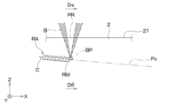
- the laser scanning direction is a direction orthogonal to "the direction in which the off-angle ⁇ is formed (that is, the off-angle direction D ⁇ in FIGS. 1 and 3A, etc.)". For this reason, cleavage is not stable, and material loss increases.
- the scanning direction Ds which is the moving direction of the focal point BP of the laser beam B inside the ingot 2
- the irradiation position PR is moved in the scanning direction Ds along the off-angle direction D ⁇ by laser scanning.
- the peeling layer forming device 40 scans the laser beam B by moving the light collecting device 42 relative to the ingot 2 in the scanning direction Ds parallel to the off-angle direction D ⁇ , thereby turning off the scanning line Ls. It is formed along the angular direction D ⁇ . Then, as shown in FIGS. 9 and 10, irradiation marks RM and cracks C are formed along the (0001) plane Pc. As a result, the cleavage of the peeling layer 25 during the wafer peeling process can be stabilized, and the material loss can be favorably reduced. Also, the processing allowance in the wafer flattening process can be favorably reduced, so that the process time can be shortened as much as possible. Therefore, according to this embodiment, it is possible to provide a wafer manufacturing method with higher manufacturing efficiency than the conventional one.
- FIG. 9 shows an example in which the scanning direction Ds is the same direction as the off-angle direction D ⁇ .
- FIG. 10 shows an example in which the scanning direction Ds is opposite to the off-angle direction D ⁇ . That is, in the example shown in FIG. 9, when the attitude of the ingot 2 is set so that the C surface 21 of the ingot faces upward as shown in FIG. , (0001) plane Pc from the high side to the low side. On the other hand, in the example shown in FIG. 10, when the attitude of the ingot 2 is set so that the C surface 21 of the ingot is the top surface, laser scanning causes the irradiation position PR to be a low point on the (0001) surface Pc. Move from the side to the high side.
- the current irradiation position PR usually has an irradiation affected area RA formed precedingly (for example, immediately before). Then, the absorptivity of the laser beam B increases in the irradiation affected area RA. Also, the irradiation affected area RA is formed along the (0001) plane Pc. Therefore, the laser scanning causes the irradiation mark RM to easily develop along the (0001) plane Pc.
- the irradiation mark RM is gradually formed at a deeper position by the laser scanning as it progresses in the scanning direction Ds along the (0001) plane Pc. Gradually move away from the light spot BP. Then, at a depth almost identical to that of the irradiation mark RM formed immediately before, the energy application density of the laser beam B to be irradiated this time may not be increased to the extent that a new irradiation mark RM can be generated. . In this case, the irradiation mark RM can no longer progress along the (0001) plane Pc. Then, as shown in FIG.
- a newly formed irradiation mark RM is formed at a depth near the focal point BP of the laser beam B irradiated this time. That is, a step occurs between the irradiation mark RM formed immediately before and the irradiation mark RM formed this time.
- the laser scanning causes the irradiation mark RM to be gradually formed at a shallower position as it progresses along the (0001) plane Pc in the scanning direction Ds. Gradually move away from point BP. At a depth almost identical to that of the irradiation mark RM formed immediately before, if the energy application density of the laser beam B irradiated this time is no longer increased to the extent that a new irradiation mark RM can be generated, irradiation will occur. The mark RM can no longer progress along the (0001) plane Pc. Then, as shown in FIG.
- a newly formed irradiation mark RM is formed at a depth near the focal point BP of the laser beam B irradiated this time.
- the direction in which the irradiation mark RM grows is the direction closer to the light source side of the laser beam B, that is, the laser-irradiated surface side of the ingot 2. . Therefore, in the example shown in FIG. 10, the irradiation mark RM tends to grow longer than in the example shown in FIG. Therefore, in the example shown in FIG. 10, the step between the previously formed irradiation mark RM and the currently formed irradiation mark RM is larger than in the example shown in FIG.
- the scanning direction Ds the same as the off-angle direction D ⁇ and moving the irradiation position PR in the laser scanning from the higher side toward the lower side of the C plane, the irradiation mark RM formed immediately before and the current irradiation mark RM It is possible to reduce the step between the formed irradiation marks RM. As a result, the peeling layer 25 can be formed as thin as possible, so that the processing allowance in grinding and polishing after peeling can be reduced satisfactorily. Therefore, according to this aspect, it is possible to further improve the manufacturing efficiency as compared with the conventional art.
- FIG. 11 schematically shows a wafer peeling process and a peeling apparatus 50 used in this process. It is assumed that the right-handed XYZ coordinates shown in FIG. 11 are displayed so as to match the right-handed XYZ coordinates shown in FIG.
- the peeling device 50 applies a load in one direction at the first end 23 , which is one end of the ingot 2 , in the in-plane direction parallel to the ingot C surface 21 , that is, the off-angle direction D ⁇ , thereby separating the wafer precursor 26 from the peeling layer 25 . It is configured to separate from the ingot 2 at .
- the first end 23 is the end on the “high side of the off-angle”, that is, the end on the high side of the C-plane, that is, the (0001) plane Pc when the ingot 2 is oriented so that the C-plane 21 of the ingot faces upward. is.
- the peeling device 50 applies a static and/or dynamic load in the Z-axis direction in the figure in such a manner as to separate the ingot C surface 21 from the ingot Si surface 22 at the first end 23. It is configured to be applied to the ingot 2 .
- the peeling device 50 includes a support table 51 , a peeling pad 52 , and a driving member 53 .
- the support table 51 is provided to support the ingot 2 from below. More specifically, the support table 51 has a large number of suction holes (not shown) that open on a support attraction surface 51a, which is the upper surface of the support table 51, so that the ingot Si surface 22 is attracted to the support attraction surface 51a by air pressure. is configured to The support table 51 has a first table end portion 51b and a second table end portion 51c, which are both end portions in the off-angle direction D ⁇ . A second table end portion 51c, which is an end portion on one side (that is, the left side in the drawing) in the off-angle direction D ⁇ , has a table base end surface 51d.
- the support table 51 d of table base end surfaces are formed in the shape of an inclined surface which rises toward the off-angle direction D(theta). That is, as shown in FIG. 11, the support table 51 is formed in a trapezoidal shape in which the lower base is longer than the upper base when viewed from the side.
- the stripping pad 52 is provided above the support table 51 so as to be able to approach and separate from the support table 51 along the Z axis in the figure. That is, the peeling device 50 is configured such that the support table 51 and the peeling pad 52 are relatively movable in the height direction of the ingot 2 .
- the stripping pad 52 has a large number of suction holes (not shown) that open at a pad adsorption surface 52a, which is the bottom surface of the stripping pad 52, and is configured to adsorb the ingot C surface 21 to the pad adsorption surface 52a by air pressure. .
- the peeling pad 52 has a first pad end portion 52b and a second pad end portion 52c, which are both ends in the off-angle direction D ⁇ .
- the second pad end portion 52c which is the end portion on one side (that is, the left side in the drawing) in the off-angle direction D ⁇ , has a pad end surface 52d.
- the pad end surface 52d is formed in an inclined surface shape that descends toward the off-angle direction D ⁇ . That is, as shown in FIG. 11, the stripping pad 52 is formed in a trapezoidal shape in which the lower base is shorter than the upper base when viewed from the side. 52 d of pad end surfaces are provided in the position corresponding to 51 d of table base end surfaces (that is, right above).
- the ingot C surface 21 is fixed to the peeling pad 52 by suction and the ingot Si surface 22 is fixed to the support table 51 by suction, so that the ingot 2 is sandwiched between the support table 51 and the peeling pad 52. , hereinafter referred to as a "sandwiched state".
- the drive member 53 applies an external force to at least one of the support table 51 and the stripping pad 52 to relatively move the support table 51 and the stripping pad 52 along the height direction of the ingot 2 in the clamping state. It is arranged to be applied to one side.
- the drive member 53 has a first drive end face 53a and a second drive end face 53b.
- the first drive end surface 53a is formed in an inclined surface shape that descends toward the off-angle direction D ⁇ . More specifically, the first drive end face 53a is provided parallel to the pad end face 52d.
- the second driving end surface 53b is formed in an inclined surface that rises toward the off-angle direction D ⁇ . More specifically, the second driving end surface 53b is provided parallel to the table base end surface 51d.
- the driving member 53 is provided so that the first driving end surface 53a contacts the pad end surface 52d and the second driving end surface 53b contacts the table base end surface 51d in the sandwiched state. That is, as shown in FIG. 11, the driving member 53 is formed in a trapezoidal shape whose lower base is longer than its upper base and which is rotated clockwise by 90 degrees when viewed from the side.
- the driving member 53 is configured to be driven upward along the height direction of the ingot 2 and/or in the off-angle direction D ⁇ , which is the direction toward the ingot 2, by a driving means (not shown).
- the driving member 53 is driven upward and/or in the off-angle direction D ⁇ to apply a moment to the ingot 2 with the second pad end 52c as the force FP and the first end 23 as the fulcrum PP and action point WP. designed to work.
- a wafer peeling process for peeling the wafer precursor 26 from the ingot 2 includes a table fixing process, a clamping process, and a peeling force applying process.
- the table fixing step is a step of fixing the ingot 2 to the support table 51 by adsorbing the ingot Si surface 22 to the support adsorption surface 51a.
- the sandwiching step is a step of attaching the ingot C surface 21 to the pad adsorption surface 52 a to fix the ingot 2 to the peeling pad 52 to form a sandwiched state.
- the second pad end which is the end of the peeling pad 52 on one side in the off-angle direction D ⁇ , is applied to the ingot 2 so that a moment with the first end 23 as the fulcrum PP acts on the ingot 2 in the sandwiched state.
- This is a step of applying a static or dynamic load using the portion 52c as the force point FP.
- the driving member 53 is driven upward and/or in the off-angle direction D ⁇ in the sandwiched state, thereby moving the second pad end portion 52 c upward along the height direction of the ingot 2 .
- the wafer peeling process is performed on the first end 23 which is one end of the ingot 2 in the in-plane direction parallel to the upper surface of the ingot 2 (that is, the ingot C surface 21 in the example of FIG. 11). by applying a load in one direction. Then, a moment with the first end 23 as the fulcrum PP and the action point WP acts on the ingot 2 .
- the point of action WP and the fulcrum PP are provided inside the ingot 2, that is, inside the outer edge of the peeling layer 25 in the in-plane direction.
- a much larger load than that of the present embodiment was required in order to cause good peeling with the peeling layer 25 as the interface.
- the position of the peeling crack may not be fixed, and a partial unpeeled portion or breakage of the removed wafer 1 may occur.
- the peeled cross-section becomes rough and the processing allowance for grinding and polishing increases. Therefore, in the comparative example, there is room for improvement in terms of load reduction, yield, and the like.
- a load is applied in one direction at one end of the ingot 2 in the off-angle direction D ⁇ . . That is, the load is concentrated on one end of the release layer 25 in the off-angle direction D ⁇ . Then, a moment having this one end as the fulcrum PP and the action point WP acts on the ingot 2 .
- the crack formed at the end of the ingot 2 on the one end side in the off-angle direction D ⁇ is the starting point, the delamination progresses, so that the fracture progresses stably over the entire surface of the delamination layer 25 while reducing the applied load.
- the present disclosure is not limited to the specific configurations shown in the above embodiments. That is, for example, the outer diameter and planar shape of the wafer 1, that is, the ingot 2 (for example, whether or not there is a so-called orientation flat) are not particularly limited.
- the magnitude of the off angle ⁇ is also not particularly limited.
- the wafer C-plane 11 and the ingot C-plane 21 do not coincide with the C-plane in the strict crystallographic sense, that is, the (0001) plane Pc.
- the term "C surface” is used because the term "C surface” is acceptable under social conventions.
- the present disclosure is not limited to such aspects. That is, the wafer C-plane 11 and the ingot C-plane 21 may coincide with the C-plane in the strict crystallographic sense, that is, the (0001) plane Pc.
- the off angle ⁇ may be 0 degrees.
- the irradiation conditions and scanning conditions of the laser beam B are not limited to the specific examples shown in the above embodiment. That is, for example, the arrangement of a plurality of laser beams B emitted in one laser scan can also be appropriately changed from the specific mode shown in FIG. 5A. Specifically, for example, as shown in FIG. 12, a first beam B1, a second beam B2, and a third beam are arranged at different positions with respect to the line feed direction Df (i.e., the second direction). B3 may be arranged in a V shape on the laser irradiation surface. More specifically, the first beam B1, the second beam B2 and the third beam B3 are arranged in this order along the line feed direction Df.
- the second beam B2 is provided at a position that protrudes in the scanning direction Ds from the first beam B1 and the third beam B3.
- the multiple laser beams B can be arranged in a W-shape or staggered pattern.
- the laser beam B is irradiated to the entire width of the ingot 2 in the scanning direction Ds in the backward scanning Sc2 as in the forward scanning Sc1
- the irradiation conditions for both may be different.
- the distance from the laser irradiation surface of the light collecting device 42 that is, the ingot C surface 21 (that is, the irradiation distance) may be changed between the forward scanning Sc1 and the backward scanning Sc2.
- the peeled surface 32 may have such a surface condition that it can be satisfactorily ground or polished even if it is subjected to the ECMG process as it is. Therefore, the rough grinding step of the peeled surface 32 shown in FIG. 2 may be omitted. The same applies to the rough grinding of the upper surface of the ingot 2 after the wafer peeling process.
- the release layer forming apparatus 40 shown in FIGS. 4A and 4B is a simplified schematic diagram for simply explaining the outline of the release layer forming process according to the present disclosure. Therefore, the specific configuration of the release layer forming apparatus 40 that is actually industrially implemented does not necessarily match the exemplary configuration shown in FIGS. 4A and 4B.
- the chuck table 41 may be configured to hold the ingot 2 by a method other than an air pressure adsorption mechanism. Also, the chuck table 41 may be configured to be relatively movable with respect to the light collector 42 at least in the in-plane direction, that is, in the XY directions in the figure.
- the peeling layer forming device 40 may include a scanning device configured to allow the focal point BP of the laser beam B to move relative to the ingot 2 in the XYZ directions in the drawing.
- the peeling layer forming apparatus 40 is configured such that the chuck table 41 that supports the ingot 2 is movable at least in the in-plane direction, while the light collecting device 42 is fixedly provided in the in-plane direction. had been
- the present disclosure is not limited to such aspects.
- the separation layer forming apparatus 40 has a configuration in which the chuck table 41 that supports the ingot 2 is fixed in the in-plane direction, while the light collecting device 42 is moved in the in-plane direction by a scanning device (not shown).
- a scanning device not shown
- the faceted region RF or the non-faceted region RN or regardless of this, the Z-axis between the condenser 42 on the irradiation side of the laser beam B and the chuck table 41 supporting the ingot 2 Making directional distance adjustments is optional for the purposes of this disclosure.
- the specific configuration of the release layer forming apparatus 40 that is actually industrially realized can be appropriately changed from the exemplary configuration shown in FIGS. 4A and 4B.
- the peeling layer 25 is formed on the C surface 21 side of the ingot by "irradiating the C surface 21 of the ingot with the laser beam B".
- the present disclosure is not limited to such aspects. That is, the present disclosure is also applicable to “Si surface side irradiation” in which the Si surface 22 of the ingot is irradiated with the laser beam B to form the separation layer 25 on the Si surface 22 side of the ingot.
- the peeling apparatus 50 shown in FIG. 11 is a simplified schematic diagram for simply explaining the outline of the wafer peeling process according to the present disclosure. Therefore, the specific configuration of the peeling device 50 that is actually industrially implemented does not necessarily match the exemplary configuration shown in FIG. 11 .
- the support table 51 may be configured to adsorb the ingot Si surface 22 to the support adsorption surface 51a using a method (for example, wax, adhesive, etc.) other than an air pressure adsorption mechanism. good.
- the optical properties that is, the transmittance and refractive index of the obtained wafer 1 or peeled body 30 are measured at a plurality of positions in the scanning direction Ds and the line feed direction Df, and the next irradiation of the laser beam B is performed based on the measurement results. Conditions may be controlled.
- FIG. 14 shows a schematic of such an embodiment.
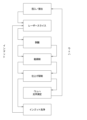
- "insertion/ejection” indicates the step of inserting and ejecting the stripped body 30 and the ingot 2, which are the workpieces.
- Laser slicing indicates a release layer forming step.
- Strip indicates a wafer stripping process.
- “Rough grinding” indicates a step of rough grinding the main surfaces of the ingot 2 and the peeled body 30 .
- abrasive For rough grinding, for example, it is possible to use an abrasive of about #800.
- “Finish grinding” indicates a process of finishing the surface.
- For the finish grinding for example, it is possible to use an abrasive of about #30000.
- “Wafer optical measurement” indicates a step of measuring the optical properties (that is, transmittance and refractive index) of the peeled body 30 that has undergone finish grinding at multiple positions in the scanning direction Ds and the line feed direction Df.
- Ingot cleaning indicates a process of cleaning the ingot 2 after finish grinding.
- the arrows on the left side of the block indicating each step indicate the flow of processing for the ingot 2
- the arrows on the right side indicate the flow of processing for the wafer 1 or the separated body 30, which can be commonly called a "wafer". .
- the ingot 2 is put into a wafer manufacturing apparatus including a peeling layer forming apparatus 40 .
- a peeling layer forming step is performed by irradiating the laser beam B to the ingot 2 that has been thrown.
- the peeling body 30 is peeled off from the ingot 2 that has undergone the peeling layer forming process.
- the upper surface of the ingot 2 newly produced in the ingot 2 that has undergone the wafer peeling process is flattened by rough grinding and finish grinding.
- the ingot 2 is subjected to the release layer forming step again after being washed.
- the ingot 2 that has undergone the separation layer forming process or the ingot cleaning process is ejected from the wafer manufacturing apparatus when the height thereof becomes less than a predetermined value.
- the stripped body 30 stripped from the ingot 2 by the wafer stripping process is subjected to rough grinding and finish grinding, and is subjected to optical measurement, that is, measurement of transmittance and refractive index.
- the measurement results are used to determine irradiation conditions (for example, irradiation energy and/or irradiation distance) of the laser beam B in the next release layer forming step. That is, based on the measurement results of the transmittance and refractive index for each location in the in-plane direction of the wafer 1, the irradiation conditions for each location in the in-plane direction of the ingot C surface 21 in the next peeling layer forming step are controlled. .
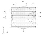
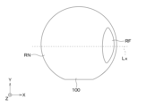
- FIG. 15 shows an example of how optical measurement positions are set in the generator 100 .
- the product 100 is an object of optical measurement, and corresponds to the stripped body 30 whose surface is flattened to a predetermined extent after being stripped from the wafer 1 or ingot 2 .
- the optical measurement positions are set at a constant pitch (eg, 3 mm) in each of the X-axis direction (ie first direction) and the Y-axis direction (ie second direction).
- the X-axis direction is parallel to the scanning direction Ds shown in FIG. 6 and the like.
- the Y-axis direction is parallel to the line feed direction Df shown in FIG. 6 and the like.
- the measurement line Lx is an imaginary straight line parallel to the X-axis passing through the center of the product 100 in the in-plane direction and the facet region RF.
- the absorption coefficient is obtained or calculated by the following formula (1).
- ⁇ represents the absorption coefficient
- D represents the thickness of the workpiece, that is, the thickness of the product 100
- T represents the transmittance.
- the horizontal axis indicates the measurement position when the center of the generated body 100 in the in-plane direction is the origin, that is, "0".
- the absorption coefficient is not constant in the in-plane direction, but changes as the measurement position changes.
- the region with a high absorption coefficient on the right end side in FIG. 17 corresponds to the facet region RF.
- a “radial direction” is a direction radially extending from the center of the in-plane direction of the generator 100 .
- FIGS. 18A to 18C show how the modified layer generation position changes as the transmittance, that is, the absorption coefficient changes.
- the position where the modified layer is generated is the position where the modified layer, that is, the irradiation affected area RA is generated by condensing the laser beam B. can be shown.
- the depth direction of the ingot 2 is a direction parallel to the height direction of the ingot 2, and more specifically, the direction opposite to the height direction of the ingot 2 (that is, the Z-axis negative direction in FIG. 1 and the like).
- the circle indicated by the dashed line beside the irradiation affected area RA indicates the condensing state of the laser beam B at the position where the modified layer is generated, ie, the beam diameter.
- the laser beam B is condensed while being attenuated according to the absorption coefficient as it travels in the depth direction of the ingot 2 .
- the processing threshold value is reached, and the modified layer, that is, the irradiation affected area RA is formed.
- the transmittance is low (that is, the absorption coefficient is high)
- the attenuation is large, so as shown in FIG. Reforming occurs when the energy density is reached.
- the transmittance is high (that is, the absorption coefficient is low)
- the attenuation is small. Therefore, as shown in FIG. is reached and reformation occurs.
- the modified layer generation position varies due to the difference in transmittance, that is, the absorption coefficient, the surface of the product 100 after peeling becomes rough, and the processing allowance for grinding and polishing, ie, the material loss increases.
- the transmittance is measured at multiple positions in the in-plane direction, and the irradiation conditions of the laser beam B are controlled at each of the multiple positions based on the measurement results.
- the absorption coefficient is obtained, that is, calculated based on the transmittance measured in the generated body 100 generated in the past including the previous time.
- the irradiation energy of the laser beam B is determined based on the change tendency of the absorption coefficient in the depth direction of the ingot 2 for each different position within the plane.
- the transmittance and the like of the product 100 obtained last time are measured using a transmittance measuring instrument.
- the workpiece thickness is also measured.
- the absorption coefficient is calculated based on the measured transmittance, the work thickness, and the above equation (1).
- the input energy which is the irradiation energy of the laser beam B, is derived using the following equation (2).
- I0 indicates the input energy
- I indicates the energy required at the processing point, that is, the minimum applied energy required for reforming
- z indicates the depth.
- k indicates the amount of change in the absorption coefficient in the depth direction, that is, the change tendency of the absorption coefficient in the depth direction of the ingot 2 .
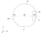
- the center of the ingot 2 in the in-plane direction is defined as the in-plane center position Ma.
- the end position of the ingot 2 on the measurement line Lx passing through the in-plane center position Ma and parallel to the X-axis and located within the facet region RF is defined as a first end position Mb.
- a position on the measurement line Lx and opposite to the first end position Mb is defined as a second end position Mc.
- the second end position Mc is a position substantially symmetrical to the first end position Mb with the in-plane center position Ma as the center.
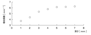
- FIG. 21A shows how the absorption coefficient changes in the depth direction of the ingot 2 at the in-plane center position Ma.
- FIG. 21B shows how the absorption coefficient changes in the depth direction of the ingot 2 at the first end position Mb.
- FIG. 21C shows how the absorption coefficient changes in the depth direction of the ingot 2 at the second end position Mc.
- the change in the absorption coefficient in the depth direction of the ingot 2 has a specific tendency and differs for each in-plane position. Based on the change tendency of the absorption coefficient in the depth direction for each in-plane position, the absorption coefficient change amount is derived, and the value obtained by adding or multiplying this to the absorption coefficient acquired last time is input for the next processing. It can be applied to the determination of energy.
- the absorption coefficient estimated value used for the current processing is It is possible to obtain or calculate ⁇ n .
- the difference between the absorption coefficient ⁇ n ⁇ 1 acquired last time and the absorption coefficient ⁇ n ⁇ 2 acquired last time before last is taken as the amount of change in absorption coefficient, and this is used as the absorption coefficient ⁇ n ⁇ acquired last time.
- the absorption coefficient estimate ⁇ n can be calculated.
- the irradiation energy of the laser beam B can be determined based on the estimated absorption coefficient ⁇ n .
- Statistical processing using a so-called “smoothing filter" or the like may be performed when calculating the amount of change in absorption coefficient.
- a first generator 101 and a second generator 102 are generated.
- the first product 101 is the product 100 obtained from one end side of the ingot 2 in the height direction, that is, the C surface 21 side of the ingot.
- the second product 102 is the product 100 obtained from the other end side of the ingot 2 in the height direction, that is, the side of the Si surface 22 of the ingot.
- the first absorption coefficient, which is the absorption coefficient in the first generated body 101, and the second absorption coefficient, which is the absorption coefficient in the second generated body 102 are acquired.
- the irradiation condition of the laser beam B that is, the irradiation energy
- the absorption coefficient obtained from the generator 100 having the higher absorption coefficient, ie, the wafer may be set as the upper limit, and the coefficient setting may be such that the absorption coefficient is not changed beyond that limit.
- the measurement pitch of optical measurement may be measured at an equal pitch as shown in FIG. 15, but it can be changed as appropriate. That is, for example, different pitches may be used in the X-axis direction and the Y-axis direction.
- the measurement pitch may be finer in a region such as a region surrounded by a rectangle with a dashed line in FIG. 24, where the change in absorption coefficient is greater than in other regions.
- Such an area is specifically, for example, a boundary area between the non-facet area RN and the facet area RF. That is, in such a boundary area, the measurement pitch may be finer than in other areas. Note that the region where the measurement pitch is made finer may include the entire facet region RF.
- the measurement pitch may be finer in the area where the measurement position is to the right of 40 mm than in the area where the measurement position is to the left of 40 mm.
- the measurement pitch may be finer in the predetermined area formed by the non-facet area RN and the boundary area between the non-facet area RN and the facet area RF than in the area outside the predetermined area.
- the laser beam B used in the experiment is a pulsed laser with a wavelength of 1064 nm, a pulse width of 7 ns, and an oscillation frequency of 25 kHz.
- Laser beam B is a ring-shaped beam with an outer diameter of 4.85 mm and an inner diameter of 2.82 mm.
- the laser beam B was made incident on a lens of NA 0.65, and processing was performed at an irradiation pitch (that is, an irradiation interval in the scanning direction Ds) of 8 ⁇ m and a scanning interval (that is, an interval between scanning lines Ls in the line feed direction Df) of 120 ⁇ m.
- the ingot 2 to be processed has an outer diameter of 6 inches and an in-plane absorption coefficient difference of 2.49 mm ⁇ 1 .
- the transmittance measurements were performed at a 3 mm pitch on the previously cut wafer 1 having a thickness of 0.385 mm.
- the input energy was set to an output setting in which an energy of 20 ⁇ J was input at a depth of 0.4 mm in the center of the ingot 2 .
- the height difference of the in-plane modification layer generation position was 61 ⁇ m.
- the height difference at the modified layer generation position was improved to 18 ⁇ m. It was shown that this can reduce material loss.
- Modifications are not limited to the above examples either. That is, for example, a plurality of embodiments other than those exemplified above can be combined with each other as long as they are not technically inconsistent. Likewise, multiple variants may be combined with each other unless technically inconsistent.
- a wafer manufacturing method for obtaining a wafer (1) from an ingot (2) comprising: A peeling layer (25) is formed from the surface to a depth corresponding to the thickness of the wafer by irradiating a surface (21) on one end side in the height direction of the ingot with a laser beam having transparency.
- the ingot is a single crystal SiC ingot having a c-axis (Lc) and a C-plane (Pc) perpendicular to each other,
- the c-axis is provided in a state in which the central axis (L) orthogonal to the surface is inclined in the off-angle direction (D ⁇ ) by an off-angle ( ⁇ ) exceeding 0 degrees,
- the release layer is formed so that the facet region is located on the lower side of the C-plane when the ingot is oriented so that the surface faces upward.
- the wafer peeling is performed by applying a load in one direction at one end (23) of the ingot in the off-angle direction.
- the one end of the ingot in the off-angle direction is the high end of the C-plane when the ingot is oriented so that the surface faces upward.
- the peeling layer is formed by laser scanning in which the surface is irradiated with the laser beam while moving the irradiation position (PR) of the laser beam on the surface along the first direction (Ds) along the surface.
- the peeling layer is formed by forming a plurality of scanning lines (Ls) along the second direction, when moving the irradiation position in the first direction, forming the scanning line between both ends of the surface in the first direction; When the irradiation position is moved in the direction opposite to the first direction, the irradiation mark is formed at the end of the surface in the first direction.
- the peeling layer is formed by laser scanning in which the surface is irradiated with the laser beam while moving the irradiation position (PR) of the laser beam on the surface along the first direction (Ds) along the surface.
- the peeling layer is formed by forming a plurality of scanning lines (Ls) along the second direction, When the irradiation position is moved in the first direction and when the irradiation position is moved in a direction opposite to the first direction, the above-mentioned Change the distance from the surface.
- the irradiation energy of the laser beam is determined based on the value obtained by adding or multiplying the absorption coefficient change amount to the absorption coefficient obtained last time.
- the irradiation energy of the laser beam is determined based on the absorption coefficient estimated value obtained based on the amount of change between the absorption coefficient obtained last time and the absorption coefficient obtained last time before.
- the measurement pitch of the transmittance is made finer than in the first region.
- the second area is a boundary area between the non-facet area (RN) and the facet area (RF).
Abstract
インゴット(2)からウェハを得るウェハ製造方法は、以下の手順、工程、あるいは処理を含む。インゴットの高さ方向における一端側の表面(21)に対して透過性を有するレーザービームを照射することで、表面からウェハの厚みに対応する深さに剥離層(25)を形成する。このとき、非ファセット領域(RN)よりもファセット領域(RF)の方が、照射頻度が高くなるように、レーザービームを照射する。インゴットの表面と剥離層との間の部分であるウェハ前駆体(26)を、剥離層にてインゴットから剥離する。インゴットからウェハ前駆体を剥離することで得られた板状の剥離体の主面を、電気化学的機械的に平坦化することで、ウェハを得る。
Description
本出願は、2021年12月8日に出願された日本特許出願番号2021-199577号および2022年8月10日に出願された日本特許出願番号2022-128100号に基づくもので、ここにそれらの記載内容が参照により組み入れられる。
本開示は、ウェハ製造方法に関する。
SiCの損失が比較的少ないSiCウェハの製造方法として、SiCに対して透過性を有する波長のレーザービームをSiC単結晶インゴットの内部に集光して改質層とこの改質層から伸長するクラックとを形成して割断する方法が知られている。この方法では、レーザービームの集光点をSiC単結晶インゴットの所定の深さ位置に位置付けて被割断面に沿ってレーザービームを走査し、この被割断面に沿って改質層を形成する。ところで、SiC単結晶は、その成長過程においてファセット領域と呼ばれる領域と、非ファセット領域と呼ばれる領域という、互いに成長モードが異なる領域が形成される。ファセット領域と、非ファセット領域とは、互いに透過率が異なる。このため、SiCに対して透過性を有する波長のレーザービームをSiC単結晶インゴットの表面から所定の深さに照射して改質層を形成しようとする際、ファセット領域と非ファセット領域とでは、改質層が形成される閾値を超えるエネルギー密度に達する深さが異なってしまう。この点、ファセット領域と非ファセット領域とでレーザービームの吸収性が異なること、具体的には、非ファセット領域はファセット領域よりもレーザービームの吸収性が低いことを開示している文献がある。また、同文献は、集光点に到達するレーザービームの強度は、ファセット領域よりも非ファセット領域の方が強くなることを開示している。そして、同文献は、ファセット領域と非ファセット領域とのそれぞれに適した条件でSiCに対して透過性を有するレーザービームを照射すると、SiC単結晶インゴットの所定の深さ位置に一様な改質層を形成できることを開示している。
上記の通り、ファセット領域よりも非ファセット領域の方が集光点に到達するレーザービームの強度が強くなることや、ファセット領域と非ファセット領域とのそれぞれに適した条件でレーザービームを照射することについては、公知文献に開示がある。しかしながら、同文献には、照射条件をどのように制御すればよいかについては、何ら開示されていない。一方、特許文献1は、加工送り工程において、ファセット領域にレーザービームを照射する際にレーザービームのエネルギーを上昇させると共に集光器の位置を上昇させる技術を開示している。「加工送り工程」とは、以下のような工程である。SiCに対して透過性を有する波長のレーザー光線の集光点を、SiCインゴットの上面から生成すべきウェハの厚みに相当する深さに位置づける。レーザー加工装置の集光器からレーザー光線をSiCインゴットに照射しながら、SiCインゴットと集光点とをX軸方向に相対的に加工送りして、SiCがSiとCとに分離すると共にc面に沿ってクラックが伸長した帯状の剥離層を形成する。しかしながら、かかる技術においても、集光器を上昇させるのには一定の応答遅れが生じ、高速にレーザービームを走査した際には追従できない。また、集光器を上下することで振動が発生し、改質層の深さがばらつくことで、材料ロスが増大してしまう。
本開示は、上記に例示した事情等に鑑みてなされたものである。すなわち、本開示は、例えば、ファセット領域と非ファセット領域とを含む全領域に対して剥離層を良好に形成することで、従来よりも製造効率を高くすることが可能なウェハ製造方法を提供する。
本開示は、上記に例示した事情等に鑑みてなされたものである。すなわち、本開示は、例えば、ファセット領域と非ファセット領域とを含む全領域に対して剥離層を良好に形成することで、従来よりも製造効率を高くすることが可能なウェハ製造方法を提供する。
本開示の1つの観点によれば、ウェハ製造方法は、インゴットからウェハを得る方法であって、
前記インゴットの高さ方向における一端側の表面に対して透過性を有するレーザービームを照射することで、前記表面から前記ウェハの厚みに対応する深さに剥離層を形成する、剥離層形成と、
前記表面と前記剥離層との間の部分であるウェハ前駆体を、前記剥離層にて前記インゴットから剥離する、ウェハ剥離と、
前記ウェハ剥離により得られた板状の剥離体の主面を平坦化する、ウェハ平坦化と、
を含み、
前記剥離層形成は、非ファセット領域よりもファセット領域の方が、照射頻度が高くなるように、前記レーザービームを前記表面に照射する。
前記インゴットの高さ方向における一端側の表面に対して透過性を有するレーザービームを照射することで、前記表面から前記ウェハの厚みに対応する深さに剥離層を形成する、剥離層形成と、
前記表面と前記剥離層との間の部分であるウェハ前駆体を、前記剥離層にて前記インゴットから剥離する、ウェハ剥離と、
前記ウェハ剥離により得られた板状の剥離体の主面を平坦化する、ウェハ平坦化と、
を含み、
前記剥離層形成は、非ファセット領域よりもファセット領域の方が、照射頻度が高くなるように、前記レーザービームを前記表面に照射する。
かかるウェハ製造方法においては、まず、前記インゴットの前記高さ方向における前記一端側の前記表面に対して透過性を有する前記レーザービームを照射することで、前記表面から前記ウェハの厚みに対応する深さに前記剥離層を形成する。次に、前記インゴットの前記表面と前記剥離層との間の部分である前記ウェハ前駆体を、前記剥離層にて前記インゴットから剥離する。続いて、前記インゴットから前記ウェハ前駆体を剥離することで得られた板状の前記剥離体の前記主面を平坦化することで、前記ウェハを得る。
ここで、上記の通り、前記ファセット領域よりも前記非ファセット領域の方が、集光点に到達する前記レーザービームの強度が強くなる。そこで、前記剥離層を形成する際、前記非ファセット領域よりも前記ファセット領域の方が、照射頻度が高くなるように、前記レーザービームを前記表面に照射する。具体的には、例えば、前記ファセット領域にて、前記非ファセット領域よりも、前記レーザービームの繰り返し周波数を高くして、前記第一方向における照射間隔を狭くする。あるいは、例えば、前記ファセット領域にて、前記非ファセット領域よりも、前記レーザービームの前記第二方向における照射間隔を狭くする。あるいは、例えば、前記ファセット領域と前記非ファセット領域とを含む全領域に対する前記レーザービームの照射とは別に、前記ファセット領域に対する前記レーザービームの照射を行う。かかるウェハ製造方法によれば、前記ファセット領域と前記非ファセット領域とを含む全領域に対して、前記剥離層を良好に形成することが可能となる。したがって、かかるウェハ製造方法によれば、従来よりも製造効率を高めることが可能となる。
なお、出願書類中の各欄において、各要素に括弧付きの参照符号が付されている場合がある。この場合、参照符号は、同要素と後述する実施形態に記載の具体的構成との対応関係の単なる一例を示すものである。よって、本開示は、参照符号の記載によって、何ら限定されるものではない。
(実施形態)
以下、本開示の実施形態を、図面に基づいて説明する。なお、一つの実施形態に対して適用可能な各種の変形例については、当該実施形態に関する一連の説明の途中に挿入されると、当該実施形態の理解が妨げられるおそれがある。このため、変形例については、当該実施形態に関する一連の説明の途中には挿入せず、その後にまとめて説明する。
以下、本開示の実施形態を、図面に基づいて説明する。なお、一つの実施形態に対して適用可能な各種の変形例については、当該実施形態に関する一連の説明の途中に挿入されると、当該実施形態の理解が妨げられるおそれがある。このため、変形例については、当該実施形態に関する一連の説明の途中には挿入せず、その後にまとめて説明する。
(ウェハおよびインゴットの構造)
図1を参照すると、本実施形態に係るウェハ製造方法によって製造されるウェハ1は、側面視にて略円柱状のインゴット2をスライスして得られるものであって、平面視にて略円形の薄板状に形成されている。すなわち、ウェハ1およびインゴット2は、中心軸Lを囲む略円柱面状の側面あるいは端面を有している。中心軸Lは、ウェハ1やインゴット2の、略円柱面状の側面あるいは端面と平行で、ウェハ1やインゴット2の軸中心を通る仮想直線である。なお、図示および説明の簡略化の観点から、ウェハ1やインゴット2に通常設けられる、いわゆるオリエンテーションフラットについては、本明細書においては、図示および説明を省略する。
図1を参照すると、本実施形態に係るウェハ製造方法によって製造されるウェハ1は、側面視にて略円柱状のインゴット2をスライスして得られるものであって、平面視にて略円形の薄板状に形成されている。すなわち、ウェハ1およびインゴット2は、中心軸Lを囲む略円柱面状の側面あるいは端面を有している。中心軸Lは、ウェハ1やインゴット2の、略円柱面状の側面あるいは端面と平行で、ウェハ1やインゴット2の軸中心を通る仮想直線である。なお、図示および説明の簡略化の観点から、ウェハ1やインゴット2に通常設けられる、いわゆるオリエンテーションフラットについては、本明細書においては、図示および説明を省略する。
本実施形態においては、インゴット2は、互いに直交するc軸Lcと(0001)面Pcとを有する単結晶SiCインゴットであって、0度を超えるオフ角θを有している。c軸Lcは、方向指数により[0001]として示される結晶軸である。(0001)面Pcは、c軸Lcと直交する、結晶学上厳密な意味で「C面」と称される結晶面である。オフ角θは、ウェハ1あるいはインゴット2の中心軸Lとc軸Lcとのなす角であって、例えば1~4度程度である。すなわち、ウェハ1およびインゴット2におけるc軸Lcは、中心軸Lをオフ角方向Dθに0度を超えるオフ角θ傾けた状態で設けられている。オフ角方向Dθは、中心軸Lとc軸Lcとの交点を中心として中心軸Lをc軸Lcに向かって回転させた場合の、ウェハ1やインゴット2におけるレーザー照射面(すなわち図中上面あるいは頂面)側に位置する中心軸L上の点の移動方向を、当該レーザー照射面に写像した方向である。
説明の簡略化のため、図1に示した通りに右手系XYZ座標を設定する。かかる右手系XYZ座標において、オフ角方向DθとX軸正方向とは、同一方向であるものとする。また、X軸およびY軸は、ウェハ1およびインゴット2の主面と平行であるものとする。「主面」は、板状物における板厚方向と直交する表面であって、「上面」や「底面」あるいは「板面」とも称され得る。あるいは、「主面」は、インゴット2のような柱状物における高さ方向と直交する表面であって、「頂面」あるいは「底面」とも称され得る。さらに、ウェハ1の厚さ方向およびインゴット2の高さ方向と、Z軸とが平行であるものとする。Z軸と直交する任意の方向を、以下「面内方向」と称することがある。
ウェハ1は、一対の主面であるウェハC面11およびウェハSi面12を有している。本実施形態においては、ウェハ1は、上面であるウェハC面11が(0001)面Pcに対してオフ角θ傾くように形成されている。同様に、インゴット2は、一対の主面であるインゴットC面21およびインゴットSi面22を有している。インゴット2は、頂面であるインゴットC面21が(0001)面Pcに対してオフ角θ傾くように形成されている。以下、インゴット2のオフ角方向Dθにおける一端すなわち上流端を第一端23と称し、他端すなわち下流端を第二端24と称する。なお、図1においては、ウェハC面11およびインゴットC面21が向く方向が、Z軸正方向として示されている。
また、インゴット2は、ファセット領域RFを有している。ファセット領域RFは、「ファセット部」とも称され得る。インゴット2におけるファセット領域RF以外の部分を、以下、非ファセット領域RNと称する。同様に、非ファセット領域RNは、「非ファセット部」とも称され得る。
(ウェハ製造方法の概略)
本実施形態に係るウェハ製造方法は、インゴット2からウェハ1を得る方法であって、以下の工程を含む。
本実施形態に係るウェハ製造方法は、インゴット2からウェハ1を得る方法であって、以下の工程を含む。
(1)剥離層形成工程:インゴット2の高さ方向における一端側の主面であるインゴットC面21に対して、インゴット2に対する所定程度の透過性を有するレーザービームを照射することで、インゴットC面21からウェハ1の厚みに対応する深さに剥離層25を形成する。
ここで、「所定程度の透過性」とは、インゴット2の内側におけるウェハ1の厚みに対応する深さにレーザービームの集光点を形成することが可能な程度の透過性である。また、「ウェハ1の厚みに対応する深さ」は、完成品であるウェハ1の厚み(すなわち厚みの狙い値)に、後述するウェハ平坦化工程等における所定の加工代に相当する厚みを加算した寸法であって、「ウェハ1の厚みに相当する深さ」とも称され得る。
ここで、「所定程度の透過性」とは、インゴット2の内側におけるウェハ1の厚みに対応する深さにレーザービームの集光点を形成することが可能な程度の透過性である。また、「ウェハ1の厚みに対応する深さ」は、完成品であるウェハ1の厚み(すなわち厚みの狙い値)に、後述するウェハ平坦化工程等における所定の加工代に相当する厚みを加算した寸法であって、「ウェハ1の厚みに相当する深さ」とも称され得る。
(2)ウェハ剥離工程:レーザー照射面であるインゴットC面21と剥離層25との間の部分であるウェハ前駆体26を、剥離層25にてインゴット2から剥離する。
ここで、上記の「ウェハ剥離工程」という表現の如く、インゴット2からウェハ前駆体26を剥離することで得られた板状物は、社会通念上「ウェハ」と称されることがあり得る。しかしながら、エピレディに鏡面化された主面を有する製造後の最終的なウェハ1と区別するため、かかる板状物を、以下、「剥離体30」と称する。
剥離体30は、一対の主面である、非剥離面31および剥離面32を有している。非剥離面31は、ウェハ剥離工程前において剥離層25を構成していなかった側の面であって、剥離層形成工程やウェハ剥離工程を行う前におけるインゴットC面21に対応する面である。剥離面32は、ウェハ剥離工程前において剥離層25を構成しており、ウェハ剥離工程によって新たに生じた表面である。剥離面32は、剥離層25およびウェハ剥離工程による剥離に起因する、粗い(すなわち研削あるいは研磨が必要な程度の)凹凸を有している。
(3)ウェハ平坦化工程:剥離体30の主面である非剥離面31および剥離面32のうちの、少なくとも剥離面32を平坦化することで、製造後の最終的なウェハ1を得る。ウェハ平坦化工程においては、一般的な砥石研磨やCMPに加えて、ECMGやECMPを用いることが可能である。なお、CMPはChemical Mechanical Polishingの略である。ECMGはElectro-Chemical Mechanical Grindingの略である。ECMPはElectro-Chemical Mechanical Polishingの略である。ウェハ平坦化工程は、これらの複数種類の平坦化工程を、単独で、あるいは、適宜組み合わせることで行われ得る。
(4)インゴット平坦化工程:ウェハ前駆体26を剥離した後に、新たに生じた、インゴット2の上面を、剥離層形成工程に再度供することができるように、平坦化すなわち鏡面化する。インゴット平坦化工程においても、一般的な砥石研磨やCMPに加えて、ECMGやECMPを用いることが可能である。インゴット平坦化工程も、これらの複数種類の平坦化工程を、単独で、あるいは、適宜組み合わせることで行われ得る。
図2は、本実施形態に係るウェハ製造方法を具体化した典型的な一例を示す工程図である。図2に示されているように、剥離層形成工程およびウェハ剥離工程を経てインゴット2から剥離された剥離体30は、以下の工程を経て、エピレディなウェハ1に仕上げられる。
・ウェハSi面12となるべき剥離面32の粗研削
・粗研削を経た剥離面32のECMG研削
・ECMG研削を経た剥離面32のECMP研磨
・洗浄
・ウェハSi面12となるべき剥離面32の粗研削
・粗研削を経た剥離面32のECMG研削
・ECMG研削を経た剥離面32のECMP研磨
・洗浄
また、剥離層形成工程およびウェハ剥離工程を経てインゴット2から剥離体30が剥離された後に残ったインゴット2は、以下の工程を経て、再度の剥離層形成工程に供され得る。
・ウェハ剥離工程により新たに生じたインゴットC面21の粗研削
・粗研削を経たインゴットC面21の仕上げ研削
・洗浄
・ウェハ剥離工程により新たに生じたインゴットC面21の粗研削
・粗研削を経たインゴットC面21の仕上げ研削
・洗浄
以下、各工程の詳細について、図1および図2に加えて他の図をも用いつつ説明する。
(剥離層形成工程)
図3Aおよび図3Bは、剥離層形成工程により剥離層25およびウェハ前駆体26が形成された状態のインゴット2の概略構成を示す。図4Aおよび図4Bは、剥離層形成工程の概略、および、かかる工程に用いられる剥離層形成装置40の概略構成を示す。なお、図3Aないし図4Bに示された右手系XYZ座標は、図1に示された右手系XYZ座標と整合するように表示されているものとする。
図3Aおよび図3Bは、剥離層形成工程により剥離層25およびウェハ前駆体26が形成された状態のインゴット2の概略構成を示す。図4Aおよび図4Bは、剥離層形成工程の概略、および、かかる工程に用いられる剥離層形成装置40の概略構成を示す。なお、図3Aないし図4Bに示された右手系XYZ座標は、図1に示された右手系XYZ座標と整合するように表示されているものとする。
図3Aおよび図3Bを参照すると、X軸に沿った線状のレーザービームの照射痕である走査ラインLsをY軸方向に複数形成することにより、剥離層25が形成されている。走査ラインLsは、インゴット2に対するレーザービームの照射痕RMが線状に形成されたものである。本実施形態においては、走査ラインLsは、オフ角方向Dθに沿って設けられている。そして、複数の走査ラインLsは、ラインフィード方向Dfに配列されている。ラインフィード方向Dfは、オフ角方向Dθと直交する面内方向である。すなわち、ラインフィード方向Dfは、オフ角方向Dθと直交し、且つ、インゴット2の高さ方向と直交する方向である。
図4Aおよび図4Bを参照すると、剥離層形成装置40は、チャックテーブル41と、集光装置42とを備えている。チャックテーブル41は、インゴット2を、その底面であるインゴットSi面22側にて保持するように構成されている。具体的には、例えば、チャックテーブル41は、インゴットSi面22を空気圧等により吸着する吸着機構等を備えている。なお、後述するように、チャックテーブル41に対するインゴット2の固定方法は、かかる態様に限定されない。集光装置42は、不図示のパルスレーザー発振器が発振したレーザービームBを、チャックテーブル41に固定された被加工物であるインゴット2に照射するように、レーザービームBの照射方向であるビーム軸方向についてチャックテーブル41に対向配置されている。すなわち、集光装置42は、インゴット2の上面であるインゴットC面21側からレーザービームBをインゴット2に照射するように設けられている。具体的には、集光装置42は、インゴット2の内側における、インゴットC面21からウェハ1の厚みに対応する深さに、レーザービームBの集光点BPを形成するように構成されている。集光装置42は、「集光器」とも称され得るものであって、レーザービームBの集光点BPを所定位置に形成するための光学要素(例えばレンズ)を備えている。剥離層形成装置40は、レーザービームBの集光点BPを、インゴット2に対して、少なくとも面内方向すなわち図中XY方向に相対移動可能に構成されている。ここで、「面内方向」は、インゴット2の上面であるインゴットC面21と平行な方向となる。
剥離層形成装置40は、レーザービームBをインゴットC面21上にて走査方向Ds(すなわち第一方向)に走査する「レーザー走査」により、走査方向Dsに沿って走査ラインLsを形成する。すなわち、「レーザー走査」は、レーザー照射面であるインゴットC面21上におけるレーザービームBの照射位置PRを、走査方向Dsに移動させつつ、レーザービームBをインゴットC面21に対して照射することである。本実施形態においては、走査方向Dsは、オフ角方向Dθに沿った方向、具体的には、オフ角方向Dθと同一方向あるいはその反対方向である。そして、剥離層形成装置40は、レーザー走査をラインフィード方向Df(すなわち第二方向)について位置を変えつつ複数回行い、走査ラインLsをラインフィード方向Dfに沿って複数形成することで、剥離層25を形成する。ラインフィード方向Dfおよび走査方向Dsは、ともに、面内方向(すなわちインゴットC面21に沿った方向)であって、互いに直交する方向である。
本実施形態においては、剥離層形成装置40は、インゴット2を載置したチャックテーブル41を集光装置42に対して走査方向Dsに相対移動させてレーザービームBをインゴットC面21上で走査することで、走査ラインLsを走査方向Dsに沿って形成する。また、剥離層形成装置40は、1回のレーザー走査を実行した後、チャックテーブル41を、集光装置42に対してラインフィード方向Dfに沿って所定量相対移動させる。そして、剥離層形成装置40は、再度、走査方向Ds(すなわち前回のレーザー走査の際と同一あるいは反対の方向)にチャックテーブル41を集光装置42に対して相対移動させてレーザービームBを走査することで走査ラインLsを形成する。このようにして、剥離層形成装置40は、ラインフィード方向Dfにおけるほぼ全幅に亘って、レーザービームBを走査することで、走査ラインLsをラインフィード方向Dfに沿って複数形成する。このようにして、ラインフィード方向Dfに沿って複数設けられた走査ラインLsによって剥離層25が形成される。また、剥離層25よりもインゴットC面21側に、将来的にウェハ1となるべきウェハ前駆体26が形成される。なお、上記の通り、本実施形態においては、集光装置42が面内方向について固定的に設けられている一方、インゴット2を支持するチャックテーブル41が不図示の電動ステージ装置等の走査装置によって少なくとも面内方向に移動するように設けられている。一方、後述するように、本開示は、かかる態様に限定されない。すなわち、例えば、インゴット2を支持するチャックテーブル41が面内方向について固定的に設けられる一方、集光装置42が不図示の走査装置によって面内方向について可動に設けられるという実施態様もあり得る。しかしながら、これらいずれの態様においても、見掛け上、レーザービームBやその照射位置PRがインゴット2の主面上を面内方向に移動したり、レーザービームBやその集光点BPがインゴット2内を面内方向に移動したりするように見える。したがって、説明の簡略化のため、以下、レーザービームBやその照射位置PRがインゴット2の主面上を面内方向に移動したり、レーザービームBやその集光点BPがインゴット2内を面内方向に移動したりするような説明をすることがある。しかしながら、後述するように、本開示は、かかる態様に限定されない。
本実施形態は、図4Aおよび図4Bに示されているように、1回のレーザー走査にて、走査方向Dsおよびラインフィード方向Dfにおける照射位置PRが異なる複数のレーザービームBを、インゴットC面21に照射する。具体的には、図5Aおよび図5Bに示されているように、インゴットC面21上の照射位置PRが平面視にて走査方向Dsおよびラインフィード方向Dfの双方に対して傾斜して配列する複数のレーザービームB(すなわち第一ビームB1等)が、走査方向Dsに沿って移動する。これにより、1回のレーザー走査にて、走査ラインLsが複数形成される。したがって、剥離層形成工程におけるサイクルタイムが良好に短縮され得る。
なお、図4A、図4B、および図5Aにおいては、複数のレーザービームBとして、レーザービームBが3本の例が図示されている。しかしながら、これは、図示の簡略化上の都合によるものであって、レーザービームBの本数については特段の限定はない。但し、説明を簡略化するため、以下、複数のレーザービームBとして、第一ビームB1と第二ビームB2と第三ビームB3とが少なくとも含まれるものとして、説明を続行する。第一ビームB1と第二ビームB2と第三ビームB3とのうち、第一ビームB1は、最も先行する、すなわち、最も走査方向Ds側に位置するものとする。一方、第三ビームB3は、最も後行するものとする。そして、第二ビームB2は、走査方向Dsおよびラインフィード方向Dfについて、第一ビームB1と第三ビームB3との間に位置するものとする。
図5Aに示されているように、第一ビームB1は、第二ビームB2に先行して、走査方向Dsに進行する。第一ビームB1の照射により、図5Bに示されているように、照射影響領域RAが、レーザー照射面であるインゴットC面21から所定の深さに発生する。照射影響領域RAは、レーザービームBの照射によりSiCがSiとCとに分離することで形成される改質領域からなる照射痕RMと、かかる照射痕RMからその周囲に(0001)面Pcに沿って伸長するクラックCとを含む。このため、第二ビームB2の照射位置PRは、先行する第一ビームB1により形成された照射影響領域RAにおける、少なくともクラックCと、面内方向について重なることがあり得る。先行する第一ビームB1による照射影響領域RAに含まれる照射痕RMやクラックCが、後行する第二ビームB2の照射位置PRに存在すると、かかる照射影響領域RAにより第二ビームB2の吸収率が高まる。このため、先行する第一ビームB1による照射影響領域RAの深さとほぼ同一の深さに、後行する第二ビームB2による照射痕RMが発生しやすくなる。第二ビームB2と第三ビームB3との関係についても同様である。よって、1回のレーザー走査にて第一ビームB1~第三ビームB3により一度に形成される、ラインフィード方向Dfについて隣接する3つの照射痕RMあるいは照射影響領域RAは、ほぼ同じ深さに発生しやすくなる。すなわち、ラインフィード方向Dfについて隣接する、剥離層25を構成する複数の走査ラインLsが、ほぼ同じ深さに発生しやすくなる。
このように、本実施形態においては、剥離層25を構成する照射痕RMすなわち走査ラインLsの深さのばらつきが、可能な限り抑制され得る。これにより、剥離層25での剥離によって発生する剥離面32における段差や凹凸の大きさが良好に抑制され、剥離面32における研削や研磨の加工代が低減されたり、剥離不良の発生が良好に抑制されたりする。また、剥離層25を形成する際のサイクルタイムが短縮され得る。したがって、本実施形態によれば、従来よりも製造効率を高めることが可能となる。
図6は、集光装置42の面内方向における中心位置の、インゴット2に対する相対移動の軌跡を示す。「集光装置42の面内方向における中心位置」は、典型的には、例えば、複数のレーザービームBの配列における中心位置である。図4Aおよび図6に示されているように、本実施形態は、インゴット2の姿勢を、ファセット領域RFが「オフ角の低い側」に位置するようにして、レーザービームBをC面側から照射することで、剥離層形成工程を行う。「オフ角の低い側」とは、インゴット2の姿勢を、一主面であるインゴットC面21が上面となるように設定した場合の、C面すなわち(0001)面Pcにおける傾斜の低い側をいうものとする。これに対し、「オフ角の高い側」とは、インゴット2の姿勢を、インゴットC面21が上面となるように設定した場合の、C面すなわち(0001)面Pcにおける傾斜の高い側をいうものとする。
後述する通り、インゴット2における「オフ角の高い側」の一端にて、ウェハ前駆体26をインゴット2から剥離するための一方向荷重を印加することで、極めて良好なウェハ剥離が実現される。ここで、ファセット領域RFが「オフ角の高い側」に位置するようにインゴット2の姿勢を設定してレーザービームBをSi面側から照射した後、インゴット2における「オフ角の高い側」の一端にて一方向荷重を印加する想定例について考察する。この点、インゴット2における、ファセット領域RFに近接する端部は、そもそも亀裂が入りにくい。よって、かかる想定例においては、剥離開始位置が、亀裂が入りにくいファセット領域RFに近接する端部となるため、ウェハ剥離工程の成功率が低くなる可能性がある。これに対し、本実施形態は、インゴット2の姿勢を、ファセット領域RFが「オフ角の低い側」に位置するようにして、レーザービームBをC面側から照射した後、インゴット2における「オフ角の高い側」の一端にて一方向荷重を印加する。この場合、剥離開始位置が、亀裂が比較的入りやすい、ファセット領域RFから遠い部分となる。したがって、本実施形態によれば、ウェハ剥離工程の成功率が向上する。
ところで、ファセット領域RFよりも非ファセット領域RNの方が、集光点BPに到達するレーザービームBの強度が強くなることが知られている。そこで、本実施形態においては、剥離層形成工程において、非ファセット領域RNよりもファセット領域RFの方が、レーザービームBの照射によるエネルギーの印加密度が高くなるように、レーザービームBをインゴット2の主面に照射する。ここにいう「エネルギーの印加密度」は、インゴット2の主面に沿った面内におけるエネルギーの印加密度である。以下の手段が、単独で、あるいは、複合して用いられ得る。具体的には、例えば、ファセット領域RFにて、非ファセット領域RNよりも、レーザービームBの出力を高くする。あるいは、例えば、非ファセット領域RNよりもファセット領域RFの方がレーザービームBの照射頻度が高くなるように、レーザービームBをインゴット2の主面に照射する。より詳細には、例えば、ファセット領域RFにて、非ファセット領域RNよりも、レーザービームBの繰り返し周波数を高くする、もしくは繰り返し周波数が一定の状態で走査速度を低くして、走査方向Dsにおける照射間隔を狭くする。出力をファセット領域RFにて非ファセット領域RNよりも高くするにあたり、ファセット領域RFにおける出力は、非ファセット領域RNにおける出力の1.5倍が望ましい。走査方向Dsあるいはラインフィード方向Dfにおける照射間隔をファセット領域RFにて非ファセット領域RNよりも狭くするにあたり、ファセット領域RFにおける照射間隔は、非ファセット領域RNにおける照射間隔の2/5であることが好ましい。あるいは、例えば、ファセット領域RFと非ファセット領域RNとを含む全領域に対するレーザービームBの照射とは別に、ファセット領域RFに対するレーザービームBの照射を行う。なお、このファセット領域RFに対するレーザービームBの照射に際しては、非ファセット領域RNにおける、ファセット領域RFに近接する領域に対しても、レーザービームBが照射され得る。
本実施形態に係る剥離層形成工程によれば、ファセット領域RFと非ファセット領域RNとを含む全領域に対して、剥離層25を良好に形成することが可能となる。特に、レーザービームBの照射側の集光装置42と、インゴット2を支持するチャックテーブル41との間の、Z軸方向の距離調整を用いなくても、ファセット領域RFに対する剥離層25の形成が、非ファセット領域RNと同様に行われ得る。したがって、本実施形態によれば、従来よりも製造効率を高めることが可能となる。
図4Aおよび図6を参照すると、剥離層形成工程においては、レーザービームBを照射した場合の照射位置PRがインゴット2の主面上をオフ角方向Dθと同一方向に移動する往路走査Sc1と、レーザービームBを照射した場合の照射位置PRがインゴット2の主面上をオフ角方向Dθとは反対方向に移動する復路走査Sc2とが生じる。すなわち、往路走査Sc1においては、走査方向Dsがオフ角方向Dθと同一方向となる。これに対し、復路走査Sc2においては、走査方向Dsがオフ角方向Dθとは反対方向となる。往路走査Sc1と復路走査Sc2とは、交互に行われる。
1回の往路走査Sc1が終了してから、次回の往路走査Sc1が開始するまでの間に、集光装置42のインゴット2に対する相対位置が、ラインフィード方向Dfに所定量移動する。但し、1回の往路走査Sc1が終了してから、その直後に行われる復路走査Sc2が開始するまでの間については、集光装置42のラインフィード方向Dfにおける相対位置は、移動してもよいし、移動しなくてもよい。1回の復路走査Sc2が終了してから、引き続き行われる往路走査Sc1が開始するまでの間についても同様である。各段階における、ラインフィード方向Dfの相対移動量については、レーザービームBの照射条件等により適宜設定され得る。
往路走査Sc1においては、レーザービームBが、走査方向Dsにおけるインゴット2の全幅に亘って照射される。すなわち、往路走査Sc1においては、照射位置PRをインゴット2の主面上にてオフ角方向Dθと同一方向である走査方向Dsに移動させつつ、レーザービームBをインゴット2の主面に照射する。これにより、インゴット2の走査方向Dsにおける両端部の間にわたって走査ラインLsが形成される。これに対し、復路走査Sc2においては、走査方向Dsにおけるインゴット2の全幅に亘ってレーザービームBを照射してもよいし、走査方向Dsにおけるインゴット2の全幅に亘ってレーザービームBを照射しなくてもよい。あるいは、復路走査Sc2においては、走査方向Dsにおけるインゴット2の全幅ではなくその一部にレーザービームBを照射してもよい。
具体的には、例えば、復路走査Sc2においては、ファセット領域RFおよびその周辺部に対してのみ、レーザービームBを照射してもよい。これにより、ファセット領域RFと非ファセット領域RNとを含む全領域に対して、剥離層25を良好に形成することが可能となる。あるいは、例えば、復路走査Sc2においては、走査方向Dsにおけるインゴット2の端部にのみレーザービームBを照射してもよい。この場合、復路走査Sc2においては、照射位置PRがインゴット2の主面上にてオフ角方向Dθと反対方向である走査方向Dsに移動しつつ、インゴット2の走査方向Dsにおける端部に走査ラインLsが形成される。これにより、ウェハ剥離工程における剥離開始が良好に促進され、ウェハ剥離工程の成功率が向上する。また、復路走査Sc2においては、ファセット領域RFおよびその周辺部と、走査方向Dsにおけるインゴット2の端部とに対してのみ、レーザービームBを照射してもよい。
図7に示されているように、本実施形態においては、レーザービームBは、その軸中心から放射状に延びる方向であるビーム径方向における中心部よりも外側の周縁部にて強度が高くなるような強度分布を有している。具体的には、レーザービームBは、集光点BPの手前側にて環状すなわち中空状となる一方で、集光点BPにて点状に集光するビーム形状を有している。集光点BPにて、レーザービームBは、最小のビーム径である集光径dcを有している。図7に示された交差範囲RXは、レーザービームBにおける強度が高い周縁部同士の重なりが生じる、ビーム軸方向について集光点BPを中心とした所定範囲である。
このように、剥離層形成装置40は、環状のレーザービームBを、インゴット2に照射する。このような環状のレーザービームBや、かかるレーザービームBを生成して被加工物に照射する装置については、本願の出願時点で既に公知あるいは周知となっている(例えば、特開2006-130691号公報、特開2014-147946号公報、等参照。)。このため、かかるレーザービームBの生成装置や生成方法の詳細については、本明細書においては、説明を省略する。
図8Aは、本実施形態に係る環状のレーザービームBによって照射痕RMを含む照射影響領域RAが形成される様子を示す。図8Bは、本実施形態とは異なる別例として、非環状すなわち中実のレーザービームBによって照射痕RMを含む照射影響領域RAが形成される様子を示す。
図8Bに示されているように、中実のレーザービームBを用いた場合、レーザービームBの照射によりSiCがSiとCとに分離することで形成される改質領域である照射痕RMが、集光点BPとは異なる深さに発生し得る。このため、照射痕RMと、かかる照射痕RMから進展したクラックCとからなる照射影響領域RAの深さも、集光点BPとは異なる深さとなり得る。具体的には、例えば、集光点BPよりも浅い位置にて、レーザービームBの照射によるエネルギーの印加密度が、照射痕RMを発生させ得る程度にまで高まることがあり得る。すると、照射痕RMは、集光点BPよりも浅い位置に発生し得る。照射痕RMの発生深さは、レーザービームBの照射エネルギーのばらつきや、インゴット2の屈折率のばらつきや、集光装置42における光学系のばらつき等により変動し得る。照射痕RMが発生し得る領域を、図中、改質可能範囲RCとして示す。なお、照射痕RMは、特許文献1における「改質層」に相当する。
これに対し、図8Aに示されているように、環状のレーザービームBを用いた場合、レーザービームBの照射によるエネルギーの印加密度が、照射痕RMを発生させ得る程度にまで高まるのは、集光点BPの付近の深さに限定される。すなわち、例えば、中実のレーザービームBを用いた場合のように、集光点BPよりも浅い位置にてレーザービームBの照射によるエネルギーの印加密度が照射痕RMを発生させ得る程度にまで高まることは困難となる。よって、照射痕RMは、集光点BPの付近の深さに、安定的に発生する。すなわち、改質可能範囲RCは、中実のレーザービームBを用いた場合とは異なり、集光点BPの深さを中心とした狭い深さ範囲に限定される。このため、照射痕RMの発生深さのばらつきが、良好に抑制され得る。換言すれば、剥離層25を可能な限り薄く形成することが可能となり、剥離後の研削や研磨における加工代が、良好に低減され得る。したがって、本実施形態によれば、従来よりも製造効率を高めることが可能となる。
ところで、特許文献1に記載の方法は、レーザー走査方向が、「オフ角θが形成される方向(すなわち図1や図3A等におけるオフ角方向Dθ)」と直交する方向である。このため、へき開が安定せず、材料ロスが増大する。これに対し、本実施形態においては、図4Aに示されているように、インゴット2の内部におけるレーザービームBの集光点BPの移動方向である走査方向Dsは、オフ角方向Dθと平行である。すなわち、剥離層形成工程は、レーザー走査にて、照射位置PRを、オフ角方向Dθに沿った走査方向Dsに移動させる。換言すれば、剥離層形成装置40は、オフ角方向Dθと平行な走査方向Dsに集光装置42をインゴット2に対して相対移動させてレーザービームBを走査することで、走査ラインLsをオフ角方向Dθに沿って形成する。すると、図9および図10に示されているように、照射痕RMおよびクラックCが、(0001)面Pcに沿って形成される。これにより、ウェハ剥離工程時の剥離層25における、へき開を安定化させることができ、材料ロスが良好に低減される。また、ウェハ平坦化工程における加工代が良好に削減され、以て、工程時間が可能な限り短縮され得る。したがって、本実施形態によれば、従来よりも製造効率の高いウェハ製造方法を提供することが可能となる。
図9は、走査方向Dsがオフ角方向Dθと同一方向である例を示す。図10は、走査方向Dsがオフ角方向Dθとは反対方向である例を示す。すなわち、図9に示された例においては、図4Aに示されているように、インゴットC面21が上面となるようにインゴット2の姿勢を設定した場合、レーザー走査にて、照射位置PRを、(0001)面Pcにおける高い側から低い側に向かって移動させる。これに対し、図10に示された例においては、インゴットC面21が上面となるようにインゴット2の姿勢を設定した場合、レーザー走査にて、照射位置PRを、(0001)面Pcにおける低い側から高い側に向かって移動させる。
例えば、面内方向における照射位置PRの周囲に、照射影響領域RAすなわち照射痕RMやクラックCが存在しない状況を仮定する。かかる状況においては、レーザービームBの照射によって、照射痕RMは、集光点BP付近の深さに発生しやすい。一方、実際は、レーザービームBは、照射痕RMおよびクラックCを次々と生成しつつ、走査方向Dsに移動する。このため、上記のような状況は、主として、1回のレーザー走査において最初に形成される、走査ラインLsの始点に対応する照射痕RMの形成時にて発生する。よって、レーザー走査中のほとんどの場面において、面内方向における照射位置PRの周囲に照射影響領域RAが存在する状況が発生する。
すなわち、図9や図10に示されているように、現在の照射位置PRには、通常、先行して(例えば直前に)形成された照射影響領域RAが存在する。すると、かかる照射影響領域RAにて、レーザービームBの吸収率が高まる。また、かかる照射影響領域RAは、(0001)面Pcに沿って形成される。このため、レーザー走査により、照射痕RMは、(0001)面Pcに沿って進展しやすい。
ここで、図9に示された例においては、レーザー走査により、照射痕RMは、(0001)面Pcに沿って走査方向Dsに進展する際に、次第に深い位置に形成されることで、集光点BPから次第に離れる。すると、直前に形成された照射痕RMとほぼ同一の深さでは、今回照射されるレーザービームBによるエネルギーの印加密度が、新たな照射痕RMを発生させ得る程度にまで高められなくなることがある。この場合、照射痕RMは、これ以上(0001)面Pcに沿って進展することができなくなる。すると、図9に示されているように、新たに形成される照射痕RMは、今回照射されるレーザービームBにおける集光点BP付近の深さに形成される。すなわち、直前に形成された照射痕RMと、今回形成される照射痕RMとの間で、段差が生じる。
一方、図10に示された例においては、レーザー走査により、照射痕RMは、(0001)面Pcに沿って走査方向Dsに進展する際に、次第に浅い位置に形成されることで、集光点BPから次第に離れる。そして、直前に形成された照射痕RMとほぼ同一の深さでは、今回照射されるレーザービームBによるエネルギーの印加密度が、新たな照射痕RMを発生させ得る程度にまで高められなくなると、照射痕RMがこれ以上(0001)面Pcに沿って進展できなくなる。すると、図10に示されているように、新たに形成される照射痕RMは、今回照射されるレーザービームBにおける集光点BP付近の深さに形成される。但し、図10に示された例においては、図9に示された例とは異なり、照射痕RMの進展方向は、レーザービームBの光源側すなわちインゴット2のレーザー照射面側により近づく方向である。よって、図10に示された例においては、図9に示された例よりも、照射痕RMがより長く進展しやすくなる。したがって、図10に示された例においては、図9に示された例よりも、直前に形成された照射痕RMと今回形成される照射痕RMとの間で生じる段差が大きくなる。
このように、走査方向Dsをオフ角方向Dθと同一方向として、レーザー走査における照射位置PRをC面における高い側から低い側に向かって移動させることで、直前に形成された照射痕RMと今回形成される照射痕RMとの間の段差を小さくすることができる。これにより、剥離層25を可能な限り薄く形成することが可能となり、以て、剥離後の研削や研磨における加工代が、良好に低減され得る。したがって、かかる態様によれば、従来よりも製造効率をよりいっそう高めることが可能となる。
(ウェハ剥離工程)
図11は、ウェハ剥離工程、および、かかる工程に用いられる剥離装置50の概略を示す。なお、図11に示された右手系XYZ座標は、図1に示された右手系XYZ座標と整合するように表示されているものとする。
図11は、ウェハ剥離工程、および、かかる工程に用いられる剥離装置50の概略を示す。なお、図11に示された右手系XYZ座標は、図1に示された右手系XYZ座標と整合するように表示されているものとする。
剥離装置50は、インゴットC面21と平行な面内方向すなわちオフ角方向Dθにおけるインゴット2の一端である第一端23にて一方向に荷重を加えることで、ウェハ前駆体26を剥離層25にてインゴット2から剥離するように構成されている。第一端23は、「オフ角の高い側」の端、すなわち、インゴット2の姿勢をインゴットC面21が上面となるように設定した場合のC面すなわち(0001)面Pcにおける高い側の端である。本実施形態においては、剥離装置50は、第一端23にて、インゴットC面21をインゴットSi面22から引き離すような態様の図中Z軸方向の静的および/または動的な荷重を、インゴット2に対して印加するように構成されている。具体的には、本実施形態においては、剥離装置50は、支持テーブル51と、剥離パッド52と、駆動部材53とを備えている。
支持テーブル51は、インゴット2を下方から支持するように設けられている。具体的には、支持テーブル51は、その上面である支持吸着面51aにて開口する不図示の多数の吸引孔を有していて、空気圧によって支持吸着面51aにインゴットSi面22を吸着するように構成されている。支持テーブル51は、オフ角方向Dθにおける両端部である第一テーブル端部51bおよび第二テーブル端部51cを有している。オフ角方向Dθにおける一方側(すなわち図中左側)の端部である第二テーブル端部51cは、テーブル基端面51dを有している。テーブル基端面51dは、オフ角方向Dθに向かうにつれて上昇する傾斜面状に形成されている。すなわち、支持テーブル51は、図11に示されているように、側面視にて、上底よりも下底の方が長い台形状に形成されている。
剥離パッド52は、支持テーブル51の上方にて、支持テーブル51に対して図中Z軸に沿って接近および離隔自在に設けられている。すなわち、剥離装置50は、支持テーブル51と剥離パッド52とがインゴット2の高さ方向に相対移動可能に構成されている。剥離パッド52は、その底面であるパッド吸着面52aにて開口する不図示の多数の吸引孔を有していて、空気圧によってパッド吸着面52aにインゴットC面21を吸着するように構成されている。剥離パッド52は、オフ角方向Dθにおける両端部である第一パッド端部52bと第二パッド端部52cとを有している。オフ角方向Dθにおける一方側(すなわち図中左側)の端部である第二パッド端部52cは、パッド端面52dを有している。パッド端面52dは、オフ角方向Dθに向かうにつれて下降する傾斜面状に形成されている。すなわち、剥離パッド52は、図11に示されているように、側面視にて、上底よりも下底の方が短い台形状に形成されている。パッド端面52dは、テーブル基端面51dに対応する位置(すなわち真上)に設けられている。インゴットC面21が吸着により剥離パッド52に固定され且つインゴットSi面22が吸着により支持テーブル51に固定されることで、インゴット2が支持テーブル51と剥離パッド52との間で挟持された状態を、以下「挟持状態」と称する。
駆動部材53は、挟持状態にて、支持テーブル51と剥離パッド52とをインゴット2の高さ方向に沿って相対移動させるような外力を、支持テーブル51と剥離パッド52とのうちの少なくともいずれか一方に印加するように設けられている。具体的には、駆動部材53は、第一駆動端面53aと第二駆動端面53bとを有している。第一駆動端面53aは、オフ角方向Dθに向かうにつれて下降する傾斜面状に形成されている。より詳細には、第一駆動端面53aは、パッド端面52dと平行に設けられている。第二駆動端面53bは、オフ角方向Dθに向かうにつれて上昇する傾斜面状に形成されている。より詳細には、第二駆動端面53bは、テーブル基端面51dと平行に設けられている。また、駆動部材53は、挟持状態にて、第一駆動端面53aがパッド端面52dに当接するとともに第二駆動端面53bがテーブル基端面51dに当接するように設けられている。すなわち、駆動部材53は、図11に示されているように、側面視にて、上底よりも下底の方が長い台形を時計回りに90度回転させた形状に形成されている。そして、駆動部材53は、不図示の駆動手段により、インゴット2の高さ方向に沿った上方、および/または、インゴット2に接近する方向であるオフ角方向Dθに駆動されるように構成されている。すなわち、駆動部材53は、上方および/またはオフ角方向Dθに駆動されることで、第二パッド端部52cを力点FPとし第一端23を支点PPおよび作用点WPとするモーメントをインゴット2に作用させるように設けられている。
ウェハ前駆体26をインゴット2から剥離するウェハ剥離工程は、テーブル固定工程と、挟持工程と、剥離力印加工程とを含む。テーブル固定工程は、インゴットSi面22を支持吸着面51aに吸着することでインゴット2を支持テーブル51に固定する工程である。挟持工程は、インゴットC面21をパッド吸着面52aに吸着してインゴット2を剥離パッド52に固定することで挟持状態を形成する工程である。剥離力印加工程は、挟持状態にて、第一端23を支点PPとするモーメントがインゴット2に作用するように、オフ角方向Dθにおける一方側の剥離パッド52の端部である第二パッド端部52cを力点FPとして静的あるいは動的な荷重を印加する工程である。具体的には、剥離力印加工程は、挟持状態にて駆動部材53を上方および/またはオフ角方向Dθに駆動することで、第二パッド端部52cをインゴット2の高さ方向に沿った上方に押圧する工程である。これにより、剥離層25を界面として、インゴット2の一部であるウェハ前駆体26をインゴット2から剥離することができる。
このように、本実施形態においては、ウェハ剥離工程は、インゴット2の上面(すなわち図11の例においてはインゴットC面21)と平行な面内方向におけるインゴット2の一端である第一端23にて、一方向に荷重を加えることで行う。すると、第一端23を支点PPおよび作用点WPとするモーメントがインゴット2に作用する。
この点、特許第6678522号公報に記載のウェハ剥離工程においては、作用点WPや支点PPが、インゴット2の内部、すなわち、面内方向における剥離層25の外縁よりも内側に設けられていた。かかる比較例では、剥離層25を界面とする良好な剥離を発生させるために、本実施形態よりもはるかに大きな荷重が必要となっていた。また、剥離層25の広域に荷重が付与されるため、剥離亀裂位置が定まらず、部分的な未剥離部や、取り出されたウェハ1における破損が発生することがあった。さらに、剥離断面が粗くなり、研削や研磨の加工代が大きくなるという課題があった。したがって、比較例においては、低荷重化、歩留まり、等の点で、改善の余地があった。
これに対し、本実施形態に係るウェハ剥離工程においては、ウェハ前駆体26を剥離層25にてインゴット2から剥離するために、オフ角方向Dθにおけるインゴット2の一端にて一方向に荷重を加える。すなわち、荷重を、オフ角方向Dθにおける剥離層25の一端に集中させる。すると、かかる一端を支点PPおよび作用点WPとするモーメントがインゴット2に作用する。これにより、オフ角方向Dθにおけるインゴット2の一端側の端部に形成された亀裂を起点に剥離が進行するため、付与荷重を低減しつつ剥離層25の全面にて安定的に破断を進行させることができる。また、破断発生箇所を安定的に設定することで、剥離後に生じる剥離体30における剥離面32やインゴットC面21の表面粗さを低減することが可能となる。特に、破断発生の始点となる第一端23を、オフ角方向Dθにおける「オフ角の高い側」の一端とすることで、破断がスムーズに発生するとともに、へき開がよりいっそう安定化する。このため、ウェハ剥離工程における不良発生率や、ウェハ剥離工程後のインゴット2や剥離体30の研削や研磨における加工代が、良好に低減され得る。したがって、本実施形態によれば、従来よりも製造効率の高いウェハ製造方法を提供することが可能となる。
(変形例)
本開示は、上記実施形態に限定されるものではない。故に、上記実施形態に対しては、適宜変更が可能である。以下、代表的な変形例について説明する。以下の変形例の説明においては、上記実施形態との相違点を主として説明する。また、上記実施形態と変形例とにおいて、互いに同一または均等である部分には、同一符号が付されている。したがって、以下の変形例の説明において、上記実施形態と同一の符号を有する構成要素に関しては、技術的矛盾または特段の追加説明なき限り、上記実施形態における説明が適宜援用され得る。
本開示は、上記実施形態に限定されるものではない。故に、上記実施形態に対しては、適宜変更が可能である。以下、代表的な変形例について説明する。以下の変形例の説明においては、上記実施形態との相違点を主として説明する。また、上記実施形態と変形例とにおいて、互いに同一または均等である部分には、同一符号が付されている。したがって、以下の変形例の説明において、上記実施形態と同一の符号を有する構成要素に関しては、技術的矛盾または特段の追加説明なき限り、上記実施形態における説明が適宜援用され得る。
本開示は、上記実施形態にて示された具体的な構成に限定されない。すなわち、例えば、ウェハ1すなわちインゴット2の外径や平面形状(例えばいわゆるオリエンテーションフラットの有無等)についても、特段の限定はない。オフ角θの大きさについても、特段の限定はない。また、上記実施形態においては、ウェハC面11や、インゴットC面21は、厳密な結晶学的意味でのC面すなわち(0001)面Pcとは一致しない。しかしながら、このような場合であっても、「C面」と称することが社会通念上許容されているため、「C面」という表現を用いている。但し、本開示は、かかる態様に限定されない。すなわち、ウェハC面11や、インゴットC面21は、厳密な結晶学的意味でのC面すなわち(0001)面Pcと一致していてもよい。換言すれば、オフ角θは、0度であってもよい。
レーザービームBの照射条件や走査条件についても、上記実施形態にて示された具体例に限定されない。すなわち、例えば、1回のレーザー走査にて照射される複数のレーザービームBの配置も、図5Aに示された具体的態様から適宜変容され得る。具体的には、例えば、図12に示されているように、ラインフィード方向Df(すなわち第二方向)について互いに異なる位置に配置された、第一ビームB1、第二ビームB2、および第三ビームB3は、レーザー照射面上にて、V字状に配列されてもよい。より詳細には、第一ビームB1、第二ビームB2、および第三ビームB3は、この順に、ラインフィード方向Dfに沿って配置される。そして、第二ビームB2は、第一ビームB1および第三ビームB3よりも、走査方向Dsについて突出した位置に設けられる。換言すれば、図13に示されているように、複数のレーザービームBは、W字状あるいは千鳥状に配列され得る。このような複数のレーザービームBの配置によれば、前に加工した改質層により発生するへき開の長さよりも広い間隔で次の改質層を形成することで、へき開と改質層の干渉を抑制することが可能となる。また、例えば、復路走査Sc2においても往路走査Sc1と同様に走査方向Dsにおけるインゴット2の全幅にレーザービームBを照射する場合、両者の照射条件を異ならせてもよい。具体的には、例えば、往路走査Sc1と復路走査Sc2とで、集光装置42のレーザー照射面すなわちインゴットC面21からの距離(すなわち照射距離)を変更してもよい。
レーザービームBの照射条件や走査条件によっては、剥離面32は、そのままECMG工程に供されても良好に研削あるいは研磨され得る程度の表面状態を有している可能性がある。このため、図2に示された、剥離面32の粗研削工程は、省略される可能性がある。ウェハ剥離工程後のインゴット2の上面の粗研削についても同様である。
図4Aや図4Bに示された剥離層形成装置40は、本開示に係る剥離層形成工程の概要を簡易に説明するための、簡素化された概略図である。したがって、実際に工業上実現される剥離層形成装置40の具体的な構成は、必ずしも、図4Aや図4Bに示された例示的な構成と一致するとは限らない。具体的には、例えば、チャックテーブル41は、空気圧による吸着機構以外の方式で、インゴット2を保持するように構成されていてもよい。また、チャックテーブル41は、集光装置42に対して、少なくとも面内方向すなわち図中XY方向に相対移動可能に構成されていてもよい。あるいは、剥離層形成装置40は、レーザービームBの集光点BPをインゴット2に対して図中XYZ方向に相対移動可能に構成された走査装置を備えていてもよい。あるいは、上記実施形態においては、剥離層形成装置40は、インゴット2を支持するチャックテーブル41が少なくとも面内方向について移動可能に構成される一方、集光装置42が面内方向について固定的に設けられていた。しかしながら、本開示は、かかる態様に限定されない。すなわち、例えば、剥離層形成装置40は、インゴット2を支持するチャックテーブル41が面内方向について固定的に設けられる一方、集光装置42が不図示の走査装置によって面内方向に移動するという構成であってもよい。また、ファセット領域RFか非ファセット領域RNかに応じて、あるいは、これにかかわらず、レーザービームBの照射側の集光装置42と、インゴット2を支持するチャックテーブル41との間の、Z軸方向の距離調整を行うことは、本開示においては、任意事項である。その他、実際に工業上実現される剥離層形成装置40の具体的な構成は、図4Aや図4Bに示された例示的な構成から適宜変更され得る。
上記実施形態においては、レーザービームBをインゴットC面21に照射する「C面側照射」により、剥離層25をインゴットC面21側に形成した。しかしながら、本開示は、かかる態様に限定されない。すなわち、本開示は、レーザービームBをインゴットSi面22に照射して、剥離層25をインゴットSi面22側に形成する、「Si面側照射」に対しても適用可能である。
図11に示された剥離装置50は、本開示に係るウェハ剥離工程の概要を簡易に説明するための、簡素化された概略図である。したがって、実際に工業上実現される剥離装置50の具体的な構成は、必ずしも、図11に示された例示的な構成と一致するとは限らない。具体的には、例えば、支持テーブル51は、空気圧による吸着機構以外の方式(例えばワックスや接着剤等)を用いて、支持吸着面51aにインゴットSi面22を吸着するように構成されていてもよい。
得られたウェハ1あるいは剥離体30の、光学特性すなわち透過率や屈折率を、走査方向Dsおよびラインフィード方向Dfにおける複数位置にて測定し、かかる測定結果に基づいて次回のレーザービームBの照射条件を制御してもよい。図14は、かかる態様の概略を示す。図中、「投入/排出」は、被加工物である剥離体30やインゴット2の投入および排出の工程を示す。「レーザースライス」は、剥離層形成工程を示す。「剥離」は、ウェハ剥離工程を示す。「粗研削」は、インゴット2や剥離体30の主面を粗研削する工程を示す。粗研削は、例えば、#800程度の番手の研削材を用いることが可能である。「仕上げ研削」は、表面を仕上げ研削する工程を示す。仕上げ研削は、例えば、#30000程度の番手の研削材を用いることが可能である。「ウェハ光学測定」は、仕上げ研削を経た剥離体30の光学特性(すなわち透過率や屈折率)を、走査方向Dsおよびラインフィード方向Dfにおける複数位置にて測定する工程を示す。「インゴット洗浄」は、仕上げ研削後のインゴット2を洗浄する工程を示す。各工程を示すブロックの左側の矢印は、インゴット2の処理の流れを示し、右側の矢印は、ウェハ1、あるいは、社会通念上「ウェハ」と称され得る剥離体30の、処理の流れを示す。
図14を参照すると、まず、インゴット2が、剥離層形成装置40を含むウェハ製造装置に投入される。次に、投入されたインゴット2に対して、レーザービームBの照射による剥離層形成工程が行われる。続いて、ウェハ剥離工程にて、剥離層形成工程を経たインゴット2から剥離体30が剥離される。ウェハ剥離工程を経たインゴット2にて新たに生じた、インゴット2の上面は、粗研削および仕上げ研削により平坦化される。その後、インゴット2は、洗浄された後、剥離層形成工程に再度供される。なお、剥離層形成工程あるいはインゴット洗浄工程を経たインゴット2は、高さが所定値未満となった場合、ウェハ製造装置から排出される。
ウェハ剥離工程によりインゴット2から剥離された剥離体30は、粗研削および仕上げ研削を経て、光学測定すなわち透過率および屈折率の測定に供される。測定結果は、次回の剥離層形成工程におけるレーザービームBの照射条件(例えば照射エネルギーおよび/または照射距離)の決定に供される。すなわち、ウェハ1の面内方向における場所毎の透過率および屈折率の測定結果に基づいて、次回の剥離層形成工程でのインゴットC面21の面内方向における場所毎の照射条件が制御される。これにより、面内方向における場所毎の光学特性のバラツキに対応した、きめ細かな照射条件の変更が可能となり、以て材料ロスを低減することが可能となる。特に、インゴット2がファセット領域RFを有する場合に有効である。なお、透過率および屈折率の測定は、いずれか一方のみであってもよい。あるいは、透過率および屈折率の測定は、最終的に得られたエピレディなウェハ1に対して行ってもよい。また、粗研削の条件によっては(例えばECMGの場合は)、仕上げ研削は不要となり得る。すなわち、粗研削と仕上げ研削とは、統合され得る。
図15は、生成体100における光学測定位置の設定態様の一例を示す。生成体100は、光学測定の対象であって、ウェハ1、あるいは、インゴット2から剥離された後に表面が所定程度平坦化された剥離体30に相当する。この例においては、光学測定位置は、X軸方向(すなわち第一方向)およびY軸方向(すなわち第二方向)のそれぞれについて、一定ピッチ(例えば3mm)で設定されている。X軸方向は、図6等に示されている走査方向Dsと平行である。また、Y軸方向は、図6等に示されているラインフィード方向Dfと平行である。ここで、図16に示されているように、測定線Lx上の複数の測定位置にて光学測定した場合の、測定位置の変化に伴うレーザービームBの吸収係数の変化の様子を、図17に示す。測定線Lxは、生成体100の面内方向における中心とファセット領域RFとを通りX軸と平行な仮想直線である。吸収係数は、下記(1)式によって、取得すなわち算出される。下記(1)式において、αは吸収係数を示し、Dはワーク厚さすなわち生成体100の厚さを示し、Tは透過率を示す。

図17において、横軸は、生成体100の面内方向における中心を原点すなわち「0」としたときの、測定位置を示す。図17に示されているように、吸収係数は、面内方向について一定ではなく、測定位置の変化に伴い変化する。具体的には、図17における右端側の、吸収係数が高い領域は、ファセット領域RFに相当する。また、ファセット領域RFよりも吸収係数が低い非ファセット領域RNにおいても、面内方向すなわち径方向についての分布を有する。「径方向」は、生成体100の面内方向における中心から放射状に延びる方向である。具体的には、図17の例では、中心位置よりも左側すなわち外側にて、吸収係数が低い領域が存在する。
図18A~図18Cは、透過率すなわち吸収係数の変化に伴う、改質層発生位置の変化の様子を示す。改質層発生位置は、レーザービームBの集光により改質層すなわち照射影響領域RAが発生する位置であって、レーザー照射面であるインゴットC面21からのインゴット2の深さ方向における寸法によって示され得る。ここで、インゴット2の深さ方向は、インゴット2の高さ方向と平行な方向であって、より詳細には、インゴット2の高さ方向とは反対方向(すなわち図1等におけるZ軸負方向)である。図中、照射影響領域RAの横に一点鎖線で示されている円は、改質層発生位置におけるレーザービームBの集光状態すなわちビーム径を示す。
まず図18Aを参照すると、レーザービームBは、インゴット2内をその深さ方向に進行するに伴い、吸収係数に従って減衰しつつ集光する。そして、集光によりエネルギー密度が所定程度まで上昇すると、加工閾値に達し、改質層すなわち照射影響領域RAが形成される。ここで、透過率が低い(すなわち吸収係数が高い)場合、減衰量が大きいため、図18Bに示されているように、集光断面積がより小さくなる深い位置にて、加工閾値に相当するエネルギー密度に達して改質が発生する。一方、透過率が高い(すなわち吸収係数が低い)場合、減衰量が小さいため、図18Cに示されているように、集光断面積がより大きい、浅い位置でも、加工閾値に相当するエネルギー密度に達して改質が発生する。このように、透過率すなわち吸収係数の違いにより、改質層発生位置が変動すると、剥離後の生成体100の表面が粗くなり、研削や研磨の加工代すなわち材料ロスが大きくなってしまう。
そこで、本変形例は、透過率を面内方向における複数位置にて測定し、かかる測定結果に基づいて、複数位置の各々におけるレーザービームBの照射条件を制御する。具体的には、本変形例は、前回を含む過去に生成された生成体100にて測定した透過率に基づいて、吸収係数を取得すなわち算出する。そして、本変形例は、面内における異なる位置毎の、インゴット2の深さ方向における吸収係数の変化傾向に基づいて、レーザービームBの照射エネルギーを決定する。
前回得られた生成体100の光学測定結果から次回のレーザービームBの照射条件を制御する一具体例について、以下説明する。まず、透過率計測器を用いて、前回得られた生成体100の透過率等を測定する。このとき、併せて、ワーク厚さの計測も行う。測定した透過率とワーク厚さと上記(1)式とに基づいて、吸収係数を算出する。そして、レーザービームBの照射エネルギーである投入エネルギーを、下記(2)式を用いて導出する。下記(2)式および図19において、I0は投入エネルギーを示し、Iは加工点に必要なエネルギーすなわち改質に必要な最低印加エネルギーを示し、zは深さを示す。kは、深さ方向の吸収係数変化量、すなわち、インゴット2の深さ方向における吸収係数の変化傾向を示す。

吸収係数変化量の導出方法について以下説明する。図20に示されているように、インゴット2の面内方向における中心を面内中心位置Maとする。また、面内中心位置Maを通りX軸と平行な測定線Lx上の位置であって、ファセット領域RF内に位置するインゴット2の端部位置を、第一端部位置Mbとする。また、かかる測定線Lx上の位置であって、第一端部位置Mbとは反対側の位置を、第二端部位置Mcとする。第二端部位置Mcは、面内中心位置Maを中心として、第一端部位置Mbとほぼ対称な位置である。図21Aは、面内中心位置Maにおける、インゴット2の深さ方向における吸収係数の変化の様子を示す。図21Bは、第一端部位置Mbにおける、インゴット2の深さ方向における吸収係数の変化の様子を示す。図21Cは、第二端部位置Mcにおける、インゴット2の深さ方向における吸収係数の変化の様子を示す。図21A~図21Cに示されているように、インゴット2の深さ方向における吸収係数の変化には、ある特定の傾向があり、且つ、面内位置毎に異なっていることが分かる。この面内位置毎の深さ方向の吸収係数の変化傾向に基づいて、吸収係数変化量を導出し、これを、前回取得した吸収係数に加算あるいは乗算した値を、次回の加工の際の投入エネルギーの決定に適用することができる。
例えば、図22に示されているように、前回取得された吸収係数αn-1と前々回取得された吸収係数αn-2との変化量に基づいて、今回の加工に用いる吸収係数推定値αnを取得すなわち算出することが可能である。具体的には、例えば、前回取得された吸収係数αn-1と前々回取得された吸収係数αn-2との差分を吸収係数変化量とし、これを、前回取得された吸収係数αn-1に加算することで、吸収係数推定値αnが算出され得る。そして、かかる吸収係数推定値αnに基づいて、レーザービームBの照射エネルギーを決定することが可能である。なお、吸収係数変化量の算出に際しては、いわゆる「なましフィルタ」等による統計処理を行ってもよい。
また、図23に示されているように、第一生成体101および第二生成体102を生成する。第一生成体101は、インゴット2の高さ方向における一端側すなわちインゴットC面21側から得られた生成体100である。第二生成体102は、インゴット2の高さ方向における他端側すなわちインゴットSi面22側から得られた生成体100である。次に、第一生成体101における吸収係数である第一吸収係数と、第二生成体102における吸収係数である第二吸収係数とを取得する。そして、第一吸収係数と第二吸収係数とのうちの高い方の値を、吸収係数の上限値として、レーザービームBの照射条件すなわち照射エネルギーを決定することが可能である。換言すれば、吸収係数が高い側の生成体100すなわちウェハから得た吸収係数を上限値とし、それ以上変化させないような係数設定を用いてもよい。
光学計測の測定ピッチについては、図15に示されているような等ピッチで測定してもよいが、適宜変更可能である。すなわち、例えば、X軸方向とY軸方向とで異なるピッチとしてもよい。あるいは、例えば、図24にて一点鎖線の矩形で囲まれた領域のような、吸収係数の変化が他の領域よりも大きい領域にて、測定ピッチを細かくしてもよい。かかる領域は、具体的には、例えば、非ファセット領域RNとファセット領域RFとの境界領域である。すなわち、かかる境界領域にて、他の領域よりも、測定ピッチを細かくしてもよい。なお、測定ピッチを細かくする領域は、ファセット領域RFの全体を含んでいてもよい。より詳細には、例えば、図24を参照すると、測定位置が40mmよりも右側の領域にて、測定位置が40mmよりも左側の領域よりも、測定ピッチを細かくしてもよい。換言すれば、非ファセット領域RNおよび非ファセット領域RNとファセット領域RFとの境界領域により構成された所定領域にて、かかる所定領域の外側の領域よりも、測定ピッチを細かくしてもよい。
上記内容について、実験により効果を確認した。実験の際に用いたレーザービームBは、パルスレーザーであって、波長1064nm、パルス幅7ns、発振周波数25kHzである。また、レーザービームBは、外径4.85mm、内径2.82mmとなる、リング状のビームである。かかるレーザービームBを、NA0.65のレンズに入射させ、照射ピッチ(すなわち走査方向Dsにおける照射間隔)8μm、走査間隔(すなわちラインフィード方向Dfにおける走査ラインLsの間隔)120μmで加工を行った。加工対象となるインゴット2は、外径6インチで、面内の吸収係数差が2.49mm-1となるものを用いた。透過率の計測は、前に切断した厚さ0.385mmのウェハ1に対して、3mmピッチで行った。投入エネルギーの設定は、インゴット2の中心部において、深さ0.4mmの箇所で20μJのエネルギーが投入される出力設定とした。このとき、出力一定の下で加工を行うと、面内の改質層発生位置の高低差は61μmであった。これに対し、面内の吸収係数変化に応じた出力補正を行うことで、改質層発生位置の高低差は18μmまで改善された。これにより材料ロスが低減できることが示された。
上記実施形態を構成する要素は、特に必須であると明示した場合および原理的に明らかに必須であると考えられる場合等を除き、必ずしも必須のものではないことは言うまでもない。また、構成要素の個数、量、範囲等の数値が言及されている場合、特に必須であると明示した場合および原理的に明らかに特定の数値に限定される場合等を除き、その特定の数値に本開示が限定されることはない。同様に、構成要素等の形状、方向、位置関係等が言及されている場合、特に必須であると明示した場合および原理的に特定の形状、方向、位置関係等に限定される場合等を除き、その形状、方向、位置関係等に本開示が限定されることはない。
変形例も、上記の例示に限定されない。すなわち、例えば、上記に例示した以外で、複数の実施形態同士が、技術的に矛盾しない限り、互いに組み合わされ得る。同様に、複数の変形例が、技術的に矛盾しない限り、互いに組み合わされ得る。
(開示の観点)
上記の通りの実施形態および変形例についての説明から明らかなように、本明細書には、少なくとも以下の観点が開示されている。
[観点1]
インゴット(2)からウェハ(1)を得る、ウェハ製造方法は、
前記インゴットの高さ方向における一端側の表面(21)に対して透過性を有するレーザービームを照射することで、前記表面から前記ウェハの厚みに対応する深さに剥離層(25)を形成する、剥離層形成と、
前記表面と前記剥離層との間の部分であるウェハ前駆体(26)を、前記剥離層にて前記インゴットから剥離する、ウェハ剥離と、
前記ウェハ剥離により得られた板状の剥離体(30)の主面(32)を平坦化する、ウェハ平坦化と、
を含み、
前記剥離層形成は、非ファセット領域(RN)よりもファセット領域(RF)の方が、照射頻度が高くなるように、前記レーザービームを前記表面に照射する、
ウェハ製造方法。
[観点2]
観点1において、
前記インゴットは、互いに直交するc軸(Lc)とC面(Pc)とを有する単結晶SiCインゴットであり、
前記c軸は、前記表面と直交する中心軸(L)を、オフ角方向(Dθ)に、0度を超えるオフ角(θ)傾けた状態で設けられ、
前記剥離層形成は、前記インゴットの姿勢を前記表面が上面となるように設定した場合、前記ファセット領域が前記C面における低い側に位置するようにして行う。
[観点3]
観点2において、
前記ウェハ剥離は、前記オフ角方向における前記インゴットの一端(23)にて一方向に荷重を加えることで行う。
[観点4]
観点3において、
前記オフ角方向における前記インゴットの前記一端は、前記インゴットの姿勢を前記表面が上面となるように設定した場合の、前記C面における高い側の端である。
[観点5]
観点1~4において、
前記剥離層形成は、前記表面上における前記レーザービームの照射位置(PR)を前記表面に沿った第一方向(Ds)に沿って移動させつつ前記レーザービームを前記表面に対して照射するレーザー走査を、前記表面上における前記第一方向と直交し且つ前記表面に沿った第二方向(Df)について位置を変えつつ複数回行い、前記第一方向に沿った線状の前記レーザービームの照射痕である走査ライン(Ls)を、前記第二方向に沿って複数形成することで、前記剥離層を形成し、
前記照射位置を前記第一方向に移動させる場合、前記表面の前記第一方向における両端部の間に亘って前記走査ラインを形成し、
前記照射位置を前記第一方向とは反対方向に移動させる場合、前記表面の前記第一方向における端部に前記照射痕を形成する。
[観点6]
観点1~4において、
前記剥離層形成は、前記表面上における前記レーザービームの照射位置(PR)を前記表面に沿った第一方向(Ds)に沿って移動させつつ前記レーザービームを前記表面に対して照射するレーザー走査を、前記表面上における前記第一方向と直交し且つ前記表面に沿った第二方向(Df)について位置を変えつつ複数回行い、前記第一方向に沿った線状の前記レーザービームの照射痕である走査ライン(Ls)を、前記第二方向に沿って複数形成することで、前記剥離層を形成し、
前記照射位置を前記第一方向に移動させる場合と、前記照射位置を前記第一方向とは反対方向に移動させる場合とで、前記表面に前記レーザービームを照射する集光装置(42)の前記表面からの距離を変更する。
[観点7]
観点1~6において、
前記剥離体あるいは得られた前記ウェハの透過率を、前記表面に沿った第一方向(Ds)および前記第一方向と直交し且つ前記表面に沿った第二方向(Df)における複数位置にて測定し、
前記透過率の測定結果に基づいて、前記第一方向および前記第二方向における複数位置の各々における前記レーザービームの照射条件を制御する。
[観点8]
観点7において、
前記透過率に基づいて、前記レーザービームの吸収係数を取得し、
前記表面に沿った面内における異なる位置毎の、前記インゴットの深さ方向における前記吸収係数の変化傾向に基づいて、前記レーザービームの照射エネルギーを決定する。
[観点9]
観点8において、
前記インゴットの深さ方向における前記吸収係数の変化傾向に基づいて、前記深さ方向における吸収係数変化量を取得し、
前回取得された前記吸収係数に前記吸収係数変化量を加算または乗算した値に基づいて、前記レーザービームの照射エネルギーを決定する。
[観点10]
観点8、9において、
前回取得された前記吸収係数と前々回取得された前記吸収係数との変化量に基づいて取得した、吸収係数推定値に基づいて、前記レーザービームの照射エネルギーを決定する。
[観点11]
観点8~10において、
前記高さ方向における一端側にて前記インゴットから得られた前記剥離体あるいは前記ウェハである第一生成体(101)と、前記高さ方向における他端側にて前記インゴットから得られた前記剥離体あるいは前記ウェハである第二生成体(102)とを生成し、
前記第一生成体における前記吸収係数である第一吸収係数と、前記第二生成体における前記吸収係数である第二吸収係数とを取得し、
前記第一吸収係数と前記第二吸収係数とのうちの高い方の値を、前記吸収係数の上限値として、前記レーザービームの照射エネルギーを決定する。
[観点12]
観点7~11において、
前記吸収係数の変化が第一領域よりも大きい第二領域にて、前記透過率の測定ピッチを前記第一領域よりも細かくする。
[観点13]
観点12において、
前記第二領域は、非ファセット領域(RN)とファセット領域(RF)との境界領域である。
Claims (13)
- インゴット(2)からウェハ(1)を得る、ウェハ製造方法であって、
前記インゴットの高さ方向における一端側の表面(21)に対して透過性を有するレーザービームを照射することで、前記表面から前記ウェハの厚みに対応する深さに剥離層(25)を形成する、剥離層形成と、
前記表面と前記剥離層との間の部分であるウェハ前駆体(26)を、前記剥離層にて前記インゴットから剥離する、ウェハ剥離と、
前記ウェハ剥離により得られた板状の剥離体(30)の主面(32)を平坦化する、ウェハ平坦化と、
を含み、
前記剥離層形成は、非ファセット領域(RN)よりもファセット領域(RF)の方が、照射頻度が高くなるように、前記レーザービームを前記表面に照射する、
ウェハ製造方法。 - 前記インゴットは、互いに直交するc軸(Lc)とC面(Pc)とを有する単結晶SiCインゴットであり、
前記c軸は、前記表面と直交する中心軸(L)を、オフ角方向(Dθ)に、0度を超えるオフ角(θ)傾けた状態で設けられ、
前記剥離層形成は、前記インゴットの姿勢を前記表面が上面となるように設定した場合、前記ファセット領域が前記C面における低い側に位置するようにして行う、
請求項1に記載のウェハ製造方法。 - 前記ウェハ剥離は、前記オフ角方向における前記インゴットの一端(23)にて一方向に荷重を加えることで行う、
請求項2に記載のウェハ製造方法。 - 前記オフ角方向における前記インゴットの前記一端は、前記インゴットの姿勢を前記表面が上面となるように設定した場合の、前記C面における高い側の端である、
請求項3に記載のウェハ製造方法。 - 前記剥離層形成は、前記表面上における前記レーザービームの照射位置(PR)を前記表面に沿った第一方向(Ds)に沿って移動させつつ前記レーザービームを前記表面に対して照射するレーザー走査を、前記表面上における前記第一方向と直交し且つ前記表面に沿った第二方向(Df)について位置を変えつつ複数回行い、前記第一方向に沿った線状の前記レーザービームの照射痕である走査ライン(Ls)を、前記第二方向に沿って複数形成することで、前記剥離層を形成し、
前記照射位置を前記第一方向に移動させる場合、前記表面の前記第一方向における両端部の間に亘って前記走査ラインを形成し、
前記照射位置を前記第一方向とは反対方向に移動させる場合、前記表面の前記第一方向における端部に前記照射痕を形成する、
請求項1に記載のウェハ製造方法。 - 前記剥離層形成は、前記表面上における前記レーザービームの照射位置(PR)を前記表面に沿った第一方向(Ds)に沿って移動させつつ前記レーザービームを前記表面に対して照射するレーザー走査を、前記表面上における前記第一方向と直交し且つ前記表面に沿った第二方向(Df)について位置を変えつつ複数回行い、前記第一方向に沿った線状の前記レーザービームの照射痕である走査ライン(Ls)を、前記第二方向に沿って複数形成することで、前記剥離層を形成し、
前記照射位置を前記第一方向に移動させる場合と、前記照射位置を前記第一方向とは反対方向に移動させる場合とで、前記表面に前記レーザービームを照射する集光装置(42)の前記表面からの距離を変更する、
請求項1に記載のウェハ製造方法。 - 前記剥離体あるいは得られた前記ウェハの透過率を、前記表面に沿った第一方向(Ds)および前記第一方向と直交し且つ前記表面に沿った第二方向(Df)における複数位置にて測定し、
前記透過率の測定結果に基づいて、前記複数位置の各々における前記レーザービームの照射条件を制御する、
請求項1に記載のウェハ製造方法。 - 前記透過率に基づいて、前記レーザービームの吸収係数を取得し、
前記表面に沿った面内における異なる位置毎の、前記インゴットの深さ方向における前記吸収係数の変化傾向に基づいて、前記レーザービームの照射エネルギーを決定する、
請求項7に記載のウェハ製造方法。 - 前記インゴットの深さ方向における前記吸収係数の変化傾向に基づいて、前記深さ方向における吸収係数変化量を取得し、
前回取得された前記吸収係数に前記吸収係数変化量を加算または乗算した値に基づいて、前記レーザービームの照射エネルギーを決定する、
請求項8に記載のウェハ製造方法。 - 前回取得された前記吸収係数と前々回取得された前記吸収係数との変化量に基づいて取得した、吸収係数推定値に基づいて、前記レーザービームの照射エネルギーを決定する、
請求項8に記載のウェハ製造方法。 - 前記高さ方向における一端側にて前記インゴットから得られた前記剥離体あるいは前記ウェハである第一生成体(101)と、前記高さ方向における他端側にて前記インゴットから得られた前記剥離体あるいは前記ウェハである第二生成体(102)とを生成し、
前記第一生成体における前記吸収係数である第一吸収係数と、前記第二生成体における前記吸収係数である第二吸収係数とを取得し、
前記第一吸収係数と前記第二吸収係数とのうちの高い方の値を、前記吸収係数の上限値として、前記レーザービームの照射エネルギーを決定する、
請求項8に記載のウェハ製造方法。 - 前記吸収係数の変化が第一領域よりも大きい第二領域にて、前記透過率の測定ピッチを前記第一領域よりも細かくする、
請求項8に記載のウェハ製造方法。 - 前記第二領域は、非ファセット領域(RN)とファセット領域(RF)との境界領域である、
請求項12に記載のウェハ製造方法。
Applications Claiming Priority (4)
| Application Number | Priority Date | Filing Date | Title |
|---|---|---|---|
| JP2021-199577 | 2021-12-08 | ||
| JP2021199577 | 2021-12-08 | ||
| JP2022-128100 | 2022-08-10 | ||
| JP2022128100A JP2023085189A (ja) | 2021-12-08 | 2022-08-10 | ウェハ製造方法 |
Publications (1)
| Publication Number | Publication Date |
|---|---|
| WO2023106018A1 true WO2023106018A1 (ja) | 2023-06-15 |
Family
ID=86730316
Family Applications (1)
| Application Number | Title | Priority Date | Filing Date |
|---|---|---|---|
| PCT/JP2022/041571 WO2023106018A1 (ja) | 2021-12-08 | 2022-11-08 | ウェハ製造方法 |
Country Status (1)
| Country | Link |
|---|---|
| WO (1) | WO2023106018A1 (ja) |
Citations (5)
| Publication number | Priority date | Publication date | Assignee | Title |
|---|---|---|---|---|
| JP2017220631A (ja) * | 2016-06-10 | 2017-12-14 | 株式会社ディスコ | ウエーハ生成方法及び剥離装置 |
| JP2020031134A (ja) * | 2018-08-22 | 2020-02-27 | 株式会社ディスコ | ファセット領域の検出方法及び検出装置 |
| JP2020047619A (ja) * | 2018-09-14 | 2020-03-26 | 株式会社ディスコ | ウエーハの生成方法およびレーザー加工装置 |
| WO2020090896A1 (ja) * | 2018-10-30 | 2020-05-07 | 浜松ホトニクス株式会社 | レーザ加工装置 |
| JP2020077783A (ja) * | 2018-11-08 | 2020-05-21 | 株式会社ディスコ | Facet領域の検出方法および検出装置ならびにウエーハの生成方法およびレーザー加工装置 |
-
2022
- 2022-11-08 WO PCT/JP2022/041571 patent/WO2023106018A1/ja unknown
Patent Citations (5)
| Publication number | Priority date | Publication date | Assignee | Title |
|---|---|---|---|---|
| JP2017220631A (ja) * | 2016-06-10 | 2017-12-14 | 株式会社ディスコ | ウエーハ生成方法及び剥離装置 |
| JP2020031134A (ja) * | 2018-08-22 | 2020-02-27 | 株式会社ディスコ | ファセット領域の検出方法及び検出装置 |
| JP2020047619A (ja) * | 2018-09-14 | 2020-03-26 | 株式会社ディスコ | ウエーハの生成方法およびレーザー加工装置 |
| WO2020090896A1 (ja) * | 2018-10-30 | 2020-05-07 | 浜松ホトニクス株式会社 | レーザ加工装置 |
| JP2020077783A (ja) * | 2018-11-08 | 2020-05-21 | 株式会社ディスコ | Facet領域の検出方法および検出装置ならびにウエーハの生成方法およびレーザー加工装置 |
Similar Documents
| Publication | Publication Date | Title |
|---|---|---|
| KR102432507B1 (ko) | 웨이퍼의 생성 방법 | |
| CN100351032C (zh) | 基于激光的分割方法 | |
| JP6478821B2 (ja) | ウエーハの生成方法 | |
| JP7320130B2 (ja) | 緩和された正の湾曲を有する炭化ケイ素ウェーハを処理するための方法 | |
| JP6482425B2 (ja) | ウエーハの薄化方法 | |
| US10755980B2 (en) | Laser processing method | |
| JP5491761B2 (ja) | レーザ加工装置 | |
| US20130312460A1 (en) | Manufacturing method of single crystal substrate and manufacturing method of internal modified layer-forming single crystal member | |
| JP2016215231A (ja) | 脆性基板のスライス装置及び方法 | |
| TW201736071A (zh) | 晶圓的生成方法 | |
| JP2017041482A (ja) | ウエーハの加工方法 | |
| JP2006150385A (ja) | レーザ割断方法 | |
| WO2013039012A1 (ja) | レーザ加工方法及びレーザ加工装置 | |
| JP2007317935A (ja) | 半導体基板、基板割断方法、および素子チップ製造方法 | |
| JP6004339B2 (ja) | 内部応力層形成単結晶部材および単結晶基板製造方法 | |
| JP6531885B2 (ja) | 内部加工層形成単結晶部材およびその製造方法 | |
| JP2005294325A (ja) | 基板製造方法及び基板製造装置 | |
| CN114055645A (zh) | Si基板制造方法 | |
| JP5894754B2 (ja) | レーザ加工方法 | |
| WO2023106018A1 (ja) | ウェハ製造方法 | |
| WO2023106017A1 (ja) | ウェハ製造方法 | |
| JP2023085189A (ja) | ウェハ製造方法 | |
| JP2023085188A (ja) | ウェハ製造方法 | |
| JP6202695B2 (ja) | 単結晶基板製造方法 | |
| JP2007258196A (ja) | レーザダイシング方法 |
Legal Events
| Date | Code | Title | Description |
|---|---|---|---|
| 121 | Ep: the epo has been informed by wipo that ep was designated in this application |
Ref document number: 22903949 Country of ref document: EP Kind code of ref document: A1 |