WO2023100916A1 - 光学素子および光学センサー - Google Patents
光学素子および光学センサー Download PDFInfo
- Publication number
- WO2023100916A1 WO2023100916A1 PCT/JP2022/044088 JP2022044088W WO2023100916A1 WO 2023100916 A1 WO2023100916 A1 WO 2023100916A1 JP 2022044088 W JP2022044088 W JP 2022044088W WO 2023100916 A1 WO2023100916 A1 WO 2023100916A1
- Authority
- WO
- WIPO (PCT)
- Prior art keywords
- liquid crystal
- crystal layer
- optical element
- light
- wavelength
- Prior art date
- Legal status (The legal status is an assumption and is not a legal conclusion. Google has not performed a legal analysis and makes no representation as to the accuracy of the status listed.)
- Ceased
Links
Images


Classifications
-
- G—PHYSICS
- G02—OPTICS
- G02B—OPTICAL ELEMENTS, SYSTEMS OR APPARATUS
- G02B5/00—Optical elements other than lenses
- G02B5/20—Filters
- G02B5/28—Interference filters
-
- G—PHYSICS
- G01—MEASURING; TESTING
- G01N—INVESTIGATING OR ANALYSING MATERIALS BY DETERMINING THEIR CHEMICAL OR PHYSICAL PROPERTIES
- G01N21/00—Investigating or analysing materials by the use of optical means, i.e. using sub-millimetre waves, infrared, visible or ultraviolet light
- G01N21/17—Systems in which incident light is modified in accordance with the properties of the material investigated
- G01N21/41—Refractivity; Phase-affecting properties, e.g. optical path length
-
- G—PHYSICS
- G01—MEASURING; TESTING
- G01N—INVESTIGATING OR ANALYSING MATERIALS BY DETERMINING THEIR CHEMICAL OR PHYSICAL PROPERTIES
- G01N21/00—Investigating or analysing materials by the use of optical means, i.e. using sub-millimetre waves, infrared, visible or ultraviolet light
- G01N21/17—Systems in which incident light is modified in accordance with the properties of the material investigated
- G01N21/41—Refractivity; Phase-affecting properties, e.g. optical path length
- G01N21/4133—Refractometers, e.g. differential
-
- G—PHYSICS
- G02—OPTICS
- G02B—OPTICAL ELEMENTS, SYSTEMS OR APPARATUS
- G02B5/00—Optical elements other than lenses
- G02B5/18—Diffraction gratings
-
- G—PHYSICS
- G02—OPTICS
- G02B—OPTICAL ELEMENTS, SYSTEMS OR APPARATUS
- G02B5/00—Optical elements other than lenses
- G02B5/30—Polarising elements
-
- G—PHYSICS
- G02—OPTICS
- G02B—OPTICAL ELEMENTS, SYSTEMS OR APPARATUS
- G02B5/00—Optical elements other than lenses
- G02B5/30—Polarising elements
- G02B5/3016—Polarising elements involving passive liquid crystal elements
-
- G—PHYSICS
- G02—OPTICS
- G02F—OPTICAL DEVICES OR ARRANGEMENTS FOR THE CONTROL OF LIGHT BY MODIFICATION OF THE OPTICAL PROPERTIES OF THE MEDIA OF THE ELEMENTS INVOLVED THEREIN; NON-LINEAR OPTICS; FREQUENCY-CHANGING OF LIGHT; OPTICAL LOGIC ELEMENTS; OPTICAL ANALOGUE/DIGITAL CONVERTERS
- G02F1/00—Devices or arrangements for the control of the intensity, colour, phase, polarisation or direction of light arriving from an independent light source, e.g. switching, gating or modulating; Non-linear optics
- G02F1/01—Devices or arrangements for the control of the intensity, colour, phase, polarisation or direction of light arriving from an independent light source, e.g. switching, gating or modulating; Non-linear optics for the control of the intensity, phase, polarisation or colour
- G02F1/13—Devices or arrangements for the control of the intensity, colour, phase, polarisation or direction of light arriving from an independent light source, e.g. switching, gating or modulating; Non-linear optics for the control of the intensity, phase, polarisation or colour based on liquid crystals, e.g. single liquid crystal display cells
Definitions
- the present invention relates to an optical element used in optical sensors and the like, and an optical sensor using this optical element.
- An optical element (optical device) that utilizes a waveguide mode resonance phenomenon is known as an optical element that utilizes an optical phenomenon due to the fine structure of an object.
- An optical element that utilizes the guided mode resonance phenomenon is a diffraction element (diffraction grating) having a sub-wavelength grating in which the period in the periodic structure is shorter than the wavelength of the target light.
- diffraction grating diffraction element having a sub-wavelength grating in which the period in the periodic structure is shorter than the wavelength of the target light.
- the emission of diffracted light to the incident side is suppressed, while light in a specific wavelength band propagates through multiple reflections due to the difference in refractive index with the surroundings. causes resonance.
- the light of this particular wavelength is strongly emitted as reflected light.
- an optical element utilizing such a waveguide mode resonance phenomenon is used, for example, as a wavelength selection filter.
- Non-Patent Document 1 As a method for manufacturing this optical element, a manufacturing method using a semiconductor manufacturing technology is known. However, this manufacturing method has the problem of being complicated. On the other hand, an optical element using a liquid crystal diffraction element as described in Non-Patent Document 1 is exemplified as an optical element that can be easily manufactured and utilizes the waveguide mode resonance phenomenon.
- the optical element that causes the waveguide mode resonance phenomenon disclosed in Non-Patent Document 1 includes a liquid crystal layer having a liquid crystal alignment pattern in which the optic axis derived from the liquid crystal compound rotates continuously in one direction within the plane. include.
- This liquid crystal layer acts as a liquid crystal diffraction element with a sub-wavelength grating.
- this optical element has a configuration in which the liquid crystal layer is sandwiched between an incident medium (incidence medium) having a lower refractive index than the liquid crystal layer and a transmission medium (transmitted medium). .
- Such a liquid crystal layer can be produced by applying a composition containing a liquid crystal compound to an alignment film having an alignment pattern corresponding to the liquid crystal alignment pattern to be formed. Therefore, it can be manufactured more easily than the optical element using the manufacturing technology of the semiconductor device described in Patent Document 1.
- an optical element that uses a liquid crystal diffraction element to generate a waveguide mode resonance phenomenon such as that described in Non-Patent Document 1, has a problem that the wavelength band of the reflected light that is selectively reflected is wide.
- An object of the present invention is to solve the problems of the prior art, and to selectively reflect light in a specific wavelength band by causing a waveguide mode resonance phenomenon using a liquid crystal diffraction element.
- An object of the present invention is to provide an optical element capable of narrowing a reflection wavelength band, and an optical sensor using this optical element.
- the present invention has the following configurations.
- [1] having a liquid crystal layer formed using a composition containing a liquid crystal compound;
- the liquid crystal layer has a liquid crystal alignment pattern in which the direction of the optic axis derived from the liquid crystal compound changes while continuously rotating in at least one direction in the plane,
- the liquid crystal layer is a layer formed by fixing the cholesteric liquid crystal phase, and
- the optical element according to [1] wherein the number of helical pitches of the liquid crystal layer is 3-8.
- An optical sensor comprising the optical element according to [1] or [2].
- the present invention by causing a guided mode resonance phenomenon using a liquid crystal diffraction element, it is possible to narrow the reflection wavelength band in an optical element that selectively reflects light in a specific wavelength band.
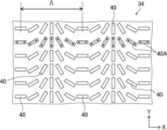
- FIG. 2 is a conceptual diagram for explaining the liquid crystal alignment pattern in the liquid crystal layer of the optical element of the present invention
- 1 is a conceptual diagram of an example of an exposure device that exposes an alignment film
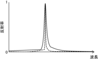
- FIG. 4 is a graph for explaining wavelength-selective reflection of the optical element of the present invention
- It is a figure which shows notionally an example of the conventional optical element.
- optical element and optical sensor of the present invention will be described in detail below based on preferred embodiments shown in the accompanying drawings.
- a numerical range represented by “to” means a range including the numerical values before and after “to” as lower and upper limits.
- (meth)acrylate means “either or both of acrylate and methacrylate”.
- the term “identical” includes the margin of error generally accepted in the technical field.
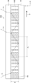
- FIG. 1 conceptually shows an example of the optical element of the present invention.
- the optical element 10 shown in FIG. 1 has a first sheet 12 , a second sheet 14 , and a liquid crystal layer 34 sandwiched between the first sheet and the second sheet 14 .
- the direction of the optical axis 40A derived from the liquid crystal compound 40 is continuous in one direction (X direction). It has a liquid crystal orientation pattern that changes while rotating.
- FIG. 2 is a diagram conceptually showing the liquid crystal alignment pattern in the plane of the liquid crystal layer 34 (in the plane direction of the principal plane).
- the liquid crystal layer 34 has a resonance structure that causes the waveguide mode resonance phenomenon described above.
- the liquid crystal compound 40 is cholesterically aligned along the thickness direction (Z direction).
- the thickness direction of the liquid crystal layer 34 is the lamination direction of the first sheet 12 , the liquid crystal layer 34 and the second sheet 14 .
- FIG. 1 shows the case where the liquid crystal compound 40 in the liquid crystal layer 34 has a helical pitch number of 1 in the cholesteric orientation, but the helical pitch number is not limited to this aspect as will be described later.
- the liquid crystal layer 34 will be detailed later.
- the illustrated optical element 10 has a structure in which the liquid crystal layer 34 is sandwiched between the first sheet 12 and the second sheet 14 .
- the first sheet 12 and the second sheet 14 are sheets having a lower refractive index than the liquid crystal layer 34 . Since the optical element 10 has such a configuration, the incident light L repeats total reflection in the liquid crystal layer 34 and is guided (propagated, propagated, guided).
- the refractive index of the liquid crystal layer 34 is the average refractive index of the liquid crystal compound.
- the first sheet 12 and the second sheet 14 are not limited, and various known sheet-like materials (films, layers, plate-like materials) can be used as long as they have a lower refractive index than the liquid crystal layer 34 . Accordingly, the first sheet 12 and the second sheet 14 may be single-layered or multi-layered.
- the single-layer first sheet 12 and second sheet 14 are made of glass and various resin materials such as triacetyl cellulose (TAC), polyethylene terephthalate (PET), polycarbonate, polyvinyl chloride, acrylic and polyolefin. A sheet is exemplified.
- Examples of the first sheet 12 and the second sheet 14 in the case of being multi-layered include, for example, one of the above-described single-layer sheets as a substrate, and another layer provided on the surface of this substrate. be.
- first sheet 12 and second sheet 14 is a sheet composed of a substrate and a bonding layer, in which the substrate is bonded to the liquid crystal layer 34 via a bonding layer.
- the lamination layer As the lamination layer, as long as it has sufficient light transmittance, it has fluidity when laminating and then becomes solid. It may be a layer made of a pressure-sensitive adhesive that is a soft solid with the shape of ) and does not change its gel-like state after that, or a layer made of a material that has the characteristics of both an adhesive and a pressure-sensitive adhesive.
- the lamination layer is an optically transparent adhesive (OCA (Optical Clear Adhesive)), an optically transparent double-sided tape, and a known adhesive used for laminating sheets in various optical devices, such as an ultraviolet curable resin. Layers may be used.
- OCA optical Clear Adhesive
- Layers may be used.
- the first sheet 12 and the second sheet 14 preferably have a transmittance of 50% or more, more preferably 70% or more, and even more preferably 85% or more to the corresponding light.
- the thickness of the first sheet 12 and the second sheet 14 is not limited, and the application of the optical element 10, the material for forming the first sheet 12 and the second sheet 14, and the layer structure of the first sheet 12 and the second sheet 14 etc., it may be set as appropriate. Also, the first sheet 12 and the second sheet 14 may be the same or different.
- the refractive index of the liquid crystal layer 34 may be higher than that of the medium in contact with the main surface of the liquid crystal layer 34 . Therefore, in the optical element of the present invention, a gas such as an air layer (atmosphere) may be in contact with the main surface of the liquid crystal layer 34 . That is, the optical element of the present invention may have only the liquid crystal layer 34 and one of the first sheet 12 and the second sheet 14, or may be composed only of the liquid crystal layer 34. good.
- the principal surface is the largest surface of the sheet (film, plate, layer), and is usually both sides of the sheet in the thickness direction.
- a liquid crystal layer 34 is provided between the first sheet 12 and the second sheet 14 in the optical element 10 .
- the direction of the optical axis 40A derived from the liquid crystal compound 40 rotates continuously in one direction within the plane. It has a changing liquid crystal alignment pattern.
- the "optical axis derived from the liquid crystal compound” is also referred to as the “optical axis of the liquid crystal compound” or simply the “optical axis”.
- the liquid crystal compounds 40 are arranged along the X direction and the Y direction, which are orthogonal to each other, in the plane direction of the main surface of the liquid crystal layer 34 .
- the Y direction is a direction perpendicular to the plane of the paper.
- the direction of the optical axis 40A of the liquid crystal compound 40 changes while continuously rotating along the X direction, which is one direction in the plane of the liquid crystal layer 34 .
- the liquid crystal compounds 40 having the same optical axis 40A are aligned at regular intervals.
- the liquid crystal compound 40 is cholesterically aligned and stacked in the thickness direction (Z direction) as shown in FIG.
- the thickness direction that is, the Z direction, is the direction perpendicular to the plane of the paper.
- the orientation of the optic axis 40A of the liquid crystal compound 40 changes while continuously rotating in one direction within the plane
- the angle formed by the optic axis 40A and the X direction varies depending on the position in the X direction. It means that along the X direction, the angle between the optical axis 40A and the X direction changes gradually from ⁇ to ⁇ +180° or ⁇ 180°. That is, the plurality of liquid crystal compounds 40 arranged along the X direction change while the optical axis 40A rotates along the X direction by a constant angle as shown in FIG.
- the angle difference between the optical axes 40A adjacent to each other in the X direction is not limited, but is preferably 45° or less, more preferably 15° or less, and still more preferably a smaller angle.
- the optic axis 40A of the liquid crystal compound 40 is intended to be the long molecular axis of the rod-like liquid crystal compound.
- the optical axis 40A of the liquid crystal compound 40 is intended to be an axis parallel to the normal direction to the discotic surface of the discotic liquid crystal compound.
- a rod-like liquid crystal compound is exemplified as the liquid crystal compound 40 .
- the optical axis 40A of the liquid crystal compound 40 rotates 180° in the X direction in which the optical axis 40A rotates continuously within the plane.
- the height (distance) is one period in the liquid crystal alignment pattern. That is, the distance between the centers in the X direction of two liquid crystal compounds 40 having the same angle with respect to the X direction is one period in the liquid crystal alignment pattern.
- the center-to-center distance in the X direction of two liquid crystal compounds 40 whose X direction and the direction of the optical axis 40A match is one period in the liquid crystal alignment pattern.
- the liquid crystal alignment pattern of the liquid crystal layer 34 repeats this one period in one direction in which the direction of the X direction, ie, the optical axis 40A, rotates continuously and changes.
- the liquid crystal layer 34 acts as a liquid crystal diffraction element.
- one period of such a liquid crystal alignment pattern becomes a period ⁇ (one period ⁇ ) of the periodic structure of the diffraction element (diffraction grating).
- the liquid crystal layer 34 has a resonance structure that causes the waveguide mode resonance phenomenon described above. Therefore, the liquid crystal layer 34 acts as a diffraction grating having a sub-wavelength grating whose period ⁇ is shorter than the wavelength of light selectively reflected by the optical element 10 (liquid crystal layer 34). This point will be described in detail later.
- the liquid crystal compound 40 forming the liquid crystal layer 34 has the same optic axis 40A in the Y direction orthogonal to the X direction, that is, the Y direction orthogonal to one direction in which the optic axis 40A rotates continuously.
- the angle between the optic axis 40A of the liquid crystal compound 40 and the X direction is equal in the Y direction.
- the liquid crystal layer 34 having such a liquid crystal alignment pattern can be formed, for example, using an alignment film having an alignment pattern corresponding to the liquid crystal alignment pattern and for orienting the liquid crystal compound 40 in a predetermined liquid crystal alignment pattern.
- the alignment film may be used as either one of the first sheet 12 and the second sheet 14 in the optical element of the present invention.
- Various known alignment films can be used as long as they can align the liquid crystal compound.
- rubbed films made of organic compounds such as polymers, oblique vapor deposition films of inorganic compounds, films with microgrooves, and Langmuir films of organic compounds such as ⁇ -tricosanoic acid, dioctadecylmethylammonium chloride and methyl stearate.
- LB Liquinuir-Blodgett
- the alignment film by rubbing treatment can be formed by rubbing the surface of the polymer layer with paper or cloth several times in one direction.
- Materials used for the alignment film include polyimide, polyvinyl alcohol, polymers having a polymerizable group described in JP-A-9-152509, JP-A-2005-097377, JP-A-2005-099228, and A material used for forming an alignment film or the like described in JP-A-2005-128503 is preferable.
- a so-called photo-alignment film obtained by irradiating a photo-alignment material with polarized or non-polarized light to form an alignment film is preferably used. That is, as the alignment film, a photo-alignment film formed by coating a substrate with a photo-alignment material is preferably used. Irradiation with polarized light can be performed in a direction perpendicular to or oblique to the photo-alignment film, and irradiation with non-polarized light can be performed in a direction oblique to the photo-alignment film.
- photo-alignment materials used in the alignment film include, for example, JP-A-2006-285197, JP-A-2007-076839, JP-A-2007-138138, and JP-A-2007-094071.
- Preferable examples include photodimerizable compounds described in JP-A-177561 and JP-A-2014-12823, particularly cinnamate compounds, chalcone compounds and coumarin compounds.
- azo compounds, photocrosslinkable polyimides, photocrosslinkable polyamides, photocrosslinkable polyesters, cinnamate compounds, and chalcone compounds are preferably used.
- the thickness of the alignment film is not limited, and the thickness that can obtain the required alignment function may be appropriately set according to the material forming the alignment film.
- the method for forming the alignment film is not limited, and various known methods can be used depending on the material for forming the alignment film. As an example, a method of forming an alignment pattern by applying an alignment film to the surface of a base material, drying the alignment film, and then exposing the alignment film to laser light is exemplified.
- FIG. 3 conceptually shows an example of an exposure apparatus that exposes an alignment film to form an alignment pattern.
- the exposure device 60 shown in FIG. 3 includes a light source 64 having a laser 62, a ⁇ /2 plate 65 for changing the polarization direction of the laser beam M emitted by the laser 62, and a beam MA and a beam MA of the laser beam M emitted by the laser 62. It comprises a polarizing beam splitter 68 that splits the MB into two, mirrors 70A and 70B placed respectively on the optical paths of the two split beams MA and MB, and ⁇ /4 plates 72A and 72B.
- the light source 64 emits linearly polarized light P 0 .
- the ⁇ /4 plate 72A converts the linearly polarized light P 0 (light ray MA) into right circularly polarized light PR
- the ⁇ /4 plate 72B converts the linearly polarized light P 0 (light ray MB) into left circularly polarized light P L .
- the alignment film 32 before the alignment pattern is formed is placed at the exposure position, and the two light beams MA and MB are crossed and interfered on the alignment film, and the interference light is irradiated to the alignment film 32 for exposure. . Due to the interference at this time, the polarization state of the light with which the alignment film is irradiated periodically changes in the form of interference fringes. As a result, an alignment film having an alignment pattern in which the alignment state changes periodically is obtained. In the following description, an alignment film having this alignment pattern is also referred to as a "patterned alignment film". In the exposure device 60, the period of the alignment pattern can be adjusted by changing the crossing angle ⁇ of the two light beams MA and MB.
- the length of one cycle in which the optical axis 40A rotates 180° can be adjusted.
- the liquid crystal layer 34 By forming the liquid crystal layer 34 on the alignment film having such an alignment pattern in which the alignment state changes periodically, the optical axis 40A of the liquid crystal compound 40 is continuously aligned along one direction, as described later.
- a liquid crystal layer 34 can be formed having a rotating liquid crystal alignment pattern. Further, by rotating the optical axes of the ⁇ /4 plates 72A and 72B by 90°, the direction of rotation of the optical axis 40A can be reversed.
- the patterned alignment film is a liquid crystal in which the orientation of the optic axis of the liquid crystal compound in the liquid crystal layer formed on the patterned alignment film changes while continuously rotating along at least one in-plane direction. It has an orientation pattern for orienting the liquid crystal compound so as to form an orientation pattern. Assuming that the orientation axis of the patterned orientation film is along the direction in which the liquid crystal compound is oriented, the direction of the orientation axis of the patterned orientation film changes while continuously rotating along at least one in-plane direction. It can be said that it has an orientation pattern.
- the orientation axis of the patterned orientation film can be detected by measuring the absorption anisotropy.
- a patterned alignment film is irradiated with linearly polarized light while being rotated and the amount of light transmitted through the patterned alignment film is measured, the direction in which the light amount becomes maximum or minimum gradually changes along one direction in the plane. Observed to change.
- the liquid crystal layer 34 is a liquid crystal in which the direction of the optical axis 40A derived from the liquid crystal compound 40 changes while continuously rotating in the X direction. It has an orientation pattern.
- the liquid crystal layer 34 has a resonance structure that causes the waveguide mode resonance phenomenon (light guide resonance) described above.
- the liquid crystal layer 34 has a structure that allows resonance of light in a specific wavelength band. Therefore, the liquid crystal layer 34 acts as a diffraction grating having a sub-wavelength grating with a sub-wavelength structure whose period ⁇ is shorter than the wavelength of the light to be selectively reflected.
- the liquid crystal compound 40 in the liquid crystal layer 34, is cholesterically aligned along the thickness direction, ie, the Z direction.
- the liquid crystal layer 34 has a structure in which the liquid crystal compounds 40 are spirally swirled and stacked in the thickness direction.
- the optical element 10 of the present invention has such a liquid crystal layer 34, thereby selectively reflecting light in a specific wavelength band by causing a waveguide mode resonance phenomenon using a liquid crystal diffraction element. , the reflection wavelength band can be narrowed.
- FIG. 5 is a diagram conceptually showing a liquid crystal diffraction element that causes a waveguide mode resonance phenomenon, described in Non-Patent Document 1.
- the optical element 100 shown in FIG. 5 has the same configuration as the optical element 10 of the present invention except that the liquid crystal compound 40 in the liquid crystal layer 102 is not cholesterically aligned in the thickness direction (Z direction). Accordingly, in the liquid crystal layer 102 as well, the liquid crystal compound 40 has a liquid crystal alignment pattern in which the optical axis 40A rotates continuously in the X direction.
- One period of the liquid crystal orientation pattern that is, the period ⁇ of the periodic structure of the liquid crystal diffraction element, is the length of the 180° rotation of the optical axis 40A in the X direction. also acts as a diffraction grating with a sub-wavelength grating with a short period ⁇ .
- the waveguide mode resonance phenomenon described below basically applies to the optical element 10 (liquid crystal layer 34) of the present invention in which the liquid crystal compound 40 is cholesterically aligned in the thickness direction. That is, in the following description, if the optical element 100 is replaced with the optical element 10 and the liquid crystal layer 102 is replaced with the liquid crystal layer 34, the optical element 10 of the present invention will be described.
- the light in a specific wavelength band among the guided light is guided in a waveguide mode in which the guided light resonates with the period ⁇ of the liquid crystal layer 102, which is a sub-wavelength grating. A resonance phenomenon is produced.
- the light in this specific wavelength band is emitted from the liquid crystal layer 102 while being guided, and is emitted from the optical element 100 as strong reflected light Lr.
- the angle of diffraction in the diffraction element varies depending on the wavelength of light. Therefore, light in a specific wavelength band is diffracted by the liquid crystal layer 102, and the relationship between the thickness d of the liquid crystal layer 102 and the period ⁇ of the liquid crystal layer 102, which is a sub-wavelength grating, depends on the angle of diffraction. , the waveguide of the light and the period ⁇ resonate. Due to this resonance, the light in the specific wavelength band is amplified while guided, and emitted from the liquid crystal layer 102, that is, the optical element 100, as a strong reflected light Lr.
- the optical element 100 when white light is incident as the light L, as an example, light in a partial wavelength band of red light, light in a partial wavelength band of green light, or partial wavelength of blue light Light in the band is emitted from the optical element 100 as strong reflected light Lr.
- the liquid crystal layer 102 has a resonance structure according to the relationship between the wavelength of light, the thickness d of the liquid crystal layer, and the period ⁇ of the liquid crystal layer 102, which is a sub-wavelength grating.
- the liquid crystal layer 102 has a gap between the guided light and the period ⁇ of the sub-wavelength grating, depending on the relationship between the wavelength of the light and the thickness d of the liquid crystal layer and the period ⁇ of the liquid crystal layer 102 . It has a structure that causes resonance (guided mode resonance phenomenon).
- the emission of the reflected light Lr is like specular reflection, except that the light L is incident and emitted at different positions. That is, if the incident angle of the light L is + ⁇ °, the emission angle of the reflected light Lr is ⁇ °. Light outside the specific wavelength band emitted as the reflected light Lr is not guided in the liquid crystal layer 102, or while being guided in the liquid crystal layer 102, the optical element 100 (liquid crystal layer 102), the reflected light Lr exits to the opposite side.
- the liquid crystal compound 40 is cholesterically aligned in the thickness direction of the liquid crystal layer 34 having a resonance structure that causes a waveguide mode resonance phenomenon. That is, the liquid crystal layer 34 is a layer in which the cholesteric liquid crystal phase is fixed.
- the liquid crystal layer 34 has a resonance structure, and the waveguide mode resonance phenomenon is generated using the liquid crystal diffraction element. , the selective reflection wavelength band can be narrowed.
- Non-Patent Document 1 In a conventional optical element in which the liquid crystal compound 40 is not cholesterically aligned in the thickness direction, as shown in Non-Patent Document 1, that is, FIG. wide.
- the reflectance is normalized with a maximum value of 1. As shown in FIG.
- the reflection wavelength selectivity can be changed by providing a periodic structure of cholesteric orientation of the liquid crystal compound of the liquid crystal layer 34, that is, the liquid crystal diffraction element, in the thickness direction. That is, the inventors have found that the wavelength selectivity of reflection can be changed by cholesterically aligning the liquid crystal compound 40 in the thickness direction to provide a cholesteric structure. Specifically, in the liquid crystal layer 34 having a resonance structure, by cholesterically aligning the liquid crystal compound 40 in the thickness direction, the wavelength band of light that is selectively reflected, that is, the full width at half maximum, as indicated by the dashed line in FIG. can be narrowed.
- the present invention was made by obtaining this knowledge, and an optical element that selectively reflects light in a specific wavelength band by causing a waveguide mode resonance phenomenon using a liquid crystal diffraction element, that is, In an optical element including a liquid crystal layer having a resonance structure, the selective reflection wavelength band can be narrowed by cholesterically orienting the liquid crystal compound of the liquid crystal layer along the thickness direction.
- the liquid crystal layer is a cholesteric liquid crystal layer having a fixed cholesteric liquid crystal phase.
- the cholesteric liquid crystal phase has a helical structure in which the liquid crystal compound 40 is twisted and stacked in the thickness direction, and the liquid crystal compound 40 is helically stacked by one rotation (360° rotation). is one helical pitch (pitch P), and the liquid crystal compounds 40 that are helically swirled have a structure in which a plurality of pitches are laminated.
- the number of helical pitches is preferably 3 to 8.
- the number of helical pitches means the number of helical pitches (number of turns) of the helical structure derived from the cholesteric liquid crystal phase in the liquid crystal layer.
- the cholesteric liquid crystal phase specifically means that the twist angle of the liquid crystal compound 40 in the liquid crystal layer is 360° or more.
- a cholesteric liquid crystal phase exhibits selective reflectivity for either left-handed circularly polarized light or right-handed circularly polarized light at a particular wavelength, depending on the pitch P and the twist direction of the helix by the liquid crystal compound 40. . Specifically, the longer the pitch P of the spiral, the more selectively the longer wavelength light is reflected. Further, when the twist direction of the helix by the liquid crystal compound 40 is right, it selectively reflects right-handed circularly polarized light, and when it is left-handed, it selectively reflects left-handed circularly polarized light. In addition, the cholesteric liquid crystal phase transmits light other than light to be selectively reflected.
- the helical pitch number of the liquid crystal compound 40 in the liquid crystal layer 34 can be adjusted by the type and amount of chiral agent added to the liquid crystal composition, which will be described later.
- the twist direction of the cholesteric alignment of the liquid crystal compound 40 in the liquid crystal layer 34 can be selected depending on the type of liquid crystal compound and/or chiral agent added to the liquid crystal composition described later.
- the twist direction (spiral turning direction) of the cholesteric alignment of the liquid crystal compound 40 in the liquid crystal layer 34 is not limited, and may be right twist or left twist.
- the light incident on the liquid crystal layer 34 may be right-handed circularly polarized light, left-handed circularly polarized light, elliptically polarized light, linearly polarized light, or non-polarized light.
- the effects of the invention can be obtained.
- right-handed circularly polarized light is used as the light incident on the liquid crystal layer 34.
- left-handed circularly polarized light is used as the light incident on the liquid crystal layer
- the use of polarized light is preferable because the waveguide mode resonance becomes stronger and a strong signal can be easily obtained.
- a polarizing plate or wave plate may be arranged to give preferable polarized light to the incident side.
- a polarizing plate or wave plate may also be arranged on the output side. In this way, a light guide mode with a high SN ratio can be detected.
- the orientation of the cholesteric twist axis may be parallel to the normal direction of the liquid crystal layer 34, or may be inclined.
- the axis of the cholesteric twist is the pretilt angle of the liquid crystal compound on one surface side and the other surface side of the liquid crystal layer 34, and the oblique period generated by the combination of the period due to the spontaneous twisting force of the cholesteric liquid crystal itself and the in-plane orientation period.
- the orientation of the cholesteric torsion axis may vary rather than be constant in the thickness direction.
- the period ⁇ of the liquid crystal layer 34 is not limited, but should be smaller than the wavelength of the selectively reflected light. More specifically, the period .LAMBDA. A value large enough to generate diffracted waves, and the period ⁇ capable of forming a resonance structure that causes a waveguide mode resonance phenomenon is appropriately set according to the wavelength band of light to be selectively reflected, the thickness of the liquid crystal layer 34, and the like. do it.
- the period ⁇ of the liquid crystal layer 34 is preferably 0.1 to 100 ⁇ m, more preferably 0.1 to 10 ⁇ m.
- the thickness d of the liquid crystal layer 34 is not limited, and the thickness can form a resonance structure that causes a waveguide mode resonance phenomenon according to the wavelength band of light to be selectively reflected, the period ⁇ of the liquid crystal layer 34, and the like. d may be set as appropriate.
- the thickness of the liquid crystal layer 34 is preferably 0.1-100 ⁇ m, more preferably 0.1-10 ⁇ m.
- the first sheet 12 and the second sheet 14 sandwiching the liquid crystal layer 34 have a lower refractive index than the liquid crystal layer.
- the refractive index of the first sheet 12 and the second sheet 14 should be lower than that of the liquid crystal layer 34 .
- the difference in refractive index between the two is not limited, but is preferably 0.05 to 1, more preferably 0.05 to 0.7.
- Such a liquid crystal layer 34 can be formed by fixing a liquid crystal phase in which a liquid crystal compound is aligned in a predetermined alignment state in a layer.
- the structure in which the liquid crystal phase is fixed may be any structure as long as the orientation of the liquid crystal compound in the liquid crystal phase is maintained.
- a polymerizable liquid crystal compound is oriented in a predetermined liquid crystal phase, polymerized and cured by ultraviolet irradiation, heating, or the like to form a layer without fluidity, and at the same time, by an external field or external force.
- a structure that is changed to a state that does not cause a change in orientation is preferred.
- the liquid crystal compound 40 does not have to exhibit liquid crystallinity in the liquid crystal layer.
- the polymerizable liquid crystal compound may be polymerized by a curing reaction and lose liquid crystallinity.
- An example of a material used to form the liquid crystal layer 34 is a liquid crystal composition containing a liquid crystal compound.
- the liquid crystal compound is preferably a polymerizable liquid crystal compound.
- the liquid crystal composition used for forming the liquid crystal layer 34 may further contain a surfactant and a chiral agent.
- the polymerizable liquid crystal compound may be a rod-like liquid crystal compound or a discotic liquid crystal compound.
- rod-like polymerizable liquid crystal compounds include rod-like nematic liquid crystal compounds.
- Rod-shaped nematic liquid crystal compounds include azomethines, azoxys, cyanobiphenyls, cyanophenyl esters, benzoic acid esters, cyclohexanecarboxylic acid phenyl esters, cyanophenylcyclohexanes, cyano-substituted phenylpyrimidines, and alkoxy-substituted phenylpyrimidines.
- phenyldioxane, tolan, and alkenylcyclohexylbenzonitriles are preferably used. Not only low-molecular-weight liquid crystal compounds but also high-molecular liquid-crystal compounds can be used.
- a polymerizable liquid crystal compound is obtained by introducing a polymerizable group into a liquid crystal compound.
- polymerizable groups include unsaturated polymerizable groups, epoxy groups, and aziridinyl groups, with unsaturated polymerizable groups being preferred, and ethylenically unsaturated polymerizable groups being more preferred.
- Polymerizable groups can be introduced into molecules of liquid crystal compounds by various methods.
- the number of polymerizable groups possessed by the polymerizable liquid crystal compound is preferably 1 to 6, more preferably 1 to 3. Examples of polymerizable liquid crystal compounds are described in Makromol. Chem. , 190, 2255 (1989), Advanced Materials 5, 107 (1993), U.S. Pat. No. 4,683,327, U.S.
- a polymerizable liquid crystal compound such as a cyclic organopolysiloxane compound disclosed in JP-A-57-165480 can be used.
- a polymer liquid crystal compound described above a polymer having a mesogenic group exhibiting liquid crystal introduced into the main chain, the side chain, or both of the main chain and the side chain, and a polymer cholesteric compound having a cholesteryl group introduced into the side chain.
- Liquid crystals, liquid crystalline polymers as disclosed in JP-A-9-133810, and liquid-crystalline polymers as disclosed in JP-A-11-293252 and the like can be used.
- discotic Liquid Crystal Compound As the discotic liquid crystal compound, for example, those described in JP-A-2007-108732 and JP-A-2010-244038 can be preferably used.
- the amount of the polymerizable liquid crystal compound added in the liquid crystal composition is preferably 75 to 99.9% by mass, and preferably 80 to 99%, based on the solid content mass (mass excluding the solvent) of the liquid crystal composition. % by mass is more preferred, and 85 to 90% by mass is even more preferred.
- the liquid crystal composition used for forming the liquid crystal layer may contain a surfactant.
- the surfactant is preferably a compound that can stably or quickly function as an alignment control agent that contributes to the alignment of the liquid crystal compound 40 in the liquid crystal layer 34 .
- Examples of surfactants include silicone-based surfactants and fluorine-based surfactants, with fluorine-based surfactants being preferred examples.
- the surfactant include compounds described in paragraphs [0082] to [0090] of JP-A-2014-119605, and compounds described in paragraphs [0031] to [0034] of JP-A-2012-203237. , Compounds exemplified in paragraphs [0092] and [0093] of JP-A-2005-099248, paragraphs [0076] to [0078] and paragraphs [0082] to [0085] of JP-A-2002-129162 compounds exemplified therein, and fluorine (meth)acrylate polymers described in paragraphs [0018] to [0043] of JP-A-2007-272185.
- surfactant may be used individually by 1 type, and may use 2 or more types together.
- fluorosurfactant compounds described in paragraphs [0082] to [0090] of JP-A-2014-119605 are preferable.
- the amount of the surfactant added in the liquid crystal composition is preferably 0.01 to 10% by mass, more preferably 0.01 to 5% by mass, and 0.02 to 1% by mass with respect to the total mass of the liquid crystal compound. is more preferred.
- a chiral agent has a function of inducing cholesteric alignment in the thickness direction of the liquid crystal compound 40 .
- the chiral agent may be selected depending on the purpose, since the twist direction or twist angle induced by the compound differs.
- the chiral agent is not particularly limited, and known compounds (for example, liquid crystal device handbook, Chapter 3, Section 4-3, chiral agent for TN (twisted nematic), STN (Super Twisted Nematic), page 199, Japan Society for the Promotion of Science 142nd Committee, 1989), isosorbide, isomannide derivatives and the like can be used.
- Chiral agents generally contain an asymmetric carbon atom, but axially chiral compounds or planar chiral compounds that do not contain an asymmetric carbon atom can also be used as chiral agents.
- Examples of axially or planarly chiral compounds include binaphthyl, helicene, paracyclophane, and derivatives thereof.
- the chiral agent may have a polymerizable group. When both the chiral agent and the liquid crystal compound have a polymerizable group, a repeating unit derived from the polymerizable liquid crystal compound and a repeating unit derived from the chiral agent are formed by the polymerization reaction of the polymerizable chiral agent and the polymerizable liquid crystal compound.
- the polymerizable group possessed by the polymerizable chiral agent is preferably the same type of group as the polymerizable group possessed by the polymerizable liquid crystal compound. Therefore, the polymerizable group of the chiral agent is also preferably an unsaturated polymerizable group, an epoxy group or an aziridinyl group, more preferably an unsaturated polymerizable group, and an ethylenically unsaturated polymerizable group. More preferred. Also, the chiral agent may be a liquid crystal compound.
- the chiral agent has a photoisomerizable group
- the photoisomerizable group is preferably an isomerization site of a compound exhibiting photochromic properties, an azo group, an azoxy group, or a cinnamoyl group.
- Specific compounds include JP-A-2002-080478, JP-A-2002-080851, JP-A-2002-179668, JP-A-2002-179669, JP-A-2002-179670, JP-A-2002- 179681, JP-A-2002-179682, JP-A-2002-338575, JP-A-2002-338668, JP-A-2003-313189, and compounds described in JP-A-2003-313292, etc. can be used.
- the twist angle of the liquid crystal compound 40 along the thickness direction of the liquid crystal layer 34 can be adjusted by the amount of chiral agent. Therefore, the content of the chiral agent in the liquid crystal composition may be appropriately set according to the target twist angle of the liquid crystal compound 40 along the thickness direction.
- the liquid crystal composition preferably contains a polymerization initiator.
- the polymerization initiator used is preferably a photopolymerization initiator capable of initiating the polymerization reaction by ultraviolet irradiation.
- photoinitiators include ⁇ -carbonyl compounds (described in US Pat. Nos. 2,367,661 and 2,367,670), acyloin ethers (described in US Pat. No. 2,448,828), ⁇ -hydrocarbons substituted aromatic acyloin compounds (described in US Pat. No.
- the content of the photopolymerization initiator in the liquid crystal composition is preferably 0.1 to 20% by mass, more preferably 0.5 to 12% by mass, based on the total mass of the liquid crystal compound.
- the liquid crystal composition may optionally contain a cross-linking agent in order to improve film strength and durability after curing.
- a cross-linking agent one that is cured by ultraviolet rays, heat, humidity, and the like can be preferably used.
- the cross-linking agent is not particularly limited and can be appropriately selected depending on the intended purpose.
- polyfunctional acrylate compounds such as trimethylolpropane tri(meth)acrylate and pentaerythritol tri(meth)acrylate
- epoxy compounds such as ethylene glycol diglycidyl ether
- aziridine compounds such as 2,2-bishydroxymethylbutanol-tris[3-(1-aziridinyl)propionate] and 4,4-bis(ethyleneiminocarbonylamino)diphenylmethane
- hexa Isocyanate compounds such as methylene diisocyanate and biuret isocyanate
- alkoxysilane compounds such as vinyltrimethoxysilane and N-(2-aminoethyl)3-aminopropyltrimethoxysilane.
- the content of the cross-linking agent is preferably 3 to 20% by mass, more preferably 5 to 15% by mass, based on the solid mass of the liquid crystal composition. When the content of the cross-linking agent is within the above range, the effect of improving the cross-linking density is likely to be obtained, and the stability of the liquid crystal phase is further improved.
- the liquid crystal composition may further contain polymerization inhibitors, antioxidants, ultraviolet absorbers, light stabilizers, colorants, metal oxide fine particles, etc., within a range that does not reduce the optical performance. can be added at
- the liquid crystal composition is preferably used as a liquid when forming the liquid crystal layer 34 .
- the liquid crystal composition may contain a solvent.
- the solvent is not limited and can be appropriately selected according to the purpose, but organic solvents are preferred.
- the organic solvent is not limited and can be appropriately selected depending on the purpose. Examples include ketones, alkyl halides, amides, sulfoxides, heterocyclic compounds, hydrocarbons, esters, and ethers. etc. These may be used individually by 1 type, and may use 2 or more types together. Among these, ketones are preferred in consideration of the load on the environment.
- a liquid crystal composition is applied to the surface on which the liquid crystal layer 34 is to be formed, and after the liquid crystal compound 40 is aligned in a desired liquid crystal phase state, the liquid crystal composition is cured to form the liquid crystal layer.
- 34 is preferred. That is, when the liquid crystal layer 34 is formed on the alignment film described above, the liquid crystal composition is applied to the alignment film, the liquid crystal compound is cholesterically aligned, and then the liquid crystal compound is cured to form the liquid crystal layer 34 . is preferred.
- the liquid crystal composition can be applied by printing methods such as inkjet and scroll printing, and known methods such as spin coating, bar coating and spray coating, which can uniformly apply the liquid to the sheet.
- the applied liquid crystal composition is dried and/or heated as necessary, and then cured to form a liquid crystal layer.
- the liquid crystal compound 40 in the liquid crystal composition may be cholesterically aligned in this drying and/or heating step.
- the heating temperature is preferably 200° C. or lower, more preferably 130° C. or lower.
- the aligned liquid crystal compound is further polymerized as necessary.
- Polymerization may be either thermal polymerization or photopolymerization by light irradiation, but photopolymerization is preferred.
- the irradiation energy is preferably 20 mJ/cm 2 to 50 J/cm 2 , more preferably 50 to 1500 mJ/cm 2 .
- light irradiation may be performed under heating conditions or under a nitrogen atmosphere.
- the wavelength of the ultraviolet rays to be irradiated is preferably 250 to 430 nm.
- the optical sensor of the present invention is an optical sensor using the optical element of the present invention described above.
- the selective reflection wavelength band of the optical element of the present invention is sensitive to refractive index changes around the liquid crystal diffractive element or liquid crystal layer. Therefore, the optical sensor of the present invention can be suitably used as a refractive index sensor.
- an object whose refractive index is to be measured is placed on the liquid crystal layer included in the optical element of the present invention.
- the position of the peak wavelength of the reflected light from the optical sensor of the present invention shifts depending on the refractive index of the object to be measured.
- the relationship between the refractive index of the substance placed on the liquid crystal layer and the position of the peak wavelength of the reflected light is grasped in advance, and an object to be measured whose refractive index is unknown is placed on the liquid crystal layer, and the reflected light
- the refractive index of the object to be measured can be obtained.
- the closer the average refractive index of the liquid crystal layer and the refractive index of the object to be measured the greater the shift width of the peak wavelength of the reflected light. It is possible to obtain the refractive index of the object to be measured.
- the refractive index of the object to be measured can be obtained more accurately.
- the average refractive index of the liquid crystal layer is the average value of the refractive index in the in-plane direction of the liquid crystal layer in which the refractive index is the highest and the refractive index in the direction perpendicular to the direction in which the refractive index is highest. Further, when a substance having a predetermined refractive index is arranged on the liquid crystal layer and the incident angle of incident light is changed, the reflected light is detected at a specific incident angle.
- the angle at which the reflected light from the optical sensor of the present invention peaks shifts depending on the refractive index of the object to be measured.
- the relationship between the refractive index of the substance placed on the liquid crystal layer and the incident angle at which the reflected light is detected is grasped in advance, and the object to be measured whose refractive index is unknown is placed on the liquid crystal layer. Then, by measuring the incident angle at which the reflected light is obtained, the refractive index of the object to be measured can be obtained.
- the optical sensor of the present invention can be suitably used for biochemical sensors and the like.
- the optical element of the present invention can be suitably used for wavelength selection filters, polarization separation elements, retardation plates, optical switches, etc., in addition to optical sensors.
- Alignment film forming coating solution ⁇ ⁇
- the following optical alignment material 1.00 parts by mass ⁇ Water 16.00 parts by mass ⁇ Butoxyethanol 42.00 parts by mass ⁇ Propylene glycol monomethyl ether 42.00 parts by mass ⁇ ⁇
- the alignment film P-2 thus obtained was irradiated with polarized ultraviolet rays (50 mJ/cm 2 , using an ultra-high pressure mercury lamp) to expose the alignment film P-2.
- the alignment film was exposed using the exposure apparatus shown in FIG. 3 to form an alignment film P-2 having an alignment pattern.
- a laser that emits laser light with a wavelength (325 nm) was used.
- the amount of exposure by interference light was set to 300 mJ/cm 2 .
- the crossing angle (crossing angle ⁇ ) of the two lights is such that one period ⁇ (the length in which the optical axis rotates 180°) of the alignment pattern formed by the interference of the two laser lights is 0.4 ⁇ m. was adjusted.
- composition B-1 As a liquid crystal composition for forming a liquid crystal layer, the following composition B-1 was prepared.
- Rod-shaped liquid crystal compound L-1 100.00 parts by mass ⁇
- Polymerization initiator manufactured by BASF, Irgacure (registered trademark) 907
- 3.00 parts by mass Photosensitizer manufactured by Nippon Kayaku, KAYACURE DETX-S
- 1.00 parts by mass Leveling agent T-1 0.08 parts by mass Methyl ethyl ketone 2000.00 parts by mass ⁇ ⁇
- Rod-shaped liquid crystal compound L-1 (including the following structure in the mass ratio shown on the right)
- the liquid crystal layer was formed by coating the composition B-1 on the alignment film P-2 in multiple layers. First, the composition B-1 for the first layer was applied on the alignment film, heated, cooled, and then cured with ultraviolet light to prepare a liquid crystal fixing layer. Then, the coating was applied, followed by heating, cooling, and UV curing.
- the following composition B-1 was applied on the alignment film P-2, the coating film was heated on a hot plate to 80 ° C., and then at 80 ° C., The orientation of the liquid crystal compound was fixed by irradiating the coating film with ultraviolet rays having a wavelength of 365 nm at an irradiation amount of 300 mJ/cm 2 using a high-pressure mercury lamp in a nitrogen atmosphere.
- the second and subsequent layers were overcoated on this liquid crystal fixing layer, heated under the same conditions as above, cooled, and then UV-cured to produce a liquid crystal fixing layer.
- the liquid crystal layer was formed by repeating coating until the total thickness reached a desired thickness.
- the refractive index difference ⁇ n of the cured layer of the liquid crystal composition B-1 was determined by coating the liquid crystal composition B-1 on a separately prepared support with an alignment film for retardation measurement, and using the director of the liquid crystal compound as the base material.
- the retardation Re( ⁇ ) and film thickness of the liquid crystal fixed layer obtained by horizontally aligning the liquid crystal layer and fixing it by ultraviolet irradiation were measured and obtained.
- ⁇ n ⁇ can be calculated by dividing the retardation Re( ⁇ ) by the film thickness.
- Retardation Re( ⁇ ) was measured at a target wavelength using Axoscan manufactured by Axometrix, and film thickness was measured using SEM.
- the refractive index ne( ⁇ ) for extraordinary light and the refractive index no( ⁇ ) for ordinary light were measured with an Abbe refractometer.
- the refractive index anisotropy ⁇ n( ⁇ ) was obtained from the difference between ne( ⁇ ) and no( ⁇ ).
- ⁇ is the wavelength of incident light. In the following, the wavelength ⁇ of incident light is assumed to be 633 nm.
- the twist angle in the thickness direction of the liquid crystal layer was 0°. Also, in the cross-sectional image obtained by SEM, bright and dark lines were observed perpendicular to the lower interface of the liquid crystal layer (the interface with the glass substrate). These bright and dark lines are observed due to the structure in which the liquid crystal compounds oriented in the same direction are stacked in the thickness direction.
- the wavelength dependence of the reflectance of the manufactured optical element was measured.
- a laser beam was incident from the support side of the optical element in the direction normal to the main surface of the optical element, and the reflected light was measured.
- the light source, spectrometer, and detector used were Coherent Libra, HORIBA Jobin-Yvon iHR-320, and Andor Newton-EM, respectively.
- the measurement wavelength was in the range of 580-680 nm.
- Right-handed circularly polarized light was incident on the liquid crystal layer.
- a sharp reflected light peak was observed, indicating a waveguide mode resonance phenomenon.
- the peak wavelength was 607 nm.
- the reflection wavelength bandwidth was 0.5 nm.
- Example 1 An optical element was produced in the same manner as in Comparative Example 1, except that in forming the liquid crystal layer of Comparative Example 1, the composition B-1 was changed to the following composition B-2.
- Composition B-2 ⁇ ⁇
- Rod-shaped liquid crystal compound L-1 100.00 parts by mass ⁇
- Right-handed chiral agent Ch-A 3.42 parts by mass ⁇
- Polymerization initiator manufactured by BASF, Irgacure (registered trademark) 907) 3.00 parts by mass Photosensitizer (manufactured by Nippon Kayaku, KAYACURE DETX-S) 1.00 parts by mass Leveling agent T-1 0.08 parts by mass Methyl ethyl ketone 2000.00 parts by mass ⁇ ⁇
- Example 2 An optical element was produced in the same manner as in Example 1, except that the chiral agent Ch-A in composition B-2 was changed to 5.70 parts by mass in the formation of the liquid crystal layer of Example 1.
- Example 2 functions as an optical element having a narrower reflection wavelength bandwidth than Comparative Example.
- Example 3 An optical element was produced in the same manner as in Example 1, except that the amount of the chiral agent Ch-A in composition B-2 was changed to 9.13 parts by mass in the formation of the liquid crystal layer of Example 1.
- Example 3 functions as an optical element having a narrower reflection wavelength bandwidth than Comparative Example.
- Example 11 In the preparation of the optical element of Example 2, the standard refractive liquid was changed from Cargille Lab's Certified Reflective index liquids (refractive index: 1.510) to Cargille Lab's Certified Reflective index liquids (refractive index: 1.490). An optical element was produced in the same manner as in Example 2.
- Example 11 shows that a minute change in the refractive index in the vicinity of the liquid crystal layer can be preferably detected from the wavelength of the reflection wavelength peak.
- Example 12 In the preparation of the optical element of Example 2, the standard refractive liquid was changed from Cargille Lab's Certified Reflective index liquids (refractive index: 1.510) to Cargille Lab's Certified Reflective index liquids (refractive index: 1.500). An optical element was produced in the same manner as in Example 2.
- Example 12 shows that a minute change in the refractive index in the vicinity of the liquid crystal layer can be preferably detected from the wavelength of the reflection wavelength peak.
- Example 13 In the preparation of the optical element of Example 2, the standard refractive liquid was changed from Cargille Lab's Certified Reflective index liquids (refractive index: 1.510) to Cargille Lab's Certified Reflective index liquids (refractive index: 1.520). An optical element was produced in the same manner as in Example 2.
- Example 13 shows that a minute change in refractive index in the vicinity of the liquid crystal layer can be preferably detected from the wavelength of the reflection wavelength peak.
- the refractive index of the liquid crystal layer used in these examples is 1.61855, which is the average of the values ne(633) of 1.6944 and no(633) of 1.5427.
- the difference in reflection peak wavelength between Examples 11 and 12 is 0.4 nm
- the difference between Examples 12 and 2 is 0.5 nm
- the difference between Examples 2 and 13 is 0.4 nm. was 0.8 nm. From this, the closer the refractive index of the liquid crystal layer and the refractive index near the liquid crystal layer (the refractive index of the layer of the standard refractive liquid) are, the greater the change in the reflection peak with respect to the change in the refractive index near the liquid crystal layer. can be detected with high sensitivity.
- wavelength selection filters optical sensors, etc.
- Reference Signs List 10 100 optical element 12 first sheet 14 second sheet 30 substrate 32 alignment film 34 liquid crystal layer 40 liquid crystal compound 40A optical axis 60 exposure device 62 laser 64 light source 65 ⁇ /2 plate 68 polarizing beam splitter 70A, 70B mirror 72A, 72B ⁇ /4 plate M laser light MA, MB light beam P O linearly polarized light
Landscapes
- Physics & Mathematics (AREA)
- General Physics & Mathematics (AREA)
- Optics & Photonics (AREA)
- Chemical & Material Sciences (AREA)
- General Health & Medical Sciences (AREA)
- Biochemistry (AREA)
- Analytical Chemistry (AREA)
- Life Sciences & Earth Sciences (AREA)
- Immunology (AREA)
- Pathology (AREA)
- Health & Medical Sciences (AREA)
- Crystallography & Structural Chemistry (AREA)
- Nonlinear Science (AREA)
- Liquid Crystal (AREA)
- Polarising Elements (AREA)
Priority Applications (2)
| Application Number | Priority Date | Filing Date | Title |
|---|---|---|---|
| JP2023565040A JPWO2023100916A1 (https=) | 2021-11-30 | 2022-11-30 | |
| US18/677,581 US20240319420A1 (en) | 2021-11-30 | 2024-05-29 | Optical element and optical sensor |
Applications Claiming Priority (2)
| Application Number | Priority Date | Filing Date | Title |
|---|---|---|---|
| JP2021194687 | 2021-11-30 | ||
| JP2021-194687 | 2021-11-30 |
Related Child Applications (1)
| Application Number | Title | Priority Date | Filing Date |
|---|---|---|---|
| US18/677,581 Continuation US20240319420A1 (en) | 2021-11-30 | 2024-05-29 | Optical element and optical sensor |
Publications (1)
| Publication Number | Publication Date |
|---|---|
| WO2023100916A1 true WO2023100916A1 (ja) | 2023-06-08 |
Family
ID=86612231
Family Applications (1)
| Application Number | Title | Priority Date | Filing Date |
|---|---|---|---|
| PCT/JP2022/044088 Ceased WO2023100916A1 (ja) | 2021-11-30 | 2022-11-30 | 光学素子および光学センサー |
Country Status (3)
| Country | Link |
|---|---|
| US (1) | US20240319420A1 (https=) |
| JP (1) | JPWO2023100916A1 (https=) |
| WO (1) | WO2023100916A1 (https=) |
Cited By (1)
| Publication number | Priority date | Publication date | Assignee | Title |
|---|---|---|---|---|
| WO2025070729A1 (ja) * | 2023-09-29 | 2025-04-03 | 富士フイルム株式会社 | 光学デバイスおよびヘッドマウントディスプレイ |
Families Citing this family (1)
| Publication number | Priority date | Publication date | Assignee | Title |
|---|---|---|---|---|
| WO2022239858A1 (ja) * | 2021-05-14 | 2022-11-17 | 富士フイルム株式会社 | 光学素子および光学センサー |
Citations (3)
| Publication number | Priority date | Publication date | Assignee | Title |
|---|---|---|---|---|
| JP2019536101A (ja) * | 2016-11-18 | 2019-12-12 | マジック リープ, インコーポレイテッドMagic Leap,Inc. | 広入射角範囲の光を再指向するための多層液晶回折格子 |
| WO2020122128A1 (ja) * | 2018-12-11 | 2020-06-18 | 富士フイルム株式会社 | 導光素子、画像表示装置およびセンシング装置 |
| WO2020122127A1 (ja) * | 2018-12-11 | 2020-06-18 | 富士フイルム株式会社 | コレステリック液晶層およびコレステリック液晶層の形成方法、ならびに、積層体、導光素子および画像表示装置 |
Family Cites Families (4)
| Publication number | Priority date | Publication date | Assignee | Title |
|---|---|---|---|---|
| JP6975258B2 (ja) * | 2017-12-27 | 2021-12-01 | 富士フイルム株式会社 | 光学素子およびセンサー |
| JP7166445B2 (ja) * | 2019-05-10 | 2022-11-07 | 富士フイルム株式会社 | センサー |
| WO2022239858A1 (ja) * | 2021-05-14 | 2022-11-17 | 富士フイルム株式会社 | 光学素子および光学センサー |
| JPWO2024057917A1 (https=) * | 2022-09-12 | 2024-03-21 |
-
2022
- 2022-11-30 JP JP2023565040A patent/JPWO2023100916A1/ja active Pending
- 2022-11-30 WO PCT/JP2022/044088 patent/WO2023100916A1/ja not_active Ceased
-
2024
- 2024-05-29 US US18/677,581 patent/US20240319420A1/en active Pending
Patent Citations (3)
| Publication number | Priority date | Publication date | Assignee | Title |
|---|---|---|---|---|
| JP2019536101A (ja) * | 2016-11-18 | 2019-12-12 | マジック リープ, インコーポレイテッドMagic Leap,Inc. | 広入射角範囲の光を再指向するための多層液晶回折格子 |
| WO2020122128A1 (ja) * | 2018-12-11 | 2020-06-18 | 富士フイルム株式会社 | 導光素子、画像表示装置およびセンシング装置 |
| WO2020122127A1 (ja) * | 2018-12-11 | 2020-06-18 | 富士フイルム株式会社 | コレステリック液晶層およびコレステリック液晶層の形成方法、ならびに、積層体、導光素子および画像表示装置 |
Non-Patent Citations (1)
| Title |
|---|
| YANG ZHIYONG, ZHAN TAO, WU SHIN-TSON: "Polarization independent guided-mode resonance in liquid crystal-based polarization gratings", OSA CONTINUUM, vol. 3, no. 11, 15 November 2020 (2020-11-15), pages 3107, XP093005885, DOI: 10.1364/OSAC.409920 * |
Cited By (1)
| Publication number | Priority date | Publication date | Assignee | Title |
|---|---|---|---|---|
| WO2025070729A1 (ja) * | 2023-09-29 | 2025-04-03 | 富士フイルム株式会社 | 光学デバイスおよびヘッドマウントディスプレイ |
Also Published As
| Publication number | Publication date |
|---|---|
| JPWO2023100916A1 (https=) | 2023-06-08 |
| US20240319420A1 (en) | 2024-09-26 |
Similar Documents
| Publication | Publication Date | Title |
|---|---|---|
| JP7397954B2 (ja) | 光学素子および光偏向装置 | |
| JP7232887B2 (ja) | 光学素子、導光素子および画像表示装置 | |
| JP7492001B2 (ja) | 透過型液晶回折素子 | |
| JP7153087B2 (ja) | 導光素子、画像表示装置およびセンシング装置 | |
| JP7229274B2 (ja) | 液晶回折素子および導光素子 | |
| JP7175995B2 (ja) | 光学積層体、導光素子および画像表示装置 | |
| WO2019131966A1 (ja) | 光学素子、導光素子および画像表示装置 | |
| JP7196290B2 (ja) | 液晶回折素子および積層回折素子 | |
| WO2020022513A1 (ja) | 光学素子の製造方法および光学素子 | |
| WO2020075711A1 (ja) | 光学積層体、導光素子およびar表示デバイス | |
| JP7483111B2 (ja) | 光学素子および画像表示装置 | |
| WO2020022504A1 (ja) | 光学素子の製造方法および光学素子 | |
| US20240319420A1 (en) | Optical element and optical sensor | |
| WO2021200228A1 (ja) | 導光素子 | |
| JP7166354B2 (ja) | 光学積層体、導光素子およびar表示デバイス | |
| JP7541104B2 (ja) | 透過型液晶回折素子 | |
| WO2021132630A1 (ja) | ハイパースペクトルセンサー、ハイパースペクトルカメラ | |
| WO2024057917A1 (ja) | 光学素子および光学センサー | |
| WO2021161994A1 (ja) | 光結合システムおよび光通信デバイス | |
| WO2022264908A1 (ja) | 透過型液晶回折素子 | |
| JP7561827B2 (ja) | 液晶層の製造方法 | |
| WO2022239858A1 (ja) | 光学素子および光学センサー | |
| JP7360481B2 (ja) | 光学素子および画像表示装置 | |
| JP7561828B2 (ja) | 液晶層の製造方法 | |
| WO2022239835A1 (ja) | 光学素子、画像表示装置、ヘッドマウントディスプレイ、センシング装置、アイトラッキング装置 |
Legal Events
| Date | Code | Title | Description |
|---|---|---|---|
| 121 | Ep: the epo has been informed by wipo that ep was designated in this application |
Ref document number: 22901348 Country of ref document: EP Kind code of ref document: A1 |
|
| ENP | Entry into the national phase |
Ref document number: 2023565040 Country of ref document: JP Kind code of ref document: A |
|
| NENP | Non-entry into the national phase |
Ref country code: DE |
|
| 122 | Ep: pct application non-entry in european phase |
Ref document number: 22901348 Country of ref document: EP Kind code of ref document: A1 |