WO2023100214A1 - 半導体レーザ及び半導体レーザ製造方法 - Google Patents
半導体レーザ及び半導体レーザ製造方法 Download PDFInfo
- Publication number
- WO2023100214A1 WO2023100214A1 PCT/JP2021/043737 JP2021043737W WO2023100214A1 WO 2023100214 A1 WO2023100214 A1 WO 2023100214A1 JP 2021043737 W JP2021043737 W JP 2021043737W WO 2023100214 A1 WO2023100214 A1 WO 2023100214A1
- Authority
- WO
- WIPO (PCT)
- Prior art keywords
- layer
- type
- ridge structure
- ridge
- type semiconductor
- Prior art date
Links
- 239000004065 semiconductor Substances 0.000 title claims abstract description 771
- 238000004519 manufacturing process Methods 0.000 title claims description 115
- 239000000758 substrate Substances 0.000 claims abstract description 147
- 238000005253 cladding Methods 0.000 claims description 269
- HCHKCACWOHOZIP-UHFFFAOYSA-N Zinc Chemical compound [Zn] HCHKCACWOHOZIP-UHFFFAOYSA-N 0.000 claims description 79
- 239000011701 zinc Substances 0.000 claims description 59
- 229910052725 zinc Inorganic materials 0.000 claims description 59
- 238000009792 diffusion process Methods 0.000 claims description 52
- 238000000034 method Methods 0.000 claims description 32
- XLOMVQKBTHCTTD-UHFFFAOYSA-N Zinc monoxide Chemical compound [Zn]=O XLOMVQKBTHCTTD-UHFFFAOYSA-N 0.000 claims description 28
- 238000005530 etching Methods 0.000 claims description 21
- 238000000926 separation method Methods 0.000 claims description 14
- 239000011787 zinc oxide Substances 0.000 claims description 14
- 230000002265 prevention Effects 0.000 claims description 11
- 239000012808 vapor phase Substances 0.000 claims description 6
- 238000010586 diagram Methods 0.000 description 54
- 230000003287 optical effect Effects 0.000 description 29
- 230000004888 barrier function Effects 0.000 description 23
- 230000008569 process Effects 0.000 description 20
- 239000013067 intermediate product Substances 0.000 description 19
- 230000000052 comparative effect Effects 0.000 description 15
- 239000000463 material Substances 0.000 description 13
- 230000000694 effects Effects 0.000 description 12
- 238000010438 heat treatment Methods 0.000 description 10
- XEEYBQQBJWHFJM-UHFFFAOYSA-N Iron Chemical compound [Fe] XEEYBQQBJWHFJM-UHFFFAOYSA-N 0.000 description 6
- 239000000969 carrier Substances 0.000 description 6
- 239000007789 gas Substances 0.000 description 5
- 238000002955 isolation Methods 0.000 description 5
- KRHYYFGTRYWZRS-UHFFFAOYSA-N Fluorane Chemical compound F KRHYYFGTRYWZRS-UHFFFAOYSA-N 0.000 description 4
- VEXZGXHMUGYJMC-UHFFFAOYSA-N Hydrochloric acid Chemical compound Cl VEXZGXHMUGYJMC-UHFFFAOYSA-N 0.000 description 4
- 230000006866 deterioration Effects 0.000 description 4
- AXAZMDOAUQTMOW-UHFFFAOYSA-N dimethylzinc Chemical compound C[Zn]C AXAZMDOAUQTMOW-UHFFFAOYSA-N 0.000 description 4
- 229910000041 hydrogen chloride Inorganic materials 0.000 description 4
- IXCSERBJSXMMFS-UHFFFAOYSA-N hydrogen chloride Substances Cl.Cl IXCSERBJSXMMFS-UHFFFAOYSA-N 0.000 description 4
- 238000000206 photolithography Methods 0.000 description 4
- 229910004298 SiO 2 Inorganic materials 0.000 description 3
- 238000010521 absorption reaction Methods 0.000 description 3
- 239000013078 crystal Substances 0.000 description 3
- 230000006798 recombination Effects 0.000 description 3
- 238000005215 recombination Methods 0.000 description 3
- JBQYATWDVHIOAR-UHFFFAOYSA-N tellanylidenegermanium Chemical compound [Te]=[Ge] JBQYATWDVHIOAR-UHFFFAOYSA-N 0.000 description 3
- 230000015572 biosynthetic process Effects 0.000 description 2
- 230000000903 blocking effect Effects 0.000 description 2
- 150000001875 compounds Chemical class 0.000 description 2
- 239000002019 doping agent Substances 0.000 description 2
- 229910052742 iron Inorganic materials 0.000 description 2
- QAOWNCQODCNURD-UHFFFAOYSA-N sulfuric acid Substances OS(O)(=O)=O QAOWNCQODCNURD-UHFFFAOYSA-N 0.000 description 2
- OKTJSMMVPCPJKN-UHFFFAOYSA-N Carbon Chemical compound [C] OKTJSMMVPCPJKN-UHFFFAOYSA-N 0.000 description 1
- 229910000530 Gallium indium arsenide Inorganic materials 0.000 description 1
- 229910052782 aluminium Inorganic materials 0.000 description 1
- XAGFODPZIPBFFR-UHFFFAOYSA-N aluminium Chemical compound [Al] XAGFODPZIPBFFR-UHFFFAOYSA-N 0.000 description 1
- 229910052799 carbon Inorganic materials 0.000 description 1
- 230000008859 change Effects 0.000 description 1
- 238000005229 chemical vapour deposition Methods 0.000 description 1
- 238000012790 confirmation Methods 0.000 description 1
- 238000002474 experimental method Methods 0.000 description 1
- 238000000605 extraction Methods 0.000 description 1
- 230000031700 light absorption Effects 0.000 description 1
- 229910052751 metal Inorganic materials 0.000 description 1
- 239000002184 metal Substances 0.000 description 1
- 230000004048 modification Effects 0.000 description 1
- 238000012986 modification Methods 0.000 description 1
- 238000012545 processing Methods 0.000 description 1
- 230000001629 suppression Effects 0.000 description 1
Images


Classifications
-
- H—ELECTRICITY
- H01—ELECTRIC ELEMENTS
- H01S—DEVICES USING THE PROCESS OF LIGHT AMPLIFICATION BY STIMULATED EMISSION OF RADIATION [LASER] TO AMPLIFY OR GENERATE LIGHT; DEVICES USING STIMULATED EMISSION OF ELECTROMAGNETIC RADIATION IN WAVE RANGES OTHER THAN OPTICAL
- H01S5/00—Semiconductor lasers
- H01S5/20—Structure or shape of the semiconductor body to guide the optical wave ; Confining structures perpendicular to the optical axis, e.g. index or gain guiding, stripe geometry, broad area lasers, gain tailoring, transverse or lateral reflectors, special cladding structures, MQW barrier reflection layers
- H01S5/22—Structure or shape of the semiconductor body to guide the optical wave ; Confining structures perpendicular to the optical axis, e.g. index or gain guiding, stripe geometry, broad area lasers, gain tailoring, transverse or lateral reflectors, special cladding structures, MQW barrier reflection layers having a ridge or stripe structure
- H01S5/2205—Structure or shape of the semiconductor body to guide the optical wave ; Confining structures perpendicular to the optical axis, e.g. index or gain guiding, stripe geometry, broad area lasers, gain tailoring, transverse or lateral reflectors, special cladding structures, MQW barrier reflection layers having a ridge or stripe structure comprising special burying or current confinement layers
- H01S5/2206—Structure or shape of the semiconductor body to guide the optical wave ; Confining structures perpendicular to the optical axis, e.g. index or gain guiding, stripe geometry, broad area lasers, gain tailoring, transverse or lateral reflectors, special cladding structures, MQW barrier reflection layers having a ridge or stripe structure comprising special burying or current confinement layers based on III-V materials
-
- H—ELECTRICITY
- H01—ELECTRIC ELEMENTS
- H01S—DEVICES USING THE PROCESS OF LIGHT AMPLIFICATION BY STIMULATED EMISSION OF RADIATION [LASER] TO AMPLIFY OR GENERATE LIGHT; DEVICES USING STIMULATED EMISSION OF ELECTROMAGNETIC RADIATION IN WAVE RANGES OTHER THAN OPTICAL
- H01S5/00—Semiconductor lasers
- H01S5/10—Construction or shape of the optical resonator, e.g. extended or external cavity, coupled cavities, bent-guide, varying width, thickness or composition of the active region
- H01S5/12—Construction or shape of the optical resonator, e.g. extended or external cavity, coupled cavities, bent-guide, varying width, thickness or composition of the active region the resonator having a periodic structure, e.g. in distributed feedback [DFB] lasers
-
- H—ELECTRICITY
- H01—ELECTRIC ELEMENTS
- H01S—DEVICES USING THE PROCESS OF LIGHT AMPLIFICATION BY STIMULATED EMISSION OF RADIATION [LASER] TO AMPLIFY OR GENERATE LIGHT; DEVICES USING STIMULATED EMISSION OF ELECTROMAGNETIC RADIATION IN WAVE RANGES OTHER THAN OPTICAL
- H01S5/00—Semiconductor lasers
- H01S5/20—Structure or shape of the semiconductor body to guide the optical wave ; Confining structures perpendicular to the optical axis, e.g. index or gain guiding, stripe geometry, broad area lasers, gain tailoring, transverse or lateral reflectors, special cladding structures, MQW barrier reflection layers
- H01S5/22—Structure or shape of the semiconductor body to guide the optical wave ; Confining structures perpendicular to the optical axis, e.g. index or gain guiding, stripe geometry, broad area lasers, gain tailoring, transverse or lateral reflectors, special cladding structures, MQW barrier reflection layers having a ridge or stripe structure
- H01S5/2205—Structure or shape of the semiconductor body to guide the optical wave ; Confining structures perpendicular to the optical axis, e.g. index or gain guiding, stripe geometry, broad area lasers, gain tailoring, transverse or lateral reflectors, special cladding structures, MQW barrier reflection layers having a ridge or stripe structure comprising special burying or current confinement layers
- H01S5/2222—Structure or shape of the semiconductor body to guide the optical wave ; Confining structures perpendicular to the optical axis, e.g. index or gain guiding, stripe geometry, broad area lasers, gain tailoring, transverse or lateral reflectors, special cladding structures, MQW barrier reflection layers having a ridge or stripe structure comprising special burying or current confinement layers having special electric properties
- H01S5/2224—Structure or shape of the semiconductor body to guide the optical wave ; Confining structures perpendicular to the optical axis, e.g. index or gain guiding, stripe geometry, broad area lasers, gain tailoring, transverse or lateral reflectors, special cladding structures, MQW barrier reflection layers having a ridge or stripe structure comprising special burying or current confinement layers having special electric properties semi-insulating semiconductors
-
- H—ELECTRICITY
- H01—ELECTRIC ELEMENTS
- H01S—DEVICES USING THE PROCESS OF LIGHT AMPLIFICATION BY STIMULATED EMISSION OF RADIATION [LASER] TO AMPLIFY OR GENERATE LIGHT; DEVICES USING STIMULATED EMISSION OF ELECTROMAGNETIC RADIATION IN WAVE RANGES OTHER THAN OPTICAL
- H01S5/00—Semiconductor lasers
- H01S5/20—Structure or shape of the semiconductor body to guide the optical wave ; Confining structures perpendicular to the optical axis, e.g. index or gain guiding, stripe geometry, broad area lasers, gain tailoring, transverse or lateral reflectors, special cladding structures, MQW barrier reflection layers
- H01S5/22—Structure or shape of the semiconductor body to guide the optical wave ; Confining structures perpendicular to the optical axis, e.g. index or gain guiding, stripe geometry, broad area lasers, gain tailoring, transverse or lateral reflectors, special cladding structures, MQW barrier reflection layers having a ridge or stripe structure
- H01S5/227—Buried mesa structure ; Striped active layer
- H01S5/2275—Buried mesa structure ; Striped active layer mesa created by etching
Definitions
- This application relates to a semiconductor laser and a semiconductor laser manufacturing method.
- Patent Document 1 discloses a mesa stripe structure s2 having an n-type InP cladding layer s3, an active layer s4, and a p-type InP cladding layer s5 which are stacked in order, and a buried layer s7 buried on both sides of the mesa stripe structure s2.
- the active layer s4 has a multi-quantum well structure having well layers and carbon-doped barrier layers
- the buried layer s7 has a p-type InP layer s10 and an Fe-doped InP layer stacked in order.
- An optical semiconductor device having an s11 and an n-type InP layer s12 is disclosed.
- the side surfaces of the n-type InP cladding layer s3 and the p-type InP cladding layer s5 in the mesa stripe structure s2 are covered with the p-type InP layer s10, and the side surfaces of the active layer s4 in the mesa stripe structure s2 are covered with the p-type InP layer s10. They are not in contact with each other, but are in contact with the Fe-doped InP layer s11. It should be noted that "s" is added to the reference numerals used in Patent Document 1 to distinguish them from the reference numerals in the specification of the present application.
- the optical semiconductor device of Patent Document 1 has a modulation-doped structure in which carbon is added to the barrier layer of the active layer s4, and zinc (Zn), which is a p-type dopant, diffuses from the p-type InP layer s10 to the active layer s4.
- Zn zinc
- the side surface of the active layer s4 is not in contact with the p-type InP layer s10, but is in contact with the iron (Fe)-doped InP layer s11.
- FIG. 8 of Patent Document 1 a structure is adopted in which the side surfaces of the active layer s4 are in contact with the p-type InP layer s10.
- FIG. 8 of Patent Document 1 an optical semiconductor device of a comparative example
- the p-type InP clad layer s5 When a hole current is passed through the active layer s4 and an electron current is passed from the n-type InP clad layer s3 to the active layer s4 to generate laser light, holes are injected from the p-type InP clad layer s5 into the active layer s4. Since some holes leak to the p-type InP layer s10 on the side surface before the active layer s10 is activated, there is a problem that a reactive current that does not pass through the active layer s4 is generated.
- the optical semiconductor device of Patent Document 1 adopts a structure in which the p-type InP layer s10 is not in contact with the side surface of the active layer s4, so that the modulation doping structure collapses when the side surface of the active layer s4 contacts the p-type InP layer s10. This avoids deterioration of the characteristics of the optical semiconductor device due to optical loss caused by carrier absorption and inter-valence band absorption in the active layer s4.
- the p-type InP layer s10 plays a role of preventing the electron current injected into the active layer s4 from overflowing due to the influence of heat and leaking the electron current outward from the side surface of the active layer s4, that is, the role of an energy barrier against electrons. have.
- the energy barrier against electron current is insufficient. There are concerns about deterioration in output characteristics and deterioration in high-speed operation characteristics.
- zinc (Zn) which is a dopant of the surrounding p-type InP layer s10, may diffuse into the Fe-doped InP layer s11 in contact with the side surface of the active layer s4. When it stops functioning as an insulating semiconductor layer, the deterioration of performance becomes remarkable.
- the purpose of the technology disclosed in the specification of the present application is to realize a semiconductor laser capable of reducing reactive currents that do not pass through the active layer and improving optical output characteristics and high-speed operation performance.
- An example semiconductor laser disclosed in the present specification includes a ridge structure formed in an n-type semiconductor substrate and a buried layer buried so as to cover both sides facing each other in a direction perpendicular to an extending direction of the ridge structure. It is a semiconductor laser.
- the ridge structure has an n-type cladding layer, an active layer, and a p-type cladding layer which are sequentially formed from the n-type semiconductor substrate side.
- the buried layer has a p-type semiconductor layer in contact with both side surfaces of the ridge-structured p-type cladding layer and the active layer, and a semi-insulating layer. not in contact
- the p-type cladding layer of the ridge structure and the p-type semiconductor layer contacting both side surfaces of the active layer are not in contact with the n-type cladding layer of the ridge structure, light passing through the active layer Ineffective current can be reduced, and light output characteristics and high-speed operation performance can be improved.
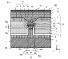
- FIG. 1 is a diagram showing a cross-sectional structure of a semiconductor laser according to Embodiment 1;
- FIG. 2 is an enlarged view around an active layer in FIG. 1;
- FIG. FIG. 2 shows an active layer of FIG. 1; It is an enlarged view around the active layer of a comparative example.
- FIG. 10 is a diagram showing a cross-sectional structure of a semiconductor laser according to a second embodiment; 6 is an enlarged view around the active layer of FIG. 5;
- FIG. FIG. 10 is a diagram showing a cross-sectional structure of a semiconductor laser according to Embodiment 3;
- 8 is a diagram showing a method of manufacturing the semiconductor laser of FIG. 7;
- FIG. 8 is a diagram showing a method of manufacturing the semiconductor laser of FIG. 7;
- FIG. 8 is a diagram showing a method of manufacturing the semiconductor laser of FIG. 7;
- FIG. 8 is a diagram showing a method of manufacturing the semiconductor laser of FIG. 7;
- FIG. 8 is a diagram showing a method of manufacturing the semiconductor laser of FIG. 7;
- FIG. 8 is a diagram showing a method of manufacturing the semiconductor laser of FIG. 7;
- FIG. 12 is a diagram showing a cross-sectional structure of a first semiconductor laser according to Embodiment 4;
- 15A and 15B are diagrams showing a method of manufacturing the semiconductor laser of FIG. 14;
- 15A and 15B are diagrams showing a method of manufacturing the semiconductor laser of FIG. 14;
- 15A and 15B are diagrams showing a method of manufacturing the semiconductor laser of FIG. 14;
- FIG. 14 is a diagram showing a method of manufacturing the semiconductor laser of FIG. 14;
- FIG. 14 is a diagram showing a method of manufacturing the semiconductor laser of FIG. 14;
- FIG. 14 is a diagram showing a method of manufacturing
- FIG. 12 is a diagram showing a cross-sectional structure of a second semiconductor laser according to Embodiment 4;
- FIG. 12 is a diagram showing a cross-sectional structure of a third semiconductor laser according to Embodiment 4;
- FIG. 12 is a diagram showing a cross-sectional structure of a semiconductor laser according to Embodiment 5;
- 21 is an enlarged view around the active layer of FIG. 20;
- FIG. FIG. 22 is a diagram showing energy bands of the extension base layer and the p-type semiconductor layer of FIG. 21;
- FIG. 12 is a diagram showing a cross-sectional structure of a semiconductor laser according to Embodiment 6;
- 24 is an enlarged view around the active layer of FIG. 23;
- FIG. 24 is a diagram showing a method of manufacturing the semiconductor laser of FIG. 23;
- FIG. 24 is a diagram showing a method of manufacturing the semiconductor laser of FIG. 23;
- FIG. 12 is a diagram showing a cross-sectional structure of a semiconductor laser according to Embodiment 7;
- 28 is an enlarged view around the active layer of FIG. 27;
- FIG. 28 is a diagram showing a method of manufacturing the semiconductor laser of FIG. 27;
- FIG. 28 is a diagram showing a method of manufacturing the semiconductor laser of FIG. 27;
- FIG. 28 is a diagram showing a method of manufacturing the semiconductor laser of FIG. 27;
- FIG. 28 is a diagram showing a method of manufacturing the semiconductor laser of FIG. 27;
- FIG. 28 is a diagram showing a method of manufacturing the semiconductor laser of FIG. 27;
- FIG. 28 is a diagram showing a method of manufacturing the semiconductor laser of FIG. 27;
- FIG. 28 is a diagram showing a method of manufacturing the semiconductor laser of FIG. 27;
- FIG. 28 is a diagram showing a method of manufacturing the semiconductor laser of FIG. 27;
- FIG. FIG. 11 is a diagram showing a method of manufacturing a semiconductor laser according to an eighth embodiment;
- FIG. 21 is a diagram showing a cross-sectional structure of a semiconductor laser according to a ninth embodiment;
- 37 is an enlarged view around the active layer of FIG. 36;
- FIG. 37 is a diagram showing a method of manufacturing the semiconductor laser of FIG. 36;
- FIG. 37 is a diagram showing a method of manufacturing the semiconductor laser of FIG. 36;
- FIG. 37 is a diagram showing a method of manufacturing the semiconductor laser of FIG. 36;
- FIG. 37 is a diagram showing a method of manufacturing the semiconductor laser of FIG. 36;
- FIG. 12 is a diagram showing a method of manufacturing a semiconductor laser according to the tenth embodiment;
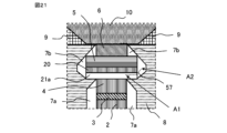
- FIG. 1 is a diagram showing a cross-sectional structure of a semiconductor laser according to Embodiment 1
- FIG. 2 is an enlarged view around the active layer in FIG.
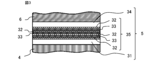
- FIG. 3 is a diagram showing the active layer of FIG. 1
- FIG. 4 is an enlarged view of the active layer and its surroundings in a comparative example.
- the semiconductor laser 100 of the first embodiment includes a first n-type clad layer 2 of n-type InP formed on the surface of an n-type semiconductor substrate 1 which is an n-type InP substrate, and one of the first n-type clad layers 2 .
- a ridge structure 16 having a portion, a diffraction grating layer 3, a second n-type clad layer 4 of n-type InP, an active layer 5, a first p-type clad layer 6 of p-type InP; p-type InP p-type semiconductor layers 7a and 7b formed on both side surfaces facing each other in the direction, and a semi-insulating layer covering both side surfaces of part of the second n-type cladding layer 4 and the p-type semiconductor layers 7a and 7b.
- a layer 10 a p-type InGaAs contact layer 11 formed on the surface of the second p-type cladding layer 10, an anode electrode 51 formed on the surface of the contact layer 11, and the side opposite to the surface of the n-type semiconductor substrate 1. and a cathode electrode 52 formed on the back surface.
- a semiconductor layer composed of the p-type semiconductor layers 7a and 7b, the semi-insulating layer 8, and the block layer 9 is a buried layer 13 buried so as to cover both sides facing each other in the direction perpendicular to the extending direction of the ridge structure 16.
- the semiconductor laser 100 shown in FIG. 1 is an example of a DFB-LD (Distributed feedback laser diode).
- the direction perpendicular to the n-type semiconductor substrate 1 is the z-direction
- the extending direction of the ridge structure 16 perpendicular to the z-direction is the y-direction
- the direction perpendicular to the z-direction and the y-direction is the x-direction.
- the first n-type clad layer 2, the diffraction grating layer 3, the second n-type clad layer 4, the active layer 5, and the first p-type clad layer 6, which constitute the ridge structure 16, are sequentially formed on the positive side in the z direction.
- Both side surfaces of the ridge structure 16 in the x direction and side surfaces of the ridge structure 16 in the x direction are referred to as both side surfaces of the ridge structure 16 and side surfaces of the ridge structure 16 as appropriate.
- the p-type semiconductor layer 7a is formed on the z-direction positive side surface of the first n-type cladding layer 2 and the side surface of the ridge structure 16 on the n-type semiconductor substrate 1 side.
- the p-type semiconductor layer 7b is formed on both side surfaces of the ridge structure 16 on the positive side in the z-direction with an isolation portion 17 separated from the p-type semiconductor layer 7a interposed therebetween.
- the region 53 in the x direction of the ridge structure 16 is between the dashed lines 54a and 54b, and the separating portion 17 is between the dashed lines 55a and 55b.
- the semi-insulating layer 8 is in contact with both side surfaces of the second n-type cladding layer 4, that is, both side surfaces in the x direction.
- the material of the diffraction grating layer 3 is a material such as InGaAsP that has a higher refractive index than InP. If the semiconductor laser 100 is not a DFB-LD, the diffraction grating layer 3 is not formed.
- the active layer 5 is generally composed of a quantum well structure and an SCH (Separate Confinement Heterostructure) structure.
- FIG. 3 shows a quantum well structure 35 in which well layers 32 and barrier layers 33 are alternately laminated, an optical confinement layer 31 formed on the side of the second n-type cladding layer 4 of the quantum well structure 35, and a first p
- the active layer 5 is shown with a light confinement layer 34 formed on the mold cladding layer 6 side.
- the quantum well structure 35 of the active layer 5 shown in FIG. 3 comprises four well layers 32 and three barrier layers 33 formed between the well layers 32 .
- the SCH structure is a structure provided with optical confinement layers 31 and 34, which are layers for confining electrons and holes in a quantum well structure 35, as shown in FIG.
- Materials for the well layer 32, the barrier layer 33, and the light confinement layers 31 and 34 are AlGaInAs, for example.
- the end of the p-type semiconductor layer 7b on the n-type semiconductor substrate 1 side is the start interface of the quantum well structure 35 of the active layer 5, that is, the optical confinement layer 31 on the second n-type cladding layer 4 side and the well formed on the surface thereof. It is preferably below the interface with layer 32 .
- the end of the separation portion 17 on the p-type semiconductor layer 7b side is located below the start interface of the quantum well structure 35 of the active layer 5 on the n-type semiconductor substrate 1 side, that is, the n-type semiconductor It is desirable to be on the substrate 1 side.
- the separation length L which is the length of the separation portion 17 in the z direction, may be long enough to block the hole current. For example, the separation length L is approximately 0.2 ⁇ m.
- a method for forming the ridge structure 16 will be described in a manufacturing method for manufacturing the semiconductor laser 100 of the third embodiment.
- the p-type semiconductor layers 7a and 7b separated by the separating portion 17 are formed, for example, as follows.
- the p-type semiconductor layers 7 a and 7 b do not grow on the side surfaces of the active layer 5 due to the formation of oxide layers on the side surfaces of the active layer 5 .
- a semiconductor layer 7 is grown.
- the p-type semiconductor layers 7a and 7b are grown without removing the oxide layer by adding hydrogen chloride.
- the p-type semiconductor layers 7 a and 7 b can be structured so as not to contact the side surfaces of the active layer 5 .
- hydrogen chloride is added to remove the oxide layer on the side surfaces of the active layer 5, and then the semi-insulating layer 8 is grown and buried.
- the p-type semiconductor layers 7a and 7b and the semi-insulating layer 8 in the buried layer 13 are formed.
- the subsequent manufacturing steps are the same as those of the third embodiment.
- a hole current flows through the semiconductor layers of semiconductor material, namely the contact layer 11, the second p-type cladding layer 10, and the first p in the ridge structure 16, via the anode electrode 51.
- the electron current is injected into the n-type cladding layer 6 and the active layer 5 and passes through the n-type semiconductor substrate 1 and the semiconductor layers of the ridge structure 16 through the cathode electrode 52, that is, the first n-type cladding layer 2, the diffraction grating layer 3, the second n-type It is implanted into the mold cladding layer 4 and the active layer 5 .
- the semiconductor laser 100 of the first embodiment generates laser light by recombination of the holes 14 and the electrons 15 in the active layer 5 .
- the hole current Ih consists of a main current I1 flowing from the first p-type cladding layer 6 to the active layer 5 and a bypass current I2 flowing from the first p-type cladding layer 6 to the active layer 5 via the p-type semiconductor layer 7b.
- the detour current I2 is a hole current component that leaks from the first p-type cladding layer 6 to the p-type semiconductor layer 7b.
- this detour current I2 cannot flow through the isolation portion 17 where the semi-insulating layer 8 exists, and flows toward the valence band of the active layer 5 having an energy level lower than the valence band of the p-type semiconductor layer 7b. Therefore, the detour current I2 is injected into the active layer 5.
- the semiconductor laser 100 of the first embodiment does not deteriorate its characteristics, that is, the optical output characteristics and the high-speed operation characteristics, even in a high-temperature environment.
- the second n-type cladding layer 4 and the semi-insulating layer 8 are in contact with each other at the separation portion 17 .
- the electron current Ie does not overflow to the semi-insulating layer 8 due to the energy barrier formed by the junction of the two.
- the semi-insulating layer 8 is an iron (Fe)-doped semi-insulating layer, for example, the electron current Ie overflow suppression performance is further improved.
- a hole current Ih for driving the semiconductor laser of the comparative example includes a main current I1 flowing from the first p-type cladding layer 6 to the active layer 5 and a main current I1 flowing from the first p-type cladding layer 6 to the p-type semiconductor layer 7. and a detour current I3 flowing through the second n-type clad layer 4 and the first n-type clad layer 2 .
- An electron current Ie for driving the semiconductor laser of the comparative example passes through the diffraction grating layer 3 and the second n-type cladding layer 4 and flows into the active layer 5 .
- the semiconductor laser of the comparative example generates laser light by recombination of holes 14 and electrons 15 in the active layer 5, like the semiconductor laser 100 of the first embodiment.
- the bypass current I3 which is part of the hole current Ih, leaks from the x-direction side surface of the first p-type cladding layer 6 to the p-type semiconductor layer 7 . Since the detour current I3 does not flow through the active layer 5 but flows through the second n-type clad layer 4 and the first n-type clad layer 2, the detour current I3 is a reactive current that does not pass through the active layer 5.
- the semiconductor laser of the comparative example since there is a reactive current that does not pass through the active layer 5, unlike the semiconductor laser 100 of the first embodiment, the characteristics of the semiconductor laser, that is, the optical output characteristics and the high-speed operation characteristics are deteriorated, resulting in a high output. Therefore, a high-speed semiconductor laser cannot be realized.
- the p-type semiconductor layer 7b arranged farther from the n-type semiconductor substrate 1 than the separation portion 17 is located in the x direction of the quantum well structure 35 in the active layer 5. Since the direction side surface is covered, a detour current I2 that is a part of the hole current Ih that has passed through the p-type semiconductor layer 7b from the first p-type cladding layer 6 can be injected into the active layer 5, and an electron current Ie never overflows from the active layer 5 . Therefore, the semiconductor laser 100 of the first embodiment can prevent a reactive current that does not pass through the active layer 5, and can improve optical output characteristics and high-speed operation performance.
- the area of the p-type layer connection portion which is the portion where the x-direction side surface of the first p-type cladding layer 6 and the p-type semiconductor layer 7 are connected, varies during the manufacturing process. If the area of the p-type layer connecting portion varies, the amount of hole current leaking to the p-type semiconductor layer 7, that is, the amount of bypass current I3, varies, and the amount of reactive current also varies. Therefore, the semiconductor laser of the comparative example has large variations in laser characteristics.
- the semiconductor laser 100 of Embodiment 1 there is a p-type layer connection portion which is a portion where the x-direction side surface of the first p-type cladding layer 6 and the p-type semiconductor layer 7b are connected.
- the p-type layer connection portion is affected by manufacturing variations, and the area of the p-type layer connection portion varies.
- the hole current Ih leaked to the p-type semiconductor layer 7b, that is, the bypass current I2 is injected into the active layer 5 and contributes to the laser operation. The characteristics do not change depending on the amount of the detour current I2.
- the semiconductor laser 100 of the first embodiment has characteristics with respect to manufacturing variations of the p-type layer connection portion, which is the portion where the x-direction side surface of the first p-type cladding layer 6 and the p-type semiconductor layer 7 are connected. Variation can be reduced.
- the semiconductor laser 100 of the first embodiment is embedded so as to cover the ridge structure 16 formed in the n-type semiconductor substrate 1 and both sides facing each other in the direction perpendicular to the extending direction of the ridge structure 16. It is a semiconductor laser with a buried layer 13 .
- the ridge structure 16 has an n-type cladding layer (second n-type cladding layer 4), an active layer 5, and a p-type cladding layer (first p-type cladding layer 6) sequentially formed from the n-type semiconductor substrate 1 side. ing.
- the buried layer 13 has a p-type semiconductor layer 7b in contact with both side surfaces of the p-type cladding layer (first p-type cladding layer 6) of the ridge structure 16 and the active layer 5, and a semi-insulating layer 8,
- the p-type semiconductor layer 7b is not in contact with the n-type clad layer (second n-type clad layer 4) of the ridge structure 16.
- the p-type cladding layer (first p-type cladding layer 6) of the ridge structure 16 and the p-type semiconductor layer 7b in contact with both side surfaces of the active layer 5 form the ridge structure 16. Since it is not in contact with the n-type clad layer (second n-type clad layer 4), ineffective current that does not pass through the active layer 5 can be prevented, and optical output characteristics and high-speed operation performance can be improved.
- the buried layer 13 is formed on both side surfaces of the n-type cladding layer (second n-type cladding layer 4) of the ridge structure 16 on the side of the n-type semiconductor substrate 1 with another p-type semiconductor layer. 7a.
- the p-type semiconductor layer 7b and the other p-type semiconductor layer 7a are separated from each other. 17 is formed, and the semi-insulating layer 8 is embedded in the isolation portion 17 .
- the semiconductor laser 100 of the first embodiment has other p-type semiconductor layers 7a on the n-type semiconductor substrate 1 side on both side surfaces of the n-type cladding layer (second n-type cladding layer 4) of the ridge structure 16. Even if there is, the p-type cladding layer (first p-type cladding layer 6) of the ridge structure 16 and the p-type semiconductor layer 7b in contact with both side surfaces of the active layer 5 are the n-type cladding layer (second n-type cladding layer) of the ridge structure 16. Since it is not in contact with layer 4), ineffective current that does not pass through active layer 5 can be prevented, and light output characteristics and high-speed operation performance can be improved.
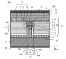
- FIG. 5 is a diagram showing a cross-sectional structure of a semiconductor laser according to Embodiment 2
- FIG. 6 is an enlarged view around the active layer in FIG.
- the p-type semiconductor layer 7 is in contact with the first p-type cladding layer 6 and the active layer 5 on both side surfaces of the ridge structure 16, and the active layer 5 of the ridge structure 16 is connected to the n-type semiconductor layer. It differs from the semiconductor laser 100 of the first embodiment in that the p-type semiconductor layer 7 is not in contact with both side surfaces of each layer on the substrate 1 side.
- FIGS. 5 and 6 show an example in which both sides of the ridge structure 16 up to a specific position of the first p-type cladding layer 6 and the active layer 5 are covered with the p-type semiconductor layer 7 .
- the specific position in FIGS. 5 and 6 is farther from the n-type semiconductor substrate 1 side than the near end of the active layer 5 on the n-type semiconductor substrate 1 side, and the n-type semiconductor substrate 1 side in the quantum well structure 35 of the active layer 5 is a position that does not reach the starting interface of the quantum well structure 35, that is, the end including the near end of the quantum well structure 35 that is on the n-type semiconductor substrate 1 side, that is, the n-type semiconductor substrate 1 side of the active layer 5 is in the middle of the light confinement layer 31.
- the p-type semiconductor layer 7 covers both sides of the quantum well structure 35 of the active layer 5 .
- the specific position of the active layer 5 may be the position of the near end of the active layer 5 on the n-type semiconductor substrate 1 side.
- the parts different from the semiconductor laser 100 of the first embodiment will be mainly described.
- semi-insulating layers 8 are formed on both side surfaces of the first n-type cladding layer 2, the diffraction grating layer 3, and the second n-type cladding layer 4 on the n-type semiconductor substrate 1 side in the ridge structure 16. in contact with In the semiconductor laser 100 of the second embodiment, as in the semiconductor laser 100 of the first embodiment, holes 14, which are majority carriers, in the contact layer 11 and the second p-type cladding layer 10 are activated when the semiconductor laser is driven. It moves to the layer 5 side and the hole current Ih flows.
- the hole current Ih consists of a main current I1 flowing from the first p-type cladding layer 6 to the active layer 5 and a bypass current I2 flowing from the first p-type cladding layer 6 to the active layer 5 via the p-type semiconductor layer 7.
- the detour current I2 is a hole current component that leaks from the first p-type cladding layer 6 to the p-type semiconductor layer 7 .
- this detour current I2 cannot flow through the side surface of the second n-type cladding layer 4 where the semi-insulating layer 8 exists, and the active layer 5 at an energy level lower than the valence band of the p-type semiconductor layer 7 is exposed.
- the detour current I2 is injected into the active layer 5 because it flows in the valence band direction.
- the semiconductor laser 100 of the second embodiment is the same as the semiconductor laser 100 of the first embodiment except that the p-type semiconductor layer 7 is not in contact with both side surfaces of each layer on the n-type semiconductor substrate 1 side from the active layer 5 of the ridge structure 16. Since it is the same, the same effect as that of the semiconductor laser 100 of the first embodiment can be obtained.
- the semiconductor laser 100 of the second embodiment is embedded so as to cover the ridge structure 16 formed in the n-type semiconductor substrate 1 and both sides facing each other in the direction perpendicular to the extending direction of the ridge structure 16. It is a semiconductor laser with a buried layer 13 .
- the ridge structure 16 has an n-type cladding layer (second n-type cladding layer 4), an active layer 5, and a p-type cladding layer (first p-type cladding layer 6) sequentially formed from the n-type semiconductor substrate 1 side. ing.
- the embedded layer 13 has a p-type semiconductor layer 7 and a semi-insulating layer 8 in contact with both side surfaces of the p-type cladding layer (first p-type cladding layer 6 ) of the ridge structure 16 and the active layer 5 .
- the p-type semiconductor layer 7 is not in contact with the n-type cladding layer (second n-type cladding layer 4) of the ridge structure 16, and the semi-insulating layer 8 is in contact with the n-type cladding layer (second n-type cladding layer 4) of the ridge structure 16. ) on both sides.
- the p-type cladding layer (first p-type cladding layer 6) of the ridge structure 16 and the p-type semiconductor layer 7 in contact with both side surfaces of the active layer 5 form the ridge structure 16. Since it is not in contact with the n-type clad layer (second n-type clad layer 4), ineffective current that does not pass through the active layer 5 can be prevented, and optical output characteristics and high-speed operation performance can be improved.
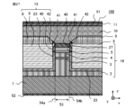
- FIG. 7 is a diagram showing a cross-sectional structure of a semiconductor laser according to Embodiment 3.
- FIG. 8 to 13 are diagrams showing a method of manufacturing the semiconductor laser of FIG.
- the ridge structure 16 has a ridge body portion 63 and ridge extension portions 64 extending in the x-direction from both side surfaces of the ridge body portion 63 , and the separating portion 17 extends from the ridge extension portions 64 . It differs from the semiconductor laser 100 of the first embodiment in that it is formed on the n-type semiconductor substrate 1 side. The parts different from the semiconductor laser 100 of the first embodiment will be mainly described.
- Embodiment 3 an example in which the ridge intermediate layer 39 in which the ridge extending portion 64 is formed is the active layer 5 will be described.
- the active layer 5 is made of a compound containing Al. The case of semiconductors has been explained.
- a method of forming p-type semiconductor layers 7a and 7b separated from each other with separation portion 17 easily even when active layer 5 does not contain Al will be described.
- FIG. 8 to 10 are diagrams for explaining the ridge structure forming process for forming the basic ridge structure 16 on the n-type semiconductor substrate 1.
- FIG. 11 illustrates extensions that etch layers other than the intermediate ridge layer 39 on both sides of the basic ridge structure 16 to form ridge extensions 64 in the intermediate ridge layer 39 extending in the x-direction from both sides of the ridge structure 16. It is a figure explaining a formation process.
- FIG. 12 illustrates a p-type semiconductor layer forming step of forming p-type semiconductor layers 7a and 7b so as to cover both side surfaces of the ridge structure 16 and the surface of the ridge extending portion 64 opposite to the n-type semiconductor substrate 1.
- FIG. 13 shows a semi-insulating layer forming step of forming a semi-insulating layer 8 so as to cover the surfaces of the p-type semiconductor layers 7a and 7b and the exposed surface of the ridge extending portion 64 on the n-type semiconductor substrate 1 side; It is a figure explaining the process of forming.
- the metal organic chemical vapor deposition (MOCVD) method is used to form the first n-type cladding layer 2, the diffraction grating layer 3, the upper part thereof, that is, the positive side in the z direction.
- the second n-type cladding layer 4, the active layer 5, and the first p-type cladding layer 6 are epitaxially grown in sequence on the surface, that is, each layer of the ridge semiconductor layer, which is the semiconductor layer of the ridge structure 16, is sequentially formed (ridge semiconductor layer forming step). ).
- An insulating film 18 of SiO 2 or the like is formed on the upper portion, ie, the surface on the z-direction positive side.
- a semiconductor laser 100 shown in FIG. 7 is an example of a DFB-LD. If the semiconductor laser 100 is not a DFB-LD, the diffraction grating layer 3 is not formed.
- the insulating film 18 is processed by etching to leave a portion for forming the basic ridge structure 16 .
- the insulating film 18 is processed using a general semiconductor photolithography process. As shown in FIG. 10, using the insulating film 18 as a mask, the first n-type clad layer 2, the diffraction grating layer 3, the second n-type clad layer 4, the active layer 5, and the first p-type clad layer 6 are removed. Etching is performed to form a basic ridge structure 16 with both x-direction side surfaces exposed.
- the width in the x direction of the basic ridge structure 16 shown in FIG. 39 is the width in the x direction.
- the ridge structure forming step for forming the basic ridge structure 16 shown in FIG. It is a step of forming
- an extending portion forming step for forming the ridge extending portion 64 is performed.
- an etchant, gas, or the like that does not etch the active layer 5 is used, and the active layer 5 is formed in the active layer main body portion 65 and the x direction of the active layer main body portion 65.
- active layer extension portions 66 extending in the x direction from both side surfaces of the ridge main portion 63 are formed. Etch each layer. Ridge extensions 64 are between dashed lines 54a and 56a and between dashed lines 56b and 54b. The ridge body portion 63 is between the dashed lines 56a and 56b.
- the ridge intermediate layer 39 is only the active layer 5
- the ridge body portion 63 is the active layer body portion 65
- the ridge extension portion 64 is also the active layer extension portion 66 .
- layers other than the ridge intermediate layer 39 on both sides of the basic ridge structure 16 in the x direction are etched.
- the surface of the active layer extending portion 66 on the side of the n-type semiconductor substrate 1 in the z-direction faces the surface of the first n-type cladding layer 2 other than the ridge main portion 63 on the side opposite to the n-type semiconductor substrate 1 .
- the layer extension 66 forms a so-called eaves.
- the active layer 5 can be shaped to have an active layer main portion 65 and an active layer extending portion 66 by using concentrated sulfuric acid for etching an InP layer, for example. can.
- the active layer 5 is formed into the active layer body 65 and the active layer by etching each layer of InP using hydrogen chloride gas in an apparatus for forming a film by the MOCVD method. It can be shaped to have extensions 66 .
- the x-direction length of the active layer extending portion 66 of the active layer 5 is set to a length that provides a shadow effect when the p-type semiconductor layer 7 is formed.
- the shadow effect means that the material gas necessary for crystal growth is not sufficiently supplied to the surface of the ridge extending portion 64 extending from the ridge main portion 63 on the n-type semiconductor substrate 1 side, that is, the surface on the negative side in the z direction. This is the effect that crystals do not grow on the surface of the extended portion 64 on the negative side in the z direction.
- a p-type semiconductor layer forming step for forming the p-type semiconductor layer 7 is performed.
- P-type semiconductor layers 7a and 7b are crystal-grown on the ridge structure 16 in the final shape shown in FIG. 11 by epitaxial growth by MOCVD.
- the shadow effect of the active layer extending portion 66, which is the ridge extending portion 64, is used to obtain the p-type semiconductor layer.
- 7a and 7b can be prevented from growing on the n-type semiconductor substrate 1 side surface of the active layer extending portion 66 which is the ridge extending portion 64.
- the p-type semiconductor layer forming step on the ridge structure 16 in the final shape shown in FIG. This can be done by forming p-type semiconductor layers 7a and 7b so as to cover them. That is, since the p-type semiconductor layer 7a and the p-type semiconductor layer 7b are separated, the p-type semiconductor layer 7a and the p-type semiconductor layer 7a are placed on the n-type semiconductor substrate 1 side of the ridge extending portion 64 where the p-type semiconductor layers 7a and 7b are not formed.
- An isolation portion 17 can be formed to isolate the p-type semiconductor layer 7b.
- a semi-insulating layer forming step of forming a semi-insulating layer 8 and a step of forming a block layer 9 are performed.
- a semi-insulating layer 8 and a block layer 9 are epitaxially grown on the intermediate product after the p-type semiconductor layer forming step shown in FIG.
- a semi-insulating layer is formed so as to cover the surfaces of the p-type semiconductor layers 7a and 7b and the exposed surface of the ridge extending portion 64 on the n-type semiconductor substrate 1 side, that is, the surface of the ridge extending portion 64 on the negative side in the z direction.
- a layer 8 is formed.
- a block layer 9 is then formed on the surface of the semi-insulating layer 8 .
- the step of forming the semi-insulating layer and the step of forming the block layer 9 are performed continuously with the step of forming the p-type semiconductor layer. That is, the p-type semiconductor layer forming step, the semi-insulating layer forming step, and the block layer 9 forming step are performed by the same apparatus.
- the insulating film 18 is removed using hydrofluoric acid, buffered hydrofluoric acid, or the like.
- the second p-type clad layer 10 and the contact layer 11 are crystal-grown by epitaxial growth.
- a second p-type clad layer 10 is formed on the surface of the block layer 9 and the surface of the ridge structure 16 , and a contact layer 11 is formed on the surface of the second p-type clad layer 10 .
- an anode electrode 51 is formed in contact with the contact layer 11, and a cathode electrode 52 is formed in contact with the back surface of the n-type semiconductor substrate 1, that is, the surface on the negative side in the z direction.
- the semiconductor laser 100 of the third embodiment has the same structure as the semiconductor laser 100 of the first embodiment. A structure in which the separated p-type semiconductor layer 7a and p-type semiconductor layer 7b are formed can be manufactured.
- the semiconductor laser 100 is embedded so as to cover the ridge structure 16 formed in the n-type semiconductor substrate 1 and both sides facing each other in the direction perpendicular to the extending direction of the ridge structure 16. It is a semiconductor laser with a buried layer 13 .
- the ridge structure 16 has an n-type cladding layer (second n-type cladding layer 4), an active layer 5, and a p-type cladding layer (first p-type cladding layer 6) sequentially formed from the n-type semiconductor substrate 1 side. ing.
- the buried layer 13 has a p-type semiconductor layer 7b in contact with both side surfaces of the p-type cladding layer (first p-type cladding layer 6) of the ridge structure 16 and the active layer 5, and a semi-insulating layer 8, The p-type semiconductor layer 7b is not in contact with the n-type clad layer (second n-type clad layer 4) of the ridge structure 16. As shown in FIG. The embedded layer 13 has other p-type semiconductor layers 7a on the n-type semiconductor substrate 1 side on both side surfaces of the n-type cladding layer (second n-type cladding layer 4) of the ridge structure 16.
- each layer of the ridge structure 16 is the z-direction, the extending direction in which the ridge structure extends is the y-direction, and the direction perpendicular to the z-direction and the y-direction is the x-direction.
- the ridge structure 16 has a ridge body portion 63 and ridge extension portions 64 extending from both side surfaces of the ridge body portion 63 in the x-direction.
- the ridge extending portion 64 is an active layer extending portion 66 in which the active layer 5 extends in the x direction.
- the p-type semiconductor layer 7b is in contact with both x-direction side surfaces of the p-type cladding layer (first p-type cladding layer 6) and the active layer 5 and the surface of the active layer extending portion 66 opposite to the n-type semiconductor substrate 1.
- the separating portion 17 is formed on the n-type semiconductor substrate 1 side of the active layer extending portion 66 .
- the semiconductor laser 100 of the third embodiment has other p-type semiconductor layers 7a on the n-type semiconductor substrate 1 side on both side surfaces of the n-type cladding layer (second n-type cladding layer 4) of the ridge structure 16.
- the p-type cladding layer (first p-type cladding layer 6) of the ridge structure 16 and the p-type semiconductor layer 7b in contact with both side surfaces of the active layer 5 are the n-type cladding layer (second n-type cladding layer) of the ridge structure 16. Since it is not in contact with layer 4), ineffective current that does not pass through active layer 5 can be prevented, and light output characteristics and high-speed operation performance can be improved.
- the ridge structure 16 formed in the n-type semiconductor substrate 1 and the ridge structure 16 are embedded so as to cover both sides facing each other in the direction perpendicular to the extending direction.
- 1 is a semiconductor laser manufacturing method for manufacturing a semiconductor laser 100 having a buried layer 13.
- FIG. The buried layer 13 has p-type semiconductor layers 7 a and 7 b and a semi-insulating layer 8 .
- each layer of the ridge structure 16 is defined as the z-direction
- the extending direction in which the ridge structure 16 extends is defined as the y-direction
- the direction perpendicular to the z-direction and the y-direction is defined as the x-direction.
- an n-type semiconductor substrate 1 is provided with an n-type cladding layer (second n-type cladding layer 4), a ridge intermediate layer 39 including an active layer 5, a p-type cladding layer (first p An n-type cladding layer (second n-type cladding layer 4), a ridge intermediate layer 39, a p-type cladding layer (first p-type cladding layer 6 ) to form a ridge structure 16.
- the semiconductor laser manufacturing method of the third embodiment after the ridge structure forming step is performed, layers other than the ridge intermediate layer 39 on both side surfaces of the ridge structure 16 are etched, and the ridge intermediate layer 39 is etched on both side surfaces of the ridge structure 16 . It includes an extending portion forming step of forming ridge extending portions 64 extending in the x direction from (both side surfaces of the ridge body portion 63 after processing). Further, in the method for manufacturing a semiconductor laser according to the third embodiment, after executing the extending portion forming step, both side surfaces of the ridge structure 16 (both side surfaces of the ridge body portion 63 and the ridge extending portion 64), the n-type semiconductor of the ridge extending portion 64 are formed.
- the p-type semiconductor layer 7a is formed on both sides of the n-type cladding layer (second n-type cladding layer 4) of the ridge structure 16 on the n-type semiconductor substrate 1 side.
- the p-type cladding layer (first p-type cladding layer 6) of the ridge structure 16 and the p-type semiconductor layer 7b in contact with both side surfaces of the active layer 5 are the n-type cladding layers (second n-type A semiconductor laser 100 can be manufactured that is not in contact with the cladding layer 4). Therefore, the semiconductor laser 100 manufactured by the method of manufacturing the semiconductor laser according to the third embodiment can prevent ineffective current not passing through the active layer 5, and can improve optical output characteristics and high-speed operation performance.
- FIG. 14 is a diagram showing the cross-sectional structure of the first semiconductor laser according to the fourth embodiment.
- 15 to 17 are diagrams showing a method of manufacturing the semiconductor laser of FIG. 18 is a diagram showing a cross-sectional structure of a second semiconductor laser according to the fourth embodiment, and
- FIG. 19 is a diagram showing a cross-sectional structure of a third semiconductor laser according to the fourth embodiment.
- the semiconductor laser 100 of the fourth embodiment differs from the semiconductor laser 100 of the third embodiment in that the ridge intermediate layer 39 of the ridge extending portion 64 in the ridge structure 16 has the extending portion base layer 21 and the active layer 5 . different.
- the parts different from the semiconductor laser 100 of the third embodiment will be mainly described.
- the first and third semiconductor lasers 100 of the fourth embodiment are examples in which the ridge intermediate layer 39 of the ridge extending portion 64 has the extending portion base layer 21, the third n-type cladding layer 20, and the active layer 5. be.
- the second semiconductor laser 100 of the fourth embodiment is an example in which the ridge intermediate layer 39 of the ridge extending portion 64 has the extending portion base layer 21 and the active layer 5 .
- the ridge structure 16 in the first semiconductor laser 100 of the fourth embodiment is an extension base of AlGaInAs or InGaAsP sequentially formed from the n-type semiconductor substrate 1 side between the second n-type cladding layer 4 and the active layer 5.
- Layer 21 has a third n-type cladding layer 20 of n-type InP.
- the material of the active layer 5 is InGaAsP or AlGaInAs
- the material of the extension base layer 21 is the same as that of the active layer 5, so the etching rate of concentrated sulfuric acid is lower than that of the InP layer.
- the ridge extension 64 can be formed using an etchant such as etchant.
- hydrogen chloride gas can be used to form the ridge extension 64 .
- the minimum thickness of the third n-type clad layer 20 is equal to or greater than the crystal lattice, for example 1 nm.
- the film thickness at which the third n-type cladding layer 20 is not etched depends on the etching material used, the state of the semiconductor layer surface during etching, and the like.
- the thickness of the third n-type cladding layer 20 need only be such that it remains even after the ridge extending portion 64 is formed by etching. If confirmation is required for the maximum film thickness at which the third n-type cladding layer 20 is not etched, the film thickness remaining after etching is confirmed by experiments.
- the extension base layer 21 may be a material other than AlGaInAs and InGaAsP as long as it is not etched by the etchant or etching gas for forming the ridge extension 64 .
- the active layer 5 and the extension base layer 21 may be in direct contact, and the lengths of the active layer 5 and the extension base layer 21 in the ridge intermediate layer 39 in the x direction are different. good too.
- the second semiconductor laser 100 of the fourth embodiment shown in FIG. 18 is an example in which the ridge intermediate layer 39 is in direct contact with the active layer 5 and the extension base layer 21 .
- FIG. 19 is an example in which the active layer 5 and the extension base layer 21 in the ridge intermediate layer 39 have different lengths in the x direction.
- FIG. 19 shows an example in which the third n-type cladding layer 20 has the same length in the x direction as the extension base layer 21 because the extension base layer 21 is shorter than the active layer 5 .
- the ridge extending portion 64 can be formed by etching.
- the ridge intermediate layer 39 has the extension base layer 21, the third n-type clad layer 20, and the active layer 5, the extension base layer 21, The third n-type cladding layer 20, the active layer 5, and the first p-type cladding layer 6 are epitaxially grown in sequence to form each layer of the ridge semiconductor layer, which is the semiconductor layer of the ridge structure 16.
- the intermediate ridge layer 39 has the extension base layer 21 and the active layer 5, the extension base layer 21, the active layer 5 and the first p-type
- the cladding layer 6 is epitaxially grown sequentially to form each layer of the ridge semiconductor layer.
- the basic ridge structure 16 is formed using the insulating film 18 as a mask, and in the extending portion forming step, the layers other than the ridge intermediate layer 39 are etched from the x direction with respect to the basic ridge structure 16, A ridge structure 16 having a ridge body portion 63 and a ridge extension portion 64 is formed.
- FIG. 15 shows an intermediate product of the first semiconductor laser 100 according to the fourth embodiment after the extending portion forming step has been completed.
- FIG. 16 shows an intermediate product of the first semiconductor laser 100 according to the fourth embodiment after the p-type semiconductor layer forming step has been completed. Since the ridge structure 16 has the ridge extending portion 64 extending from the ridge body portion 63, the shadow effect separates the p-type semiconductor layer 7a and the p-type semiconductor layer 7b on the surface of the ridge extending portion 64 on the negative side in the z direction. A portion 17 can be formed.
- FIG. 17 shows an intermediate product of the first semiconductor laser 100 according to the fourth embodiment after the semi-insulating layer forming step and the blocking layer 9 forming step have been completed and the insulating film 18 has been removed.
- the second p-type cladding layer 10 and the contact layer 11 are formed on the surface of the block layer 9 and the z-direction surface of the ridge structure 16 .
- the second p-type clad layer 10 is formed on the surface of the block layer 9 and the surface of the ridge structure 16
- the contact layer 11 is formed on the surface of the second p-type clad layer 10 .
- an anode electrode 51 is formed in contact with the contact layer 11
- a cathode electrode 52 is formed in contact with the back surface of the n-type semiconductor substrate 1, that is, the surface on the negative side in the z direction.
- the semiconductor laser 100 of the fourth embodiment has the same structure as the semiconductor laser 100 of the first embodiment, that is, the ridge structure 16 even when the active layer 5 does not contain Al.
- a structure in which the p-type semiconductor layer 7a and the p-type semiconductor layer 7b separated from each other with the separating portion 17 interposed can be formed on both side surfaces of the . Therefore, the semiconductor laser 100 of the fourth embodiment can reduce the reactive current that does not pass through the active layer 5 and improve the optical output characteristics and high-speed operation performance, compared to the semiconductor laser of the comparative example shown in FIG.
- the bypass current of the holes 14 flowing through the p-type semiconductor layer 7 is I2 is injected into the third n-type cladding layer 20 and extension base layer 21 together with the active layer 5 .
- the holes 14 and the electrons 15 recombine in the third n-type cladding layer 20 and the extension base layer 21 .
- the energy level of the valence band of the extension base layer 21 is higher than the energy level of the valence band of the p-type semiconductor layer 7b, as will be described later.
- the number of holes 14 that move from the p-type semiconductor layer 7b to the extension base layer 21 is reduced to the third nth from the p-type semiconductor layer 7b. It is much smaller than the number of holes 14 that migrate to the mold cladding layer 20 . Therefore, in the first semiconductor laser 100 of the fourth embodiment, although a reactive current is slightly generated compared to the semiconductor laser 100 of the third embodiment, the reactive current can be reduced compared to the semiconductor laser of the comparative example.
- the second semiconductor laser 100 of the fourth embodiment is more active than the first semiconductor laser 100 of the fourth embodiment because the third n-type cladding layer 20 is not provided between the active layer 5 and the extension base layer. Reactive current that does not pass through layer 5 can be reduced.
- FIG. 20 is a diagram showing a cross-sectional structure of a semiconductor laser according to Embodiment 5.
- FIG. 21 is an enlarged view of the periphery of the active layer in FIG. 20, and
- FIG. 22 is a diagram showing energy bands of the base layer and the p-type semiconductor layer of FIG.
- the extension base layer 21a of the ridge intermediate layer 39 has a valence band energy level higher than that of the extension base layer 21 of the fourth embodiment. is higher than the energy level of the semiconductor laser 100 of the fourth embodiment.
- the parts different from the semiconductor laser 100 of the fourth embodiment will be mainly described.
- the energy band shown in FIG. 22 is the energy band between the position A1 of the extension base layer 21a and the position A2 of the p-type semiconductor layer 7b shown in FIG. In FIG. 21, the pattern of the extension base layer 21a is omitted.
- the horizontal axis of FIG. 22 is position, and the vertical axis is energy [a. u. (arbitrary unit)].
- the conduction band energy 71 and the valence band energy 72 indicated by solid lines the conduction band energy 73 and the valence band energy 74 in the extension base layer 21 of the fourth embodiment are indicated by dashed lines.
- the conduction band energy and valence band energy of the third n-type cladding layer 20 are higher than the conduction band energy 73 and valence band energy 74 indicated by the dashed lines. Therefore, the energy barrier, which is the energy difference between the third n-type cladding layer 20 and the p-type semiconductor layer 7b, is smaller than the energy barrier between the extension base layers 21, 21a and the p-type semiconductor layer 7b.
- a detour current I2 of the holes 14 leaking into the p-type semiconductor layer 7b flows in the valence band side of the p-type semiconductor layer 7b. Therefore, the detour current I2 of the holes 14 flowing from the p-type semiconductor layer 7b to the ridge intermediate layer 39 mainly flows to the third n-type cladding layer 20.
- the energy level of the valence band of the p-type semiconductor layer 7b should be set to Therefore, it is necessary to increase the energy level of the valence band of the extension base layer 21 .
- the energy on the positive side of the y-axis in FIG. 22 is smaller than that of the holes 14 .
- the extension base layer 21 of the fourth embodiment is made of a highly n-type doping material, or the extension base layer 21 of the fourth embodiment is made of n having a bandgap larger than that of the p-type semiconductor layer 7b. It may be replaced with a type AlInAs layer.
- the extension base layer 21a is an n-type AlGaInAs layer or an n-type AlInAs layer, which is an n-type semiconductor layer.
- the energy level of the valence band in the extension base layer 21a of the ridge intermediate layer 39 is higher than that of the extension base layer 21 of the fourth embodiment. Since there is a higher energy barrier than in the extension base layer 21 of the fourth embodiment, the movement of the holes 14 to the extension base layer 21a is reduced, and recombination with the electrons 15 in the extension base layer 21a is reduced. Decrease. Therefore, the semiconductor laser 100 of the fifth embodiment can reduce the reactive current that does not pass through the active layer 5 more than the semiconductor laser 100 of the fourth embodiment.
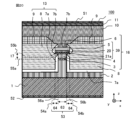
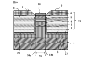
- FIG. 23 is a diagram showing a cross-sectional structure of a semiconductor laser according to Embodiment 6, and FIG. 24 is an enlarged view around the active layer in FIG. 25 and 26 are diagrams showing a method of manufacturing the semiconductor laser of FIG. 23.
- FIG. The semiconductor laser 100 of the sixth embodiment has a characteristic structure of the semiconductor laser 100 of the second embodiment, that is, the p-type semiconductor layer 7 is in contact only with the first p-type cladding layer 6 and the active layer 5 on both side surfaces of the ridge structure 16.
- the buried layer 13 has the semi-insulating layer 8, the p-type semiconductor layer 7, the semi-insulating layer 22, and the block layer 9, and the p-type semiconductor layer 7 has the semi-insulating layer 8.
- the semiconductor laser 100 of the second embodiment differs from the semiconductor laser 100 of the second embodiment in that it is formed to extend in the direction away from the ridge structure 16 on the surface opposite to the n-type semiconductor substrate 1 .
- the parts different from the semiconductor laser 100 of the second embodiment will be mainly described.
- holes 14, which are majority carriers, in the contact layer 11 and the second p-type cladding layer 10 are activated when the semiconductor laser is driven. It moves to the layer 5 side and the hole current Ih flows.
- the hole current Ih consists of a main current I1 flowing from the first p-type cladding layer 6 to the active layer 5 and a bypass current I2 flowing from the first p-type cladding layer 6 to the active layer 5 via the p-type semiconductor layer 7.
- the detour current I2 is a hole current component that leaks from the first p-type cladding layer 6 to the p-type semiconductor layer 7 .
- the p-type semiconductor layer 7 is sandwiched between the semi-insulating layer 8 and the semi-insulating layer 22 at the portion where the p-type semiconductor layer 7 extends away from the ridge structure 16, that is, in the x-direction. Since electrons 15 are not present in layer 22 , they do not recombine with holes 14 . Therefore, the bypass current I2 cannot flow through the side surfaces of the second n-type cladding layer 4 where the semi-insulating layer 8 exists, and the active layer 5 at an energy level lower than the valence band of the p-type semiconductor layer 7 is The detour current I2 is injected into the active layer 5 because it flows in the valence band direction. Therefore, in the semiconductor laser 100 of the sixth embodiment, as in the semiconductor laser 100 of the second embodiment, no reactive current is generated.
- a semiconductor laser manufacturing method for manufacturing the semiconductor laser 100 of Embodiment 6 will be described.
- the processes up to the ridge structure forming process for forming the ridge structure 16 are the same as those up to the ridge structure forming process described in the third embodiment. Since the semiconductor laser 100 of Embodiment 6 does not have the ridge extending portion 64, after the ridge structure forming step, a first semi-insulating layer 8 is formed on both sides of the ridge structure 16 on the n-type semiconductor substrate 1 side.
- a layer forming step is performed.
- a semi-insulating layer 8 is epitaxially grown so as to cover both sides of the ridge structure 16 from the n-type semiconductor substrate 1 side to a specific position of the active layer 5 .
- the specific position of the active layer 5 is the position (first specific position) of the near end of the active layer 5 on the n-type semiconductor substrate 1 side, or the n-type semiconductor substrate 1 from the near end of the active layer 5. It is a position (second specific position) that is far from the side and does not reach the near end on the n-type semiconductor substrate 1 side in the quantum well structure 35 of the active layer 5 .
- FIG. 25 shows an intermediate product of the semiconductor laser 100 after the first semi-insulating layer forming step.
- a semi-insulating layer 8 can be formed to cover both side surfaces of the layer 4 in the x direction, and a semi-insulating layer 8 can be formed to cover both side surfaces of the ridge structure 16 from the n-type semiconductor substrate 1 side to a specific position of the active layer 5 .
- a layer 8 can be formed.
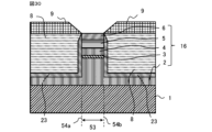
- a p-type semiconductor layer forming process for forming the p-type semiconductor layer 7 and a second semi-insulating layer forming process for forming the semi-insulating layer 22 are performed.
- p A semiconductor layer 7 is formed by epitaxial growth.
- a semi-insulating layer 22 is epitaxially grown to cover the p-type semiconductor layer 7 .
- FIG. 26 shows an intermediate product of the semiconductor laser 100 according to the sixth embodiment after the second semi-insulating layer forming step and the block layer 9 forming step are completed.
- the insulating film 18 is removed, and the second p-type cladding layer 10 and the contact layer 11 are formed on the surface of the block layer 9 and the surface of the ridge structure 16 in the z direction.
- the second p-type clad layer 10 is formed on the surface of the block layer 9 and the surface of the ridge structure 16
- the contact layer 11 is formed on the surface of the second p-type clad layer 10 .
- an anode electrode 51 is formed in contact with the contact layer 11, and a cathode electrode 52 is formed in contact with the back surface of the n-type semiconductor substrate 1, that is, the surface on the negative side in the z direction.
- the p-type semiconductor layer 7 spreads in the direction away from the ridge structure 16 on the surface of the semi-insulating layer 8 opposite to the n-type semiconductor substrate 1, and the p-type semiconductor layer 7 extends in the direction away from the ridge structure 16. Since the semiconductor laser 100 is the same as the semiconductor laser 100 of the second embodiment except that it is sandwiched between the insulating layer 8 and the semi-insulating layer 22, the same effect as the semiconductor laser 100 of the second embodiment is obtained.
- the method for manufacturing the semiconductor laser 100 according to the second embodiment shown in FIG. A step of etching the p-type semiconductor layer 7 on the positive side surface is added, and then the steps after the second semi-insulating layer forming step are performed.
- the p-type semiconductor layer 7 is etched using a semiconductor photolithography process. Since the semi-insulating layer 8 and the semi-insulating layer 22 are integrated, it can be said that the semi-insulating layer 8 is integrated.
- the method of manufacturing the semiconductor laser 100 of the second embodiment is more complicated than the method of manufacturing the semiconductor laser 100 of the sixth embodiment.
- the semiconductor laser 100 of the sixth embodiment has the characteristic structure of the semiconductor laser 100 of the second embodiment, that is, the p-type semiconductor layer 7 is formed only on the first p-type cladding layer 6 and the active layer 5 on both sides of the ridge structure 16 . are in contact with each other.
- the semiconductor laser 100 of the sixth embodiment is embedded so as to cover the ridge structure 16 formed in the n-type semiconductor substrate 1 and both sides facing each other in the direction perpendicular to the extending direction of the ridge structure 16. It is a semiconductor laser with a buried layer 13 .
- the ridge structure 16 has an n-type cladding layer (second n-type cladding layer 4), an active layer 5, and a p-type cladding layer (first p-type cladding layer 6) sequentially formed from the n-type semiconductor substrate 1 side. ing.
- the embedded layer 13 includes a p-type semiconductor layer 7 in contact with both side surfaces of the p-type cladding layer (first p-type cladding layer 6) of the ridge structure 16 and the active layer 5, a semi-insulating layer 8, and a semi-insulating layer 22. have.
- the p-type semiconductor layer 7 is not in contact with the n-type cladding layer (second n-type cladding layer 4) of the ridge structure 16, and the semi-insulating layer 8 is in contact with the n-type cladding layer (second n-type cladding layer 4) of the ridge structure 16. ) on both sides.
- the p-type semiconductor layer 7 is formed on the surface of the semi-insulating layer 8 opposite to the n-type semiconductor substrate 1 so as to extend in the direction away from the ridge structure 16 .
- a semi-insulating layer 22 covers the surface of the p-type semiconductor layer 7 opposite to the n-type semiconductor substrate 1 and the surface of the ridge structure 16 side.
- the p-type cladding layer (first p-type cladding layer 6) of the ridge structure 16 and the p-type semiconductor layer 7 in contact with both side surfaces of the active layer 5 form the ridge structure 16. Since it is not in contact with the n-type clad layer (second n-type clad layer 4), ineffective current that does not pass through the active layer 5 can be prevented, and optical output characteristics and high-speed operation performance can be improved.
- the semiconductor laser manufacturing method for manufacturing the semiconductor laser 100 according to the sixth embodiment includes a ridge structure 16 including an active layer 5 formed on an n-type semiconductor substrate 1, and both sides of the ridge structure 16 facing each other in a direction perpendicular to the extending direction of the ridge structure 16.
- This is a semiconductor laser manufacturing method for manufacturing a semiconductor laser 100 having a buried layer 13 buried so as to cover the .
- the embedded layer 13 has a first semi-insulating layer (semi-insulating layer 8), a p-type semiconductor layer 7, and a second semi-insulating layer (semi-insulating layer 22).
- the specific position of the active layer is the position of the near end of the active layer 5 on the n-type semiconductor substrate 1 side, or the quantum well of the active layer 5 farther from the n-type semiconductor substrate 1 side than the near end of the active layer 5. It is positioned so as not to reach the proximal end of the structure 35 on the side of the n-type semiconductor substrate 1 .
- an n-type cladding layer (second n-type cladding layer 4), an active layer 5, and a p-type cladding layer (first p-type cladding layer 6) are formed on an n-type semiconductor substrate 1.
- a ridge structure 16 having an n-type cladding layer (second n-type cladding layer 4), an active layer 5, and a p-type cladding layer (first p-type cladding layer 6) is sequentially formed and both side surfaces are exposed by etching.
- a ridge structure forming step is included. Furthermore, in the method of manufacturing a semiconductor laser according to the sixth embodiment, after the ridge structure forming step is performed, the first ridge is formed so as to cover both side surfaces of the ridge structure 16 from the n-type semiconductor substrate 1 side to the specific position of the active layer 5 .
- the p-type cladding layer (first p-type cladding layer 6) of the ridge structure 16 and the p-type semiconductor layer 7 in contact with both side surfaces of the active layer 5 are formed into ridges.
- a semiconductor laser 100 that is not in contact with the n-cladding layer (second n-cladding layer 4) of structure 16 can be manufactured. Therefore, the semiconductor laser 100 manufactured by the method of manufacturing the semiconductor laser according to the sixth embodiment can prevent ineffective current not passing through the active layer 5, and can improve optical output characteristics and high-speed operation performance.
- FIG. 27 is a diagram showing a cross-sectional structure of a semiconductor laser according to Embodiment 7, and FIG. 28 is an enlarged view around the active layer in FIG. 29 to 34 are diagrams showing a method of manufacturing the semiconductor laser of FIG. 27.
- This is an example of a semiconductor laser in which undoped semiconductor layers 23 are in contact with both side surfaces of each layer on the substrate 1 side.
- the undoped semiconductor layer 23 is in contact with both side surfaces of each layer from the active layer 5 of the ridge structure 16 to the n-type semiconductor substrate 1 side.
- the semiconductor of the second embodiment has the first p-type cladding layer 27 on both sides of the ridge structure 16, and the zinc-diffused semi-insulating layer 42 and the zinc-diffused block layer 41 on both side surfaces of the ridge structure 16.
- 27 and 28 show an example in which the p-type semiconductor layer 40 covers both side surfaces of the ridge structure 16 up to a specific position of the first p-type cladding layer 27 and the active layer 5 . The specific position is as described in the second embodiment.
- the parts different from the semiconductor laser 100 of the second embodiment will be mainly described.
- the p-type semiconductor layer 40 is a semiconductor layer made p-type by diffusing zinc atoms into the undoped InP semiconductor layer 23 .
- the first p-type clad layer 27 is a p-type clad layer in which zinc is diffused into the first p-type clad layer 6 of p-type InP.
- the buried layer 13 covering both sides of the ridge structure 16 has an undoped semiconductor layer 23 , a p-type semiconductor layer 40 , semi-insulating layers 8 and 42 and a block layer 9 .
- holes 14, which are majority carriers, in the contact layer 11 and the second p-type cladding layer 10 are activated when the semiconductor laser is driven. It moves to the layer 5 side and the hole current Ih flows.
- the hole current Ih consists of a main current I1 flowing from the first p-type cladding layer 27 to the active layer 5 and a bypass current I2 flowing from the first p-type cladding layer 27 to the active layer 5 via the p-type semiconductor layer 40.
- the detour current I2 is a hole current component that leaks from the first p-type cladding layer 27 to the p-type semiconductor layer 40 .
- the detour current I2 passes through the undoped semiconductor layer 23 to reach the first n-type It cannot flow to the clad layer 2 and the second n-type clad layer 4 . Therefore, in the semiconductor laser 100 of the seventh embodiment, the hole current leaked to the p-type semiconductor layer 40 is injected into the active layer 5 and does not become a reactive current as in the semiconductor laser 100 of the second embodiment. In addition, the overflow of electron current from the active layer 5 to the buried layer 13 can be suppressed by contacting the side surface of the active layer 5 with the p-type semiconductor layer 40 converted to p-type by diffusion of zinc.
- FIG. 29 shows an intermediate product of the semiconductor laser 100 according to the seventh embodiment in which the semi-insulating layer forming step and the blocking layer 9 forming step have been completed. After that, as shown in FIG. 30, the insulating film 18 is removed.
- a zinc diffusion process for diffusing zinc into a region from the far end of the undoped semiconductor layer 23 opposite to the n-type semiconductor substrate 1 to a specific position of the active layer 5 will be described.
- a diffusion prevention film 24 such as SiO 2 is formed on the surface of the block layer 9 and the z-direction surface of the ridge structure 16 , and the active layer 5 and the undoped semiconductor layer 23 in contact with the active layer 5 are formed on the diffusion prevention film 24 .
- An opening 25 is formed having a width in the x-direction inclusive. The opening 25 is processed using a semiconductor photolithography process.
- FIG. 31 An intermediate product of the semiconductor laser 100 of the seventh embodiment in which the anti-diffusion film 24 is arranged in the buried layer 13 is shown.
- a zinc oxide film (ZnO film) 26 is formed on the z-direction positive surface of the ridge structure 16 exposed by the diffusion barrier film 24 and the opening 25 and on the surface of the buried layer 13 . do.
- the intermediate product of the semiconductor laser 100 of Embodiment 7 shown in FIG. 32 is heat-treated.
- zinc (Zn) atoms in the zinc oxide film 26 are diffused into the semiconductor layer.
- Zinc atoms are present in the undoped semiconductor layer 23 and the first p-type cladding layer 6 that are in contact with both side surfaces of the ridge structure 16 from the farthest end from the n-type semiconductor substrate 1 on the positive side in the z direction to a specific position of the active layer 5 . It diffuses and becomes p-type.
- the heat treatment conditions to be set are such that, in the semiconductor layer in contact with the ridge structure 16 in the region of the opening 25, zinc atoms are diffused to specific positions in the active layer 5 toward the negative side in the z direction, and the first n-type cladding layer 2 , are heat treatment conditions under which zinc atoms do not diffuse into the undoped semiconductor layer 23 in contact with the diffraction grating layer 3 and the second n-type cladding layer 4 .
- Further set heat treatment conditions are heat treatment conditions in which zinc atoms diffuse into the first p-type cladding layer 6 but do not diffuse into the active layer 5 in the ridge structure 16 in the region of the opening 25 .
- the first p-type clad layer 6 becomes the first p-type clad layer 27 by diffusing zinc atoms.
- zinc atoms are diffused in the semiconductor layer in the region of the opening 25, that is, in the block layer 9 and the semi-insulating layer 8 on the side of the ridge structure 16, and become p-type.
- the block layer 9 and the semi-insulating layer 8 in which zinc is diffused are the semi-insulating layer 42 and the block layer 41, respectively.
- FIG. 34 shows an intermediate product of the semiconductor laser 100 according to the seventh embodiment after the heat treatment in the zinc diffusion process.
- the zinc oxide film 26 and the diffusion barrier film 24 are removed, and the second p-type clad layer 10 and contact layer 11 are formed on the surface of the block layer 9 and the surface of the ridge structure 16 in the z direction.
- the second p-type clad layer 10 is formed on the surface of the block layer 9 and the surface of the ridge structure 16
- the contact layer 11 is formed on the surface of the second p-type clad layer 10 .
- an anode electrode 51 is formed in contact with the contact layer 11, and a cathode electrode 52 is formed in contact with the back surface of the n-type semiconductor substrate 1, that is, the surface on the negative side in the z direction.
- the semiconductor laser 100 of Embodiment 7 is the same as the semiconductor laser 100 of Embodiment 2 except for the differences described above, and thus has the same effects as the semiconductor laser 100 of Embodiment 2.
- the ridge structure 16 formed in the n-type semiconductor substrate 1 and the buried substrates are embedded so as to cover both sides facing each other in the direction perpendicular to the extending direction of the ridge structure 16 .
- 1 is a semiconductor laser with an embedded layer 13.
- FIG. The ridge structure 16 has an n-type cladding layer (second n-type cladding layer 4), an active layer 5, and a p-type cladding layer (first p-type cladding layer 27) sequentially formed from the n-type semiconductor substrate 1 side. ing.
- the buried layer 13 includes a p-type cladding layer (first p-type cladding layer 27) of the ridge structure 16 and a p-type semiconductor layer 40 in contact with both side surfaces of the active layer 5, an undoped semiconductor layer 23, and a semi-insulating layer 8. , and the p-type semiconductor layer 40 is not in contact with the n-type cladding layer (second n-type cladding layer 4) of the ridge structure 16 .
- the undoped semiconductor layer 23 is in contact with both side surfaces of the n-type cladding layer (second n-type cladding layer 4) of the ridge structure 16, and the p-type semiconductor layer 40 and the p-type cladding layer (first p-type cladding layer 27) are Contains zinc.
- the p-type cladding layer (first p-type cladding layer 27) of the ridge structure 16 and the p-type semiconductor layer 40 in contact with both side surfaces of the active layer 5 form the ridge structure 16. Since it is not in contact with the n-type clad layer (second n-type clad layer 4), ineffective current that does not pass through the active layer 5 can be prevented, and optical output characteristics and high-speed operation performance can be improved.
- the ridge structure 16 including the active layer 5 formed on the n-type semiconductor substrate 1 and the two sides of the ridge structure 16 facing each other in the direction perpendicular to the extending direction of the ridge structure 16
- the buried layer 13 has an undoped semiconductor layer 23 , a p-type semiconductor layer 40 and a semi-insulating layer 8 .
- the specific position of the active layer is the position of the near end of the active layer 5 on the n-type semiconductor substrate 1 side, or the quantum well of the active layer 5 farther from the n-type semiconductor substrate 1 side than the near end of the active layer 5. It is positioned so as not to reach the proximal end of the structure 35 on the side of the n-type semiconductor substrate 1 .
- an n-type cladding layer (second n-type cladding layer 4), an active layer 5, and a p-type cladding layer (first p-type cladding layer 6) are formed on an n-type semiconductor substrate 1.
- a ridge structure 16 having an n-type cladding layer (second n-type cladding layer 4), an active layer 5, and a p-type cladding layer (first p-type cladding layer 6) is sequentially formed and both side surfaces are exposed by etching.
- a ridge structure forming step is included.
- the semiconductor laser manufacturing method of the seventh embodiment includes an undoped semiconductor layer forming step of forming an undoped semiconductor layer 23 so as to cover both side surfaces of the ridge structure 16 after executing the ridge structure forming step, and A semi-insulating layer forming step of forming a semi-insulating layer 8 so as to cover the surface, and zinc in a region from the far end of the undoped semiconductor layer 23 opposite to the n-type semiconductor substrate 1 to a specific position of the active layer 5. and a zinc diffusion step of diffusing zinc into the p-type clad layer (first p-type clad layer 6).
- the zinc-diffused p-type clad layer (first p-type clad layer 27) of the ridge structure 16 and the p-type clad layer in contact with both sides of the active layer 5 A semiconductor laser 100 in which the semiconductor layer 40 is not in contact with the n-type cladding layer (second n-type cladding layer 4) of the ridge structure 16 can be manufactured. Therefore, the semiconductor laser 100 manufactured by the semiconductor laser manufacturing method according to the seventh embodiment can prevent ineffective current not passing through the active layer 5, and can improve optical output characteristics and high-speed operation performance.
- Embodiment 8. 35A and 35B are diagrams showing a method for manufacturing a semiconductor laser according to the eighth embodiment.
- the semiconductor laser 100 of the eighth embodiment is the same as the semiconductor laser 100 of the seventh embodiment.
- the semiconductor laser manufacturing method for manufacturing the semiconductor laser 100 of the eighth embodiment differs from the semiconductor laser manufacturing method of the seventh embodiment in that zinc is diffused into the semiconductor layer by vapor phase diffusion using the MOCVD method in the zinc diffusion step. different. Mainly different parts from the semiconductor laser manufacturing method of the seventh embodiment will be described.
- the intermediate product of the semiconductor laser 100 of the eighth embodiment when zinc is diffused is the same as the intermediate product of the semiconductor laser 100 of the seventh embodiment shown in FIG.
- a diffusion barrier film 24 having 25 is disposed on the buried layer 13 .
- This intermediate product is placed in an MOCVD film forming apparatus, and dimethylzinc 28 is introduced into the apparatus.
- the dimethylzinc 28 is decomposed, and the zinc is vapor-phase diffused into the semiconductor layer through the openings 25, that is, into the semiconductor layer in the region of the openings 25.
- Diffuse zinc Predetermined pressure and temperature conditions, that is, zinc diffusion conditions, are such that the semiconductor layer in contact with the ridge structure 16 in the region of the opening 25 diffuses zinc to a specific position of the active layer 5 toward the negative side in the z direction, and , zinc does not diffuse into the undoped semiconductor layer 23 in contact with the first n-type clad layer 2 , the diffraction grating layer 3 and the second n-type clad layer 4 .
- zinc diffusion conditions are conditions under which zinc atoms diffuse into the first p-type cladding layer 6 but do not diffuse into the active layer 5 in the ridge structure 16 in the region of the opening 25 .
- the process after the zinc diffusion process is the same as the semiconductor laser manufacturing method of the seventh embodiment. Since the semiconductor laser 100 of the eighth embodiment is the same as the semiconductor laser 100 of the seventh embodiment, it has the same effects as the semiconductor laser 100 of the seventh embodiment.
- FIG. 36 is a diagram showing a cross-sectional structure of a semiconductor laser according to the ninth embodiment
- FIG. 37 is an enlarged view around the active layer of FIG. 38 to 41 are diagrams showing a method of manufacturing the semiconductor laser of FIG. 36.
- FIG. The semiconductor laser 100 of the ninth embodiment differs from the semiconductor laser 100 of the seventh embodiment in that the first p-type cladding layer 6 is formed on the positive side of the active layer 5 in the z direction.
- 36 and 37 show an example in which the p-type semiconductor layer 40 covers both side surfaces of the ridge structure 16 up to a specific position of the first p-type cladding layer 6 and the active layer 5 . The specific position is as described in the second embodiment.
- the parts different from the semiconductor laser 100 of the seventh embodiment are mainly described.
- the p-type semiconductor layer 40 is a semiconductor layer made p-type by diffusing zinc atoms into the undoped InP semiconductor layer 23 .
- the buried layer 13 covering both sides of the ridge structure 16 has an undoped semiconductor layer 23 , a p-type semiconductor layer 40 , semi-insulating layers 8 and 42 and a block layer 9 .
- majority carriers of the contact layer 11 and the second p-type clad layer 10 are used when the semiconductor laser is driven.
- Holes 14 move to the active layer 5 side, and hole current Ih flows.
- the hole current Ih consists of a main current I1 flowing from the first p-type cladding layer 6 to the active layer 5 and a bypass current I2 flowing from the first p-type cladding layer 6 to the active layer 5 via the p-type semiconductor layer 40.
- the detour current I2 is a hole current component that leaks from the first p-type cladding layer 6 to the p-type semiconductor layer 40 .
- the detour current I2 passes through the undoped semiconductor layer 23 to reach the first n-type It cannot flow to the clad layer 2 and the second n-type clad layer 4 . Therefore, in the semiconductor laser 100 of the ninth embodiment, the hole current leaked to the p-type semiconductor layer 40 is injected into the active layer 5, and the reactive current is reduced as in the semiconductor lasers 100 of the second and seventh embodiments. does not become In addition, the overflow of electron current from the active layer 5 to the buried layer 13 can be suppressed by contacting the side surface of the active layer 5 with the p-type semiconductor layer 40 converted to p-type by diffusion of zinc.
- the zinc diffusion region is limited to the portion including the undoped semiconductor layer 23. Therefore, the first p-type cladding layer 6 has Zinc is not diffused, and optical absorption loss of laser light due to zinc is suppressed. Therefore, the semiconductor laser 100 of the ninth embodiment can output laser light with a higher optical output than the semiconductor laser 100 of the seventh embodiment.
- a semiconductor laser manufacturing method for manufacturing the semiconductor laser 100 of Embodiment 9 will be described.
- the ridge structure forming step of forming the ridge structure 16, the subsequent undoped semiconductor layer forming step of forming the undoped semiconductor layer 23, the semi-insulating layer forming step of forming the semi-insulating layer 8, and the block layer 9 forming step are the same as those of the embodiment. It is the same as the semiconductor laser manufacturing method of the seventh mode.
- a zinc diffusion step is performed to diffuse zinc into the semiconductor layer.
- a diffusion prevention film 24 such as SiO 2 is formed on the surface of the block layer 9 and the surface of the ridge structure 16 in the z-direction, and an undoped semiconductor layer 23 is formed on the diffusion prevention film 24 and the active layer 5 .
- Two openings 29 are formed having a width in the x-direction including .
- the opening 29 is processed using a semiconductor photolithography process.
- FIG. 38 shows an embodiment in which diffusion preventing film 24 having opening 29 exposing a region including undoped semiconductor layer 23 on the surface of buried layer 13 opposite to n-type semiconductor substrate 1 is disposed in buried layer 13 .
- An intermediate product of the semiconductor laser 100 of form 9 is shown.
- a zinc oxide film 26 is formed on the surface of the buried layer 13 exposed by the diffusion prevention film 24 and the opening 29 .
- the intermediate manufactured body of the semiconductor laser 100 of the ninth embodiment shown in FIG. 39 is heat-treated.
- zinc atoms in the zinc oxide film 26 are diffused into the semiconductor layer.
- Zinc atoms are diffused into the undoped semiconductor layer 23 which is in contact with both sides of the ridge structure 16 from the farthest end from the n-type semiconductor substrate 1 on the positive side in the z-direction to a specific position of the active layer 5 to convert it to p-type.
- the heat treatment conditions to be set are such that the semiconductor layer in the region of the opening 29 diffuses zinc atoms to a specific position of the active layer 5 toward the z-direction negative side, and the first n-type clad layer 2 and the diffraction grating layer 3 , are heat treatment conditions under which zinc atoms do not diffuse into the undoped semiconductor layer 23 in contact with the second n-type cladding layer 4 .
- the Z zinc atoms diffuse into the semiconductor layer in the region of the opening 29, ie, the block layer 9 and the semi-insulating layer 8 on the side of the ridge structure 16, and become p-type.
- the block layer 9 and the semi-insulating layer 8 in which zinc is diffused are the semi-insulating layer 42 and the block layer 41, respectively.
- FIG. 40 shows an intermediate product of the semiconductor laser 100 of the ninth embodiment after the heat treatment in the zinc diffusion process.
- the zinc oxide film 26 and the diffusion barrier film 24 are removed, and the second p-type clad layer 10 and contact layer 11 are formed on the surface of the block layer 9 and the surface of the ridge structure 16 in the z direction.
- the second p-type clad layer 10 is formed on the surface of the block layer 9 and the surface of the ridge structure 16
- the contact layer 11 is formed on the surface of the second p-type clad layer 10 .
- an anode electrode 51 is formed in contact with the contact layer 11, and a cathode electrode 52 is formed in contact with the back surface of the n-type semiconductor substrate 1, that is, the surface on the negative side in the z direction.
- the semiconductor laser 100 of the ninth embodiment is the same as the semiconductor laser 100 of the seventh embodiment except for the differences described above, and therefore has the same effects as the semiconductor laser 100 of the seventh embodiment. Furthermore, as described above, in the semiconductor laser 100 of the ninth embodiment, zinc is not diffused into the first p-type cladding layer 6, and the light absorption loss of the laser beam due to zinc is suppressed. Compared to the semiconductor laser 100, it can output laser light with a higher optical output.
- the ridge structure 16 formed in the n-type semiconductor substrate 1 and the buried substrates are embedded so as to cover both sides facing each other in the direction perpendicular to the extending direction of the ridge structure 16 .
- 1 is a semiconductor laser with an embedded layer 13.
- FIG. The ridge structure 16 has an n-type cladding layer (second n-type cladding layer 4), an active layer 5, and a p-type cladding layer (first p-type cladding layer 6) sequentially formed from the n-type semiconductor substrate 1 side. ing.
- the embedded layer 13 includes a p-type semiconductor layer 40 in contact with both side surfaces of the p-type cladding layer (first p-type cladding layer 6) of the ridge structure 16 and the active layer 5, an undoped semiconductor layer 23, and a semi-insulating layer 8. , and the p-type semiconductor layer 40 is not in contact with the n-type cladding layer (second n-type cladding layer 4) of the ridge structure 16 .
- the undoped semiconductor layer 23 is in contact with both side surfaces of the n-type cladding layer (second n-type cladding layer 4) of the ridge structure 16, and the p-type semiconductor layer 40 contains zinc.
- the p-type cladding layer (first p-type cladding layer 6) of the ridge structure 16 and the p-type semiconductor layer 40 in contact with both side surfaces of the active layer 5 form the ridge structure 16. Since it is not in contact with the n-type clad layer (second n-type clad layer 4), ineffective current that does not pass through the active layer 5 can be prevented, and optical output characteristics and high-speed operation performance can be improved.
- a semiconductor laser manufacturing method for manufacturing the semiconductor laser 100 of the ninth embodiment includes a ridge structure 16 including an active layer 5 formed on an n-type semiconductor substrate 1, and both sides of the ridge structure 16 facing each other in a direction perpendicular to the extending direction of the ridge structure 16.
- This is a semiconductor laser manufacturing method for manufacturing a semiconductor laser 100 having a buried layer 13 buried so as to cover the .
- the buried layer 13 has an undoped semiconductor layer 23 , a p-type semiconductor layer 40 and a semi-insulating layer 8 .
- the specific position of the active layer is the position of the near end of the active layer 5 on the n-type semiconductor substrate 1 side, or the quantum well of the active layer 5 farther from the n-type semiconductor substrate 1 side than the near end of the active layer 5. It is positioned so as not to reach the proximal end of the structure 35 on the side of the n-type semiconductor substrate 1 .
- an n-type cladding layer (second n-type cladding layer 4), an active layer 5, and a p-type cladding layer (first p-type cladding layer 6) are formed on an n-type semiconductor substrate 1.
- a ridge structure 16 having an n-type cladding layer (second n-type cladding layer 4), an active layer 5, and a p-type cladding layer (first p-type cladding layer 6) is sequentially formed and both side surfaces are exposed by etching.
- a ridge structure forming step is included.
- the semiconductor laser manufacturing method of the ninth embodiment includes an undoped semiconductor layer forming step of forming an undoped semiconductor layer 23 so as to cover both side surfaces of the ridge structure 16 after executing the ridge structure forming step; A semi-insulating layer forming step of forming a semi-insulating layer 8 so as to cover the surface, and zinc in a region from the far end of the undoped semiconductor layer 23 opposite to the n-type semiconductor substrate 1 to a specific position of the active layer 5. and a zinc diffusion step to diffuse.
- the p-type cladding layer (first p-type cladding layer 27) of the ridge structure 16 and the p-type semiconductor layer 40 in contact with both side surfaces of the active layer 5 are formed into ridges.
- a semiconductor laser 100 that is not in contact with the n-cladding layer (second n-cladding layer 4) of structure 16 can be manufactured. Therefore, the semiconductor laser 100 manufactured by the semiconductor laser manufacturing method of the ninth embodiment can prevent ineffective current not passing through the active layer 5, and can improve optical output characteristics and high-speed operation performance.
- Embodiment 10. 42A and 42B are diagrams showing a method for manufacturing a semiconductor laser according to the tenth embodiment.
- the semiconductor laser 100 of the tenth embodiment is the same as the semiconductor laser 100 of the ninth embodiment.
- the semiconductor laser manufacturing method for manufacturing the semiconductor laser 100 of the tenth embodiment differs from the semiconductor laser manufacturing method of the ninth embodiment in that zinc is diffused into the semiconductor layer by vapor phase diffusion using the MOCVD method in the zinc diffusion process. different. Differences from the semiconductor laser manufacturing method of the ninth embodiment will be mainly described.
- the intermediate product of the semiconductor laser 100 of the tenth embodiment when zinc is diffused is the same as the intermediate product of the semiconductor laser 100 of the ninth embodiment shown in FIG.
- a diffusion prevention film 24 having an opening 29 for exposing a region including an undoped semiconductor layer 23 on the surface of the buried layer 13 opposite to the n-type semiconductor substrate 1 when diffusing zinc is disposed in the buried layer 13. It is This intermediate product is placed in an MOCVD film forming apparatus, and dimethylzinc 28 is introduced into the apparatus. By setting the pressure and temperature in the apparatus to predetermined conditions, the dimethylzinc 28 is decomposed, and the zinc is vapor-phase diffused into the semiconductor layer through the openings 29, that is, into the semiconductor layer in the region of the openings 29. Diffuse zinc.
- Predetermined pressure and temperature conditions that is, zinc diffusion conditions, are such that the semiconductor layer in contact with the ridge structure 16 in the region of the opening 29 diffuses zinc to a specific position of the active layer 5 toward the negative side in the z direction, and , zinc does not diffuse into the undoped semiconductor layer 23 in contact with the first n-type clad layer 2 , the diffraction grating layer 3 and the second n-type clad layer 4 .
- the process after the zinc diffusion process is the same as the semiconductor laser manufacturing method of the ninth embodiment. Since the semiconductor laser 100 of the tenth embodiment is the same as the semiconductor laser 100 of the ninth embodiment, it has the same effects as the semiconductor laser 100 of the ninth embodiment.
- the semiconductor laser 100 is not a DFB-LD as described in the first and third embodiments, the diffraction grating layer 3 is not formed.
Landscapes
- Physics & Mathematics (AREA)
- Condensed Matter Physics & Semiconductors (AREA)
- General Physics & Mathematics (AREA)
- Electromagnetism (AREA)
- Optics & Photonics (AREA)
- Geometry (AREA)
- Semiconductor Lasers (AREA)
Abstract
Description
図1は実施の形態1に係る半導体レーザの断面構造を示す図であり、図2は図1の活性層周辺の拡大図である。図3は図1の活性層を示す図であり、図4は比較例の活性層周辺の拡大図である。実施の形態1の半導体レーザ100は、n型のInP基板であるn型半導体基板1の表面に形成されたn型InPの第一n型クラッド層2と、第一n型クラッド層2の一部、回折格子層3、n型InPの第二n型クラッド層4、活性層5、p型InPの第一p型クラッド層6を有するリッジ構造16と、リッジ構造16の延伸方向に垂直な方向において互いに対向する両側面に形成されたp型InPのp型半導体層7a、7bと、第二n型クラッド層4の一部の両側面及びp型半導体層7a、7bを覆う半絶縁層8と、半絶縁層8の表面に形成されたn型InPのブロック層9と、ブロック層9の表面及び第一p型クラッド層6の表面に形成されたp型InPの第二p型クラッド層10と、第二p型クラッド層10の表面に形成されたp型InGaAsのコンタクト層11と、コンタクト層11の表面に形成されたアノード電極51と、n型半導体基板1の表面と反対側である裏面に形成されたカソード電極52と、を備えている。p型半導体層7a、7b、半絶縁層8、ブロック層9からなる半導体層は、リッジ構造16の延伸方向に垂直な方向において互いに対向する両側を覆うように埋め込まれた埋込層13である。図1に示した半導体レーザ100は、DFB-LD(Distributed feedback laser diode)の例である。n型半導体基板1に垂直な方向をz方向とし、リッジ構造16のz方向に垂直な延伸方向をy方向とし、z方向及びy方向に垂直な方向をx方向とする。リッジ構造16を構成する、第一n型クラッド層2、回折格子層3、第二n型クラッド層4、活性層5、第一p型クラッド層6は、z方向正側に順次形成されている。リッジ構造16のx方向の両側面、リッジ構造16のx方向の側面は、適宜、リッジ構造16の両側面、リッジ構造16の側面と記載する。
図5は実施の形態2に係る半導体レーザの断面構造を示す図であり、図6は図5の活性層周辺の拡大図である。実施の形態2の半導体レーザ100は、リッジ構造16の両側面においてp型半導体層7が第一p型クラッド層6及び活性層5に接しており、リッジ構造16の活性層5からn型半導体基板1側の各層の両側面にp型半導体層7が接していない点で、実施の形態1の半導体レーザ100と異なる。図5、図6では、リッジ構造16の両側面において、第一p型クラッド層6及び活性層5の特定位置までの両側面を、p型半導体層7が覆っている例を示した。図5、図6における特定位置は、活性層5におけるn型半導体基板1側の近方端よりもn型半導体基板1側から遠方で活性層5の量子井戸構造35におけるn型半導体基板1側である近方端すなわち量子井戸構造35の開始界面に至らない位置であり、量子井戸構造35におけるn型半導体基板1側である近方端を含む端すなわち活性層5のn型半導体基板1側の光閉込層31の途中の位置である。p型半導体層7は、活性層5の量子井戸構造35の両側面を覆っている。なお、活性層5の特定位置は、活性層5のn型半導体基板1側である近方端の位置でもよい。実施の形態1の半導体レーザ100と異なる部分を主に説明する。
図7は、実施の形態3に係る半導体レーザの断面構造を示す図である。図8~図13は、図7の半導体レーザの製造方法を示す図である。実施の形態3の半導体レーザ100は、リッジ構造16がリッジ本体部63とリッジ本体部63の両側面からx方向に延伸したリッジ延伸部64とを有し、分離部17がリッジ延伸部64のn型半導体基板1側に形成されている点で、実施の形態1の半導体レーザ100と異なる。実施の形態1の半導体レーザ100と異なる部分を主に説明する。
図14は、実施の形態4に係る第一の半導体レーザの断面構造を示す図である。図15~図17は、図14の半導体レーザの製造方法を示す図である。図18は実施の形態4に係る第二の半導体レーザの断面構造を示す図であり、図19は実施の形態4に係る第三の半導体レーザの断面構造を示す図である。実施の形態4の半導体レーザ100は、リッジ構造16におけるリッジ延伸部64のリッジ中間層39が延伸部土台層21、活性層5を有している点で、実施の形態3の半導体レーザ100と異なる。実施の形態3の半導体レーザ100と異なる部分を主に説明する。
図20は、実施の形態5に係る半導体レーザの断面構造を示す図である。図21は図20の活性層周辺の拡大図であり、図22は図21の延伸部土台層及びp型半導体層のエネルギーバンドを示す図である。実施の形態5の半導体レーザ100は、リッジ中間層39の延伸部土台層21aが実施の形態4の延伸部土台層21よりも、価電子帯のエネルギーレベルがp型半導体層7bの価電子帯のエネルギーレベルに対して高い点で、実施の形態4の半導体レーザ100と異なる。実施の形態4の半導体レーザ100と異なる部分を主に説明する。
図23は実施の形態6に係る半導体レーザの断面構造を示す図であり、図24は図23の活性層周辺の拡大図である。図25、図26は、図23の半導体レーザの製造方法を示す図である。実施の形態6の半導体レーザ100は、実施の形態2の半導体レーザ100の特徴構造、すなわちリッジ構造16の両側面において第一p型クラッド層6及び活性層5にのみp型半導体層7が接している構造を容易に実現できる半導体レーザである。実施の形態6の半導体レーザ100は、埋込層13が半絶縁層8、p型半導体層7、半絶縁層22、ブロック層9を有しており、p型半導体層7が半絶縁層8のn型半導体基板1と反対側の表面においてリッジ構造16から離れる方向に広がって形成されている点で、実施の形態2の半導体レーザ100と異なる。実施の形態2の半導体レーザ100と異なる部分を主に説明する。
図27は実施の形態7に係る半導体レーザの断面構造を示す図であり、図28は図27の活性層周辺の拡大図である。図29~図34は、図27の半導体レーザの製造方法を示す図である。実施の形態7の半導体レーザ100は、リッジ構造16の両側面においてp型半導体層40が第一p型クラッド層27及び活性層5に接しており、リッジ構造16の活性層5からn型半導体基板1側の各層の両側面にアンドープ半導体層23が接している半導体レーザの例である。実施の形態7の半導体レーザ100は、リッジ構造16の活性層5からn型半導体基板1側の各層の両側面にアンドープ半導体層23が接しており、リッジ構造16の活性層5のz方向正側に第一p型クラッド層27を有し、リッジ構造16の両側面側に亜鉛が拡散された半絶縁層42、亜鉛が拡散されたブロック層41を有する点で、実施の形態2の半導体レーザ100と異なる。図27、図28では、リッジ構造16の両側面において、第一p型クラッド層27及び活性層5の特定位置までの両側面を、p型半導体層40が覆っている例を示した。特定位置は実施の形態2で説明した通りである。実施の形態2の半導体レーザ100と異なる部分を主に説明する。
図35は、実施の形態8に係る半導体レーザの製造方法を示す図である。実施の形態8の半導体レーザ100は、実施の形態7の半導体レーザ100と同じである。実施の形態8の半導体レーザ100を製造する半導体レーザ製造方法は、亜鉛拡散工程においてMOCVD法を用いた気相拡散により亜鉛を半導体層に拡散させる点で、実施の形態7の半導体レーザ製造方法と異なる。実施の形態7の半導体レーザ製造方法と異なる部分を主に説明する。
図36は実施の形態9に係る半導体レーザの断面構造を示す図であり、図37は図36の活性層周辺の拡大図である。図38~図41は、図36の半導体レーザの製造方法を示す図である。実施の形態9の半導体レーザ100は、活性層5のz方向正側に第一p型クラッド層6が形成されている点で、実施の形態7の半導体レーザ100と異なる。図36、図37では、リッジ構造16の両側面において、第一p型クラッド層6及び活性層5の特定位置までの両側面を、p型半導体層40が覆っている例を示した。特定位置は実施の形態2で説明した通りである。実施の形態7の半導体レーザ100と異なる部分を主に説明する。
図42は、実施の形態10に係る半導体レーザの製造方法を示す図である。実施の形態10の半導体レーザ100は、実施の形態9の半導体レーザ100と同じである。実施の形態10の半導体レーザ100を製造する半導体レーザ製造方法は、亜鉛拡散工程においてMOCVD法を用いた気相拡散により亜鉛を半導体層に拡散させる点で、実施の形態9の半導体レーザ製造方法と異なる。実施の形態9の半導体レーザ製造方法と異なる部分を主に説明する。
Claims (24)
- n型半導体基板に形成されたリッジ構造、前記リッジ構造の延伸方向に垂直な方向において互いに対向する両側を覆うように埋め込まれた埋込層を備えた半導体レーザであって、
前記リッジ構造は、前記n型半導体基板側から順次形成されたn型クラッド層、活性層、p型クラッド層を有し、
前記埋込層は、
前記リッジ構造の前記p型クラッド層及び前記活性層の両側面に接するp型半導体層と、半絶縁層とを有し、
前記p型半導体層は、前記リッジ構造の前記n型クラッド層に接していない、
半導体レーザ。 - 前記埋込層は、前記リッジ構造の前記n型クラッド層の両側面における前記n型半導体基板側に他のp型半導体層を有しており、
前記リッジ構造の前記n型クラッド層の両側面における前記活性層側に、前記p型半導体層と前記他のp型半導体層とが分離された分離部が形成されており、
前記分離部に前記半絶縁層が埋め込まれている、
請求項1記載の半導体レーザ。 - 前記リッジ構造の前記n型クラッド層の両側面に前記半絶縁層が接している、請求項1記載の半導体レーザ。
- 前記リッジ構造の各層の積層方向をz方向とし、前記リッジ構造が延伸している延伸方向をy方向とし、前記z方向及びy方向に垂直な方向をx方向とし、
前記リッジ構造は、リッジ本体部と、リッジ本体部の両側面から前記x方向に延伸したリッジ延伸部とを有し、
前記リッジ延伸部は、前記活性層が前x方向に延伸した活性層延伸部であり、
前記p型半導体層は、前記p型クラッド層及び前記活性層の前記x方向の両側面と前記活性層延伸部の前記n型半導体基板と反対側の表面とに接しており、
前記分離部は、前記活性層延伸部の前記n型半導体基板側に形成されている、
請求項2記載の半導体レーザ。 - 前記リッジ構造の各層の積層方向をz方向とし、前記リッジ構造が延伸している延伸方向をy方向とし、前記z方向及びy方向に垂直な方向をx方向とし、
前記リッジ構造は、
前記n型クラッド層と前記活性層との間に前記n型半導体基板側から順次形成された延伸部土台層、他のn型クラッド層を有し、
かつ、リッジ本体部と、リッジ本体部の両側面から前記x方向に延伸したリッジ延伸部とを有し、
前記リッジ延伸部は、前記延伸部土台層、前記他のn型クラッド層、及び前記活性層が前x方向に延伸しており、
前記p型半導体層は、前記p型クラッド層、前記延伸部土台層、前記他のn型クラッド層、及び前記活性層の前記x方向の両側面と、前記リッジ延伸部の前記n型半導体基板と反対側の表面とに接しており、
前記分離部は、前記リッジ延伸部の前記n型半導体基板側に形成されている、
請求項2記載の半導体レーザ。 - 前記リッジ構造の各層の積層方向をz方向とし、前記リッジ構造が延伸している延伸方向をy方向とし、前記z方向及びy方向に垂直な方向をx方向とし、
前記リッジ構造は、
前記n型クラッド層と前記活性層との間に形成された延伸部土台層を有し、
かつ、リッジ本体部と、リッジ本体部の両側面から前記x方向に延伸したリッジ延伸部とを有し、
前記リッジ延伸部は、前記延伸部土台層及び前記活性層が前x方向に延伸しており、
前記p型半導体層は、前記p型クラッド層、前記延伸部土台層、及び前記活性層の前記x方向の両側面と、前記リッジ延伸部の前記n型半導体基板と反対側の表面とに接しており、
前記分離部は、前記リッジ延伸部の前記n型半導体基板側に形成されている、
請求項2記載の半導体レーザ。 - 前記延伸部土台層は、価電子帯のエネルギーレベルが前記p型半導体層の価電子帯のエネルギーレベルよりも高い、請求項5または6に記載の半導体レーザ。
- 前記延伸部土台層は、n型半導体層である、請求項7記載の半導体レーザ。
- 前記延伸部土台層は、n型AlGaInAs層又はn型AlInAs層である、請求項8記載の半導体レーザ。
- 前記埋込層は、前記n型半導体基板側に形成された前記半絶縁層と共に、他の半絶縁層を有し、
前記半絶縁層の前記n型半導体基板と反対側の表面において前記p型半導体層が前記リッジ構造から離れる方向に広がって形成されており、
前記p型半導体層における前記n型半導体基板と反対側の表面及びリッジ構造側の面を前記他の半絶縁層が覆っている、
請求項3記載の半導体レーザ。 - 前記埋込層は、アンドープ半導体層を有し、
前記アンドープ半導体層は前記リッジ構造の前記n型クラッド層の両側面に接しており、
前記p型半導体層は、亜鉛を含んでいる、
請求項1記載の半導体レーザ。 - 前記リッジ構造は、前記n型クラッド層の前記n型半導体基板側に回折格子層を介して形成された他のn型クラッド層を有している、
請求項1から11のいずれか1項に記載の半導体レーザ。 - n型半導体基板に形成されたリッジ構造、前記リッジ構造の延伸方向に垂直な方向において互いに対向する両側を覆うように埋め込まれた埋込層を備えた半導体レーザを製造する半導体レーザ製造方法であって、
前記埋込層は、p型半導体層、半絶縁層を有し、
前記リッジ構造の各層の積層方向をz方向とし、前記リッジ構造が延伸している延伸方向をy方向とし、前記z方向及びy方向に垂直な方向をx方向とし、
前記n型半導体基板に、n型クラッド層、活性層を含むリッジ中間層、p型クラッド層を順次形成し、エッチングにより両側面が露出された、前記n型クラッド層、前記リッジ中間層、前記p型クラッド層を有する前記リッジ構造を形成するリッジ構造形成工程と、
前記リッジ構造の両側面における前記リッジ中間層以外の層をエッチングし、前記リッジ中間層において前記リッジ構造の両側面から前記x方向に延伸したリッジ延伸部を形成する延伸部形成工程と、
前記リッジ構造の両側面、前記リッジ延伸部の前記n型半導体基板と反対側の表面を覆うように前記p型半導体層を形成するp型半導体層形成工程と、
前記p型半導体層の表面及び前記リッジ延伸部の前記n型半導体基板側の露出面を覆うように、前記半絶縁層を形成する半絶縁層形成工程と、
を含む、半導体レーザ製造方法。 - 前記リッジ中間層は、前記活性層のみからなっている、請求項13記載の半導体レーザ製造方法。
- 前記リッジ中間層は、前記活性層の前記n型クラッド層側に延伸部土台層を含んでいる、請求項13記載の半導体レーザ製造方法。
- 前記延伸部土台層と前記活性層との間にn型クラッド層を含んでいる、請求項15記載の半導体レーザ製造方法。
- n型半導体基板に形成された活性層を含むリッジ構造、前記リッジ構造の延伸方向に垂直な方向において互いに対向する両側を覆うように埋め込まれた埋込層を備えた半導体レーザを製造する半導体レーザ製造方法であって、
前記埋込層は、第一の半絶縁層、p型半導体層、第二の半絶縁層を有し、
前記活性層の特定位置を、
前記活性層の前記n型半導体基板側である近方端の位置又は、
前記活性層の近方端よりも前記n型半導体基板側から遠方で前記活性層の量子井戸構造における前記n型半導体基板側である近方端に至らない位置とし、
前記n型半導体基板に、n型クラッド層、前記活性層、p型クラッド層を順次形成し、エッチングにより両側面が露出された、前記n型クラッド層、前記活性層、前記p型クラッド層を有する前記リッジ構造を形成するリッジ構造形成工程と、
前記リッジ構造における前記n型半導体基板側から前記活性層の前記特定位置までの両側面を覆うように、前記第一の半絶縁層を形成する第一半絶縁層形成工程と、
前記第一の半絶縁層の表面及び前記リッジ構造の露出した前記活性層の前記特定位置から前記n型半導体基板と反対側である遠方端までの両側面を覆うように、前記p型半導体層を形成するp型半導体層形成工程と、
前記p型半導体層を覆うように、前記第二の半絶縁層を形成する第二半絶縁層形成工程と、
を含む、半導体レーザ製造方法。 - n型半導体基板に形成された活性層を含むリッジ構造、前記リッジ構造の延伸方向に垂直な方向において互いに対向する両側を覆うように埋め込まれた埋込層を備えた半導体レーザを製造する半導体レーザ製造方法であって、
前記埋込層は、アンドープ半導体層、p型半導体層、半絶縁層を有し、
前記活性層の特定位置を、
前記活性層の前記n型半導体基板側である近方端の位置又は、
前記活性層の近方端よりも前記n型半導体基板側から遠方で前記活性層の量子井戸構造における前記n型半導体基板側である近方端に至らない位置とし、
前記n型半導体基板に、n型クラッド層、前記活性層、p型クラッド層を順次形成し、エッチングにより両側面が露出された、前記n型クラッド層、前記活性層、前記p型クラッド層を有する前記リッジ構造を形成するリッジ構造形成工程と、
前記リッジ構造の両側面を覆うように前記アンドープ半導体層を形成するアンドープ半導体層形成工程と、
前記アンドープ半導体層の表面を覆うように、前記半絶縁層を形成する半絶縁層形成工程と、
前記アンドープ半導体層における前記n型半導体基板と反対側である遠方端から前記活性層の前記特定位置までの領域に亜鉛を拡散させる亜鉛拡散工程と、
を含む、半導体レーザ製造方法。 - 前記亜鉛拡散工程において、
前記リッジ構造の前記n型半導体基板と反対側の表面及び前記埋込層の前記n型半導体基板と反対側の表面における前記アンドープ半導体層を包含する領域を露出させる開口を有する拡散防止膜が前記埋込層に配置されており、
前記開口を覆うように配置された酸化亜鉛膜から前記亜鉛を前記アンドープ半導体層及び前記p型クラッド層に拡散させる、請求項18記載の半導体レーザ製造方法。 - 前記亜鉛拡散工程において、
前記リッジ構造の前記n型半導体基板と反対側の表面及び前記埋込層の前記n型半導体基板と反対側の表面における前記アンドープ半導体層を包含する領域を露出させる開口を有する拡散防止膜が前記埋込層に配置されており、
前記開口から前記アンドープ半導体層及び前記p型クラッド層に前記亜鉛を気相拡散させる、請求項18記載の半導体レーザ製造方法。 - 前記亜鉛拡散工程において、
前記埋込層の前記n型半導体基板と反対側の表面における前記アンドープ半導体層を包含する領域を露出させる開口を有する拡散防止膜が前記埋込層及び前記リッジ構造の前記n型半導体基板と反対側の表面に配置されており、
前記開口を覆うように配置された酸化亜鉛膜から前記亜鉛を前記アンドープ半導体層に拡散させる、請求項18記載の半導体レーザ製造方法。 - 前記亜鉛拡散工程において、
前記埋込層の前記n型半導体基板と反対側の表面における前記アンドープ半導体層を包含する領域を露出させる開口を有する拡散防止膜が前記埋込層及び前記リッジ構造の前記n型半導体基板と反対側の表面に配置されており、
前記開口から前記アンドープ半導体層に前記亜鉛を気相拡散させる、請求項18記載の半導体レーザ製造方法。 - 前記リッジ構造形成工程は、
前記n型半導体基板の表面に他のn型クラッド層、回折格子層を順次形成し、その後前記n型クラッド層、前記活性層を含む前記リッジ中間層、前記p型クラッド層を順次形成し、
エッチングにより両側面が露出された、前記他のn型クラッド層、前記回折格子層、前記n型クラッド層、前記リッジ中間層、前記p型クラッド層を有する前記リッジ構造を形成する、
請求項13から16のいずれか1項に記載の半導体レーザ製造方法。 - 前記リッジ構造形成工程は、
前記n型半導体基板の表面に他のn型クラッド層、回折格子層を順次形成し、その後前記n型クラッド層、前記活性層、前記p型クラッド層を順次形成し、
エッチングにより両側面が露出された、前記他のn型クラッド層、前記回折格子層、前記n型クラッド層、前記活性層、前記p型クラッド層を有する前記リッジ構造を形成する、
請求項17から22のいずれか1項に記載の半導体レーザ製造方法。
Priority Applications (5)
| Application Number | Priority Date | Filing Date | Title |
|---|---|---|---|
| CN202180104326.7A CN118266139A (zh) | 2021-11-30 | 2021-11-30 | 半导体激光器以及半导体激光器制造方法 |
| JP2023564276A JP7612050B2 (ja) | 2021-11-30 | 2021-11-30 | 半導体レーザ及び半導体レーザ製造方法 |
| PCT/JP2021/043737 WO2023100214A1 (ja) | 2021-11-30 | 2021-11-30 | 半導体レーザ及び半導体レーザ製造方法 |
| US18/697,834 US20240413613A1 (en) | 2021-11-30 | 2021-11-30 | Semiconductor laser and method for producing semiconductor laser |
| TW111143537A TWI819895B (zh) | 2021-11-30 | 2022-11-15 | 半導體雷射及半導體雷射製造方法 |
Applications Claiming Priority (1)
| Application Number | Priority Date | Filing Date | Title |
|---|---|---|---|
| PCT/JP2021/043737 WO2023100214A1 (ja) | 2021-11-30 | 2021-11-30 | 半導体レーザ及び半導体レーザ製造方法 |
Publications (1)
| Publication Number | Publication Date |
|---|---|
| WO2023100214A1 true WO2023100214A1 (ja) | 2023-06-08 |
Family
ID=86611642
Family Applications (1)
| Application Number | Title | Priority Date | Filing Date |
|---|---|---|---|
| PCT/JP2021/043737 WO2023100214A1 (ja) | 2021-11-30 | 2021-11-30 | 半導体レーザ及び半導体レーザ製造方法 |
Country Status (5)
| Country | Link |
|---|---|
| US (1) | US20240413613A1 (ja) |
| JP (1) | JP7612050B2 (ja) |
| CN (1) | CN118266139A (ja) |
| TW (1) | TWI819895B (ja) |
| WO (1) | WO2023100214A1 (ja) |
Citations (10)
| Publication number | Priority date | Publication date | Assignee | Title |
|---|---|---|---|---|
| JP2000349399A (ja) * | 1999-06-03 | 2000-12-15 | Nec Corp | 半導体光増幅器およびその製造方法 |
| US20040013143A1 (en) * | 2000-12-15 | 2004-01-22 | Springthorpe Anthony J. | Confinement layer of buried heterostructure semiconductor laser |
| WO2007072807A1 (ja) * | 2005-12-20 | 2007-06-28 | Nec Corporation | 半導体素子、および半導体素子の製造方法 |
| JP2009266891A (ja) * | 2008-04-22 | 2009-11-12 | Sumitomo Electric Ind Ltd | 半導体レーザおよびその製造方法 |
| JP2014045083A (ja) * | 2012-08-27 | 2014-03-13 | Nippon Telegr & Teleph Corp <Ntt> | 半導体光素子及び半導体光素子の作製方法 |
| JP2016031970A (ja) * | 2014-07-28 | 2016-03-07 | 三菱電機株式会社 | 光半導体装置 |
| JP2016184611A (ja) * | 2015-03-25 | 2016-10-20 | Nttエレクトロニクス株式会社 | 半導体レーザ |
| JP2018101752A (ja) * | 2016-12-21 | 2018-06-28 | 住友電気工業株式会社 | 半導体光素子およびその製造方法 |
| WO2020240644A1 (ja) * | 2019-05-27 | 2020-12-03 | 三菱電機株式会社 | 光半導体装置および光半導体装置の製造方法 |
| JP2021028971A (ja) * | 2019-08-09 | 2021-02-25 | 日本ルメンタム株式会社 | 埋め込み型半導体光素子 |
Family Cites Families (9)
| Publication number | Priority date | Publication date | Assignee | Title |
|---|---|---|---|---|
| JP2000174390A (ja) | 1998-12-08 | 2000-06-23 | Fujitsu Ltd | 半導体レーザ及びその製造方法 |
| JP3825652B2 (ja) | 2001-04-18 | 2006-09-27 | 日本電信電話株式会社 | 半導体光素子 |
| EP1251610B1 (en) * | 2001-04-18 | 2006-06-28 | Nippon Telegraph and Telephone Corporation | Semiconductor optical device and the fabrication method |
| JP2008294076A (ja) * | 2007-05-22 | 2008-12-04 | Sumitomo Electric Ind Ltd | 半導体レーザ素子 |
| JP2009283822A (ja) * | 2008-05-26 | 2009-12-03 | Mitsubishi Electric Corp | 半導体レーザ及びその製造方法 |
| JP5660940B2 (ja) | 2010-04-27 | 2015-01-28 | 住友電工デバイス・イノベーション株式会社 | 光半導体装置の製造方法 |
| JP6897928B2 (ja) * | 2016-01-14 | 2021-07-07 | 住友電工デバイス・イノベーション株式会社 | 光半導体素子の製造方法および光半導体素子 |
| US11462886B2 (en) * | 2019-08-09 | 2022-10-04 | Lumentum Japan, Inc. | Buried-type semiconductor optical device |
| CN111048993A (zh) | 2019-12-27 | 2020-04-21 | 苏州辰睿光电有限公司 | 一种微碟激光器及其制备方法 |
-
2021
- 2021-11-30 US US18/697,834 patent/US20240413613A1/en active Pending
- 2021-11-30 CN CN202180104326.7A patent/CN118266139A/zh active Pending
- 2021-11-30 WO PCT/JP2021/043737 patent/WO2023100214A1/ja active Application Filing
- 2021-11-30 JP JP2023564276A patent/JP7612050B2/ja active Active
-
2022
- 2022-11-15 TW TW111143537A patent/TWI819895B/zh active
Patent Citations (10)
| Publication number | Priority date | Publication date | Assignee | Title |
|---|---|---|---|---|
| JP2000349399A (ja) * | 1999-06-03 | 2000-12-15 | Nec Corp | 半導体光増幅器およびその製造方法 |
| US20040013143A1 (en) * | 2000-12-15 | 2004-01-22 | Springthorpe Anthony J. | Confinement layer of buried heterostructure semiconductor laser |
| WO2007072807A1 (ja) * | 2005-12-20 | 2007-06-28 | Nec Corporation | 半導体素子、および半導体素子の製造方法 |
| JP2009266891A (ja) * | 2008-04-22 | 2009-11-12 | Sumitomo Electric Ind Ltd | 半導体レーザおよびその製造方法 |
| JP2014045083A (ja) * | 2012-08-27 | 2014-03-13 | Nippon Telegr & Teleph Corp <Ntt> | 半導体光素子及び半導体光素子の作製方法 |
| JP2016031970A (ja) * | 2014-07-28 | 2016-03-07 | 三菱電機株式会社 | 光半導体装置 |
| JP2016184611A (ja) * | 2015-03-25 | 2016-10-20 | Nttエレクトロニクス株式会社 | 半導体レーザ |
| JP2018101752A (ja) * | 2016-12-21 | 2018-06-28 | 住友電気工業株式会社 | 半導体光素子およびその製造方法 |
| WO2020240644A1 (ja) * | 2019-05-27 | 2020-12-03 | 三菱電機株式会社 | 光半導体装置および光半導体装置の製造方法 |
| JP2021028971A (ja) * | 2019-08-09 | 2021-02-25 | 日本ルメンタム株式会社 | 埋め込み型半導体光素子 |
Also Published As
| Publication number | Publication date |
|---|---|
| TW202324864A (zh) | 2023-06-16 |
| JP7612050B2 (ja) | 2025-01-10 |
| CN118266139A (zh) | 2024-06-28 |
| JPWO2023100214A1 (ja) | 2023-06-08 |
| TWI819895B (zh) | 2023-10-21 |
| US20240413613A1 (en) | 2024-12-12 |
Similar Documents
| Publication | Publication Date | Title |
|---|---|---|
| US9972973B2 (en) | Process of forming semiconductor optical device and semiconductor optical device | |
| US7720123B2 (en) | Buried type semiconductor laser | |
| GB2267602A (en) | Method of making semiconductor laser | |
| US20090252190A1 (en) | Semiconductor optical device and method of fabricating the same | |
| US6556605B1 (en) | Method and device for preventing zinc/iron interaction in a semiconductor laser | |
| US5729030A (en) | Semiconductor device | |
| US7405421B2 (en) | Optical integrated device | |
| JPH07183618A (ja) | 半導体レーザ装置、半導体レーザ装置製造方法並びに集積型半導体レーザ装置 | |
| US7408965B2 (en) | Semiconductor laser diode with emission efficiency independent of thickness of p-type cladding layer | |
| WO2020240644A1 (ja) | 光半導体装置および光半導体装置の製造方法 | |
| JP7612050B2 (ja) | 半導体レーザ及び半導体レーザ製造方法 | |
| US6707834B2 (en) | Semiconductor laser device and process for producing the same | |
| US5805628A (en) | Semiconductor laser | |
| JPH07254750A (ja) | 半導体レーザ | |
| JP2002033553A (ja) | 半導体レーザ装置及びその製造方法 | |
| JPH11354886A (ja) | 半導体レーザおよびその製造方法 | |
| JP5025898B2 (ja) | 半導体レーザ素子の製造方法 | |
| JP2555984B2 (ja) | 半導体レーザおよびその製造方法 | |
| JPH01192184A (ja) | 埋込み型半導体レーザの製造方法 | |
| JP3522151B2 (ja) | 化合物半導体レーザの製造方法 | |
| JPH08316572A (ja) | レーザ装置 | |
| JPS641072B2 (ja) | ||
| KR100366697B1 (ko) | 반도체 레이저 다이오드 및 그 제조 방법 | |
| KR20210052551A (ko) | 광 반도체 장치, 및 광 반도체 장치의 제조 방법 | |
| JPH06252497A (ja) | 半導体レーザ装置およびその製造方法 |
Legal Events
| Date | Code | Title | Description |
|---|---|---|---|
| 121 | Ep: the epo has been informed by wipo that ep was designated in this application |
Ref document number: 21966301 Country of ref document: EP Kind code of ref document: A1 |
|
| WWE | Wipo information: entry into national phase |
Ref document number: 2023564276 Country of ref document: JP |
|
| WWE | Wipo information: entry into national phase |
Ref document number: 18697834 Country of ref document: US |
|
| WWE | Wipo information: entry into national phase |
Ref document number: 202180104326.7 Country of ref document: CN |
|
| NENP | Non-entry into the national phase |
Ref country code: DE |
|
| 122 | Ep: pct application non-entry in european phase |
Ref document number: 21966301 Country of ref document: EP Kind code of ref document: A1 |