WO2023095797A1 - プリント配線板 - Google Patents
プリント配線板 Download PDFInfo
- Publication number
- WO2023095797A1 WO2023095797A1 PCT/JP2022/043213 JP2022043213W WO2023095797A1 WO 2023095797 A1 WO2023095797 A1 WO 2023095797A1 JP 2022043213 W JP2022043213 W JP 2022043213W WO 2023095797 A1 WO2023095797 A1 WO 2023095797A1
- Authority
- WO
- WIPO (PCT)
- Prior art keywords
- pattern
- holes
- ground pattern
- wiring board
- printed wiring
- Prior art date
- Legal status (The legal status is an assumption and is not a legal conclusion. Google has not performed a legal analysis and makes no representation as to the accuracy of the status listed.)
- Ceased
Links
Images




Classifications
-
- H—ELECTRICITY
- H05—ELECTRIC TECHNIQUES NOT OTHERWISE PROVIDED FOR
- H05K—PRINTED CIRCUITS; CASINGS OR CONSTRUCTIONAL DETAILS OF ELECTRIC APPARATUS; MANUFACTURE OF ASSEMBLAGES OF ELECTRICAL COMPONENTS
- H05K1/00—Printed circuits
- H05K1/02—Details
-
- H—ELECTRICITY
- H05—ELECTRIC TECHNIQUES NOT OTHERWISE PROVIDED FOR
- H05K—PRINTED CIRCUITS; CASINGS OR CONSTRUCTIONAL DETAILS OF ELECTRIC APPARATUS; MANUFACTURE OF ASSEMBLAGES OF ELECTRICAL COMPONENTS
- H05K1/00—Printed circuits
- H05K1/02—Details
- H05K1/0213—Electrical arrangements not otherwise provided for
- H05K1/0216—Reduction of cross-talk, noise or electromagnetic interference
- H05K1/0218—Reduction of cross-talk, noise or electromagnetic interference by printed shielding conductors, ground planes or power plane
-
- H—ELECTRICITY
- H01—ELECTRIC ELEMENTS
- H01P—WAVEGUIDES; RESONATORS, LINES, OR OTHER DEVICES OF THE WAVEGUIDE TYPE
- H01P3/00—Waveguides; Transmission lines of the waveguide type
- H01P3/02—Waveguides; Transmission lines of the waveguide type with two longitudinal conductors
- H01P3/08—Microstrips; Strip lines
-
- H—ELECTRICITY
- H05—ELECTRIC TECHNIQUES NOT OTHERWISE PROVIDED FOR
- H05K—PRINTED CIRCUITS; CASINGS OR CONSTRUCTIONAL DETAILS OF ELECTRIC APPARATUS; MANUFACTURE OF ASSEMBLAGES OF ELECTRICAL COMPONENTS
- H05K1/00—Printed circuits
- H05K1/02—Details
- H05K1/0296—Conductive pattern lay-out details not covered by sub groups H05K1/02 - H05K1/0295
- H05K1/0298—Multilayer circuits
-
- H—ELECTRICITY
- H05—ELECTRIC TECHNIQUES NOT OTHERWISE PROVIDED FOR
- H05K—PRINTED CIRCUITS; CASINGS OR CONSTRUCTIONAL DETAILS OF ELECTRIC APPARATUS; MANUFACTURE OF ASSEMBLAGES OF ELECTRICAL COMPONENTS
- H05K3/00—Apparatus or processes for manufacturing printed circuits
- H05K3/0011—Working of insulating substrates or insulating layers
- H05K3/0017—Etching of the substrate by chemical or physical means
- H05K3/0026—Etching of the substrate by chemical or physical means by laser ablation
-
- H—ELECTRICITY
- H05—ELECTRIC TECHNIQUES NOT OTHERWISE PROVIDED FOR
- H05K—PRINTED CIRCUITS; CASINGS OR CONSTRUCTIONAL DETAILS OF ELECTRIC APPARATUS; MANUFACTURE OF ASSEMBLAGES OF ELECTRICAL COMPONENTS
- H05K3/00—Apparatus or processes for manufacturing printed circuits
- H05K3/46—Manufacturing multilayer circuits
-
- H—ELECTRICITY
- H05—ELECTRIC TECHNIQUES NOT OTHERWISE PROVIDED FOR
- H05K—PRINTED CIRCUITS; CASINGS OR CONSTRUCTIONAL DETAILS OF ELECTRIC APPARATUS; MANUFACTURE OF ASSEMBLAGES OF ELECTRICAL COMPONENTS
- H05K3/00—Apparatus or processes for manufacturing printed circuits
- H05K3/46—Manufacturing multilayer circuits
- H05K3/4644—Manufacturing multilayer circuits by building the multilayer layer by layer, i.e. build-up multilayer circuits
- H05K3/4661—Adding a circuit layer by direct wet plating, e.g. electroless plating; insulating materials adapted therefor
-
- H—ELECTRICITY
- H05—ELECTRIC TECHNIQUES NOT OTHERWISE PROVIDED FOR
- H05K—PRINTED CIRCUITS; CASINGS OR CONSTRUCTIONAL DETAILS OF ELECTRIC APPARATUS; MANUFACTURE OF ASSEMBLAGES OF ELECTRICAL COMPONENTS
- H05K2201/00—Indexing scheme relating to printed circuits covered by H05K1/00
- H05K2201/09—Shape and layout
- H05K2201/09209—Shape and layout details of conductors
- H05K2201/09218—Conductive traces
- H05K2201/09227—Layout details of a plurality of traces, e.g. escape layout for Ball Grid Array [BGA] mounting
-
- H—ELECTRICITY
- H05—ELECTRIC TECHNIQUES NOT OTHERWISE PROVIDED FOR
- H05K—PRINTED CIRCUITS; CASINGS OR CONSTRUCTIONAL DETAILS OF ELECTRIC APPARATUS; MANUFACTURE OF ASSEMBLAGES OF ELECTRICAL COMPONENTS
- H05K2201/00—Indexing scheme relating to printed circuits covered by H05K1/00
- H05K2201/09—Shape and layout
- H05K2201/09209—Shape and layout details of conductors
- H05K2201/09218—Conductive traces
- H05K2201/09236—Parallel layout
-
- H—ELECTRICITY
- H05—ELECTRIC TECHNIQUES NOT OTHERWISE PROVIDED FOR
- H05K—PRINTED CIRCUITS; CASINGS OR CONSTRUCTIONAL DETAILS OF ELECTRIC APPARATUS; MANUFACTURE OF ASSEMBLAGES OF ELECTRICAL COMPONENTS
- H05K2201/00—Indexing scheme relating to printed circuits covered by H05K1/00
- H05K2201/09—Shape and layout
- H05K2201/09209—Shape and layout details of conductors
- H05K2201/095—Conductive through-holes or vias
- H05K2201/09545—Plated through-holes or blind vias without lands
-
- H—ELECTRICITY
- H05—ELECTRIC TECHNIQUES NOT OTHERWISE PROVIDED FOR
- H05K—PRINTED CIRCUITS; CASINGS OR CONSTRUCTIONAL DETAILS OF ELECTRIC APPARATUS; MANUFACTURE OF ASSEMBLAGES OF ELECTRICAL COMPONENTS
- H05K2201/00—Indexing scheme relating to printed circuits covered by H05K1/00
- H05K2201/09—Shape and layout
- H05K2201/09209—Shape and layout details of conductors
- H05K2201/095—Conductive through-holes or vias
- H05K2201/09609—Via grid, i.e. two-dimensional array of vias or holes in a single plane
-
- H—ELECTRICITY
- H05—ELECTRIC TECHNIQUES NOT OTHERWISE PROVIDED FOR
- H05K—PRINTED CIRCUITS; CASINGS OR CONSTRUCTIONAL DETAILS OF ELECTRIC APPARATUS; MANUFACTURE OF ASSEMBLAGES OF ELECTRICAL COMPONENTS
- H05K2201/00—Indexing scheme relating to printed circuits covered by H05K1/00
- H05K2201/09—Shape and layout
- H05K2201/09209—Shape and layout details of conductors
- H05K2201/095—Conductive through-holes or vias
- H05K2201/09618—Via fence, i.e. one-dimensional array of vias
Definitions
- Patent Document 1 A wiring board is described in Japanese Patent Application Laid-Open No. 2006-24618 (Patent Document 1).
- the wiring board described in Patent Document 1 includes a first dielectric layer, a first wiring pattern, a second wiring pattern and a coplanar ground pattern, a second dielectric layer, a first ground pattern and a second ground pattern. , and a conductor layer.
- the first dielectric layer has a first principal surface and a second principal surface opposite to the first principal surface.
- the first wiring pattern, the second wiring pattern and the coplanar ground pattern are arranged on the second main surface.
- the first wiring pattern, the second wiring pattern and the coplanar ground pattern extend along the first direction.
- the coplanar ground pattern is arranged between the first wiring pattern and the second wiring pattern in a second direction perpendicular to the first direction.
- the second dielectric layer is arranged on the second main surface so as to cover the first wiring pattern, the second wiring pattern and the coplanar ground pattern.
- the second dielectric layer has a third main surface facing the second main surface and a fourth main surface opposite to the third main surface.
- the first ground pattern and the second ground pattern are arranged on the first main surface and the fourth main surface, respectively.
- a plurality of through holes are formed in the wiring board described in Patent Document 1.
- the plurality of through holes are arranged along the first direction in plan view.
- the through hole penetrates the first dielectric layer, the second dielectric layer and the coplanar ground pattern.
- the through hole is circular in plan view.
- the through hole is filled with a conductor layer.
- the conductor layer electrically connects the coplanar ground pattern to the first ground pattern and the second ground pattern. In the wiring board described in Patent Document 1, crosstalk between the first wiring pattern and the second wiring pattern is suppressed by the conductor layer.
- a printed wiring board of the present disclosure includes a first insulating layer having a first main surface and a second main surface opposite to the first main surface; A first wiring pattern, a second wiring pattern, and a first ground pattern extending along one direction, and a second ground pattern, the first wiring pattern, and the second wiring, which are arranged on the first main surface.
- the first ground pattern is between the first wiring pattern and the second wiring pattern in a second direction orthogonal to the first direction, and is separated from the first wiring pattern and the second wiring pattern.
- a plurality of first through holes are formed penetrating the layer, the second insulating layer and the second ground pattern. The plurality of first through-holes are arranged at intervals so as to form a row along the first direction.
- the first conductor layer is arranged on the inner wall surface of each of the plurality of first through holes and electrically connected to the first ground pattern, the second ground pattern and the third ground pattern.
- Each of the plurality of first through holes has a width in the first direction that is greater than the width in the second direction.
- FIG. 1 is a plan view of a printed wiring board 100.
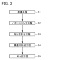
- FIG. FIG. 2 is a cross-sectional view along II-II in FIG. 3A to 3C are process diagrams showing a method for manufacturing printed wiring board 100.
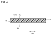
- FIG. 4 is a cross-sectional view for explaining the preparation step S1.
- FIG. 5 is a cross-sectional view for explaining the patterning step S2.
- FIG. 6 is a cross-sectional view for explaining the bonding step S3.
- FIG. 7 is a cross-sectional view for explaining the through-hole forming step S4.
- FIG. 8 is a plan view of printed wiring board 200 .
- 9 is a cross-sectional view taken along line IX-IX in FIG. 8.
- FIG. 10 is a plan view of printed wiring board 100A.
- FIG. 11 is a cross-sectional view along XI-XI in FIG. 12 is a cross-sectional view taken along line XII-XII in FIG. 10.
- FIG. 13 is a plan view of printed wiring board 100B.
- FIG. 14 is a plan view of printed wiring board 100C.
- the present disclosure has been made in view of the problems of the prior art as described above. More specifically, the present disclosure provides a printed wiring board capable of suppressing crosstalk between the first wiring pattern and the second wiring pattern.
- a printed wiring board includes a first insulating layer having a first main surface and a second main surface opposite to the first main surface, a first insulating layer disposed on the second main surface, and A first wiring pattern, a second wiring pattern, and a first ground pattern extending along a first direction in plan view, and a second ground pattern and the first wiring pattern disposed on the first main surface.
- an adhesive layer arranged on the second main surface so as to cover the second wiring pattern and the first ground pattern; a third main surface arranged on the adhesive layer and facing the adhesive layer;
- a second insulating layer having a fourth main surface opposite to the third main surface, a third ground pattern disposed on the fourth main surface, and a first conductor layer.
- the first ground pattern is between the first wiring pattern and the second wiring pattern in a second direction orthogonal to the first direction and is separated from the first wiring pattern and the second wiring pattern.
- a plurality of first through holes are formed through the layer, the second insulating layer and the third ground pattern. The plurality of first through-holes are arranged at intervals so as to form a row along the first direction.
- the first conductor layer is arranged on the inner wall surface of each of the plurality of first through holes and electrically connected to the first ground pattern, the second ground pattern and the third ground pattern.
- Each of the plurality of first through holes has a width in the first direction that is greater than the width in the second direction.
- each of the plurality of first through holes may extend along the first direction in plan view.
- the printed wiring board of (1) above may further include a second conductor layer.
- a plurality of second through holes may be formed through the layer, the second insulating layer and the third ground pattern.
- the plurality of second through holes may be arranged at intervals so as to form a row along the first direction between the row of the plurality of first through holes and the second wiring pattern. Each of the plurality of second through holes may be displaced from each of the plurality of first through holes in the first direction.
- the second conductor layer may be arranged on the inner wall surface of each of the plurality of second through holes and electrically connected to the first ground pattern, the second ground pattern and the third ground pattern.
- Each of the plurality of second through holes may have a width in the first direction greater than a width in the second direction.
- each of the plurality of first through holes and each of the plurality of second through holes may extend along the first direction in plan view. .
- each of the plurality of first through holes and each of the plurality of second through holes are first portions extending along the first direction in plan view. and a second portion connected to the center of the first portion in the first direction.
- the second portion may extend from the first portion along the direction from the first wiring pattern side to the second wiring pattern side.
- the second portion may extend from the first portion along the direction from the second wiring pattern side to the first wiring pattern side.
- each of the plurality of first through holes and each of the plurality of second through holes extend linearly in a plan view, the third portion and the fourth portion.
- the third portion and the fourth portion may have One end of the third portion and one end of the fourth portion may be connected to each other.
- the one end of the third portion may be located on the one side in the first direction with respect to the other end of the third portion.
- the one end of the fourth portion may be on the other side in the first direction than the other end of the fourth portion.
- In each of the plurality of first through holes even if the other end of the third portion and the other end of the fourth portion are closer to the second wiring pattern than the one end of the third portion and the one end of the fourth portion, respectively good.
- In each of the plurality of second through holes even if the other end of the third portion and the other end of the fourth portion are closer to the first wiring pattern than the one end of the third portion and the one end of the fourth portion, respectively good.
- a printed wiring board according to the first embodiment will be described.
- a printed wiring board according to the first embodiment is referred to as a printed wiring board 100 .
- FIG. 1 is a plan view of the printed wiring board 100.
- FIG. FIG. 2 is a cross-sectional view along II-II in FIG.
- the printed wiring board 100 includes a first insulating layer 10, a first wiring pattern 21, a second wiring pattern 22 and a first ground pattern 23, a second ground pattern 30, It has an adhesive layer 40 , a second insulating layer 50 , a third ground pattern 60 and a first conductor layer 70 .
- the first insulating layer 10 is made of an electrically insulating material.
- the first insulating layer 10 is made of polyimide, fluorine resin, or the like, for example.
- the first insulating layer 10 has a first major surface 10a and a second major surface 10b.
- the first main surface 10a and the second main surface 10b are end surfaces in the thickness direction of the first insulating layer 10 .
- the second principal surface 10b is the opposite surface of the first principal surface 10a.
- the first wiring pattern 21, the second wiring pattern 22 and the first ground pattern 23 are arranged on the second main surface 10b.
- the first wiring pattern 21, the second wiring pattern 22 and the first ground pattern 23 are made of an electrically conductive material.
- the first wiring pattern 21, the second wiring pattern 22 and the first ground pattern 23 are made of copper, for example.
- the first wiring pattern 21, the second wiring pattern 22, and the first ground pattern 23 extend along the first direction DR1 in plan view.
- the first ground pattern 23 is between the first wiring pattern 21 and the second wiring pattern 22 and is separated from the first wiring pattern 21 and the second wiring pattern 22 in the second direction DR2.
- the second direction DR2 is a direction orthogonal to the first direction DR1.
- the width of the first ground pattern 23 in the second direction DR2 is preferably larger than the width of the first wiring pattern 21 in the second direction DR2 and the width of the second wiring pattern 22 in the second direction DR2.
- the second ground pattern 30 is made of an electrically conductive material.
- the second ground pattern 30 is made of copper, for example.
- the second ground pattern 30 is arranged on the first main surface 10a.
- the second ground pattern 30 overlaps the first wiring pattern 21, the second wiring pattern 22 and the first ground pattern 23 in plan view.
- the second ground pattern 30 preferably covers the entire first main surface 10a.
- the adhesive layer 40 is made of, for example, a thermosetting resin material such as epoxy resin.
- the adhesive layer 40 is arranged on the second main surface 10 b so as to cover the first wiring pattern 21 , the second wiring pattern 22 and the first ground pattern 23 .
- the second insulating layer 50 is made of an electrically insulating material.
- the second insulating layer 50 is made of, for example, polyimide, fluorine resin, or the like.
- the second insulating layer 50 is preferably made of the same material as the first insulating layer 10 .
- the second insulating layer 50 has a third main surface 50a and a fourth main surface 50b.
- the third main surface 50a and the fourth main surface 50b are end surfaces in the thickness direction of the second insulating layer 50 .
- the third main surface 50a faces the adhesive layer 40 side.
- the fourth principal surface 50b is the opposite surface of the third principal surface 50a.
- the third ground pattern 60 is made of an electrically conductive material.
- the third ground pattern 60 is made of copper, for example.
- the third ground pattern 60 is arranged on the fourth main surface 50b.
- the third ground pattern 60 overlaps the first wiring pattern 21, the second wiring pattern 22 and the first ground pattern 23 in plan view.
- the third ground pattern 60 preferably covers the entire fourth main surface 50b.
- a plurality of first through holes 10 c are formed in the first insulating layer 10 , first ground pattern 23 , second ground pattern 30 , adhesive layer 40 , second insulating layer 50 and third ground pattern 60 .
- the first through hole 10c penetrates the first insulating layer 10, the first ground pattern 23, the second ground pattern 30, the adhesive layer 40, the second insulating layer 50 and the third ground pattern 60 in the thickness direction.
- the plurality of first through holes 10c are arranged in a row along the first direction DR1 at intervals in plan view.
- the interval between the first through holes 10c adjacent in the first direction DR1 is constant, for example.
- the width of the first through hole 10c in the first direction DR1 is greater than the width of the first through hole 10c in the second direction DR2.
- the first through hole 10c extends, for example, along the first direction DR1.
- the first through hole 10c preferably has an oval shape whose longitudinal direction is along the first direction DR1 in plan view.
- the first conductor layer 70 is a layer formed by plating, for example.
- the first conductor layer 70 is made of copper, for example.
- the first conductor layer 70 is arranged on the inner wall surface of the first through hole 10c.
- the first conductor layer 70 may be filled in the first through hole 10c.
- the first conductor layer 70 electrically connects the first ground pattern 23, the second ground pattern 30, and the third ground pattern 60 to each other.
- FIG. 3 is a process diagram showing a method for manufacturing the printed wiring board 100.
- the method for manufacturing printed wiring board 100 includes preparation step S1, patterning step S2, bonding step S3, through-hole forming step S4, and plating step S5.
- FIG. 4 is a cross-sectional view explaining the preparation step S1.
- the first insulating layer 10 is prepared in the preparation step S1.
- a copper foil 31 and a copper foil 24 are respectively arranged on the first main surface 10a and the second main surface 10b of the first insulating layer 10 prepared in the preparation step S1. Note that the copper foil 31 becomes the second ground pattern 30 .
- FIG. 5 is a cross-sectional view explaining the patterning step S2. As shown in FIG. 5, in the patterning step S2, the copper foil 24 is patterned to form the first wiring pattern 21, the second wiring pattern 22 and the first ground pattern 23. As shown in FIG. 5, in the patterning step S2, the copper foil 24 is patterned to form the first wiring pattern 21, the second wiring pattern 22 and the first ground pattern 23. As shown in FIG. 5, in the patterning step S2, the copper foil 24 is patterned to form the first wiring pattern 21, the second wiring pattern 22 and the first ground pattern 23. As shown in FIG.
- the copper foil 24 In the patterning of the copper foil 24, first, for example, a dry film resist is attached on the copper foil 24. Second, the applied dry film resist is developed and exposed. Thirdly, the first wiring pattern 21, the second wiring pattern 22 and the first ground pattern 23 are formed by etching the copper foil 24 using the developed and exposed dry film resist as a mask.
- FIG. 6 is a cross-sectional view for explaining the bonding step S3.
- the second insulating layer 50 having the copper foil 61 disposed on the fourth main surface 50b is attached to the first insulating layer 10 using the adhesive layer 40. be.
- the copper foil 61 becomes the third ground pattern 60 .
- FIG. 7 is a cross-sectional view for explaining the through-hole forming step S4.
- the first through-holes 10c are formed.
- the first through holes 10c are formed by, for example, irradiating laser light.
- plating step S5 plating is performed to form the first conductor layer 70 on the inner wall surface of the first through hole 10c.
- This plating is performed by an electroless plating method or an electrolytic plating method.
- the printed wiring board 100 having the structure shown in FIGS. 1 and 2 is manufactured.
- the first wiring pattern 21 and the second wiring pattern 22 When signals are transmitted through the first wiring pattern 21 and the second wiring pattern 22 (when current flows through the first wiring pattern 21 and the second wiring pattern 22), the first wiring pattern 21 and the second wiring pattern 22 emits electromagnetic waves.
- the electromagnetic wave radiated from the first wiring pattern 21 becomes noise for the signal transmitted through the second wiring pattern 22, and the electromagnetic wave radiated from the second wiring pattern 22 becomes noise for the signal transmitted through the first wiring pattern 21. . That is, crosstalk occurs between the first wiring pattern 21 and the second wiring pattern 22 .
- the first conductor layer 70 is electrically connected to the first ground pattern 23 , the second ground pattern 30 and the third ground pattern 60 . Therefore, in printed wiring board 100, part of the electromagnetic waves radiated from first wiring pattern 21 and directed to second wiring pattern 22 and part of the electromagnetic waves radiated from second wiring pattern 22 and directed to first wiring pattern 21 part is blocked by the first conductor layer 70 arranged on the inner wall surface of the first through hole 10c.
- the width of first through-hole 10c in first direction DR1 is greater than the width of first through-hole 10c in second direction DR2.
- the first through holes 10c can be densely formed in the first direction DR1 without reducing the interval.
- crosstalk between first wiring pattern 21 and second wiring pattern 22 is suppressed.
- FIG. 8 is a plan view of printed wiring board 200 .
- 9 is a cross-sectional view taken along line IX-IX in FIG. 8.
- the printed wiring board 200 includes a first insulating layer 10, a first wiring pattern 21, a second wiring pattern 22 and a first ground pattern 23, a second ground pattern 30, It has an adhesive layer 40 , a second insulating layer 50 , a third ground pattern 60 and a first conductor layer 70 .
- the first through holes 10c are circular in plan view. That is, in printed wiring board 200, the width of first through hole 10c in second direction DR2 is equal to the width of first through hole 10c in first direction DR1.
- part of the electromagnetic wave radiated from the first wiring pattern 21 and directed to the second wiring pattern 22 and part of the electromagnetic wave radiated from the second wiring pattern 22 and directed to the first wiring pattern 21 are Crosstalk between the first wiring pattern 21 and the second wiring pattern 22 is suppressed because it is shielded by the first conductor layer 70 arranged on the inner wall surface of the first through hole 10c.
- a printed wiring board according to the second embodiment will be described.
- a printed wiring board according to the second embodiment is referred to as a printed wiring board 100A.
- points different from printed wiring board 100 will be mainly described, and redundant description will not be repeated.
- FIG. 10 is a plan view of the printed wiring board 100A.
- FIG. 11 is a cross-sectional view along XI-XI in FIG. 12 is a cross-sectional view taken along line XII-XII in FIG. 10.
- FIG. 10A includes first insulating layer 10, first wiring pattern 21, second wiring pattern 22 and first ground pattern 23, and second ground pattern. 30 , an adhesive layer 40 , a second insulating layer 50 , a third ground pattern 60 and a first conductor layer 70 .
- the configuration of printed wiring board 100A is common to the configuration of printed wiring board 100 .
- the printed wiring board 100A further has a second conductor layer 80 .
- a plurality of second through holes 10d are formed in first insulating layer 10, first ground pattern 23, second ground pattern 30, adhesive layer 40, second insulating layer 50 and third ground pattern 60. It is
- the second through hole 10d penetrates the first insulating layer 10, the first ground pattern 23, the second ground pattern 30, the adhesive layer 40, the second insulating layer 50 and the third ground pattern 60 in the thickness direction.
- the plurality of second through holes 10d are arranged at intervals so as to form a row along the first direction DR1.
- the interval between two adjacent second through holes 10d is constant, for example.
- the row of the second through holes 10d is arranged between the row of the first through holes 10c and the second wiring pattern 22 in plan view.
- the position of the second through hole 10d in the first direction DR1 is shifted from the position of the first through hole 10c in the first direction DR1.
- the width of the second through hole 10d in the first direction DR1 is greater than the width of the second through hole 10d in the second direction DR2.
- the second through hole 10d extends, for example, along the first direction DR1.
- the second through hole 10d preferably has an oval shape whose longitudinal direction is along the first direction DR1 in plan view.
- the second through hole 10d may have the same shape as the first through hole 10c in plan view, or may have a different shape.
- the second conductor layer 80 is a layer formed by plating, for example.
- the second conductor layer 80 is made of copper, for example.
- the second conductor layer 80 is arranged on the inner wall surface of the second through hole 10d.
- the second conductor layer 80 may be filled in the second through holes 10d.
- the second conductor layer 80 electrically connects the first ground pattern 23, the second ground pattern 30, and the third ground pattern 60 to each other.
- the configuration of printed wiring board 100A differs from that of printed wiring board 100 in these respects.
- the method for manufacturing the printed wiring board 100A includes a preparation step S1, a patterning step S2, a bonding step S3, a through-hole forming step S4, and a plating step S5.
- the method for manufacturing printed wiring board 100A is common to the method for manufacturing printed wiring board 100.
- the second through holes 10d are formed in addition to the first through holes 10c in the through hole forming step S4.
- second conductor layer 80 is also formed in addition to first conductor layer 70 in plating step S5. Regarding these points, the method for manufacturing printed wiring board 100A is different from the method for manufacturing printed wiring board 100 .
- the electromagnetic waves radiated from the first wiring pattern 21 and the electromagnetic waves radiated from the second wiring pattern 22 may pass between two adjacent first through holes 10c.
- the position of the second through hole 10d in the first direction DR1 is shifted from the position of the first through hole 10c in the first direction DR1. Therefore, in printed wiring board 100A, even if electromagnetic waves radiated from first wiring pattern 21 pass through between two adjacent first through holes 10c, they are arranged on the inner wall surfaces of second through holes 10d. It is shielded by the second conductor layer 80 which is formed. Similarly, in printed wiring board 100A, even if an electromagnetic wave radiated from second wiring pattern 22 passes through two adjacent second through holes 10d, it does not reach the inner wall surface of first through hole 10c. It is interrupted by the first conductor layer 70 arranged.
- crosstalk between the first wiring pattern 21 and the second wiring pattern 22 is further suppressed as compared with the printed wiring board 100 .
- a printed wiring board according to the third embodiment will be described.
- a printed wiring board according to the third embodiment is referred to as a printed wiring board 100B.
- points different from printed wiring board 100A will be mainly described, and duplicate description will not be repeated.
- FIG. 13 is a plan view of the printed wiring board 100B.
- printed wiring board 100B includes first insulating layer 10, first wiring pattern 21, second wiring pattern 22, first ground pattern 23, second ground pattern 30, and adhesive layer 40. , a second insulating layer 50 , a third ground pattern 60 , a first conductor layer 70 and a second conductor layer 80 .
- the configuration of printed wiring board 100B is common to the configuration of printed wiring board 100A.
- the first through hole 10c and the second through hole 10d have a first portion 10e and a second portion 10f.
- the first portion 10e extends along the first direction DR1.
- the second portion 10f extends along the second direction DR2.
- the second portion 10f is connected to the central portion of the first portion 10e in the first direction DR1.
- the second portion 10f extends from the first portion 10e along the direction from the first wiring pattern 21 toward the second wiring pattern 22.
- the second portion 10 f extends from the first portion 10 e along the direction from the second wiring pattern 22 toward the first wiring pattern 21 .
- the configuration of printed wiring board 100B is different from that of printed wiring board 100A.
- the method for manufacturing the printed wiring board 100B includes a preparation step S1, a patterning step S2, a bonding step S3, a through-hole forming step S4, and a plating step S5.
- the method for manufacturing printed wiring board 100B is common to the method for manufacturing printed wiring board 100A.
- the shapes of the first through holes 10c and the second through holes 10d formed in the through hole forming step S4 are different from the method for manufacturing the printed wiring board 100A.
- the electromagnetic waves radiated from the first wiring pattern 21 and the electromagnetic waves radiated from the second wiring pattern 22 pass between two adjacent first through holes 10c and between two adjacent second through holes 10c. It may pass through between the two through holes 10d along a direction inclined with respect to the second direction DR2.
- second through hole 10d has second portion 10f, so the electromagnetic waves radiated from first wiring pattern 21 pass between two adjacent first through holes 10c. Even if it does, it is likely to be blocked by the second conductor layer 80 on the inner wall surface of the second through hole 10d in the second portion 10f.
- first through hole 10c has second portion 10f, so the electromagnetic wave emitted from second wiring pattern 22 passes between two adjacent second through holes 10d. Even if it does, it is likely to be blocked by the first conductor layer 70 on the inner wall surface of the first through hole 10c in the second portion 10f.
- crosstalk between the first wiring pattern 21 and the second wiring pattern 22 is further suppressed as compared with the printed wiring board 100A.
- a printed wiring board according to the fourth embodiment will be described.
- a printed wiring board according to the fourth embodiment is referred to as a printed wiring board 100C.
- points different from printed wiring board 100A will be mainly described, and duplicate description will not be repeated.
- FIG. 14 is a plan view of the printed wiring board 100C.
- the printed wiring board 100C includes a first insulating layer 10, a first wiring pattern 21, a second wiring pattern 22, a first ground pattern 23, a second ground pattern 30, and an adhesive layer 40. , a second insulating layer 50 , a third ground pattern 60 , a first conductor layer 70 and a second conductor layer 80 .
- the configuration of printed wiring board 100B is common to the configuration of printed wiring board 100A.
- the first through hole 10c and the second through hole 10d have a third portion 10g and a fourth portion 10h extending linearly in plan view.
- One end of the third portion 10g and one end of the fourth portion 10h are connected to each other.
- One end of the third portion 10g is on one side in the first direction DR1 relative to the other end of the third portion 10g.
- One end of the fourth portion 10h is on the other side in the first direction DR1 than the other end of the fourth portion 10h.
- the other end of the third portion 10g and the other end of the fourth portion 10h are closer to the second wiring pattern 22 than the one end of the third portion 10g and the one end of the fourth portion 10h, respectively. be.
- the second through hole 10d the other end of the third portion 10g and the other end of the fourth portion 10h are closer to the first wiring pattern 21 than the one end of the third portion 10g and the one end of the fourth portion 10h, respectively. be. That is, the first through hole 10c and the second through hole 10d are L-shaped in plan view. In these respects, the configuration of printed wiring board 100C differs from that of printed wiring board 100A.
- the method for manufacturing the printed wiring board 100C includes a preparation step S1, a patterning step S2, a bonding step S3, a through-hole forming step S4, and a plating step S5.
- the method for manufacturing printed wiring board 100C is common to the method for manufacturing printed wiring board 100B.
- the shapes of the first through holes 10c and the second through holes 10d formed in the through hole forming step S4 are different from the method for manufacturing the printed wiring board 100A.
- the electromagnetic waves radiated from the first wiring pattern 21 and the electromagnetic waves radiated from the second wiring pattern 22 pass between two adjacent first through holes 10c and between two adjacent second through holes 10c. It may pass through between the two through holes 10d along a direction inclined with respect to the second direction DR2.
- the printed wiring board 100C even if the electromagnetic wave radiated from the first wiring pattern 21 passes between the two adjacent first through holes 10c, it is present in the third portion 10g and the fourth portion 10h. It is easily blocked by the second conductor layer 80 on the inner wall surface of the second through hole 10d. In the printed wiring board 100C, even if the electromagnetic wave radiated from the second wiring pattern 22 passes between the two adjacent second through-holes 10d, it does not reach the first through-holes in the third portion 10g and the fourth portion 10h. It is easily blocked by the first conductor layer 70 on the inner wall surface of the through hole 10c.
- crosstalk between the first wiring pattern 21 and the second wiring pattern 22 is further suppressed compared to the printed wiring board 100A.
Landscapes
- Engineering & Computer Science (AREA)
- Microelectronics & Electronic Packaging (AREA)
- Manufacturing & Machinery (AREA)
- Physics & Mathematics (AREA)
- Optics & Photonics (AREA)
- Electromagnetism (AREA)
- Structure Of Printed Boards (AREA)
Priority Applications (4)
| Application Number | Priority Date | Filing Date | Title |
|---|---|---|---|
| CN202280077681.4A CN118303138A (zh) | 2021-11-24 | 2022-11-22 | 印刷布线板 |
| JP2023563703A JPWO2023095797A1 (https=) | 2021-11-24 | 2022-11-22 | |
| US18/711,596 US20250016909A1 (en) | 2021-11-24 | 2022-11-22 | Printed wiring board |
| DE112022005583.9T DE112022005583T5 (de) | 2021-11-24 | 2022-11-22 | Gedruckte Leiterplatte |
Applications Claiming Priority (2)
| Application Number | Priority Date | Filing Date | Title |
|---|---|---|---|
| JP2021190210 | 2021-11-24 | ||
| JP2021-190210 | 2021-11-24 |
Publications (1)
| Publication Number | Publication Date |
|---|---|
| WO2023095797A1 true WO2023095797A1 (ja) | 2023-06-01 |
Family
ID=86539491
Family Applications (1)
| Application Number | Title | Priority Date | Filing Date |
|---|---|---|---|
| PCT/JP2022/043213 Ceased WO2023095797A1 (ja) | 2021-11-24 | 2022-11-22 | プリント配線板 |
Country Status (5)
| Country | Link |
|---|---|
| US (1) | US20250016909A1 (https=) |
| JP (1) | JPWO2023095797A1 (https=) |
| CN (1) | CN118303138A (https=) |
| DE (1) | DE112022005583T5 (https=) |
| WO (1) | WO2023095797A1 (https=) |
Citations (4)
| Publication number | Priority date | Publication date | Assignee | Title |
|---|---|---|---|---|
| JP2006024618A (ja) * | 2004-07-06 | 2006-01-26 | Toshiba Corp | 配線基板 |
| JP2018200982A (ja) * | 2017-05-29 | 2018-12-20 | 東洋インキScホールディングス株式会社 | フレキシブルプリント配線板、フレキシブルプリント配線板の製造方法及び電子機器 |
| WO2019116860A1 (ja) * | 2017-12-14 | 2019-06-20 | 日本メクトロン株式会社 | 高周波伝送用プリント配線板 |
| WO2021230215A1 (ja) * | 2020-05-13 | 2021-11-18 | 住友電工プリントサーキット株式会社 | 高周波回路 |
Family Cites Families (3)
| Publication number | Priority date | Publication date | Assignee | Title |
|---|---|---|---|---|
| US6133805A (en) * | 1996-10-31 | 2000-10-17 | The Whitaker Corporation | Isolation in multi-layer structures |
| US11101533B2 (en) * | 2016-10-13 | 2021-08-24 | Win Semiconductors Corp. | Radio frequency device |
| JP2021190210A (ja) | 2020-05-27 | 2021-12-13 | 矢崎総業株式会社 | 導体接続構造 |
-
2022
- 2022-11-22 DE DE112022005583.9T patent/DE112022005583T5/de active Pending
- 2022-11-22 WO PCT/JP2022/043213 patent/WO2023095797A1/ja not_active Ceased
- 2022-11-22 CN CN202280077681.4A patent/CN118303138A/zh active Pending
- 2022-11-22 US US18/711,596 patent/US20250016909A1/en active Pending
- 2022-11-22 JP JP2023563703A patent/JPWO2023095797A1/ja active Pending
Patent Citations (4)
| Publication number | Priority date | Publication date | Assignee | Title |
|---|---|---|---|---|
| JP2006024618A (ja) * | 2004-07-06 | 2006-01-26 | Toshiba Corp | 配線基板 |
| JP2018200982A (ja) * | 2017-05-29 | 2018-12-20 | 東洋インキScホールディングス株式会社 | フレキシブルプリント配線板、フレキシブルプリント配線板の製造方法及び電子機器 |
| WO2019116860A1 (ja) * | 2017-12-14 | 2019-06-20 | 日本メクトロン株式会社 | 高周波伝送用プリント配線板 |
| WO2021230215A1 (ja) * | 2020-05-13 | 2021-11-18 | 住友電工プリントサーキット株式会社 | 高周波回路 |
Also Published As
| Publication number | Publication date |
|---|---|
| US20250016909A1 (en) | 2025-01-09 |
| CN118303138A (zh) | 2024-07-05 |
| JPWO2023095797A1 (https=) | 2023-06-01 |
| DE112022005583T5 (de) | 2024-10-02 |
Similar Documents
| Publication | Publication Date | Title |
|---|---|---|
| JP5352019B1 (ja) | 多層回路基板及び高周波回路モジュール | |
| US7569773B2 (en) | Wired circuit board | |
| KR20070108258A (ko) | 프린트 배선판 | |
| US9788437B2 (en) | Method for manufacturing printed circuit board with etching process to partially remove conductive layer | |
| JP3654095B2 (ja) | 高周波プリント配線板及びその製造方法 | |
| JP5311669B2 (ja) | 配線基板 | |
| JP5565958B2 (ja) | 配線基板 | |
| TWI608769B (zh) | 柔性電路板及其製作方法 | |
| WO2023095798A1 (ja) | プリント配線板 | |
| JP2012119473A (ja) | 配線基板 | |
| WO2023095797A1 (ja) | プリント配線板 | |
| JP2001053397A (ja) | 両面プリント配線板 | |
| JP2012033529A (ja) | 配線基板 | |
| JP2008235697A (ja) | 配線回路基板およびその製造方法 | |
| JP2024098872A (ja) | 配線基板 | |
| CN112654129B (zh) | 抗电磁干扰电路板及其制作方法 | |
| KR100573494B1 (ko) | 동축 라인이 내장된 인쇄 회로 기판 제조 방법 | |
| JP2000323841A (ja) | 多層回路基板とその製造方法 | |
| JP2000101237A (ja) | ビルドアップ基板 | |
| JPH07212043A (ja) | プリント配線基板およびマルチワイヤー配線基板 | |
| WO2020189610A1 (ja) | スルーホールビアおよび回路基板 | |
| JP2003332753A (ja) | 多層プリント基板 | |
| JP2024162700A (ja) | 配線基板 | |
| WO2023163034A1 (ja) | プリント配線板 | |
| KR20240133588A (ko) | 배선 회로 기판 |
Legal Events
| Date | Code | Title | Description |
|---|---|---|---|
| 121 | Ep: the epo has been informed by wipo that ep was designated in this application |
Ref document number: 22898580 Country of ref document: EP Kind code of ref document: A1 |
|
| WWE | Wipo information: entry into national phase |
Ref document number: 18711596 Country of ref document: US |
|
| WWE | Wipo information: entry into national phase |
Ref document number: 202280077681.4 Country of ref document: CN |
|
| ENP | Entry into the national phase |
Ref document number: 2023563703 Country of ref document: JP Kind code of ref document: A |
|
| 122 | Ep: pct application non-entry in european phase |
Ref document number: 22898580 Country of ref document: EP Kind code of ref document: A1 |